CN106875845B - Foldable display device - Google Patents
Foldable display device Download PDFInfo
- Publication number
- CN106875845B CN106875845B CN201611044740.0A CN201611044740A CN106875845B CN 106875845 B CN106875845 B CN 106875845B CN 201611044740 A CN201611044740 A CN 201611044740A CN 106875845 B CN106875845 B CN 106875845B
- Authority
- CN
- China
- Prior art keywords
- display device
- impact absorbing
- absorbing layer
- display panel
- foldable display
- Prior art date
- Legal status (The legal status is an assumption and is not a legal conclusion. Google has not performed a legal analysis and makes no representation as to the accuracy of the status listed.)
- Active
Links
Images


Classifications
-
- H—ELECTRICITY
- H10—SEMICONDUCTOR DEVICES; ELECTRIC SOLID-STATE DEVICES NOT OTHERWISE PROVIDED FOR
- H10K—ORGANIC ELECTRIC SOLID-STATE DEVICES
- H10K71/00—Manufacture or treatment specially adapted for the organic devices covered by this subclass
-
- G—PHYSICS
- G09—EDUCATION; CRYPTOGRAPHY; DISPLAY; ADVERTISING; SEALS
- G09F—DISPLAYING; ADVERTISING; SIGNS; LABELS OR NAME-PLATES; SEALS
- G09F9/00—Indicating arrangements for variable information in which the information is built-up on a support by selection or combination of individual elements
- G09F9/30—Indicating arrangements for variable information in which the information is built-up on a support by selection or combination of individual elements in which the desired character or characters are formed by combining individual elements
- G09F9/301—Indicating arrangements for variable information in which the information is built-up on a support by selection or combination of individual elements in which the desired character or characters are formed by combining individual elements flexible foldable or roll-able electronic displays, e.g. thin LCD, OLED
-
- G—PHYSICS
- G06—COMPUTING; CALCULATING OR COUNTING
- G06F—ELECTRIC DIGITAL DATA PROCESSING
- G06F1/00—Details not covered by groups G06F3/00 - G06F13/00 and G06F21/00
- G06F1/16—Constructional details or arrangements
- G06F1/1613—Constructional details or arrangements for portable computers
- G06F1/1633—Constructional details or arrangements of portable computers not specific to the type of enclosures covered by groups G06F1/1615 - G06F1/1626
- G06F1/1637—Details related to the display arrangement, including those related to the mounting of the display in the housing
- G06F1/1652—Details related to the display arrangement, including those related to the mounting of the display in the housing the display being flexible, e.g. mimicking a sheet of paper, or rollable
-
- G—PHYSICS
- G09—EDUCATION; CRYPTOGRAPHY; DISPLAY; ADVERTISING; SEALS
- G09F—DISPLAYING; ADVERTISING; SIGNS; LABELS OR NAME-PLATES; SEALS
- G09F9/00—Indicating arrangements for variable information in which the information is built-up on a support by selection or combination of individual elements
- G09F9/30—Indicating arrangements for variable information in which the information is built-up on a support by selection or combination of individual elements in which the desired character or characters are formed by combining individual elements
- G09F9/33—Indicating arrangements for variable information in which the information is built-up on a support by selection or combination of individual elements in which the desired character or characters are formed by combining individual elements being semiconductor devices, e.g. diodes
-
- H—ELECTRICITY
- H04—ELECTRIC COMMUNICATION TECHNIQUE
- H04N—PICTORIAL COMMUNICATION, e.g. TELEVISION
- H04N5/00—Details of television systems
- H04N5/64—Constructional details of receivers, e.g. cabinets or dust covers
- H04N5/645—Mounting of picture tube on chassis or in housing
-
- H—ELECTRICITY
- H10—SEMICONDUCTOR DEVICES; ELECTRIC SOLID-STATE DEVICES NOT OTHERWISE PROVIDED FOR
- H10K—ORGANIC ELECTRIC SOLID-STATE DEVICES
- H10K59/00—Integrated devices, or assemblies of multiple devices, comprising at least one organic light-emitting element covered by group H10K50/00
- H10K59/10—OLED displays
-
- H—ELECTRICITY
- H10—SEMICONDUCTOR DEVICES; ELECTRIC SOLID-STATE DEVICES NOT OTHERWISE PROVIDED FOR
- H10K—ORGANIC ELECTRIC SOLID-STATE DEVICES
- H10K77/00—Constructional details of devices covered by this subclass and not covered by groups H10K10/80, H10K30/80, H10K50/80 or H10K59/80
- H10K77/10—Substrates, e.g. flexible substrates
- H10K77/111—Flexible substrates
-
- Y—GENERAL TAGGING OF NEW TECHNOLOGICAL DEVELOPMENTS; GENERAL TAGGING OF CROSS-SECTIONAL TECHNOLOGIES SPANNING OVER SEVERAL SECTIONS OF THE IPC; TECHNICAL SUBJECTS COVERED BY FORMER USPC CROSS-REFERENCE ART COLLECTIONS [XRACs] AND DIGESTS
- Y02—TECHNOLOGIES OR APPLICATIONS FOR MITIGATION OR ADAPTATION AGAINST CLIMATE CHANGE
- Y02E—REDUCTION OF GREENHOUSE GAS [GHG] EMISSIONS, RELATED TO ENERGY GENERATION, TRANSMISSION OR DISTRIBUTION
- Y02E10/00—Energy generation through renewable energy sources
- Y02E10/50—Photovoltaic [PV] energy
- Y02E10/549—Organic PV cells
Abstract
A foldable display device comprising: a display panel including a first surface and a second surface opposite to the first surface; and an impact absorbing film including a first impact absorbing layer and a second impact absorbing layer disposed at a second surface of the display panel; wherein the second impact absorbing layer includes a soft portion corresponding to the first region of the second impact absorbing layer and a hard portion corresponding to the second region of the second impact absorbing layer, and elastic modulus values of the soft portion of the second impact absorbing layer and the first impact absorbing layer are smaller than an elastic modulus value of the hard portion.
Description
Cross Reference to Related Applications
This application claims the benefits of korean patent application No. 10-2015-.
Technical Field
The present disclosure relates to a foldable display device, and more particularly, to a foldable display device having improved impact resistance.
Background
With the development of information technology and mobile communication technology, display devices capable of displaying visual images have also been developed. Flat panel display devices have been developed.
For example, flat panel display devices include Liquid Crystal Display (LCD) devices, Plasma Display Panel (PDP) devices, Field Emission Display (FED) devices, and Organic Light Emitting Display (OLED) devices. Flat panel display devices are used to replace Cathode Ray Tubes (CRTs) due to their excellent capabilities of thin profile, light weight, and low power consumption.
Generally, a glass substrate suitable for high temperature in a manufacturing process of a flat panel display device is used for the flat panel display device. Therefore, there are limitations to thin profile, light weight, and flexibility.
To overcome the limitation of the glass substrate, a flexible substrate such as a plastic substrate is used to provide a flexible display device.
The flexible display device may be classified into a non-destructible display device, a bendable display device, a rollable display device, and a foldable display device. Recently, among these flexible display devices, foldable display devices that can be folded and unfolded have been widely studied. The foldable display device is portable in a folded state, and displays an image in an unfolded state. The foldable display device may be used for mobile devices such as mobile phones, ultra mobile PCs, electronic books and paper, televisions or monitors.
The foldable display device may include a display panel, a back panel, and a cover window. The back plate is disposed under the display panel to support the display panel, and the cover window is disposed over the display panel to protect the display panel.
On the other hand, since the foldable display device should be folded and unfolded, the display panel, the back panel, and the cover window should all be a very thin film type. However, in the thin film type element, external impact is transmitted in a vertical direction.
That is, the impact applied to the cover window or the rear plate is directly transmitted into the display panel. Therefore, there is damage on the display panel, and the display quality of the foldable display device is degraded.
Disclosure of Invention
Accordingly, the present invention is directed to a foldable device that substantially obviates one or more problems due to limitations and disadvantages of the related art.
Additional features and advantages of the invention will be set forth in the description which follows, and in part will be obvious from the description, or may be learned by practice of the invention. The objectives and other advantages of the invention will be realized and attained by the structure particularly pointed out in the written description and claims hereof as well as the appended drawings.
To achieve these and other advantages and in accordance with the purpose of the present invention, as embodied and broadly described herein, a foldable display device includes: a display panel including a first surface and a second surface opposite to the first surface; and a shock absorbing film including a first shock absorbing layer and a second shock absorbing layer disposed at a second surface of the display panel; wherein the second impact absorbing layer includes a soft portion corresponding to the first region of the second impact absorbing layer and a hard portion corresponding to the second region of the second impact absorbing layer, and elastic modulus values of the soft portion of the second impact absorbing layer and the first impact absorbing layer are smaller than an elastic modulus value of the hard portion.
It is to be understood that both the foregoing general description and the following detailed description are exemplary and explanatory and are intended to provide further explanation of the invention as claimed.
Drawings
The accompanying drawings, which are included to provide a further understanding of the invention and are incorporated in and constitute a part of this specification, illustrate embodiments of the invention and together with the description serve to explain the principles of the invention.
Fig. 1 is a schematic cross-sectional view of a foldable display device according to a first embodiment of the present invention.
Fig. 2 is a schematic cross-sectional view of a display panel for a foldable display device according to the present invention.
Fig. 3 is a schematic cross-sectional view of a foldable display device according to a second embodiment of the present invention.
Fig. 4 is a diagram illustrating a ball drop test of a foldable display device according to the present invention.
Detailed Description
Reference will now be made in detail to the preferred embodiments, examples of which are illustrated in the accompanying drawings.
Fig. 1 is a schematic cross-sectional view of a foldable display device according to a first embodiment of the present invention, and fig. 2 is a schematic cross-sectional view of a display panel for a foldable display device according to the present invention.
As shown in fig. 1, the foldable display device 100 includes a display panel 110 for providing an image, a back plate 130 supporting the display panel 110, and a cover window 140 protecting the display panel 110.
The back plate 130 is disposed at one side of the display panel 110, and the cover window 140 is disposed at the opposite side of the display panel 110. That is, the display panel 110 is located between the back plate 130 and the cover window 140.
The foldable display device 100 may further include: a touch panel 120 including a touch sensor (not shown). The touch panel 120 may be disposed between the display panel 110 and the cover window 140.
For example, the display panel 110 may be one of a Liquid Crystal Display (LCD) device, a Plasma Display Panel (PDP) device, a Field Emission Display (FED) device, and an Organic Light Emitting Display (OLED) device. Preferably, the display panel 110 may be an OLED device because the OLED device has excellent capabilities of thin profile, light weight, low power consumption, and the like.
Referring to fig. 2, the display panel 110 for the OLED device includes a substrate 101, a driving Thin Film Transistor (TFT) DTr, an organic light emitting diode E, and a protective film 102. The driving TFT DTr and the organic light emitting diode E may be formed on the substrate 101 and may be encapsulated by the protective film 102.
A plurality of pixel regions P are defined on the substrate 101, and a driving TFT DTr and an organic light emitting diode E are located in each pixel region P.
A semiconductor layer 104 is formed on the substrate 101 and in the pixel region P. The semiconductor layer 104 is formed of silicon, and includes an active region 104a, a source region 104b, and a drain region 104 c. The active region 104a as a channel is the center of the semiconductor layer 104, and the source region 104b and the drain region 104c are located at both sides of the active region 104a, respectively. The source region 104b and the drain region 104c are doped with high concentration impurities.
A gate insulating layer 105 is formed over the semiconductor layer 104, and a gate electrode 107 is formed over the gate insulating layer 105. The gate electrode 107 corresponds to the active region 104a of the semiconductor layer 104. In addition, a gate line (not shown) extending in the first direction is formed on the gate insulating layer 105.
A first interlayer insulating layer 106a is formed on the entire surface of the substrate 101 on the gate electrode 107. First and second semiconductor contact holes 109 exposing the source and drain regions 104b and 104c, respectively, are formed through the first interlayer insulating layer 106a and the gate insulating layer 105.
A source electrode 108a and a drain electrode 108b spaced apart from each other are formed on the first interlayer insulating layer 106 a. The source electrode 108a and the drain electrode 108b contact the source region 104b and the drain region 104c through the first and second semiconductor contact holes 109, respectively. In addition, a data line (not shown) and a power line (not shown) extending in the second direction are formed on the first interlayer insulating layer 106 a.
The semiconductor layer 104, the gate electrode 107, the source electrode 108a, and the drain electrode 108b constitute a driving TFT DTr.
Although not shown, a switching TFT having substantially the same structure as the driving TFT DTr is formed. The switching TFT is electrically connected to the gate line, the data line, and the driving TFT DTr.
In fig. 2, the gate electrode 107, the source electrode 108a, and the drain electrode 108b are located over the semiconductor layer 104, and the semiconductor layer 104 contains an oxide semiconductor material or polycrystalline silicon. That is, the TFT DTr has a coplanar structure. Alternatively, the gate electrode may be positioned below the semiconductor layer, and the source and drain electrodes may be positioned above the semiconductor layer, so that the TFT DTr may have an inverted staggered structure. In this case, the semiconductor layer may include amorphous silicon.
A second interlayer insulating layer 106b including a drain contact hole 112 exposing the drain electrode 108b is formed on the source electrode 108a and the drain electrode 108 b.
A first electrode 111 is formed on the second interlayer insulating layer 106b in the image display region. For example, the first electrode 111 may have a relatively high work function to function as an anode. The first electrode 111 may include a transparent conductive material such as Indium Tin Oxide (ITO) or Indium Zinc Oxide (IZO). The first electrode 111 is connected to the drain electrode 108b of the driving TFT DTr through a drain contact hole 112 and is spaced apart in each pixel region P.
A bank (bank)119 is formed above the first interlayer insulating layer 106b at the boundary of the pixel region P. The bank 119 covers an edge of the first electrode 111 and exposes a center of the first electrode 111.
An organic light emitting layer 113 is formed on the first electrode 111. The organic light emitting layer 113 may have a single-layer structure of a light emitting material. Alternatively, in order to improve the light emitting efficiency, the organic light emitting layer 113 may have a multi-layer structure of a hole injection layer, a hole transport layer, a light emitting material layer, an electron transport layer, and an electron injection layer. The organic light emitting layer 113 may include a red light emitting pattern 113a, a green light emitting pattern 113b, and a blue light emitting pattern 113c in each pixel region P.
A second electrode 115 is formed over the entire surface of the substrate 101 on the organic light emitting layer 113. The second electrode 115 may have a relatively low work function to serve as a cathode. For example, the second electrode 115 may be a semitransparent thin metal film of aluminum (Al), magnesium (Mg), or Al — Mg alloy. Alternatively, the second electrode 115 may have a double-layered structure of a transparent conductive material layer on a semi-transparent tin metal film. Light from the organic light emitting layer 113 passes through the second electrode 115, so that the organic light emitting diode E including the first and second electrodes 111 and 115 with the organic light emitting layer 113 therebetween operates in a top emission type. In this case, a reflective electrode or a reflective layer may be formed under the first electrode 111.
Alternatively, light from the organic light emitting layer 113 may pass through the first electrode 111 using the second electrode 115 of an opaque metal layer, so that the organic light emitting diode E may operate in a bottom emission type.
In the OLED panel 110, when a voltage is applied to the first electrode 111 and the second electrode 115, holes from the first electrode 111 and electrons from the second electrode 115 are transported into the organic light emitting layer 113 to form excitons. The excitons are transited from an excited state to a ground state to emit light. Accordingly, the OLED panel 110 may display an image on the first electrode 111 or the second electrode 115 side.
A protective film 102 as a thin film is formed over the driving TFT DTr and the organic light emitting diode E such that the organic light emitting diode E is encapsulated by the protective film 102. Moisture is prevented from penetrating into the organic light emitting diode E and/or the driving TFT DTr by the protective film 102. For example, the protective film 102 may include a first inorganic layer and a second inorganic layer with an organic layer therebetween.
To provide flexible properties, the substrate 101 may comprise polyimide. The polyimide substrate is not suitable for a manufacturing process of an element such as the driving TFT DTr. Therefore, by attaching a carrier substrate (not shown) to the lower surface of the polyimide substrate 101, elements such as the driving TFT DTr are formed on the polyimide substrate 101, and then the carrier substrate is released from the polyimide substrate 101.
The touch panel 120 may be disposed on or above the display panel 110. For example, the display panel 110 and the touch panel 120 are attached using an adhesive layer (not shown).
Although not shown, the touch panel 120 may include: a first touch film including a first touch electrode and a second touch film including a second touch electrode. The first touch film and the second touch film are spaced apart from each other and face each other. The first touch electrode and the second touch electrode may constitute a touch sensor.
For example, the first touch electrode may be formed on the entire surface of the first touch film. The first touch electrode may include a transparent conductive material such as ITO or IZO. The second touch electrodes may have bar shapes along a certain direction and spaced apart from each other by a predetermined distance. The second touch electrode may include a metal material such as Al, Al alloy (AlNd), Mg, gold (Au), and silver (Ag). The first touch electrode and the second touch electrode constitute a touch sensor.
By the touch of the touch object at the position of the touch panel 120, the first touch electrode and the second touch electrode at the touch position are electrically connected, so that the touch position can be detected.
The touch panel 120 and the display panel 110 are modularized through the cover window 140 and the back plate 130. The touch panel 120 is located on the image display side of the display panel 110, and the cover window 140 is attached to the touch panel 120 using the first optical adhesive layer 150. The cover window 140 is attached to the image display side of the display panel 110 using the first optical adhesive layer 150 without any touch panel 120. The backplane 130 is attached to the rear side of the display panel 110, i.e., the opposite side of the display panel 110 from the image display side, using a second optical adhesive layer 160.
For example, each of first optical adhesive layer 150 and second optical adhesive layer 160 is formed of an optically clear adhesive material and has a thickness of about 100 to 300 microns.
When the thickness of each of the first and second optical adhesive layers 150 and 160 is less than 100 micrometers, the adhesive strength is insufficient, resulting in a problem in modularization of the foldable display device 100. On the other hand, when the thickness of each of the first and second optical adhesive layers 150 and 160 is greater than 300 micrometers, there is a problem in the folding operation of the folding display device 100.
The display panel 110 (and the touch panel 120) may be protected from external impact by the cover window 140, and an image from the display panel 110 is displayed on the cover window 140.
Impact resistance (or impact resistance) and transmission performance are required in the cover window 140. For example, the cover window 140 may be formed of one of Polymethylmethacrylate (PMMA), Polycarbonate (PC), Cyclic Olefin Polymer (COP), polyethylene terephthalate (PET), Polyimide (PI), and Polyaramide (PA).
The relatively small thickness substrate 101 of the display panel 110 is supported by the back plate 130. For example, the back plate 130 may be formed of a metal material such as stainless steel (SUS) or a polymer such as PMMA, PC, polyvinyl alcohol (PVA), Acrylonitrile Butadiene Styrene (ABS), or PET.
Each of the first and second optical adhesive layers 150 and 160 has a modulus value, i.e., a young's modulus value or an elastic modulus value, smaller than that of each of the cover window 140, the touch panel 120, the display panel 110, and the back plate 130. In more detail, the modulus value of the first optical adhesive layer 150 is smaller than the modulus values of the cover window 140 and the display panel 110 (and/or the touch panel 120), and the modulus of the second optical adhesive layer 160 is smaller than the modulus of the display panel 110 and the back plate 130. That is, each of the first and second optical adhesive layers 150 and 160 has a rigidity smaller than each of the cover window 140, the display panel 110 (touch panel 120), and the back plate 130.
For example, each of the cover window 140, the touch panel 120, and the display panel 110 has a modulus value of about 5GPa to 8GPa, and the backplane 130 has a modulus value of about 8GPa to 10 GPa. Each of first optical adhesive layer 150 and second optical adhesive layer 160 has about 103Pa to 104A modulus value of Pa. In other words, in the foldable display device 100, the high modulus elements and the low modulus elements are alternately arranged in the vertical direction.
Specifically, the modulus value of the first optical adhesive layer 150 between the cover window 140 and the touch panel 120 is smaller than the modulus value of each of the cover window 140 and the touch panel 120, and the modulus value of the second optical adhesive layer 160 between the display panel 110 and the back plate 130 is smaller than the modulus value of each of the display panel 110 and the back plate 130.
Accordingly, external impact applied to the cover window 140 and/or the back plate 130 and transmitted to the display panel 110 and/or the touch panel 120 is minimized, so that damage on the display panel 110 and/or the touch panel 120 is minimized or prevented.
The film in the foldable display device transmits external impact (i.e., absorbs external impact) in a vertical direction rather than a horizontal direction. For example, when an external impact is applied to the cover window 140, the external impact is directly (i.e., vertically) transferred into the touch panel 120 and/or the display panel 110. Accordingly, damage is generated to the electrodes or elements in the touch panel 120 and/or the display panel 110.
However, in the foldable display device 100 of the present invention, since high modulus elements (e.g., the cover window 140, the touch panel 120, the display panel 110, and the back plate 130) and low modulus elements (e.g., the first optical adhesive layer 150 and the second optical adhesive layer 160) are alternately stacked in a vertical direction, external impact is released or mitigated when the external impact passes through the high modulus elements and the low modulus elements. Accordingly, external impact transmitted to the touch panel 120 and/or the display panel 110 is minimized or prevented.
In particular, as the difference in modulus values between the high modulus elements (e.g., the cover window 140, the touch panel 120, the display panel 110, and the back plate 130) and the low modulus elements (e.g., the first optical adhesive layer 150 and the second optical adhesive layer 160) is greater, damage to the touch panel 120 and/or the display panel 110 by external impacts is minimized.
TABLE 1

The results of the ball drop test on the foldable display device in the folding region with respect to modulus values of the optical adhesive layer and the impact absorption film are listed in table 1.
In the ball drop test, after combining the upper and lower groups to the foldable display device, balls having various heights are dropped onto the foldable display device to detect whether there is damage. The higher the position of the falling ball that starts to damage the foldable display device, the higher the durability of the display device. In this case, the lower group includes a folding region "FR" (fig. 3) and a non-folding region "NFR" (fig. 3), and the lower group contacts the foldable display device in the folding region "FR" and is spaced apart from the foldable display device to form a gap in the non-folding region "NFR". For example, the gap between the lower set and the foldable display device in the non-folded region "NFR" may be about 1 mm.
"sample A" is a sample having a modulus value of 2.2X 10⁵Falling ball test results of a foldable display device with Pa of optical adhesive layer, and "sample B" is for a film having a modulus value of 1.3 × 10³Pa optical adhesive layer, drop ball test results for foldable display devices.
In "sample a" and "sample B", each of the cover window 140, the touch panel 120, and the display panel 110 has a modulus value of about 5GPa to about 8GPa, and the backplane 130 has a modulus value of about 8GPa to about 10 GPa.
As listed in table 1, the ball drop test (<10cm) was improved due to the smaller modulus values of the optical adhesive layers 150 and 160 ("sample B"). That is, as described above, when the optical adhesive layer has a relatively small modulus value with respect to the high modulus element, damage caused by external impact is further reduced.
Fig. 3 is a schematic cross-sectional view of a foldable display device according to a second embodiment of the present invention.
The same reference numerals are used for the same elements, and the description focuses on differences from the first embodiment.
As shown in fig. 3, the foldable display device 100 includes a display panel 110, a back plate 130 supporting the display panel 110, a cover window 140 protecting the display panel 110, and an impact absorption film 170, optionally including a touch panel 120 (the touch panel 120 includes a touch sensor (not shown)). That is, the foldable display apparatus 100 according to the second embodiment may correspond to the foldable display apparatus 100 according to the first embodiment in which the impact absorbing film 170 is added.
The impact absorbing film 170 is disposed at the rear side of the rear plate 130, i.e., the opposite side of the rear plate 130 opposite to the side of the rear plate 130 on which the display panel 110 is disposed. The shock absorbing film 170 is attached to the back plate 130 using a third optical adhesive layer 180. The third optical adhesive layer 180 has a smaller modulus value than each of the cover window 140, the touch panel 120, the display panel 110, and the back plate 130.
For example, each of the cover window 140, the touch panel 120, and the display panel 110 has a modulus value of about 5GPa to 8GPa, and the backplane 130 has a modulus value of about 8GPa to 10 GPa. Third optical adhesive layer 180 has about 103Pa to 104A modulus value of Pa. That is, the first to third optical adhesive layers 150, 160, and 180 may have the same modulus value.
The third optical adhesive layer 180 having a relatively low modulus value is disposed under the back sheet 130 having a relatively high modulus value such that the impact transferred into the display panel 110 and/or the touch panel 120 is minimized or prevented.
The third optical adhesive layer 180 is formed of an optically transparent adhesive material and has a thickness of about 100 to 300 micrometers.
The impact-absorbing film 170 includes a first impact-absorbing layer 171 and a second impact-absorbing layer 173, i.e., the impact-absorbing film 170 may be formed of a double layer including the first impact-absorbing layer 171 and the second impact-absorbing layer 173. The first impact absorbing layer 171 may be formed of a foam type material. The second impact absorbing layer 173 may include a soft portion 173a corresponding to the folding region "FR" and a hard portion 173b corresponding to the non-folding region "NFR". The soft portion 173a may be inserted into a space between two portions of the hard portion 173 b. That is, when the non-folding region "NFR" includes a first non-folding region and a second non-folding region at both sides of the folding region "FR", the soft part 173a corresponds to the folding region "FR" and is inserted into a space between the first hard part 173b corresponding to the first non-folding region and the second hard part 173b corresponding to the second non-folding region. The soft portion 173a is positioned to correspond only to the folding region FR. However, in the non-folding region "NFR", the soft portion 173a may be positioned to cover the hard portion 173 b. Alternatively, the second impact absorbing layer 173 may have a double-layer structure in which the soft portion 173a includes a base portion corresponding to both the folding region "FR" and the non-folding region "NFR", and a protruding portion corresponding to the folding region "FR". The protrusions may be inserted into the space between the first and second portions of the hard part 173b in the first and second unfolded regions.
On the other hand, since the refractive indices of the materials of the soft portion 173a and the hard portion 173b are different, the observer can observe the boundary between the soft portion 173a and the hard portion 173 b. Therefore, the image quality of the foldable display device 110 may be deteriorated. To prevent this problem, the boundary between the soft part 173a and the hard part 173b corresponds to the boundary of the adjacent pixel region in the display panel 110. For example, the boundary between the soft portion 173a and the hard portion 173b may correspond to the bank 119 (fig. 2).
The soft part 173a may be formed of one of Polyurethane (PU), Thermoplastic Polyurethane (TPU), silicon (Si), and Polydimethylacrylamide (PDMA). The hard portion 173b may be formed of a metal material (e.g., SUS) or a polymer (e.g., PMMA, PC, PVA, ABS, or PET).
Each of the soft portion 173a and the first impact absorption layer 171 of the second impact absorption layer 173 has a smaller modulus value than the cover window 140, the touch panel 120, the display panel 110, and the back plate 130, and the hard portion 173b of the second impact absorption layer 173 has a modulus value substantially equal to that of the cover window 140, the touch panel 120, the display panel 110, and the back plate 130.
For example, each of the cover window 140, the touch panel 120, the display panel 110, and the hard portion 173b of the second impact absorbing layer 173 has a modulus value of about 5GPa to 8GPa, and the back plate 130 has a modulus value of about 8GPa to 10 GPa. Each of the soft portion 173a of the second impact absorbing layer 173 and the first impact absorbing layer 171 has about 103Pa to 104A modulus value of Pa.
Therefore, in the impact absorption film 170, the high modulus elements (i.e., the hard portions 173b) and the low modulus elements (i.e., the soft portions 173a and the first impact absorption layer 171) are mixed, and the impact is safely released or alleviated.
When the impact absorption film includes a low modulus portion without a high modulus portion, deformation of the impact absorption film is easily generated. On the other hand, when the impact absorption film includes a high modulus portion without a low modulus portion, external impact is directly transmitted into the display panel 110 and/or the touch panel 120.
The first and second impact absorbing layers 171 and 173 may be attached to each other using a fourth optical adhesive layer 175. Fourth optical adhesive layer 175 is formed of an optically clear adhesive material and has a thickness of about 100 to 300 microns. Since fourth optical adhesive layer 175 is an element of impact absorbing film 170, the modulus value of fourth optical adhesive layer 175 is not limited.
Since the first and third optical adhesive layers 171 and 180 sequentially stacked over the fourth optical adhesive layer 175 have a modulus value lower than that of the back sheet 130, the stacked layers of the fourth optical adhesive layer 175, the first and third optical adhesive layers 171 and 180 in the non-folding region "NFR" function as a low modulus element.
The first impact absorbing layer 171 has a thickness of about 100 to 300 micrometers. When the thickness of the first impact absorption layer 171 is less than 100 micrometers, impact absorption is insufficient. On the other hand, when the thickness of the first impact absorption layer 171 is greater than 300 micrometers, there is a problem in the folding operation of the foldable display device 100.
In the non-folding region "NFR", the second impact absorbing layer 173 may have a total thickness of about 0.1 millimeters (mm) to 1mm, and the soft portion 173a has a thickness of about 0 to 0.9 mm. When the thickness of the second impact absorption layer 173 is less than 0.1mm, impact absorption is insufficient. On the other hand, when the thickness of the second impact absorbing layer 173 is greater than 1mm, there is a problem in the folding operation of the foldable display device 100.
In addition, when the thickness of the hard portion 173b is less than 0.1mm, the effect of the hard portion 173b is insufficient, and the hard portion 173b having a thickness of less than 0.1mm cannot be reliably manufactured. On the other hand, when the thickness of the hard portion 173b is greater than 1mm, there is a problem in the folding operation of the foldable display device 100.
In the foldable display device 100 according to the second embodiment of the present invention, since high modulus elements (e.g., the cover window 140, the touch panel 120, the display panel 110, and the back plate 130) and low modulus elements (e.g., the first optical adhesive layer 150 and the second optical adhesive layer 160) are alternately stacked in a vertical direction, external impact is released or mitigated when the external impact passes through the high modulus elements and the low modulus elements. In addition, damage to the display panel 110 and/or the touch panel 120 is further reduced due to the impact absorbing film 170 under the back plate 130.
TABLE 2
The falling ball test results of modulus values for the back plate and the impact absorption film versus the foldable display device in the folded region are listed in table 2.
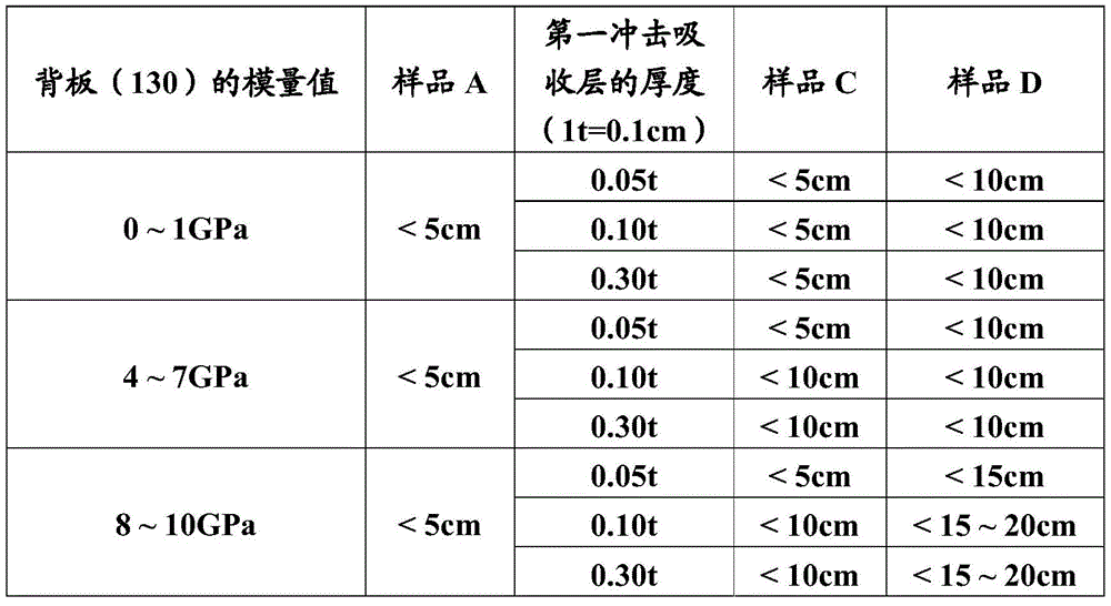
"sample A" has a modulus value of 2.2X 10⁵Pa of an optical adhesive layer and no impact-absorbing filmAnd folding the ball falling test result of the display device. The impact resistance was tested by a ball drop test using first impact absorbing layers having various thicknesses. "sample C" is the result of the falling ball test of the foldable display device having the first impact absorbing layer 171 and no second impact absorbing layer 173. In "sample C", a sample having 1.3X 10 was used3Pa modulus values of optical adhesive layers 150, 160, and 180. "sample D" is the result of the falling ball test of the foldable display device having the impact absorbing film 170 including the first impact absorbing layer 171 and the second impact absorbing layer 173. That is, in the foldable display device of "sample D", the second impact absorbing layer 173 is also included in the foldable display device of "sample C". In addition, in "sample D", the soft portion 173a had a thickness of 300 micrometers and the hard portion 173b had a thickness of 300 micrometers in the non-folded region.
As listed in Table 2, the ball drop test was substantially maintained in "sample A" and "sample C" when the modulus value of the backing plate 130 was small (e.g., 0-1 GPa). That is, although the conditions of the modulus values of the optical adhesive layers 150 and 160, the presence of the first impact absorbing layer 171, and the thickness of the first impact absorbing layer 171 are different in "sample a" and "sample C", the falling ball test is maintained. That is, the preferred backsheet 130 has a modulus value of greater than about 4 GPa.
In addition, in the case where the back sheet has a modulus value higher than 10GPa, there is a problem in the folding operation of the foldable display device. Thus, the preferred backsheet 130 may have a modulus value of about 4GPa to about 10 GPa.
In "sample C" comprising 0.05t of the first impact absorbing layer 171 and the back plate 130 having a modulus value of 4GPa to 7GPa, the ball drop test produced damage to the touch panel 120 and/or the display panel 110 at a height of 5 cm. However, in "sample C" comprising 0.10-0.30 t of the first impact absorbing layer 171 and the back plate 130 having a modulus value of 4GPa to 7GPa, the ball drop test causes damage to the touch panel 120 and/or the display panel 110 at a height of more than 10 cm. That is, preferably, the first impact absorption layer 171 may have a thickness of about 100 to 300 micrometers.
In "sample a", the ball drop test at a height of 5cm causes damage to the touch panel 120 and/or the display panel 110 regardless of the modulus value of the back plate 130.
On the other hand, the impact resistance of "sample D" was significantly improved as compared with "sample A".
That is, the impact absorbing film 170 having the first impact absorbing layer 171 and the second impact absorbing layer 173 and the impact absorbing film having the thickness of about 103In the foldable display device 100 of the first to third optical adhesive layers 150, 160, and 180 of a modulus value of Pa, external impact is released or mitigated, so that damage to the display panel 110 and/or the touch panel 120 caused by the external impact is minimized or prevented.
As described above, in the foldable display device 100 according to the second embodiment of the present invention, since high modulus elements and low modulus elements are alternately stacked in a vertical direction, external impact is released or relieved when the external impact passes through the high modulus elements and the low modulus elements. In addition, damage to the display panel 110 and/or the touch panel 120 is further reduced due to the impact absorbing film 170 under the back plate 130.
Fig. 4 is a diagram illustrating a ball drop test of a foldable display device according to the present invention.
In the graph of fig. 4, the vertical axis is the height of the sphere. "sample A" is a sample having 2.2X 10⁵Pa modulus value of the optical adhesive layer and no impact absorbing layer.
"sample D" is a foldable display device according to the second embodiment of the present invention. That is, the foldable display device in "sample D" includes the first impact absorbing layer 171 and the second impact absorbing layer 173, and each of the first to third optical adhesive layers 150, 160, and 180 has 1.3 × 10³A modulus value of Pa. The second impact absorbing layer 173, the soft portion 173a, and the hard portion 173b in the non-folded region each have a thickness of 300 micrometers.
"sample E" is a foldable display device having the second impact absorbing layer 173 without the first impact absorbing layer 171. First to third optical adhesive layers 150, 160, and 180A modulus value of 1.3 × 10³Pa and the soft 173a and hard 173b portions in the non-folded regions each have a thickness of 300 microns. That is, the foldable display device of "sample E" has the same structure except for the first impact absorbing layer.
The folding region "FR" is a folding region having a curvature in a folding operation, and the non-folding region "NFR" is a region having a substantially flat state in a folding operation. The non-folding region "NFR" is located on both sides of the folding region "FR". The bar graph is the minimum height of the ball that creates the lesion on the foldable display device.
As shown in fig. 4, in the folding region "FR", there was a damage on the foldable display device at a ball height of 5cm (sample a), and a damage on the foldable display device at a ball height of 15 cm (sample D).
In the non-folded region "NFR", there was a damage on the foldable display device at a ball height of 20 cm (sample a) and at a ball height of 30 cm (sample D).
That is, since high modulus elements and low modulus elements are alternately stacked in a vertical direction and an impact absorbing film including a first impact absorbing layer and a second impact absorbing layer is formed at a rear side of a back plate in the foldable display device of the present invention, the foldable display device of the present invention has improved impact resistance performance compared to the foldable display device of the related art. Accordingly, damage to the foldable display device 100 caused by impact is minimized or prevented.
In addition, as shown in the ball drop test in "sample D" and "sample E", damage is easily generated on the foldable display device without the first impact absorbing layer.
That is, as shown in the ball drop test in "sample C" and "sample D" of table 2, the foldable display device including the first impact absorbing layer and the second impact absorbing layer has reduced damage as compared to the foldable display device including the first impact absorbing layer without the second impact absorbing layer. In addition, as shown in the ball drop test in "sample D" and "sample E" of fig. 4, the foldable display device including the first impact absorbing layer and the second impact absorbing layer has less damage as compared to the foldable display device including the second impact absorbing layer without the first impact absorbing layer.
In addition, when the back plate 130 has a relatively low modulus value, damage through the back plate 130 is prevented by the shock-absorbing film 170, so that the production cost of the back plate 130 is reduced.
TABLE 3

The results of the ball drop test on the foldable display device with respect to the modulus values of the optical adhesive layer and the presence of the impact absorbing film are listed in table 3.
"sample F" is a result of a ball drop test on a foldable display device without an impact absorbing film, and "sample D" is a result of a ball drop test on a foldable display device with an impact absorbing film 170 including a first impact absorbing layer 171 and a second impact absorbing layer 173. In "sample D", the thickness of the first impact absorption layer was 200 micrometers, and the thickness of each of the soft portion 173a and the hard portion 173b in the non-folded region was 300 micrometers. That is, the total thickness of the second impact absorbing layer was 600 μm.
In the foldable display device, each of the cover window 140, the touch panel 120, and the display panel 110 has a modulus value of 5GPa to 8GPa, and the back sheet 130 has a modulus value of 8GPa to 10 GPa.
As listed in Table 3, each of the first optical adhesive layer 150 between the cover window 140 and the touch panel 120 and the second optical adhesive layer 160 between the display panel 110 and the back plate 130 has a relatively low modulus value, i.e., 1.3 × 10³Pa, improved impact resistance in both foldable display devices without the impact absorbing film ("sample F") and with the impact absorbing film ("sample D").
In more detail, in "sample F", the optical adhesive layer had a high modulus value, i.e., about 2.2X 10⁵In the case of (1), damage to the touch panel 120 and/or the display panel 110 is generated in a ball drop test at a height of 5cm, while damage is generated in an optical testThe adhesive layer has a low modulus value, i.e. about 1.3X 10³In the case of (2), damage to the touch panel 120 and/or the display panel 110 is generated in a ball drop test at a height of 10 cm.
That is, damage on the display panel 110 and/or the touch panel 120 depends on the modulus values of the optical adhesive layers 150 and 160. And have each of them have a relatively high modulus value, e.g., 2.2 x 10⁵Compared to a foldable display device having optical adhesive layers 150 and 160, having a relatively low modulus value, e.g., 1.3 x 10, for each3The foldable display device of optical adhesive layers 150 and 160 in which damage on the display panel 110 and/or the touch panel 120 is minimized.
In addition, in "sample D" having a low modulus optical adhesive layer and the impact absorbing film 170 including the first impact absorbing layer 171 and the second impact absorbing layer 173, the impact resistance of the foldable display device was further improved.
That is, in the foldable display device 100 according to the second embodiment of the present invention, since the high modulus elements and the low modulus elements are alternately stacked in the vertical direction, external impact is released or mitigated when the external impact passes through the high modulus elements and the low modulus elements. In addition, damage to the display panel 110 and/or the touch panel 120 is further reduced due to the impact absorbing film 170 under the back plate 130.
In fig. 1 and 3, the foldable display device 100 includes a touch panel 120 at one side of the display panel 110. However, the touch panel 120 may be omitted. In this case, the first optical adhesive layer 150 contacts the display panel 110 without the touch panel 120.
It will be apparent to those skilled in the art that various modifications and variations can be made in the present invention without departing from the scope of the invention.
The following is a list of preferred embodiments:
a foldable display device comprising: a display panel; a cover window at a first side of the display panel; a shock absorbing film including a first shock absorbing layer and a second shock absorbing layer at a second side of the display panel; and a back plate between the display panel and the impact absorbing film and including a folding region and a non-folding region, wherein the second impact absorbing layer includes a soft portion corresponding to the folding region and a hard portion corresponding to the non-folding region, and each of the first impact absorbing layer and the soft portion has a modulus value smaller than that of the hard portion.
The first impact absorption layer preferably includes a foam type material, and the soft part includes one of Polyurethane (PU), Thermoplastic Polyurethane (TPU), silicon (Si), and Polydimethylacrylamide (PDMA), and wherein the hard part includes one of stainless steel (SUS), PMMA, Polycarbonate (PC), polyvinyl alcohol (PVA), acrylonitrile-butadiene-styrene (ABS), and polyethylene terephthalate (PET).
The first impact absorbing layer preferably has a thickness of about 100 to 300 microns. The second impact absorbing layer preferably has a thickness of about 0.1mm to 1 mm. The soft portion preferably has a thickness of about 0 to 0.9mm in the non-folded region. The hard portion preferably has a thickness of about 0.1mm to 1 mm.
The modulus value of the first impact-absorbing layer preferably has a value of about 103Pa to 104Pa range. The modulus value of the soft segment preferably has a value of about 103Pa to 104Pa, and the modulus value of the hard portion has a range of about 5GPa to 8 GPa.
The display device preferably further comprises a first optical adhesive layer between the cover window and the display panel and having a modulus value smaller than the cover window and the display panel; and a second optical adhesive layer between the display panel and the backplane and having a modulus value less than the display panel and the backplane. The modulus value of each of the first and second optical adhesive layers preferably has a value of about 103Pa to 104Pa range.
The display device preferably further comprises a third optical adhesive layer between the impact absorbing film and the back plate and having a modulus value smaller than that of the back plate. The modulus value of the third optical adhesive layer preferably has a value of about 103Pa to 104Pa range.
The display device preferably further includes a touch panel between the display panel and the cover window; to be provided withAnd an optical adhesive layer between the touch panel and the cover window. The modulus value of the optical adhesive layer is preferably less than the touch panel and the cover window. The modulus value of the optical adhesive layer preferably has about 103Pa to 104Pa range.
The first and second impact absorbing layers are preferably attached to each other by an optical adhesive layer.
The non-folded region preferably includes a first non-folded region and a second non-folded region on either side of the folded region. The rigid portion preferably comprises a first portion and a second portion in the first unfolded region and the second unfolded region, respectively. The portion of the soft portion corresponding to the fold area is preferably inserted into the space between the first and second portions of the hard portion.
The display panel preferably includes a plurality of pixel regions. The boundaries of the folding area and the non-folding area preferably correspond to the boundaries of adjacent pixel areas.
According to another preferred embodiment, a foldable display panel includes: a display panel; a cover window at one side of the display panel; a first optical adhesive layer between the display panel and the cover window; a back plate at a second side of the display panel; and a second optical adhesive layer between the display panel and the backplane, wherein a modulus value of the first optical adhesive layer is less than the display panel and the cover window, and a modulus value of the second optical adhesive layer is less than the display panel and the cover window.
The foldable display device preferably further comprises an impact absorbing layer under the back plate; and a third optical adhesive layer between the impact absorbing layer and the backsheet, wherein the impact absorbing layer has a modulus value less than the backsheet.
Claims (17)
1. A foldable display device comprising:
a display panel including a first surface and a second surface opposite to the first surface;
a shock absorbing film including a first shock absorbing layer and a second shock absorbing layer disposed at the second surface of the display panel; and
a back plate disposed between the display panel and the impact absorption film;
wherein the second impact absorbing layer includes a soft portion corresponding to a first region of the second impact absorbing layer and a hard portion corresponding to a second region of the second impact absorbing layer, an
The elastic modulus values of the soft portion and the first impact absorbing layer of the second impact absorbing layer are smaller than the elastic modulus value of the hard portion;
the soft portion is formed of a single material.
2. The foldable display device of claim 1, wherein the first region is interposed between two portions of the second region, and wherein the first region corresponds to a folded region and the second region corresponds to a non-folded region.
3. The foldable display device of claim 1, wherein the first impact absorbing layer comprises a foam-type material.
4. The foldable display device of claim 1, wherein the first impact absorbing layer is disposed between the second impact absorbing layer and the display panel.
5. The foldable display device of claim 1, wherein the thickness of the first impact absorbing layer is in a range of 100 to 300 microns.
6. The foldable display device of claim 1, wherein at least one of the first impact absorbing layer and the soft portion has an elastic modulus of 103Pa to 104Pa, in the range of Pa.
7. The foldable display device of claim 1, wherein the thickness of the hard portion of the second impact absorbing layer is in a range of 100 to 1000 microns.
8. The foldable display device of claim 1, wherein the thickness of the hard portion of the second impact absorbing layer is in a range of 100 to 500 micrometers.
9. The foldable display device of claim 1, wherein the soft portion and the hard portion of the second impact absorbing layer form a double-layer structure.
10. The foldable display device of claim 9, wherein the soft portion comprises a base portion extending over both the first area and the second area, and a protruding portion corresponding to the first area and protruding from the base portion, the protruding portion being interposed between two portions of the hard portion.
11. The foldable display device of claim 1, wherein an interface between the first region and the second region is aligned with a boundary between adjacent pixel regions of the display panel.
12. The foldable display device of claim 1, further comprising:
a cover window disposed at the first surface of the display panel; and
a first optical adhesive layer for attaching the cover window to the display panel; and
a second optical adhesive layer for attaching the backplane to the display panel,
wherein the first optical adhesive layer has a modulus of elasticity less than the modulus of elasticity of the display panel and the cover window, and the second optical adhesive layer has a modulus of elasticity less than the modulus of elasticity of the display panel and the backplane.
13. The foldable display device of claim 12, further comprising:
a third optical adhesive layer for attaching the shock absorbing film to the backplane,
wherein the third optical adhesive layer has a modulus of elasticity less than the modulus of elasticity of the display panel and the backplane.
14. The foldable display device of claim 13, wherein at least one of the first to third optical adhesive layers has a thickness in a range of 100 to 300 microns.
15. The foldable display device of claim 13, wherein at least one of the first to third optical adhesive layers has an elastic modulus of 103Pa to 104Pa, in the range of Pa.
16. The foldable display device of claim 1, further comprising: a touch panel disposed on the first surface of the display panel.
17. The foldable display device of claim 12, wherein a modulus value of each of the soft portion of the second impact absorbing layer and the first impact absorbing layer is less than a modulus value of the cover window, the display panel, and the back plate.
Applications Claiming Priority (6)
| Application Number | Priority Date | Filing Date | Title |
|---|---|---|---|
| KR10-2015-0169503 | 2015-11-30 | ||
| KR20150169503 | 2015-11-30 | ||
| KR1020160048801A KR20170064453A (en) | 2015-11-30 | 2016-04-21 | Foldable display device |
| KR10-2016-0048801 | 2016-04-21 | ||
| KR1020160120655A KR102588088B1 (en) | 2015-11-30 | 2016-09-21 | Foldable display device |
| KR10-2016-0120655 | 2016-09-21 |
Publications (2)
| Publication Number | Publication Date |
|---|---|
| CN106875845A CN106875845A (en) | 2017-06-20 |
| CN106875845B true CN106875845B (en) | 2020-01-10 |
Family
ID=59219995
Family Applications (1)
| Application Number | Title | Priority Date | Filing Date |
|---|---|---|---|
| CN201611044740.0A Active CN106875845B (en) | 2015-11-30 | 2016-11-24 | Foldable display device |
Country Status (2)
| Country | Link |
|---|---|
| KR (2) | KR20170064453A (en) |
| CN (1) | CN106875845B (en) |
Families Citing this family (40)
| Publication number | Priority date | Publication date | Assignee | Title |
|---|---|---|---|---|
| US11262482B2 (en) | 2017-08-14 | 2022-03-01 | Industrial Technology Research Institute | Impact resistant structure and electronic device |
| CN109390288B (en) * | 2017-08-14 | 2022-01-28 | 财团法人工业技术研究院 | Impact-resistant shock-absorbing structure and electronic device |
| KR102436547B1 (en) * | 2017-09-29 | 2022-08-29 | 삼성디스플레이 주식회사 | Electronic device |
| KR102012444B1 (en) | 2017-10-31 | 2019-08-20 | 엘지디스플레이 주식회사 | Foldable display device and its manufacturing method |
| KR102454623B1 (en) * | 2017-12-29 | 2022-10-13 | 엘지디스플레이 주식회사 | Foldable display device and method of manufacturing the same |
| KR102547124B1 (en) * | 2018-03-30 | 2023-06-26 | 삼성디스플레이 주식회사 | Display device |
| TWI661344B (en) * | 2018-04-13 | 2019-06-01 | 友達光電股份有限公司 | Display device |
| KR102452238B1 (en) | 2018-05-11 | 2022-10-07 | 삼성디스플레이 주식회사 | Display device |
| KR102579330B1 (en) | 2018-05-18 | 2023-09-18 | 삼성디스플레이 주식회사 | Display apparatus and method of manufacturing the same |
| KR102549716B1 (en) | 2018-07-16 | 2023-07-03 | 삼성디스플레이 주식회사 | Display apparatus |
| CN109036133A (en) * | 2018-07-28 | 2018-12-18 | 蒙凤英 | Backboard and display component |
| KR102545647B1 (en) * | 2018-08-13 | 2023-06-19 | 엘지디스플레이 주식회사 | Foldable display device |
| KR102533507B1 (en) * | 2018-08-13 | 2023-05-16 | 엘지디스플레이 주식회사 | Foldable display device |
| KR102482409B1 (en) | 2018-08-21 | 2022-12-28 | 삼성디스플레이 주식회사 | Display device |
| JP7083030B2 (en) * | 2018-08-28 | 2022-06-09 | 富士フイルム株式会社 | Liquid crystal panel and image display device |
| KR102519732B1 (en) * | 2018-09-19 | 2023-04-11 | 삼성전자주식회사 | Foldable electronic device including integral type adhesive layer and adhesion prevention part |
| KR102586636B1 (en) | 2018-10-11 | 2023-10-11 | 삼성디스플레이 주식회사 | Foldable display device |
| KR20200042579A (en) | 2018-10-15 | 2020-04-24 | 삼성디스플레이 주식회사 | Display device |
| KR102484586B1 (en) * | 2018-11-07 | 2023-01-03 | 엘지디스플레이 주식회사 | Foldable display device |
| KR102524510B1 (en) * | 2018-11-21 | 2023-04-20 | 엘지디스플레이 주식회사 | Foldable display device |
| KR102262695B1 (en) | 2018-11-22 | 2021-06-08 | 주식회사 엘지화학 | Foldable backplate, manufacturing method of foldable backplate and foldable display device comprising the same |
| KR102639989B1 (en) * | 2018-12-28 | 2024-02-22 | 엘지디스플레이 주식회사 | Flexible display device |
| US10795415B2 (en) * | 2019-01-30 | 2020-10-06 | Motorola Mobility Llc | Foldable display with stiff support |
| KR102654292B1 (en) | 2019-02-01 | 2024-04-03 | 삼성디스플레이 주식회사 | Flexible display device |
| KR20200098801A (en) | 2019-02-12 | 2020-08-21 | 삼성디스플레이 주식회사 | Electronic apparatus |
| KR102632543B1 (en) * | 2019-02-19 | 2024-02-01 | 삼성디스플레이 주식회사 | Display device including bonding member |
| KR20200101220A (en) * | 2019-02-19 | 2020-08-27 | 삼성전자주식회사 | Foldable electronic device comprising multiple windows |
| KR20200103240A (en) * | 2019-02-22 | 2020-09-02 | 삼성디스플레이 주식회사 | Display device |
| KR20200104446A (en) | 2019-02-26 | 2020-09-04 | 삼성디스플레이 주식회사 | Display apparatus |
| KR20210000809A (en) * | 2019-06-25 | 2021-01-06 | 삼성디스플레이 주식회사 | Display device |
| US11956906B2 (en) | 2019-07-30 | 2024-04-09 | Boe Technology Group Co., Ltd. | Backboard support structure, preparation method therefor, and the display device |
| CN110570760B (en) * | 2019-08-13 | 2022-01-04 | 武汉华星光电半导体显示技术有限公司 | Foldable flexible display device |
| KR20210073253A (en) | 2019-12-10 | 2021-06-18 | 엘지디스플레이 주식회사 | Foldable display device |
| KR20210085033A (en) | 2019-12-30 | 2021-07-08 | 엘지디스플레이 주식회사 | Foldable display device |
| CN111292621B (en) * | 2020-02-24 | 2021-12-24 | 京东方科技集团股份有限公司 | Display device, support film for display device, and electronic apparatus |
| JP2021148834A (en) * | 2020-03-16 | 2021-09-27 | 株式会社Joled | Display device and electronic apparatus |
| KR20220006670A (en) | 2020-07-08 | 2022-01-18 | 삼성디스플레이 주식회사 | Display device |
| US11327531B2 (en) * | 2020-09-30 | 2022-05-10 | Sharp Kabushiki Kaisha | Foldable display panel with shock absorber |
| CN112365802B (en) | 2020-11-24 | 2022-05-17 | 湖北长江新型显示产业创新中心有限公司 | Display device and manufacturing method thereof |
| KR20230000264A (en) * | 2021-06-24 | 2023-01-02 | 삼성전자주식회사 | Electronic device including foldable display |
Citations (2)
| Publication number | Priority date | Publication date | Assignee | Title |
|---|---|---|---|---|
| CN104424851A (en) * | 2013-08-19 | 2015-03-18 | 三星显示有限公司 | Foldable display device |
| CN104900149A (en) * | 2014-03-05 | 2015-09-09 | 乐金显示有限公司 | Foldable display apparatus |
Family Cites Families (4)
| Publication number | Priority date | Publication date | Assignee | Title |
|---|---|---|---|---|
| KR100929706B1 (en) * | 2007-10-12 | 2009-12-03 | 주식회사 근수산업 | Adhesive Pad |
| WO2009103857A1 (en) * | 2008-02-21 | 2009-08-27 | Marisense Oy | Display module and related manufacturing method |
| KR102132235B1 (en) * | 2013-11-28 | 2020-07-10 | 삼성디스플레이 주식회사 | Flexible display device |
| KR102133213B1 (en) * | 2013-12-18 | 2020-07-15 | 삼성디스플레이 주식회사 | Substrate for display device, method of manufacturing the same, and display device including the same |
-
2016
- 2016-04-21 KR KR1020160048801A patent/KR20170064453A/en unknown
- 2016-09-21 KR KR1020160120655A patent/KR102588088B1/en active IP Right Grant
- 2016-11-24 CN CN201611044740.0A patent/CN106875845B/en active Active
Patent Citations (2)
| Publication number | Priority date | Publication date | Assignee | Title |
|---|---|---|---|---|
| CN104424851A (en) * | 2013-08-19 | 2015-03-18 | 三星显示有限公司 | Foldable display device |
| CN104900149A (en) * | 2014-03-05 | 2015-09-09 | 乐金显示有限公司 | Foldable display apparatus |
Also Published As
| Publication number | Publication date |
|---|---|
| KR20170064453A (en) | 2017-06-09 |
| KR20170063344A (en) | 2017-06-08 |
| KR102588088B1 (en) | 2023-10-12 |
| CN106875845A (en) | 2017-06-20 |
Similar Documents
| Publication | Publication Date | Title |
|---|---|---|
| CN106875845B (en) | Foldable display device | |
| US10198038B2 (en) | Foldable display device | |
| CN107768539B (en) | Flexible display device | |
| KR102633501B1 (en) | Foldable display device | |
| US11500423B2 (en) | Flexible display device | |
| CN110858461B (en) | Flexible display device | |
| KR20170070309A (en) | Backplate and foldable display device including the same | |
| US20180034001A1 (en) | Window for a display device and a flexible display device including the same | |
| EP3493038B1 (en) | Touch panel and display device including the same | |
| KR20170072973A (en) | Optical cleared adhesive and foldable display device including the same | |
| US10826025B2 (en) | Flexible display device | |
| US20240065022A1 (en) | Foldable display device | |
| US11776436B2 (en) | Foldable display device | |
| KR20170064161A (en) | Optical cleared adhesive and foldable display device including the same | |
| US20230006179A1 (en) | Flexible display device | |
| KR20220022926A (en) | Display device | |
| KR20170064160A (en) | Foldable display device | |
| KR20200052167A (en) | Foldable display device | |
| US20220399511A1 (en) | Display device and electronic apparatus including the same | |
| CN117642019A (en) | Display device | |
| KR20200066919A (en) | Organic light emitting display device |
Legal Events
| Date | Code | Title | Description |
|---|---|---|---|
| PB01 | Publication | ||
| PB01 | Publication | ||
| SE01 | Entry into force of request for substantive examination | ||
| SE01 | Entry into force of request for substantive examination | ||
| GR01 | Patent grant | ||
| GR01 | Patent grant |