CN106716839B - Analog cancellation of ungrounded conductive objects in capacitive sensing - Google Patents
Analog cancellation of ungrounded conductive objects in capacitive sensing Download PDFInfo
- Publication number
- CN106716839B CN106716839B CN201580052185.3A CN201580052185A CN106716839B CN 106716839 B CN106716839 B CN 106716839B CN 201580052185 A CN201580052185 A CN 201580052185A CN 106716839 B CN106716839 B CN 106716839B
- Authority
- CN
- China
- Prior art keywords
- measurement
- capacitance
- self
- capacitor
- capacitive sensor
- Prior art date
- Legal status (The legal status is an assumption and is not a legal conclusion. Google has not performed a legal analysis and makes no representation as to the accuracy of the status listed.)
- Active
Links
Images


Classifications
-
- G—PHYSICS
- G06—COMPUTING; CALCULATING OR COUNTING
- G06F—ELECTRIC DIGITAL DATA PROCESSING
- G06F3/00—Input arrangements for transferring data to be processed into a form capable of being handled by the computer; Output arrangements for transferring data from processing unit to output unit, e.g. interface arrangements
- G06F3/01—Input arrangements or combined input and output arrangements for interaction between user and computer
- G06F3/03—Arrangements for converting the position or the displacement of a member into a coded form
- G06F3/041—Digitisers, e.g. for touch screens or touch pads, characterised by the transducing means
- G06F3/0416—Control or interface arrangements specially adapted for digitisers
- G06F3/0418—Control or interface arrangements specially adapted for digitisers for error correction or compensation, e.g. based on parallax, calibration or alignment
- G06F3/04186—Touch location disambiguation
-
- G—PHYSICS
- G06—COMPUTING; CALCULATING OR COUNTING
- G06F—ELECTRIC DIGITAL DATA PROCESSING
- G06F3/00—Input arrangements for transferring data to be processed into a form capable of being handled by the computer; Output arrangements for transferring data from processing unit to output unit, e.g. interface arrangements
- G06F3/01—Input arrangements or combined input and output arrangements for interaction between user and computer
- G06F3/03—Arrangements for converting the position or the displacement of a member into a coded form
- G06F3/041—Digitisers, e.g. for touch screens or touch pads, characterised by the transducing means
- G06F3/044—Digitisers, e.g. for touch screens or touch pads, characterised by the transducing means by capacitive means
-
- H—ELECTRICITY
- H03—ELECTRONIC CIRCUITRY
- H03K—PULSE TECHNIQUE
- H03K17/00—Electronic switching or gating, i.e. not by contact-making and –breaking
- H03K17/94—Electronic switching or gating, i.e. not by contact-making and –breaking characterised by the way in which the control signals are generated
- H03K17/96—Touch switches
- H03K17/962—Capacitive touch switches
-
- G—PHYSICS
- G06—COMPUTING; CALCULATING OR COUNTING
- G06F—ELECTRIC DIGITAL DATA PROCESSING
- G06F2203/00—Indexing scheme relating to G06F3/00 - G06F3/048
- G06F2203/041—Indexing scheme relating to G06F3/041 - G06F3/045
- G06F2203/04107—Shielding in digitiser, i.e. guard or shielding arrangements, mostly for capacitive touchscreens, e.g. driven shields, driven grounds
-
- H—ELECTRICITY
- H03—ELECTRONIC CIRCUITRY
- H03K—PULSE TECHNIQUE
- H03K17/00—Electronic switching or gating, i.e. not by contact-making and –breaking
- H03K17/94—Electronic switching or gating, i.e. not by contact-making and –breaking characterised by the way in which the control signals are generated
- H03K17/96—Touch switches
- H03K2017/9602—Touch switches characterised by the type or shape of the sensing electrodes
- H03K2017/9604—Touch switches characterised by the type or shape of the sensing electrodes characterised by the number of electrodes
- H03K2017/9606—Touch switches characterised by the type or shape of the sensing electrodes characterised by the number of electrodes using one electrode only per touch switch
-
- H—ELECTRICITY
- H03—ELECTRONIC CIRCUITRY
- H03K—PULSE TECHNIQUE
- H03K17/00—Electronic switching or gating, i.e. not by contact-making and –breaking
- H03K17/94—Electronic switching or gating, i.e. not by contact-making and –breaking characterised by the way in which the control signals are generated
- H03K17/96—Touch switches
- H03K2017/9602—Touch switches characterised by the type or shape of the sensing electrodes
- H03K2017/9604—Touch switches characterised by the type or shape of the sensing electrodes characterised by the number of electrodes
- H03K2017/9613—Touch switches characterised by the type or shape of the sensing electrodes characterised by the number of electrodes using two electrodes per touch switch
-
- H—ELECTRICITY
- H03—ELECTRONIC CIRCUITRY
- H03K—PULSE TECHNIQUE
- H03K2217/00—Indexing scheme related to electronic switching or gating, i.e. not by contact-making or -breaking covered by H03K17/00
- H03K2217/94—Indexing scheme related to electronic switching or gating, i.e. not by contact-making or -breaking covered by H03K17/00 characterised by the way in which the control signal is generated
- H03K2217/9401—Calibration techniques
- H03K2217/94026—Automatic threshold calibration; e.g. threshold automatically adapts to ambient conditions or follows variation of input
-
- H—ELECTRICITY
- H03—ELECTRONIC CIRCUITRY
- H03K—PULSE TECHNIQUE
- H03K2217/00—Indexing scheme related to electronic switching or gating, i.e. not by contact-making or -breaking covered by H03K17/00
- H03K2217/94—Indexing scheme related to electronic switching or gating, i.e. not by contact-making or -breaking covered by H03K17/00 characterised by the way in which the control signal is generated
- H03K2217/9401—Calibration techniques
- H03K2217/94031—Calibration involving digital processing
-
- H—ELECTRICITY
- H03—ELECTRONIC CIRCUITRY
- H03K—PULSE TECHNIQUE
- H03K2217/00—Indexing scheme related to electronic switching or gating, i.e. not by contact-making or -breaking covered by H03K17/00
- H03K2217/94—Indexing scheme related to electronic switching or gating, i.e. not by contact-making or -breaking covered by H03K17/00 characterised by the way in which the control signal is generated
- H03K2217/96—Touch switches
- H03K2217/9607—Capacitive touch switches
- H03K2217/960705—Safety of capacitive touch and proximity switches, e.g. increasing reliability, fail-safe
-
- H—ELECTRICITY
- H03—ELECTRONIC CIRCUITRY
- H03K—PULSE TECHNIQUE
- H03K2217/00—Indexing scheme related to electronic switching or gating, i.e. not by contact-making or -breaking covered by H03K17/00
- H03K2217/94—Indexing scheme related to electronic switching or gating, i.e. not by contact-making or -breaking covered by H03K17/00 characterised by the way in which the control signal is generated
- H03K2217/96—Touch switches
- H03K2217/9607—Capacitive touch switches
- H03K2217/96071—Capacitive touch switches characterised by the detection principle
- H03K2217/960725—Charge-transfer
-
- H—ELECTRICITY
- H03—ELECTRONIC CIRCUITRY
- H03K—PULSE TECHNIQUE
- H03K2217/00—Indexing scheme related to electronic switching or gating, i.e. not by contact-making or -breaking covered by H03K17/00
- H03K2217/94—Indexing scheme related to electronic switching or gating, i.e. not by contact-making or -breaking covered by H03K17/00 characterised by the way in which the control signal is generated
- H03K2217/96—Touch switches
- H03K2217/9607—Capacitive touch switches
- H03K2217/960755—Constructional details of capacitive touch and proximity switches
- H03K2217/960765—Details of shielding arrangements
-
- H—ELECTRICITY
- H03—ELECTRONIC CIRCUITRY
- H03K—PULSE TECHNIQUE
- H03K2217/00—Indexing scheme related to electronic switching or gating, i.e. not by contact-making or -breaking covered by H03K17/00
- H03K2217/94—Indexing scheme related to electronic switching or gating, i.e. not by contact-making or -breaking covered by H03K17/00 characterised by the way in which the control signal is generated
- H03K2217/96—Touch switches
- H03K2217/9607—Capacitive touch switches
- H03K2217/960755—Constructional details of capacitive touch and proximity switches
- H03K2217/960775—Emitter-receiver or "fringe" type detection, i.e. one or more field emitting electrodes and corresponding one or more receiving electrodes
Abstract
The invention relates to a method for performing touch determination with a capacitive sensor by initiating a self-capacitance measurement of the capacitive sensor (150), wherein a mutual capacitance measurement comprising the capacitive sensor is performed simultaneously. This method may be performed such that the self-capacitance measurement and the mutual capacitance measurement cancel differentially as an ungrounded conductive object approaches or touches the capacitive sensor and additively combine for a grounded object approaching or touching the capacitive sensor.
Description
CROSS-REFERENCE TO RELATED APPLICATIONS
This application claims the benefit of united states provisional patent application No. 62/068,450, filed on day 24, 10/2014, which is incorporated herein by reference in its entirety.
Technical Field
The present invention relates to capacitance sensing, and in particular, to analog cancellation of ungrounded conductive objects (e.g., high permittivity objects) in capacitance sensing.
Background
Capacitive touch surfaces need to avoid contamination to function properly. However, capacitive touch sensing in particular embodiments exposes the touch surface to liquids or other materials that contaminate the surface and have a detrimental effect on the sensing characteristics. Thus, there is a need for capacitive touch sensing that is not affected by contamination of the touch surface, particularly water on the touch surface.
Existing solutions for water resistance in capacitive sensing use only mutual capacitance and cause a negative shift on the signal when water is introduced into the system and a positive shift when a finger is introduced. When water is removed from the system, false triggers can occur if removing a negative shift makes a positive shift too large.
Other solutions to this problem use software pattern matching algorithms to detect differences in behavior between water and fingers. This results in a large amount of overhead and does not take into account all behavioral patterns.
Disclosure of Invention
According to an embodiment, in a method for performing touch determination with a capacitive sensor, a self-capacitance measurement of the capacitive sensor is initiated, wherein a mutual capacitance measurement comprising the capacitive sensor is performed simultaneously.
According to a further embodiment, after the sensor has been set to a high impedance state during the self-capacitance measurement, a pulse may be capacitively coupled into the capacitive sensor for performing the mutual capacitance measurement. According to a further embodiment, a shield or guard electrode may be arranged close to the capacitive sensor to provide capacitive coupling. According to a further embodiment, the self-capacitance measurement may be a capacitive voltage divider measurement. According to a further embodiment, the self-capacitance measurement is a charge time measurement. According to a further embodiment, the method may further comprise a calibration method, wherein the calibration method is performed before the touch determination is performed. The calibration method may comprise the steps of: performing individual self-capacitance measurements and storing a first measurement value; performing individual mutual capacitance measurements and storing a second measurement value; and calculating a scaling factor from said first and said second measurements; wherein the method for performing touch determination includes applying the scaling factor to the self capacitance or the mutual capacitance measurement.
According to another embodiment, a method for performing touch determination with a capacitive sensor may comprise the steps of: charging a first capacitor to a first level and a second capacitor of the sensor to a second level; coupling first and second capacitors in parallel while the sensor is set to a high impedance and feeding a pulse to a protection sensor capacitively coupled with the sensor; determining a first settled voltage level of the parallel coupled capacitors after a settling phase; thereafter, charging the first capacitor to the second level and charging the second capacitor of the sensor to the first level; coupling first and second capacitors in parallel while setting the sensor to a high impedance, wherein the pulse is terminated upon coupling of the first and second capacitors; and determining a second settled voltage level of the parallel coupled capacitors after settling the phase.
According to a further embodiment, the first level may be a predetermined voltage VDDAnd the second voltage level is a ground level VSS. According to a further embodiment, the second level may be a predetermined voltage VDDAnd the first voltage level is a ground level VSS. According to a further embodiment, the pulse may have a voltage level VDDAnd begins after expiration of a predetermined period of time that begins when the first and second capacitors are coupled in parallel.
According to a further embodiment, a microcontroller for performing touch determination with a capacitive sensor may comprise: a capacitance measurement unit configurable to perform self-capacitance measurements and mutual capacitance measurements, and comprising a control unit operable to: initiating a self-capacitance measurement of a capacitance sensor coupled with the capacitance measurement unit, wherein a mutual capacitance measurement including the capacitance sensor is performed simultaneously.
According to a further embodiment of the microcontroller, the capacitance measurement unit may be configured to switch to a high impedance state during the self-capacitance measurement and capacitively couple a pulse into the capacitance sensor for the mutual capacitance measurement. According to a further embodiment of the microcontroller, the capacitance measuring unit comprises a capacitive voltage divider measuring unit. According to a further embodiment of the microcontroller, the capacitive voltage divider measurement unit may comprise: a first switching unit coupled between an external pin and a sample and hold capacitor and operable to charge an externally connected capacitor to a first or second voltage level or switch the externally connected capacitor in parallel with the sample and hold capacitor; a second switching unit coupled with the sample and hold capacitor and operable to charge the sample and hold capacitor to the first or the second voltage level; an analog-to-digital converter operable to couple with the parallel-switched capacitor; and wherein the control unit is configured to control the first and the second switching units. According to a further embodiment of the microcontroller, the microcontroller may further comprise a second external pin coupled with an input/output port, the input/output port being configurable to operate as an output port, wherein the control unit is configured to control the output port for performing mutual capacitance measurements. According to a further embodiment of the microcontroller, the capacitance measuring unit may comprise a charge time measurement, wherein the control unit is configured to control the self-capacitance measurement with the charge time measuring unit, wherein the charge time measuring unit is connected with a first external pin, which may be connected with a capacitance sensor. According to a further embodiment of the microcontroller, the microcontroller may further comprise a second external pin coupled with an input/output port, the input/output port being configurable to operate as an output port, wherein the control unit is configured to control the output port for performing mutual capacitance measurements. According to a further embodiment of the microcontroller, the control unit may be configured to perform a calibration before performing a touch determination, the control unit controlling: individual self-capacitance measurements and storing a first measurement value; individual mutual capacitance measurements and storing a second measurement value; and wherein the control unit or processor of the microcontroller is configured to calculate a scaling factor from the first and the second measurements; wherein to perform a touch determination, the control unit is configured to apply the scaling factor to the self capacitance or the mutual capacitance measurement. According to a further embodiment of the microcontroller, the scaling factor may change a charge level during the self-capacitance measurement or a voltage level during the mutual capacitance measurement.
According to a further embodiment, a system may comprise such a microcontroller, and further comprise the capacitive sensor connected with the microcontroller through the first external pin and a shielding or guard electrode arranged close to the capacitive sensor connected with the second external pin.
According to yet another embodiment, a method for performing touch determination with a capacitive sensor may comprise the steps of: initiating a self-capacitance measurement of a capacitive sensor, initiating a mutual capacitance measurement comprising the capacitive sensor; performing a scaling of either the output value of the self-capacitance measurement or the mutual capacitance measurement; and combining the output values of the self-capacitance measurement and the mutual-capacitance measurement.
According to a further embodiment of the above method, the method may further comprise combining the output values (comprising adding the output values). According to a further embodiment of the above method, a shielding or guard electrode may be arranged close to the capacitive sensor to provide capacitive coupling. According to a further embodiment of the above method, the self-capacitance measurement may be a capacitive voltage divider measurement. According to a further embodiment of the above method, the self-capacitance measurement may be a charge time measurement. According to a further embodiment of the above method, the method may further comprise a calibration method to determine the scale factor, wherein the calibration method is performed before performing the touch determination, the calibration method comprising: performing individual self-capacitance measurements and storing a first measurement value; performing individual mutual capacitance measurements and storing a second measurement value; and calculating a scaling factor from the first and second measurements.
According to a further embodiment, a method for performing touch determination with a capacitive sensor may comprise the steps of initiating a self-capacitance measurement of a capacitive sensor, wherein a mutual capacitance measurement including the capacitive sensor is performed simultaneously such that the self-capacitance measurement and the mutual capacitance measurement cancel differentially as ungrounded conductive objects approach or touch the capacitive sensor and combine additively for grounded objects approaching or touching the capacitive sensor.
Drawings
FIGS. 1 and 2 show a conventional arrangement with a capacitive touch sensor for measuring self-capacitance;
FIG. 3 shows a related timing diagram of self-capacitance measurement;
FIGS. 4 and 5 show the effects of sensor contamination and user touch, respectively;
FIG. 6 shows an arrangement of capacitive touch sensors according to various embodiments;
FIGS. 7a, b, c show an embodiment of a guard or shield electrode;
fig. 8 explains the measuring principle using the arrangement according to fig. 6;
FIG. 9 shows a related timing diagram;
FIGS. 10-13 show the effects of sensor contamination and user touch, respectively;
FIGS. 14 and 15 show timing diagrams of respective first and second measurements of self-capacitance, mutual capacitance, and combinations thereof with and without contamination;
FIG. 16 shows a timing diagram of processed output values for a user touch event with a dirty and non-dirty sensor;
FIG. 17 shows an example of an arrangement using different capacitance measurement systems according to other embodiments; and
fig. 18 shows the effect of scaling measurements.
Detailed Description
According to various embodiments, self-capacitance and mutual capacitance are combined to eliminate analog signal shifts of high permittivity objects, such as ungrounded conductive objects (e.g., water, detergents, and gasoline).
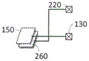
Self-capacitance and mutual capacitance are known per se components of capacitive touch systems. Fig. 1 shows an arrangement 100 of a conventional capacitive touch sensor 150 coupled with a microcontroller 110 or front end device for evaluating a touch state. The microcontroller 110 has an internal sample and hold capacitor CADC and an associated analog-to-digital converter (ADC) 160. Sample and hold capacitor CADC is coupled with external pins 130 and 140, where pin 140 may be a ground pin connected to ground 170. Fig. 1 does not show the various internal switches that may be used to connect the sample and hold capacitor CADC to pin 130, the input of ADC 160, the reference voltage, and ground, as these may vary and depend on the implementation. The sensor pad 150 is externally connected to the pin 130 and provides capacitive coupling with ground 170 with reference symbol CRX as shown in fig. 1. This represents a standard current model used in many applications to determine touch in a user interface. The sensor is coupled into the ground 170 of the board. The microcontroller is connected to the ground 170 of the board via pin 140.
The capacitive system is composed of a known, fixed internal capacitance (CADC) and an unknown, varying external Capacitance (CRX). The external sensor 150 is a conductive object connected to the analog input 130 of the microcontroller and it is coupled into the ground 170 of the board. The sensor 150 may have any suitable shape depending on the application. For example, they may be formed within any layer of a printed circuit board or within any type of suitable substrate. In the case where it is formed on the top layer and is thus exposed, it may be sealed by a non-conductive layer if desired.
Fig. 2 shows the definition of "self-capacitance," which is the capacitance measured between the sensor and the ground reference of the microcontroller. The amount of coupling between the sensor and the ground of the board, indicated by line 120, is the "self-capacitance" of the sensor 150. Which depends on environmental parameters, such as objects in its vicinity, and can therefore be used to detect user touches.
The waveforms in fig. 3 show how self-capacitance measurements are performed, for example, using Capacitive Voltage Divider (CVD) scans available in many microcontrollers, such as those manufactured by the applicant. CVD periphery and its applications are known, for example, from application notes AN1478 of the Microchip company (Microchip), which is incorporated herein by reference. Many other techniques are also possible, such as the microchip Charge Time Measurement Unit (CTMU) known from, for example, the application headnotes AN1375 of the microchip, incorporated herein by reference. The CVD acquisition method is achieved by charging the internal capacitance to VDD, discharging the external capacitance to VSS, and then connecting the two capacitances to allow their voltages to settle to an intermediate point. This process is then repeated by discharging the internal capacitance to VSS, charging the external capacitance to VDD, and then connecting the two capacitances to allow their voltages to settle to an intermediate point.
Fig. 3 shows a timing diagram of the voltages across the external capacitance CRX (solid line) and the internal capacitance CADC (dashed line). The measurement may be accomplished by first charging the internal capacitance to VDD and discharging the external capacitance to VSS at time t 1. As mentioned above, internal switches are provided within the microcontroller 110 to allow separate charging on the external capacitance CRX and the internal capacitance CADC. At time t2, the capacitor charging is stopped and the two capacitors CRX and CADC are connected together. Based on the size of the internal capacitance CADC compared to the external capacitance CRX, the two capacitances CRX and CADC settle to a voltage and a voltage measurement is performed by the ADC 160 at time t 3. Then at time t4, the reverse charging process begins. The external capacitance CRX is now charged to VDD and the internal capacitance CADC is discharged to VSS. At time t5, the two capacitors CRX and CADC are again connected in parallel, and after the voltage settles at time t6, a second voltage measurement is performed by the ADC 160.
The external capacitance CRX is the capacitance between the sensor pin 130 and the microcontroller ground 170 (or C in the circuit model)RX) The capacitance seen in between. With external capacitance CRXIncreasing (i.e., as self capacitance increases), time t3Will decrease and time t6Will increase. Thus, the stable point will be shifted differentially. During a first portion of the CVD waveform, at time t3The increase in the self-capacitance of the sensor will reduce the final settled voltage. During a second portion of the CVD waveform, at time t6The increase in the self-capacitance of the sensor will increase the final settled voltage. The difference between the two measurements may be used to compare to a threshold to determine whether a touch has occurred.
Fig. 4 shows how a contaminant, such as water 400, is coupled into the sensor via the capacitive coupling CFRx and into the ground of the plate via the capacitive coupling CFGnd. This results in two series capacitors that are both connected in parallel to the CRX. CFRx is in series with CFGnd. Both CFRx and CFGnd are connected in parallel with CRx. Adding a parallel capacitance to CRx will increase the amount of capacitance seen between the sensor 150 and the microcontroller's ground 170. Therefore, the self-capacitance increases with increasing water.
FIG. 5 shows a self-capacitance measurement with a finger 500 placed at the sensor 150. The finger has two coupling paths: local coupling path that behaves the same as water: CFRx and CFGnd are connected in series and create a parallel capacitance across CRx. The "long-range" coupling path runs from CFRx to CHBM to CGndGnd. These three capacitances are connected in series and also create a parallel capacitance across CRx. The CHBM ("mannequin") tends to be very large. However, CGndGnd will vary based on the system.
Is the user completely isolated from the ground of the board? CGndGndIs open circuit and eliminates CFRxTo CHBMTo CGndGndThe effect of the path.
Example (c):
a battery powered cellular telephone is located in a sofa, where the user touches the screen using only the tip of his finger.
An isolated power supply having a non-conductive front panel is proximate to the panel.
Is the user share ground with the board? CGndGndIs short-circuited and maximizes CFRxTo CHBMTo CGndGndThe effect of the path.
Example (c):
a battery held by the user powers the cellular telephone. (this is the case of the phone's ground and now shorted to the user's body.)
A non-isolated power supply proximate the panel.
Is the system operating in the "gray zone"? CGndGndIs to make CFRxTo CHBMTo CGndGndThe coupling path affects a certain capacitance that varies.
Example (c):
the plate is connected to ground, but the user is wearing a high-heeled shoe.
The plates are isolated, but the metal front plate couples to the subscribers as they approach.
Thus, just like water, the self-capacitance will increase when the finger 500 is added to the circuit. However, the new second coupling path may cause the added capacitance to vary significantly. In fact, this effect can change the sensitivity of the system by a factor of 2.
When a human finger 500 is added to the circuit, it is coupled into the sensor 150 and the ground 170 of the board, but there is now also a coupling path through the user's human finger model into the ground 510 and then between the ground 510 and the ground 170 of the board by CGndGndA certain amount of coupling is indicated.
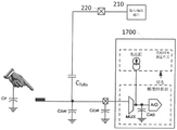
According to various embodiments, as shown, for example, in fig. 6, a Tx drive signal generated, for example, by an I/O port 210 of the microcontroller 110 is added to the circuit via an external connection 220. To this end, second electrodes 250, 260, 270 may be provided as shown in fig. 7 a-c. For example, as shown in fig. 7c, the second electrode 270 may, for example, surround the sensor electrode 150 as a shield or guard. However, the placement of the second electrode is not critical, and it need only be ensured that the capacitive coupling between the guard or shield electrode 250, 260, 270 and the sensor electrode 150 is greater than the capacitive coupling between the guard or shield electrode 250, 260, 270 and the plate's ground 170. Thus, according to one embodiment, shield electrode 260 and sensor electrode 150 may be formed in different layers, for example, layers of a printed circuit board as shown in fig. 7 b. Any other arrangement of electrodes is possible. For example, FIG. 7a shows an embodiment with shield electrode 250 only partially surrounding sensor electrode 150. Many other ways of capacitive coupling for the signals produced by the ports 210 are possible. FIG. 6 shows that the output signal from the microcontroller, referred to as "Tx", is now added to the circuit via capacitive coupling.
In addition, FIG. 6 also shows an example, various switches 610-660 allowing separate charging of external and internal capacitors with VDD or ground. The switch 660 may not be necessary if the ADC 160 has a high impedance input. Elements 670 and 680 and their function will be explained below with reference to fig. 18. The switch may be automatically controlled by a state machine associated with the CVD unit. For a better overview, fig. 8 and 10-13 do not show switches.
FIG. 8 shows the definition of "mutual capacitance" with reference numeral 125. Fig. 8 shows AC coupling between the sensor 150 and the "Tx" (referred to as "protection" or "shielding") drive signal provided by the port 210 via the external connection 220. CTxRx represents the AC coupling between the low impedance TX signal and the high impedance sensor 150. In other words, pin 220 is an output pin and pin 130 is an input pin. As the Tx signal moves, charge will penetrate into the Rx sensor 150. The amount of AC coupling between the TX drive and the sensor 150 is referred to as the mutual capacitance and is represented by CTxRx or reference numeral 125.
FIG. 9 shows, in a similar manner as FIG. 3, timing diagrams of measurement and drive signals according to various embodiments. In particular, fig. 9 shows how TX signal 900 is driven with a CVD waveform. The measurement cycle begins at time t1 in the same manner as shown in fig. 3. After the first settled phase has started at time t2, the TX signal is driven high at time t 2'. The TX node 220 couples charge into the RX sensor 150 to make the final settling point higher than before. At time t4, the second measurement again begins a reverse charge similar to that in fig. 3. After the second settled phase has begun at time t5, TX signal 900 is driven low at time t 5'. TX node 220 couples charge into RX sensor 150 to bring the final settling point below that before. If the mutual capacitance is reduced, the offset caused by TX signal 900 will be reduced. The effect will be a shift in the final settling voltage in the opposite direction to the TX drive. This will be in the same direction as when the self-capacitance is reduced. If the mutual capacitance increases, the offset caused by the TX signal will increase. This will be in the opposite direction as when the self-capacitance increases.
The drive signal 900 is driven in phase with the CVD waveform, but after the sensor has been set to a high impedance input and settled at the voltage between the internal and external capacitors. Timing (e.g., the difference between t2 and t2 'or between t5 and t 5') is not critical, and the rising edge of the pulse may begin at any time after high impedance settling is available. Thus, the pulse may occur as early as when high impedance is available (e.g., t 2-t 2 'and t 5-t 5'), or even after reaching the settling time (t3 and t6), depending on the time difference of the process, this will require additional settling time for pulse charging. As shown in fig. 9, short time differences t2 '> t2 and t 5' > t5 may be used according to various embodiments. As indicated, the same timing requirements may apply to the rising and falling edges of pulse 900. However, as timing is not critical, different time differences between t2 and t2 'and between t5 and t 5' may be applied according to some embodiments.
During the first portion of the CVD waveforms t 1-t 3, the TX drive 900 will be coupled into the sensor and the final settled voltage higher than it would be without TX coupling. During the second portion of the CVD waveforms t 4-t 6, the TX drive 900 will be coupled into the sensor and the final settled voltage is lower than it would be without TX coupling. An increase in the mutual coupling 125 between TX and sensor 150 will increase this effect.
The principle of adding mutual capacitance charge according to various embodiments is not limited to the capacitive voltage divider measurement method shown. It is also applicable to other capacitance measurements as long as there is a high impedance measurement allowing charging of the sensor 150 via the capacitive coupling 125 between the shield/ guard electrodes 250, 260, 270 and the sensor electrode 150. As mentioned above, the principles according to various embodiments may also be applied, for example, to Charge Time Measurement Units (CTMUs) available in many microcontrollers made by the applicant.
Fig. 10 shows how contaminants, such as water 1000, are coupled into Tx drive (CTxF), sensor (CFRx), and ground of the board (CFGnd), according to various embodiments. The presence of water 1000 slightly reduces CTxRx because it redirects some of the charge away from the sensor 150 and into the water 1000. The plate may be designed such that CFRx is much larger than CFGnd. This may be accomplished, for example, by simply moving the ground away from the sensor 150. When water 1000 is added to the circuit, it is coupled to the TX drive pin 220, the sensor 150, and the ground 170 of the board.
Fig. 11 shows that as CFRx > CFGnd, charge traveling through CTxF is redirected through CFRx to sensor 150. Water 1000 will reduce CTXRX and redirect charge through CTXF. According to an embodiment, the board has been designed such that CFRX is larger than CFGND. The charge in the water 1000 is now redirected into the CFRX. Water 1000 reduces CTXRX but redirects the charge back into sensor 150 through another path. The overall effect is an increase in the mutual capacitance between TX and sensor 150.
Although CTxRx is reduced by water 1000, the CTxF to CFRx path causes an overall increase in coupling between Tx and Rx. Thus, the mutual capacitance between the shield/ guard electrodes 250, 260, 270 and the sensor 150 increases when water 1000 is added to the circuit.
If CFRx < CFgnd, charge traveling through CTxF will be redirected through CFgnd into the ground 170 of the plate. This will result in a reduction of the coupling between Tx and Rx. Thus, the mutual capacitance will decrease. This is the opposite behavior to that previously described, and the ability to distinguish ungrounded conductive objects from grounded conductive objects for this method is catastrophic. The difference in the shift direction of the mutually coupled signals is essential for a correct application of this method.
Likewise, it must be remembered that the self-capacitance increases due to the parallel CFRx-to-CFGnd coupling paths. Thus, the water 1000 increases the self capacitance and increases the mutual capacitance.
Fig. 12 again shows finger 1200 coupled to the circuit in the same manner as water 1000, except that the CHBM-to-CGndGnd coupling path exists. The presence of the finger 1200 slightly reduces CTxRx because it redirects some charge away from the sensor 150 and into the finger 1200.
When the user's finger 1200 is added to the circuit, it couples into the Tx drive, sensor 150 and the board's ground 170, but there is now also a coupling path into the ground through the user's human finger model and then some amount of coupling between the ground and the board's ground.
As shown in fig. 13, if CGndGnd is not open, the Tx charge will be redirected into the ground 170 of the plate. CTXRX decreases as some of the TX charge is redirected into the sensor. However, unlike water, due to the CHBM path being larger than CFRX, the charge now travels down through the CHBM path and into the ground 170 of the plate. The result is that the finger will reduce the mutual capacitance between the shield/ shield 250, 260, 270 and the sensor 150, which can be considered equivalent to the opposite behavior of water. If CGndgnd is open, then the TX charge will behave in the same way as water. The CHBM path has no effect. The result is that the finger 1200 will increase the mutual capacitance, which is considered disadvantageous because it behaves the same as water.
Likewise, according to the general principles of various embodiments, it must be remembered that self-capacitance is due to CFRxTo CFGndPath and CFRxTo CHBMTo CGndGndThe path increases. Thus, water or any other ungrounded contaminant increases the self-capacitance and increases the mutual capacitance, and any other grounded contaminant increases the self-capacitance and decreases the mutual capacitance.
FIG. 14 shows a timing diagram of the signal output of the same sensor scanned in three ways simultaneously: only self-capacitance 120 is shown with signal 1410. Here, the TX line is not driven, so there is no AC coupling. Only the mutual capacitance 125 is shown with a signal 1420. Here, 'charge sharing' of the CVD waveform is not performed, but the TX line is driven. This results in AC-only coupling. Finally, signal 1430 shows the results when the two self-capacitance and mutual capacitance measurements shown in FIG. 9 are performed simultaneously. In other words, CVD is performed and the TX lines are driven.
Fig. 14 shows the output signal of the ADC for the first measurement (in other words, the measurement effected at time t3 in fig. 9). Two user compression events are shown along the timeline, with the first half being a measurement of the "clean" sensor and water added at about the middle of the graph and the second compression event occurring. Thus, the left half of the timing diagram in fig. 14 shows measurements without ungrounded contaminants, where the right half shows similar measurements with ungrounded contaminants (e.g., water). In general, when water is added, for the first measurement of the CVD waveform, as shown in the right half with signal 1410, the increase in self-capacitance decreases the signal. When water is added, as shown in the right half, the increase in mutual capacitance increases the signal 1420.
When a finger is pressed on the cleaning system: self-capacitance 120 increases, dropping the final settled voltage t 3. The mutual capacitance 125 decreases, decreasing the final settled voltage. The combined effect is a large negative shift in the settled voltage.
When water is added to the system as shown in the center of fig. 14, the self-capacitance 120 increases and the mutual capacitance 125 decreases. Due to the design in how signal 900 is driven, it shifts in the opposite direction. The combination of the two effects will thus cancel the output signal and produce substantially no or only a small amount of shift. This results in a water resistance at analog levels according to various embodiments.
When a finger is pressed on the sensor in the presence of water as shown on the right side of fig. 14: the self-capacitance 120 increases due to the extra parallel capacitance of the phantom, causing the final settled voltage 1410 to drop slightly. The water is now charged by the finger and the mutual capacitance 125 is reduced as the TX charge is directed to ground. This causes the final settled voltage 1420 to drop significantly. The combined effect 1430 is a large negative displacement similar to a press in a dry environment.
Fig. 15 shows a second measurement identical to fig. 14, but now for the CVD measurement, in other words the measurement performed at time t6 in fig. 9. Thus, the signal form is substantially reversed from that shown in fig. 14, and signal 1510 corresponds to signal 1410, signal 1520 corresponds to 1420, and signal 1530 corresponds to signal 1430. For a second measurement in the CVD measurements, an increase in self-capacitance increases the signal and an increase in mutual capacitance decreases the signal. Thus, the directions are different, but the behavior is the same as the signals in fig. 14.
Thus, in general, as long as the self-and mutual capacitances are differential with respect to ungrounded objects and non-differential with respect to grounded objects, their precise varying behavior does not matter, according to various embodiments.
Fig. 16 shows the final output signal processed by subtracting the first measurement signal 1430 from the second measurement signal 1530. The water resistance is ensured at the signal/analog level. No software decoding is required, and no pattern recognition and additional filtering are required. Signal displacement occurs due to a finger or grounded conductive object, but is eliminated when water or conductive objects are not grounded.
As mentioned above, other measurement units may be used. Fig. 17 shows a charge time measurement unit, for example, integrated into a microcontroller 1700 that can be used to measure capacitance. For example, in a touch application with a total capacitance including parasitic elements such as a 30pF switch (CSW) and circuit (CCIR) as shown in fig. 17, when the external circuit is charged with a constant current of, for example, 5.5 μ Α for 10 μ s, this results in a voltage of 1.83V. When a touch of a finger is added, an additional Capacitance (CF) of up to 10pF is added. The exact amount of capacitance depends on how much the touch pad is covered by the finger and any covering material over the pad. For the 10pF change, where the current and charge time are the same, the voltage is 1.38V. The voltage is measured at frequency intervals by the a/D converter of the microcontroller. Then, the change (especially a decrease) may be interpreted as a touch event. During charging of the external capacitor, a high impedance input is established and a mutual capacitance measurement may be performed.
When the self-capacitance and mutual capacitance of the circuit are equal, their behavior can be combined as described above to eliminate the effect of ungrounded conductive objects on the capacitive sensor. The effectiveness of this solution is significantly reduced if the self and mutual capacitances of the circuit are not equal. Thus, as shown in fig. 18, according to another embodiment, similar results as described above may be achieved with individual measurements combined by software. Scaling can then be performed in software to further improve the measurement. For purposes of equalization, the relative change in the "mutual capacitance" measurement may be proportional to the relative change in the "self capacitance" measurement, according to some embodiments. If the mutual and self capacitances are not equal, their signals can be taken separately (as they have done) to account for the combined measurements and emphasize their behavior to make them equal. Thus, a simple function can be performed in software to scale the effect of the 'mutual capacitance' measurement to the effect of the 'self capacitance' measurement. However, this would require some processing and longer measurements, since two separate measurements are necessary, and scaling of one measurement and combining of the two self-and mutual capacitance measurements is also necessary.
Alternatively, according to other embodiments, a calibration routine may be performed in which results of individual measurements are determined and measurement parameters are adjusted to scale the results. Once this has been done, a combined measurement as described above may be performed, wherein the voltage levels are now adapted according to a calibration routine. Thus, during calibration, each capacitance measurement is performed individually. For example, the self-capacitance is first measured and then under the same conditions, the mutual capacitance measurement is performed. According to some embodiments, the average of each measurement may be processed and then an equalization factor may be calculated. According to one embodiment, the voltage or other corresponding parameter is adjusted in the loop until the scaling reaches the correct output value, in other words, until the output data of the self-capacitance measurement is approximately equal to the output data of the mutual capacitance measurement. Then, depending on how the factor is determined, this factor may be applied to either the mutual capacitance measurement or the self-capacitance measurement. In other words, the charging signal or pulse signal amplitude is adjusted by a scaling factor to optimize the combined self-capacitance and mutual capacitance measurements. Once this has been performed, touch detection may be performed using combinatorial techniques.
To this end, pulses for mutual capacitance measurements may be generated using, for example, a digital-to-analog converter (DAC)670 and I/O port 210 as shown in dashed lines in an alternative embodiment in FIG. 6. According to some embodiments, the output voltage of the DAC 670 may be varied according to a scaling factor. Alternatively, the charging voltage for the self capacitance measurement may be provided by the reference voltage generator or DAC 680 may be programmed without using VDD. This is also shown in fig. 6 using dashed lines as an alternative embodiment. Thus, according to some embodiments, the reference voltage and/or the pulsed output voltage for charging may be changed according to a calculated scaling factor.
This is again applicable to any type of capacitance measurement using a high impedance input. However, other factors may be varied with respect to the particular measurement technique. For example, the time or constant current value, or both, may be adjusted relative to the charge time measurement unit. Which parameter is changed therefore depends on the respective measurement technique. In general, the respective self-capacitance and mutual capacitance signals may be scaled in software to equalize their magnitudes, then combined to generate one sensor output signal according to some embodiments.
Claims (18)
1. A method for performing touch determination with a capacitive sensor;
initiating a self-capacitance measurement of a capacitive sensor electrode coupled with an input of a measurement circuit, wherein a mutual capacitance measurement comprising the capacitive sensor electrode and a second electrode adjacent to the capacitive sensor electrode is performed simultaneously, wherein after the input has been set to a high impedance state during the self-capacitance measurement, a separate pulse is generated by an output port of the measurement circuit and the pulse is capacitively coupled into the capacitive sensor electrode via the second electrode to perform the mutual capacitance measurement.
2. The method of claim 1, wherein the self-capacitance measurement is a capacitive voltage divider measurement.
3. The method of claim 1, wherein the self-capacitance measurement is a charge time measurement.
4. The method of claim 1, further comprising a calibration method, wherein the calibration method is performed prior to performing touch determination, the calibration method comprising:
performing individual self-capacitance measurements and storing a first measurement value;
performing individual mutual capacitance measurements and storing a second measurement value; and
calculating a scaling factor from the first and second measurements;
wherein the method for performing touch determination includes applying the scaling factor to the self capacitance or the mutual capacitance measurement.
5. A method according to any one of the preceding claims,
wherein the first self-capacitance and mutual capacitance measurements are performed by:
charging a first capacitor of the measurement circuit to a first level and a second capacitor formed by the capacitive sensor electrode to a second level;
coupling a first capacitor and a second capacitor in parallel while setting the input to a high impedance and feeding a pulse generated by an I/O port and having the first level to a guard electrode capacitively coupled with the second capacitor;
determining a first settled voltage level of the parallel coupled capacitors after a settling phase;
thereafter performing a second self-capacitance and mutual capacitance measurement by:
charging the first capacitor to the second level and charging the second capacitor to the first level;
coupling the first capacitor and a second capacitor in parallel while setting the input to a high impedance, wherein the pulse is terminated upon coupling of the first and second capacitors;
after settling the phase, determining a second settled voltage level of the parallel coupled capacitors.
6. The method of claim 5, wherein the first voltage level is a predetermined voltage VDDAnd the second voltage level is a ground level VSS。
7. The method of claim 5, wherein the second voltage level is a predetermined voltage VDDAnd the first voltage level is a ground level VSS。
8. The method of claim 5, wherein the pulse has a voltage level VDDAnd begins after expiration of a predetermined period of time that begins when the first and second capacitors are coupled in parallel.
9. A microcontroller for performing touch determination with a capacitive sensor, comprising:
a capacitance measurement unit configurable to perform a self-capacitance measurement in combination with a mutual capacitance measurement and comprising a control unit operable to:
initiating a self-capacitance measurement of a capacitive sensor electrode coupled with an input of the capacitive measurement unit, wherein a mutual capacitance measurement including the capacitive sensor electrode and a second electrode adjacent to the capacitive sensor electrode is performed simultaneously, wherein the capacitive measurement unit is configured to switch the input to a high impedance state and generate a separate pulse through an output port of the capacitive measurement unit during the self-capacitance measurement and capacitively couple the pulse into the capacitive sensor electrode via the second electrode to perform the mutual capacitance measurement.
10. The microcontroller according to claim 9, wherein the capacitance measurement unit comprises a capacitive divider measurement unit.
11. The microcontroller according to claim 10, wherein the capacitive voltage divider measurement unit comprises:
a first switching unit coupled between a first external pin and a sample and hold capacitor forming a first capacitor and operable to charge a second capacitor to a first or second voltage level or switch an externally connected capacitor in parallel with the sample and hold capacitor;
a second switching unit coupled with the sample and hold capacitor and operable to charge the sample and hold capacitor to the first or the second voltage level;
an analog-to-digital converter operable to couple with the parallel-switched capacitor; and is
Wherein the control unit is configured to control the first and the second switching units.
12. The microcontroller according to claim 11, further comprising a second external pin coupled with an input/output port configurable to operate as an output port, wherein the control unit is configured to control the output port for generating the independent pulses.
13. The microcontroller according to claim 9, wherein the capacitance measurement unit comprises a charge time measurement, wherein the control unit is configured to control a self-capacitance measurement with the charge time measurement unit, wherein the charge time measurement unit is connected with a first external pin adapted to be connected with a capacitance sensor electrode.
14. The microcontroller according to claim 13, further comprising a second external pin coupled with an input/output port configurable to operate as an output port, wherein the control unit is configured to control the output port for generating the independent pulses.
15. The microcontroller according to claim 9, wherein the control unit is configured to perform calibration before performing touch determination, the control unit controlling:
individual self-capacitance measurements and storing a first measurement value;
individual mutual capacitance measurements and storing a second measurement value; and is
Wherein a processor of the control unit or the microcontroller is configured to calculate a scaling factor from the first and the second measurements;
wherein for performing a touch determination, the control unit is configured to apply the scaling factor to the self capacitance or the mutual capacitance measurement.
16. The microcontroller according to claim 15, wherein the scaling factor changes a charge level during the self-capacitance measurement or changes a voltage level during the mutual capacitance measurement.
17. A system comprising the microcontroller according to claim 12, comprising the capacitive sensor electrode connected with the microcontroller through the first external pin and a shield or guard electrode arranged proximate the capacitive sensor electrode connected with the second external pin.
18. A system comprising the microcontroller according to claim 14, comprising the capacitive sensor connected with the microcontroller through the first external pin and a shield or guard electrode arranged proximate the capacitive sensor connected with the second external pin.
Applications Claiming Priority (5)
| Application Number | Priority Date | Filing Date | Title |
|---|---|---|---|
| US201462068450P | 2014-10-24 | 2014-10-24 | |
| US62/068,450 | 2014-10-24 | ||
| US14/566,183 | 2014-12-10 | ||
| US14/566,183 US9542051B2 (en) | 2014-10-24 | 2014-12-10 | Analog elimination of ungrounded conductive objects in capacitive sensing |
| PCT/US2015/013057 WO2016064438A1 (en) | 2014-10-24 | 2015-01-27 | Analog elimination of ungrounded conductive objects in capacitive sensing |
Publications (2)
| Publication Number | Publication Date |
|---|---|
| CN106716839A CN106716839A (en) | 2017-05-24 |
| CN106716839B true CN106716839B (en) | 2021-03-23 |
Family
ID=52472596
Family Applications (1)
| Application Number | Title | Priority Date | Filing Date |
|---|---|---|---|
| CN201580052185.3A Active CN106716839B (en) | 2014-10-24 | 2015-01-27 | Analog cancellation of ungrounded conductive objects in capacitive sensing |
Country Status (7)
| Country | Link |
|---|---|
| US (2) | US9542051B2 (en) |
| EP (2) | EP3331165B1 (en) |
| JP (1) | JP6606175B2 (en) |
| KR (2) | KR102253923B1 (en) |
| CN (1) | CN106716839B (en) |
| TW (2) | TWI640911B (en) |
| WO (1) | WO2016064438A1 (en) |
Families Citing this family (31)
| Publication number | Priority date | Publication date | Assignee | Title |
|---|---|---|---|---|
| LU92582B1 (en) * | 2014-10-22 | 2016-04-25 | Iee Sarl | Low-cost complex impedance measurement circuit for guardsense capacitive sensors operated in loading mode |
| US9542051B2 (en) | 2014-10-24 | 2017-01-10 | Microchip Technology Incorporated | Analog elimination of ungrounded conductive objects in capacitive sensing |
| KR102382999B1 (en) | 2015-01-08 | 2022-04-05 | 삼성디스플레이 주식회사 | Display device including touch sensor |
| TWI543060B (en) | 2015-07-21 | 2016-07-21 | 矽創電子股份有限公司 | Calibration method and capacitive sensing device |
| US10444892B2 (en) * | 2015-10-07 | 2019-10-15 | Microchip Technology Incorporated | Capacitance measurement device with reduced noise |
| KR20180013559A (en) * | 2016-07-29 | 2018-02-07 | 엘에스오토모티브 주식회사 | Electrostatic capacity switching unit |
| CN108631762A (en) * | 2017-03-15 | 2018-10-09 | 台湾类比科技股份有限公司 | Touch-control system for waterproof |
| WO2018183732A1 (en) * | 2017-03-29 | 2018-10-04 | Alps Electric Co. Ltd. | Water rejection on capacitive door handle |
| CN106992774B (en) * | 2017-04-18 | 2023-06-02 | 深圳和家园网络科技有限公司 | Human body induction sensor circuit |
| US11442586B2 (en) * | 2017-05-19 | 2022-09-13 | Microchip Technology Incorporated | Canceling unwanted capacitive effects in a capacitive touch measurement, and related systems, methods, and devices |
| TW201901398A (en) | 2017-05-19 | 2019-01-01 | 美商愛特梅爾公司 | Technique for eliminating undesired capacitive effects in a capacitive touch interface, and related systems, methods, and devices |
| DE102017111253B4 (en) * | 2017-05-23 | 2020-10-01 | Preh Gmbh | Method for capacitive touch and actuation detection |
| US10558306B2 (en) * | 2017-06-12 | 2020-02-11 | Himax Technologies Limited | In-cell touch apparatus and a water mode detection method thereof |
| US11075633B2 (en) * | 2017-06-13 | 2021-07-27 | Semtech Corporation | Water-rejection proximity detector and method |
| US10146390B1 (en) * | 2017-07-21 | 2018-12-04 | Cypress Semiconductor Corporation | Method of combining self and mutual capacitance sensing |
| US10572087B2 (en) * | 2017-07-27 | 2020-02-25 | Cirque Corporation | Self-capacitence sensor and sensor array sensitivity calibration method using secondary mutual capacitence measurements |
| JP6392420B1 (en) * | 2017-07-28 | 2018-09-19 | エルエス オートモーティブ テクノロジーズ カンパニー リミテッドLs Automotive Technologies Co., Ltd. | Capacitance switch unit and manufacturing method thereof |
| FR3070706B1 (en) * | 2017-09-05 | 2019-08-23 | Continental Automotive France | DEVICE FOR DETECTING INTENTION OF LOCKING OR UNLOCKING A VEHICLE OF A MOTOR VEHICLE BY A USER AND ASSOCIATED DOOR HANDLE |
| CN109814762B (en) * | 2017-11-22 | 2022-05-03 | 矽统科技股份有限公司 | Touch detection circuit and method |
| TWI635433B (en) * | 2017-11-22 | 2018-09-11 | 矽統科技股份有限公司 | Circuit and method for touch sensing |
| US10545614B2 (en) | 2018-01-22 | 2020-01-28 | Cypress Semiconductor Corporation | Two-electrode touch button with a multi-phase capacitance measurement process |
| US10698540B2 (en) | 2018-01-22 | 2020-06-30 | Semicondutor Components Industries, Llc | Methods and apparatus for a capacitive touch sensor |
| FR3077449B1 (en) * | 2018-01-29 | 2021-01-08 | Continental Automotive France | METHOD AND DEVICE FOR PRESENCE DETECTION WITH MULTIPLE DETECTION ZONES FOR MOTOR VEHICLES |
| US10901551B2 (en) * | 2018-03-01 | 2021-01-26 | Microchip Technology Incorporated | Method and system for touchless gesture detection and hover and touch detection |
| JP7068890B2 (en) * | 2018-03-30 | 2022-05-17 | 株式会社デンソーテン | Electrostatic input device |
| DE102020110172A1 (en) * | 2020-04-14 | 2021-10-14 | Preh Gmbh | Method for capacitive touch and actuation detection |
| JP7445523B2 (en) * | 2020-06-04 | 2024-03-07 | ホシデン株式会社 | capacitive sensor |
| WO2022016359A1 (en) * | 2020-07-21 | 2022-01-27 | 深圳市汇顶科技股份有限公司 | Capacitance detection circuit, and touch chip |
| FR3123525B1 (en) * | 2021-05-25 | 2023-04-14 | Vitesco Technologies | Capacitive proximity sensor |
| DE102022104117A1 (en) | 2022-02-22 | 2023-08-24 | Valeo Schalter Und Sensoren Gmbh | Method for determining a manual actuation of a capacitive sensor element, evaluation unit therefor and sensor device |
| EP4270789A1 (en) * | 2022-04-27 | 2023-11-01 | NXP USA, Inc. | Capacitive touch sensor |
Citations (2)
| Publication number | Priority date | Publication date | Assignee | Title |
|---|---|---|---|---|
| CN102273076A (en) * | 2009-01-12 | 2011-12-07 | 密克罗奇普技术公司 | Capacitive touch sensing and light emitting diode drive matrix |
| CN103918183A (en) * | 2011-10-07 | 2014-07-09 | 密克罗奇普技术公司 | Measuring capacitance of a capacitive sensor with a microcontroller having an analog output for driving a guard ring |
Family Cites Families (16)
| Publication number | Priority date | Publication date | Assignee | Title |
|---|---|---|---|---|
| US8493331B2 (en) * | 2007-06-13 | 2013-07-23 | Apple Inc. | Touch detection using multiple simultaneous frequencies |
| US8810542B2 (en) * | 2008-09-10 | 2014-08-19 | Apple Inc. | Correction of parasitic capacitance effect in touch sensor panels |
| WO2010036545A2 (en) * | 2008-09-24 | 2010-04-01 | 3M Innovative Properties Company | Mutual capacitance measuring circuits and methods |
| JP5369888B2 (en) * | 2009-05-19 | 2013-12-18 | トヨタ紡織株式会社 | Electrode structure of capacitance sensor and vehicle proximity sensor using the same |
| CN102460357B (en) * | 2009-05-29 | 2016-04-27 | 3M创新有限公司 | High-speed multi-drop touch-control touching device and controller thereof |
| US9069405B2 (en) * | 2009-07-28 | 2015-06-30 | Cypress Semiconductor Corporation | Dynamic mode switching for fast touch response |
| US8339286B2 (en) * | 2010-03-31 | 2012-12-25 | 3M Innovative Properties Company | Baseline update procedure for touch sensitive device |
| US8773146B1 (en) * | 2010-04-16 | 2014-07-08 | Cypress Semiconductor Corporation | Waterproof scanning of a capacitive sense array |
| US8933907B2 (en) * | 2010-04-30 | 2015-01-13 | Microchip Technology Incorporated | Capacitive touch system using both self and mutual capacitance |
| US20120026123A1 (en) * | 2010-07-30 | 2012-02-02 | Grunthaner Martin Paul | Compensation for Capacitance Change in Touch Sensing Device |
| US9268441B2 (en) * | 2011-04-05 | 2016-02-23 | Parade Technologies, Ltd. | Active integrator for a capacitive sense array |
| US9086768B2 (en) * | 2012-04-30 | 2015-07-21 | Apple Inc. | Mitigation of parasitic capacitance |
| US9116572B2 (en) * | 2013-04-15 | 2015-08-25 | Apple Inc. | Disambiguation of touch input events on a touch sensor panel |
| US8823399B1 (en) * | 2013-10-07 | 2014-09-02 | Cypress Semiconductor Corporation | Detect and differentiate touches from different size conductive objects on a capacitive button |
| US9965108B2 (en) * | 2014-05-16 | 2018-05-08 | Apple Inc. | Simultaneous self- and mutual capacitance sensing |
| US9542051B2 (en) | 2014-10-24 | 2017-01-10 | Microchip Technology Incorporated | Analog elimination of ungrounded conductive objects in capacitive sensing |
-
2014
- 2014-12-10 US US14/566,183 patent/US9542051B2/en active Active
-
2015
- 2015-01-27 WO PCT/US2015/013057 patent/WO2016064438A1/en active Application Filing
- 2015-01-27 EP EP18152429.9A patent/EP3331165B1/en active Active
- 2015-01-27 CN CN201580052185.3A patent/CN106716839B/en active Active
- 2015-01-27 EP EP15704639.2A patent/EP3210305B1/en active Active
- 2015-01-27 KR KR1020177008388A patent/KR102253923B1/en active IP Right Grant
- 2015-01-27 KR KR1020217009464A patent/KR102325699B1/en active IP Right Grant
- 2015-01-27 JP JP2017511905A patent/JP6606175B2/en active Active
- 2015-02-02 TW TW104103464A patent/TWI640911B/en active
- 2015-02-02 TW TW107134083A patent/TWI681327B/en active
-
2017
- 2017-01-09 US US15/401,593 patent/US10191591B2/en active Active
Patent Citations (2)
| Publication number | Priority date | Publication date | Assignee | Title |
|---|---|---|---|---|
| CN102273076A (en) * | 2009-01-12 | 2011-12-07 | 密克罗奇普技术公司 | Capacitive touch sensing and light emitting diode drive matrix |
| CN103918183A (en) * | 2011-10-07 | 2014-07-09 | 密克罗奇普技术公司 | Measuring capacitance of a capacitive sensor with a microcontroller having an analog output for driving a guard ring |
Also Published As
| Publication number | Publication date |
|---|---|
| WO2016064438A1 (en) | 2016-04-28 |
| KR20210040459A (en) | 2021-04-13 |
| EP3210305A1 (en) | 2017-08-30 |
| JP2018502464A (en) | 2018-01-25 |
| EP3331165B1 (en) | 2020-07-29 |
| TW201616326A (en) | 2016-05-01 |
| KR102325699B1 (en) | 2021-11-15 |
| EP3331165A1 (en) | 2018-06-06 |
| TW201903591A (en) | 2019-01-16 |
| CN106716839A (en) | 2017-05-24 |
| US20170139540A1 (en) | 2017-05-18 |
| KR102253923B1 (en) | 2021-05-21 |
| US20160117014A1 (en) | 2016-04-28 |
| KR20170072190A (en) | 2017-06-26 |
| US10191591B2 (en) | 2019-01-29 |
| JP6606175B2 (en) | 2019-11-13 |
| TWI640911B (en) | 2018-11-11 |
| US9542051B2 (en) | 2017-01-10 |
| EP3210305B1 (en) | 2019-08-07 |
| TWI681327B (en) | 2020-01-01 |
Similar Documents
| Publication | Publication Date | Title |
|---|---|---|
| CN106716839B (en) | Analog cancellation of ungrounded conductive objects in capacitive sensing | |
| KR101872368B1 (en) | Capacitive fingerprint sensing device with demodulation circuitry in sensing element | |
| US8866500B2 (en) | Multi-functional capacitance sensing circuit with a current conveyor | |
| US10003334B2 (en) | Capacitative sensor system | |
| US10790822B2 (en) | Switching arrangement and method for a capacitive sensor | |
| CN110383221A (en) | Input unit and its control method | |
| US9019236B2 (en) | Capacitive touch pad configured for proximity detection | |
| US20140039819A1 (en) | Method and apparatus to measure self-capacitance using a single pin | |
| US8952927B2 (en) | Self-capacitance measurement with compensated capacitance | |
| US20120182252A1 (en) | Differential Capacitive Touchscreen or Touch Panel | |
| US9921691B2 (en) | Burst-mode self-capacitance measurement with compensated capacitance | |
| CN109313515B (en) | Touch sensitive display device | |
| US20160092019A1 (en) | Scanning method and device of a single layer capacitive touch panel | |
| CN110050253B (en) | Multi-stage self-capacitance scanning of sensor arrays | |
| US20120286809A1 (en) | Circuit Arrangement for Determining a Capacitance of a Number of Capacitive Sensor Elements | |
| KR101625103B1 (en) | Touch screen device and driving method for sensing multi touch | |
| TWI559232B (en) | Sensing method and circuit of fingerprint sensor | |
| Oballe-Peinado et al. | Direct interfaces for smart skins based on FPGAs | |
| KR20180097242A (en) | Detection Method of Capacitance and Capacitance Detection Apparatus using the Same | |
| KR20150087754A (en) | Touch sensor and driving method for sensing multi touch |
Legal Events
| Date | Code | Title | Description |
|---|---|---|---|
| PB01 | Publication | ||
| PB01 | Publication | ||
| SE01 | Entry into force of request for substantive examination | ||
| SE01 | Entry into force of request for substantive examination | ||
| GR01 | Patent grant | ||
| GR01 | Patent grant |