CN106340319B - Method and circuit for protecting and verifying address data - Google Patents
Method and circuit for protecting and verifying address data Download PDFInfo
- Publication number
- CN106340319B CN106340319B CN201610108842.8A CN201610108842A CN106340319B CN 106340319 B CN106340319 B CN 106340319B CN 201610108842 A CN201610108842 A CN 201610108842A CN 106340319 B CN106340319 B CN 106340319B
- Authority
- CN
- China
- Prior art keywords
- address
- data
- write
- circuit
- bus
- Prior art date
- Legal status (The legal status is an assumption and is not a legal conclusion. Google has not performed a legal analysis and makes no representation as to the accuracy of the status listed.)
- Active
Links
Images


Classifications
-
- G—PHYSICS
- G06—COMPUTING; CALCULATING OR COUNTING
- G06F—ELECTRIC DIGITAL DATA PROCESSING
- G06F12/00—Accessing, addressing or allocating within memory systems or architectures
- G06F12/14—Protection against unauthorised use of memory or access to memory
- G06F12/1416—Protection against unauthorised use of memory or access to memory by checking the object accessibility, e.g. type of access defined by the memory independently of subject rights
- G06F12/145—Protection against unauthorised use of memory or access to memory by checking the object accessibility, e.g. type of access defined by the memory independently of subject rights the protection being virtual, e.g. for virtual blocks or segments before a translation mechanism
-
- G—PHYSICS
- G11—INFORMATION STORAGE
- G11C—STATIC STORES
- G11C7/00—Arrangements for writing information into, or reading information out from, a digital store
- G11C7/24—Memory cell safety or protection circuits, e.g. arrangements for preventing inadvertent reading or writing; Status cells; Test cells
-
- G—PHYSICS
- G06—COMPUTING; CALCULATING OR COUNTING
- G06F—ELECTRIC DIGITAL DATA PROCESSING
- G06F11/00—Error detection; Error correction; Monitoring
- G06F11/07—Responding to the occurrence of a fault, e.g. fault tolerance
- G06F11/08—Error detection or correction by redundancy in data representation, e.g. by using checking codes
- G06F11/10—Adding special bits or symbols to the coded information, e.g. parity check, casting out 9's or 11's
- G06F11/1008—Adding special bits or symbols to the coded information, e.g. parity check, casting out 9's or 11's in individual solid state devices
- G06F11/1012—Adding special bits or symbols to the coded information, e.g. parity check, casting out 9's or 11's in individual solid state devices using codes or arrangements adapted for a specific type of error
- G06F11/1016—Error in accessing a memory location, i.e. addressing error
-
- G—PHYSICS
- G06—COMPUTING; CALCULATING OR COUNTING
- G06F—ELECTRIC DIGITAL DATA PROCESSING
- G06F12/00—Accessing, addressing or allocating within memory systems or architectures
- G06F12/14—Protection against unauthorised use of memory or access to memory
- G06F12/1408—Protection against unauthorised use of memory or access to memory by using cryptography
-
- G—PHYSICS
- G06—COMPUTING; CALCULATING OR COUNTING
- G06F—ELECTRIC DIGITAL DATA PROCESSING
- G06F13/00—Interconnection of, or transfer of information or other signals between, memories, input/output devices or central processing units
- G06F13/14—Handling requests for interconnection or transfer
- G06F13/16—Handling requests for interconnection or transfer for access to memory bus
- G06F13/1668—Details of memory controller
- G06F13/1678—Details of memory controller using bus width
-
- G—PHYSICS
- G06—COMPUTING; CALCULATING OR COUNTING
- G06F—ELECTRIC DIGITAL DATA PROCESSING
- G06F13/00—Interconnection of, or transfer of information or other signals between, memories, input/output devices or central processing units
- G06F13/38—Information transfer, e.g. on bus
- G06F13/40—Bus structure
- G06F13/4004—Coupling between buses
- G06F13/4027—Coupling between buses using bus bridges
- G06F13/404—Coupling between buses using bus bridges with address mapping
-
- G—PHYSICS
- G06—COMPUTING; CALCULATING OR COUNTING
- G06F—ELECTRIC DIGITAL DATA PROCESSING
- G06F13/00—Interconnection of, or transfer of information or other signals between, memories, input/output devices or central processing units
- G06F13/38—Information transfer, e.g. on bus
- G06F13/42—Bus transfer protocol, e.g. handshake; Synchronisation
- G06F13/4282—Bus transfer protocol, e.g. handshake; Synchronisation on a serial bus, e.g. I2C bus, SPI bus
-
- G—PHYSICS
- G06—COMPUTING; CALCULATING OR COUNTING
- G06F—ELECTRIC DIGITAL DATA PROCESSING
- G06F3/00—Input arrangements for transferring data to be processed into a form capable of being handled by the computer; Output arrangements for transferring data from processing unit to output unit, e.g. interface arrangements
- G06F3/06—Digital input from, or digital output to, record carriers, e.g. RAID, emulated record carriers or networked record carriers
- G06F3/0601—Interfaces specially adapted for storage systems
- G06F3/0602—Interfaces specially adapted for storage systems specifically adapted to achieve a particular effect
- G06F3/0614—Improving the reliability of storage systems
- G06F3/0619—Improving the reliability of storage systems in relation to data integrity, e.g. data losses, bit errors
-
- G—PHYSICS
- G06—COMPUTING; CALCULATING OR COUNTING
- G06F—ELECTRIC DIGITAL DATA PROCESSING
- G06F3/00—Input arrangements for transferring data to be processed into a form capable of being handled by the computer; Output arrangements for transferring data from processing unit to output unit, e.g. interface arrangements
- G06F3/06—Digital input from, or digital output to, record carriers, e.g. RAID, emulated record carriers or networked record carriers
- G06F3/0601—Interfaces specially adapted for storage systems
- G06F3/0628—Interfaces specially adapted for storage systems making use of a particular technique
- G06F3/0629—Configuration or reconfiguration of storage systems
-
- G—PHYSICS
- G06—COMPUTING; CALCULATING OR COUNTING
- G06F—ELECTRIC DIGITAL DATA PROCESSING
- G06F3/00—Input arrangements for transferring data to be processed into a form capable of being handled by the computer; Output arrangements for transferring data from processing unit to output unit, e.g. interface arrangements
- G06F3/06—Digital input from, or digital output to, record carriers, e.g. RAID, emulated record carriers or networked record carriers
- G06F3/0601—Interfaces specially adapted for storage systems
- G06F3/0668—Interfaces specially adapted for storage systems adopting a particular infrastructure
- G06F3/0671—In-line storage system
- G06F3/0673—Single storage device
-
- G—PHYSICS
- G11—INFORMATION STORAGE
- G11C—STATIC STORES
- G11C11/00—Digital stores characterised by the use of particular electric or magnetic storage elements; Storage elements therefor
- G11C11/21—Digital stores characterised by the use of particular electric or magnetic storage elements; Storage elements therefor using electric elements
- G11C11/34—Digital stores characterised by the use of particular electric or magnetic storage elements; Storage elements therefor using electric elements using semiconductor devices
- G11C11/40—Digital stores characterised by the use of particular electric or magnetic storage elements; Storage elements therefor using electric elements using semiconductor devices using transistors
- G11C11/401—Digital stores characterised by the use of particular electric or magnetic storage elements; Storage elements therefor using electric elements using semiconductor devices using transistors forming cells needing refreshing or charge regeneration, i.e. dynamic cells
- G11C11/4063—Auxiliary circuits, e.g. for addressing, decoding, driving, writing, sensing or timing
- G11C11/407—Auxiliary circuits, e.g. for addressing, decoding, driving, writing, sensing or timing for memory cells of the field-effect type
- G11C11/4078—Safety or protection circuits, e.g. for preventing inadvertent or unauthorised reading or writing; Status cells; Test cells
-
- G—PHYSICS
- G11—INFORMATION STORAGE
- G11C—STATIC STORES
- G11C11/00—Digital stores characterised by the use of particular electric or magnetic storage elements; Storage elements therefor
- G11C11/21—Digital stores characterised by the use of particular electric or magnetic storage elements; Storage elements therefor using electric elements
- G11C11/34—Digital stores characterised by the use of particular electric or magnetic storage elements; Storage elements therefor using electric elements using semiconductor devices
- G11C11/40—Digital stores characterised by the use of particular electric or magnetic storage elements; Storage elements therefor using electric elements using semiconductor devices using transistors
- G11C11/41—Digital stores characterised by the use of particular electric or magnetic storage elements; Storage elements therefor using electric elements using semiconductor devices using transistors forming static cells with positive feedback, i.e. cells not needing refreshing or charge regeneration, e.g. bistable multivibrator or Schmitt trigger
- G11C11/412—Digital stores characterised by the use of particular electric or magnetic storage elements; Storage elements therefor using electric elements using semiconductor devices using transistors forming static cells with positive feedback, i.e. cells not needing refreshing or charge regeneration, e.g. bistable multivibrator or Schmitt trigger using field-effect transistors only
- G11C11/4125—Cells incorporating circuit means for protecting against loss of information
-
- G—PHYSICS
- G06—COMPUTING; CALCULATING OR COUNTING
- G06F—ELECTRIC DIGITAL DATA PROCESSING
- G06F2212/00—Indexing scheme relating to accessing, addressing or allocation within memory systems or architectures
- G06F2212/10—Providing a specific technical effect
- G06F2212/1052—Security improvement
Abstract
Methods and circuits for protecting and verifying address data are presented. The invention relates to a circuit for protecting memory address data, the circuit being adapted to: receiving write data to be written to the memory device (104) on an input data bus (126) and a corresponding write address on an address bus (122); generating an address protection value based on the write address; and generating modified write data (WRITE DATA') on the output data bus (128), the modified write data including the write data and the address protection value, wherein a width of the output data bus (128) is greater than a width of the input data bus.
Description
Cross Reference to Related Applications
This application claims priority to french patent application No. 15/56621 filed on 10/7/2015, the entire contents of which are incorporated herein by reference to the maximum extent allowed by law.
Technical Field
The present disclosure relates to the field of memory interfaces, and in particular to memory interfaces providing methods and circuits for protecting and verifying address data.
Background
When writing to any memory device, such as a DRAM (dynamic random access memory) or SRAM (static random access memory) device, the signals passed to the memory through the input and/or output lines may be corrupted, for example, as a result of a single event upset.
Although memory interfaces typically include protection and/or correction mechanisms for writing to and reading data from memory, there is also the problem that address data may be corrupted. It is difficult to detect when address data has been corrupted because this results in data being written to or read from an incorrect address. Data stored at an incorrect address may not be corrupted and therefore the protection mechanism on the data signal will not be able to identify/correct the error.
Corruption of address data on the input/output lines of the memory is likely to be relatively rare. However, for certain applications, such as automotive, aerospace and/or space applications, it is desirable to provide memory devices that are extremely reliable, as human safety may be dependent on proper operation.
Accordingly, there is a need in the art for a method and apparatus for protecting and verifying address data transferred through input/output lines of a memory.
Disclosure of Invention
Embodiments of the present disclosure are directed to addressing, at least in part, one or more of the needs in the art.
According to one aspect, there is provided a circuit for protecting memory address data, the circuit being adapted to: receiving write data to be written to the memory device on an input data bus and a corresponding write address on an address bus; generating an address protection value based on the write address; and generating modified write data on the output data bus, the modified write data including the write data and the address protection value, wherein a width of the output data bus is greater than a width of the input data bus.
According to an embodiment, the circuit is further adapted to generate a data protection value based on the write data, the modified write data further comprising the data protection value.
According to one embodiment, the circuit further comprises an address generation circuit adapted to generate a modified write address on an output address bus to the memory device.
According to one embodiment, the address generation circuit is adapted to generate the modified write address by shifting the write address one bit to the left.
According to one embodiment, the number of bits N of the write data is less than the width M of the input data bus, and the address protection value is generated based on the sub-address corresponding to the position of the N bits of the write data within the width of the address bus.
According to one embodiment, the width M of the input data bus is equal to a multiple P of the number N of bits of the write data, the circuit comprising P address encoders each adapted to generate an address protection value based on a respective one of the sub-addresses.
According to one embodiment, the protection data generation circuit is adapted to generate the address protection value by encoding the write address to generate a Y-bit value, wherein Y is smaller than the number of bits of the write address.
According to one embodiment, the circuit further comprises an address range filter circuit adapted to determine whether the write address is in an address range to be protected, wherein the address protection value is generated only when the address is in the address range to be protected.
According to an embodiment, the circuit further comprises a bypass path for providing the write data directly to the write data output bus if the write address is not in the address range to be protected, the bypass path comprising a bridge circuit adapted to convert the N bits of write data into at least N + Y bits of write data.
According to another aspect, there is provided a circuit for verifying memory address data, the circuit being adapted to: receiving a read address on an address bus; generating a reference address protection value based on the read address; receiving read data and an address protection value read from the memory device on a read data input bus; and verifying the memory address data by comparing the address protection value read from the memory device with the reference address protection value.
According to one embodiment, the number of bits N of the read data is less than the width M of the read data portion of the read data input bus, and the reference address protection value is generated based on a sub-address corresponding to a location of the N bits of read data within the width of the read data portion of the read data input bus.
According to one embodiment, the width M of the read data portion of the read data input bus is equal to a multiple P of the number of bits N of the read data, the circuit comprising P address encoders each adapted to generate an address protection value based on the address encoder corresponding to the sub-address.
According to another aspect, there is provided an address protection/verification circuit comprising the above-described circuit for protecting memory address data and the above-described circuit for verifying memory address data.
According to yet another aspect, there is provided a method of protecting memory address data, comprising: receiving write data to be written to the memory device on an input data bus and a corresponding write address on an address bus; generating an address protection value based on the write address; and generating modified write data on the output data bus, the modified write data including the write data and the address protection value, wherein a width of the output data bus is greater than a width of the input data bus.
According to yet another aspect, there is provided a method of verifying memory address data, comprising: receiving a read address on an address bus; generating a reference address protection value based on the read address; receiving read data and an address protection value read from the memory device on a read data input bus; and verifying the memory address data by comparing the address protection value read from the memory device with the reference address protection value.
Drawings
The foregoing and other features and advantages will be apparent from the following detailed description of embodiments, given by way of illustration and not limitation, with reference to the accompanying drawings, in which:
FIG. 1 schematically illustrates an integrated circuit in communication with a memory device, according to an example embodiment;
FIG. 2 shows modified write data in accordance with an example embodiment;
FIG. 3 is a flowchart illustrating operations in a method of protecting address data in accordance with an illustrative embodiment;
FIG. 4 schematically illustrates the write address protection circuit of FIG. 1 in greater detail, according to an example embodiment;
FIG. 5 is a flowchart illustrating operations in a method of verifying address data according to an example embodiment of the present disclosure; and
FIG. 6 schematically illustrates the address verification circuitry of FIG. 1 in greater detail according to an example embodiment.
Detailed Description
Fig. 1 schematically represents an integrated circuit 102 and a memory device 104. The memory device 104 is, for example, a DRAM or SRAM device, or other type of addressable memory device. The memory device 104 is located, for example, off-chip, which means that the input/output lines 106 between the integrated circuit 102 and the memory device 104 are in the form of conductive lines and/or conductive tracks. In alternative embodiments, the memory device 104 may be integrated on-chip as part of the integrated circuit 102.
The integrated circuit 102 includes circuitry for interfacing with the memory device 104 and includes, for example, a physical interface layer 108 coupled to the input/output lines 106, a memory controller 110 coupled to the physical interface layer 108, address protection/verification circuitry 112, a SoC (system on chip) interconnect 114, and a processing device 116. The processing device 116 is, for example, a CPU (central processing unit), a GPU (graphics processing unit), a DMA (direct memory access) unit, or the like.
The processing device 116 is coupled to the memory controller 110, for example, via the SoC interconnect 114 and via the address protection/verification circuitry 112. However, in alternative embodiments, the address protection/verification circuitry 112 may be incorporated into the memory controller 110 or the processing device 116, an advantage of placing the circuitry 112 between the processing device 116 and the memory controller 110 is that existing processing devices 116 and memory controllers 110 can be used, and the circuitry 112 may be implemented in a manner such that it is transparent to existing circuitry.
For example, the circuit 112 includes an address protection circuit 118 and an address verification circuit 120.
Each address protection/verification circuit 112 may implement slicing such that the total width of the data bus is handled in a smaller width of N bits. For example, assume that the data bus has a width of M bits, and is processed, for example, in P slices of N bits, where M ═ PxN.
Furthermore, as represented in FIG. 1, in some embodiments, there may be multiple address protection/verification circuits 112 operating in parallel, each circuit 112 being associated with a separate port of the memory controller 110.
Fig. 2 shows an example of the contents of write data set on the bus 128 to be written to a memory address of the memory device 104. The same content will also be read during a read operation.
As shown, the write DATA includes N bits of system DATA (DATA) corresponding to DATA supplied by the processing device 116 to be written to the memory address. N is, for example, an integer equal to at least 4 and is, for example, a power of 2 equal to 8 or more. In some embodiments, N is equal to the width M of the data input bus 126 of the circuit 118 of fig. 1. However, in alternative embodiments, more accurate address verification may be advantageously achieved by making N smaller than the bus width. For example, in some embodiments, the width of the bus 126 is 64 bits, and N is equal to 8. More generally, N is equal to M/P, for example, where P is an integer of 2 or greater.
The write DATA further includes, for example, X bits forming a DATA PROTECTION value (DATA PROTECTION) and Y bits forming an ADDRESS PROTECTION value (ADDRESS PROTECTION). The data protection value is optional because in some embodiments, no data protection is implemented, or this is implemented by a different circuit, such as by memory controller 110.
In some embodiments, X + Y ═ N, such that N + X + Y ═ 2N, where X equals zero or a positive integer, and Y equals at least 1. The particular encoding scheme used to generate the address protection value is selected, for example, based on the available bits. The single bit address protection value is for example a simple parity value. Y has an upper limit of Q, for example, where Q is the number of bits of the address corresponding to N bits of data. In such a case, the address is simply copied without reducing the number of bits by encoding.
In one embodiment, N equals 8, X equals 5, and Y equals 3.
FIG. 3 is a flowchart illustrating the operation of a method of protecting address data implemented by the circuitry 118 in accordance with an illustrative embodiment.
In operation 301, the circuit 118 receives N bits of data to be written to the memory device and a corresponding write address.
In a subsequent operation 302, circuitry 118 generates a Y-bit address protection value based on the write address. In some embodiments, a derivative of the write address is generated, and an address protection value is generated based on the derivative. For example, if the write data bus 126 has M bits, where M is equal to P times N, then P sub-addresses are generated based on the write address, and a different address protection value is generated for each of the sub-addresses. An address protection value is any value that, for example, allows the accuracy of the address data to be verified with at least a certain level of certainty. For example, the address protection value may include one or more parity values, an error correction code such as a hamming code, a cyclic redundancy check code (CRC), or even a copy of some or all of the address bits.
In a subsequent operation 303, the write address range is increased, for example, to cover a data block of at least N + Y bits. In practice, the addresses provided on the address bus 122 are based, for example, on a block of N bits of system data. Thus, the size of the address space is increased, for example by circuitry 118, so that address protection values may be stored in addition to system data. For example, in the case of a double width data bus, and assuming that the least significant bit (lsb) of the address corresponds to a byte, doubling the address will result in an address that covers two bytes rather than a single byte. However, in alternative embodiments, this may not modify the addresses, and instead have each address cover a word twice the width of each word supplied on the data bus.
In operation 304, the N + Y bits are written to the modified write address in the memory device.
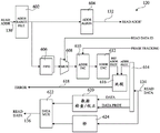
FIG. 4 schematically illustrates the write address protection circuitry 118 of FIG. 1 in greater detail according to an example embodiment.
The input address bus (WRITE ADDR)122 is coupled to, for example, an address range filter (ADDR RANGE FILT)402, which allows, for example, address protection/validation to be provided to specific address ranges in memory-only devices. For example, a memory device may be subdivided into a first portion for which address protection/verification is to be provided and another portion for which address protection/verification is not to be provided.
The output of the circuit 402 is coupled to an address alignment circuit (ADDR ALIGN)404 that, for example, increases the write address range to allow address protection values and, optionally, data protection values to be inserted. As a simple example, the memory device may have an addressing range (in hexadecimal) from 0x00 to 0xFF, but the processing device 116 may only see an addressing range of half the total, e.g., a range of 0x00 to 0x 7F. Thus, each of these addresses is translated, for example, into two adjacent physical addresses in the memory device, with address 0x7F becoming 0xFE, address 0x01 becoming 0x02, address 0x02 becoming 0x04, and so on. These translations correspond to a simple left shift of one bit of each address. The modified write address WRITE ADDR' is provided on the output address bus 124.
The write address from the address filter 402 is also provided, for example, to a first-in-first-out (FIFO) buffer 406, which stores, for example, one or more addresses, and provides them, upon request, to an address incrementer (ADDR INC)408, which is used, for example, to generate an address to be accessed during a write operation based on the write address. The address incrementer 408 is, for example, adapted to increase the address by a width corresponding to the width of the write data bus 122. For example, if the write data bus 122 is 8 bytes wide and the least significant bit of the address specifies one byte, the address incrementer 408 is adapted, for example, to increment the address by an increment of 8 with each new block of write data on the write data bus 126.
The output of the address incrementer 408 is provided to an address encoder (ADDR ENC)410, which generates a Y-bit address protection value, e.g., based on the address value, and provides the Y-bit value to a cascade circuit 412. The address encoder 410 generates an address protection value based on, for example, an address of a corresponding N-bit data value. In the case where the data bus width M is equal to N, the address encoder 410 will simply generate an address protection value based on the address provided by the address incrementer 408. However, if M is equal to PxN, where P is an integer of 2 or more, the address encoder generates, for example, P different protection values, one for each block of N bits across the width of the data bus.
For example, where the data bus width is equal to 2N, the address encoder 408 generates a first address protection value for writing a first N bits of data, e.g., based on the address provided by the address incrementer 408, and then generates a second address protection value for writing a second N bits of data, based on the address provided by the address incrementer 408 incremented by 1.
The cascade circuit 412 also receives N bits of system data provided on the input write data bus 126. In the example of fig. 4, the bus 126 is also coupled to a DATA encoder circuit 414(DATA ENC) that encodes DATA, for example, to generate a DATA protection value of X bits, which is also provided to the cascade circuit 412.
In some embodiments, the address protection/verification circuitry 112 implements slicing such that different portions of the data bus width are processed in parallel. In such a case, each of the address encoder 410, the connection circuit 412, and the data encoder 414 is instantiated, for example, multiple times based on the number of slices. The elements 410, 412, 414 of each slice, for example, process a respective block of an N-bit data bus. Each of the instances of the address encoder 410, for example, operates on a respective fixed offset of addresses representing the location of N bits of data within the width of the data bus. Furthermore, in some embodiments, the granularity of read or write accesses is lower than the width of the data bus, and corresponds to bytes, for example, while the data bus has a width equal to a number of bytes. Thus, a read or write operation may point to a particular starting byte across the width of the data bus.
As a specific example, in one embodiment, M is equal to 2N, and N is equal to 8. There are, for example, 2 slices, which means that each of the address encoder 410, the concatenation circuit 412 and the data encoder 414 is instantiated twice. In such an embodiment, the following table provides an example of consecutive addresses provided by the address incrementer (ADDR INC)408 and encoded by a first one of the address encoders (addrrenc #1)410 and by a second one of the address encoders (ADDR ENC # 2):


fig. 5 is a flowchart illustrating operations in a method of verifying an address according to an exemplary embodiment.
In operation 501, a read address is received.
In a subsequent operation 502, the read address is processed to generate a Y-bit reference address protection value. The same encoding algorithm as applied in operation 302 of fig. 3 is applied in operation 502.
In a subsequent operation 503, the address range of the read access is increased to cover a block of at least N + Y bits. This involves the same modification as described with respect to operation 303 of fig. 3, except that it is applied to a read address, rather than a write address.
In a subsequent operation 504, a memory access is performed and N + Y bits are read from the memory device.
In a subsequent operation 505, the Y-bit address protection value read from the memory device is compared to a reference address protection value. If there is a match, it is assumed, for example, that no address corruption has occurred. However, if there is a mismatch, an alarm is generated, for example, and the read data may be discarded.
FIG. 6 illustrates address verification circuitry 120 of FIG. 1 in greater detail in accordance with an example embodiment.
As shown, the READ address (READ ADDR) of address path 130 is provided, for example, to an address range filter (ADDR RANGE FILT)602, which is, for example, similar to circuit 402 of FIG. 4.
The output of the address range filter 602 is provided, for example, to an address alignment circuit (ADDR ALIGN)604, which also operates in the same manner as the circuit 404 of FIG. 4, for example, by increasing the address range of the read address to cover both system data and corresponding address protection values. The circuit 604 provides a READ address READ ADDR' on the output address bus 132.
The output of the address range filter 602 is also provided, for example, to a FIFO 606, which is coupled to an address incrementer (ADDR INC)610 via a Multiplexer (MUX) 608. The output of the address incrementer 610 is coupled to an address encoder (ADDR ENC)612, which generates a reference address protection value (REF ADDR PROT) based on the read address. The address incrementer 610 and address encoder 612 operate, for example, in a similar manner to the address incrementer 408 and address encoder 410.
The multiplexer 608 is controlled, for example, by a signal READ DATA ID from the memory device 104, which indicates, for example, which read data is provided on the bus 134, so that the multiplexer 608 selects the corresponding read address from the FIFO 606. Address incrementer 610, for example, receives one or more phase tracking signals (PAHSE TRACK) and is used to ensure that the address generated by incrementer 610 corresponds to the read data present on bus 134. In the case where the interface with the memory device is an AXI connection, the one or more phase tracking signals include, for example, signals RVALID, RREADY, and RLAST, which are known to those skilled in the art.
In some embodiments, a DATA checking/correction circuit (DATA CHECKING/CORRECTING)620 is also provided that receives from the splitter circuit 614 the system DATA (DATA) extracted from the read DATA by the splitter 614 and the X-bit DATA protection value (DATA PROT) extracted from the read DATA by the splitter 614. The output of circuit 620 is coupled to, for example, a DATA multiplexer (DATA MUX)622 that provides read DATA on output bus 136.
In some embodiments, the slices may be implemented in the address verification circuitry 120 in a similar manner as described above with respect to fig. 4. In the embodiment of FIG. 6, elements 612, 614, 616, and 620 are, for example, replicated such that each instantiation of these elements processes a respective block of N bits.
An advantage of the embodiments described herein is that address protection is provided in a relatively simple manner while maintaining a standard interface with memory devices. In fact, for example, only the width of the data bus used for increasing the memory device is modified, for example by multiplying its width.
Having thus described at least one illustrative embodiment, various alterations, modifications, and improvements will readily occur to those skilled in the art.
In particular, although an example has been described in which the sum of the X bits of the data protection value and the Y bits of the address protection value is equal to the number of bits N of the system data, many other formats are possible. For example, X + Y can be made equal to N/2 or N/4.
Claims (15)
1. A circuit for protecting memory address data, the circuit adapted to:
receiving write data to be written to the memory device (104) on an input data bus (126) and a corresponding write address on an address bus (122);
generating an address protection value based on the write address;
generating modified write data (WRITE DATA') on an output data bus (128), the modified write data including the write data and the address protection value, wherein a width of the output data bus (128) is greater than a width of the input data bus; and
generating a modified write address (WRITE ADDR') to the memory device on an output address bus (124) based on the write address.
2. The circuit of claim 1, wherein the circuit is further adapted to generate a data protection value based on the write data, the modified write data further comprising the data protection value.
3. The circuit of claim 1, further comprising an address generation circuit (404), the address generation circuit (404) adapted to generate the modified write address (WRITE ADDR') to the memory device on the output address bus (124).
4. A circuit according to claim 3, wherein the address generation circuit (404) is adapted to generate the modified write address (WRITE ADDR') by shifting the write address one bit to the left.
5. The circuit of claim 1, wherein the number of bits N of write data is less than a width M of an input data bus (126), and the address protection value is generated based on a sub-address corresponding to a location of the N bits of write data within the width of the address bus.
6. A circuit according to claim 1, wherein the width M of the input data bus (126) is equal to P times the number of bits N of the write data, the circuit comprising P address encoders, each address encoder being adapted to generate the address protection value based on a corresponding one of the sub-addresses.
7. The circuit of claim 1, wherein the protection data generation circuit (410) is adapted to generate the address protection value by encoding the write address to generate a Y-bit value, wherein Y is smaller than a number of bits of the write address.
8. The circuit of claim 1, further comprising an address range filter circuit (402), the address range filter circuit (402) adapted to determine whether the write address is in an address range to be protected, wherein the address protection value is generated only when an address is in the address range to be protected.
9. The circuit of claim 8, further comprising a bypass path for providing the write data directly to the write data output bus (128) if the write address is not in the address range to be protected, the bypass path comprising a bridge circuit (418), the bridge circuit (418) being adapted to convert N bits of write data into at least N + Y bits of write data.
10. A circuit for verifying memory address data, the circuit adapted to:
receiving a read address on an address bus (130);
generating a modified read address to a memory device (104) on an output address bus (132) based on the read address;
generating a reference address protection value (REF ADDR PROT) based on the read address;
receiving read data from the memory device (104) and an address protection value read from the memory device on a read data input bus (134); and
verifying the memory address data by comparing the address protection value read from the memory device to the reference address protection value.
11. The circuit of claim 10, wherein the number of bits N of read data is less than a width M of a read data portion of the read data input bus (134), and the reference address protection value is generated based on a sub-address corresponding to a location of N bits of read data within the width of the read data portion of the read data input bus (134).
12. A circuit according to claim 11, wherein the width M of the read data portion of the read data input bus (134) is equal to P times the number of bits N of the read data, the circuit comprising P address encoders, each address encoder being adapted to generate the address protection value based on a respective one of the sub-addresses.
13. An address protection/verification circuit (112) comprising a circuit (112) according to claim 1 and a circuit according to claim 10.
14. A method of protecting memory address data, comprising:
receiving write data to be written to the memory device (104) on an input data bus (126) and a corresponding write address on an address bus (122);
generating an address protection value based on the write address;
generating modified write data (WRITE DATA') on an output data bus (128), the modified write data including the write data and the address protection value, wherein a width of the output data bus (128) is greater than a width of the input data bus; and
generating a modified write address (WRITE ADDR') to the memory device on an output address bus (124) based on the write address.
15. A method of verifying memory address data, comprising:
receiving a read address on an address bus (130);
generating a modified read address to a memory device (104) on an output address bus (132) based on the read address;
generating a reference address protection value (REF ADDR PROT) based on the read address;
receiving read data from the memory device (104) and an address protection value read from the memory device on a read data input bus (134); and
verifying the memory address data by comparing the address protection value read from the memory device to the reference address protection value.
Applications Claiming Priority (2)
| Application Number | Priority Date | Filing Date | Title |
|---|---|---|---|
| FR1556621A FR3038752B1 (en) | 2015-07-10 | 2015-07-10 | METHOD AND CIRCUIT FOR PROTECTING AND VERIFYING ADDRESS DATA |
| FR1556621 | 2015-07-10 |
Publications (2)
| Publication Number | Publication Date |
|---|---|
| CN106340319A CN106340319A (en) | 2017-01-18 |
| CN106340319B true CN106340319B (en) | 2020-05-12 |
Family
ID=54848669
Family Applications (2)
| Application Number | Title | Priority Date | Filing Date |
|---|---|---|---|
| CN201610108842.8A Active CN106340319B (en) | 2015-07-10 | 2016-02-26 | Method and circuit for protecting and verifying address data |
| CN201620148491.9U Withdrawn - After Issue CN205692570U (en) | 2015-07-10 | 2016-02-26 | For protecting the circuit with verifying memory address date and address protection/checking circuit |
Family Applications After (1)
| Application Number | Title | Priority Date | Filing Date |
|---|---|---|---|
| CN201620148491.9U Withdrawn - After Issue CN205692570U (en) | 2015-07-10 | 2016-02-26 | For protecting the circuit with verifying memory address date and address protection/checking circuit |
Country Status (3)
| Country | Link |
|---|---|
| US (1) | US10248580B2 (en) |
| CN (2) | CN106340319B (en) |
| FR (1) | FR3038752B1 (en) |
Families Citing this family (8)
| Publication number | Priority date | Publication date | Assignee | Title |
|---|---|---|---|---|
| FR3038752B1 (en) * | 2015-07-10 | 2018-07-27 | Stmicroelectronics (Rousset) Sas | METHOD AND CIRCUIT FOR PROTECTING AND VERIFYING ADDRESS DATA |
| US10489241B2 (en) * | 2015-12-30 | 2019-11-26 | Arteris, Inc. | Control and address redundancy in storage buffer |
| CN108733311B (en) * | 2017-04-17 | 2021-09-10 | 伊姆西Ip控股有限责任公司 | Method and apparatus for managing storage system |
| FR3077893B1 (en) * | 2018-02-14 | 2020-09-11 | St Microelectronics Rousset | MEMORY ACCESS CONTROL SYSTEM |
| US10824560B2 (en) * | 2019-02-18 | 2020-11-03 | Nxp B.V. | Using a memory safety violation indicator to detect accesses to an out-of-bounds or unallocated memory area |
| US11789647B2 (en) * | 2019-12-20 | 2023-10-17 | Micron Technology, Inc. | Address verification for a memory device |
| CN113312294A (en) * | 2020-02-27 | 2021-08-27 | 瑞昱半导体股份有限公司 | Electronic device and communication method |
| CN112948167B (en) * | 2021-03-31 | 2022-10-18 | 地平线征程(杭州)人工智能科技有限公司 | Protection circuit, method, device and computer readable storage medium for data path |
Citations (4)
| Publication number | Priority date | Publication date | Assignee | Title |
|---|---|---|---|---|
| US5787481A (en) * | 1994-03-24 | 1998-07-28 | Texas Instruments Incorporated | System for managing write and/or read access priorities between central processor and memory operationally connected |
| CN1825296A (en) * | 2005-03-25 | 2006-08-30 | 威盛电子股份有限公司 | Interface circuit, system, and method for interfacing between buses of different widths |
| EP1873649A1 (en) * | 2006-06-28 | 2008-01-02 | Hitachi, Ltd. | Storage system and data protection method therefor |
| CN205692570U (en) * | 2015-07-10 | 2016-11-16 | 意法半导体(鲁塞)公司 | For protecting the circuit with verifying memory address date and address protection/checking circuit |
Family Cites Families (3)
| Publication number | Priority date | Publication date | Assignee | Title |
|---|---|---|---|---|
| JPH10320913A (en) * | 1997-05-23 | 1998-12-04 | Sony Corp | Apparatuses and method for recording data, for reproducing data, for recording reproducing data, and transmission medium |
| US7433980B1 (en) * | 2005-04-21 | 2008-10-07 | Xilinx, Inc. | Memory of and circuit for rearranging the order of data in a memory having asymmetric input and output ports |
| US8402349B2 (en) * | 2010-12-06 | 2013-03-19 | Apple Inc. | Two dimensional data randomization for a memory |
-
2015
- 2015-07-10 FR FR1556621A patent/FR3038752B1/en not_active Expired - Fee Related
-
2016
- 2016-02-26 CN CN201610108842.8A patent/CN106340319B/en active Active
- 2016-02-26 CN CN201620148491.9U patent/CN205692570U/en not_active Withdrawn - After Issue
- 2016-02-29 US US15/055,896 patent/US10248580B2/en active Active
Patent Citations (4)
| Publication number | Priority date | Publication date | Assignee | Title |
|---|---|---|---|---|
| US5787481A (en) * | 1994-03-24 | 1998-07-28 | Texas Instruments Incorporated | System for managing write and/or read access priorities between central processor and memory operationally connected |
| CN1825296A (en) * | 2005-03-25 | 2006-08-30 | 威盛电子股份有限公司 | Interface circuit, system, and method for interfacing between buses of different widths |
| EP1873649A1 (en) * | 2006-06-28 | 2008-01-02 | Hitachi, Ltd. | Storage system and data protection method therefor |
| CN205692570U (en) * | 2015-07-10 | 2016-11-16 | 意法半导体(鲁塞)公司 | For protecting the circuit with verifying memory address date and address protection/checking circuit |
Also Published As
| Publication number | Publication date |
|---|---|
| CN106340319A (en) | 2017-01-18 |
| US10248580B2 (en) | 2019-04-02 |
| FR3038752B1 (en) | 2018-07-27 |
| CN205692570U (en) | 2016-11-16 |
| FR3038752A1 (en) | 2017-01-13 |
| US20170010980A1 (en) | 2017-01-12 |
Similar Documents
| Publication | Publication Date | Title |
|---|---|---|
| CN106340319B (en) | Method and circuit for protecting and verifying address data | |
| US7149945B2 (en) | Systems and methods for providing error correction code testing functionality | |
| WO2008115400A1 (en) | Ecc implementation in non-ecc components | |
| US5331645A (en) | Expandable digital error detection and correction device | |
| US9665423B2 (en) | End-to-end error detection and correction | |
| JP2006293982A (en) | Flash memory device with reduced access time | |
| US6105155A (en) | Method and apparatus for performing on-chip function checks and locating detected anomalies within a nested time interval using CRCs or the like | |
| US20050081129A1 (en) | Bus device that concurrently synchronizes source synchronous data while performing error detection and correction | |
| US20220327020A1 (en) | Error rate reduction in a non-volatile memory (nvm), including magneto-resistive random access memories (mrams) | |
| WO1990002374A1 (en) | Failure detection for partial write operations for memories | |
| US20050289409A1 (en) | Parallel data bus | |
| US20200349001A1 (en) | System and Method for Transparent Register Data Error Detection and Correction via a Communication Bus | |
| US7321996B1 (en) | Digital data error insertion methods and apparatus | |
| CN108304277B (en) | Error correction method and device in flash memory | |
| JP6673021B2 (en) | Memory and information processing device | |
| TW201918925A (en) | Data accessing device and method | |
| US10250279B2 (en) | Circuits and methods for writing and reading data | |
| US9983926B2 (en) | Apparatus, system and method for protecting data | |
| US11797306B2 (en) | Circuit for verifying the content of registers | |
| US5774482A (en) | Apparatus and method for processing errors associated with data transfers in a computer | |
| US20210318873A1 (en) | Circuit for Verifying the Content of Registers | |
| CN210984286U (en) | Error correction code memory and electronic circuit | |
| US20240053904A1 (en) | Efficient security metadata encoding in error correcting code (ecc) memory without dedicated ecc bits | |
| US20230359523A1 (en) | Memory integrity check | |
| US6701472B2 (en) | Methods for tracing faults in memory components |
Legal Events
| Date | Code | Title | Description |
|---|---|---|---|
| C06 | Publication | ||
| PB01 | Publication | ||
| C10 | Entry into substantive examination | ||
| SE01 | Entry into force of request for substantive examination | ||
| GR01 | Patent grant | ||
| GR01 | Patent grant |