CN1054931C - Shared bus non-sequential data ordering method and apparatus - Google Patents
Shared bus non-sequential data ordering method and apparatus Download PDFInfo
- Publication number
- CN1054931C CN1054931C CN95102491A CN95102491A CN1054931C CN 1054931 C CN1054931 C CN 1054931C CN 95102491 A CN95102491 A CN 95102491A CN 95102491 A CN95102491 A CN 95102491A CN 1054931 C CN1054931 C CN 1054931C
- Authority
- CN
- China
- Prior art keywords
- data
- transmission
- bus
- value
- chip
- Prior art date
- Legal status (The legal status is an assumption and is not a legal conclusion. Google has not performed a legal analysis and makes no representation as to the accuracy of the status listed.)
- Expired - Fee Related
Links
Images

Classifications
-
- G—PHYSICS
- G06—COMPUTING; CALCULATING OR COUNTING
- G06F—ELECTRIC DIGITAL DATA PROCESSING
- G06F13/00—Interconnection of, or transfer of information or other signals between, memories, input/output devices or central processing units
- G06F13/14—Handling requests for interconnection or transfer
-
- G—PHYSICS
- G06—COMPUTING; CALCULATING OR COUNTING
- G06F—ELECTRIC DIGITAL DATA PROCESSING
- G06F13/00—Interconnection of, or transfer of information or other signals between, memories, input/output devices or central processing units
- G06F13/38—Information transfer, e.g. on bus
- G06F13/40—Bus structure
- G06F13/4004—Coupling between buses
- G06F13/4009—Coupling between buses with data restructuring
- G06F13/4018—Coupling between buses with data restructuring with data-width conversion
Landscapes
- Engineering & Computer Science (AREA)
- Theoretical Computer Science (AREA)
- General Engineering & Computer Science (AREA)
- Physics & Mathematics (AREA)
- General Physics & Mathematics (AREA)
- Computer Hardware Design (AREA)
- Memory System Of A Hierarchy Structure (AREA)
- Bus Control (AREA)
- Information Transfer Systems (AREA)
- Information Retrieval, Db Structures And Fs Structures Therefor (AREA)
- Small-Scale Networks (AREA)
Abstract
A shared bus non-sequential data ordering method and apparatus are provided. A maximum bus width value and a minimum transfer value are identified, responsive to which a minimum number of sub-transfers is identified. A bus unit having a maximum number of chips to receive and/or send data receives data in a predefined order during multiple sub-transfers.
Description
The present invention relates generally to data handling system, more specifically, relate to a kind of shared bus non-sequential data (Shared bus non-Sequential dataordering) sort method and the device of data handling system.
Data processing or computer system comprise a common data path that is called bus usually.This bus connects such as bus units such as processor, storer and memory devices.Data are transmitted between bus unit via bus.The transmission speed of data on bus is a pith of performance of computer systems.
The demand that improves data rate on the bus is to be motive with number that improves the instruction that processor can carry out and the speed that processor can execute instruction.Along with the arrival that can be widely on chip piece surpasses 1,000,000 transistorized integrated technologies, and still continue development at present, currently may make ultra-large and VLIW (very large instruction word) processor.These processors are carried out the instruction of one or more usually in one-period, this has improved the transmission requirements to the mass data that commutes storer or memory device.Except the integration density that has improved processor, processor speed improves sooner than memory access time, even surpasses the journey time of signal on bus.This velocity mismatch has also increased the demand to transferring large number of data.
In order to satisfy this ever-increasing demand to mass data, the speed of bus needs to improve.Article one, the shared bus speed that can transmit data partly depends on physical length, the load on the bus and the minimum transfer amount (being also referred to as highway width or bus scale) of bus.The physical length of bus only is the length of the line between the bus unit.The physical length of bus is big more, and bus is slow more.Load is the impedance on the line of the seen bus of driver.Load is big more, and bus is slow more.The number of the bus unit on this bus and the load that each bus unit provides are depended in load on the bus.The minimum transfer amount is a data volume of once transmitting bus.The minimum transfer amount is big more, and data rate is fast more.In order to satisfy the requirement of modern processors, the desirable minimum transfer scale on processor or the desired bus of its Cache from four or Eight characters joint bring up to 16 or 32 bytes and more than.
Unfortunately limit owing to the minimum transfer scale is subjected to the physics restriction, the scale that only improves minimum transfer in order to improve bus transfer speed is not forever possible.These physics restrictions comprise: the number of the I/O lead-in wire on chip, chip module and the card connector; The wiring restriction of chip, card and multi-chip module: and the cost of width bus.Along with integrated circuit becomes more intensive and the data throughout ability that increases day by day is provided, the ability of the required data throughout of providing of module and card is being provided for they.Even exist the technology of the I/O ability of using chip, it also is unacceptable on cost, has to adopt older, lower-cost encapsulation technology for market competition.
Thereby because the restriction of physics and cost, the computer system of a complexity has the bus of many different scales.For example, the cached data bus may be wideer than main memory data bus.When two buses of different scales linked together, the transmission scale of a bus must convert the transmission scale of another bus to.In order to accomplish this point,, need two or more son transmission form the minimum transfer scale when when bigger transmission scale is transformed into less transmission scale.Existing conversion method adopts alphabetic data ordering (Sequentialdata ordering), wherein each byte and its adjacent byte rank order on data bus.For example, when bigger transmission scale is transformed into less transmission scale, the first of the whole width of transmission earlier, second portion, third part or the like then are up to finishing conversion.United States Patent (USP) 5,243,701st adopts the alphabetic data ordering to have the example of a kind of memory sub-system of the ability of working on one eight or 16-bit bus.
A problem of these existing conversion methods is that when a plurality of chips were connected with bus, they can increase load and reduce performance.Owing to need wide minimum transfer to improve bus speed, have a plurality of chips and bus interface usually.In these chips each receives the data of part transmission, and in the chip load that has on the bus more than.The example that is connected the multicore sheet on the data bus can be 4 DRAM (dynamic RAM) controller chips, and each controls the DRAM of 4 bytes so that the minimum transfer scale of 16 bytes to be provided.Another example is 4 director cache chips, and each chip comprises the Cache of 4 byte datas, and they also provide the minimum transfer scale of 16 bytes.
Progress in integrated circuit and the processor design proposes one group of new problem to the deviser of shared bus.Transmission of the minimum data of the desired non-constant width of processor that these are up-to-date and their shortening cycle length promote the shared bus deviser and in than the shorter in the past time, transmit more data.When shared bus width during less than desired minimum transfer, the data of being asked must transmission in the transmission of the son more than twice or twice.In order to keep bus to operate in the cycle length of processor, the deviser also must reduce the load on the bus.Because the demand to wide minimum transfer has the polylith chip to be connected with bus usually.If the deviser adopts current technology to convert the transmission scale that requires of minimum to the actual bus width, will on bus, produce very large load, thereby reduce its speed.Below shared bus non-sequential data ordering method and device in the remarkable improvement that provides aspect the demand of coherent system and the restriction prior art.
A fundamental purpose of the present invention is for providing a kind of shared bus non-sequential data ordering method and device, and it overcomes many shortcomings of prior art layout by the performance that reduces bus load and improvement bus.
Purpose of the present invention and advantage reach with a kind of shared bus non-sequential data ordering method and device.At first, determine a maximum bus width value and a minimum transfer value.The second, determine that according to the maximum bus width value of determining and minimum transfer value boy transmits number.The 3rd, determine to have a bus unit of the chip of the maximum number that is used to receive and send data.At last, in the transmission of each data, to or from the predetermined word of the correspondence of each chip transmission of the bus unit determined with the chip of the maximum number on the bus.
From following in the detailed description that is illustrated in the embodiments of the invention the accompanying drawing, can understand well the present invention with and above-mentioned and other purpose and advantage, wherein:
Fig. 1 implements the block scheme of computing machine of the present invention or data handling system for expression;
Fig. 2 is the block scheme of illustration a kind of numerical nomenclature agreement of the present invention;
Fig. 3 is the figure according to a data ordering example of sort method of the present invention and device;
Fig. 3 A is the process flow diagram of illustration according to the sequential steps of data reordering method of the present invention;
Fig. 4 is that illustration is to the byte number of one 16 byte main memory bus and the figure of ordering;
Fig. 5 is that illustration is to the byte number of one 32 byte main memory bus and the figure of ordering; And
Fig. 6 is the block scheme that a kind of alphabetic data ordered bus of illustration is arranged.
Referring to the Fig. 1 in the accompanying drawing, wherein show and implement a computing machine of the present invention or data handling system, represent with reference number 10.Storer that computer system 10 comprises a processor 12, use with a main memory controller unit (MSCU) 16 or primary memory 14, this MSCU comprises a plurality of Caches/Memory Controller chip CHIP 0, CHIP 1, CHIP 2 and CHIP 3, and has a shared main storage bidirectional bus with the employing non-sequential data ordering of reference number 18 indications.
According to feature of the present invention, this shared bus non-sequential data ordering method is compared with the bus arrangement of ordering sequentially shown in Fig. 6 with device, provide the bus load that reduces with multicore film source and destination, the I/O counting of improved bus performance and minimizing.The I/O counting that reduces is from the interface wide to the single word of each chip.Data sort with non-sequential grammar, make the bus unit of reception with maximum number or the chip that sends data sequentially transfer data to each chip in the son transmission.
Adopt the sort method of invention shown in Figure 1, each bus unit of the each several part of data bus 18 has only a load.Bus unit among Fig. 1 is primary memory 14 and MSCU16.The transmission of first data comprises word 0,2,4,6.When first second son was transmitted, each chip CHIP 0, CHIP 1, CHIP 2 and CHIP 3 obtained a word, and promptly the even number word 0,2,4,6.Data transmission for the second time comprises odd number word 1,3,5,7.When second second son was transmitted, each chip CHIP 0, CHIP 1, CHIP 2 and CHIP 3 obtained a word, and promptly the odd number word 1,3,5,7.Adopt this method, each chip only needs the interface that individual character is wide.The wide interface of individual character is more cheap, obtains less encapsulation, and stays more zone for other function use on chip.
A kind of numerical nomenclature of Fig. 2 illustration agreement, Fig. 3 then illustration according to data of non-sequential data ordering method of the present invention and the device example that sorts.Available caches is determined minimum data transmission width X to the interface of processor.For having X/2 available I/O lead-in wire, represent a less bus Y with the X/2 byte.Four Caches/Memory Controller chip CHIP 0, CHIP 1, CHIP 2 and CHIP 3 are arranged in Fig. 1, each chip obtains the data of X/4 byte, because data bus Y is desired minimum transfer half, finishing once, transmission needs two second sons transmission (ST).X byte be defined as comprise that n word, one of them word are exactly the son transmission scale of each chip.Shown in example in, n=X/8.For each second son transmission, each Cache/Memory Controller chip CHIP 0, CHIP 1, CHIP 2, CHIP 3 supply with 1/8th of total transmission.This is because each chip needs X/4 byte, but has to half with each son transmission.
For example, as shown in fig. 1, each receiving element that receives among the MSCU16 in logic is CHIP 0, CHIP 1, CHIP 2 and CHIP 3, with the repeatedly transmission reception data of non-rank order.For example, suppose that desired data transmission width is an X byte, comprise and be numbered 8 words of 0,1,2,3,4,5,6,7.X byte is that son is transmitted in and sends on the bus or transmission at twice, is word 1,3,5,7 then as word 0,2,4,6.
As a result, each receiving element CHIP 0, CHIP 1, CHIP 2, CHIP 3 are with the sequential order reception data of standard.Receiving element CHIP 0 receives word 0,1.Receiving element CHIP 1 receives word 2,3.Receiving element CHIP 2 receives word 4,5.Receiving element CHIP 3 receives word 6,7.
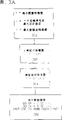
Referring to Fig. 3 A, wherein show the process flow diagram of determining the sequential steps of sub-transmission scale and data sorting according to data reordering method of the present invention.Follow is the non-rank order method of representing with mathematical formulae in the back.At first in frame 300, make X equal the byte number in the minimum data transmission one time; Make i equal maximum chip-count on the bus unit, and make Y equal to be subjected to the maximum-norm of the data bus of I/O restriction.
Then in frame 302, determine required son transmission number, make j equal to carry out the required son transmission number of minimum transfer one time, j is defined as:
J=X/Y, wherein j is an integer.If Y is not 2 power, then rounding up draws integer j.
Then in frame 304, determine a round values n who equals a byte number in the word, n is defined as follows:
N=X/ (i*j), wherein n is an integer, is assumed to one 2 power.
Then in frame 306, carry out a kind of data sorting algorithm as giving a definition:
Do ST=0 to j-1;---be each son transmission
Do CN=0 to i-1;---be each chip
Chip (CN)<=word{ (CN*j)+ST}; End---this word is to this chip end;
Though the do in the frame 306 circulates in each second son transmission a specific letter lock is fixed in the specific chip, the data sorting that should be understood that other also is possible and may is desirable.Required I/O lead-in wire is reduced and makes chip I/O (I/O) count with time bus cycles between the bus unit becomes minimum.
Following table 1 is listed the data sorting of the example shown in Fig. 1, wherein j=2 and i=4.
Table 1
CN ST
(chip number) (transmission)
O 1
CHIP 0 word 01
CHIP 1 word 23
CHIP 2 words 45
CHIP 3 words 67
Fig. 4 and 5 provides the figure for the byte number of 16 byte main memory bus of one time 128 byte cache-lines transmission and 32 byte main memory bus.For 16 byte buses, Y=X/2 and for 32 byte buses, Y=X.
Referring to Fig. 6, wherein show the example of the data bus of a rank order.Notice that the each several part of this data bus has two loads on each Cache/Memory Controller bus unit.The first second son transmission package is drawn together to the byte 0-3 of chip 0 with chip 1.Chip 0 obtains 2 words 0,1 and word 2,3 respectively with chip 1.The second son transmission comprises word 4-7, and wherein word 4,5 and word were clipped to chip 2 and chip 3 in 6,7 minutes.Data bus has two loads for each bus unit with 4 chip blocks.This can reduce bus performance.In addition, each chip needs one the two wide interface of word.If this system has a plurality of unit of band four-core sheet interface, such as multiprocessor and memory card, additional load is tangible.
Though the present invention describes with reference to the details of illustrated embodiment, these details are not intended to limit defined invention scope in the appending claims.
Claims (8)
1. a shared bus non-sequential data ordering method that is used in the data handling system comprises the following steps:
Determine a maximum bus width value;
Determine a minimum transfer value;
According to described definite minimum transfer value and described maximum bus width value, determine a sub-transmission value;
Determine that one has the reception of maximum number and the bus unit of the chip that sends data;
Utilize described definite sub-transmission value,, predetermined word is transferred to described chip for each data transmission.
2. a kind of shared bus non-sequential data ordering method described in the claim 1 is wherein saidly determined a minimum transfer value; Determine a maximum bus width value; And determine that according to described definite minimum transfer value and described maximum bus width value the step of a sub-transmission value comprises the steps:
Definite described minimum transfer value of representing with X;
Definite described maximum bus width value of representing with Y;
Definite described sub-transmission value of representing with j=X/Y, wherein X, Y and j are integer.
3. shared bus non-sequential data collator that is used in the data handling system comprises:
Be used for determining the device of a minimum transfer value;
Be used for determining the device of a minimum highway width value;
Be used for determining the device of a sub-transmission value according to described definite minimum transfer value and described maximum bus width value, this device links to each other with above-mentioned two definite devices;
Be used to determine the device of a bus unit of the chip that has the reception of maximum number or send data; And
Be data transmission each time, be used for the reserved word of a correspondence is transferred to the device of each described bus unit chip, this device is used for determining that with described the device of sub-transmission value links to each other, and the reserved word of described correspondence is to utilize described definite sub-transmission value to determine.
4. a kind of shared bus non-sequential data collator described in the claim 3 is characterized in that described predetermined word comprises the n byte, and wherein n is defined as n=X/ (i
*J), and n be an integer.
5. a kind of shared bus non-sequential data collator described in the claim 4, it is characterized in that described sub-transmission value equals 2, and be used for the described device that reserved word with a correspondence is transferred to each described bus unit chip and be included in the device of first second son transmission transmission even number word and the device that in the transmission of second second son, transmits the odd number word.
6. one kind is used for the data reordering method that has the shared bidirectional bus transmitting data of a maximum bus width value and a minimum transfer value at one, comprises the steps:
Determine the minimal amount that son transmits according to described definite maximum bus width value and described minimum transfer value;
Determine a bus unit that has the reception of maximum number and send the chip of data; And
In the transmission of secondary data, transmit one group of predetermined word, each word is transferred to the chip piece of described bus unit.
7. a kind of data reordering method described in the claim 6, the minimal amount that it is characterized in that described data transmission value equals 2, and the described step that each word with one group of predetermined word in the transmission of described data is transferred to each described bus unit chip comprises the steps:
Transmission even data word in the data transmission first time; And
Transmission odd data word in the data transmission second time.
8. a kind of data reordering method described in the claim 6 is characterized in that the described one group of predetermined word that is transmitted has a kind of predetermined order in each data transmission.
Applications Claiming Priority (3)
| Application Number | Priority Date | Filing Date | Title |
|---|---|---|---|
| US22214794A | 1994-04-01 | 1994-04-01 | |
| US222147 | 1994-04-01 | ||
| US222,147 | 1994-04-01 |
Publications (2)
| Publication Number | Publication Date |
|---|---|
| CN1117617A CN1117617A (en) | 1996-02-28 |
| CN1054931C true CN1054931C (en) | 2000-07-26 |
Family
ID=22831053
Family Applications (1)
| Application Number | Title | Priority Date | Filing Date |
|---|---|---|---|
| CN95102491A Expired - Fee Related CN1054931C (en) | 1994-04-01 | 1995-03-16 | Shared bus non-sequential data ordering method and apparatus |
Country Status (9)
| Country | Link |
|---|---|
| US (1) | US5748919A (en) |
| EP (1) | EP0676702B1 (en) |
| JP (1) | JPH07281998A (en) |
| KR (1) | KR0175980B1 (en) |
| CN (1) | CN1054931C (en) |
| AT (1) | ATE166733T1 (en) |
| CA (1) | CA2142028A1 (en) |
| DE (1) | DE69502656D1 (en) |
| TW (1) | TW321744B (en) |
Families Citing this family (1)
| Publication number | Priority date | Publication date | Assignee | Title |
|---|---|---|---|---|
| US7765307B1 (en) * | 2006-02-28 | 2010-07-27 | Symantec Operating Corporation | Bulk network transmissions using multiple connections primed to optimize transfer parameters |
Citations (1)
| Publication number | Priority date | Publication date | Assignee | Title |
|---|---|---|---|---|
| US5280598A (en) * | 1990-07-26 | 1994-01-18 | Mitsubishi Denki Kabushiki Kaisha | Cache memory and bus width control circuit for selectively coupling peripheral devices |
Family Cites Families (16)
| Publication number | Priority date | Publication date | Assignee | Title |
|---|---|---|---|---|
| US4056845A (en) * | 1975-04-25 | 1977-11-01 | Data General Corporation | Memory access technique |
| US4514808A (en) * | 1978-04-28 | 1985-04-30 | Tokyo Shibaura Denki Kabushiki Kaisha | Data transfer system for a data processing system provided with direct memory access units |
| US4490819A (en) * | 1982-04-22 | 1984-12-25 | International Telephone And Telegraph Corporation | Rate converter |
| US4507731A (en) * | 1982-11-01 | 1985-03-26 | Raytheon Company | Bidirectional data byte aligner |
| US4837785A (en) * | 1983-06-14 | 1989-06-06 | Aptec Computer Systems, Inc. | Data transfer system and method of operation thereof |
| JPS61175845A (en) * | 1985-01-31 | 1986-08-07 | Toshiba Corp | Microprocessor system |
| JPS6226561A (en) * | 1985-07-26 | 1987-02-04 | Toshiba Corp | Personal computer |
| US5243701A (en) * | 1987-09-17 | 1993-09-07 | Mitsubishi Denki Kabushiki Kaisha | Method of and system for processing data having bit length variable with modes of operation |
| US4878166A (en) * | 1987-12-15 | 1989-10-31 | Advanced Micro Devices, Inc. | Direct memory access apparatus and methods for transferring data between buses having different performance characteristics |
| US5237676A (en) * | 1989-01-13 | 1993-08-17 | International Business Machines Corp. | High speed data transfer system which adjusts data transfer speed in response to indicated transfer speed capability of connected device |
| JPH03186928A (en) * | 1989-12-16 | 1991-08-14 | Mitsubishi Electric Corp | Data processor |
| US5287470A (en) * | 1989-12-28 | 1994-02-15 | Texas Instruments Incorporated | Apparatus and method for coupling a multi-lead output bus to interleaved memories, which are addressable in normal and block-write modes |
| JP2646854B2 (en) * | 1990-12-18 | 1997-08-27 | 三菱電機株式会社 | Microprocessor |
| US5255374A (en) * | 1992-01-02 | 1993-10-19 | International Business Machines Corporation | Bus interface logic for computer system having dual bus architecture |
| US5257391A (en) * | 1991-08-16 | 1993-10-26 | Ncr Corporation | Disk controller having host interface and bus switches for selecting buffer and drive busses respectively based on configuration control signals |
| US5293381A (en) * | 1992-03-27 | 1994-03-08 | Advanced Micro Devices | Byte tracking system and method |
-
1994
- 1994-08-25 TW TW083107806A patent/TW321744B/zh active
-
1995
- 1995-02-07 CA CA002142028A patent/CA2142028A1/en not_active Abandoned
- 1995-02-13 JP JP7024215A patent/JPH07281998A/en active Pending
- 1995-03-08 AT AT95480019T patent/ATE166733T1/en not_active IP Right Cessation
- 1995-03-08 EP EP95480019A patent/EP0676702B1/en not_active Expired - Lifetime
- 1995-03-08 DE DE69502656T patent/DE69502656D1/en not_active Expired - Lifetime
- 1995-03-16 CN CN95102491A patent/CN1054931C/en not_active Expired - Fee Related
- 1995-03-30 KR KR1019950006997A patent/KR0175980B1/en not_active IP Right Cessation
-
1996
- 1996-07-10 US US08/677,775 patent/US5748919A/en not_active Expired - Fee Related
Patent Citations (1)
| Publication number | Priority date | Publication date | Assignee | Title |
|---|---|---|---|---|
| US5280598A (en) * | 1990-07-26 | 1994-01-18 | Mitsubishi Denki Kabushiki Kaisha | Cache memory and bus width control circuit for selectively coupling peripheral devices |
Also Published As
| Publication number | Publication date |
|---|---|
| DE69502656D1 (en) | 1998-07-02 |
| ATE166733T1 (en) | 1998-06-15 |
| CA2142028A1 (en) | 1995-10-02 |
| EP0676702A1 (en) | 1995-10-11 |
| CN1117617A (en) | 1996-02-28 |
| EP0676702B1 (en) | 1998-05-27 |
| US5748919A (en) | 1998-05-05 |
| KR0175980B1 (en) | 1999-05-15 |
| KR950029955A (en) | 1995-11-24 |
| TW321744B (en) | 1997-12-01 |
| JPH07281998A (en) | 1995-10-27 |
Similar Documents
| Publication | Publication Date | Title |
|---|---|---|
| DE69530292T2 (en) | EFFICIENT ADDRESSING OF LARGE STORES | |
| CN1029048C (en) | Method and apparatus processing data in the distributed processing system | |
| CN1292342C (en) | System and device for addressing global variable by using multiple codes in integrated executable program of isomeric system structure | |
| US4994962A (en) | Variable length cache fill | |
| CN1517895A (en) | System and method for distributing multisource to multi-channel | |
| CN1286038C (en) | Dual-ring quene-based, non-interrupt PCI communication method | |
| FI74356C (en) | ANORDNING FOER STYRNING AV KOPPLING AV PROCESSORER TILL DATALEDNING. | |
| CN112256623B (en) | Heterogeneous system-based processing performance optimization method and device | |
| US4731737A (en) | High speed intelligent distributed control memory system | |
| CN1041566C (en) | Method and system for nonsequential instruction dispatch and execution in a superscalar processor system | |
| CN1054931C (en) | Shared bus non-sequential data ordering method and apparatus | |
| EP1227405A3 (en) | A method for providing a cache indexing scheme less susceptible to cache collisions | |
| US5668975A (en) | Method of requesting data by interlacing critical and non-critical data words of multiple data requests and apparatus therefor | |
| CN115982311A (en) | Chain table generation method and device, terminal equipment and storage medium | |
| CN100547569C (en) | Be used for transmitting the electronic data processing circuit of packing word and the method for deal with data via bus | |
| CN1105977C (en) | Multi-processor system provided with bus control module | |
| Chow | The analysis and design of some new sorting machines | |
| KR920004971A (en) | Microprocessors and Data Unit Processing Methods | |
| CN1046040C (en) | Direct access structure of memory matched with bus bits | |
| Sethi et al. | Heuristic methods for selection and ordering of part-orienting devices | |
| EP4325368A1 (en) | Systems and methods for inference system caching | |
| CN1043023A (en) | Microprocessor is directed to interrupt | |
| CN1197519A (en) | Processor with instruction cache | |
| CN117591509A (en) | Inference system and method for inference system | |
| CN1168729A (en) | System and method for processing of memory data and communication system comprising such system |
Legal Events
| Date | Code | Title | Description |
|---|---|---|---|
| C10 | Entry into substantive examination | ||
| SE01 | Entry into force of request for substantive examination | ||
| C06 | Publication | ||
| PB01 | Publication | ||
| C14 | Grant of patent or utility model | ||
| GR01 | Patent grant | ||
| C17 | Cessation of patent right | ||
| CF01 | Termination of patent right due to non-payment of annual fee |
Granted publication date: 20000726 |