CN105452998B - Method for multizone capacitive sensing, device and apparatus for carrying out the method - Google Patents
Method for multizone capacitive sensing, device and apparatus for carrying out the method Download PDFInfo
- Publication number
- CN105452998B CN105452998B CN201480027820.8A CN201480027820A CN105452998B CN 105452998 B CN105452998 B CN 105452998B CN 201480027820 A CN201480027820 A CN 201480027820A CN 105452998 B CN105452998 B CN 105452998B
- Authority
- CN
- China
- Prior art keywords
- excitation
- electrodes
- potential
- electrode
- region
- Prior art date
- Legal status (The legal status is an assumption and is not a legal conclusion. Google has not performed a legal analysis and makes no representation as to the accuracy of the status listed.)
- Expired - Fee Related
Links
- 238000000034 method Methods 0.000 title claims abstract description 27
- 230000005284 excitation Effects 0.000 claims abstract description 116
- 230000008878 coupling Effects 0.000 claims abstract description 33
- 238000010168 coupling process Methods 0.000 claims abstract description 33
- 238000005859 coupling reaction Methods 0.000 claims abstract description 33
- 238000005259 measurement Methods 0.000 claims description 69
- 238000001514 detection method Methods 0.000 claims description 43
- 238000007667 floating Methods 0.000 claims description 9
- 230000000737 periodic effect Effects 0.000 claims description 4
- 230000003595 spectral effect Effects 0.000 claims 1
- 230000003071 parasitic effect Effects 0.000 description 10
- 238000010586 diagram Methods 0.000 description 6
- 230000001681 protective effect Effects 0.000 description 4
- 238000002059 diagnostic imaging Methods 0.000 description 3
- 230000000694 effects Effects 0.000 description 3
- 230000007613 environmental effect Effects 0.000 description 3
- 230000035945 sensitivity Effects 0.000 description 3
- 238000009825 accumulation Methods 0.000 description 2
- 238000013459 approach Methods 0.000 description 2
- 239000003990 capacitor Substances 0.000 description 2
- 230000001419 dependent effect Effects 0.000 description 2
- 239000011159 matrix material Substances 0.000 description 2
- 238000000691 measurement method Methods 0.000 description 2
- 230000010287 polarization Effects 0.000 description 2
- 238000001228 spectrum Methods 0.000 description 2
- 230000001360 synchronised effect Effects 0.000 description 2
- 241000699670 Mus sp. Species 0.000 description 1
- 241001422033 Thestylus Species 0.000 description 1
- 102100029469 WD repeat and HMG-box DNA-binding protein 1 Human genes 0.000 description 1
- 101710097421 WD repeat and HMG-box DNA-binding protein 1 Proteins 0.000 description 1
- 230000002411 adverse Effects 0.000 description 1
- 230000003321 amplification Effects 0.000 description 1
- 238000004891 communication Methods 0.000 description 1
- 238000011161 development Methods 0.000 description 1
- 239000006185 dispersion Substances 0.000 description 1
- 238000005516 engineering process Methods 0.000 description 1
- 230000036039 immunity Effects 0.000 description 1
- 230000002452 interceptive effect Effects 0.000 description 1
- 238000002372 labelling Methods 0.000 description 1
- 238000012986 modification Methods 0.000 description 1
- 230000004048 modification Effects 0.000 description 1
- 238000003199 nucleic acid amplification method Methods 0.000 description 1
- 230000010363 phase shift Effects 0.000 description 1
- 230000002123 temporal effect Effects 0.000 description 1
- 238000012546 transfer Methods 0.000 description 1
- 230000017105 transposition Effects 0.000 description 1
Images


Classifications
-
- G—PHYSICS
- G06—COMPUTING; CALCULATING OR COUNTING
- G06F—ELECTRIC DIGITAL DATA PROCESSING
- G06F3/00—Input arrangements for transferring data to be processed into a form capable of being handled by the computer; Output arrangements for transferring data from processing unit to output unit, e.g. interface arrangements
- G06F3/01—Input arrangements or combined input and output arrangements for interaction between user and computer
- G06F3/03—Arrangements for converting the position or the displacement of a member into a coded form
- G06F3/041—Digitisers, e.g. for touch screens or touch pads, characterised by the transducing means
- G06F3/0416—Control or interface arrangements specially adapted for digitisers
- G06F3/0418—Control or interface arrangements specially adapted for digitisers for error correction or compensation, e.g. based on parallax, calibration or alignment
-
- G—PHYSICS
- G06—COMPUTING; CALCULATING OR COUNTING
- G06F—ELECTRIC DIGITAL DATA PROCESSING
- G06F3/00—Input arrangements for transferring data to be processed into a form capable of being handled by the computer; Output arrangements for transferring data from processing unit to output unit, e.g. interface arrangements
- G06F3/01—Input arrangements or combined input and output arrangements for interaction between user and computer
- G06F3/03—Arrangements for converting the position or the displacement of a member into a coded form
- G06F3/041—Digitisers, e.g. for touch screens or touch pads, characterised by the transducing means
- G06F3/044—Digitisers, e.g. for touch screens or touch pads, characterised by the transducing means by capacitive means
- G06F3/0445—Digitisers, e.g. for touch screens or touch pads, characterised by the transducing means by capacitive means using two or more layers of sensing electrodes, e.g. using two layers of electrodes separated by a dielectric layer
-
- G—PHYSICS
- G06—COMPUTING; CALCULATING OR COUNTING
- G06F—ELECTRIC DIGITAL DATA PROCESSING
- G06F2203/00—Indexing scheme relating to G06F3/00 - G06F3/048
- G06F2203/041—Indexing scheme relating to G06F3/041 - G06F3/045
- G06F2203/04101—2.5D-digitiser, i.e. digitiser detecting the X/Y position of the input means, finger or stylus, also when it does not touch, but is proximate to the digitiser's interaction surface and also measures the distance of the input means within a short range in the Z direction, possibly with a separate measurement setup
-
- G—PHYSICS
- G06—COMPUTING; CALCULATING OR COUNTING
- G06F—ELECTRIC DIGITAL DATA PROCESSING
- G06F2203/00—Indexing scheme relating to G06F3/00 - G06F3/048
- G06F2203/041—Indexing scheme relating to G06F3/041 - G06F3/045
- G06F2203/04104—Multi-touch detection in digitiser, i.e. details about the simultaneous detection of a plurality of touching locations, e.g. multiple fingers or pen and finger
Abstract
The invention relates to a method of capacitive sensing, implementing a plurality of electrodes (5, 7) capable of detecting a target object (1) in the vicinity thereof by capacitive coupling, and comprising the step of simultaneously polarizing at least a part of the electrodes (5, 7) with different excitation potentials, said excitation potentials being generated with respect to a reference potential such that the inner product of at least two of these excitation potentials over a predetermined period of time is zero or much smaller than the inner product of one and/or the other of these excitation potentials with itself over said predetermined period of time. The invention also relates to a device and an apparatus for implementing said method.
Description
Technical Field
The invention relates to a method and a device for capacitive detection of multiple regions. The field of the invention is more particularly, but not exclusively, that of capacitive detection systems and touch and contactless human-machine interfaces.
Background
Many communication and working devices use a touch or non-contact measurement interface as a human-machine interface for inputting commands. These interfaces can in particular have the form of a flat panel or a touch screen. They are used, for example, in mobile phones, smart phones, touch screen computers, tablets, personal computers, mice, touch screens, widescreen and the like.
These interfaces typically use capacitive technology. The measuring surface is equipped with capacitive electrodes connected to an electronic unit that allows the variation of the capacitance generated between the measuring electrodes and the object to be detected to carry out the command.
Transparent electrodes may be implemented that allow the interface to be superimposed on a display screen (e.g., of a smartphone).
Most of these interfaces are touch interfaces, i.e. they are able to detect contact of one or more target or command objects (e.g. a finger or a stylus) with the interface surface.
Gestures or touchless interfaces are being developed more and more that are capable of detecting command objects at large distances from the interface without contact with the surface.
The development of contactless interfaces requires the implementation of very high sensitivity capacitive measurement techniques and the provision of high immunity to environmental disturbances. In fact, the capacitance generated between the capacitive measuring electrode of the interface and the command object is inversely proportional to the distance between them.
Document FR2756048, for example roziere, discloses a capacitive measurement method allowing to measure the capacitance and the distance between a plurality of independent electrodes and a nearby object.
This technique allows to obtain measurements of the capacitance between the electrode and the object with high resolution and high sensitivity, allowing to detect for example fingers at distances of a few centimeters or even tens of centimeters. The detection can be performed in three-dimensional space and on a surface called a measurement surface.
In general, the command object can be considered to be at a reference potential, such as an exposed conductive portion or ground.
In most capacitive detection techniques, the electrodes are polarized at an excitation voltage. Thus, the capacitive coupling between these polarized electrodes and the object at the reference potential is measured.
In the case of a portable device, such as a smartphone or tablet, the circuit includes a reference potential or internal ground, which floats with respect to ground potential as it is supplied by a battery. However, this internal reference potential is set to ground potential or at least to the potential of the user's body by the influence of capacitive coupling with its environment (especially when it is held in the user's hand). Thus, when the other hand is close to the measuring electrode, the hand is "seen" as being substantially at the internal reference potential or at the ground potential of the device.
It would be advantageous to develop portable devices, such as smart phones or tablets, which comprise a sensing surface with measuring electrodes in a location other than the display screen. Such devices can be equipped with electrodes, for example on the side opposite the screen and/or on the side, to detect further information items related to their environment, the way they are held, etc.
A problem that arises in this case is that due to the floating nature of the mounted electronics relative to ground potential, if the measurement electrode, which is polarized at the excitation voltage, is in contact with, or strongly (capacitively) coupled to, for example, a flashlight of a user holding the device, the entire body of the user is "seen" by the electronics as being substantially at the excitation potential. In this case, the command object, e.g. his other hand, is also "seen" as being substantially at the excitation potential of the electrodes. Then the capacitive coupling is zero or very weak and no object is detected or only an object at a short distance is detected.
Capacitive detection techniques are also used to equip systems, such as robots or mobile medical imaging devices (scanners, etc.), to make them sensitive to their environment. The principle is the same: the capacitive coupling between the capacitive electrode polarized at the excitation voltage and an environmental object considered to be at a reference potential, ground or earth potential is measured.
When two objects equipped with capacitive electrodes are displaced with respect to each other, there is a risk that they may not detect each other, since no capacitive coupling is established between them if the measuring electrodes are at the same potential. In addition, the protection principle used in most capacitive detection systems is: the electrodes are protected from undesired environmental influences (parasitic capacitances) by arranging the sensing surfaces in close proximity at the same excitation potential.
One subject of the present invention is to propose a method and a device for capacitive detection which are able to overcome these drawbacks of the prior art.
Another subject of the invention is to propose a capacitive detection method and apparatus which allow equipping devices floating with respect to the exposed conductive part or with respect to ground with capacitive detection electrodes capable of detecting the approach of a target object, so that the measurement is not or only slightly affected by the strong electrical coupling of some of the electrodes to the exposed conductive part or to ground.
Another subject of the invention is to propose a method and an apparatus for capacitive detection that allow to equip a portable device, such as a smartphone or an input pad, with capacitive detection electrodes on multiple faces, so that the measurement is not or only slightly affected by the strong electrical coupling of some of the electrodes to the exposed conductive part or ground.
Another subject of the invention is to propose a method and a device for capacitive detection that allow equipping a plurality of devices with capacitive detection electrodes so that these devices are also able to detect each other.
Disclosure of Invention
The invention is achieved with a method for capacitive detection implementing a plurality of electrodes capable of allowing the detection of objects in their vicinity by capacitive coupling, characterized in that it comprises a step of simultaneously polarizing at least a part of said electrodes with different excitation potentials, said excitation potentials being generated with respect to a reference potential such that the inner product of at least two of these excitation potentials is zero or much smaller for a predetermined duration than the inner product of one of these excitation potentials and or of the other itself for the predetermined duration.
The excitation potential can, for example, correspond to a time value of an excitation electrical signal referenced to a reference potential or also to a voltage difference from the reference potential.
Of course, any number of different actuation potentials can be used within the scope of the invention. In particular, two excitation potentials or a number of excitation potentials greater than two can be used.
According to an embodiment, the generated excitation potential can comprise:
-at least one excitation potential variable over time;
-periodic excitation potentials of different frequencies;
-at least one excitation potential, the frequency components of which are distributed over a frequency band;
-two periodic excitation potentials in phase quadrature and at the same frequency;
-at least one excitation potential, the inner product of which with the interference signal is minimized;
-at least one excitation potential substantially equal to the reference potential.
The method according to the invention can also comprise a step of measuring the capacitive coupling of the electrodes, which comprises:
-obtaining a measurement value representative of the charge of the electrode, and
-demodulating the measurement value representative of the charge by using the excitation potential of the electrode.
According to another aspect, a capacitive detection device is proposed, comprising a plurality of electrodes capable of allowing the detection of objects in their vicinity by capacitive coupling, and an excitation unit capable of simultaneously polarizing at least a part of said electrodes with different excitation potentials, said excitation potentials being generated with respect to a reference potential such that the inner product of at least two of these excitation potentials is zero or much smaller over a predetermined duration than the inner product of one and/or the other of these excitation potentials with itself over said predetermined duration.
The device according to the invention can also comprise:
a measurement unit referenced to the same excitation potential as the electrode to which it is connected.
-a demodulation unit connected to the measurement unit and capable of producing a measurement representative of the capacitive coupling referenced to the reference potential.
According to an embodiment, the device according to the invention can also comprise means allowing to polarize at least one electrode at an excitation potential:
at several different excitation potentials, and/or
-at least one excitation potential or at the reference potential.
According to another aspect, a device is proposed, which comprises means for capacitive detection and implements the method of the invention.
According to an embodiment, the device according to the invention can comprise along a first side a display screen and a substantially transparent first electrode polarized at a first excitation potential, and along a second side opposite the first side a second electrode polarized at a second excitation potential.
The device can in particular be of one of the following types: smart phones, input boards.
According to an embodiment, the device according to the invention can comprise a plurality of modules that can be moved relative to each other, each module comprising electrodes that are polarized at an excitation potential different from the other modules.
Brief description of the drawings and detailed description
Other advantages and features of the invention will become apparent from a reading of the detailed description of a non-limiting embodiment in no way and the following drawings, in which:
figure 1 shows a first embodiment of the invention,
figure 2 shows a second embodiment of the invention,
figure 3 shows a circuit diagram of an electronic device for implementing the invention,
figure 4 shows a timing diagram of the acquisition of the measurement results.
Of course, the embodiments of the invention shown and the distribution and arrangement of the electrodes described in these embodiments are in no way limiting. They are given simply by way of representative examples.
A first embodiment of the present invention will be described with reference to fig. 1.
This embodiment corresponds to an implementation of the invention in, for example, an electronic apparatus 2 or device 2 (e.g. a phone, a smartphone, a PC tablet) comprising, for example, several screens, or one screen, and a sensing area such as a button.
In the example shown in fig. 1, the device 2 shown in cross-section represents a smartphone or PC tablet. The device comprises a first side with a display screen 4 provided with first transparent capacitive electrodes 5 distributed over its surface, for example arranged in a matrix. These first electrodes 5 and their associated electronics allow to detect the position, distance 3 and/or touch of the command object 1 on the display screen 4. The command object 1 can be, for example, a finger of a user. The detected position and distance are then converted into command words by the human interface control software of the device 2.
In a standard manner, the device comprises a first conductive protective surface 6 located behind the first electrodes 5 of the screen, between these electrodes 5 and the other elements of the device 2. The first protective surface 6 is polarized at the same excitation potential as the first electrode 5 to avoid parasitic capacitive coupling between the first electrode 5 and internal components of the device 2, such as the electronics 12.
The excitation potential is defined with respect to a reference potential 13, which corresponds to the grounding of the electronic device 12 of the apparatus 2. It should be noted that in the case of a battery-powered portable device, this reference potential 13 floats with respect to the ground potential in the absence of an electrical connection or in the absence of significant coupling to ground.
The device 2 further comprises second electrodes 7 distributed (for example arranged in a matrix) on a second surface 14 opposite to the surface supporting the screen 4. These second electrodes 7 can be transparent electrodes which are superimposed on the second display screen, or simply electrodes provided with the housing of the device 2.
These second electrodes 7 and their associated electronics allow detecting the position, distance 3 and/or contact of objects in their environment.
The device 2 further comprises a second conductive protective surface 8 located behind the second electrodes 7 of the screen, between these electrodes 7 and other elements of the device 2. This second protective surface 8 is polarized at the same excitation potential as the second electrode 7 to avoid parasitic capacitive coupling between the second electrode 7 and internal elements of the device 2, such as the electronic devices 12.
The device 2 can also comprise third electrodes 10, 11 on the sides.
The second face 14 and the side faces are locations that facilitate holding the device 2 in a hand, or placing it on the palm of a hand, or even placing it on a table or on a floor, when, for example, the screen 4 is used.
The prior art devices comprising only the first electrode 5 are designed such that the ground of the electronic means 12 is coupled (by electrical contact or by capacitive coupling) to the user's body and/or the support when they are gripped or put down. Under these conditions it can be ensured that the reference potential 13 substantially corresponds to the potential of the user's body and/or the ground potential. The fingers or the conductive object held by the user then constitute the command object 1 substantially at the reference potential 13 and can therefore be detected by the first electrode 5 under optimum conditions.
When the device 2 shown in fig. 1 is placed on a support 9, for example a hand or a table on the side of the second electrodes 7, a strong capacitive coupling is established between the support 9 and these electrodes 7. As a result, the supporting body 9 appears to be polarized at the excitation potential of the second electrode 7 with respect to the internal reference potential 13 of the device 2. According to the same theory as previously described, the command object 1 is "seen" as being polarized substantially at the same potential as the support 9, i.e. at the excitation potential of the second electrode 7, with respect to the internal reference potential 13 of the device 2. If, as in the prior art device, the excitation potential is the same for all electrodes, the command object 1 no longer produces a capacitive coupling with the electrodes and can therefore no longer be detected (or at least only with severely degraded performance).
The solution implemented by the invention, detailed below, consists in generating different excitation potentials that are substantially orthogonal in a mathematical sense for the first electrode 5 and the second electrode 7.
As regards the third electrodes 10, 11 on the side faces, different options are possible, in particular when the device 2 is a smartphone or an input pad. Along a section or cross-sectional view:
as shown in fig. 1, the device 2 can comprise separate third electrodes 10, 11 directed towards the first and second faces 4, 14, respectively. In this case, one of the third electrodes 10 can be at the excitation potential of the first electrode 5, while one of the third electrodes 11 can be at the excitation potential of the second electrode 7;
the device 2 can comprise only a third electrode 10 or 11 covering at least a part of the lateral surface. In this case, the third electrode can be at the excitation potential of the first electrode 5 or at the excitation potential of the second electrode 7. The third electrode can optionally be switched from one excitation potential to another depending on the measured information item originating from the first and/or second electrode. The third electrode 10 or 11 can also be at an excitation potential different from the excitation potentials of the first and second electrodes.
Along the sides, the third electrode can constitute a ring around the device 2, or comprise several electrodes distributed over these sides.
A second embodiment of the invention will now be described with reference to figure 2.
This embodiment corresponds, for example, to the implementation of the invention in modules 21, 22, which are moved relative to each other and to their environment. This type of configuration can be used, for example, in robotic devices or in medical imaging devices (e.g., scanners) that include moving parts.
For example, in a robotic device for medical imaging, it may be necessary to utilize several modules 21, 22 or several robots 21, 22 operating close to the same patient. Each module 21, 22 has at least one capacitive detection area 23, 24 with electrodes 5, 7 to avoid collisions and/or to make it move autonomously without collision. The capacitive detection area 23 of a module 21 also needs to identify the detection area 24 of another module 22 as a target object in order to avoid all risks of collision between these modules.
Furthermore, if the capacitive electrodes of the detection areas 23, 24 of the modules 21, 22, respectively, are subjected to the same excitation potential, as in the prior art systems, there is no capacitive coupling between them and they are not able to detect each other.
The solution embodied by the invention, detailed below, consists in generating different excitation potentials, which are substantially orthogonal in mathematical terms to the electrodes of the detection zones of the different modules 21, 22. The measurements of the different modules 21, 22 are managed by the same capacitive measuring device 25.
Of course, the modules 21, 22 in fig. 2 can also have several detection areas as shown in fig. 1 or electrodes on several faces. In this case, the detection areas can be managed as described below so as not to generate mutual interference between areas of the same module and/or different modules.
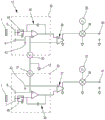
A circuit diagram 12 for an implementation of the present invention will now be described with reference to fig. 3.
The figure is based on the teaching of document FR2756048, to which reference can be made for implementation details.
The presented diagram comprises a plurality of parallel measurement paths. Fig. 3 shows an example with two measurement paths.
Each measurement path allows control and acquisition of measurements with respect to one or more electrodes and allows different excitation potentials to be generated for the electrodes.
Of course, the graph in FIG. 3 can be generalized to:
-implementing an arbitrary number of parallel measurement paths;
-implementing any number of different excitation potentials for different measurement paths;
-implementing a measurement path in parallel with the same excitation potential to allow to acquire several measurements simultaneously on electrodes polarized at the same excitation potential.
The diagram for the first measurement will now be described in detail, with reference numbers in parentheses corresponding to the second measurement path.
The detection electronics 12 include what is referred to as a "floating" portion 32(33) referenced to an excitation potential 42(43), which includes a first measurement level closest to the electrode. The excitation potential 42(43) is generated by a time-variable voltage source 30(31) referenced to the reference potential 13 of the electronic device 12.
The floating electronic device 32(33) mainly includes a charge amplifier 34(35) with a driving potential 42(43) as a reference. The charge amplifier 34(35) is connected at input to the measuring electrode 5 (7). This allows a voltage to be generated that is proportional to the accumulated charge in the electrode 5(7) that depends on the coupling capacitance generated by the object 1(9) in the vicinity of the electrode 5 (7).
The floating electronics 32(33) also include a multiplexer 44(45) or scanner that allows multiple electrodes 5(7) with a single measurement path to be "interrogated" in sequence. The multiplexer 44(45) is designed to connect the electrodes 5 (7):
-either to the input of a charge amplifier 34(35) to obtain a measurement result,
or to the reference potential 42(43), in which case the corresponding electrode behaves like the guard electrode 6(8), which allows to avoid parasitic capacitances with the active electrode connected to the input of the charge amplifier 34 (35).
The output signal of the charge amplifier 34(35) has the excitation potential 42(43) as a reference. Which is converted by the differential amplifier 36(37) into a signal with the reference potential 13 as a reference. Of course, the differential amplifier 36(37) can be replaced by any other component that allows the transfer of signals between electronic stages having different reference potentials.
The measurement signal is then demodulated by a demodulator 38(39) to produce a measurement 40(41) representative of the coupling or distance of the electrode 5(7) to the object 1 (9). In practice, the demodulator 38(39) is digital.
This detection principle allows to produce measurements with very high sensitivity and with very high accuracy, since all electronic components close to the electrode 5(7) are referenced to the excitation potential 42(43) and/or are polarized under the excitation potential 42 (43). Due to the structure of charge amplifier 34(35), electrode 5(7) is also polarized at excitation potential 42 (43). Therefore, parasitic capacitance can be prevented. In addition, a protection element (including the protection electrode 6(8)) polarized at the excitation potential 42(43) can be added near the measurement electrodes 5(7) or their connection tracks to avoid the occurrence of parasitic capacitances with neighboring elements subjected to another potential.
The electronics in fig. 3 can be implemented in the apparatus of fig. 1 such that, for example:
all electrodes of one face 4, 14 are controlled by the same electronic measuring path. Thus, according to the configuration shown, the first measuring path controls all the first electrodes 5 of the first face 6, while the second measuring path controls all the second electrodes 7 of the second face 14;
the electrodes of one face 4, 14 are distributed over the area and are controlled by several electronic measuring paths, respectively. This can allow for improved accuracy and independence of measurements in different regions;
the side electrodes 10, 11 are controlled by a first and a second measurement path, respectively;
the side electrodes 10, 11 are optionally connected to the first measurement path or to the second measurement path by switching means. Switching can be performed according to information items originating from other electrodes;
the side electrodes 10, 11 are controlled by a third electronic measuring path;
similarly, the electronics in fig. 3 can be implemented in the arrangement in fig. 2 such that, for example, all electrodes of the modules 21, 22 are controlled by the same electronic measurement path. Thus, according to the configuration shown, the first measurement path controls all the first electrodes 5 of the first module 21, while the second measurement path controls all the second electrodes 7 of the second module 22.
As previously mentioned, one subject of the present invention is to provide a method that allows managing a large number of detection areas, some of which may be strongly coupled with a user or a target.
According to a first variant embodiment of the invention, all the electrodes of one or more detection areas are switched to the reference potential 13 when taking measurements with the electrodes of another detection area. Thus, it is possible to avoid that the detection areas cause mutual interference by direct coupling as in the case of fig. 2 or by coupling with a command object as in the case of fig. 1.
More specifically, with reference to the illustration in fig. 2, this can advantageously be performed by switching the excitation potential 43 to, for example, the reference potential 13. In practice, this can be performed in particular by short-circuiting the voltage source 31, which means turning it off or generating a zero voltage. Therefore, all elements (including the protection element 8) referenced to the excitation potential 43 are set to the reference potential 13.
This first variant of the invention can be implemented in the embodiment of fig. 1 as follows:
the excitation potential 43 of the second electrode 7 is switched to the reference potential 13 to set the second electrode 7 of the second side 14 at the reference potential 13;
performing a measurement with the first electrode 5. Thus, even if the second electrode 7 is strongly coupled to the hand 9 of a user holding (for example) the second side 14 of the phone, the finger 1 can be detected with the first electrode 5 under optimal conditions, since the user is "seen" by these electrodes as being at the reference potential 13;
then, in the same way, the excitation potential 42 of the first electrode 5 is switched to the reference potential 13 to set the first electrode 5 of the first face 4 under the reference potential 13, and then the measurement is performed with the second electrode 7. Thus, the device can optionally be held and used on both faces in the same way.
The first variant of the invention can also be implemented in the embodiment of fig. 2 as follows:
the excitation potential 43 of the second electrode is switched to the reference potential 13 to set the second electrode 7 of the second module 22 at the reference potential 13;
performing a measurement with the first electrode 5 of the first module 21. These first electrodes 5 are therefore sensitive to the presence of the second module 22, including the second module 22 along the detection area 24, in the same way as the rest of the environment;
then, in the same way, the excitation potential 42 of the first electrode 5 is switched to the reference potential 13 to set the first electrode 5 of the first module 21 at this reference potential 13, and then the measurement is performed with the second electrode 7 of the second module 22.
Of course, all strategies for time multiplexing and scanning of different detection areas can be implemented within the scope of the invention.
However, this first variant of the invention has the disadvantage that the electrodes of the different detection areas have to be activated and interrogated in sequence.
A second variant, corresponding to a preferred embodiment of the invention, will now be given, which allows measurements to be performed simultaneously in several detection areas, while minimizing the risk of interference between these areas.
Referring to fig. 4, the (digitally) coupled signal is given the name Ve1(l) The coupled signal is obtained at the output 40 of the demodulator 38 of the first path of the detection electronics and provides a measurement result representing the capacitive coupling or distance between the first measuring electrode 5 and the target object 1.
More generally, the coupling signal originating from the path i ( i 1, 2 …) of the detection electronics is given the name Vei(l)。
Coupled signal Vei(l) As described below, with a duration greater than or equal to the measurement accumulation duration τ in the demodulator 38eThe time interval of (c) is updated. It can correspond to, for example:
a series of measurements taken with the same first electrode 5, or
Successive measurements taken with different first electrodes 5 polarized at the same reference potential 42 and switched by a multiplexer 44.
The analog charge measurement signal present at the output of the differential amplifier 36 and referenced to the reference potential 13 is given the designation Us1(t)。
More generally, the charge measurement signal of the path i (i ═ 1, 2, …) of the detection electronics is referred to as Usi(t)。
The charge measurement signal Usi(t) corresponds to the charge Q accumulated in the measuring electrode (i.e. electrode 5 for path i equal to 1)ei(t) and charge amplification gain GeiThe product of (a) and (b), i.e.,
Usi(t)=GeiQei(t) (equation 1)
Or at time intervals τsThe digital form of the sample is taken and,
Usi(k)=GeiQei(k) (formula 2)
The charge measurement signal is demodulated in demodulator 38 (for path 1) to obtain a coupled signal Vei(l) In that respect The demodulation is synchronous amplitude demodulation (low-pass filter and baseband transposition) in which the involved paths areThe excitation signal of the path is used as a local oscillator 30, 31. Which is performed digitally. Which includes a charge measurement signal Usi(k) Excitation signal V associated with corresponding path ii(k) Are multiplied by one another and during an accumulation time interval taueThe sum of the product terms above, i.e.,

Wherein k is 0 … Ns-1 and Ns=τe/τs。
Excitation signal Vi(k) Can be written as an amplitude term and a basis function b defining its temporal shapei(k) The general formula of the product of (a) is:
Vi(k)=|Vi|bi(k) in that respect (formula 4)
As mentioned before, the presence of an element polarized at a potential different from the reference potential 13 distorts the measurement result. These distortions can be modeled by an equivalent capacitance connecting the measuring electrodes to different interference voltage sources, mainly in parallel.
For example, in the case of FIG. 3, additional sources of electrical interference V are consideredpIn the presence of the target object 1, at a first excitation potential V1The charge measured on the polarized first electrode 5 at (t) can be expressed as follows:
Qe1(t)=C11V1(t)+C12V2(t)+C1pVp(t) (equation 5)
Capacitor C11Is the capacitance to be measured between the electrode 5 and the target object 1 which is considered to be at the reference potential 13. Capacitor C12For example due to the target object 1 and at the second excitation potential V2(t) parasitic capacitance due to local coupling between the polarized second electrode 7 (and the sustain electrode 8). Similarly, the capacitance C1pDue to interference with another electrical interference source VpParasitic capacitance due to coupling.
Additional sources of electrical interference VpCan be used for example for portable applicationsThe connection of the device to the charger results.
There may also be a voltage source at the target object 1, for example:
-a voltage source due to disturbances associated with its operation;
intentionally generating a voltage source for the operation of the target object in case, for example, the target object 1 is an active stylus polarized at its own excitation potential. This excitation potential of the stylus can then be selected to contribute to the measurement or to improve the measurement with at least one of the measurement paths or with several measurement paths in sequence. In this case, it can be synchronized with the excitation potential of the electrodes of the at least one measuring path.
The measured charge can be rewritten to a factorized digital form, i.e.,
Qe1(k)=Ce1[α11V1(k)+α12V2(k)+α1pVp(k)](formula 6)
By combining equation 6 and equation 3, an expression for the coupled signal is obtained:
Ve1(l)=Ge1Ce1Σk[α11V1(k)+α12V2(k)+α1pVp(k)]V1(k) (formula 7)
This expression can be rewritten as follows:
Ve1(l)=Ge1Ce1{α11ΣkV1(k)V1(k)
+α12ΣkV1(k)V2(k)
+α1pΣkV1(k)Vp(k) } (equation 8)
By substituting equation 4 into equation 8, an expression of the coupled signal is finally obtained:
Ve1(l)=Ge1Ce1{α11|V1|2Σkb1 2(k)
+α12|V1||V2|Σkb1(k)b2(k)
+α1pΣkV1(k)Vp(k) } (equation 9)
This expression can be generalized for any number i of excitation potentials V in the following formi:
Ve1(l)=Ge1Cei{αii|Vi|2Σkbi 2(k)
+Σj;j≠i(αij|Vi||Vj|∑kbi(k)bj(k))
+αipΣkVi(k)Vp(k) } (equation 10)
Coupling signal V dependent only on excitation potential iei(l) The first term of the general formula (iv) corresponds to the value of the desired measurement.
Dependent on a further excitation potential j or a further interference signal VpThe other term of (a) is a parasitic term, the effect of which must be minimized.
To simplify the labeling, the base function b can beiDimension N ofsDefines an inner product within the vector space such that:

Function biThe square of the modulus of (a) is then:

It can thus be seen that in order to couple signal VeiHas the least influence of interference in the general formula (1), the excitation signal ViMust be chosen such that two different basis functions bi、bjThe inner product (e.g. corresponding to different measurement paths) is negligible or larger than the excitation signal V of the electrode concernediBasis function b ofiIs at least much smaller than the square of the mode of (c):
|bi|>>bi·bj(formula 13)
Of course, if desired, at the excitation potential VjThe lower polarized electrode performs the measurement simultaneously, then the symmetry condition must also be satisfied:
|bj|>>bi·bj(formula 14)
The same reasoning can be applied for the interfering signal VpAs long as the signal can be sufficiently known (from theory or from measurement results). If the excitation signal V isiCan be selected such that it interacts with the interference signal VpIs negligible or is less than the excitation signal ViIs at least much smaller, its effect on the measurement results can be minimized.
All basis functions that allow these criteria to be met or at least approached can be used within the scope of the invention.
In order to ensure good independence of the signals detected by each measurement path i from the other terms, the basis functions biCan be chosen to obtain, for example, decibel ratios:

It is about-20 dB or less, or about-30 dB, or-40 dB or less. Thus, the interference on the coupled signal amplitude due to the parasitic sources does not exceed this decibel value.
The basis function can be a discrete function, which can take two values, e.g., +1 and-1.
The basis function can also be a discrete function, which can take a more complete set of discrete values, for example: + 1; 0;
0; -1。
-1。
by selecting adjacent values for the consecutive exponentials k, this allows for a better control of the resulting energy spectrum towards high frequencies. This also allows the generation of functions that approach pure sinusoids.
The criteria are given here by way of non-limiting example, which can be used to generate the basis functions:
-a basis function biCan be selected to produce a periodic square wave signal image, or close to a sinusoid. Then each basis function biCan mainly use the frequency fiTo represent;
it is then possible to choose the frequency fiSpaced apart from each other, or the frequencies can be selected in a suitable manner to obtain different basis functions bjOrthogonality therebetween;
for generating the two excitation potentials, it is possible to generate signals having the same frequency f1、f2But with a 90 degree phase shift of the signal. The signals are then in phase quadrature.
-a basis function biCan be selected to minimize energy peaks or to smooth the spectrum. A dispersion strategy may be used that can minimize the energy radiated by the device at some frequencies;
-a basis function biCan be selected to minimize energy at low frequencies where 1/f noise adversely affects the system; and/or in order to avoid energy at high frequencies due to electromagnetic compatibility or consumption;
for each of the above strategies, the choice may also be determined so as to withstand the parasitic interference VpThe inner product term of (a) is minimized to minimize its effect.
With regard to the implementation in a device,
-a basis function biCan be pre-computed and stored in the device, they can be used by the device in real time without additional computation;
several sets of functions can be made available in advance. The interference signal V can then be adjusted according to a criterionpTo select between these basis functions;
can be at the coupling signal Vei(l) Between successive acquisitions, thus if necessaryIf desired at period τeTo switch between different sets of basis functions. In the diagram of fig. 2, this means that the shape of the signal generated by the excitation sources 30, 31 is changed over time, or that different excitation sources 30, 31 are switched. The entire device can thus be dynamically reconfigured according to its environment.
It should be noted that the variant embodiment in which the electrodes are polarized at the reference potential 13 complies with the criterion for the generation of a polarization potential that minimizes the inner product of the cross terms. In fact, if biIs a basis function of the polarization potential of the electrode used for the measurement, and bjIs the basis function of the electrode at the reference potential, then bj=0,bi·bj0 and thus according to equation 13, | bi|>>bi·bj。
Of course, in this case, simultaneous measurement with the electrode polarized at the reference potential 13 is not performed, so that the symmetry condition of equation 14 does not have to be satisfied.
By way of application example, the invention can be carried out under the following conditions:
τs=5μs
τe=8ms
Ns=1600
in particular, excitation potential families can also be generated in which k is 0 … Ns-1:
-having two different and orthogonal frequencies:
b1(k) 1 ═ 1; + 1; -1; -1; + 1; + 1; -1; -1; … repeat 199 times;
b2(k) 1 ═ 1; + 1; + 1; + 1; -1; -1; -1; -1; … repeated 199 times.
-having two identical frequencies and orthogonal signals:
b1(k) 1 ═ 1; + 1; -1; -1; + 1; + 1; -1; -1; … repeat 199 times;
b2(k) -1; + 1; + 1; -1; -1; + 1; + 1; -1; … repeated 199 times.
Of course, the invention is not limited to the examples that have just been described and many modifications can be made to these examples without departing from the scope of the invention.
Claims (20)
1. A method for capacitive detection implementing a plurality of electrodes (5, 7) capable of allowing detection of one or more objects (1, 21, 22) capacitively coupled to a ground potential and in the vicinity of the plurality of electrodes by capacitive coupling, characterized in that the method comprises:
forming a first set of electrodes (5) of the plurality of electrodes along a first region of the device having a reference potential (13);
forming a second set of electrodes (7) of the plurality of electrodes along a second region of the device;
polarizing a second set of electrodes (7) on the second area at a second excitation potential (43) generated by a second floating electronic device (33) referenced to a second voltage source (31) referenced to the reference potential (13);
a first set of electrodes (5) on the first area is simultaneously polarized at a first excitation potential (42) generated by a first floating electronic device (32) referenced to a first voltage source (30) referenced to a reference potential (13) such that the inner product of the first and second excitation potentials (42, 43) is zero for a predetermined duration.
2. The method of claim 1, wherein the first and second excitation potentials (42, 43) comprise at least one excitation potential that is variable over time.
3. The method of one of the preceding claims, wherein the first and second excitation potentials (42, 43) comprise periodic excitation potentials having different frequencies.
4. The method of claim 1 or 2, wherein the first and second excitation potentials (42, 43) comprise at least one excitation potential whose frequency components are spread over a spectral band.
5. The method of claim 1 or 2, wherein the first and second excitation potentials (42, 43) comprise two periodic excitation potentials of the same frequency and in phase quadrature.
6. The method of claim 1 or 2, wherein the first and second excitation potentials (42, 43) comprise at least one excitation potential whose inner product with an interference signal is minimized.
7. The method of claim 1 or 2, wherein the first and second excitation potentials (42, 43) comprise at least one excitation potential substantially equal to the reference potential.
8. The method of claim 1 or 2, further comprising the step of measuring the capacitive coupling of the electrodes (5, 7), the step comprising:
-obtaining a measurement representative of the charge of said electrode, and
-demodulating the measurement representative of said electric charge by using an excitation potential (42, 43) of said electrode (5, 7).
9. The method of claim 1, wherein the first area is on a first surface (4) of the device and the second area is on a second surface (14) of the device, wherein the first surface is different from the second surface.
10. The method of claim 1, wherein the first region is on a first surface (4) of the device and the second region is on a second surface (14) of the device, wherein the first surface and the second surface are on different sides of the device.
11. A device for capacitive detection having a reference potential (13), comprising a plurality of electrodes (5, 7) capable of allowing detection of one or more objects (1, 21, 22) capacitively coupled to a ground potential and in the vicinity of the plurality of electrodes by capacitive coupling, characterized in that the device further comprises:
at least a first region and a second region of the apparatus, the plurality of electrodes being formed at least along the first region and the second region, a second set of electrodes of the plurality of electrodes on the second region being configured to be polarised at a second excitation potential (43) generated by a second floating electronic device (33) referenced to a second voltage source (31) referenced to the reference potential (13); and
an excitation unit (30, 31) capable of simultaneously polarizing a first set of electrodes of the plurality of electrodes (5, 7) on a first area at a first excitation potential (42) generated by a first floating electronic device (32) referenced to a first voltage source (30) referenced to a reference potential (13) such that an inner product of the first and second excitation potentials (42, 43) is zero for a predetermined duration.
12. The device according to claim 11, further comprising a measuring unit (34, 35, 36, 37) referenced to an excitation potential (42, 43) polarizing the connected electrode (5, 7).
13. The device according to claim 12, further comprising a demodulation unit (38, 39) connected to the measurement unit (34, 35, 36, 37) and capable of generating a measurement representative of the capacitive coupling referenced to the reference potential (13).
14. The device according to one of claims 11 to 13, further comprising means allowing to polarize at least one electrode at an excitation potential:
at several different excitation potentials (42, 43), and/or
-at least one excitation potential (42, 43) or at the reference potential (13).
15. The device of claim 11, wherein the first area is on a first surface (4) of the device and the second area is on a second surface (14) of the device, wherein the first surface is different from the second surface.
16. The device of claim 11, wherein the first region is on a first surface (4) of the device and the second region is on a second surface (14) of the device, wherein the first surface and the second surface are on different sides of the device.
17. An electronic device comprising an apparatus for capacitive detection according to one of claims 11 to 16 and implementing the method of any one of claims 1 to 10.
18. An electronic device as claimed in claim 17, wherein the first region is on a first surface (4) of the apparatus, and wherein the second region is on a second surface (14) opposite the first surface.
19. The electronic device of claim 18, which is one of the following types: smart phones, input boards.
20. An electronic device as claimed in claim 17, comprising a plurality of modules (21, 22) which are displaceable relative to one another, each module comprising an electrode (5, 7) which is polarized at an excitation potential (42, 43) which is different from the other modules (21, 22).
Applications Claiming Priority (3)
| Application Number | Priority Date | Filing Date | Title |
|---|---|---|---|
| FR1353371A FR3004551A1 (en) | 2013-04-15 | 2013-04-15 | MULTIZONE CAPACITIVE DETECTION METHOD, DEVICE AND APPARATUS USING THE METHOD |
| FR1353371 | 2013-04-15 | ||
| PCT/EP2014/057158 WO2014170180A2 (en) | 2013-04-15 | 2014-04-09 | Method of multi-zone capacitive sensing, device and apparatus implementing the method |
Publications (2)
| Publication Number | Publication Date |
|---|---|
| CN105452998A CN105452998A (en) | 2016-03-30 |
| CN105452998B true CN105452998B (en) | 2020-05-19 |
Family
ID=49322456
Family Applications (1)
| Application Number | Title | Priority Date | Filing Date |
|---|---|---|---|
| CN201480027820.8A Expired - Fee Related CN105452998B (en) | 2013-04-15 | 2014-04-09 | Method for multizone capacitive sensing, device and apparatus for carrying out the method |
Country Status (7)
| Country | Link |
|---|---|
| US (1) | US10592046B2 (en) |
| EP (1) | EP2987056A2 (en) |
| JP (1) | JP6284623B2 (en) |
| KR (1) | KR101911135B1 (en) |
| CN (1) | CN105452998B (en) |
| FR (1) | FR3004551A1 (en) |
| WO (1) | WO2014170180A2 (en) |
Families Citing this family (32)
| Publication number | Priority date | Publication date | Assignee | Title |
|---|---|---|---|---|
| US7920129B2 (en) | 2007-01-03 | 2011-04-05 | Apple Inc. | Double-sided touch-sensitive panel with shield and drive combined layer |
| US20090174676A1 (en) | 2008-01-04 | 2009-07-09 | Apple Inc. | Motion component dominance factors for motion locking of touch sensor data |
| FR2949007B1 (en) | 2009-08-07 | 2012-06-08 | Nanotec Solution | DEVICE AND METHOD FOR CONTROL INTERFACE SENSITIVE TO A MOVEMENT OF A BODY OR OBJECT AND CONTROL EQUIPMENT INCORPORATING THIS DEVICE. |
| FR2976688B1 (en) | 2011-06-16 | 2021-04-23 | Nanotec Solution | DEVICE AND METHOD FOR GENERATING AN ELECTRICAL POWER SUPPLY IN AN ELECTRONIC SYSTEM WITH A VARIABLE REFERENCE POTENTIAL. |
| FR2985049B1 (en) | 2011-12-22 | 2014-01-31 | Nanotec Solution | CAPACITIVE MEASURING DEVICE WITH SWITCHED ELECTRODES FOR TOUCHLESS CONTACTLESS INTERFACES |
| US9336723B2 (en) | 2013-02-13 | 2016-05-10 | Apple Inc. | In-cell touch for LED |
| FR3005763B1 (en) | 2013-05-17 | 2016-10-14 | Fogale Nanotech | DEVICE AND METHOD FOR A CAPACITIVE CONTROL INTERFACE ADAPTED TO THE IMPLEMENTATION OF ELECTRODES OF HIGHLY RESISTIVE MEASUREMENTS |
| KR101984443B1 (en) | 2013-12-13 | 2019-05-30 | 애플 인크. | Integrated touch and display architectures for self-capacitive touch sensors |
| WO2015175013A1 (en) | 2014-05-16 | 2015-11-19 | Wrostix Technologies Llc | Structure for integrated touch screen |
| WO2015178920A1 (en) | 2014-05-22 | 2015-11-26 | Onamp Research Llc | Panel bootstrapping architectures for in-cell self-capacitance |
| FR3028061B1 (en) * | 2014-10-29 | 2016-12-30 | Fogale Nanotech | CAPACITIVE SENSOR DEVICE COMPRISING ADJUSTED ELECTRODES |
| FR3028062B1 (en) * | 2014-10-29 | 2018-01-12 | Fogale Nanotech | CAPACITIVE CONTROL INTERFACE DEVICE INTEGRATED WITH A DISPLAY SCREEN |
| WO2016072983A1 (en) | 2014-11-05 | 2016-05-12 | Onamp Research Llc | Common electrode driving and compensation for pixelated self-capacitance touch screen |
| CN107209602B (en) | 2015-02-02 | 2020-05-26 | 苹果公司 | Flexible self-capacitance and mutual capacitance touch sensing system architecture |
| FR3032287B1 (en) | 2015-02-04 | 2018-03-09 | Quickstep Technologies Llc | MULTILAYER CAPACITIVE DETECTION DEVICE, AND APPARATUS COMPRISING THE DEVICE |
| US10146359B2 (en) | 2015-04-28 | 2018-12-04 | Apple Inc. | Common electrode auto-compensation method |
| US10386962B1 (en) | 2015-08-03 | 2019-08-20 | Apple Inc. | Reducing touch node electrode coupling |
| US10642426B2 (en) * | 2015-12-23 | 2020-05-05 | Lg Chem, Ltd. | Touch screen sensor |
| FR3051896B1 (en) * | 2016-05-25 | 2018-05-25 | Fogale Nanotech | CAPACITIVE DETECTION DEVICE WITH NULL GUARD |
| CN109564485B (en) | 2016-07-29 | 2022-04-01 | 苹果公司 | Touch sensor panel with multi-power domain chip configuration |
| US10642418B2 (en) | 2017-04-20 | 2020-05-05 | Apple Inc. | Finger tracking in wet environment |
| FR3066131B1 (en) * | 2017-05-15 | 2019-06-14 | Fogale Nanotech | ROBOT WITH CAPACITIVE DETECTION |
| FR3070022B1 (en) * | 2017-08-10 | 2020-11-06 | Fogale Nanotech | CAPACITIVE DRESSING ELEMENT FOR ROBOT, ROBOT EQUIPPED WITH SUCH A DRESSING ELEMENT |
| FR3070294B1 (en) * | 2017-08-28 | 2021-01-22 | Fogale Nanotech | MULTI-DISTANCE DETECTION DEVICE FOR A ROBOT, AND ROBOT EQUIPPED WITH SUCH DEVICE (S) |
| US11086463B2 (en) | 2017-09-29 | 2021-08-10 | Apple Inc. | Multi modal touch controller |
| WO2019067267A1 (en) | 2017-09-29 | 2019-04-04 | Apple Inc. | Multi-power domain touch sensing |
| FR3081223B1 (en) * | 2018-05-15 | 2020-09-18 | Fogale Nanotech | PARALLEL REDUNDANT CAPACITIVE DETECTION DEVICE |
| FR3081224B1 (en) * | 2018-05-15 | 2020-06-12 | Fogale Nanotech | REDUNDANT CAPACITIVE DETECTION DEVICE SERIES |
| FR3083729B1 (en) * | 2018-07-13 | 2020-07-10 | Fogale Nanotech | APPARATUS PROVIDED WITH CAPACITIVE DETECTION AND ELECTRICAL LINE (S) IN THE DETECTION AREA |
| US11016616B2 (en) | 2018-09-28 | 2021-05-25 | Apple Inc. | Multi-domain touch sensing with touch and display circuitry operable in guarded power domain |
| FR3106002B1 (en) * | 2020-01-08 | 2022-01-28 | Fogale Nanotech | Capacitive sensing device comprising an induction bias module |
| US11662867B1 (en) | 2020-05-30 | 2023-05-30 | Apple Inc. | Hover detection on a touch sensor panel |
Citations (3)
| Publication number | Priority date | Publication date | Assignee | Title |
|---|---|---|---|---|
| WO2012009493A2 (en) * | 2010-07-16 | 2012-01-19 | Perceptive Pixel Inc. | Capacitive touch sensor having code-divided and time-divided transmit waveforms |
| WO2012063520A1 (en) * | 2010-11-12 | 2012-05-18 | Sharp Kabushiki Kaisha | Linear system coefficient estimating method, linear device column value estimating method, capacitance detecting method, integrated circuit, touch sensor system, and electronic device |
| EP2477101A2 (en) * | 2011-01-13 | 2012-07-18 | Samsung Electronics Co., Ltd | Apparatus and method of identifying touch area |
Family Cites Families (64)
| Publication number | Priority date | Publication date | Assignee | Title |
|---|---|---|---|---|
| US5483261A (en) | 1992-02-14 | 1996-01-09 | Itu Research, Inc. | Graphical input controller and method with rear screen image detection |
| US5488204A (en) | 1992-06-08 | 1996-01-30 | Synaptics, Incorporated | Paintbrush stylus for capacitive touch sensor pad |
| US5880411A (en) | 1992-06-08 | 1999-03-09 | Synaptics, Incorporated | Object position detector with edge motion feature and gesture recognition |
| GB9406702D0 (en) | 1994-04-05 | 1994-05-25 | Binstead Ronald P | Multiple input proximity detector and touchpad system |
| US5825352A (en) | 1996-01-04 | 1998-10-20 | Logitech, Inc. | Multiple fingers contact sensing method for emulating mouse buttons and mouse operations on a touch sensor pad |
| US5835079A (en) | 1996-06-13 | 1998-11-10 | International Business Machines Corporation | Virtual pointing device for touchscreens |
| US8421776B2 (en) * | 1996-08-12 | 2013-04-16 | Elo Touch Solutions, Inc. | Acoustic condition sensor employing a plurality of mutually non-orthogonal waves |
| FR2756048B1 (en) | 1996-11-15 | 1999-02-12 | Nanotec Ingenierie | FLOATING CAPACITIVE MEASUREMENT BRIDGE AND ASSOCIATED MULTI-CAPACITIVE MEASUREMENT SYSTEM |
| US6310610B1 (en) | 1997-12-04 | 2001-10-30 | Nortel Networks Limited | Intelligent touch display |
| US7663607B2 (en) | 2004-05-06 | 2010-02-16 | Apple Inc. | Multipoint touchscreen |
| US8479122B2 (en) | 2004-07-30 | 2013-07-02 | Apple Inc. | Gestures for touch sensitive input devices |
| KR100595912B1 (en) | 1998-01-26 | 2006-07-07 | 웨인 웨스터만 | Method and apparatus for integrating manual input |
| US6188391B1 (en) | 1998-07-09 | 2001-02-13 | Synaptics, Inc. | Two-layer capacitive touchpad and method of making same |
| JP4542637B2 (en) | 1998-11-25 | 2010-09-15 | セイコーエプソン株式会社 | Portable information device and information storage medium |
| KR100427162B1 (en) * | 1999-09-27 | 2004-04-14 | 시티즌 도케이 가부시키가이샤 | Method for driving color liquid crystal display panel and method for control of display of time piece |
| US6847354B2 (en) | 2000-03-23 | 2005-01-25 | The United States Of America As Represented By The Administrator Of The National Aeronautics And Space Administration | Three dimensional interactive display |
| EP1211633B1 (en) * | 2000-11-28 | 2004-06-09 | STMicroelectronics S.r.l. | Texile-like capacitive pressure sensor and method of mapping the pressure exerted at points of a surface of a flexible and pliable object, particularly of a sail |
| JP3800984B2 (en) | 2001-05-21 | 2006-07-26 | ソニー株式会社 | User input device |
| CN1636163A (en) * | 2001-06-20 | 2005-07-06 | 赛特勒有限公司 | Thin planar switches and their applications |
| JP2003173237A (en) | 2001-09-28 | 2003-06-20 | Ricoh Co Ltd | Information input-output system, program and storage medium |
| US6690387B2 (en) | 2001-12-28 | 2004-02-10 | Koninklijke Philips Electronics N.V. | Touch-screen image scrolling system and method |
| US11275405B2 (en) * | 2005-03-04 | 2022-03-15 | Apple Inc. | Multi-functional hand-held device |
| FR2844048B1 (en) | 2002-08-30 | 2005-09-30 | Nanotec Solution | SYSTEM AND METHOD FOR NON-CONTACT MEASUREMENT OF RELATIVE DISPLACEMENT OR POSITIONING OF TWO ADJACENT OBJECTS BY CAPACITIVE PATH, AND APPLICATION TO MIRROR CONTROL |
| FR2844349B1 (en) | 2002-09-06 | 2005-06-24 | Nanotec Solution | CAPACITIVE SENSOR PROXIMITY DETECTOR |
| WO2006043660A1 (en) * | 2004-10-22 | 2006-04-27 | Sharp Kabushiki Kaisha | Display device with touch sensor, and drive method for the device |
| JP4541124B2 (en) * | 2004-12-15 | 2010-09-08 | パナソニック株式会社 | Plasma display device |
| FR2884349B1 (en) | 2005-04-06 | 2007-05-18 | Moving Magnet Tech Mmt | BITABLE POLARIZED ELECTROMAGNETIC ACTUATOR WITH QUICK ACTUATION |
| FR2888319B1 (en) | 2005-07-07 | 2008-02-15 | Nanotec Solution Soc Civ Ile | METHOD FOR NON-CONTACT MEASUREMENT OF RELATIVE DISPLACEMENT OR RELATIVE POSITIONING OF A FIRST OBJECT IN RELATION TO A SECOND OBJECT INDUCINGLY. |
| US7599670B2 (en) * | 2005-07-21 | 2009-10-06 | Microsoft Corporation | Dynamic bias for receiver controlled by radio link quality |
| FR2893711B1 (en) | 2005-11-24 | 2008-01-25 | Nanotec Solution Soc Civ Ile | DEVICE AND METHOD FOR CAPACITIVE MEASUREMENT BY FLOATING BRIDGE |
| US20080047764A1 (en) * | 2006-08-28 | 2008-02-28 | Cypress Semiconductor Corporation | Temperature compensation method for capacitive sensors |
| US7986193B2 (en) * | 2007-01-03 | 2011-07-26 | Apple Inc. | Noise reduction within an electronic device using automatic frequency modulation |
| US8054299B2 (en) * | 2007-01-08 | 2011-11-08 | Apple Inc. | Digital controller for a true multi-point touch surface useable in a computer system |
| JP4967780B2 (en) * | 2007-04-20 | 2012-07-04 | セイコーエプソン株式会社 | Coordinate input device and display device |
| US8373665B2 (en) * | 2007-07-26 | 2013-02-12 | International Business Machines Corporation | Interactive display device |
| US8232977B2 (en) * | 2007-11-14 | 2012-07-31 | N-Trig Ltd. | System and method for detection with a digitizer sensor |
| KR101237640B1 (en) | 2008-01-29 | 2013-02-27 | (주)멜파스 | Touchscreen apparatus having structure for preventing forming of parasitic capacitance |
| EP2291729B1 (en) | 2008-04-30 | 2013-06-05 | N-Trig Ltd. | Multi-touch detection |
| US20090277696A1 (en) * | 2008-05-09 | 2009-11-12 | Reynolds Joseph K | Gradient sensors |
| JP2010061405A (en) | 2008-09-03 | 2010-03-18 | Rohm Co Ltd | Capacitance sensor, detection circuit thereof, input device, and control method of capacity sensor |
| US8638314B2 (en) * | 2008-10-17 | 2014-01-28 | Atmel Corporation | Capacitive touch buttons combined with electroluminescent lighting |
| US9244562B1 (en) * | 2009-07-31 | 2016-01-26 | Amazon Technologies, Inc. | Gestures and touches on force-sensitive input devices |
| GB0913734D0 (en) | 2009-08-06 | 2009-09-16 | Binstead Ronald P | Masked touch sensors |
| FR2948997B1 (en) | 2009-08-07 | 2012-04-20 | Nanotec Solution | CAPACITIVE PRESSURE SENSOR INCLUDING TEMPERATURE MEASUREMENT COMPATIBLE WITH HOT ENVIRONMENTS. |
| FR2949007B1 (en) | 2009-08-07 | 2012-06-08 | Nanotec Solution | DEVICE AND METHOD FOR CONTROL INTERFACE SENSITIVE TO A MOVEMENT OF A BODY OR OBJECT AND CONTROL EQUIPMENT INCORPORATING THIS DEVICE. |
| FR2949008B1 (en) | 2009-08-07 | 2011-09-16 | Nanotec Solution | CAPACITIVE DETECTION DEVICE WITH FUNCTION INTEGRATION. |
| EP2465021A4 (en) * | 2009-08-12 | 2014-06-25 | Cirque Corp | Synchronous timed orthogonal measurement pattern for multi-touch sensing on a touchpad |
| KR101625611B1 (en) * | 2009-09-03 | 2016-06-14 | 삼성디스플레이 주식회사 | Touch panel and touch input/output apparatus having the same |
| US9753586B2 (en) * | 2009-10-08 | 2017-09-05 | 3M Innovative Properties Company | Multi-touch touch device with multiple drive frequencies and maximum likelihood estimation |
| US8810524B1 (en) * | 2009-11-20 | 2014-08-19 | Amazon Technologies, Inc. | Two-sided touch sensor |
| TW201124766A (en) | 2010-01-08 | 2011-07-16 | Wintek Corp | Display device with touch panel |
| CN101840294B (en) * | 2010-01-21 | 2012-01-18 | 宸鸿科技(厦门)有限公司 | Method for scanning projective capacitive touch panel |
| US9092129B2 (en) * | 2010-03-17 | 2015-07-28 | Logitech Europe S.A. | System and method for capturing hand annotations |
| US8923014B2 (en) | 2010-08-19 | 2014-12-30 | Lg Display Co., Ltd. | Display device having touch panel |
| FR2971066B1 (en) | 2011-01-31 | 2013-08-23 | Nanotec Solution | THREE-DIMENSIONAL MAN-MACHINE INTERFACE. |
| JP5350437B2 (en) * | 2011-06-27 | 2013-11-27 | シャープ株式会社 | Touch sensor system |
| EP2761757A4 (en) * | 2011-10-01 | 2015-04-15 | Intel Corp | Digital fractional frequency divider |
| KR20130057637A (en) | 2011-11-24 | 2013-06-03 | 삼성전기주식회사 | Touch sensing apparatus |
| FR2990020B1 (en) | 2012-04-25 | 2014-05-16 | Fogale Nanotech | CAPACITIVE DETECTION DEVICE WITH ARRANGEMENT OF CONNECTION TRACKS, AND METHOD USING SUCH A DEVICE. |
| CN103593096A (en) * | 2012-08-16 | 2014-02-19 | 瀚宇彩晶股份有限公司 | Capacitance typed touch control system |
| US9411474B2 (en) | 2012-11-15 | 2016-08-09 | Nokia Technologies Oy | Shield electrode overlying portions of capacitive sensor electrodes |
| US9088282B2 (en) * | 2013-01-25 | 2015-07-21 | Apple Inc. | Proximity sensors with optical and electrical sensing capabilities |
| TWI483169B (en) * | 2013-06-11 | 2015-05-01 | Pixart Imaging Inc | Capacitance detecting circuit and power supplying apparatus utilizing the capacitance detecting circuit |
| US20160001496A1 (en) * | 2014-07-01 | 2016-01-07 | Preco, Inc. | Methods and apparatus for the fabrication of pattern arrays in making touch sensor panels |
-
2013
- 2013-04-15 FR FR1353371A patent/FR3004551A1/en active Pending
-
2014
- 2014-04-09 KR KR1020157031159A patent/KR101911135B1/en active IP Right Grant
- 2014-04-09 US US14/784,264 patent/US10592046B2/en not_active Expired - Fee Related
- 2014-04-09 WO PCT/EP2014/057158 patent/WO2014170180A2/en active Application Filing
- 2014-04-09 EP EP14724650.8A patent/EP2987056A2/en not_active Withdrawn
- 2014-04-09 JP JP2016508091A patent/JP6284623B2/en not_active Expired - Fee Related
- 2014-04-09 CN CN201480027820.8A patent/CN105452998B/en not_active Expired - Fee Related
Patent Citations (3)
| Publication number | Priority date | Publication date | Assignee | Title |
|---|---|---|---|---|
| WO2012009493A2 (en) * | 2010-07-16 | 2012-01-19 | Perceptive Pixel Inc. | Capacitive touch sensor having code-divided and time-divided transmit waveforms |
| WO2012063520A1 (en) * | 2010-11-12 | 2012-05-18 | Sharp Kabushiki Kaisha | Linear system coefficient estimating method, linear device column value estimating method, capacitance detecting method, integrated circuit, touch sensor system, and electronic device |
| EP2477101A2 (en) * | 2011-01-13 | 2012-07-18 | Samsung Electronics Co., Ltd | Apparatus and method of identifying touch area |
Also Published As
| Publication number | Publication date |
|---|---|
| KR101911135B1 (en) | 2018-10-23 |
| CN105452998A (en) | 2016-03-30 |
| US20160034102A1 (en) | 2016-02-04 |
| KR20150143543A (en) | 2015-12-23 |
| FR3004551A1 (en) | 2014-10-17 |
| JP2016515744A (en) | 2016-05-30 |
| WO2014170180A2 (en) | 2014-10-23 |
| JP6284623B2 (en) | 2018-02-28 |
| WO2014170180A3 (en) | 2014-12-04 |
| US10592046B2 (en) | 2020-03-17 |
| EP2987056A2 (en) | 2016-02-24 |
Similar Documents
| Publication | Publication Date | Title |
|---|---|---|
| CN105452998B (en) | Method for multizone capacitive sensing, device and apparatus for carrying out the method | |
| US10579849B2 (en) | Methods and sensors for multiphase scanning in the fingerprint and touch applications | |
| JP6568205B2 (en) | Capacitance-based touch device and method with reduced interference | |
| CN106990880B (en) | Method and apparatus for improved capacitive sensing detection | |
| EP3035168B1 (en) | Pen input device, method for correcting input coordinate thereof and electronic device for supporting the same | |
| KR102270454B1 (en) | Capacitive touch sensor system and method | |
| CN107924260B (en) | Multiphase fingerprint sensor layout and building | |
| KR101579351B1 (en) | Capacitivebased touch apparatus and method therefor with reduced interference | |
| CN105874412B (en) | Use the capacitive touch system and method for difference signal technique | |
| US9104278B2 (en) | Capacitance-type proximity sensor device and electronic apparatus using the same | |
| KR101769889B1 (en) | System and method for the generation of a signal correlated with a manual input operation | |
| JP6042763B2 (en) | Display device with touch detection function and electronic device | |
| US20160209947A1 (en) | Noise cancellation tecnique for capacitive touchscreen controller using differential sensing | |
| US10222913B2 (en) | Device for contactless interaction with an electronic and/or computer apparatus, and apparatus equipped with such a device | |
| JP2015099462A (en) | Coordinate input device and mobile terminal | |
| WO2007135663A1 (en) | Variable capacitor array | |
| US20160179247A1 (en) | Guard accessory device for an electronic and/or computer apparatus, and apparatus equipped with such an accessory device | |
| US10816582B2 (en) | Sigma-delta configurations for capacitance sensing | |
| KR102349856B1 (en) | Touch input device | |
| WO2019118077A1 (en) | Capacitive motion sensor | |
| CN108073322A (en) | The interference of active pen panel receiver eliminates | |
| JP5899698B2 (en) | Human body part position measuring device and electronic device system | |
| CN106020578A (en) | Single receiver superdoze mode | |
| JP6772658B2 (en) | Capacitive input device | |
| KR20210040254A (en) | Input sensing using overlapping code division multiplexing (cdm) |
Legal Events
| Date | Code | Title | Description |
|---|---|---|---|
| C06 | Publication | ||
| PB01 | Publication | ||
| C10 | Entry into substantive examination | ||
| SE01 | Entry into force of request for substantive examination | ||
| GR01 | Patent grant | ||
| GR01 | Patent grant | ||
| CF01 | Termination of patent right due to non-payment of annual fee |
Granted publication date: 20200519 |