CN1033547C - An operational transconductance amplifier with matched outputs - Google Patents
An operational transconductance amplifier with matched outputs Download PDFInfo
- Publication number
- CN1033547C CN1033547C CN94191359A CN94191359A CN1033547C CN 1033547 C CN1033547 C CN 1033547C CN 94191359 A CN94191359 A CN 94191359A CN 94191359 A CN94191359 A CN 94191359A CN 1033547 C CN1033547 C CN 1033547C
- Authority
- CN
- China
- Prior art keywords
- mirror circuit
- current mirror
- auxiliary
- circuit
- output
- Prior art date
- Legal status (The legal status is an assumption and is not a legal conclusion. Google has not performed a legal analysis and makes no representation as to the accuracy of the status listed.)
- Expired - Fee Related
Links
Images

Classifications
-
- H—ELECTRICITY
- H03—ELECTRONIC CIRCUITRY
- H03F—AMPLIFIERS
- H03F3/00—Amplifiers with only discharge tubes or only semiconductor devices as amplifying elements
- H03F3/34—Dc amplifiers in which all stages are dc-coupled
- H03F3/343—Dc amplifiers in which all stages are dc-coupled with semiconductor devices only
- H03F3/347—Dc amplifiers in which all stages are dc-coupled with semiconductor devices only in integrated circuits
-
- H—ELECTRICITY
- H03—ELECTRONIC CIRCUITRY
- H03F—AMPLIFIERS
- H03F3/00—Amplifiers with only discharge tubes or only semiconductor devices as amplifying elements
- H03F3/68—Combinations of amplifiers, e.g. multi-channel amplifiers for stereophonics
Abstract
A multi-output integrated circuit amplifier (500) consists of a first primary current mirror (510), and a plurality of secondary current mirrors (520). The first primary current mirror (510) implemented in a single substrate and having a first primary input (511). The first primary current mirror (510) generates a plurality of first inverted primary current outputs in response to a first current signal coupled to the first primary input (511). The plurality of secondary current mirrors are implemented in the same single substrate and each has a secondary input coupled to a unique one of the plurality of primary current outputs of the first primary current mirror (510), each of said plurality of secondary current mirrors (520) having a gain, and each of said plurality of secondary current mirrors (520) generating an inverted secondary current output signal, the magnitude of which is determined substantially by the unique one of the plurality of primary current outputs coupled thereto and the gain thereof.
Description
The present invention relates to electronic amplifier circuit, particularly have the current amplifier circuit of a plurality of outputs.
Portable by battery-operated product such as radio frequency communication devices, as to wish to have possibility minimum total power consumption is so that extending battery life.Also wish to operate this product, so that their total power consumption reduces to minimum degree with possible minimum voltage.
Conventional radio frequency communication devices can use one or several to use special integrated circuit and realize that function such as phase-locked loop is with composite number word logic or the required frequency of radio circuit.For saving power, a synthesizer or other circuit of realizing in using special integrated circuit generally should use alap voltage power supply.In addition, in order to save power more, these circuit can (send or receive, storage, retrieval or demonstration) one or several circuit connection, and turn-off during " sleep " or " rest " with battery saving mode work as signal during effective processing cycle.Work by this way, the product of portable battery-operated can increase available battery life significantly, therefore obtains at radio frequency communication devices such as cell phone etc. more " speech time " being arranged.
In the past, the low voltage circuit of realizing in the integrated circuit of using particularly is generally by bipolar simulation or I
2L (integrated injection logic) logical circuit constitutes.There are some problems in these bipolar circuits, as the high-speed computation (I of each gate circuit 0.25 μ A work of difference
2L is general only at 50KH
2About work), lack dynamic range (saturation point of conventional low voltage dipole analog circuit is generally 20mV, obtains scope less than 600mV from one volt of power supply) and their intrinsic operating characteristic and change greatly with temperature.
In view of the above, need low voltage cmos (complementary metal oxide semiconductors (CMOS)) technical process and suitable circuit layout technology now, the designer can use the special integrated circuit of the application in radio frequency communication devices to obtain analog-and digital-two functions.Like this, the low voltage cmos design can be operated in the power level lower significantly than comparable bipolar design.In addition, when working with battery saving mode, power can be more effectively saved in the CMOS design, and the circuit performance characteristic of improvement is provided simultaneously.
According to a first aspect of the invention, many outputs integrated amplifier is by the first principal current mirror circuit (current mirror) and a plurality of auxiliary current mirror circuit.The first principal current mirror circuit is made of the complementary metal oxide semiconductor field effect transistor of realizing in the monolithic substrate, has one first primary input end.Response is coupling in first current signal of first input end, and the first principal current mirror circuit produces a plurality of first reverse principal current output.A plurality of auxiliary current mirror circuits are made of the complementary metal oxide semiconductor field effect transistor of realizing in identical monolithic substrate, its each an auxiliary input is all arranged, the output of a uniqueness that should auxiliary input be connected to a plurality of principal current outputs of the first principal current mirror circuit, each circuit of described a plurality of auxiliary current mirror circuits all has a gain, and each circuit of described a plurality of auxiliary current mirror circuits produces a reverse auxiliary current output signal, and its amplitude is determined by the output and the gain thereof of a uniqueness that is coupled to a plurality of principal current outputs basically.
Fig. 1 illustrates the block diagram that is fit to the radio-frequency (RF) communication system used with the present invention.
Fig. 2 illustrates the block diagram that Fig. 1 is fit to the radiophone in the system shown in Figure 1 that the present invention uses.
Fig. 3 is illustrated in the block diagram that is fit to the selective call receiver in the system shown in Figure 1 that the present invention uses.
Fig. 4 illustrates the electrical block diagram of the many outputs operation transconductance amplifier that is used for Wireless Telecom Equipment in an alternative embodiment of the invention.
Fig. 5 illustrates the electrical block diagram of the many outputs operation transconductance amplifier that is used for Wireless Telecom Equipment in the preferred embodiments of the present invention.
Referring to Fig. 1, the preferred embodiment of wireless communication system comprises a telephone set 101, public switch telephone network (PSTN) by routine is connected to a system controller 102, it can monitor the operation of radio frequency sending set/receiver 103, and coding and decoding immigration and the departure address be and corresponding land line and cellular radio addressing require the form of compatibility.System controller 102 also can play a part the beep-page message that coding is used to transmit by radio frequency sending set/receiver 103.Telephone signal by at least one antenna transmission that is connected to radio frequency sending set/receiver to and receive from radiophone 105.Radio frequency sending set/receiver 103 also can be used for sending beep-page message to an optional selective call receiver 106.
Be noted that system controller 102 can be in the transmission that the distributes middle work that controls environment, this environment allow hybrid cellular, with broadcast, wide territory and local master/slave or any routine cover scheme.In addition, those skilled in the art will recognize that this phone and paging function can reside in separately the system controller, can be independently or with network's mode work.
Referring to Fig. 2, show the block diagram of the radiophone of battery 201 power supplies.Radiofrequency signal is received with carrier frequency and/or is sent by antenna 202.This antenna is received a receiver 203 and a transmitter 204 by a duplexer 205.The signal that receives is by receiver 203 filtering and demodulation, and the signal of demodulation is received control circuit 206 from receiver 203, is used to recover to be included in the interior any information of received signal.Control circuit 206 also uses a phase-locked loop frequency synthesizer to produce the reference frequency of local oscillator, but also produces the filtering in a plurality of filter control signal receiver control 230 that are coupled to receiver 203.The information of Hui Fuing is used to start a reminiscences 207 (situation at cellular radiotelephone is a ringer) by control circuit then, and supporting telephone connects after replying this calling.When the phone connection was finished, this user can carry out audio communication with the opposing party through loud speaker 208 and microphone 209.The sound that control circuit 206 sends recovery is to loud speaker 208, and loud speaker 208 is an acoustic energy with transformation of electrical energy, thereby makes this user can hear any communication.It is electric energy that microphone 209 is used for conversion acoustic energy, is used to modulate the radio-frequency carrier that is produced by transmitter 204 by control circuit 206.
This user can begin by the number of selecting suitable controller 210 and input will get in touch a side to call out.When input and transmission, this number can appear in the demonstration 211 and provide visual feedback to the user, confirms the number of being imported and send subsequently.
Referring to Fig. 3, the block diagram of the selective call receiver of battery 312 power supplies is shown.This selective call receiver work is so that through antenna 313 received signals.The signal that is received sends to receiver 314 from antenna 313.Receiver 314 work is so that the signal that uses routine techniques filtering and demodulation to be received, and the signal that transmits demodulation is to control circuit 315, control circuit 315 decodings and recover to be included in the interior information of received signal.Control circuit 315 also uses phase-locked loop frequency synthesizer to produce the local oscillator reference frequency, is coupled to a plurality of filter control signals that receiver 315 is used for being controlled at the filtering of receiver 315 but also produce.Control 316 according to the information and the user that recover, this selective call receiver is such as utilizing display 317 can show at least a portion of this information, and can receive through detectable prompting 318 these message of signaling user.
In the two preferred embodiment of radiophone and selective call receiver, relevant control circuit 206,315 can comprise a little processing or application-specific integrated circuit (ASIC), it realizes that this voltage regulator can provide the other parts of the voltage of adjusting to wireless device such as the signal multiplexer of a signal processor (for example decoder), a routine, the function of a voltage regulator.Alternately, relevant control circuit 206,315 can comprise such characteristic, as A/D, D/A converter, programmable I/O port, control bus is as being used for the environment measuring circuit of light or temperature conditions, audio power amplifying circuit, control interface circuit, clock or local oscillator frequencies synthesizer and display brightness circuit.Typically these unit with conventional method assembling so that the radiophone that comprises customer requirements or the marketable characteristic of selective call receiver to be provided.
Referring to Fig. 4, show the electrical block diagram of many outputs operation transconductance amplifier (OTA) 400 according to another embodiment of the invention, the display 317 and the display 211 that are used for above-mentioned communication equipment (selective call receiver 106 and portable wireless telephone), described is another embodiment with OTA400 of a plurality of outputs of the present invention.Another one of the present invention as described herein implements to be used to drive the row and column of LCD 317 pixels, wherein requires a plurality of outputs, but should be understood that OTA400 can be used for other function.Circuit input signal is received the circuit input 410 of many outputs OTA400.Circuit input 410 is the differential inputs with a positive input 412 and a negative input 411.Differential input signal cross-couplings is to the differential input level positive input 416 (being labeled as Pin among Fig. 4) and the negative input of level 415 (being labeled as Min) of a plurality of OTA amplifiers 420 among Fig. 4.Each OTA amplifier 420 produces a non-return single-ended output signal at a plurality of output 430 ends, and its amplitude is relevant with the gain of each OTA amplifier 420.Output signal is coupled to the row of LCD 317.This differential input signal also is directly coupled to the differential input level positive input 416 and the negative input 415 of level of a plurality of OTA amplifiers 440.Each OTA amplifier produces a reverse single-ended output signal in a plurality of outputs 450, and its amplitude is relevant with the gain of each OTA amplifier 440.These output signals are coupled to the row of LCD 317.The transistor that these output signals are connected on by control in mode well-known in the art in the output stage of OTA level 420 and 440 switches on and off.
Can know that the output signal 430 of OTA is reverse with respect to the output signal of OTA440.
Know that also this grade input and this circuit input 410 can be single-ended, rather than differential input, OTA420 and 440 is single-ended input stage and output stage in this case.In addition, when circuit input 410 was as shown in Figure 4 differential input, one or several OTA level can be differential input level and output stage, thereby one or several differential output 430 and 450 is provided.OAT420 and 440 comprises the mos field effect transistor (MOSFET) with series connection output stage, and its design is well known in the art, and these MOSFET are preferably on the same substrate.In this another embodiment of the present invention, each OTA420 and 440 has transadmittance gain and the skew of being determined by the configuration of transistor geometries, interconnection and material variables.Wish that typically the design skew is minimum.The offset error that each OTA has a gain error and is offset with respect to design with respect to designing gain, typically they are different along with difference output.
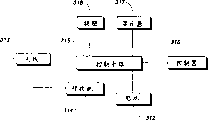
Referring to Fig. 5 the electrical block diagram of many outputs operation transconductance amplifier (OTA) 500 according to a preferred embodiment of the invention is shown, this OTA500 is used in the above-mentioned communication equipment (selective call receiver 106 and portable wireless telephone), and it has a plurality of outputs.The preferred embodiments of the present invention described here are FILTER TO CONTROL amplifiers, the frequency synthesizer that is used for control circuit 206 and 315, the wherein error signal of the filtering that produces by the phase-locked loop frequency synthesizer circuit input of being coupled to this filtering control amplifier, and the current control oscillator input of this phase-locked loop is coupled in an output of this FILTER TO CONTROL amplifier.In this purposes, the preferred embodiments of the present invention have a plurality of booster amplifier outputs, they must be coupled to the output of the different gains of current control oscillator output with tight tracking, and they are coupled to receiver 315, are used for the filtering of receiver control 315.Can know that this amplifier can be used for other function equivalently, as the row and column of the pixel that drives LCD 317.
In a preferred embodiment of the invention, the error signal of filtering is coupled to the circuit input 501 of input OTA505.Circuit input 501 is differential inputs, comprises positive input 502 and negative input 503.Input OTA505 is an OTA level, and the voltage that responds this circuit input signal produces first current signal.This first current signal is coupled to first primary input of the first principal current mirror 510, responds first current signal and drive a plurality of first main output stage from the mirror output driver signal that produces in the first primary mirror level, produces a plurality of first reverse main output signals 550.The auxiliary input that the first reverse main output signal is coupled to each auxiliary current mirror circuit 520, all mirror image circuit all have identical basic gain.The reverse auxiliary output signal 550 that each auxiliary current mirror circuit 520 produces a plurality of parallel connections is so that produce single output signal, its amplitude basically by the first principal current output signal that is connect, it gains substantially and progression in parallel is determined.Can see that in Fig. 5 utilize the progression in each auxiliary current mirror circuit 520 parallel connection, to used example, the relative gain ratio of shown reverse auxiliary output signal is 2: 3: 4: 5 here.One of auxiliary output signal is connected to the current control oscillator in the phase-locked loop.Other auxiliary output signal is received receiver 315, is used for the filtering of receiver control 315.
One of first reverse main output current signal is received second primary input of the second principal current mirror circuit 530, and current mirroring circuit 530 responds the first primary input signal, produces a plurality of second reverse main output signals 550 by drive a plurality of second main output stage from the mirror output driver signal that produces in the second primary mirror circuit stages.The auxiliary input that the first reverse main output signal is coupled to each auxiliary current mirror circuit 540, this current mirroring circuit 540 all has identical basic gain.Each auxiliary current mirror circuit 540 produces a plurality of reverse auxiliary output signal in parallel so that produce single output signal, and the first principal current output signal that its amplitude is connect basically, it gains substantially and progression in parallel is determined.Can see that in Fig. 5 utilize the progression in each auxiliary current mirror circuit 540 parallel connection, to used example, the relative gain ratio of shown reverse auxiliary output signal is 1: 2: 3 here.These auxiliary output signals are also received receiver 315, are used for the filtering of receiver control 315.
Auxiliary current mirror circuit 520 and 540 auxiliary output signal can switch on and off by the transistor of connecting in the output stage that is controlled at auxiliary current mirror circuit 520 and 540, and this carries out in mode well known in the art.Can know, the auxiliary output signal of auxiliary current mirror circuit 520 is reverse with respect to the auxiliary output signal of auxiliary current mirror circuit 540, with in the application that does not require reverse output signal, do not need the second primary mirror circuit 530 and a plurality of auxiliary mirror circuit 540.
Know that also input OTA505 has an output, it is the first differential current signal, and under this situation, the first primary mirror circuit is a differential input current mirror circuit.Know that also the first principal current mirror circuit 510 can have an output, it is the differential reverse first main output current signal, and under this situation, second primary input of the auxiliary input of auxiliary current mirror circuit 520 and the second primary mirror circuit is differential input.Know that also the second principal current mirror circuit 530 can have an output, it is the differential reverse second main output current signal, and in this case, the auxiliary input of auxiliary current mirror circuit 540 is differential inputs.
OTA505, principal current mirror circuit 510 and 530 and auxiliary mirror circuit 520 and 540 comprise mos field effect transistor (MOSFET) with cascade output stage, its design is well known in the art, MOSFET is in identical substrate 595.
Can know, because auxiliary current mirror circuit 520 shared identical OTA505 and identical principal current mirror circuit 510, by they one of a plurality of auxiliary output that produces owing to the error in principal current mirror circuit 510 has common gain error, and owing to principal current mirror circuit 512 also has common offset error.Transadmittance gain between the output of auxiliary mirror circuit 520 is than being that the precision that conforms to auxiliary current mirror circuit 520 is relevant, and they are designed and can be manufactured have a higher consistent precision than what a plurality of OTA of use such as OTA400 may accomplish.
Know that also in utilizing single input stage, the preferred embodiments of the present invention have reduced input capacitance, therefore produce the higher input impedance of narrating in an alternative embodiment of the invention such as narration here of a plurality of OTA.
As in the above the preferred embodiments of the present invention being narrated, the identical reverse auxiliary output signal of a plurality of parallel connections produces the high output that conforms to, but lower here precision is acceptable, can adopt the auxiliary mirror circuit (wherein utilize comprise have the transistorized single auxiliary mirror circuit output stage of corresponding different geometries obtain different gains) of scale that some economy in the integrated circuit layout area are provided.
Therefore, can see, unique combination of the first principal current mirror circuit and a plurality of auxiliary circuit mirror circuits on same substrate, optional single input amplifier and the second optional principal current mirror circuit provide the trsanscondutance amplifier of a computing, this amplifier has a plurality of outputs, has different gains but accurate consistent gain and offset error.
Claims (7)
1. output integrated amplifier more than a kind is characterized in that, comprising:
The first principal current mirror circuit of realizing in the monolithic substrate has the first primary input end, and first current signal of the first primary input end is coupled in described first principal current mirror circuit response, produces a plurality of first reverse principal current output; With
A plurality of auxiliary current mirror circuits of in this monolithic substrate, realizing, each mirror circuit has the auxiliary input of output of a uniqueness of a plurality of principal current outputs that are connected to the described first principal current mirror circuit, each mirror circuit of described a plurality of auxiliary current mirror circuits has a gain, produce a reverse auxiliary current output signal with each auxiliary current mirror circuit of described a plurality of auxiliary current mirror circuits, its amplitude is determined by the electric current output and the gain thereof of a uniqueness of a plurality of principal currents outputs that connect basically.
2. according to many outputs integrated amplifier of claim 1, it is characterized in that, further comprise:
The second principal current mirror circuit of in this monolithic substrate, realizing, it has the second primary input end of output of a uniqueness of a plurality of reverse first principal current output that is coupled to the described first principal current mirror circuit, first current signal of the first primary input end of the first principal current mirror circuit is coupled in response, and the described second principal current mirror circuit produces a plurality of second principal current output signals.
3. according to many outputs integrated amplifier of claim 2, it is characterized in that, further comprise:
One or several auxiliary current mirror circuit of in the monolithic substrate, realizing, each mirror circuit has the auxiliary input of a unique output of a plurality of principal current outputs that are connected to the described second principal current mirror circuit, each mirror circuit of described one or several auxiliary current mirror circuit has a gain, described one or several auxiliary current mirror circuit produces a reverse auxiliary current output signal, and its amplitude is determined by the unique output of this one or several principal current output that is connected to described auxiliary current mirror circuit and the gain of described auxiliary current mirror circuit basically.
4. according to many outputs integrated amplifier of claim 1, it is characterized in that, further comprise:
An input amplifier of in this monolithic substrate, realizing, it has a circuit input end and is an output of first current signal, first current signal is coupled to the first principal current mirror circuit input, described input amplifier response is connected to this circuit input signal voltage of this circuit input end, produces this first current signal.
5. according to many outputs integrated amplifier of claim 1, it is characterized in that, the first principal current mirror circuit is complementary mirror circuit amplifier, and the first primary input end is that a differential input terminal and one or several first reverse principal current output signal are the first reversing differential principal current output signals.
6. according to many outputs integrated amplifier of claim 1, it is characterized in that, one or several auxiliary current mirror circuit is complementary mirror circuit amplifier, should auxiliary input be that a differential input terminal and one or several reverse auxiliary current output signal are reverse differential auxiliary current output signals.
7. according to many outputs integrated amplifier of claim 1, it is characterized in that this circuit input signal is coupled from a phase-locked loop frequency synthesizer, this frequency synthesizer is included in the control circuit that is used for Wireless Telecom Equipment.
Applications Claiming Priority (2)
| Application Number | Priority Date | Filing Date | Title |
|---|---|---|---|
| US08/152,991 | 1993-11-10 | ||
| US08/152,991 US5363061A (en) | 1993-11-10 | 1993-11-10 | Operational transconductance amplifier with matched outputs |
Publications (2)
| Publication Number | Publication Date |
|---|---|
| CN1118641A CN1118641A (en) | 1996-03-13 |
| CN1033547C true CN1033547C (en) | 1996-12-11 |
Family
ID=22545326
Family Applications (1)
| Application Number | Title | Priority Date | Filing Date |
|---|---|---|---|
| CN94191359A Expired - Fee Related CN1033547C (en) | 1993-11-10 | 1994-11-10 | An operational transconductance amplifier with matched outputs |
Country Status (6)
| Country | Link |
|---|---|
| US (1) | US5363061A (en) |
| EP (1) | EP0678225A4 (en) |
| KR (2) | KR960700561A (en) |
| CN (1) | CN1033547C (en) |
| CA (1) | CA2153253A1 (en) |
| WO (1) | WO1995013654A1 (en) |
Families Citing this family (4)
| Publication number | Priority date | Publication date | Assignee | Title |
|---|---|---|---|---|
| US5598129A (en) * | 1995-08-24 | 1997-01-28 | Motorola, Inc. | Low current drain operational transconductance amplifier |
| EP1410618B1 (en) | 2001-06-08 | 2009-08-19 | Broadcom Corporation | Integrated upstream amplifier for cable modems and cable set-top boxes |
| US20060091534A1 (en) * | 2002-12-13 | 2006-05-04 | Matsushita Electric Industrial Co., Ltd. | Chip part manufacturing method and chip parts |
| CN101917168B (en) * | 2010-06-30 | 2013-02-27 | 西安电子科技大学 | High switching rate transconductance amplifier for active power factor corrector |
Family Cites Families (4)
| Publication number | Priority date | Publication date | Assignee | Title |
|---|---|---|---|---|
| JPH0775322B2 (en) * | 1990-02-22 | 1995-08-09 | 富士通株式会社 | Semiconductor integrated circuit device |
| JP3031419B2 (en) * | 1990-06-13 | 2000-04-10 | 三菱電機株式会社 | Semiconductor integrated circuit |
| US5165054A (en) * | 1990-12-18 | 1992-11-17 | Synaptics, Incorporated | Circuits for linear conversion between currents and voltages |
| US5142696A (en) * | 1991-04-16 | 1992-08-25 | Motorola, Inc. | Current mirror having increased output swing |
-
1993
- 1993-11-10 US US08/152,991 patent/US5363061A/en not_active Expired - Fee Related
-
1994
- 1994-11-10 CN CN94191359A patent/CN1033547C/en not_active Expired - Fee Related
- 1994-11-10 CA CA002153253A patent/CA2153253A1/en not_active Abandoned
- 1994-11-10 WO PCT/US1994/013081 patent/WO1995013654A1/en not_active Application Discontinuation
- 1994-11-10 EP EP95901882A patent/EP0678225A4/en not_active Withdrawn
- 1994-11-10 KR KR1019950702844A patent/KR960700561A/en not_active IP Right Cessation
- 1994-11-10 KR KR1019950702844A patent/KR0140268B1/en active
Also Published As
| Publication number | Publication date |
|---|---|
| EP0678225A4 (en) | 1999-11-03 |
| US5363061A (en) | 1994-11-08 |
| EP0678225A1 (en) | 1995-10-25 |
| KR960700561A (en) | 1996-01-20 |
| KR0140268B1 (en) | 1998-07-15 |
| CN1118641A (en) | 1996-03-13 |
| WO1995013654A1 (en) | 1995-05-18 |
| CA2153253A1 (en) | 1995-05-18 |
Similar Documents
| Publication | Publication Date | Title |
|---|---|---|
| US5548246A (en) | Power amplifier including an impedance matching circuit and a switch FET | |
| US6781455B2 (en) | High efficiency power amplifier | |
| KR950010252B1 (en) | The power amplifier | |
| JP3103712B2 (en) | Power amplifier and amplification method | |
| US6329875B1 (en) | Power amplifier, power control method for power amplifier, and communication equipment | |
| CN1087521C (en) | Method and apparatus for amplifying signal | |
| CN1034381C (en) | A differential amplifier with common mode bias | |
| KR20040092489A (en) | Audio signal amplifier circuit and electronic apparatus having the same | |
| CN1033547C (en) | An operational transconductance amplifier with matched outputs | |
| CN1067194C (en) | Output stage of operational amplifier suitable for mounting on substrate and method of amplifying therewith | |
| US5640681A (en) | Boot-strapped cascode current mirror | |
| US20050186934A1 (en) | Semiconductor integrated circuit | |
| US5412336A (en) | Self-biasing boot-strapped cascode amplifier | |
| CN1050720C (en) | Communication apparatus utilizing high power amplifier | |
| JPH06196955A (en) | Power amplifier | |
| JPH09181642A (en) | Communication terminal equipment | |
| CN217470274U (en) | Loudspeaker system | |
| KR100256972B1 (en) | Method and apparatus for improving efficiency of power amp | |
| JPH01140817A (en) | High frequency power control circuit | |
| EP0942570A2 (en) | Portable communication device with a loudspeaker having a double functionality | |
| KR20040003617A (en) | Variable impedance power amplifier module | |
| KR100442201B1 (en) | Variable impedance power amplifier module | |
| KR200200416Y1 (en) | Converting circuit for mike and speaker | |
| JPH03289802A (en) | Electronic circuit | |
| JPH05327578A (en) | Portable telephone set |
Legal Events
| Date | Code | Title | Description |
|---|---|---|---|
| C06 | Publication | ||
| PB01 | Publication | ||
| C10 | Entry into substantive examination | ||
| SE01 | Entry into force of request for substantive examination | ||
| C14 | Grant of patent or utility model | ||
| GR01 | Patent grant | ||
| C19 | Lapse of patent right due to non-payment of the annual fee | ||
| CF01 | Termination of patent right due to non-payment of annual fee |