CN102955343A - Illumination device and display device - Google Patents
Illumination device and display device Download PDFInfo
- Publication number
- CN102955343A CN102955343A CN2012102809702A CN201210280970A CN102955343A CN 102955343 A CN102955343 A CN 102955343A CN 2012102809702 A CN2012102809702 A CN 2012102809702A CN 201210280970 A CN201210280970 A CN 201210280970A CN 102955343 A CN102955343 A CN 102955343A
- Authority
- CN
- China
- Prior art keywords
- light
- lighting device
- optical
- laser
- phase
- Prior art date
- Legal status (The legal status is an assumption and is not a legal conclusion. Google has not performed a legal analysis and makes no representation as to the accuracy of the status listed.)
- Pending
Links
Images


Classifications
-
- G—PHYSICS
- G02—OPTICS
- G02B—OPTICAL ELEMENTS, SYSTEMS OR APPARATUS
- G02B5/00—Optical elements other than lenses
- G02B5/18—Diffraction gratings
- G02B5/1866—Transmission gratings characterised by their structure, e.g. step profile, contours of substrate or grooves, pitch variations, materials
- G02B5/1871—Transmissive phase gratings
-
- G—PHYSICS
- G02—OPTICS
- G02B—OPTICAL ELEMENTS, SYSTEMS OR APPARATUS
- G02B27/00—Optical systems or apparatus not provided for by any of the groups G02B1/00 - G02B26/00, G02B30/00
- G02B27/10—Beam splitting or combining systems
- G02B27/1006—Beam splitting or combining systems for splitting or combining different wavelengths
- G02B27/102—Beam splitting or combining systems for splitting or combining different wavelengths for generating a colour image from monochromatic image signal sources
- G02B27/1026—Beam splitting or combining systems for splitting or combining different wavelengths for generating a colour image from monochromatic image signal sources for use with reflective spatial light modulators
- G02B27/1033—Beam splitting or combining systems for splitting or combining different wavelengths for generating a colour image from monochromatic image signal sources for use with reflective spatial light modulators having a single light modulator for all colour channels
-
- G—PHYSICS
- G02—OPTICS
- G02B—OPTICAL ELEMENTS, SYSTEMS OR APPARATUS
- G02B27/00—Optical systems or apparatus not provided for by any of the groups G02B1/00 - G02B26/00, G02B30/00
- G02B27/10—Beam splitting or combining systems
- G02B27/14—Beam splitting or combining systems operating by reflection only
- G02B27/141—Beam splitting or combining systems operating by reflection only using dichroic mirrors
-
- G—PHYSICS
- G02—OPTICS
- G02B—OPTICAL ELEMENTS, SYSTEMS OR APPARATUS
- G02B27/00—Optical systems or apparatus not provided for by any of the groups G02B1/00 - G02B26/00, G02B30/00
- G02B27/48—Laser speckle optics
-
- G—PHYSICS
- G03—PHOTOGRAPHY; CINEMATOGRAPHY; ANALOGOUS TECHNIQUES USING WAVES OTHER THAN OPTICAL WAVES; ELECTROGRAPHY; HOLOGRAPHY
- G03B—APPARATUS OR ARRANGEMENTS FOR TAKING PHOTOGRAPHS OR FOR PROJECTING OR VIEWING THEM; APPARATUS OR ARRANGEMENTS EMPLOYING ANALOGOUS TECHNIQUES USING WAVES OTHER THAN OPTICAL WAVES; ACCESSORIES THEREFOR
- G03B21/00—Projectors or projection-type viewers; Accessories therefor
- G03B21/14—Details
- G03B21/20—Lamp housings
- G03B21/2006—Lamp housings characterised by the light source
- G03B21/2033—LED or laser light sources
-
- G—PHYSICS
- G03—PHOTOGRAPHY; CINEMATOGRAPHY; ANALOGOUS TECHNIQUES USING WAVES OTHER THAN OPTICAL WAVES; ELECTROGRAPHY; HOLOGRAPHY
- G03B—APPARATUS OR ARRANGEMENTS FOR TAKING PHOTOGRAPHS OR FOR PROJECTING OR VIEWING THEM; APPARATUS OR ARRANGEMENTS EMPLOYING ANALOGOUS TECHNIQUES USING WAVES OTHER THAN OPTICAL WAVES; ACCESSORIES THEREFOR
- G03B21/00—Projectors or projection-type viewers; Accessories therefor
- G03B21/14—Details
- G03B21/20—Lamp housings
- G03B21/208—Homogenising, shaping of the illumination light
-
- H—ELECTRICITY
- H04—ELECTRIC COMMUNICATION TECHNIQUE
- H04N—PICTORIAL COMMUNICATION, e.g. TELEVISION
- H04N9/00—Details of colour television systems
- H04N9/12—Picture reproducers
- H04N9/31—Projection devices for colour picture display, e.g. using electronic spatial light modulators [ESLM]
- H04N9/3141—Constructional details thereof
- H04N9/315—Modulator illumination systems
- H04N9/3161—Modulator illumination systems using laser light sources
Abstract
The invention discloses an illumination device and a display device. The illumination device includes: a light source section including a laser light source; an optical element disposed on an optical path of a laser light beam emitted from the laser light source, branching an optical path of an incident light beam incident thereon into a plurality of optical paths, and allowing branched light beams to be output therefrom; an optical member receiving the branched light beams that travel along the plurality of optical paths, and allowing illumination light to be output therefrom based on the branched light beams; and a driver section driving the optical element to allow phases of the branched light beams to be changed independently of one another. The display device comprises a light modulation element and the illumination device. The invention achieves the compactness as well as improves the utilization efficiency of light while reducing the generation of interference patterns (or improving display image quality).
Description
The cross reference of related application
The application comprises the relevant theme of the disclosed content of Japanese priority patent application JP 2011-180779 of submitting to Japan Office with on August 22nd, 2011, therefore incorporates by reference the full content of this Japanese priority application into this paper.
Technical field
The present invention relates to the lighting device of luminous (comprise and send laser) and utilize such lighting device to show the display device of image.
Background technology
Usually, projector (or projection display equipment) comprises the optical module as critical piece, and this optical module is comprised of the lamp optical system that comprises light source (or lighting device) and the projection optical system (or projection optics system) that comprises optical modulation element.In the field of this projector, it is day by day universal in recent years, to be known as the light and handy portable projection instrument of small-sized (or the hand size) of " micro projector ".Usually, this micro projector mainly comprises light emitting diode (LED) as light source in its lighting device.
On the other hand, people are interested gradually recently is as the new type light source in the lighting device laser instrument.For instance, as the projector that uses three primary colors (for example red (R), green (G) and blue (B)) laser, present known the projector that is equipped with gas laser arranged.The clear 55-65940 communique of Japanese Patent Application Laid-Open and the flat 06-208089 communique of Japanese Patent Application Laid-Open have disclosed and have used as previously mentioned laser instrument as the example of the projection of light source instrument.By using laser instrument as light source, projector has been realized the color reproduction of wide region and low energy consumption.
Usually, when shining on the scattering surface such as coherent lights such as laser, just can observe hot spot pattern (spotty pattern) on this scattering surface, this situation from the light that uses other kinds is different.Such pattern is known as " speckle pattern (speckle pattern) ".When above-mentioned illumination was mapped on the scattering surface, by randomly scattering, mutually interfered by the scattered light with random phase (these phase places are lip-deep slight uneven corresponding with this) at each diverse location place of scattering surface for this light.As a result, produced speckle pattern.
If what use is the projector that has laser instrument in its light source, then above-mentioned speckle pattern (or interference pattern) can overlap onto on the image that is shown on the screen.These patterns can be identified by the human eye into strong random noise (random noise), thereby have caused the reduction of image quality.The speckle pattern that generates by this way may become shortcoming common when utilizing coherent laser as light source.Therefore, various trials have been carried out to reduce the generation of such speckle pattern (speckle noise) at present.
For example, the clear 55-65940 of above-mentioned document Japanese Patent Application Laid-Open has disclosed the projector that has laser instrument in its light source, and in this projector, piezoelectric element makes the screen slight vibration in order to reduce the generation of above-mentioned speckle pattern.Usually, the flicker on the image in human eye and human brain are difficult to identify during about 20ms to 50ms.Therefore, human eye carries out integration with the vibration in the image interior between such short-term, and this equalization value is identified as image.Therefore, thus this projector is intended to allow a large amount of independently speckle pattern be overlapped in the degree that on the screen above-mentioned speckle noise equalization almost can not be recognized this speckle noise to human eye between this short-term.Yet, owing to need to allow large screen self vibrate slightly, so this technology may cause the structure large-scale in the projector.
Simultaneously, the flat 06-208089 of above-mentioned document Japanese Patent Application Laid-Open has disclosed such projector: wherein, dispersing element is mechanically rotated, thereby allow speckle pattern be shifted at high speed on screen, make thus Human Perception less than speckle noise.Yet, because this dispersing element is used to scattered light, so this technology may reduce the utilization ratio of light.
Summary of the invention
Therefore, expectation can realize miniaturization and improve lighting device and the display device of the utilization ratio of light in the generation that reduces interference pattern.
One embodiment of the invention provides a kind of lighting device, and described lighting device comprises: light source portion, and described light source portion comprises LASER Light Source; Optical element, described optical element is arranged on the light path of the laser beam that sends from described LASER Light Source, described optical element is separated into a plurality of light paths to the light path that is incident to the incident beam on the described optical element, and makes light beam after the separation from described optical element outgoing; Optics, described optics receive the light beam after the described separation of propagating along described a plurality of light paths, and based on the light beam after the described separation from described optics outgoing illumination light; And drive division, described drive division drives described optical element, so that the phase place of the light beam after the described separation changes independently of each other.
Another embodiment of the present invention provides a kind of display device, and described display device is provided with lighting device and optical modulation element.Described optical modulation element is modulated the illumination light that obtains from described lighting device based on picture signal.Described lighting device comprises: light source portion, and described light source portion comprises LASER Light Source; Optical element, described optical element is arranged on the light path of the laser beam that sends from described LASER Light Source, described optical element is separated into a plurality of light paths to the light path that is incident to the incident beam on the described optical element, and makes light beam after the separation from described optical element outgoing; Optics, described optics receive the light beam after the described separation of propagating along described a plurality of light paths, and based on the light beam after the described separation from described optics outgoing illumination light; And drive division, described drive division drives described optical element, so that the phase place of the light beam after the described separation changes independently of each other.
In the above-mentioned lighting device and display device of respectively implementing the shape case of the present invention, be arranged at described optical element on the light path of laser beam and be separated into a plurality of light paths by the light path with incident beam and make light beam after the separation from described optical element outgoing.In addition, described drive division drives this optical element so that the phase place of the light beam after the described separation of propagating along described a plurality of light paths changes independently of each other.Therefore, reduced the generation of the interference pattern that causes because of laser.In addition, described optics receives the light beam after the described separation, and based on the light beam after the described separation by illumination light from described optics outgoing.Therefore, even when above-mentioned optical element is driven, still can reduces or prevent when light loss that light beam produces when described optical element enters described optics (in other words, reducing or prevent the coupling loss of each light beam after separating).
The lighting device of above-mentioned each embodiment of the present invention and display device are provided with optical element and optics, described optical element is separated into a plurality of light paths to the light path of incident beam (comprising laser beam), and makes light beam after the separation from described optical element outgoing; Described optics receives the light beam after the described separation, and from described optics outgoing illumination light.In addition, described optical element is actuated to so that the phase place of the light beam after the described separation changes independently of each other.Therefore, in the generation that has reduced the interference pattern that causes because of laser, the light loss that reduces or prevented from producing when described optical element enters described optics when light beam.So, can in the generation (perhaps improving image quality) that reduces interference pattern, realize miniaturization and improve the utilization ratio of light.
It will be appreciated that top generality explanation and following detailed description all are exemplary, and all are intended to provide further explanation for the present invention's technology required for protection.
Description of drawings
Here provide accompanying drawing in order to further understand the present invention, these accompanying drawings are merged in this instructions and consist of the part of this instructions.These accompanying drawings illustrate embodiment, and are used for explaining principle of the present invention with this instructions.
Fig. 1 illustrates the one-piece construction of the display device of embodiment of the present invention.
Fig. 2 is the synoptic diagram of the far-field pattern of the laser beam that sends from LASER Light Source for explanation.
Fig. 3 (A) part and (B) part be the synoptic diagram that the intensity distributions of the laser beam that sends from LASER Light Source has been described.
Fig. 4 is the synoptic diagram that the basic function of optical element shown in Fig. 1 has been described.
Fig. 5 A and Fig. 5 B are the synoptic diagram that illustrates the exemplary detailed structure of optical element shown in Fig. 4.
Fig. 6 (A) part and (B) part be the synoptic diagram that the diffraction function that is realized by optical element shown in Fig. 4 has been described.
Fig. 7 (A) part and (B) part be the synoptic diagram that the overlaying function of diffraction light has been described.
Fig. 8 is the synoptic diagram that illustrates the exemplary detailed structure of fly's-eye lens shown in Fig. 1.
Fig. 9 illustrates the one-piece construction according to the display device of comparative example 1.
Figure 10 is the synoptic diagram that illustrates the exemplary vibration operation of optical element.
Figure 11 (A) part to (C) part is to have illustrated within vibration operating period of the optical element shown in Figure 10, the synoptic diagram that changes from the phase place of the light (diffraction light) of this optical element outgoing.
Figure 12 A and Figure 12 B illustrate the structure of the optical element of embodiment 1.
Figure 13 A to Figure 13 C illustrates the diffraction characteristic of the optical element of embodiment 1.
Figure 14 is the synoptic diagram of structure that illustrates the interference pattern measuring system of embodiment 2.
Figure 15 has illustrated the view field of embodiment 2 and the synoptic diagram of the relation between the measured zone.
(A) part of Figure 16 to (D) part is the performance plot that illustrates the interference pattern measurement result of comparative example 2 and embodiment 2.
Figure 17 A to Figure 17 C is the synoptic diagram of exemplary vibration operation that illustrates the optical element of variation 1.
Figure 18 illustrates the structure of optical element of variation 2 and the synoptic diagram of function.
Figure 19 (A) part and (B) part be the synoptic diagram that illustrates the detailed structure of the phase-change element shown in Figure 18 (phase change element).
Figure 20 (A) part and (B) part be the synoptic diagram that illustrates the detailed structure of the prism array shown in Figure 18.
Figure 21 A and Figure 21 B are respectively the synoptic diagram that the basic function of the basic function of the phase-change element shown in Figure 19 and the prism array shown in Figure 20 has been described.
Figure 22 illustrates the structure of optical element of variation 3 and the synoptic diagram of function.
Embodiment
Below, describe with reference to the accompanying drawings embodiment of the present invention in detail.It should be noted that according to following order and describe.
1, embodiment (using diffraction element as the example of optical element)
2, embodiment (according to embodiment 1 and the embodiment 2 of embodiment)
3, variation
Variation 1 (optical element with the plane of its light shaft positive cross in another example of vibrating of direction)
Variation 2 (using phase-change element and prism array as the example of optical element)
Variation 3 (using liquid crystal cell and prism array as the example of optical element)
Other variation
One, embodiment
1) unitary construction of display device 3
Fig. 1 illustrates the unitary construction of the display device (display device 3) of embodiment of the present invention.This display device 3 is that image (or optical imagery) is projected projection display equipment on the screen 30 (or projecting plane).Particularly, display device 3 comprises lighting device 1 and utilizes the illumination light of lighting device 1 to show the optical system (or display optical system) of image.
In the above construction, for example, each all is when being made of semiconductor laser as red laser instrument 11R, green laser 11G and blue laser 11B, far-field pattern (the far field pattern of the laser beam that sends from them; FFP) for example as shown in Figure 2.More specifically, the FFP of the laser beam (red laser light beam Lr, green laser beam Lg or blue laser beams Lb) that sends from semiconductor laser is ellipse or analogous shape, rather than circular (isotropy).
As mentioned above, for example, each all is when being made of semiconductor laser as red laser instrument 11R, green laser 11G and blue laser 11B, the spatial brightness of the laser beam that sends from them distribute (intensity distributions) as described below.Particularly, the FFP of (in the case with red laser Lr as example) is oval-shaped because the laser that sends from semiconductor laser, so for example such as Fig. 3 (A) part with (B) as shown in the part, also have spatial non-uniformity from the intensity distributions of the emitting laser light beams such as collimation lens 12R.More specifically, with reference in Fig. 3 (B) part by the zone shown in the Reference numeral P1 (it has the intensity more than 1/2nd of maximum intensity), this intensity distributions is that major axis and minor axis are respectively along the ellipse of X-axis and Y-axis.
Dichroic prism 131 is such prisms: it optionally allows and sees through from the red laser light beam of lens 12R incident, and optionally reflects from the green laser beam of lens 12G incident.Dichroic prism 132 is such prisms: it optionally allows and sees through from red laser light beam and the green laser beam of dichroic prism 131 incidents, and optionally reflects from the blue laser beams of lens 12B incident.By this way, red laser light beam, green laser beam and blue laser beams are carried out color synthetic (or light path is synthetic).
Optical element (diffraction element) 15 is arranged on the light path of the laser beam between each light source and the fly's-eye lens 17 (more specifically, being on the light path between collector lens 14 and the fly's-eye lens 17).This optical element 15 is equivalent to the concrete but nonrestrictive example of " optical element " one of embodiment of the present invention.Diffraction element 15 is such optical elements: it for example is separated into a plurality of light paths with the light path of incident beam Lin as shown in Figure 4, and the light beam after then these being separated penetrates as outgoing beam Lout.Say that in further detail diffraction element 15 is dividing in the upper light of propagating of two above directions (two above different directions) with incident ray (incident beam Lin), and the light after these are cut apart penetrates as outgoing beam Lout.In other words, diffraction element 15 has changed the light path of incident beam Lin, thereby generates the secondary light wave that has phase differential with incident beam Lin.Therefore, outgoing beam Lout is not on the single direction but propagate (on these directions, the interference each other of each secondary light wave strengthens) on the plural direction.In the present embodiment, diffraction element 15 makes incident beam Lin that diffraction occur, thereby generates and outgoing diffracted beam (for example, 0 time among the figure ,+1 time to+n time and-1 time-n time diffracted beam etc. extremely) repeatedly.This diffraction element 15 also is the optical element that makes speckle noise (interference pattern) minimizing that hereinafter will illustrate, and the laser beam of propagating along the optical axis Z0 shown in the figure can pass this optical element 15.
Fig. 5 A and Fig. 5 B schematically illustrate the concrete structure of diffraction element 15: Fig. 5 A is planar configuration (structure on the X-Y plane); And Fig. 5 B is cross-sectional configuration (structure on the Y-Z cross section).Diffraction element 15 has such structure: in this structure, have on the matrix part 150 (diffraction surfaces) along be arranged side by side a plurality of cellular constructions (one dimension diffraction structure) 151 of (arranging in the one dimension mode) of Y-axis, each cellular construction 151 has unit interval P.Each cellular construction 151 has a pair of multistage surface structure (ledge surface structure or ledge structure), and this a pair of multi-stage surface structure is all being extended along X-axis in the exit direction (towards the Z axis positive dirction) of laser beam.Each is formed predetermined plane (being the Z-X plane in the case) about the normal (it is parallel with Z axis) that comprises diffraction surfaces (X-Y plane) to the multi-stage surface structure is symmetrically (face is symmetrical).In other words, these cellular constructions 151 are being arranged side by side in (namely on the Y-axis) on the following direction: this direction and direction (it is the direction along the X-axis) quadrature that each extends in light-emitting face (X-Y plane) the multi-stage surface structure.Note that in the present embodiment the multi-to-multi rank surface structure in the diffraction element 15 is to be arranged in the diffraction surfaces with the one dimension form, yet the structure of diffraction element 15 is not limited to embodiment of the present invention.Scheme as an alternative, multi-to-multi rank surface structure can be arranged in the diffraction surfaces with two dimensional form.
In the diffraction element 15 that above-mentioned structure forms, during the diffracted beam of certain number of times in paying close attention to above-mentioned repeatedly diffracted beam (+n diffracted beam Ln), for example such as Fig. 6 (A) part with (B) shown in the part, generated accordingly the diffracted beam (+n diffracted beam Ln) with predetermined diffraction angle (n) with each light that comprises among the incident beam Lin.So when considering whole repeatedly diffracted beams, outgoing beam Lout presents such as (A) part of Fig. 7 and (B) intensity distributions shown in the part.
For example, as shown in Figure 8, fly's-eye lens 17 is the opticses (integrator) with following structure: wherein, a plurality of lens units 171 are arranged side by side on the substrate (not shown) with two dimensional form.This fly's-eye lens 17 spatially separates incident ray according to the arrangement of lens unit 171, then allows beam projecting after cutting apart.So, so that entered the light homogenization (intensity distributions homogenization planar) of this fly's-eye lens 17, then as illumination light from fly's-eye lens 17 outgoing.In other words, the light beam (diffracted beam of each number of times) after the separation of propagating along a plurality of light paths of diffraction element 15 outgoing enters fly's-eye lens 17 (for example, with reference to the intensity distributions from the outgoing beam Lout of diffraction element 15 among Fig. 8).Then, based on the light beam after separating by the illumination light of homogenization from fly's-eye lens 17 outgoing.Here, this fly's-eye lens 17 is equivalent to a concrete and nonrestrictive example of " optics " of embodiment of the present invention.
Display optical system
Above-mentioned display optical system comprises polarization beam apparatus (polarization beam splitter; PBS) 22, reflective LCD element 21 and projection lens 23 (or projection optical system).
2) action effect of display device 3
1, display operation
In the lighting device 1 of above-mentioned display device 3, at first, red laser 11R, green laser 11G and blue laser 11B send respectively light beam (laser beam), and these light beams are transformed into parallel beam by lens 12R, lens 12G and lens 12B.Then, utilize the laser beam (in other words, red laser light beam, green laser beam and blue laser beams) after 132 pairs of dichroic prism 131 and dichroic prisms collimate in the above described manner to carry out color synthetic (or light path is synthetic).Carry out the synthetic laser beam of light path and seen through collector lens 14 and diffraction element 15, then entered fly's-eye lens 17.This light beam (this light beam intensity distributions planar) is by fly's-eye lens 17 homogenizations, then as illumination light from fly's-eye lens 17 outgoing.In this way, illumination light emits from lighting device 1.
Then, above-mentioned illumination light is polarized beam splitter 22 and optionally reflects, and then incides on the reflective LCD element 21.This incident light is 21 reflections of reflection type liquid crystal cell when reflection type liquid crystal cell 21 is modulated according to picture signal.Subsequently, above-mentioned reflected light through ovennodulation as optical imagery from reflective LCD element 21 outgoing.In this case, incide on the reflective LCD element 21 polarisation of light with different from the polarisation of light of reflective LCD element 21 outgoing.Therefore, optionally see through polarization beam apparatus 22 from the optical imagery of reflective LCD element 21 outgoing, then enter projection lens 23.At last, this light (optical imagery) is projected on the screen 30 by projection lens 23 (amplify and).
In the present embodiment, red laser 11R, green laser 11G and blue laser 11B are with successively outgoing of mode (pulse) light beam of time-division (time division).Therefore, from their outgoing laser beam (red laser light beam, green laser beam and blue laser beams).Then, the laser beam reflection type liquid crystal cell 21 of corresponding color is modulated in the mode of time-division successively according to the picture signal that contains each color component (red composition, green composition and blue composition).In this way, display device 3 demonstrates coloured image according to above-mentioned picture signal.
2, action effect
Then, contrast ground with comparative example, will describe hereinafter the action effect that is produced by lighting device 1 in detail.
2-1, comparative example
Fig. 9 illustrates the one-piece construction of the display device (display device 100) of comparative example 1.Be similar to the display device 3 of the present embodiment, the display device 100 of comparative example 1 is that optical imagery is projected projection display equipment on the screen 30.This display device 100 comprises red laser 101R, green laser 101G, blue laser 101B, dichronic mirror (dichroic mirror) 102R, dichronic mirror 102G, dichronic mirror 102B, dispersing element 103, motor (drive division) 104, lens 105, optical modulation element 106 and projection lens 107.
In display device 100, red laser 101R, green laser 101G and blue laser 101B send the laser beam of corresponding color, then, dichronic mirror 102R, dichronic mirror 102G and dichronic mirror 102B carry out color synthetic (light path is synthetic) to these laser beams.Light beam after synthetic is incident to dispersing element 103.Dispersing element 103 is with this incident beam scattering, and then this light beam of lens 105 usefulness exposes to optical modulation element 106 as illumination light.This optical modulation element 106 with the reflection of this illumination light, then allows reflected light through ovennodulation as the optical imagery outgoing when according to picture signal illumination light being modulated.Projection lens 107 projects this optical imagery (amplify and) on the screen 30.In this way, display device 100 demonstrates coloured image according to picture signal.
Usually, when shining on the scattering surface such as coherent lights such as laser, will observe the hot spot pattern on this scattering surface, this situation from the light that uses other kinds is different.Such pattern is known as " speckle pattern ".The light that shines on the scattering surface is scattered at this scattering surface, and the scattered light with random phase (these random phases are lip-deep uneven corresponding with this) is interfered mutually, so produced speckle pattern.
When the projector of being furnished with LASER Light Source (such as the above-mentioned display device 100 of comparative example) when projecting optical imagery on the screen, speckle pattern (or interference pattern) may be overlapping on the image that is shown on this screen.Because these patterns are identified by the human eye into strong random noise, so image quality reduces.
In order to reduce the such speckle pattern (or speckle noise) that in being furnished with the projector of LASER Light Source, produces, can consider to adopt a kind of technology that allows screen generation microvibration.Generally speaking, appear at the flicker on the image in human eye and human brain are difficult to be identified in during about 20ms~50ms.Therefore, human eye carries out integration and equalization to the variation in the image interior during this.So, by overlapping a large amount of independently speckle pattern on screen, just the speckle noise equalization must be difficult for being identified by the human eye out.Yet in order to make large screen self slight vibration, this technology can make the structure large-scale in the device.In addition, this technology probably causes the problem about high energy consumption and large noise etc.
In view of foregoing, in the display device 100 of comparative example 1, motor 104 mechanically rotates dispersing element 103, thereby allows speckle pattern on the screen 30 be shifted at high speed and reduced the generation of speckle noise.Yet, owing to come scatter incident light with dispersing element 103, so this technology will adversely have been damaged the utilization ratio of light.
The effect of 2-2, the present embodiment
On the contrary, by adopting optical element (diffraction element) 15, the lighting device 1 of the present embodiment has solved above-mentioned shortcoming in the following manner.
At first, such as Fig. 4 and shown in Figure 10, diffraction element 15 is separated into a plurality of light paths by the light path with incident beam Lin and outgoing beam Lout is penetrated.In further detail, by carrying out diffraction with 15 couples of incident beam Lin of diffraction element, generate repeatedly diffracted beam (0 time ,+1 time to+n time ,-1 time extremely-the inferior diffracted beam of n) as outgoing beam Lout.
Then, drive division 16 drives diffraction element 15 as follows: the phase place of the light beam (diffracted beam of each number of times) after the separation of diffraction element 15 outgoing is changed independently of each other.In further detail, drive division 16 make diffraction element 15 with the plane of the optical axis Z0 quadrature of this diffraction element in (perhaps in X-Y plane on the direction) (slightly) vibration on the direction, thereby the phase place of the light beam (diffracted beam of each number of times) after the separation is changed independently of each other.For example, shown in the arrow P 2 among Figure 10, drive division 16 makes diffraction element 15 vibrate in the direction that contains the orientation component (Y-axis component) of cellular construction 151 with the inherence, plane (X-Y plane) of optical axis Z0 quadrature.In this example, drive division 16 makes diffraction element 15 (or along Y-axis) vibration in the orientation of cellular construction 151.Therefore, the principle (overlapping (time average) of speckle pattern) above utilizing and the space overlap of speckle pattern have reduced the generation because of the speckle noise (interference pattern) that laser causes.
Here, diffraction element 15 is provided with such as Figure 11 (A) part to the example of the simple diffractive structure (or through hole) shown in (C) part therein, and the phase place of the light beam after the separation of diffraction element 15 outgoing changes in the following manner independently of each other.Particularly, suppose that the position of diffraction element 15 shown in (B) part of Figure 11 is the reference position.So, when diffraction element 15 is positioned at position as shown in Figure 11 (A) part (perhaps when diffraction element 15 has been shifted towards the positive side of Y-axis), the phase place that the phase place of outgoing beam Lout (diffracted beam of each number of times) is located than the reference position relatively changes (advancing) towards Z axis minus side (perhaps diffraction element 15 sides).In addition, when diffraction element 15 is positioned at position as shown in Figure 11 (C) part (perhaps when diffraction element 15 has been shifted towards the Y-axis minus side), the phase place that the phase place of outgoing beam Lout (diffracted beam of each number of times) is located than the reference position relatively changes (advancing) towards the positive side of Z axis (the perhaps side opposite with diffraction element 15 sides).By this way, diffraction element 15 vibrates in the direction that contains orientation component (Y-axis component) with the inherence, plane (X-Y plane) of optical axis Z0 quadrature.Shooting angle of outgoing beam Lout remains unchanged so that the phase generate of outgoing beam Lout (diffracted beam of each number of times) changes for this.Therefore, allow in the above described manner speckle pattern reduce speckle pattern in the time with the effect that overlaps in space.
In addition, in the present embodiment, the light beam (diffracted beam of each number of times) after the separation of diffraction element 15 outgoing enters fly's-eye lens 17, and the light beam after then separating based on these is from fly's-eye lens 17 outgoing illumination light.According to this structure, even it is driven (in other words to work as above-mentioned optical element, with the plane of optical axis Z0 quadrature in slight vibration on the direction) time, such structure still reduce or prevented when light loss that light beam occurs when diffraction element 15 enters fly's-eye lens 17 (perhaps reduce or prevented from separating after the incident loss of light beam).Therefore, the technology that adopts from above-mentioned comparative example 1 or such as allow diffraction element 15 along other technology such as technology of optical axis Z0 slight vibration different be, thereby with speckle noise overlapping speckle noise is reduced in, prevented the light loss (incident loss) of laser or with this minimization of loss.
As mentioned above, in the present embodiment, be provided with optical element 15 and fly's-eye lens 17, optical element 15 is separated into a plurality of light paths with the light beam outgoing by the light path with incident beam Lin (comprising laser beam), light beam and outgoing illumination light that fly's-eye lens 17 receives after separating.In addition, thus the driven phase place of the light beam after the separation that makes of diffraction element 15 changes independently of each other.This structure in the generation that has reduced the interference pattern that causes owing to laser, the light loss that reduces or prevented from producing when diffraction element 15 enters fly's-eye lens 17 when light beam.Therefore, can in the generation (perhaps improving image quality) that reduces interference pattern, realize the utilization ratio of miniaturization and raising light.
Two, embodiment
Next, the specific embodiment (embodiment 1 and embodiment 2) of above-mentioned embodiment will be described.
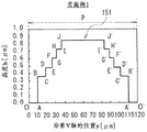
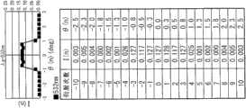
Figure 12 A and Figure 12 B illustrate the structure of the diffraction element 15 of embodiment 1.Particularly, Figure 12 A and Figure 12 B illustrate in each cellular construction 151 (the one dimension diffraction structure that has unit interval P and be made of paired ledge surface structure) of diffraction element 15 by the lip-deep position (along the position y of Y-axis) of each mark (A to J, A ' are to J ', O and O ') expression and the height " h " of these positions.In addition, it is that the condition (B) of green laser Lg of 532nm is lower and be under the condition (C) of blue laser Lb of 445nm at wavelength that Figure 13 A to Figure 13 C illustrates respectively under wavelength is the condition (A) of red laser Lr of 640nm, at wavelength, from the relation between diffraction number of times, intensity I (n) and the angle θ (n) of the diffracted beam of diffraction element 15 outgoing.
From Figure 12 A, Figure 12 B and Figure 13 A to Figure 13 C, can obviously find out, at red laser Lr, green laser Lg and blue laser Lb in each, 0 time, ± 1 time, ± diffracted beam (diffracted beams of 7 number of times) of 2 times and ± 3 times presents the diffraction efficiency (basically more than 10%) far above the diffracted beam of other number of times.From this result, preferably, diffraction element 15 and cellular construction 151 all formed so that generated the diffracted beam (perhaps for the apparent brightness factor of human eye, the diffracted beam of substantially the same brightness) of substantially the same intensity (light quantity) for number of times as much as possible.
Figure 14 is the synoptic diagram of structure that illustrates the interference pattern measuring system of embodiment 2.The measuring system of embodiment 2 comprises green laser 11G, lens 12G, diffraction element 15, drive division 16, fly's-eye lens 17, telecentric optical system (telecentric optical system) 41, rectangular aperture 42, projection lens 23, screen 30 and camera head 43, and camera head 43 has charge-coupled image sensor (CCD) 432 and pick-up lens 431.Note that in these assemblies of this measuring system, comprise that light source portion, drive division 16, aperture 42, projection lens 23, image and the camera head 43 of projection on screen 30 of green laser 11G and lens 12G has following detailed construction.
Detailed construction
Light source portion: wavelength=532nm and diameter
 Green laser beam Lg (parallel beam)
Drive division 16: the amplitude=0.3mm during vibration (along Y-axis), vibration frequency=90Hz
Aperture 42: aspect ratio=16: 9
Projection lens 23:F number=2.0, focal length=5mm
Projected image: 25inch (inch)
Camera head 43: resolution=1392 pixels * 1040 pixels, size=2/3inch, F number=16, focal length=50mm, object distance=933mm
Cs=(σ/I)····(1)
Here, σ represents the standard deviation of Luminance Distribution (or intensity distributions), and I represents the mean value of Luminance Distribution.
Measuring condition
Measure numerical value: luminance level (luminance gradation)
Measured zone 52: the middle section that is defined in the centre of view field 51 along X-axis and Y-axis
Direction of measurement: the both direction along X-axis and Y-axis in the measured zone 52
Figure 16 (A) part and (B) part illustrate the measurement result of the interference pattern of generation comparative example 2 (removed diffraction element 15 and drive division 16 from the measuring system shown in Figure 14 after example).Simultaneously, Figure 16 (C) part and the measurement result that (D) partly illustrates the interference pattern that in embodiment 2, generates.In further detail, Figure 16 (A) part and (C) part and illustrate relation between the intensity (brightness) of pixel quantity (imaging pixels quantity) on the X-axis and the image pickup signal on the X-axis corresponding in the measurement result of direction of measurement under the condition of X-axis.Simultaneously, Figure 16 (B) part and (D) part and illustrate relation between the intensity (brightness) of pixel quantity (imaging pixels quantity) on the Y-axis and the image pickup signal on the Y-axis corresponding in the measurement result of direction of measurement under the condition of Y-axis.Can find out obviously that from (A) part to (D) part of Figure 16 the occurrence degree of the speckle pattern that embodiment 2 (speckle contrast Cs=0.31) presents is lower than the occurrence degree of the speckle pattern of comparative example 2 (speckle contrast Cs=0.46).In other words, can be understood as: the image quality of embodiment 2 is improved.
Three, variation
Then, will the variation (variation 1 is to variation 3) of above-mentioned embodiment be described.Should be noted in the discussion above that with above-mentioned embodiment in identical ingredient be endowed identical Reference numeral and represent, and will suitably omit their description.
In the above-described embodiment, for example shown in the arrow P 2 among Figure 17 A, drive division 16 makes diffraction element 15 (in other words along Y-axis) vibration in the orientation of cellular construction 151.Yet embodiment of the present invention are not limited to this.Particularly, as long as diffraction element 15 has vibration in the direction that contains the orientation component (Y-axis component) of cellular construction 151 with the inherence, plane (X-Y plane) of optical axis Z0 quadrature, diffraction element 15 can vibrate by the modes such as the sort of mode described in the following variation that will illustrate 1.
For example, shown in the arrow P 3 among Figure 17 B, diffraction element 15 can with the plane (X-Y plane) of optical axis Z0 quadrature in for example containing on the vergence direction of orientation component (Y-axis component) of cellular construction 151 (perhaps with X-axis and Y-axis all on the uneven direction) vibration.Scheme as an alternative, for example shown in the arrow P 4 among Figure 17 C, diffraction element 15 can with the plane (X-Y plane) of optical axis Z0 quadrature in vibrate with circular motion, the track of this circular motion contains the orientation component (Y-axis component) of cellular construction 151.
Adopt this kind variation of above-mentioned technology also can realize the function identical with function in above-mentioned embodiment etc., and produced identical effect.In other words, can in the generation (perhaps improving image quality) that reduces interference pattern, realize the utilization ratio of miniaturization and raising light.
Figure 18 is the structure (Y-Z cross section structure) of the optical element (optical element 15-1) that illustrates variation 2 and the synoptic diagram of function.The lighting device of this variation comprises a plurality of optical elements as a concrete and nonrestrictive example of " optical element " in the embodiment of the present invention, and other structure of the lighting device of this variation is identical with the structure of lighting device 1.Note that Figure 18 schematically illustrates the equiphase corrugated of incident beam Lin and outgoing beam Lout1 and outgoing beam Lout2, and follow-up similar accompanying drawing illustrates in a similar fashion.
Optical element 15-1 is such optical system: wherein, a plurality of optical elements are being arranged along optical axis Z0 relative to one another.In this example, along the positive side direction of Z axis and the phase-change element 15A that below optical axis Z0 is furnished with successively, will illustrate and prism array (prism element) 15B.
Phase-change element 15A has such structure: wherein, for example as (A) among Figure 19 the part and (B) part shown in, a plurality of cellular construction 151A along Y-axis be arranged side by side (or arrangement).Each cellular construction 151A has multi-stage surface structure (ledge surface structure or ledge structure), and each is extending these multi-stage surface structures along X-axis in the exit direction (the positive side towards Z axis) of laser beam.In other words, these cellular constructions 151A is being arranged side by side in (along Y-axis) on the following direction: direction (it is along the X-axis) quadrature that this direction and these multiple-rank arrangements extend in light-emitting face (X-Y plane).For example, as shown in Figure 21 A, phase-change element 15A with above-mentioned structure penetrates outgoing beam Lout1 thus by allowing the phase place of the corresponding each several part in the unit area (being formed with a cellular construction 151A in each unit area) with predetermined among the incident beam Lin change independently of each other.
In this variation, drive division 16 for example optionally drives the phase-change element 15A of optical element 15-1 shown in the arrow P 2 among Figure 18.Particularly, by adopting in the technology described in above-mentioned embodiment or the variation 1, make phase-change element 15A with the plane of optical axis Z0 quadrature in (perhaps in X-Y plane on the direction) vibration on the direction.
In the one-piece construction of optical element 15-1, as shown in Figure 18, at first, phase place by the phase-change element 15A each several part that the unit area (being formed with a cellular construction 151A in each unit area) with predetermined of incident beam Lin is corresponding changes independently of each other, and makes outgoing beam Lout1 from phase-change element 15A outgoing.Then, be separated into two light paths from the light path of the outgoing beam Lout1 of phase-change element 15A by prism array 15B, and make outgoing beam Lout2 from prism array 15B outgoing.Therefore, optical element 15-1 has produced the action effect identical with the action effect that is produced by diffraction element illustrated in the above-mentioned embodiment 15 on the whole.
Therefore, this variation also can realize the function identical with function in above-mentioned embodiment etc., and produces identical effect.In other words, can in the generation (perhaps improving image quality) that reduces interference pattern, realize the utilization ratio of miniaturization and raising light.
Figure 22 is the structure (Y-Z cross section structure) of the optical element (optical element 15-2) that illustrates variation 3 and the synoptic diagram of function.Be similar to top variation 2, the lighting device of this variation comprises a plurality of optical elements as a concrete and nonrestrictive example of " optical element " of embodiment of the present invention, and other structure of this variation 3 is identical with structure in the lighting device 1.
Yet in this variation, the liquid crystal cell 15C that will illustrate below the difference of the optical element 15-1 in optical element 15-2 and the variation 2 has been to comprise replaces phase-change element 15A.
In this variation, for example as shown in Figure 22, drive division 16 optionally drives the liquid crystal cell 15C of optical element 15-2.Particularly, drive division 16 applies predetermined driving voltage V to liquid crystal cell 15C accordingly with each cellular construction 151C.By this way, so that the as mentioned above independently of each other change of the phase place of the each several part corresponding with above-mentioned each unit area (being formed with a cellular construction 151C in each unit area) among the incident beam Lin.
In the one-piece construction of optical element 15-2, as shown in Figure 22, at first, allow the phase place of the corresponding each several part in the unit area (being formed with a cellular construction 151C in each unit area) with predetermined among the incident beam Lin change independently of each other by phase-change element 15C, and make outgoing beam Lout1 from liquid crystal cell 15C outgoing.Then, be separated into two light paths from the light path of the outgoing beam Lout1 of liquid crystal cell 15C by prism array 15B, and make outgoing beam Lout2 from prism array 15B outgoing.Therefore, optical element 15-2 has produced the action effect identical with the action effect that is produced by diffraction element illustrated in the above-mentioned embodiment 15 on the whole.
Therefore, this variation also can realize the function identical with function in above-mentioned embodiment etc., and produces identical effect.In other words, can in the generation (perhaps improving image quality) that reduces interference pattern, realize the utilization ratio of miniaturization and raising light.
Other variation
So far, this paper is by having illustrated as an example technology of the present invention with embodiment, each embodiment and each variation, yet technology of the present invention is not limited to above-mentioned embodiment etc., and can make various modifications.
For example, as the example of " optical element " of embodiment of the present invention, above-mentioned embodiment etc. have illustrated the combination of diffraction element, phase-change element and prism array and these three kinds of situations of combination of liquid crystal cell and prism array.Yet, also can use any element except these examples.In addition, as " optics " of embodiment of the present invention, can use any optics (for example, bar-shaped integrator etc.) except the fly's-eye lens that in above-mentioned embodiment etc., has illustrated.
In above-mentioned embodiment etc., the situation that has illustrated be various light sources (red light source, green light source and blue-light source) each be LASER Light Source, but embodiments of the present invention are not limited to this situation.Scheme as an alternative, at least a in the described various light sources can be LASER Light Source.The combination of LASER Light Source and other light source except LASER Light Source (such as led light source etc.) can be set in light source portion particularly.
In above-mentioned embodiment etc., illustrated that wherein the example of optical modulation element is the situation of reflection type optical modulator element, yet, the invention is not restricted to this.Scheme for example, can replace the reflection type optical modulator element with the transmission-type liquid crystal element as an alternative.In addition, can use any optical modulation element except liquid crystal cell.
In above-mentioned embodiment etc., the situation that has illustrated is to have used three kinds of light sources that send the different wave length bundle, still, for example not only can use three kinds of light sources, also can use a kind of, two kinds, four kinds or more kinds of light source.
Above-mentioned embodiments etc. have illustrated concrete (optics) member in lighting device and the display device.But, be not to be provided with whole above-mentioned members, and can also add any other member.Particularly, dichronic mirror for example can be set and replace dichroic prism 131 and dichroic prism 132.
In above-mentioned embodiment etc., the situation that has illustrated is: display device is equipped with for the projection optical system (projection lens) that the light of being modulated by above-mentioned optical modulation element is projected on the screen, and this display device is configured to projection display equipment.But technology of the present invention for example also goes for direct viewing type (direct-view) display device.
Therefore, can obtain following technical scheme at least from above-mentioned exemplary of the present invention and each variation.
1. a kind of lighting device, described lighting device comprises:
Light source portion, described light source portion comprises LASER Light Source;
Optical element, described optical element is arranged on the light path of the laser beam that sends from described LASER Light Source, described optical element is separated into a plurality of light paths to the light path that is incident to the incident beam on the described optical element, and makes light beam after the separation from described optical element outgoing;
Optics, described optics receive the light beam after the described separation of propagating along described a plurality of light paths, and based on the light beam after the described separation from described optics outgoing illumination light; And
Drive division, described drive division drives described optical element, so that the phase place of the light beam after the described separation changes independently of each other.
2. according to 1. described lighting device, wherein said optical element comprises diffraction element, is arranged with a plurality of predetermined cellular constructions in described diffraction element.
3. according to 2. described lighting device, wherein said drive division make described diffraction element with the optical axis of described diffraction element basically in the plane of quadrature direction vibrate, thus so that consist of the phase place of each time diffracted beam of the light beam after the described separation and change independently of each other.
4. according to 3. described lighting device, wherein said drive division makes described diffraction element basically vibrate in the direction of the orientation component that contains described cellular construction in the plane of quadrature with described optical axis.
5. according to 4. described lighting device, wherein said drive division makes described diffraction element vibrate in the orientation of described cellular construction.
6. according to 2. to 5. any one described lighting device, wherein
Each described cellular construction includes a pair of multistage surface structure, and described a pair of multistage surface structure is symmetrical about the predetermined plane of the normal that comprises diffraction surfaces, and
Described a pair of multistage surface structure is arranged on the described diffraction surfaces with one dimension mode or two-dimensional approach.
7. according to 1. described lighting device, wherein
Described optical element comprises phase-change element and prism array, and described phase-change element and described prism array arranging along optical axis separately in mode respect to one another,
Described phase-change element changes the phase place of the each several part corresponding with each predetermined unit area of described incident beam independently of each other, and makes light beam after phase place changes from described phase-change element outgoing,
The light path of the light beam after described prism array changes the described phase place from described phase-change element outgoing is separated into described a plurality of light path, and makes light beam after the described separation from described prism array outgoing, and
Described drive division drives described phase-change element.
8. according to 7. described lighting device, wherein said drive division make described phase-change element with the optical axis of described phase-change element basically in the plane of quadrature direction vibrate.
9. according to 7. described lighting device, wherein
Described phase-change element comprises the liquid crystal cell with predetermined cellular construction, and described predetermined cellular construction forms corresponding to each described unit area, and
Described drive division and each described cellular construction apply predetermined driving voltage to described liquid crystal cell accordingly.
10. according to 1. to 9. any one described lighting device, wherein said optics comprises fly's-eye lens.


A kind of display device, described display device has lighting device and optical modulation element, and described optical modulation element is modulated the illumination light that obtains from described lighting device based on picture signal, and described lighting device is as 1. extremely
 In any one described lighting device.


It will be appreciated by those skilled in the art that according to designing requirement and other factors, can in the scope of claim that the present invention encloses or its equivalent, carry out various modifications, combination, inferior combination and change.
Claims (15)
1. lighting device, described lighting device comprises:
Light source portion, described light source portion comprises LASER Light Source;
Optical element, described optical element is arranged on the light path of the laser beam that sends from described LASER Light Source, described optical element is separated into a plurality of light paths to the light path that is incident to the incident beam on the described optical element, and makes light beam after the separation from described optical element outgoing;
Optics, described optics receive the light beam after the described separation of propagating along described a plurality of light paths, and based on the light beam after the described separation from described optics outgoing illumination light; And
Drive division, described drive division drives described optical element, so that the phase place of the light beam after the described separation changes independently of each other.
2. lighting device according to claim 1 is characterized in that, described optical element comprises diffraction element, is arranged with a plurality of predetermined cellular constructions in described diffraction element.
3. lighting device according to claim 2, it is characterized in that, described drive division make described diffraction element with the optical axis of described diffraction element basically in the plane of quadrature direction vibrate, thus so that consist of the phase place of each time diffracted beam of the light beam after the described separation and change independently of each other.
4. lighting device according to claim 3 is characterized in that, described drive division makes described diffraction element basically vibrate in the direction of the orientation component that contains described cellular construction in the described plane of quadrature with described optical axis.
5. lighting device according to claim 4 is characterized in that, described drive division makes described diffraction element vibrate in the orientation of described cellular construction.
6. lighting device according to claim 2 is characterized in that,
Each described cellular construction includes a pair of multistage surface structure, and described a pair of multistage surface structure is symmetrical about the predetermined plane of the normal that comprises diffraction surfaces, and
Described a pair of multistage surface structure is arranged on the described diffraction surfaces with one dimension mode or two-dimensional approach.
7. lighting device according to claim 1 is characterized in that,
Described optical element comprises phase-change element and prism array, and described phase-change element and described prism array arranging along optical axis separately in mode respect to one another,
Described phase-change element changes the phase place of the each several part corresponding with each predetermined unit area of described incident beam independently of each other, and makes light beam after phase place changes from described phase-change element outgoing,
The light path of the light beam after described prism array changes the described phase place from described phase-change element outgoing is separated into described a plurality of light path, and makes light beam after the described separation from described prism array outgoing, and
Described drive division drives described phase-change element.
8. lighting device according to claim 7 is characterized in that, described drive division make described phase-change element with the optical axis of described phase-change element basically in the plane of quadrature direction vibrate.
9. lighting device according to claim 7 is characterized in that,
Described phase-change element comprises the liquid crystal cell with predetermined cellular construction, and described predetermined cellular construction forms corresponding to each described unit area, and
Described drive division and each described cellular construction apply predetermined driving voltage to described liquid crystal cell accordingly.
10. each described lighting device in 9 according to claim 1 is characterized in that described optics comprises fly's-eye lens.
11. each described lighting device in 9 is characterized in that described light source portion comprises three kinds of light sources that send respectively red beam, green beam and blue light beam according to claim 1.
12. lighting device according to claim 11 is characterized in that, at least a in described three kinds of light sources is LASER Light Source.
13. display device, described display device has lighting device and optical modulation element, described optical modulation element is modulated the illumination light that obtains from described lighting device based on picture signal, and described lighting device is such as each described lighting device in the claim 1 to 12.
14. display device according to claim 13 also comprises projection optical system, described projection optical system is being projected on the projecting plane by the described illumination light after the described optical modulation element modulation.
15. display device according to claim 13 is characterized in that, described optical modulation element comprises liquid crystal cell.
Applications Claiming Priority (2)
| Application Number | Priority Date | Filing Date | Title |
|---|---|---|---|
| JP2011180779A JP2013044800A (en) | 2011-08-22 | 2011-08-22 | Illumination device and display device |
| JP2011-180779 | 2011-08-22 |
Publications (1)
| Publication Number | Publication Date |
|---|---|
| CN102955343A true CN102955343A (en) | 2013-03-06 |
Family
ID=47743043
Family Applications (1)
| Application Number | Title | Priority Date | Filing Date |
|---|---|---|---|
| CN2012102809702A Pending CN102955343A (en) | 2011-08-22 | 2012-08-08 | Illumination device and display device |
Country Status (3)
| Country | Link |
|---|---|
| US (1) | US20130050285A1 (en) |
| JP (1) | JP2013044800A (en) |
| CN (1) | CN102955343A (en) |
Cited By (7)
| Publication number | Priority date | Publication date | Assignee | Title |
|---|---|---|---|---|
| CN104808425A (en) * | 2014-01-26 | 2015-07-29 | 中能激光显示技术(上海)有限公司 | Laser light source light beam parameter consistency adjusting device and adjusting method thereof |
| CN105404089A (en) * | 2014-09-05 | 2016-03-16 | 威视恩移动有限公司 | Suspending cover which improves and eliminates double reflections and panorama optical device thereof |
| CN107533238A (en) * | 2015-04-30 | 2018-01-02 | Sk电信有限公司 | Speckle reduction means |
| CN110873997A (en) * | 2018-08-29 | 2020-03-10 | Jvc建伍株式会社 | Projection type image display apparatus |
| CN112955790A (en) * | 2018-08-31 | 2021-06-11 | 陈从亮 | Microscope with LED illumination assembly |
| CN113039484A (en) * | 2018-11-13 | 2021-06-25 | 索尼集团公司 | Image display device |
| CN113670852A (en) * | 2016-05-13 | 2021-11-19 | 苏州高迎检测技术有限公司 | Inspection apparatus and inspection method |
Families Citing this family (9)
| Publication number | Priority date | Publication date | Assignee | Title |
|---|---|---|---|---|
| JP6160144B2 (en) * | 2013-03-15 | 2017-07-12 | セイコーエプソン株式会社 | Lighting device and projector |
| JP6237107B2 (en) * | 2013-10-21 | 2017-11-29 | セイコーエプソン株式会社 | projector |
| JP6287355B2 (en) * | 2014-03-05 | 2018-03-07 | セイコーエプソン株式会社 | projector |
| KR20150115082A (en) | 2014-04-02 | 2015-10-14 | 삼성디스플레이 주식회사 | Backlight unit and display divece having the same |
| JP6815715B2 (en) * | 2014-08-29 | 2021-01-20 | 日亜化学工業株式会社 | Light source device and projector equipped with the light source device |
| KR101587788B1 (en) * | 2015-02-13 | 2016-01-22 | 주식회사 크레모텍 | Liquid crystal projector using laser diode |
| CA3074566A1 (en) * | 2017-08-31 | 2019-03-07 | Metalenz, Inc. | Transmissive metasurface lens integration |
| JP6696629B1 (en) | 2018-10-22 | 2020-05-20 | 三菱電機株式会社 | Laser equipment |
| US11927769B2 (en) | 2022-03-31 | 2024-03-12 | Metalenz, Inc. | Polarization sorting metasurface microlens array device |
Citations (8)
| Publication number | Priority date | Publication date | Assignee | Title |
|---|---|---|---|---|
| US6064452A (en) * | 1996-04-17 | 2000-05-16 | Hitachi, Ltd. | Single plate color liquid crystal display apparatus |
| JP2000206449A (en) * | 1999-01-18 | 2000-07-28 | Sony Corp | Illuminator, illuminating method and image display device |
| US20030039036A1 (en) * | 2001-08-27 | 2003-02-27 | Eastman Kodak Company | Laser projection display system |
| US20090033814A1 (en) * | 2007-08-01 | 2009-02-05 | Sajjad Ali Khan | Method and apparatus for reducing speckle in coherent light |
| US20090185141A1 (en) * | 2008-01-22 | 2009-07-23 | Lucent Technologies, Inc. | Diffuser configuration for an image projector |
| CN101661214A (en) * | 2008-08-27 | 2010-03-03 | 鸿富锦精密工业(深圳)有限公司 | Projector |
| US20100220299A1 (en) * | 2006-05-26 | 2010-09-02 | Tetsuro Mizushima | Image display device |
| US20110043768A1 (en) * | 2009-04-10 | 2011-02-24 | Kenji Nakayama | Image display apparatus |
Family Cites Families (1)
| Publication number | Priority date | Publication date | Assignee | Title |
|---|---|---|---|---|
| JP4497212B2 (en) * | 2008-02-20 | 2010-07-07 | ソニー株式会社 | Light source system |
-
2011
- 2011-08-22 JP JP2011180779A patent/JP2013044800A/en not_active Abandoned
-
2012
- 2012-08-01 US US13/564,096 patent/US20130050285A1/en not_active Abandoned
- 2012-08-08 CN CN2012102809702A patent/CN102955343A/en active Pending
Patent Citations (8)
| Publication number | Priority date | Publication date | Assignee | Title |
|---|---|---|---|---|
| US6064452A (en) * | 1996-04-17 | 2000-05-16 | Hitachi, Ltd. | Single plate color liquid crystal display apparatus |
| JP2000206449A (en) * | 1999-01-18 | 2000-07-28 | Sony Corp | Illuminator, illuminating method and image display device |
| US20030039036A1 (en) * | 2001-08-27 | 2003-02-27 | Eastman Kodak Company | Laser projection display system |
| US20100220299A1 (en) * | 2006-05-26 | 2010-09-02 | Tetsuro Mizushima | Image display device |
| US20090033814A1 (en) * | 2007-08-01 | 2009-02-05 | Sajjad Ali Khan | Method and apparatus for reducing speckle in coherent light |
| US20090185141A1 (en) * | 2008-01-22 | 2009-07-23 | Lucent Technologies, Inc. | Diffuser configuration for an image projector |
| CN101661214A (en) * | 2008-08-27 | 2010-03-03 | 鸿富锦精密工业(深圳)有限公司 | Projector |
| US20110043768A1 (en) * | 2009-04-10 | 2011-02-24 | Kenji Nakayama | Image display apparatus |
Cited By (9)
| Publication number | Priority date | Publication date | Assignee | Title |
|---|---|---|---|---|
| CN104808425A (en) * | 2014-01-26 | 2015-07-29 | 中能激光显示技术(上海)有限公司 | Laser light source light beam parameter consistency adjusting device and adjusting method thereof |
| CN105404089A (en) * | 2014-09-05 | 2016-03-16 | 威视恩移动有限公司 | Suspending cover which improves and eliminates double reflections and panorama optical device thereof |
| CN107533238A (en) * | 2015-04-30 | 2018-01-02 | Sk电信有限公司 | Speckle reduction means |
| CN113670852A (en) * | 2016-05-13 | 2021-11-19 | 苏州高迎检测技术有限公司 | Inspection apparatus and inspection method |
| CN110873997A (en) * | 2018-08-29 | 2020-03-10 | Jvc建伍株式会社 | Projection type image display apparatus |
| CN110873997B (en) * | 2018-08-29 | 2022-04-05 | Jvc建伍株式会社 | Projection type image display apparatus |
| CN112955790A (en) * | 2018-08-31 | 2021-06-11 | 陈从亮 | Microscope with LED illumination assembly |
| CN113039484A (en) * | 2018-11-13 | 2021-06-25 | 索尼集团公司 | Image display device |
| CN113039484B (en) * | 2018-11-13 | 2023-04-28 | 索尼集团公司 | Image display device |
Also Published As
| Publication number | Publication date |
|---|---|
| US20130050285A1 (en) | 2013-02-28 |
| JP2013044800A (en) | 2013-03-04 |
Similar Documents
| Publication | Publication Date | Title |
|---|---|---|
| CN102955343A (en) | Illumination device and display device | |
| JP5682813B2 (en) | Lighting device and projector | |
| JP5195991B2 (en) | Illumination device and display device | |
| CN102879988B (en) | Lighting device and display device | |
| JP5090900B2 (en) | Two-dimensional image forming apparatus | |
| JP4301282B2 (en) | projector | |
| US20120154767A1 (en) | Light source apparatus | |
| KR100828367B1 (en) | Laser displasy apparatus | |
| JP2004151133A (en) | Optical device of illumination in image display and image display | |
| JP2010510643A (en) | Visual display lighting system | |
| JP2012032585A (en) | Projector | |
| CN103376636A (en) | Display unit and illumination device | |
| JP2014092663A (en) | Polarization demultiplexing/multiplexing element, optical system, and display device | |
| CN102734700A (en) | Illumination device and display unit | |
| US6619801B2 (en) | Projection type image display apparatus realizing three-dimensional image | |
| JP2012079622A (en) | Light source device and projector | |
| US9175826B2 (en) | Illuminating unit and display | |
| JP2011154930A (en) | Lighting device and projector | |
| JP5991389B2 (en) | Lighting device and projector | |
| JP2014048377A (en) | Display device and lighting device | |
| JP2021051171A (en) | projector | |
| JP6323072B2 (en) | Lighting device and projector | |
| JP2012163582A (en) | Projector | |
| US10845578B2 (en) | Light source device and projection display apparatus | |
| JP5500235B2 (en) | Illumination device and display device |
Legal Events
| Date | Code | Title | Description |
|---|---|---|---|
| C06 | Publication | ||
| PB01 | Publication | ||
| C10 | Entry into substantive examination | ||
| SE01 | Entry into force of request for substantive examination | ||
| C02 | Deemed withdrawal of patent application after publication (patent law 2001) | ||
| WD01 | Invention patent application deemed withdrawn after publication |
Application publication date: 20130306 |