CN102348052B - Electronic apparatus - Google Patents
Electronic apparatus Download PDFInfo
- Publication number
- CN102348052B CN102348052B CN201110212321.4A CN201110212321A CN102348052B CN 102348052 B CN102348052 B CN 102348052B CN 201110212321 A CN201110212321 A CN 201110212321A CN 102348052 B CN102348052 B CN 102348052B
- Authority
- CN
- China
- Prior art keywords
- connector
- transmission lines
- difference transmission
- area
- terminal
- Prior art date
- Legal status (The legal status is an assumption and is not a legal conclusion. Google has not performed a legal analysis and makes no representation as to the accuracy of the status listed.)
- Active
Links
Images


Classifications
-
- H—ELECTRICITY
- H05—ELECTRIC TECHNIQUES NOT OTHERWISE PROVIDED FOR
- H05K—PRINTED CIRCUITS; CASINGS OR CONSTRUCTIONAL DETAILS OF ELECTRIC APPARATUS; MANUFACTURE OF ASSEMBLAGES OF ELECTRICAL COMPONENTS
- H05K1/00—Printed circuits
- H05K1/02—Details
- H05K1/0213—Electrical arrangements not otherwise provided for
- H05K1/0216—Reduction of cross-talk, noise or electromagnetic interference
- H05K1/0218—Reduction of cross-talk, noise or electromagnetic interference by printed shielding conductors, ground planes or power plane
- H05K1/0219—Printed shielding conductors for shielding around or between signal conductors, e.g. coplanar or coaxial printed shielding conductors
-
- H—ELECTRICITY
- H05—ELECTRIC TECHNIQUES NOT OTHERWISE PROVIDED FOR
- H05K—PRINTED CIRCUITS; CASINGS OR CONSTRUCTIONAL DETAILS OF ELECTRIC APPARATUS; MANUFACTURE OF ASSEMBLAGES OF ELECTRICAL COMPONENTS
- H05K1/00—Printed circuits
- H05K1/02—Details
- H05K1/11—Printed elements for providing electric connections to or between printed circuits
- H05K1/118—Printed elements for providing electric connections to or between printed circuits specially for flexible printed circuits, e.g. using folded portions
-
- H—ELECTRICITY
- H05—ELECTRIC TECHNIQUES NOT OTHERWISE PROVIDED FOR
- H05K—PRINTED CIRCUITS; CASINGS OR CONSTRUCTIONAL DETAILS OF ELECTRIC APPARATUS; MANUFACTURE OF ASSEMBLAGES OF ELECTRICAL COMPONENTS
- H05K1/00—Printed circuits
- H05K1/02—Details
- H05K1/0213—Electrical arrangements not otherwise provided for
- H05K1/0237—High frequency adaptations
- H05K1/0245—Lay-out of balanced signal pairs, e.g. differential lines or twisted lines
-
- H—ELECTRICITY
- H05—ELECTRIC TECHNIQUES NOT OTHERWISE PROVIDED FOR
- H05K—PRINTED CIRCUITS; CASINGS OR CONSTRUCTIONAL DETAILS OF ELECTRIC APPARATUS; MANUFACTURE OF ASSEMBLAGES OF ELECTRICAL COMPONENTS
- H05K1/00—Printed circuits
- H05K1/02—Details
- H05K1/14—Structural association of two or more printed circuits
- H05K1/147—Structural association of two or more printed circuits at least one of the printed circuits being bent or folded, e.g. by using a flexible printed circuit
-
- H—ELECTRICITY
- H05—ELECTRIC TECHNIQUES NOT OTHERWISE PROVIDED FOR
- H05K—PRINTED CIRCUITS; CASINGS OR CONSTRUCTIONAL DETAILS OF ELECTRIC APPARATUS; MANUFACTURE OF ASSEMBLAGES OF ELECTRICAL COMPONENTS
- H05K2201/00—Indexing scheme relating to printed circuits covered by H05K1/00
- H05K2201/09—Shape and layout
- H05K2201/09209—Shape and layout details of conductors
- H05K2201/09654—Shape and layout details of conductors covering at least two types of conductors provided for in H05K2201/09218 - H05K2201/095
- H05K2201/097—Alternating conductors, e.g. alternating different shaped pads, twisted pairs; Alternating components
-
- H—ELECTRICITY
- H05—ELECTRIC TECHNIQUES NOT OTHERWISE PROVIDED FOR
- H05K—PRINTED CIRCUITS; CASINGS OR CONSTRUCTIONAL DETAILS OF ELECTRIC APPARATUS; MANUFACTURE OF ASSEMBLAGES OF ELECTRICAL COMPONENTS
- H05K2201/00—Indexing scheme relating to printed circuits covered by H05K1/00
- H05K2201/10—Details of components or other objects attached to or integrated in a printed circuit board
- H05K2201/10007—Types of components
- H05K2201/10189—Non-printed connector
Abstract
An electronic apparatus includes a first wiring board formed having a first area, a second area, and a third area, wherein the first area is formed extending in a first direction from the third area, and the second area is formed extending in a second direction, which is opposite to the first direction, from the third area; a second wiring board connected to the first wiring board; a first connector for connection to an external device, wherein the first connector is mounted on the first area of the first wiring board; a second connector for connection to an external device, wherein the second connector is mounted on the second area of the first wiring board; and a third connector connected to the second wiring board, wherein the third connector is mounted on the third area of the first wiring board, and is formed with a first terminal array and a second terminal array facing each other, wherein on the first wiring board a first differential transmission line is formed in a region from the first connector to the first terminal array, and a second differential transmission line is formed in a region from the second connector to the second terminal array.
Description
Technical field
The present invention relates to a kind of electronic equipment, especially, relate to a kind of electronic equipment that many difference transmission lines is installed on to a wiring plate.
Background technology
In electronic equipments such as digital camera, the frequency of digital signal used increases year by year.In addition, signal transmission rate is also increasing.For signal transmission at high speed, the differential transfer that can to use in recent years by Low Voltage Differential Signal (LVDS) be representative.LVDS is the input/output signal level specification (signallevel specification) that realizes high-speed transfer more than hundreds of M byte per second under the state in order to be reduced to hundreds of mV at amplitude, and this specification is not subject to owing to carrying out the impact of the noise of differential transfer generation via impedance Control wiring.
In addition, in the electronic equipment such as such as digital camera, can use the interface and the communication with external apparatus that adopt differential transfer such as USB (USB) or HDMI (High Definition Multimedia Interface) (HDMI) etc.In this case, in order to increase USB connector in electronic equipment or the installation degree of freedom of HDMI connector, interface can be installed in the printed wiring board different from the printed wiring board that system integrated chip (IC) is installed.TOHKEMY 2007-166290 communique has been discussed via signal connecting connector the signal of USB or HDMI has been connected with the printed wiring board that system IC is installed.
In the time being installed on a printed wiring board as multiple interfaces of the employing such as USB and HDMI differential transfer, utilize the difference transmission lines of different impedance Control to be installed in a printed wiring board.In this case, must prevent crosstalking between difference transmission lines.
Summary of the invention
According to aspects of the present invention, a kind of electronic equipment, it comprises: the first wiring plate, it is formed as having first area, second area and the 3rd region, wherein said first area is formed as extending along first direction from described the 3rd region, and described second area is formed as extending along the second direction contrary with described first direction from described the 3rd region; The second wiring plate, it is connected to described the first wiring plate; The first connector, it is for being connected to external device (ED), and wherein said the first connector is installed in the described first area of described the first wiring plate; The second connector, it is for being connected to external device (ED), and wherein said the second connector is installed in the described second area of described the first wiring plate; And the 3rd connector, it is connected to described the second wiring plate, wherein said the 3rd connector is installed in described the 3rd region of described the first wiring plate, and described the 3rd connector is formed with the first terminal row and the second terminal row that face with each other, wherein, on described the first wiring plate, the first difference transmission lines is formed on the scope from described the first connector to described the first terminal row, and the second difference transmission lines is formed on the scope from described the second connector to described the second terminal row.
According to the present invention, even in the time utilizing the difference transmission lines of different impedance Control to be installed in a printed wiring board, still can reduce crosstalking and can prevent impedance mismatching between difference transmission lines.
From the detailed description to illustrative embodiments with reference to the accompanying drawings, it is obvious that further feature of the present invention and aspect will become.
Accompanying drawing explanation
The accompanying drawing that is contained in specification and form a part for specification illustrates illustrative embodiments of the present invention, feature and aspect, and is used from and explains principle of the present invention with explanation one.
Figure 1A and Figure 1B are the stereoscopic figure as digital camera according to an illustrative embodiment of the invention.
Fig. 2 is the expanded view as the printed wiring board of the first wiring plate.
(A) of Fig. 3 and (B) be the wiring pattern figure as the printed wiring board of the first wiring plate.
Fig. 4 is the enlarged drawing in the region that USB connector is installed of printed wiring board.
Fig. 5 is the enlarged drawing in the region that HDMI connector is installed of printed wiring board.
Fig. 6 is the enlarged drawing that the part of (board-to board) connector between plate is installed of printed wiring board.
Fig. 7 A to Fig. 7 D illustrates the process for printed wiring board being installed to camera body.
Fig. 8 A to Fig. 8 C is the stereogram illustrating while using external interface.
Embodiment
Describe below with reference to accompanying drawings various illustrative embodiments of the present invention, feature and aspect in detail.
Figure 1A and Figure 1B are as according to the stereoscopic figure of the digital camera of the example of the electronic equipment of this illustrative embodiments.Digital camera has camera body 1, protecgulum 2, bonnet 3, top base 4, lens barrel (lens barrel) unit 5 and is arranged in the socket lid 6 of camera body side.Socket lid 6 is supported with respect to camera body 1 in the mode that can open and close.Be configured in the inner side of socket lid 6 below for the external interface of communicating by letter with described external device data.In this illustrative embodiments, USB connector and HDMI connector are configured to external interface.By insert these connectors respectively special cable can make digital camera be connected with external equipment.
Then,, by utilizing Fig. 2 that the printed wiring board 10 as the first wiring plate according to this illustrative embodiments is described, be wherein installed in the first wiring plate as the USB connector 11 of the first connector with as the HDMI connector 12 of the second connector.Flexible flexible printing wiring board according to the printed wiring board 10 of this illustrative embodiments.USB connector 11 and HDMI connector 12 are installed in same flexible printing wiring board 10 (hereinafter, " socket flexible board 10 ").There is engagement member and be installed in socket flexible board 10 as the mother daughter board connector 13 of the 3rd connector.As described below, mother daughter board connector 13 is set to be electrically connected with the printed wiring board 40 as the second wiring plate, and wherein system IC is installed in printed wiring board 40.More specifically, by the mother daughter board connector 13 as the 3rd connector, can be electrically connected with the printed wiring board 40 as the second wiring plate as the socket flexible board 10 of the first wiring plate.Mother daughter board connector 13 has the first terminal row 14 and the second terminal row 15 with the contact portion of socket flexible board 10, and wherein the first terminal row 14 are with preset space length configuration, and the second terminal row 15 are configured in the face of the first terminal row 14 with preset space length.
Socket flexible board 10 by be provided with USB connector 11 first area A, the second area B of HDMI connector 12 is installed and be positioned at first area and second area between the 3rd region C form.First area is formed as extending along first direction 16 from the 3rd region.Second area is formed as extending along the second direction 17 contrary with first direction from the 3rd region.Be positioned at mode that the first area side of socket flexible board 10 and the second terminal row 15 of mother daughter board connector 13 are positioned at the second area side of socket flexible board 10 mother daughter board connector 13 be installed on the 3rd region of socket flexible board 10 with the first terminal row 14 of mother daughter board connector 13.
Particularly, as shown in Figure 2, mother daughter board connector 13 is installed in the mode in the 3rd region of crosscut socket flexible board 10.Socket flexible board 10 has the shape of extending along first direction 16 from the first terminal row 14 of mother daughter board connector 13 and the shape of extending along second direction 17 from the second terminal row 15.In addition, socket flexible board 10 is connected with the second area that HDMI connector 12 is installed with the first area that USB connector 11 is installed via the angular shape that is roughly " L " shape.
Be formed on first area from USB connector 11 is installed to the scope of the first terminal row 14 of mother daughter board connector 13 as the difference transmission lines 20 of the first difference transmission lines.Be formed on second area from HDMI connector 12 is installed to the scope of the second terminal row 15 of mother daughter board connector 13 as the difference transmission lines 24a to 24d of the second difference transmission lines.Therefore, difference transmission lines 20 forms along first direction 16 from the first terminal row 14 of mother daughter board connector 13, and difference transmission lines 24a to 24d forms along second direction 17 from the second terminal row 15 of mother daughter board connector 13.
Then, (A) of Fig. 3 and (B) wiring pattern of explanation socket flexible board 10 will be utilized.(A) of Fig. 3 illustrates the wiring pattern of parts installed surface.(B) of Fig. 3 illustrates the wiring pattern of the face contrary with parts installed surface.
First, usb signal wiring pattern will be described.Fig. 4 is the enlarged drawing of the first area A that USB connector 11 is installed of socket flexible board 10.Usb signal wiring pattern has one group of difference transmission lines 20 at parts installed surface.This group difference transmission lines 20 is grounded pattern 21 and protects in both sides.The overlapping region of projection with difference transmission lines 20 and grounding pattern 21 at the back side of USB connector installed surface is grounded pattern 22 and protects.By at wiring right both sides and back-protective difference transmission lines, maintain limited impedance.Usb signal difference transmission lines 20 in this illustrative embodiments is adjusted to 90 Ω.The difference transmission lines being connected up from USB connector portion of terminal 23 is connected to the first terminal row 14 of mother daughter board connector 13 not through through hole.Owing in through hole, impedance mismatching can occurring, so through hole is not preferably set on differential transfer thread path.In this illustrative embodiments, because USB connector 11 and mother daughter board connector 13 are installed in the same face, so can realize wiring without through hole is set for usb signal difference transmission lines in the situation that.
Then, HDMI signal routing pattern will be described.Fig. 5 is the enlarged drawing of the second area B that HDMI connector 12 is installed of socket flexible board 10.HDMI signal routing pattern has four groups of difference transmission lines 24a to 24d at parts installed surface.These difference transmission lines groups 24a to 24d is grounded pattern 25 and protects in both sides.The overlapping region of projection with difference transmission lines 24a to 24d and grounding pattern 25 at the back side of HDMI connector installed surface is grounded pattern 26 and protects.HDMI signal differential transmission line in this illustrative embodiments is adjusted to 100 Ω.HDMI connector 12 and mother daughter board connector 13 are installed in the same face, make the difference transmission lines being connected up from HDMI bonder terminal portion 27 not through through hole, be connected to the second terminal row 15 of mother daughter board connector 13.
Socket flexible board 10 in this illustrative embodiments has the roughly bight of L shaped shape between the second terminal row 15 of HDMI bonder terminal portion 27 and mother daughter board connector.In this illustrative embodiments, by making plate outward appearance be roughly " L " shape, between described and main body installation period, USB connector 11 and HDMI connector 12 can be configured in contiguous position in the back.If difference transmission lines is routed to roughly the bight of " L " shape, be routed at angular shape inner side difference transmission lines 24a and be routed between the difference transmission lines 24d in outside of angular shape and may exist large length of arrangement wire poor.Preferably, each have equal length of arrangement wire to difference transmission lines.Therefore, in this illustrative embodiments, if be routed at the outermost difference transmission lines 24d in bight and be connected to the second terminal row 15 of HDMI bonder terminal portion 27 and mother daughter board connector, with shortest path routing difference transmission lines 24d.Can use this socket flexible board 10 by make 10 bendings of socket flexible board during the socket flexible board 10 in this illustrative embodiments is installed to camera body.Therefore, preferably, the external width of flexible board is as much as possible little.Thus, the terminal pitch that the wire distribution distance of difference transmission lines 24a to 24d is set as to be less than the terminal pitch of HDMI connector 12 and is less than mother daughter board connector 13.Therefore, if connected up to being formed at the outermost difference transmission lines 24d of angular shape with shortest path like that as in this exemplary embodiment, for other difference transmission lines, difference transmission lines, the closer to the inner side of angular shape, just makes this difference transmission lines have more roundabout amounts (detour).Thus, by difference transmission lines being connected up in the difference transmission lines mode that this difference transmission lines has more roundabout amounts the closer to the inner side of angular shape, can improve each difference transmission lines because the bight of " L " shape roughly has the problem of various wirings length.
Conventionally, in the time using mother daughter board connector, usually make to be positioned at respect to wiring direction the wiring that the terminal in the distally of connector uses roundabout to avoid nearside terminal, or at the back side of connector, the wiring that is positioned at the terminal in the distally of connector with respect to wiring direction and uses is connected up, and near of distally terminal, through hole is set.In the time that difference transmission lines is routed to such printed wiring board, difference transmission lines is routed to the terminal of the nearside of mother daughter board connector, and remaining holding wire is routed to the terminal in distally.But if there is like that as in this exemplary embodiment polytype difference transmission lines, difference transmission lines and grounding pattern may not can be all assemblied in the terminal row of a side of mother daughter board connector.Under these circumstances, need to make difference transmission lines roundabout at same a connector face, or difference transmission lines need to be routed to the dorsal part of terminal row, then route to the terminal in distally via through hole.As mentioned above, if because difference transmission lines is routed to the back side of bonder terminal portion, may be owing to the interference of the pattern of bonder terminal portion, impedance mismatching occurring, so preferably do not make difference transmission lines pass through hole.In this illustrative embodiments, for the difference transmission lines of two types, usb signal difference transmission lines 21 connects up along first direction 16 from the first terminal row 14 of mother daughter board connector 13, and HDMI signal differential transmission line 24a to 24d connects up along second direction 17 from the second terminal row 15.Therefore,, even if many difference transmission lines are formed at same plate, also can in mother daughter board connector terminal row, prevent signal interference and impedance mismatching.In addition, by bending the socket flexible board 10 of structure like this and this socket flexible board 10 being disposed to camera body 1, and USB connector 11 and HDMI connector 12 can be disposed to the same face.
Then, explanation is provided with to the configuration pattern of the part of mother daughter board connector 13.Fig. 6 is the enlarged drawing that the 3rd region C of the mother daughter board connector 13 shown in (A) of Fig. 3 is installed.As shown in Figure 6, in mother daughter board connector 13, the terminal being connected with difference transmission lines 24a to 24d in the terminal being connected with difference transmission lines 20 and the second terminal row 15 in the first terminal row 14 is configured to not face each other.Particularly, the terminal being connected with grounding pattern 25 in the terminal being connected with difference transmission lines 20 and the second terminal row 15 in the first terminal row 14 is connected up as facing with each other.Depend on mother daughter board connector, between the first terminal row 14 and the second terminal row 15, may have little gap.Even under these circumstances, by make the terminals faced mutually of terminals that connect for difference transmission lines in the second terminal row 15 and in the first terminal row 14 be grounding pattern or with difference transmission lines different holding wire, the interference between differential signal can be prevented, stable transmission can be realized thus.
Then, explanation is used for socket flexible board 10 to be installed to the process of camera body 1.In Fig. 7 A, the pedestal 30 that is disposed at the upper surface of camera body has the box-shaped portion 31 that is formed as mating with the profile of HDMI connector 12 profile that supports HDMI connector.At the upper surface of pedestal, the frame 33 being formed by hardware is fixed to pedestal 30 by hot melt portion (heat stake) 34.
Then, in stationary state in the situation that, in the ventricumbent mode of installation of HDMI connector 12, socket flexible board 10 is installed to the box-shaped portion 31 (with reference to Fig. 7 B) of pedestal in pedestal 30 and frame 33.Utilize screw 50 that socket flexible board 10 is fixed to frame 33, then the mother daughter board connector of the mother daughter board connector of mainboard 40 and socket flexible board 10 is engaged with each other with connection socket flexible board and mainboard.Near the part place that be connected to frame 33 of the shell grounding pattern of HDMI connector 12 hole 19 of socket flexible board exposes.By utilizing screw 50 to be fixed, the grounding pattern of socket flexible board 10 and frame 33 can be electrically connected.Make the shell grounding parts (shell ground) of HDMI connector 12 be electrically connected and strengthen HDMI connector case grounding parts with frame 33, make it possible to prevent unnecessary radiation and the fault being caused by static.
Then, at socket flexible board 10 and mainboard 40 in connection status in the situation that, the USB keeper 60 shown in installation diagram 7C.USB keeper 60 has the box-shaped portion 61 of mating the profile that supports USB connector 11 with the profile of USB connector 11.USB keeper has latch member 62, and described latch member 62 prevents that the flexible board at USB connector installation portion place in the time of mounting socket flexible board 10 from floating.USB keeper 60 also has the concavity portion 63 corresponding with the convex shaped part 32 that is arranged at pedestal 30.Be positioned to the screw base corresponding with the hole 36 of frame 64 and be also disposed at USB keeper 60.USB keeper 60 has in a side contrary with box-shaped portion 61 place sides the acceptance division 65 mating with the profile of HDMI connector.
In this illustrative embodiments, pedestal has the shape of mating with the profile of HDMI connector, and USB keeper has the shape of all mating with USB connector and HDMI connector.When use camera under the state that USB cable or HDMI cable is inserted into corresponding connector time, if connector is not fixed, load is applied in signal terminal portion, and this may cause scolder to be peeled off.Therefore,, in the time assembling camera body as described above, by utilizing the parts that mate with the profile of connector to fix, in the time that USB cable or HDMI cable are inserted into, can prevent that the solder portion of each connector from peeling off.In addition, by like that external interface connector being disposed to close position as in this exemplary embodiment, when taking when preventing that scolder from peeling off etc. and resist the measure of static pressure, can only to utilize a few components to carry out described measure.
By in the above described manner socket flexible board being installed to camera body, USB connector and HDMI connector are disposed at close position by the flexible shape that can interfere with Inhibitory signal.By USB connector and HDMI connector are disposed to close position, can utilize the shared parts of each signal to carry out the measure that prevents, carries out resistance static of unnecessary radiation and the measure of resisting static pressure.In addition, by external interface being disposed to a same part for camera body, in the time not using external interface, protect the lid member that terminal is used to construct integratedly, thereby number of components is reduced.
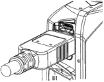
Then, the state when utilizing Fig. 8 A to Fig. 8 C explanation to use external interface.As mentioned above, the USB connector 11 of camera body and HDMI connector 12 have been installed to and have been configured in the side of camera body.Fig. 8 A illustrates the state that socket lid 6 has removed from camera body.In the time that socket cover removes, the end of the end of USB connector 11 and HDMI connector 12 exposes from socket pedestal 70, and socket pedestal 70 has the peristome 71 mating with the profile of each connector.By the USB cable 80 corresponding with USB connector 11 is inserted in USB connector 11, can carry out data communication (referring to Fig. 8 B) with external device (ED).Similarly, by the HDMI cable 81 corresponding with HDMI connector 12 is inserted in HDMI connector 12, can carry out data communication (referring to Fig. 8 C) with external device (ED).
According to the structure of above-mentioned illustrative embodiments, can provide following a kind of electronic equipment: even for the printed wiring board with many difference transmission lines, described electronic equipment still can prevent the generation of impedance mismatching and the generation of minimizing noise, and does not increase the quantity of connector signal.
Although preferred illustrative embodiments of the present invention has been described above, the present invention is not limited to this.In main idea of the present invention, can carry out multiple modification and change.
Although the present invention has been described with reference to illustrative embodiments, it should be understood that, the invention is not restricted to disclosed illustrative embodiments.The scope of appending claims should meet the most wide in range explanation, to contain all modification, equivalent structure and function.
Claims (8)
1. an electronic equipment, it comprises:
The first wiring plate, it is formed as having first area, second area and the 3rd region, wherein said first area is formed as extending along first direction from described the 3rd region, and described second area is formed as extending along the second direction contrary with described first direction from described the 3rd region;
The second wiring plate, it is connected to described the first wiring plate;
The first connector, it is for being connected to external device (ED), and wherein said the first connector is installed in the described first area of described the first wiring plate;
The second connector, it is for being connected to external device (ED), and wherein said the second connector is installed in the described second area of described the first wiring plate; And
The 3rd connector, it is connected to described the second wiring plate, and wherein said the 3rd connector is installed in described the 3rd region of described the first wiring plate, and described the 3rd connector is formed with the first terminal row and the second terminal that face with each other and is listed as,
Wherein, on described the first wiring plate, the first difference transmission lines is formed on the scope from described the first connector to described the first terminal row, and the second difference transmission lines is formed on the scope from described the second connector to described the second terminal row,
The mode that is configured to not face each other with the terminal being connected with described the second difference transmission lines in the terminal being connected with described the first difference transmission lines in described the first terminal row and described the second terminal row forms described the first difference transmission lines and described the second difference transmission lines.
2. electronic equipment according to claim 1, it is characterized in that, the mode that is configured to face with each other with the earth terminal in the terminal being connected with described the first difference transmission lines in described the first terminal row and described the second terminal row forms described the first difference transmission lines and described the second difference transmission lines.
3. electronic equipment according to claim 1, it is characterized in that, described the 3rd region has angular shape, described the first difference transmission lines and described the second difference transmission lines is connected up the closer to the inner side of described angular shape, the mode that this difference transmission lines just has more roundabout amounts with difference transmission lines.
4. electronic equipment according to claim 1, is characterized in that, described the first difference transmission lines and described the second difference transmission lines are adjusted to has the impedance differing from one another.
5. electronic equipment according to claim 1, is characterized in that, described the first connector is USB connector, and described the second connector is HDMI connector, and described the 3rd connector is mother daughter board connector.
6. electronic equipment according to claim 2, is characterized in that, described the first difference transmission lines is grounded pattern protection in both sides, and described the second difference transmission lines is grounded pattern protection in both sides.
7. electronic equipment according to claim 6; it is characterized in that; described the first wiring plate has the back side, and described the first difference transmission lines is grounded pattern protection in the projection at the described back side, and described the second difference transmission lines is grounded pattern protection in the projection at the described back side.
8. electronic equipment according to claim 1, is characterized in that, described the second difference transmission lines is many second difference transmission lines, and each the second difference transmission lines has identical length of arrangement wire.
Applications Claiming Priority (2)
| Application Number | Priority Date | Filing Date | Title |
|---|---|---|---|
| JP2010-169696 | 2010-07-28 | ||
| JP2010169696A JP5574867B2 (en) | 2010-07-28 | 2010-07-28 | Electronics |
Publications (2)
| Publication Number | Publication Date |
|---|---|
| CN102348052A CN102348052A (en) | 2012-02-08 |
| CN102348052B true CN102348052B (en) | 2014-06-04 |
Family
ID=45527182
Family Applications (1)
| Application Number | Title | Priority Date | Filing Date |
|---|---|---|---|
| CN201110212321.4A Active CN102348052B (en) | 2010-07-28 | 2011-07-27 | Electronic apparatus |
Country Status (3)
| Country | Link |
|---|---|
| US (1) | US8187013B2 (en) |
| JP (1) | JP5574867B2 (en) |
| CN (1) | CN102348052B (en) |
Families Citing this family (12)
| Publication number | Priority date | Publication date | Assignee | Title |
|---|---|---|---|---|
| US9225101B2 (en) * | 2010-07-14 | 2015-12-29 | Norman R BYRNE | Horizontal T-junction block assembly |
| CN103477505A (en) * | 2011-01-05 | 2013-12-25 | 汤姆逊许可公司 | Electronic device with PCBs interconnected by a flex circuit with controlled impedance |
| CN102725924A (en) * | 2012-02-23 | 2012-10-10 | 华为技术有限公司 | Interconnection board and server system |
| TWI593329B (en) | 2013-09-24 | 2017-07-21 | 聯詠科技股份有限公司 | Layout method, electronic device, and connector |
| CN104518387B (en) * | 2013-09-27 | 2018-03-13 | 联咏科技股份有限公司 | Wiring method, electronic installation and connector |
| TWI573503B (en) * | 2014-06-09 | 2017-03-01 | The Power Supply Path Structure of Soft Circuit Board | |
| JP3204474U (en) * | 2016-03-16 | 2016-06-02 | 裕雄 范 | Charging joint |
| JP7061459B2 (en) * | 2017-12-25 | 2022-04-28 | 日本航空電子工業株式会社 | Circuit board, connector assembly and cable harness |
| JP6679662B2 (en) * | 2018-06-25 | 2020-04-15 | キヤノン株式会社 | Imaging device |
| US10826243B2 (en) * | 2018-08-28 | 2020-11-03 | Sure-Fire Electrical Corporation | Electric connector terminal configuration structure |
| JP7346069B2 (en) * | 2019-04-25 | 2023-09-19 | キヤノン株式会社 | Electronics |
| JPWO2021002241A1 (en) * | 2019-07-04 | 2021-01-07 |
Family Cites Families (21)
| Publication number | Priority date | Publication date | Assignee | Title |
|---|---|---|---|---|
| US3696319A (en) * | 1970-08-20 | 1972-10-03 | Berg Electronics Inc | Flat conductor cable connector |
| US5013252A (en) * | 1990-01-18 | 1991-05-07 | Herman Miller, Inc. | Electrified wall panel system |
| US5096434A (en) * | 1990-08-22 | 1992-03-17 | Byrne Norman R | Electrical interconnection assembly |
| US5164544A (en) * | 1991-03-13 | 1992-11-17 | Westinghouse Electric Corp. | Electrified space dividing panel |
| US5252086A (en) * | 1992-05-28 | 1993-10-12 | Steelcase Inc. | Modular powerway with selectable receptacle |
| US6638111B1 (en) * | 2002-07-11 | 2003-10-28 | Molex Incorporated | Board mounted electrical connector with improved ground terminals |
| US7627343B2 (en) * | 2003-04-25 | 2009-12-01 | Apple Inc. | Media player system |
| JP4150977B2 (en) * | 2004-09-30 | 2008-09-17 | 株式会社村田製作所 | Wiring pattern structure of differential transmission path |
| CA2605084C (en) * | 2005-04-29 | 2013-11-05 | Norman R. Byrne | Center connect single-sided junction block |
| JP2007166290A (en) | 2005-12-14 | 2007-06-28 | Sony Corp | Imaging device |
| CN2886929Y (en) * | 2005-12-28 | 2007-04-04 | 华为技术有限公司 | Interconnecting device between interface boards of ultra transmission bus |
| JP5100449B2 (en) * | 2008-03-05 | 2012-12-19 | キヤノン株式会社 | Composite connector and electronic device including the same |
| JP2010074095A (en) * | 2008-09-22 | 2010-04-02 | Toshiba Corp | Electric circuit device |
| CN101860047B (en) * | 2009-04-11 | 2014-07-23 | 鸿富锦精密工业(深圳)有限公司 | Charging system and corresponding electronic device as well as charging device and automatic power off method |
| US7727028B1 (en) * | 2009-07-14 | 2010-06-01 | Hon Hai Precision Ind. Co., Ltd. | Electrical connector with contact terminals designed to improve impedance |
| EP2346121B1 (en) * | 2009-10-30 | 2015-06-17 | Panasonic Corporation | Receptacle and electronic apparatus |
| US8267728B2 (en) * | 2010-02-18 | 2012-09-18 | Panasonic Corporation | Receptacle, printed wiring board, and electronic device |
| US20110201215A1 (en) * | 2010-02-18 | 2011-08-18 | Panasonic Corporation | Receptacle, printed wiring board, and electronic device |
| JP5009388B2 (en) * | 2010-02-18 | 2012-08-22 | パナソニック株式会社 | Receptacle, printed wiring board, and electronic equipment |
| USD639736S1 (en) * | 2010-06-21 | 2011-06-14 | Kerio Technologies, Inc. | Power adapter |
| US8079846B1 (en) * | 2010-09-24 | 2011-12-20 | Mindray Ds Usa, Inc. | Rotatable electrical connector |
-
2010
- 2010-07-28 JP JP2010169696A patent/JP5574867B2/en active Active
-
2011
- 2011-07-21 US US13/188,238 patent/US8187013B2/en active Active
- 2011-07-27 CN CN201110212321.4A patent/CN102348052B/en active Active
Also Published As
| Publication number | Publication date |
|---|---|
| JP5574867B2 (en) | 2014-08-20 |
| US8187013B2 (en) | 2012-05-29 |
| US20120028481A1 (en) | 2012-02-02 |
| CN102348052A (en) | 2012-02-08 |
| JP2012033570A (en) | 2012-02-16 |
Similar Documents
| Publication | Publication Date | Title |
|---|---|---|
| CN102348052B (en) | Electronic apparatus | |
| US7345555B2 (en) | Writing pattern structure of differential transmission paths | |
| US6913487B2 (en) | Plug-in connector module | |
| TWI412182B (en) | Electrical connector with crosstalk canceling features | |
| US5030123A (en) | Connector and patch panel for digital video and data | |
| US5808876A (en) | Multi-function power distribution system | |
| US8277251B2 (en) | Electrical connector assembly with improved PCB engaging with a case | |
| US6368120B1 (en) | High speed connector and circuit board interconnect | |
| US7086869B1 (en) | Flexible cable interconnect with integrated EMC shielding | |
| US20140073181A1 (en) | Ground unit and electrical connector using same | |
| JP2019505043A (en) | Integrated routing assembly and system using the same | |
| US20070232089A1 (en) | Bridge modules for connecting plural groups of electronic modules | |
| JP5199479B2 (en) | Computer bus with configurable configuration | |
| JP2014509447A (en) | Controlled impedance flexible circuit | |
| US9799995B1 (en) | Dual unibody USB connector | |
| US20200099174A1 (en) | Io integration with floating connectors in a mesh | |
| US7170753B2 (en) | Interface enhancement for modular platform applications | |
| US7282649B2 (en) | Printed circuit board | |
| US10709013B2 (en) | Multilayer wiring board and differential transmission module | |
| US8460029B1 (en) | Stacked multi-port connector | |
| JP4829514B2 (en) | Card edge type board connector | |
| US20060270251A1 (en) | Low profile structure | |
| US9692192B2 (en) | Multi connector, wiring method thereof and display apparatus having the same | |
| US20030129865A1 (en) | Connective apparatus in which a number of contacts are grouped into a plurality of contact groups according to intended use | |
| US9282671B2 (en) | Tilted printed circuit board installation |
Legal Events
| Date | Code | Title | Description |
|---|---|---|---|
| C06 | Publication | ||
| PB01 | Publication | ||
| C10 | Entry into substantive examination | ||
| SE01 | Entry into force of request for substantive examination | ||
| C14 | Grant of patent or utility model | ||
| GR01 | Patent grant |