CN101866126B - Recording sheet surface detection apparatus and image forming apparatus - Google Patents
Recording sheet surface detection apparatus and image forming apparatus Download PDFInfo
- Publication number
- CN101866126B CN101866126B CN2010101642430A CN201010164243A CN101866126B CN 101866126 B CN101866126 B CN 101866126B CN 2010101642430 A CN2010101642430 A CN 2010101642430A CN 201010164243 A CN201010164243 A CN 201010164243A CN 101866126 B CN101866126 B CN 101866126B
- Authority
- CN
- China
- Prior art keywords
- image
- recording sheet
- light
- light beam
- exemplary embodiment
- Prior art date
- Legal status (The legal status is an assumption and is not a legal conclusion. Google has not performed a legal analysis and makes no representation as to the accuracy of the status listed.)
- Active
Links
Images


Classifications
-
- G—PHYSICS
- G03—PHOTOGRAPHY; CINEMATOGRAPHY; ANALOGOUS TECHNIQUES USING WAVES OTHER THAN OPTICAL WAVES; ELECTROGRAPHY; HOLOGRAPHY
- G03G—ELECTROGRAPHY; ELECTROPHOTOGRAPHY; MAGNETOGRAPHY
- G03G15/00—Apparatus for electrographic processes using a charge pattern
-
- G—PHYSICS
- G03—PHOTOGRAPHY; CINEMATOGRAPHY; ANALOGOUS TECHNIQUES USING WAVES OTHER THAN OPTICAL WAVES; ELECTROGRAPHY; HOLOGRAPHY
- G03G—ELECTROGRAPHY; ELECTROPHOTOGRAPHY; MAGNETOGRAPHY
- G03G15/00—Apparatus for electrographic processes using a charge pattern
- G03G15/60—Apparatus which relate to the handling of originals
- G03G15/607—Apparatus which relate to the handling of originals for detecting size, presence or position of original
-
- B—PERFORMING OPERATIONS; TRANSPORTING
- B41—PRINTING; LINING MACHINES; TYPEWRITERS; STAMPS
- B41J—TYPEWRITERS; SELECTIVE PRINTING MECHANISMS, i.e. MECHANISMS PRINTING OTHERWISE THAN FROM A FORME; CORRECTION OF TYPOGRAPHICAL ERRORS
- B41J11/00—Devices or arrangements of selective printing mechanisms, e.g. ink-jet printers or thermal printers, for supporting or handling copy material in sheet or web form
- B41J11/009—Detecting type of paper, e.g. by automatic reading of a code that is printed on a paper package or on a paper roll or by sensing the grade of translucency of the paper
-
- G—PHYSICS
- G03—PHOTOGRAPHY; CINEMATOGRAPHY; ANALOGOUS TECHNIQUES USING WAVES OTHER THAN OPTICAL WAVES; ELECTROGRAPHY; HOLOGRAPHY
- G03G—ELECTROGRAPHY; ELECTROPHOTOGRAPHY; MAGNETOGRAPHY
- G03G15/00—Apparatus for electrographic processes using a charge pattern
- G03G15/50—Machine control of apparatus for electrographic processes using a charge pattern, e.g. regulating differents parts of the machine, multimode copiers, microprocessor control
- G03G15/5029—Machine control of apparatus for electrographic processes using a charge pattern, e.g. regulating differents parts of the machine, multimode copiers, microprocessor control by measuring the copy material characteristics, e.g. weight, thickness
-
- G—PHYSICS
- G03—PHOTOGRAPHY; CINEMATOGRAPHY; ANALOGOUS TECHNIQUES USING WAVES OTHER THAN OPTICAL WAVES; ELECTROGRAPHY; HOLOGRAPHY
- G03G—ELECTROGRAPHY; ELECTROPHOTOGRAPHY; MAGNETOGRAPHY
- G03G21/00—Arrangements not provided for by groups G03G13/00 - G03G19/00, e.g. cleaning, elimination of residual charge
-
- G—PHYSICS
- G06—COMPUTING; CALCULATING OR COUNTING
- G06T—IMAGE DATA PROCESSING OR GENERATION, IN GENERAL
- G06T1/00—General purpose image data processing
-
- G—PHYSICS
- G03—PHOTOGRAPHY; CINEMATOGRAPHY; ANALOGOUS TECHNIQUES USING WAVES OTHER THAN OPTICAL WAVES; ELECTROGRAPHY; HOLOGRAPHY
- G03G—ELECTROGRAPHY; ELECTROPHOTOGRAPHY; MAGNETOGRAPHY
- G03G2215/00—Apparatus for electrophotographic processes
- G03G2215/00362—Apparatus for electrophotographic processes relating to the copy medium handling
- G03G2215/00535—Stable handling of copy medium
- G03G2215/00611—Detector details, e.g. optical detector
- G03G2215/00616—Optical detector
-
- G—PHYSICS
- G03—PHOTOGRAPHY; CINEMATOGRAPHY; ANALOGOUS TECHNIQUES USING WAVES OTHER THAN OPTICAL WAVES; ELECTROGRAPHY; HOLOGRAPHY
- G03G—ELECTROGRAPHY; ELECTROPHOTOGRAPHY; MAGNETOGRAPHY
- G03G2215/00—Apparatus for electrophotographic processes
- G03G2215/00362—Apparatus for electrophotographic processes relating to the copy medium handling
- G03G2215/00535—Stable handling of copy medium
- G03G2215/00717—Detection of physical properties
- G03G2215/00751—Detection of physical properties of sheet type, e.g. OHP
Landscapes
- Physics & Mathematics (AREA)
- General Physics & Mathematics (AREA)
- Engineering & Computer Science (AREA)
- Microelectronics & Electronic Packaging (AREA)
- Theoretical Computer Science (AREA)
- Control Or Security For Electrophotography (AREA)
- Length Measuring Devices By Optical Means (AREA)
- Controlling Sheets Or Webs (AREA)
- Investigating Or Analysing Materials By Optical Means (AREA)
- Investigating Materials By The Use Of Optical Means Adapted For Particular Applications (AREA)
Abstract
The patent provides a recording sheet surface detection apparatus and an image forming apparatus. An image forming apparatus for detecting surface conditions of a recording sheet on which an image is formed, includes a light source configured to emit a first light beam and a second light beam, an image capture device configured to capture a first image of a surface of the recording sheet illuminated with the first light beam and a second image of the surface of the recording sheet illuminated with the second light beam. A first straight line including a ray in a center of the first light beam and a second straight line including a ray in a center of the second light beam intersect with each other, when each straight line is projected onto the surface of the recording sheet, and a detection device configured to detect information about the unevenness on the surface of the recording sheet based on the first image and the second image.
Description
Technical field
The present invention relates to come the recording chart surface detection apparatus of the surface appearance of detection record sheet material, and relate to the image processing system that the result who detects based on the recording chart surface controls image forming conditions based on the surface image that forms by image capture apparatus.
Background technology
The image processing system of utilization such as duplicating machine and laser beam printer; The developed image visible through developing device is transferred on the recording sheet under predetermined transfer printing condition; And, under predetermined fixing conditions, apply heat and pressure image with the transfer printing of the institute of photographic fixing in the above to recording sheet.
In the image processing system of routine of configuration thus, for example, on the guidance panel that is provided with above that by the size of user's setting recording sheet material and type (below, the type of recording sheet is called as paper mold).Based on the setting on the guidance panel, control transfer printing condition (transmission speed of the recording sheet when comprising transfer bias and image transfer printing) and fixing conditions (transmission speed of the recording sheet when comprising fixing temperature and photographic fixing).
The open No.2004-38879 of Japanese patent application has discussed the technology that comprises following aspect: catch the surface appearance of recording sheet through using area sensor; Detect surface smoothness from the surface image of catching; Confirm the paper mold of recording sheet; Control transfer printing condition and/or fixing conditions with the result who confirms based on paper mold.Because the shade by concave-convex surface produces is directly caught, therefore thisly confirm aspect the precision very excellent in paper mold through the technology of using area sensor to catch the surface image of recording sheet.Especially, in the time can clearly distinguishing the having or not of concave-convex surface, size and the degree of depth with visual manner, for example, when distinguishing coated paper and uncoated paper (common paper), this method provides high paper mold to confirm precision.
But when confirming general office with the paper mold of recording sheet, for example, the shade situation that is produced by concave-convex surface depends on the fiber configuration greatly and promptly makes the direction of paper (below, be called fiber and dispose direction).Particularly, when from the direction that intersects vertically with fiber configuration direction during with rayed paper surface, the image of catching provides the high-contrast of emphasical concave-convex surface.But when from the direction identical with fiber configuration direction during with rayed paper surface, because the shade that is produced by concave-convex surface is not obvious, so the image of catching provides low contrast.Therefore, even for the paper of same type, the contrast of the image of catching is also different greatly, thus cause vertical sheet material through and the Different Results confirmed of paper mold between laterally sheet material passes through.
Utilize the technology among the open No.2004-38879 of Japanese patent application; Fiber configuration direction in nearly all paper mold meets under the prerequisite of the angular range from 0 (unanimity) to ± 15 degree about recording sheet transmission direction or perpendicular crossing direction; Especially, use rayed recording sheet with 15~70 degree from vergence direction about the recording sheet transmission direction.The image in this rayed zone is caught to improve paper mold by area sensor and is confirmed precision.But the fiber configuration direction of recording sheet depends on the match ratio of raw material in the manufacture process.But, in recent years, make recording chart through the different manufacture processes of various manufacturing locations, this causes different fiber configuration directions.Therefore, fiber configuration direction may not be about the vertical or horizontal angular range that meets from 0 (unanimity) to ± 15 degree of recording sheet.Therefore; Utilize catching among the open No.2004-38879 of Japanese patent application to use from the technology of the surface image in light-struck zone of a direction, identical recording sheet possibly provide the definite Different Results of paper mold according to the relation that fiber disposes between direction and the rayed direction.
Summary of the invention
The present invention is intended to reduce the variation of the testing result that is caused by the fiber configuration direction of recording sheet and the relation between the rayed direction, and the paper mold that has the recording sheet of any fiber configuration direction with raising is confirmed precision.
Through the following explanation with reference to the advantages exemplary embodiment, it is obvious that further feature of the present invention will become.
Description of drawings
Be contained in the instructions and constitute its a part of accompanying drawing exemplary embodiment of the present invention, characteristic and many aspects are shown, and be used to explain principle of the present invention with explanation.
Figure 1A is the sectional drawing that forms device according to the coloured image of first exemplary embodiment.
Figure 1B is the block diagram that illustrates according to the action control of the image processing system of first exemplary embodiment.
Fig. 2 A is the skeleton view according to the recording chart surface detection apparatus of first exemplary embodiment.
Fig. 2 B is the top view according to the recording chart surface detection apparatus of first exemplary embodiment.
Fig. 2 C is the sectional drawing according to the recording chart surface detection apparatus of first exemplary embodiment.
Fig. 3 A illustrates from the concave-convex surface image in the zone of the light-struck paper mold of vertical usefulness (1) of paper.
Fig. 3 B illustrates from the concave-convex surface image in the zone of the light-struck paper mold of horizontal usefulness (1) of paper.
Fig. 4 A is the histogram that the Luminance Distribution of the concave-convex surface image among Fig. 3 A is shown.
Fig. 4 B is the histogram that the Luminance Distribution of the concave-convex surface image among Fig. 3 B is shown.
Fig. 5 is the diagrammatic sketch that the luminance difference testing result of paper mold (1) and (2) in first exemplary embodiment is shown.
Fig. 6 is the skeleton view according to the recording chart surface detection apparatus of the modification of first exemplary embodiment.
Fig. 7 A is the top view that the restriction condition of recording chart surface detection apparatus is shown.
Fig. 7 B is the sectional drawing that the restriction condition of recording chart surface detection apparatus is shown.
Fig. 8 is the top view according to the recording chart surface detection apparatus of second exemplary embodiment
Fig. 9 A is the skeleton view according to the recording chart surface detection apparatus of the 3rd exemplary embodiment.
Fig. 9 B is the top view according to the recording chart surface detection apparatus of the 3rd exemplary embodiment.
Fig. 9 C is the side view according to the recording chart surface detection apparatus of the 3rd exemplary embodiment.
Figure 10 A illustrates from the concave-convex surface image in the zone of the light-struck paper mold of vertical usefulness (1) of paper.
Figure 10 B illustrates from the concave-convex surface image in the zone of the light-struck paper mold of horizontal usefulness (1) of paper.
Figure 11 is the top view according to the recording chart surface detection apparatus of first modification of the 3rd exemplary embodiment.
Figure 12 is the top view according to the recording chart surface detection apparatus of second modification of the 3rd exemplary embodiment.
Figure 13 is the top view according to the recording chart surface detection apparatus of the 3rd modification of the 3rd exemplary embodiment.
Figure 14 A is the skeleton view according to the recording chart surface detection apparatus of the 4th exemplary embodiment, and Figure 14 B is the top view according to the recording chart surface detection apparatus of the 4th exemplary embodiment.
Figure 14 C is the side view according to the recording chart surface detection apparatus of the 4th exemplary embodiment.
Figure 15 A is the front elevation according to the recording chart surface detection apparatus of the modification of the 4th exemplary embodiment.
Figure 15 B is the side view according to the recording chart surface detection apparatus of the 4th exemplary embodiment.
Figure 16 is the top view as the recording chart surface detection apparatus of the comparative pattern of first exemplary embodiment.
Figure 17 is the diagrammatic sketch that the luminance difference testing result of paper mold (1) and (2) in the comparative pattern of first exemplary embodiment is shown.
Figure 18 is the top view that the problem of recording chart surface detection apparatus is shown.
Figure 19 is the top view that the problem of recording chart surface detection apparatus is shown.
Embodiment
Below, with each exemplary embodiment, characteristic and the many aspects that present invention will be described in detail with reference to the accompanying.
But, the invention is not restricted to the exemplary embodiment of following explanation; Especially, can revise size, material, shape and the relative position of the parts in the exemplary embodiment of following explanation in a different manner according to using device of the present invention and various condition.
Below explanation is comprised the image processing system of the recording chart surface detection apparatus of first exemplary embodiment according to the present invention.At first explanation is comprised the image processing system according to the recording chart surface detection apparatus of first exemplary embodiment.Then, the recording chart surface detection apparatus that detailed description is used for this image processing system.
Can for example form the recording chart surface detection apparatus that uses in the device according to first exemplary embodiment at electronic photograph color image.Figure 1A illustrates the sectional drawing of the internal configurations of the cascade connection type coloured image formation device of the use intermediate transfer belt of property electronic photograph color image formation device as an example.
Coloured image shown in Figure 1A forms device and has four handle boxes 31 (31Y, 31M, 31C and 31Bk) that constitute first to the 4th image formation unit respectively.These four image formation units form yellow, magenta, cyan and black image respectively, and except the toner color, have identical configuration.With reference to Figure 1A, symbol Y, M, C and Bk represent respectively to form the unit corresponding components with yellow, magenta, cyan and black image.But in following explanation, in the time need not distinguishing color especially, symbol Y, M, C and Bk are omitted.
Below will be with reference to the action of Figure 1A explanation according to the image formation unit of the image processing system of this exemplary embodiment.When control module 10 receives print image signal, see recording sheet P from sheet material box 15 to image formation unit to 18 with delivery roll to 17 through feed rolls.Then, recording sheet P was once stopped 19a and 19b by opposing roller (resist roller), and the opposing roller is used to make image to form the transmission unit of the transmitting synchronous of action (afterwards stating) and recording sheet P to 19a and 19b.
Simultaneously, control module 10 is carried out exposure on the surface of photosensitive drums 1, to form electrostatic latent image according to the picture signal indication exposure scanner unit 11 that receives, and photosensitive drums 1 is to be recharged the photosensitive-member that roller 2 is charged to fixed potential.The driving force of driving motor (not shown) is transferred to photosensitive drums 1 so that itself and image form action synchronously along turning clockwise.
Developer unit 8 is to be used for latent electrostatic image developing so that its visible unit.Developer unit 8 has and is applied in the development bias voltage so that the visible development sleeve 5 of electrostatic latent image.Like this, because the effect of developer unit 8, the electrostatic latent image that on the surface of photosensitive drums 1, forms is developed and is toner image.Photosensitive drums 1, charged roller 2 and developer unit 8 are integrated in the handle box 31 that removably is attached on the image processing system.
With each intermediate transfer belt that contacts 24 in the photosensitive drums 1 when coloured image forms and among photosensitive drums 1Y, 1M, 1C and the 1Bk rotation of each synchronously be rotated counterclockwise.Be transferred in succession on the intermediate transfer belt 24 at the color toner image that develops on each photosensitive drums, and the active layer of the primary transfer bias voltage through being applied to primary transfer roller 4 is stacked in over each otherly, on intermediate transfer belt 24, produces the multi-color toner image thus.Then, the multi-color toner image that on intermediate transfer belt 24, forms is transferred to and comprises secondary transfer roller to 25 secondary transfer printing retained part.Simultaneously, recording sheet P that 19a and 19b is stopped by roller and the ground of the multi-color toner image synchronization on the intermediate transfer belt 24 are transferred to the secondary transfer printing retained part through the opposing roller to the effect of 19a and 19b.Through being applied to the effect of secondary transfer roller to the secondary transfer printing bias voltage on 25, the multi-color toner image on the intermediate transfer belt 24 is transferred on the recording sheet P in the lump.
Fixation unit 21 in transmission log sheet material P with the multi-color toner image fusion of transfer printing and photographic fixing to recording sheet P.Shown in Figure 1A, fixation unit 21 have be used for to recording sheet P apply heat warm-up mill 21a exert pressure so that its pressure roll 21b that contacts with warm-up mill 21a to it with being used for.In through warm-up mill 21a and pressure roll 21b transmission maintenance multi-color toner record images sheet material P, apply heat and pressure to recording sheet P, make toner image by photographic fixing to the surface of recording sheet P.After toner image was by photographic fixing, recording sheet P was discharged in the discharge dish 16 20 through distributing roller, accomplished image thus and formed action.
Cleaning unit 28 is removed residual toner with cleaning band from middle transfer belt 24, and the remaining toner of removal is used as used toner and leaves in the cleaner container 29.
Control module 10 through being contained in the image processing system is carried out above-mentioned image formation action.
In the image processing system in Figure 1A, be set at the opposing roller to the upstream side of recording sheet transmission direction (that is, along) before 19a and the 19b according to the recording chart surface detection apparatus 40 of this exemplary embodiment.Recording chart surface detection apparatus 40 can detect the information about the concave-convex surface (surface smoothness) of the recording sheet P that transmits from sheet material box 15.From sheet material box 15 after image formation unit is seen recording sheet P off, when opposing roller that recording sheet P is used as transmission unit stops 19a and 19b, the surface appearance of recording chart surface detection apparatus 40 detection record sheet material P.
Figure 1B is the control block diagram that the action control of image processing system is shown.Based on the detection information that the driving computing unit 40C from recording chart surface detection apparatus 40 sends, control module 10 is controlled the image forming conditions of each image formation unit best with the operation image processing system.Especially, comprise secondary transfer roller to 25 secondary transfer printing bias voltage and the fixing temperature that is contained in the warm-up mill 21a in the fixation unit 21 by the image forming conditions of control module 10 control.
Recording chart surface detection apparatus 40 according to first exemplary embodiment below will be described.Fig. 2 A~2C illustrates the configured in one piece of the image of the concave-convex surface that is used to catch recording sheet P.Fig. 2 A is the skeleton view of recording chart surface detection apparatus 40, and Fig. 2 B is its top view, and Fig. 2 C is its sectional drawing that cuts along the A-A ' line among Fig. 2 B.Comprise as irradiation luminous diode (LED) 42A of light source and 42B, as the CMOS area sensor 43A of image-capture device and 43B and as the imaging len 44SA and the 44SB of imaging means according to the recording chart surface detection apparatus 40 of this exemplary embodiment.Recording chart surface detection apparatus 40 is set to the image formation surface in the face of recording sheet P.For the ease of explanation, in Fig. 2 A~2C, the recording chart surface detection apparatus 40 among Figure 1A is rotated 180 degree (turning upside down).
As the irradiation LED 42A and the 42B that in this exemplary embodiment, use, use White LED (from the product No.NSPW300DS of Nichia Corporation) with high directivity.Shown in Fig. 2 A and Fig. 2 B, irradiation LED 42A is set to first light source, makes that the straight line of the optical axis project to first light source on the recording sheet P is consistent with the recording sheet transmission direction.And irradiation LED 42B is set to secondary light source, makes that the straight line of the optical axis project to the secondary light source on the recording sheet P is vertical with the recording sheet transmission direction.Shown in Fig. 2 C, be irradiated on the surface of recording sheet P from two light beams of two light sources incident angle with 15 degree.Through light shining on the surface of recording chart with little incident angle by this way, make it possible to stress shade by the generation of the concave-convex surface on the recording sheet P.For the shade of stressing to produce, hope with little incident angle with rayed paper surface from 0 (not comprising) to 20 degree (comprising) by the concave-convex surface on the recording sheet P.
From specific direction with rayed recording sheet P, and, produce shade by the concave-convex surface on it.Folded light beam from produce the zone of shade through rayed is assembled and is drawn towards respectively then CMOS area sensor 43A and 43B through imaging len 44SA and 44SB.Catch each regional image of the lip-deep preliminary dimension of recording sheet P as the CMOS area sensor 43A of first area sensor with as among the CMOS area sensor 43B of second area capture device each through using each folded light beam.Folded light beam reflection recording sheet P is lip-deep through the concave-convex surface (surface smoothness) in each zone of rayed generation shade.Among CMOS area sensor 43A and the 43B each is respectively caught each pixel in the image for said zone, detects the image voltage signal that changes according to reflection light quantity, and it is outputed to drives computing unit 40C.In case receive the image voltage signal from CMOS area sensor 43A and 43B; The A/D conversion of just carrying out signal as the driving and the arithmetic element 40C of detecting device; 256 gray scale digital signals (monochrome information) after the A/D conversion are calculated contrast (luminance difference), and the contrast that obtains is outputed to control module 10.Particularly, the driving computing unit 40C as detecting device detects the contrast by the surface image of catching as the CMOS area sensor 43 of image-capture device.Drive light quantity and luminous timing that computing unit 40C also drove and controlled irradiation LED 42.CMOS area sensor 43 is contained in the recording chart surface detection apparatus 40 with driving computing unit 40C.
In this exemplary embodiment, CMOS area sensor 43A has 1.5mm (the vertical) * valid pixel size of 1.5mm (level) and the resolution of 600dpi with 43B.With imaging len 44SA and 44SB combination, can catch the zone of size of the lip-deep 3.0mm of having (the vertically) * 3.0mm (level) of recording sheet with the resolution of 300dpi.Area sensor refer to can be once two dimension catch information about the sensor of the pixel of the pixel of a plurality of arranged perpendicular and a plurality of horizontal arrangement.Shown in Fig. 2 A~2C, CMOS area sensor 43A and 43B are set at and use from (along the position of the direction that roughly intersects with the Surface Vertical of recording sheet P) under light-struck zone of irradiation LED 42A and 42B.Especially, after being assembled by imaging len 44SA and 44SB from the folded light beam in rayed zone and being drawn towards CMOS area sensor 43A and 43B respectively then, optical axis is roughly crossing with the Surface Vertical of recording sheet P.
In this exemplary embodiment, with light beam irradiates recording sheet P, and CMOS area sensor 43A and 43B catch the regional surface image of each rayed from the both direction different with the fiber of recording sheet P configuration direction.In other words, make the lip-deep straight line that comprise first and second optical axises that project to recording sheet P intersect each other with the primary optic axis of the light beam that shines first rayed zone with from the secondary light source emission with second optical axis of the light beam that shines second rayed zone from first light emitted.Therefore; For example; Even the straight line of the optical axis of a light source on projecting to recording sheet P and fiber configuration direction is consistent and image that catch when therefore comparing the expression low contrast with concave-convex surface, project to another light source on the recording sheet P optical axis straight line also the edge direction orientation different and the image of catching with fiber configuration direction therefore expression reflect the high-contrast of concave-convex surface.Therefore; Through for example all taking all factors into consideration these two images through making even; Can reduce the variation of the testing result that causes by the relation between the fiber of recording sheet P configuration direction and the rayed direction, the precision when improving the concave-convex surface of confirming on the recording sheet P thus.The mean direction of lip-deep each fiber of recording sheet in the fiber configuration direction indication recording sheet of recording sheet.
Below explanation is illustrated the exemplary embodiment of the effect of above-mentioned configuration.In experiment, use two kinds of different paper molds: (1) through the A4 size of along inclined direction cutting Ledger size common paper (Xerox Business (registered trademark) 4200 20Lb) and obtaining paper mold (1) and through paper mold (2) along the A4 size of the identical common paper acquisition of fiber configuration direction (vertically) cutting.The detection of paper mold (1) and (2) below will be described.When with microscopic examination A4 size paper mold (1), fiber configuration direction is about fore-and-aft tilt 20 degree of paper.Fig. 3 A and Fig. 3 B illustrate the image through the surface of using the paper mold (1) of catching according to the recording chart surface detection apparatus of this exemplary embodiment.Fig. 3 A illustrate by CMOS area sensor 43A catch from the vertical identical direction of paper concave-convex surface image with the zone of the preliminary dimension on light-struck paper mold (1) of irradiation LED 42A.Fig. 3 B illustrate by CMOS area sensor 43B catch from the vertical vertical direction (laterally) of paper concave-convex surface image with the zone of the preliminary dimension on light-struck paper mold (1) of irradiation LED 42B.Fig. 4 A and Fig. 4 B illustrate the monochrome information (digital signal level) of these concave-convex surface images with histogrammic form.With reference to Fig. 4 A and Fig. 4 B, 256 gray scale intensities information (digital signal level) of transverse axis presentation surface bump maps picture, the longitudinal axis representes to show as the pixel count in the capture region of frequency.
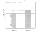
Drive computing unit 40C and calculate mean value Imax from the signal of five pixels with first to the 5th maximum brightness (ceiling voltage) information (digital signal level).Drive computing unit 40C and also calculate mean value Imin from the signal of five pixels with first to the 5th minimum brightness (minimum voltage) information.Drive computing unit 40C and obtain luminance difference Δ I for each image, that is, and the difference between Imax and the Imin.Fig. 5 illustrates the result of the luminance difference detection of above-mentioned A4 size paper mold (1) and (2).For example, from demonstrating tangible shade with the image in the zone of the rayed on light-struck paper mold (1), thereby big luminance difference Δ I (1) B is provided with the vertical vertical direction (laterally) of paper.On the contrary, from demonstrating unconspicuous shade with the image in the zone on light-struck paper mold (1), thereby little luminance difference Δ I (1) A is provided with the vertical identical direction of paper.Drive computing unit 40C and obtain Δ I (1) A and Δ I (1) B, and calculate its mean luminance differences Δ I (1) (ave).Similarly, drive computing unit 40C and calculate mean luminance differences Δ I (2) (ave) from Δ I (2) A and Δ I (2) B for paper mold (2).As shown in Figure 5, the A4 size paper mold (2) of the vertical consistency of fiber configuration direction and paper provides big difference between Δ I (2) A and Δ I (2) B.On the contrary, fiber configuration direction provides little difference about the paper mold (1) of fore-and-aft tilt 20 degree of paper between Δ I (1) A and Δ I (1) B.This means that the luminance difference in each concave-convex surface image depends on the fiber configuration direction of paper.On the other hand, the mean luminance differences Δ I (ave) of each converges to value much at one in paper mold (1) and (2).This means and to reduce the dependence of testing result through catching the image of using from light-struck two rayed zone of two Different Light for fiber configuration direction.
As the comparative pattern of this exemplary embodiment, on the basis of experiment, make the recording chart surface detection apparatus (catching image) of known general type based on a light source and one.Then, shown in figure 16, detect through using above-mentioned two A4 size paper molds (1) and (2) to carry out the paper surface.Owing to tilt 45 degree about the recording sheet transmission direction except irradiation LED 42 is provided so that the straight line that projects to its last optical axis of recording sheet (paper) P; Dispose this comparative pattern with the mode identical, the explanation of therefore omitting this comparative pattern with this exemplary embodiment.
Figure 17 illustrates the result who detects through the paper surface of using this recording chart surface detection apparatus to obtain.Detect with the paper surface of the paper mold (2) of the vertical consistency of A4 size paper with fiber configuration direction and to compare, fiber configuration direction detects about the paper surface of the paper mold (1) of fore-and-aft tilt 20 degree of A4 size paper much little luminance difference Δ I is provided.More specifically, though use identical paper mold, according to the fiber configuration direction of paper, comparative pattern provides the paper big different result that the surface is detected.
On the contrary, this exemplary embodiment makes it possible to reduce testing result for the dependence of the fiber configuration direction of recording sheet and therefore reduce the variation of testing result, improves concave-convex surface thus and confirms precision.
And in this exemplary embodiment, the primary optic axis of irradiation LED 42A is vertical with second optical axis of irradiation LED 42B.Utilizing should configuration, when a rayed zone catch the low luminance difference of graphical representation (contrast) time, the image of catching in another rayed zone is represented high luminance difference (contrast) without any exception.Therefore; In recording sheet with any fiber configuration direction, can be through using mean luminance differences Δ I (ave), promptly; Two mean values of catching the luminance difference (contrast) of image reduce the variation of the testing result that is caused by the fiber of recording sheet configuration direction most effectively.But primary optic axis may not be vertical with second optical axis.Can from the well-known configurations of routine (based on catching image with of light-struck zone of a light source) from a direction relatively understand this point.Therefore, through using from two different directions, can reduce the variation of testing result, and can improve concave-convex surface thus and confirm precision with light-struck two mean luminance differences Δ I (ave) that catch image with two zones of different shade conditions.Therefore, preferred disposition first and second light sources make that the straight line project to connection first light source and first rayed zone on the recording sheet P is crossing with the straight line that is connected secondary light source and second rayed zone on projecting to recording sheet P.
Utilize above-mentioned configuration, confirm through using two mean luminance differences Δ I (ave) that catch image.But the method for confirming is not limited to this method.As another method, for example, can be that Δ I (1) (a) adds that Δ I (1) luminance difference (b) confirms through using two luminance differences of combination.As replacement scheme, the combination of two luminance differences ratio can (a) change with Δ I (1) difference (b) according to said two luminance difference Δ I (1).And, can catch any in the image through use, for example confirm through the image of catching that uses big luminance difference.And, in the method, and only compared by method for imaging with a light-struck zone from a direction, obtain different definite results' possibility reduction about identical recording sheet.
Utilize above-mentioned configuration, though the first and second rayed zones are set on the surface of recording sheet P, not have the independent zone of lap,, these two zones can be provided so that they overlap each other.In this case, when the image of catching with a zone of a light source irradiation, another light source is not luminous.In other words, luminous timing is distinguished between irradiation LED 42A and 42B.Therefore, the timing of image capturing is also distinguished between the first and second rayed zones, that is, once catch for a regional carries out image.Owing to handle them with the mode identical, therefore omit said two explanations of catching image with above mode.
And, though two irradiation LED 42A and 42B are used as first and second light sources respectively,, as shown in Figure 6, as substituting of two irradiation LED 42A and 42B, can use irradiation LED 42.In this case, irradiation LED 42 can be along two different direction emission light beams to shine first and second rayed zone.
Though LED is used as light source in this exemplary embodiment,, for example, also can use xenon lamp or Halogen lamp LED as light source.In brief, just shine the ability of enough light quantities for the requirement of necessity of light source with the shade stressing to produce by the concave-convex surface on the recording sheet.And as substituting of area sensor, the line sensor that can use the pixel with edge direction configuration vertical with the recording sheet transmission direction is as image-capture device.Can in recording sheet transmission direction portable cord sensor, catch image.And,, can use CCD type sensor as substituting of CMOS type sensor.In brief, just catch the ability of the image of the concave-convex surface on the recording sheet for the requirement of necessity of image-capture device.
Though be used for detecting among the driving computing unit 40C of recording chart surface detection apparatus 40 that the measuring ability of the contrast of the surface image of being caught by CMOS area sensor 43 is contained in this exemplary embodiment, this function can be contained in the control module 10 of image processing system.In this exemplary embodiment, control module 10 is based on the result of the recording sheet concave-convex surface detection of recording chart surface detection apparatus 40, control transfer bias or fixing temperature.But controlling factor is not limited thereto, and various controlled variable and a series of images that control module 10 can also be controlled in each process that for example forms such as sub-image and develop form speed (processing speed).In brief, the relevant any image forming conditions of image formation unit that is used on recording sheet, forming image in control module 10 may command and the image processing system.
Based on clear specifically first exemplary embodiment of LED configuration, make when sending light beam with the inverted V-shaped shape when the downstream of recording sheet transmission direction is watched from irradiation LED 42A and 42B.Will be based on LED configuration instruction second exemplary embodiment of the modification of recording chart surface detection apparatus 40.In this exemplary embodiment, be endowed identical Reference numeral with element components identical in first exemplary embodiment, and will omit the explanation of repetition, the LED configuration will only be described below therefore.
Fig. 7 A and Fig. 7 B illustrate the variations according to the recording chart surface detection apparatus 40 of first exemplary embodiment among Fig. 2.Irradiation LED 42A and 42B be access areas sensor 43A and 43B and imaging len 44SA and 44SB more.Fig. 7 A is a top view, and Fig. 7 B is the sectional drawing that cuts along the A-A ' line among Fig. 7 A.With reference to Fig. 2 B and Fig. 7 A, the irradiation LED 42A from Fig. 7 A and 42B emission has the beam spread angle (α) bigger than the beam spread angle among Fig. 2 B with in the light beam of irradiates light irradiation area each.When light beam was expanded greatly by this way excessively, a rayed zone comprised high-contrast part and low contrast part simultaneously, and this has increased the complexity of definite algorithm, or has reduced concave-convex surface and confirmed precision.Therefore, irradiation LED 42A and 42B are divided to a certain extent respectively opens with area sensor 43A and 43B and imaging len 44SA and 44SB.Shown in Fig. 7 B, along the normal direction of recording sheet P, irradiation LED 42A and 42B can interfere near the transmission path (part X) of recording sheet P.This is to make irradiation LED 42A and 42B divide another reason of opening (restriction condition) with area sensor 43A and 43B and imaging len 44SA and 44SB to a certain extent.
In this exemplary embodiment, will consider that below this restriction condition explanation is used to make the LED configuration of recording sheet surface detection apparatus miniaturization.Fig. 8 is the top view according to the recording chart surface detection apparatus 40 of this exemplary embodiment.Two irradiation LED 42A and 42B preferably are set, make each light beam intersect each other.In other words, has the relation that makes that the straight line of lip-deep these optical axises of projecting to recording sheet P intersects each other from irradiation LED 42A emission with the optical axis of the light beam that shines second rayed zone with the optical axis of the light beam that shines first rayed zone with from irradiation LED 42B emission.These LED configurations make it possible to from the light source to the rayed, disposing the necessary parts that are used to form light path at least in the light path in zone compactly.Therefore, can reduce irradiation LED 42A and 42B and the first and second rayed zones, make it possible to realize the miniaturization of recording chart surface detection apparatus thus in the lip-deep projected area of recording sheet P.
Light path from the rayed zone to cmos sensor 43A and 43B below will be described.When projection cmos sensor 43A and 43B on the surface of recording sheet P; Each center in projection irradiation LED 42A, irradiation LED 42B, first rayed zone and second rayed zone on the surface of recording sheet P makes cmos sensor be preferably placed at through in the quadrilateral area that connects these four somes formation.When the normal direction of recording sheet P is watched, the cmos sensor 43A of configuration meets the scope that occupies to the regional light path of each rayed by from light source with the light path that 43B makes it possible to from the rayed zone to cmos sensor 43A and 43B by this way.In other words; When the normal direction of recording sheet P is watched; Can be through making light path with overlapping to the light path of cmos sensor 43A and 43B from the rayed zone from irradiation LED 42A and 42B to each rayed zone, minimizing recording chart surface detection apparatus is in the lip-deep view field of recording sheet P.As a result of, further miniaturization of whole recording chart surface detection apparatus.In this exemplary embodiment, similar with first exemplary embodiment, cmos sensor 43A and 43B be set at from each rayed zone to roughly with the position of the direction skew of the Surface Vertical of recording sheet on.Therefore, the light path from irradiation LED 42A and 42B to each rayed zone, the light path from the rayed zone to cmos sensor 43A and 43B and the necessary parts that are used to form these light paths satisfy above-mentioned condition.Compare with Fig. 2, comprise that under these conditions recording chart surface detection apparatus among Fig. 8 of irradiation LED 42A and 42B, the first and second rayed zones and cmos sensor 43A and 43B of configuration makes it possible to width is reduced to about 50% (from W to W * 0.5).
In this exemplary embodiment, can catch similarly from the image of two different directions with first exemplary embodiment with light-struck two zones of two light sources.This configuration makes it possible to reduce testing result for the dependence of the fiber configuration direction of recording sheet and therefore reduce the variation of testing result, improves concave-convex surface thus and confirms precision.And this exemplary embodiment can realize the miniaturization of recording chart surface detection apparatus.
Fig. 9 A is the skeleton view according to the recording chart surface detection apparatus of the 3rd exemplary embodiment, and Fig. 9 B is its top view, and Fig. 9 C is its side view.Comprise as the irradiation LED 42A of light source and 42B, as the shadow shield 46 of shading means, as the CMOS line sensor 43L of image-capture device with as the imaging len array 44A of imaging means according to the recording chart surface detection apparatus 40 of the 3rd exemplary embodiment.To be omitted with the explanation of element components identical in first exemplary embodiment.
In this exemplary embodiment, (model SLR343WBC7T is from ROHM Co., Ltd.) for using standard lamp type White LED as the irradiation LED 42A of light source and 42B.Shown in Fig. 9 A and Fig. 9 B; Be under the prerequisite of positive dirction in the clockwise direction; Irradiation LED 42A is set up as first light source, and the feasible straight line that projects to the optical axis of first light source on the recording sheet P is spent about recording sheet transmission direction inclination+45, and; Irradiation LED 42B is set up as secondary light source, and the feasible straight line that projects to the optical axis of the secondary light source on the recording sheet P is spent about recording sheet transmission direction inclination-45.This means, when when the downstream of recording sheet transmission direction is watched, with the optical axis of two light sources of inverted V-shaped shape configuration.Shown in Fig. 9 C, spend two zones shining on the same straight line that intersects vertically with the recording sheet transmission direction about the surface of recording sheet P with 15 from the light beam of two light sources.CMOS line sensor 43L and imaging len array 44A are provided so that their vertical and recording sheet transmission directions separately intersect vertically.This configuration makes it possible to realize the image capturing with two the rayed zones (first and second rayed zone) on the straight line that intersects vertically with the recording sheet transmission direction of irradiation LED 42A and 42B irradiation.The first and second rayed zones are different zones.
The folded light beam in the zone of the shadow information of the concave-convex surface (surface smoothness) on the next self-contained reflection recording sheet P is assembled through imaging len array 44A, and is caught by CMOS line sensor 43L as line image then.CMOS line sensor 43L detects the image voltage signal that each line for the pixel in the line image of catching changes according to reflection light quantity, and it is outputed to drives computing unit 40C.In case receive the image voltage signal from CMOS line sensor 43L, change to detect the digital signal (monochrome information) after A/D changes as the driving of detecting device and the A/D that arithmetic element 40C just carries out signal.In recording sheet transmission direction moving recording sheet material P, in the image capturing action of each line of pixel, digital signal (monochrome information) is connected to produce regional luminance information in succession.Drive computing unit 40C and calculate contrast (luminance difference), and it is outputed to control module 10 from zone digit signal (monochrome information).In other words, the driving computing unit 40C as detecting device detects the contrast that calculates from through the regional luminance information that connects the line image generation of being caught by the CMOS line sensor 43L as image-capture device in succession.CMOS line sensor 43L and driving computing unit 40C are contained in the recording chart surface detection apparatus 40.
The CMOS line sensor 43L that is used for this exemplary embodiment has the valid pixel length (vertically) of 20mm and the resolution of 600dpi.At recording sheet P through when 19a and 19b being transferred to secondary transfer printing pressing part as the opposing roller of transmission unit; Control module 10 is carried out above-mentioned image capturing action through making recording sheet P move 5mm along the recording sheet transmission direction for each line of pixel.More specifically; CMOS line sensor 43L catches the image of the line that connects following pixel as line image, and said pixel is the pixel of the preliminary dimension in the lip-deep second rayed zone of pixel and recording sheet P of the preliminary dimension in the lip-deep first rayed zone of recording sheet P.The opposing roller to 19a and 19b as transmission unit transmission log sheet material P in, CMOS line sensor 43L catches the image on the surface of recording sheet P successively, thus with the lip-deep 5 * 20mm of the resolution acquisition recording chart of 600 * 600dpi
2The monochrome information in zone.Line sensor refers to the sensor of line information of the pixel of the pixel that can catch an arranged perpendicular and a plurality of horizontal arrangement.Can also be vertically and a plurality of such line sensors of horizontal arrangement, to catch information simultaneously about a plurality of lines.Through using line sensor by this way, make it possible in transmission log sheet material P, realize the image capturing on the surface of recording sheet P.Therefore, compare with the situation of when recording sheet P stops, carrying out image capturing, can be under the condition of the turnout deterioration that does not make image processing system the surface appearance of detection record sheet material.
In through the area image of catching the action acquisition in succession for each line carries out image of pixel; 5 * 10mm, half zone is the shadow image that shines generation from the light of irradiation LED 42A through using, and another 5 * 10mm half zone is through using the shadow image from the rayed generation of irradiation LED 42B.Drive computing unit 40C regional through using light from irradiation LED 42A and 42B to shine in two and half area images of acquisition to extract 5 * 5mm near each the center.For example, Figure 10 A and Figure 10 B illustrate through with two surface images that like the technology type of first exemplary embodiment, obtain for the surface detection technique of A4 size paper mold (1).Drive computing unit 40C through with analytical technology like the technology type of first exemplary embodiment, the concave-convex surface on the detection record sheet material P.Control module 10 is based on the image forming conditions of testing result control such as the image formation unit of best transfer bias and fixing temperature.
As stated, in this exemplary embodiment, catch similarly from the image of two different directions with light-struck two zones of two light sources with first exemplary embodiment.This configuration makes it possible to reduce testing result for the dependence of the fiber configuration direction of recording sheet and therefore reduce the variation of testing result, improves concave-convex surface thus and confirms precision.
And, in this exemplary embodiment, shadow shield 46 is set to prevent will to use light-struck first and second rayed zone from other direction from the rayed of a direction, prevent that thus concave-convex surface from confirming the reduction of precision.
In this exemplary embodiment, though the shadow shield 46 that laterally arranges with the recording sheet transmission direction is used as the shading means, the shading means are not limited thereto.For example, shown in figure 11 as first modification of this exemplary embodiment, can the shadow shield 47 that comprise slit be set not parallelly with the recording sheet transmission direction, come as the shading means.Shadow shield 47 comprise be arranged on light from irradiation LED 42A advance to first light path in first rayed zone the first slit 47A be arranged on light and advance to the second slit 47B second light path in second rayed zone from irradiation LED 42B.Use comprises the shadow shield 47 of this slit, has reduced the restriction for the directivity of irradiation LED.This makes it possible to adjust more easily the optical axis of irradiation LED (light source), thereby helps the range of choice of expansion light source.
As the modification of first exemplary embodiment, as shown in Figure 8, also can use the shadow shield that comprises slit for the recording chart surface detection apparatus of optical axis with two irradiation LEDs that intersect each other.Figure 12 illustrates the recording chart surface detection apparatus according to second modification of the 3rd exemplary embodiment.In this case, the recording chart surface detection apparatus has the shadow shield 48 that comprises slit 48A in the position that first and second light paths intersect each other.This configuration make it possible to the modification of first exemplary embodiment similarly through making the optical axis intersection of two irradiation LEDs, realize the miniaturization of recording chart surface detection apparatus.Compare with Figure 11, the recording chart surface detection apparatus among Figure 12 makes it possible to width is reduced about 40%.And, utilize and should dispose, can stop light path through slit 48A is set simply on shadow shield 48, thereby reduce the cost that is used to that the crack is set and is used for handling its edge with enough precision from two different directions.
But, utilize configuration according to second modification of this exemplary embodiment, shown in figure 18, but regional from light direct irradiation second rayed of irradiation LED 42A, but and it is regional from light direct irradiation first rayed of irradiation LED 42B.In order to prevent this point, must carry out some configurations for the layout of irradiation LED 42A and 42B and the layout that comprises the shadow shield 48 of slit 48A.And, shown in figure 19, can cause through the multipath reflection on the wall of shadow shield 48 or recording chart surface detection apparatus 40 before the slit from the light of irradiation LED 42A and 42B, thereby reduce the contrast of the shadow image that obtains.
At the recording chart surface detection apparatus that has shown in Figure 13 as two shadow shields of the means that are used to prevent these phenomenons.Except shadow shield shown in Figure 12 48, recording chart surface detection apparatus 40 shown in Figure 13 has second shadow shield 49 between irradiation LED 42 and shadow shield 48.Second shadow shield 49 comprise be arranged on light from irradiation LED 42A advance to first light path in first rayed zone the first slit 49A be arranged on light and advance to the second slit 49B second light path in second rayed zone from irradiation LED 42B.This configuration makes it possible to prevent will be by the light-struck first and second rayed zone from other direction from the rayed of a direction, prevents that thus concave-convex surface from confirming the reduction of precision.
Recording chart surface detection apparatus 40 according to the 4th exemplary embodiment below will be described.Figure 14 A is the skeleton view according to the recording chart surface detection apparatus of this exemplary embodiment, and Figure 14 B is its top view, and Figure 14 C is its side view.
Comprise as the irradiation LED 42A of light source and 42B, as the CMOS line sensor 43L of image-capture device, as the imaging len array 44A of imaging means and be used for light-guide device 45 according to the recording chart surface detection apparatus 40 of this exemplary embodiment the surface of guiding recording chart from the light of irradiation LED 42A and 42B into.Other element with first, second with the 3rd exemplary embodiment in those are identical, the explanations that therefore will omit these elements.
In this exemplary embodiment, use standard chips type White LED (model NSSW100CT is from NichiaCorporation) for irradiation LED 42A and 42B as light source.Get into light-guide device 45 and stand the influence of reflecting and reflecting therein from irradiation LED 42A and 42B emitted light beams.Therefore, the light beam that leaves light-guide device 45 is spent two parts of shining on the same straight line that intersects vertically with the recording sheet transmission direction about the surface of recording sheet P with 15.
The recording chart surface detection apparatus 40 of configuration is to move the surface appearance with detection record sheet material P with the similar mode of the 3rd exemplary embodiment thus; And; Based on the result who detects, the image forming conditions of the image formation unit of control such as best transfer bias and fixing temperature.
As stated, in this exemplary embodiment, catch similarly from the image of two different directions with light-struck zone of two light sources with first, second and the 3rd exemplary embodiment.This configuration makes it possible to reduce testing result for the dependence of the fiber configuration direction of recording sheet and therefore reduce the variation of testing result, improves concave-convex surface thus and confirms precision.
And, in this exemplary embodiment, be irradiated to through light-guide device 45 on the surface of recording sheet P from the light of irradiation LED, with compensation light path in light-guide device 45, thereby make it possible to realize the miniaturization of recording chart surface detection apparatus.For example, compare with Figure 12, recording chart surface detection apparatus shown in Figure 14 makes it possible to the degree of depth is reduced about 40% (from D to D * 0.6).And the use of light-guide device 45 makes it possible on the substrate identical with image-capture device (area sensor or line sensor), be provided with chip-shaped irradiation LED at a low price, makes it possible to achieve cost and reduces.
Shown in Figure 15 A and Figure 15 B according to the recording chart surface detection apparatus 40 of the modification of this exemplary embodiment.Figure 15 A is the front elevation of the recording chart surface detection apparatus 40 watched from the downstream of transmission direction, and Figure 15 B is its side view.Shown in Figure 15 A and Figure 15 B, the incidence surface of light-guide device 45 has the first lens component 45A and the second lens component 45B, each lens component have respectively with from the corresponding section that shows curvature of the light of irradiation LED 42A and 42B.Lens component 45A and 45B through light-guide device 45 make from the light beam of irradiation LED 42A and 42B parallel respectively.This configuration makes it possible to reduce two intervals between the irradiation LED along the Width of recording sheet surface detection apparatus 40, thereby makes it possible to further realize its miniaturization.For example, compare with Fig. 9, recording chart surface detection apparatus 40 shown in Figure 15 makes it possible to width is reduced to about 50% (from W to W * 0.5).And; Lens component 45A on the incidence surface of light-guide device 45 and 45B have and are used to the function that makes light beam parallel, thereby make it possible to parallel and about its surface tilt ground parallel beam is shone on the recording sheet from the divergent beams of each irradiation LED.Therefore, become and to guarantee to be used to obtain the improvement of noise (S/N) ratio and enough light quantities that image forms speed.Therefore, can stress to reflect the shade of the concave-convex surface on the recording sheet.
Though with reference to exemplary embodiment the present invention has been described, has should be understood that to the invention is not restricted to disclosed exemplary embodiment.The scope of following claim should be endowed the wideest explanation to comprise all modification and equivalent configurations and function.
Claims (6)
1. one kind is used to detect the top image processing system that forms the surface appearance of record images sheet material, comprising:
Light source is launched first light beam and second light beam;
Image-capture device is configured to catch with first image in first rayed zone on the surface of the recording sheet of first light beam irradiates with the second regional image of second rayed on the surface of the recording sheet of second light beam irradiates,
Wherein, When comprise first light beam in the heart light straight line with comprise second light beam in the heart the straight line of light all by projection on the surface of recording sheet the time, comprise first light beam in the heart light straight line with comprise second light beam in the heart the straight line of light intersect each other; And,
Based on first image and second image detection lip-deep concavo-convex information about recording sheet;
Wherein, on the surface of recording sheet, there is not first rayed zone of common region different with the second rayed zone with the second rayed zone.
2. according to the image processing system of claim 1,
Wherein, light source comprises first light source and the secondary light source that is configured to launch second light beam that is configured to launch first light beam; And,
Wherein, when in first light beam in the heart light and second light beam in the heart light when all being projected on the surface of recording sheet, in first light beam in the heart light and second light beam in the heart light intersect each other.
3. according to the image processing system of claim 2, comprising:
First image-capture device is configured to catch first image; With
Second image-capture device is configured to catch second image,
Wherein, First image-capture device is set on the direction with the Surface Vertical of recording sheet the position from the skew of first rayed zone; And second image-capture device is set on the direction with the Surface Vertical of recording sheet the position from the skew of second rayed zone.
4. according to the image processing system of claim 2; Wherein, When image-capture device is projected on the recording sheet surface; The center of each is projected on the surface of recording sheet in first light source, secondary light source, first rayed zone and the second rayed zone, and image-capture device is positioned at through connecting the quadrilateral area that these four points form.
5. according to any one image processing system in the claim 1 to 4; Wherein, Have the first record images sheet surface of catching and having between the second record images sheet surface of catching, disposing the light beam irradiates direction difference of direction with respect to the fiber on recording sheet surface.
6. according to any one image processing system in the claim 1 to 4,
Wherein, based on the lip-deep concavo-convex information about recording sheet, control is used on recording sheet, forming the condition of image.
Priority Applications (1)
| Application Number | Priority Date | Filing Date | Title |
|---|---|---|---|
| CN201210455685.XA CN102937782B (en) | 2009-04-14 | 2010-04-14 | Recording sheet surface detection apparatus and image processing system |
Applications Claiming Priority (2)
| Application Number | Priority Date | Filing Date | Title |
|---|---|---|---|
| JP2009098145 | 2009-04-14 | ||
| JP2009-098145 | 2009-04-14 |
Related Child Applications (1)
| Application Number | Title | Priority Date | Filing Date |
|---|---|---|---|
| CN201210455685.XA Division CN102937782B (en) | 2009-04-14 | 2010-04-14 | Recording sheet surface detection apparatus and image processing system |
Publications (2)
| Publication Number | Publication Date |
|---|---|
| CN101866126A CN101866126A (en) | 2010-10-20 |
| CN101866126B true CN101866126B (en) | 2012-12-19 |
Family
ID=42335240
Family Applications (2)
| Application Number | Title | Priority Date | Filing Date |
|---|---|---|---|
| CN2010101642430A Active CN101866126B (en) | 2009-04-14 | 2010-04-14 | Recording sheet surface detection apparatus and image forming apparatus |
| CN201210455685.XA Active CN102937782B (en) | 2009-04-14 | 2010-04-14 | Recording sheet surface detection apparatus and image processing system |
Family Applications After (1)
| Application Number | Title | Priority Date | Filing Date |
|---|---|---|---|
| CN201210455685.XA Active CN102937782B (en) | 2009-04-14 | 2010-04-14 | Recording sheet surface detection apparatus and image processing system |
Country Status (5)
| Country | Link |
|---|---|
| US (2) | US8582116B2 (en) |
| EP (2) | EP2241938B1 (en) |
| JP (2) | JP5025756B2 (en) |
| KR (2) | KR101272126B1 (en) |
| CN (2) | CN101866126B (en) |
Families Citing this family (15)
| Publication number | Priority date | Publication date | Assignee | Title |
|---|---|---|---|---|
| US8582116B2 (en) * | 2009-04-14 | 2013-11-12 | Canon Kabushiki Kaisha | Recording sheet surface detection apparatus and image forming apparatus |
| JP5812600B2 (en) * | 2010-12-10 | 2015-11-17 | キヤノン株式会社 | Image forming apparatus |
| JP5783753B2 (en) * | 2011-02-18 | 2015-09-24 | キヤノン株式会社 | Recording material discrimination device |
| JP5753409B2 (en) * | 2011-03-07 | 2015-07-22 | 株式会社トプコン | Panorama image creation method and three-dimensional laser scanner |
| DE102011078885A1 (en) * | 2011-07-08 | 2013-01-10 | Carl Zeiss Smt Gmbh | Method and apparatus for determining absorption in a blank |
| JP2014032090A (en) | 2012-08-02 | 2014-02-20 | Canon Inc | Apparatus for detecting recording material and image forming device |
| JP6103912B2 (en) * | 2012-12-11 | 2017-03-29 | キヤノン株式会社 | Recording material discrimination device and image forming device equipped with it |
| JP5825291B2 (en) | 2013-04-15 | 2015-12-02 | コニカミノルタ株式会社 | Image forming apparatus and reference image reading method |
| KR102096824B1 (en) * | 2013-06-24 | 2020-04-06 | 삼성전자주식회사 | Apparatus and method for providing a security environment |
| US10459388B2 (en) * | 2015-11-19 | 2019-10-29 | Canon Kabushiki Kaisha | Image forming apparatus and recording material determination apparatus |
| EP3523634A1 (en) * | 2016-10-06 | 2019-08-14 | OCE Holding B.V. | Defect detection for print media |
| JP6914721B2 (en) | 2017-05-10 | 2021-08-04 | キヤノン株式会社 | Discriminating device and image forming device |
| JP7003505B2 (en) * | 2017-09-05 | 2022-01-20 | コニカミノルタ株式会社 | Recording material discrimination sensor and image forming device |
| JP7325493B2 (en) | 2021-12-09 | 2023-08-14 | キヤノン株式会社 | Recording material determination device and image forming device |
| CN116859690A (en) * | 2023-07-10 | 2023-10-10 | 虎丘影像(苏州)股份有限公司 | Exposure device |
Citations (4)
| Publication number | Priority date | Publication date | Assignee | Title |
|---|---|---|---|---|
| JP2001063870A (en) * | 1999-08-25 | 2001-03-13 | Oki Data Corp | Printer |
| JP2003072186A (en) * | 2001-06-19 | 2003-03-12 | Canon Inc | Imaging apparatus, imaging method, program and recording medium |
| JP2003212390A (en) * | 2002-01-22 | 2003-07-30 | Canon Inc | Discrimination device of kind of recorded medium, discrimination method and recording device |
| CN1760035A (en) * | 2004-10-16 | 2006-04-19 | 三星电子株式会社 | Medium checkout gear and the method that can in imaging device, use |
Family Cites Families (36)
| Publication number | Priority date | Publication date | Assignee | Title |
|---|---|---|---|---|
| CA1240052A (en) * | 1984-11-30 | 1988-08-02 | Motoji Shiozumi | Method of and apparatus for determining glossinesses of surface of body |
| JPH0541407Y2 (en) * | 1987-08-11 | 1993-10-20 | ||
| JPH02138805A (en) * | 1988-08-31 | 1990-05-28 | Canon Inc | Smoothness measuring apparatus and recorder therewith |
| JPH04364451A (en) | 1991-06-12 | 1992-12-16 | Showa Alum Corp | Method for detecting defect on surface of work |
| US5686720A (en) * | 1995-03-02 | 1997-11-11 | Hewlett Packard Company | Method and device for achieving high contrast surface illumination |
| JP3769812B2 (en) * | 1996-04-11 | 2006-04-26 | 石川島播磨重工業株式会社 | Non-contact speed vector detector |
| JPH1023203A (en) * | 1996-07-01 | 1998-01-23 | Ricoh Co Ltd | Paper classification device |
| JPH10268731A (en) | 1997-03-27 | 1998-10-09 | Canon Inc | Image forming device |
| JP3406507B2 (en) * | 1998-03-19 | 2003-05-12 | シャープ株式会社 | Image forming method and image forming apparatus |
| US7283258B1 (en) * | 1998-08-28 | 2007-10-16 | Brother Kogyo Kabushiki Kaisha | Print system capable of notifying user of required ink amount |
| US7280258B2 (en) * | 2001-01-05 | 2007-10-09 | Seiko Epson Corporation | Logo data generating system, logo data generating method, and data storage medium |
| EP1276065A3 (en) * | 2001-07-12 | 2004-01-14 | Seiko Epson Corporation | Printing cost calculation system and coloring material supply management system |
| US7061391B2 (en) * | 2001-10-17 | 2006-06-13 | International Business Machines Corporation | Method, system, and program for monitoring a consumable resource used by a system |
| US6838687B2 (en) * | 2002-04-11 | 2005-01-04 | Hewlett-Packard Development Company, L.P. | Identification of recording media |
| JP4454914B2 (en) * | 2002-07-08 | 2010-04-21 | キヤノン株式会社 | Image reading apparatus and image forming apparatus |
| JP3919618B2 (en) * | 2002-07-10 | 2007-05-30 | キヤノン株式会社 | Recording medium discrimination method, program, storage medium, and recording apparatus |
| JP2004139011A (en) * | 2002-08-20 | 2004-05-13 | Fuji Xerox Co Ltd | Image processing apparatus, image processing method, and image processing program |
| JP4993653B2 (en) * | 2003-10-03 | 2012-08-08 | キヤノン株式会社 | Recording material discriminating apparatus, image forming apparatus and method thereof |
| JP2005234472A (en) | 2004-02-23 | 2005-09-02 | Canon Inc | Recording-material discrimination apparatus and image forming apparatus |
| JP2006058261A (en) | 2004-08-24 | 2006-03-02 | Seiko Epson Corp | Paper-kind determining apparatus, paper-kind determination method and paper-kind determination program |
| US7695131B2 (en) * | 2004-10-16 | 2010-04-13 | Samsung Electronics Co., Ltd. | Media detection apparatus and method usable with image forming apparatus |
| JP2007057891A (en) | 2005-08-25 | 2007-03-08 | Canon Inc | Image forming apparatus |
| US20070076074A1 (en) * | 2005-10-05 | 2007-04-05 | Eastman Kodak Company | Method and apparatus for print medium determination |
| JP4586725B2 (en) * | 2005-12-27 | 2010-11-24 | ブラザー工業株式会社 | Monitoring device, image forming apparatus, and image forming system |
| US9146513B2 (en) * | 2006-05-15 | 2015-09-29 | Canon Kabushiki Kaisha | Image forming apparatus and image processing method having tone correction |
| JP5203721B2 (en) * | 2007-01-11 | 2013-06-05 | キヤノン株式会社 | Recording material discrimination apparatus and image forming apparatus |
| US8335442B2 (en) * | 2007-01-30 | 2012-12-18 | Hewlett-Packard Development Company, L.P. | Hard imaging devices and hard imaging methods |
| JP5258323B2 (en) * | 2008-02-22 | 2013-08-07 | キヤノン株式会社 | Image forming apparatus, image forming apparatus control method, and program |
| JP5146424B2 (en) * | 2008-09-13 | 2013-02-20 | 株式会社リコー | Image processing apparatus, image processing method, program, recording medium, printing system, and image forming apparatus |
| JP4440319B2 (en) * | 2008-10-20 | 2010-03-24 | キヤノン株式会社 | Paper surface detection apparatus and image forming apparatus |
| JP5274350B2 (en) * | 2009-04-14 | 2013-08-28 | キヤノン株式会社 | Recording material surface detection apparatus and image forming apparatus including the same |
| US8582116B2 (en) * | 2009-04-14 | 2013-11-12 | Canon Kabushiki Kaisha | Recording sheet surface detection apparatus and image forming apparatus |
| JP5553139B2 (en) * | 2009-08-10 | 2014-07-16 | 富士ゼロックス株式会社 | Image processing apparatus and image processing program |
| JP5423225B2 (en) * | 2009-08-10 | 2014-02-19 | 富士ゼロックス株式会社 | Image processing apparatus and image processing program |
| JP5365925B2 (en) * | 2009-09-02 | 2013-12-11 | 富士ゼロックス株式会社 | Image processing apparatus and image processing program |
| US8885214B2 (en) * | 2010-08-31 | 2014-11-11 | Canon Kabushiki Kaisha | Color image processing apparatus which reduces the amount of color materials consumed that are used to form a color image with reference to an index with high utility |
-
2010
- 2010-04-05 US US12/754,454 patent/US8582116B2/en not_active Expired - Fee Related
- 2010-04-08 JP JP2010089581A patent/JP5025756B2/en active Active
- 2010-04-09 EP EP10159538.7A patent/EP2241938B1/en active Active
- 2010-04-09 EP EP19162355.2A patent/EP3537222B1/en active Active
- 2010-04-12 KR KR1020100033095A patent/KR101272126B1/en active IP Right Grant
- 2010-04-14 CN CN2010101642430A patent/CN101866126B/en active Active
- 2010-04-14 CN CN201210455685.XA patent/CN102937782B/en active Active
-
2012
- 2012-06-15 JP JP2012135441A patent/JP5456098B2/en active Active
- 2012-11-28 KR KR1020120136076A patent/KR101272125B1/en active IP Right Grant
-
2013
- 2013-10-04 US US14/046,793 patent/US8908193B2/en active Active
Patent Citations (4)
| Publication number | Priority date | Publication date | Assignee | Title |
|---|---|---|---|---|
| JP2001063870A (en) * | 1999-08-25 | 2001-03-13 | Oki Data Corp | Printer |
| JP2003072186A (en) * | 2001-06-19 | 2003-03-12 | Canon Inc | Imaging apparatus, imaging method, program and recording medium |
| JP2003212390A (en) * | 2002-01-22 | 2003-07-30 | Canon Inc | Discrimination device of kind of recorded medium, discrimination method and recording device |
| CN1760035A (en) * | 2004-10-16 | 2006-04-19 | 三星电子株式会社 | Medium checkout gear and the method that can in imaging device, use |
Also Published As
| Publication number | Publication date |
|---|---|
| JP5025756B2 (en) | 2012-09-12 |
| JP2010266432A (en) | 2010-11-25 |
| CN101866126A (en) | 2010-10-20 |
| EP3537222B1 (en) | 2022-05-11 |
| KR101272126B1 (en) | 2013-06-10 |
| US8582116B2 (en) | 2013-11-12 |
| CN102937782A (en) | 2013-02-20 |
| KR101272125B1 (en) | 2013-06-10 |
| JP2012181555A (en) | 2012-09-20 |
| JP5456098B2 (en) | 2014-03-26 |
| CN102937782B (en) | 2016-01-06 |
| EP2241938A1 (en) | 2010-10-20 |
| KR20100113982A (en) | 2010-10-22 |
| US20100259772A1 (en) | 2010-10-14 |
| EP3537222A1 (en) | 2019-09-11 |
| KR20130008489A (en) | 2013-01-22 |
| US8908193B2 (en) | 2014-12-09 |
| EP2241938B1 (en) | 2019-06-12 |
| US20140037310A1 (en) | 2014-02-06 |
Similar Documents
| Publication | Publication Date | Title |
|---|---|---|
| CN101866126B (en) | Recording sheet surface detection apparatus and image forming apparatus | |
| US8131192B2 (en) | Image forming apparatus for forming image on record medium | |
| CN101436017A (en) | Reading apparatus, image forming apparatus and image forming method | |
| JP2010008783A (en) | Exposure device, led head, image forming apparatus and reading apparatus | |
| US8559074B2 (en) | Illumination device for an image capture system | |
| JP5274350B2 (en) | Recording material surface detection apparatus and image forming apparatus including the same | |
| JP5197311B2 (en) | Recording material discriminating apparatus and image forming apparatus using the same | |
| CN101346657B (en) | Optical scanning device and image forming apparatus equipped with the same | |
| JP5559392B2 (en) | Recording material detection apparatus and image forming apparatus including the same | |
| US5257048A (en) | Optical element and photoreceptor registration system for a raster output scanner in an electrophotographic printer | |
| CN104345450B (en) | Light scanning apparatus and the image processing system using the light scanning apparatus | |
| US9470831B2 (en) | Light pipe LED illuminator for illuminating an image bearing surface | |
| CN106998402A (en) | Image processing system | |
| JP2006227350A (en) | Light beam scanner | |
| US10901233B1 (en) | Image forming apparatus and image forming method using a lenticular lens sheet | |
| JP2004090540A (en) | Method of correcting image distortion and image forming apparatus | |
| CN107250878B (en) | Light scanning apparatus and image forming apparatus | |
| JP2006222521A (en) | Image reading apparatus and image forming apparatus | |
| JP2014201057A (en) | Light beam scanning device, and image formation device | |
| JP2001117033A (en) | Image forming device | |
| JPS6366578A (en) | Color image forming device | |
| JP2006235088A (en) | Light beam scanner | |
| US20040156059A1 (en) | Image forming apparatus and exposing unit checking method | |
| JP2001071561A (en) | Laser array imaging apparatus | |
| JP2011242519A (en) | Image information detecting device and image forming apparatus having the same |
Legal Events
| Date | Code | Title | Description |
|---|---|---|---|
| C06 | Publication | ||
| PB01 | Publication | ||
| C10 | Entry into substantive examination | ||
| SE01 | Entry into force of request for substantive examination | ||
| C14 | Grant of patent or utility model | ||
| GR01 | Patent grant |