CN101699343B - Electrophoretic display pixel and display device - Google Patents
Electrophoretic display pixel and display device Download PDFInfo
- Publication number
- CN101699343B CN101699343B CN2009102118878A CN200910211887A CN101699343B CN 101699343 B CN101699343 B CN 101699343B CN 2009102118878 A CN2009102118878 A CN 2009102118878A CN 200910211887 A CN200910211887 A CN 200910211887A CN 101699343 B CN101699343 B CN 101699343B
- Authority
- CN
- China
- Prior art keywords
- electrophoretic display
- display
- electrode
- light
- active device
- Prior art date
- Legal status (The legal status is an assumption and is not a legal conclusion. Google has not performed a legal analysis and makes no representation as to the accuracy of the status listed.)
- Active
Links
- 239000000758 substrate Substances 0.000 claims abstract description 44
- 239000002245 particle Substances 0.000 claims description 44
- 239000011159 matrix material Substances 0.000 claims description 17
- 239000003990 capacitor Substances 0.000 claims description 9
- 239000004020 conductor Substances 0.000 claims description 7
- 239000000463 material Substances 0.000 claims description 6
- 239000010408 film Substances 0.000 description 20
- 238000000034 method Methods 0.000 description 9
- 230000005684 electric field Effects 0.000 description 6
- 238000005516 engineering process Methods 0.000 description 4
- 238000004519 manufacturing process Methods 0.000 description 4
- 238000006073 displacement reaction Methods 0.000 description 3
- 238000009826 distribution Methods 0.000 description 3
- 230000000694 effects Effects 0.000 description 3
- 238000003860 storage Methods 0.000 description 3
- 238000010586 diagram Methods 0.000 description 2
- 239000010409 thin film Substances 0.000 description 2
- 238000010521 absorption reaction Methods 0.000 description 1
- 238000003491 array Methods 0.000 description 1
- 239000003086 colorant Substances 0.000 description 1
- 239000004973 liquid crystal related substance Substances 0.000 description 1
- 230000035515 penetration Effects 0.000 description 1
- 238000000206 photolithography Methods 0.000 description 1
- 238000009877 rendering Methods 0.000 description 1
- 238000000427 thin-film deposition Methods 0.000 description 1
Images


Landscapes
- Electrochromic Elements, Electrophoresis, Or Variable Reflection Or Absorption Elements (AREA)
Abstract
本发明公开一种电泳显示像素,其包括一电泳显示薄膜、一基板、一第一主动元件、一第二主动元件、一第一电极以及一第二电极。基板配置于电泳显示薄膜上,并具有一透光区以及一非透光区。第一主动元件以及第二主动元件皆配置于基板上并位于非透光区中。第一电极配置于基板上,位于透光区中,并电性连接第一主动元件,而第二电极则配置于基板上,位于非透光区中,并电性连接第二主动元件。一光线穿透透光区而进入电泳显示薄膜以进行显示。一种包含上述电泳显示像素的显示装置也被提出。
The invention discloses an electrophoretic display pixel, which includes an electrophoretic display film, a substrate, a first active element, a second active element, a first electrode and a second electrode. The substrate is arranged on the electrophoretic display film and has a light-transmitting area and a non-light-transmitting area. Both the first active element and the second active element are disposed on the substrate and located in the non-transmissive area. The first electrode is arranged on the substrate, located in the light-transmitting area, and electrically connected to the first active element, while the second electrode is arranged on the substrate, located in the non-light-transmitting area, and electrically connected to the second active element. A light passes through the light-transmitting region and enters the electrophoretic display film for display. A display device including the above-mentioned electrophoretic display pixel is also proposed.
Description
技术领域 technical field
本发明涉及一种电泳显示像素及显示装置,且特别是有关于一种具有高显示对比的电泳显示像素及显示装置。The invention relates to an electrophoretic display pixel and a display device, and in particular to an electrophoretic display pixel and a display device with high display contrast.
背景技术 Background technique
在发展平面显示器的同时,市场上对于具有更轻、更薄及可挠曲的特性一直是未来显示器主要追求的目标。这种类型的软性显示器、电子纸与电子书所使用的显示技术包括液晶显示技术、电泳显示技术与电致变色显色技术等。While developing flat-panel displays, lighter, thinner, and flexible features have always been the main goals of future displays in the market. The display technologies used in this type of flexible display, e-paper and e-book include liquid crystal display technology, electrophoretic display technology and electrochromic color rendering technology.
电泳显示器包括主动元件阵列基板及贴附于主动元件阵列基板上的电泳显示薄膜。电泳显示薄膜中具有一显示基质以及分布于显示基质中的多个显示粒子。显示基质例如是一种显示溶液,而显示粒子则是带有正电或负电极性的粒子。主动元件阵列基板则包括有多个由一主动元件以及一像素电极所组成的像素结构。The electrophoretic display includes an active element array substrate and an electrophoretic display film attached to the active element array substrate. The electrophoretic display film has a display matrix and a plurality of display particles distributed in the display matrix. The display matrix is, for example, a display solution, while the display particles are particles with positive or negative polarity. The active device array substrate includes a plurality of pixel structures composed of an active device and a pixel electrode.
使用者一般是位在靠近电泳显示薄膜而远离主动元件阵列基板的一侧观看,也就是说主动元件阵列基板的一侧为非显示侧,而电泳显示薄膜所在一侧为显示侧。电泳显示器的显示方式是通过主动元件阵列基板上的主动元件输入不同电压的信号给像素电极,让电泳显示薄膜内的电场产生变化,以使这些显示粒子移动。这些显示粒子可以将外界的光线反射。所以,当这些显示粒子朝向显示侧移动则显示出粒子的颜色,显示粒子若远离显示侧移动则显示出显示基质的颜色。The user usually watches from the side close to the electrophoretic display film and away from the active device array substrate, that is to say, the side of the active device array substrate is the non-display side, and the side where the electrophoretic display film is located is the display side. The display method of the electrophoretic display is to input signals of different voltages to the pixel electrodes through the active elements on the active element array substrate, so that the electric field in the electrophoretic display film changes, so that these display particles move. These display particles reflect light from the outside world. Therefore, when the display particles move toward the display side, the color of the particle is displayed, and when the display particles move away from the display side, the color of the display matrix is displayed.
发明内容 Contents of the invention
本发明提供一种电泳显示像素,具有高显示对比。The invention provides an electrophoretic display pixel with high display contrast.
本发明提供一种显示装置,具有多个高显示对比的电泳显示像素。The invention provides a display device, which has a plurality of electrophoretic display pixels with high display contrast.
本发明提出一种电泳显示像素,其包括一电泳显示薄膜、一基板、一第一主动元件、一第二主动元件、一第一电极以及一第二电极。基板配置于电泳显示薄膜上,并具有一透光区以及一非透光区。第一主动元件以及第二主动元件皆配置于基板上并位于非透光区中。第一电极配置于基板上,位于透光区中,并电性连接第一主动元件,而第二电极则配置于基板上,位于非透光区中,并电性连接第二主动元件。一光线穿透透光区而进入电泳显示薄膜以进行显示。The invention provides an electrophoretic display pixel, which includes an electrophoretic display film, a substrate, a first active element, a second active element, a first electrode and a second electrode. The substrate is arranged on the electrophoretic display film and has a light-transmitting area and a non-light-transmitting area. Both the first active element and the second active element are disposed on the substrate and located in the non-transmissive area. The first electrode is arranged on the substrate, located in the light-transmitting area, and electrically connected to the first active element, and the second electrode is arranged on the substrate, located in the non-light-transmitting area, and electrically connected to the second active element. A light passes through the light-transmitting region and enters the electrophoretic display film for display.
在本发明的一实施例中,上述的第一主动元件以及第二主动元件分别包括一栅极、一源极以及一漏极。源极与漏极分别位于栅极的两侧,且第一电极电性连接第一主动元件的漏极,而第二电极电性连接第二主动元件的漏极。栅极、源极以及漏极的材质例如为一非透光导电材质。另外,电泳显示像素更包括一电容电极,其配置于基板上并位于非透光区中。电容电极的材质也例如为一非透光导电材质。In an embodiment of the present invention, the above-mentioned first active device and the second active device respectively include a gate, a source and a drain. The source and the drain are respectively located on two sides of the gate, and the first electrode is electrically connected to the drain of the first active device, and the second electrode is electrically connected to the drain of the second active device. The material of the gate electrode, the source electrode and the drain electrode is, for example, a non-light-transmitting conductive material. In addition, the electrophoretic display pixel further includes a capacitive electrode disposed on the substrate and located in the non-transmissive area. The material of the capacitor electrode is also, for example, a non-light-transmitting conductive material.
在本发明的一实施例中,上述的电泳显示像素更包括二扫描线以及一数据线,第一主动元件以及第二主动元件分别电性连接其中一条扫描线,而第一主动元件以及第二主动元件电性连接数据线。In an embodiment of the present invention, the above-mentioned electrophoretic display pixel further includes two scan lines and a data line, the first active device and the second active device are respectively electrically connected to one of the scan lines, and the first active device and the second The active element is electrically connected to the data line.
在本发明的一实施例中,上述的电泳显示像素更包括一扫描线以及二数据线,第一主动元件以及第二主动元件电性连接扫描线,而第一主动元件以及第二主动元件分别电性连接其中一条数据线。In an embodiment of the present invention, the above-mentioned electrophoretic display pixel further includes a scan line and two data lines, the first active device and the second active device are electrically connected to the scan line, and the first active device and the second active device are respectively Electrically connect one of the data lines.
在本发明的一实施例中,上述的电泳显示薄膜具有一电极层、一显示基质以及多个显示粒子。显示粒子分布于显示基质中,且电极层与主动元件基板位于显示基质的相对两侧。显示粒子例如由第一电极与第二电极的极性控制而位于透光区中或是非透光区中。In an embodiment of the present invention, the above-mentioned electrophoretic display film has an electrode layer, a display matrix and a plurality of display particles. The display particles are distributed in the display matrix, and the electrode layer and the active component substrate are located on opposite sides of the display matrix. The display particles are located in the light-transmitting area or in the non-light-transmitting area, for example, controlled by the polarity of the first electrode and the second electrode.
本发明再提出一种显示装置,其包含多个上述的电泳显示像素。The present invention further proposes a display device, which includes a plurality of above-mentioned electrophoretic display pixels.
在本发明的一实施例中,上述的显示装置包含电子纸显示器、可挠式显示面板。In an embodiment of the present invention, the above-mentioned display device includes an electronic paper display and a flexible display panel.
基于上述,本发明将主动元件配置于显示侧,所以电泳显示像素的显示侧上具有不透光的元件。电泳显示像素显示黑色画面时,显示粒子可以位于不透光元件下而被遮蔽以提高显示对比。因此,本发明的电泳显示像素以及显示装置具有优越的显示效果,也就是其显示对比度相当良好。Based on the above, the present invention disposes the active element on the display side, so the electrophoretic display pixel has an opaque element on the display side. When the electrophoretic display pixels display a black picture, the display particles can be located under the opaque element and be covered to improve the display contrast. Therefore, the electrophoretic display pixel and the display device of the present invention have superior display effect, that is, the display contrast is quite good.
为让本发明的上述特征和优点能更明显易懂,下文特举实施例,并配合所附附图作详细说明如下。In order to make the above-mentioned features and advantages of the present invention more comprehensible, the following specific embodiments are described in detail together with the accompanying drawings.
附图说明 Description of drawings
为让本发明的上述和其他目的、特征、优点与实施方式能更明显易懂,所附附图的说明如下:In order to make the above and other objects, features, advantages and implementation methods of the present invention more clearly understood, the accompanying drawings are described as follows:
图1绘示为本发明的一实施例的电泳显示像素的俯视示意图;FIG. 1 is a schematic top view of an electrophoretic display pixel according to an embodiment of the present invention;
图2绘示为图1的电泳显示像素沿剖线A-A’所绘示的剖面示意图;FIG. 2 is a schematic cross-sectional view of the electrophoretic display pixel shown in FIG. 1 along the section line A-A';
图3A-图3C绘示为图1与图2所示的电泳显示像素进行显示的三种状态示意图;3A-3C are schematic diagrams showing three states of the electrophoretic display pixels shown in FIG. 1 and FIG. 2 ;
图4绘示为本发明的另一实施例的电泳显示像素的部分构件的俯视示意图。FIG. 4 is a schematic top view of some components of an electrophoretic display pixel according to another embodiment of the present invention.
其中,附图标记Among them, reference signs
100、200:电泳显示像素 110:电泳显示薄膜100, 200: Electrophoretic display pixel 110: Electrophoretic display film
112:电极层 114:显示基质112: Electrode layer 114: Display matrix
116:显示粒子 118:吸光层116: Display particles 118: Light absorbing layer
120:基板 122:透光区120: Substrate 122: Translucent area
124:非透光区 130:第一主动元件124: Non-light-transmitting area 130: The first active component
150:第一电极 140:第二主动元件150: the first electrode 140: the second active element
170:电容电极 160:第二电极170: capacitance electrode 160: second electrode
190、292、294:数据线 182、184、280:扫描线190, 292, 294:
A-A’:剖线 D:漏极A-A': Cross-section D: Drain
G:栅极 S:源极G: Gate S: Source
I、II、III:状态 L:光线I, II, III: State L: Light
具体实施方式 Detailed ways
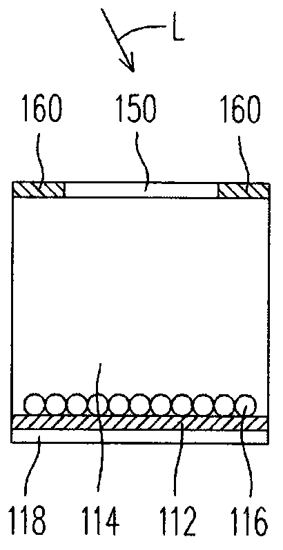
图1绘示为本发明的一实施例的电泳显示像素的俯视示意图,而图2绘示为图1的电泳显示像素沿剖线A-A’所绘示的剖面示意图。请同时参照图1与图2,电泳显示像素100包括电泳显示薄膜110、基板120、第一主动元件130、第二主动元件140、第一电极150以及第二电极160。基板120配置于电泳显示薄膜110上,并具有透光区122以及非透光区124。第一主动元件130以及第二主动元件140皆配置于基板120上并位于非透光区124中。第一电极150配置于基板120上,位于透光区122中,并电性连接第一主动元件130,而第二电极160则配置于基板120上,位于非透光区124中,并电性连接第二主动元件140。FIG. 1 is a schematic top view of an electrophoretic display pixel according to an embodiment of the present invention, and FIG. 2 is a schematic cross-sectional view of the electrophoretic display pixel of FIG. 1 along the section line A-A'. Please refer to FIG. 1 and FIG. 2 at the same time. The
具体而言,电泳显示薄膜110具有电极层112、显示基质114以及多个显示粒子116。显示粒子116分布于显示基质114中,且电极层112与基板120位于显示基质114的相对两侧。以本实施例而言,光线L穿透透光区122而进入电泳显示薄膜110而后被反射出来以进行显示,所以基板120所在的一侧为显示侧。Specifically, the
换言之,使用者在使用具有电泳显示像素100的电子装置时,是位于光线L所在的一侧,且使用者沿光线L的入射方向观看画面的。因此,第一电极150与第二电极160的材质例如是透明导电材质。为了提升显示品质,电泳显示像素100例如更包括吸光层118,其配置于电泳显示薄膜110远离基板120的一侧。In other words, when using the electronic device with the
图3A至图3C绘示为图1与图2所示的电泳显示像素进行显示的三种状态示意图,其中图3A至图3C仅简要地绘示出显示薄膜、第一电极以及第二电极。请参照图3A至图3C,显示粒子116一般是带有正电荷或负电荷的粒子,所以显示粒子116的移动例如可由电极层112、第一电极150与第二电极160的电场控制。3A to 3C are schematic diagrams showing three states of the electrophoretic display pixels shown in FIG. 1 and FIG. 2 , wherein FIG. 3A to FIG. 3C only briefly show the display film, the first electrode and the second electrode. Referring to FIGS. 3A to 3C , the
如图3A所示,在状态I时,假设显示粒子116带正电荷,电极层112被施予负电压,而第一电极150与第二电极160被施予正电压。所以,依据电场的方向及分布,显示粒子116会朝向电极层112移动而接近电极层112的表面。此时,光线L会先穿过显示基质114而后被显示粒子116反射。所以在状态I时,使用者沿光线L的入射方向观看,可看到电泳显示像素100呈现显示基质114的颜色。若显示基质114为红色,则电泳显示像素100在状态I下呈现红色的画面。当然,显示基质114的颜色可以随不同的设计而变。As shown in FIG. 3A , in state I, assuming that the
如图3B所示,在状态II时,假设显示粒子116带正电荷,电极层112被施予正电压,而第一电极150以及第二电极160被施予负电压。所以,依据电场的方向及分布,显示粒子116的移动方向会趋向第一电极150以及第二电极160的表面。此时,光线L直接被显示粒子116反射而显示显示粒子116的颜色。若显示粒子116为白色,在状态II下,使用者沿光线L的入射方向观看,可看到电泳显示像素100显示白色画面。同样地,随显示粒子116的颜色不同,电泳显示像素100在状态II显示的画面颜色也不同。换言之,在状态II下,使用者会看到显示粒子116所呈现的颜色。As shown in FIG. 3B , in state II, assuming that the
如图3C所示,在状态III时,假设显示粒子116带正电荷,电极层112与第一电极150被施予正电压,而仅有第二电极160被施予负电压。依据电场的方向及分布,带正电荷的显示粒子116会移动至第二电极160所在区域中。也就是说,本实施例的显示粒子116除了可以进行纵向的位移之外,还可通过第一电极150与第二电极160的电场变化来控制显示粒子116的横向位移。As shown in FIG. 3C , in state III, assuming that the
由图1、图2与图3A-图3C可知,第二电极160所在位置为非透光区124,所以在图3C所示的状态III下光线L不会被显示粒子116反射而被吸光层118吸收。所以,使用者由基板120的一侧朝向电泳显示薄膜110观看时,光线L不会被反射出来而可看到电泳显示像素100呈现黑色的画面。值得一提的是,本实施例的第二电极160所在位置无法透光,所以光线L在在图3C所示的状态III下不易入射至显示粒子116,也不易被反射出去。如此一来,电泳显示像素100在显示黑色画面时不容易产生反射光而可以呈现出较黑的黑色画面。通过这样的设计,电泳显示像素100即具有相当高的显示对比度。From FIG. 1, FIG. 2 and FIG. 3A-FIG. 3C, it can be seen that the position of the
具体来说,请继续参照图1与图2,电泳显示像素100更包括二扫描线182、184以及一数据线190。第一主动元件130电性连接扫描线182,而第二主动元件140电性连接扫描线184,且第一主动元件130以及第二主动元件140电性连接同样的数据线190。本实施例的第一主动元件130与第二主动元件140分别连接至扫描线182与扫描线184。所以,第一电极150与第二电极160可具有不同的电压以控制显示粒子116的横向位移。Specifically, please continue to refer to FIG. 1 and FIG. 2 , the
在本实施例中,第一主动元件130以及第二主动元件140分别包括一栅极G、一源极S以及一漏极D。源极S与漏极D分别位于栅极G的两侧,且第一电极150电性连接第一主动元件130的漏极D,而第二电极160电性连接第二主动元件140的漏极D。第一主动元件130以及第二主动元件140实质上为薄膜晶体管。栅极G、源极S以及漏极D的材质例如为一非透光导电材质。In this embodiment, the first
另外,电泳显示像素100更包括电容电极170,其配置于基板120上并位于非透光区124中。第一主动元件130的漏极D以及第二主动元件140的漏极D分别地与电容电极170重叠以构成对应的储存电容。储存电容的设计有助于维持电泳显示像素100的显示稳定性。此外,电容电极170的材质也例如为一非透光导电材质。In addition, the
扫描线182、184、数据线190、第一主动元件130、第二主动元件140以及电容电极170都是不透光元件。因此,本实施例的非透光区124可说是由这些不透光元件所在位置定义出来的。这些不透光元件配置于显示侧(也就是基板120所在的一侧,也就是接近使用者的一侧)。所以,本实施例的电泳显示像素100可以借着这些不透光元件遮蔽不必要的漏光或是阻挡光线L被非透光区124中的显示粒子116反射因而提升电泳显示像素100的显示对比。The
进一步而言,本实施例的电泳显示像素100不需要配置额外的遮光元件就可以有效地提高显示品质。因此,本实施例的电泳显示像素100可采用既有的工艺来制作,不会造成工艺步骤的复杂化。另外,本发明不限定位于非透光区124中的元件为何种元件,这些元件可包括薄膜晶体管元件、储存电容等至少包括一非透光层以阻挡或降低光线的穿透的元件。Furthermore, the
详细而言,电泳显示像素100的制作方式例如是先将扫描线182、184、数据线190、第一主动元件130、第二主动元件140、第一电极150、第二电极160以及电容电极170等元件利用薄膜沉积工艺以及光刻工艺等可应用于主动元件阵列的制作方式制作于基板120上。接着,再将基板120配置有上述元件的一侧与电泳显示薄膜110组装或是贴附在一起。换言之,电泳显示像素100的制作方式与以往的电泳显示器的制作方式大致相同。In detail, the manufacturing method of the
由于电泳显示像素100的组成元件与公知电泳显示器的组成元件皆相同,本实施例的设计可在不改变组成元件的前提下完成高显示对比的设计。所以,本实施例的设计并不会造成工艺上的复杂化或是加重工艺的成本。在此,电泳显示像素100例如可以应用于电子纸显示器或可挠性显示器中。Since the components of the
图4绘示为本发明的另一实施例的电泳显示像素的部分构件的俯视示意图,其中图4省略了电泳显示薄膜与基板。请参照图4,另一种电泳显示像素200中,第一主动元件130与第二主动元件140由一条扫描线280以及两条数据线292、294所驱动。第一主动元件130以及第二主动元件140电性连接同一条扫描线280。此外,第一主动元件130电性连接数据线292,而第二主动元件140电性连接数据线294。FIG. 4 is a schematic top view of some components of an electrophoretic display pixel according to another embodiment of the present invention, wherein the electrophoretic display film and the substrate are omitted in FIG. 4 . Referring to FIG. 4 , in another
本实施例通过不同的数据线292、294传输对应的信号至第一电极150与第二电极160。所以,第一电极150与第二电极160的极性各自由独立的信号决定以控制显示薄膜(未绘示)中的显示粒子(未绘示)的移动方向及位置。另外,本实施例的设计与前述实施例都是将第一主动元件130、第二主动元件140、电容电极170等不透光元件的所在位置定义为非透光区。并且,第二电极160都是位于非透光区中。所以,显示黑色画面时,只需将显示粒子(未绘示)吸引至第二电极160所在位置就不容易反射光线。也就是说,电泳显示像素200可以显示较黑的黑色画面而具有较高的显示对比。In this embodiment, corresponding signals are transmitted to the
相似地,本实施例的设计主要在于将不透光的元件设置于接近使用者的显示侧。所以,本实施例的电泳显示像素200显示黑色画面时,可以利用既有的不透光元件遮蔽显示粒子(未绘示)。如此一来,电泳显示像素200显示的黑色画面足够黑而达到高显示对比的显示效果。Similarly, the design of this embodiment mainly lies in disposing the opaque element on the display side close to the user. Therefore, when the
综上所述,本发明将主动元件所配置的基板设置为显示侧。所以,主动元件及电容电极等具有不透光性质的元件可以在基板上定义出非透光区。本发明在透光区与非透光区中分别配置第一电极与第二电极以控制显示粒子的横向移动。显示粒子横向移动至第二电极所在区域时,显示粒子会被不透光元件遮蔽无法反射光线而可显示较黑的黑色画面。所以,本发明的电泳显示像素以及显示装置具有相当不错的显示对比。在这样的设计下,电泳显示像素的组成元件及制作方法都不需有大幅的改变,也就是说,本发明可以在既有的组成元件设计下达到高显示对比的显示效果。To sum up, in the present invention, the substrate on which the active components are configured is set as the display side. Therefore, components with opaque properties such as active components and capacitive electrodes can define opaque regions on the substrate. In the present invention, the first electrode and the second electrode are arranged respectively in the light-transmitting area and the non-light-transmitting area to control the lateral movement of the display particles. When the display particles move laterally to the area where the second electrode is located, the display particles will be blocked by the opaque element and cannot reflect light, so a darker black picture can be displayed. Therefore, the electrophoretic display pixel and the display device of the present invention have quite good display contrast. Under such a design, there is no need to greatly change the components and manufacturing method of the electrophoretic display pixel, that is to say, the present invention can achieve a high display contrast display effect under the existing component component design.
当然,本发明还可有其它多种实施例,在不背离本发明精神及其实质的情况下,熟悉本领域的技术人员当可根据本发明作出各种相应的改变和变形,但这些相应的改变和变形都应属于本发明所附的权利要求的保护范围。Certainly, the present invention also can have other multiple embodiments, without departing from the spirit and essence of the present invention, those skilled in the art can make various corresponding changes and deformations according to the present invention, but these corresponding Changes and deformations should belong to the scope of protection of the appended claims of the present invention.
Claims (12)
Priority Applications (1)
| Application Number | Priority Date | Filing Date | Title |
|---|---|---|---|
| CN2009102118878A CN101699343B (en) | 2009-11-09 | 2009-11-09 | Electrophoretic display pixel and display device |
Applications Claiming Priority (1)
| Application Number | Priority Date | Filing Date | Title |
|---|---|---|---|
| CN2009102118878A CN101699343B (en) | 2009-11-09 | 2009-11-09 | Electrophoretic display pixel and display device |
Publications (2)
| Publication Number | Publication Date |
|---|---|
| CN101699343A CN101699343A (en) | 2010-04-28 |
| CN101699343B true CN101699343B (en) | 2012-01-25 |
Family
ID=42147805
Family Applications (1)
| Application Number | Title | Priority Date | Filing Date |
|---|---|---|---|
| CN2009102118878A Active CN101699343B (en) | 2009-11-09 | 2009-11-09 | Electrophoretic display pixel and display device |
Country Status (1)
| Country | Link |
|---|---|
| CN (1) | CN101699343B (en) |
Families Citing this family (1)
| Publication number | Priority date | Publication date | Assignee | Title |
|---|---|---|---|---|
| WO2024146447A1 (en) * | 2023-01-03 | 2024-07-11 | 京东方科技集团股份有限公司 | Reflective display panel, manufacturing method and driving method therefor, and display apparatus |
Citations (3)
| Publication number | Priority date | Publication date | Assignee | Title |
|---|---|---|---|---|
| CN1908794A (en) * | 2005-08-01 | 2007-02-07 | Nec液晶技术株式会社 | Color electronic paper display device |
| CN101093335A (en) * | 2006-06-22 | 2007-12-26 | 三星电子株式会社 | Electrophoretic display and manufacturing method thereof |
| CN101169567A (en) * | 2006-10-25 | 2008-04-30 | 精工爱普生株式会社 | Electro-optical devices and electronic devices |
-
2009
- 2009-11-09 CN CN2009102118878A patent/CN101699343B/en active Active
Patent Citations (3)
| Publication number | Priority date | Publication date | Assignee | Title |
|---|---|---|---|---|
| CN1908794A (en) * | 2005-08-01 | 2007-02-07 | Nec液晶技术株式会社 | Color electronic paper display device |
| CN101093335A (en) * | 2006-06-22 | 2007-12-26 | 三星电子株式会社 | Electrophoretic display and manufacturing method thereof |
| CN101169567A (en) * | 2006-10-25 | 2008-04-30 | 精工爱普生株式会社 | Electro-optical devices and electronic devices |
Also Published As
| Publication number | Publication date |
|---|---|
| CN101699343A (en) | 2010-04-28 |
Similar Documents
| Publication | Publication Date | Title |
|---|---|---|
| CN102540528B (en) | Display panel and driving method thereof | |
| KR101880421B1 (en) | Electric field driving display device | |
| US9285647B2 (en) | TFT array substrate, E-paper display panel and method for manufacturing the same | |
| US20120105337A1 (en) | Liquid crystal display with built-in touch screen panel | |
| US8228309B2 (en) | Display apparatus and information input apparatus | |
| TWI399602B (en) | Liquid crystal display device and electronic apparatus | |
| US8208098B2 (en) | Organic light emitting diode display and driving method thereof | |
| US20140022465A1 (en) | Color filter substrate, touch display panel and touch display device | |
| US9865621B2 (en) | Display device | |
| CN104678629B (en) | Display panel | |
| US8009237B2 (en) | Display substrate, method for manufacturing the same, and display panel having the same | |
| KR100964761B1 (en) | Liquid crystal display | |
| US20050200793A1 (en) | In-plane switching mode liquid crystal display device and method of fabricating the same | |
| CN110554530A (en) | Display panel and display device | |
| US8212973B2 (en) | Color filter substrate and liquid crystal display | |
| JP2011043720A (en) | Electrophoretic display element | |
| US20180136785A1 (en) | Position input device and display device having position input function | |
| US10571753B2 (en) | Liquid crystal panel | |
| CN101699343B (en) | Electrophoretic display pixel and display device | |
| US9147371B2 (en) | Liquid crystal display panel used in normally black mode and display apparatus using the same | |
| CN102809861A (en) | Pixel structure of liquid crystal display device | |
| CN102375276B (en) | LCD panel | |
| CN101738779B (en) | Liquid crystal display and its color filter substrate | |
| TWI391715B (en) | Color filter substrate and liquid crystal display | |
| CN100412670C (en) | Pixel structure and liquid crystal display panel |
Legal Events
| Date | Code | Title | Description |
|---|---|---|---|
| C06 | Publication | ||
| PB01 | Publication | ||
| C10 | Entry into substantive examination | ||
| SE01 | Entry into force of request for substantive examination | ||
| C14 | Grant of patent or utility model | ||
| GR01 | Patent grant |