CN101438191A - Light redirecting film having surface nano-nodules - Google Patents
Light redirecting film having surface nano-nodules Download PDFInfo
- Publication number
- CN101438191A CN101438191A CNA2007800159321A CN200780015932A CN101438191A CN 101438191 A CN101438191 A CN 101438191A CN A2007800159321 A CNA2007800159321 A CN A2007800159321A CN 200780015932 A CN200780015932 A CN 200780015932A CN 101438191 A CN101438191 A CN 101438191A
- Authority
- CN
- China
- Prior art keywords
- macrostructure
- nodules
- light
- nano
- film
- Prior art date
- Legal status (The legal status is an assumption and is not a legal conclusion. Google has not performed a legal analysis and makes no representation as to the accuracy of the status listed.)
- Pending
Links
- 230000003287 optical effect Effects 0.000 claims abstract description 68
- 230000005540 biological transmission Effects 0.000 claims description 18
- 239000000126 substance Substances 0.000 claims description 15
- 229910052751 metal Inorganic materials 0.000 claims description 13
- 239000002184 metal Substances 0.000 claims description 13
- 238000000034 method Methods 0.000 claims description 10
- 238000004519 manufacturing process Methods 0.000 claims description 8
- 238000007747 plating Methods 0.000 claims description 8
- 239000011248 coating agent Substances 0.000 claims description 7
- 238000000576 coating method Methods 0.000 claims description 7
- 239000012528 membrane Substances 0.000 claims description 7
- 230000010354 integration Effects 0.000 claims 2
- 235000019994 cava Nutrition 0.000 claims 1
- 239000010408 film Substances 0.000 description 124
- 239000004973 liquid crystal related substance Substances 0.000 description 23
- 239000000463 material Substances 0.000 description 22
- 230000000007 visual effect Effects 0.000 description 22
- 229920000642 polymer Polymers 0.000 description 16
- VYZAMTAEIAYCRO-UHFFFAOYSA-N Chromium Chemical compound [Cr] VYZAMTAEIAYCRO-UHFFFAOYSA-N 0.000 description 14
- 229910052804 chromium Inorganic materials 0.000 description 12
- 239000011651 chromium Substances 0.000 description 12
- 238000009826 distribution Methods 0.000 description 12
- 230000008859 change Effects 0.000 description 11
- 230000014509 gene expression Effects 0.000 description 11
- 238000009792 diffusion process Methods 0.000 description 10
- 239000004372 Polyvinyl alcohol Substances 0.000 description 8
- 230000000694 effects Effects 0.000 description 8
- 238000000265 homogenisation Methods 0.000 description 8
- 230000010287 polarization Effects 0.000 description 8
- 229920002451 polyvinyl alcohol Polymers 0.000 description 8
- PXHVJJICTQNCMI-UHFFFAOYSA-N Nickel Chemical compound [Ni] PXHVJJICTQNCMI-UHFFFAOYSA-N 0.000 description 6
- 238000005516 engineering process Methods 0.000 description 6
- 238000005286 illumination Methods 0.000 description 6
- 230000003321 amplification Effects 0.000 description 5
- 238000005452 bending Methods 0.000 description 5
- 230000008901 benefit Effects 0.000 description 5
- 210000002858 crystal cell Anatomy 0.000 description 5
- 230000001976 improved effect Effects 0.000 description 5
- 239000011159 matrix material Substances 0.000 description 5
- 238000003199 nucleic acid amplification method Methods 0.000 description 5
- 239000013307 optical fiber Substances 0.000 description 5
- 238000002834 transmittance Methods 0.000 description 5
- 229920002284 Cellulose triacetate Polymers 0.000 description 4
- 239000004988 Nematic liquid crystal Substances 0.000 description 4
- NNLVGZFZQQXQNW-ADJNRHBOSA-N [(2r,3r,4s,5r,6s)-4,5-diacetyloxy-3-[(2s,3r,4s,5r,6r)-3,4,5-triacetyloxy-6-(acetyloxymethyl)oxan-2-yl]oxy-6-[(2r,3r,4s,5r,6s)-4,5,6-triacetyloxy-2-(acetyloxymethyl)oxan-3-yl]oxyoxan-2-yl]methyl acetate Chemical compound O([C@@H]1O[C@@H]([C@H]([C@H](OC(C)=O)[C@H]1OC(C)=O)O[C@H]1[C@@H]([C@@H](OC(C)=O)[C@H](OC(C)=O)[C@@H](COC(C)=O)O1)OC(C)=O)COC(=O)C)[C@@H]1[C@@H](COC(C)=O)O[C@@H](OC(C)=O)[C@H](OC(C)=O)[C@H]1OC(C)=O NNLVGZFZQQXQNW-ADJNRHBOSA-N 0.000 description 4
- 230000015572 biosynthetic process Effects 0.000 description 4
- 238000000151 deposition Methods 0.000 description 4
- 230000008021 deposition Effects 0.000 description 4
- 238000005755 formation reaction Methods 0.000 description 4
- 230000008569 process Effects 0.000 description 4
- 239000000758 substrate Substances 0.000 description 4
- PNEYBMLMFCGWSK-UHFFFAOYSA-N Alumina Chemical compound [O-2].[O-2].[O-2].[Al+3].[Al+3] PNEYBMLMFCGWSK-UHFFFAOYSA-N 0.000 description 3
- 239000010953 base metal Substances 0.000 description 3
- 239000011324 bead Substances 0.000 description 3
- 230000008878 coupling Effects 0.000 description 3
- 238000010168 coupling process Methods 0.000 description 3
- 238000005859 coupling reaction Methods 0.000 description 3
- 238000013461 design Methods 0.000 description 3
- 235000019589 hardness Nutrition 0.000 description 3
- 238000003754 machining Methods 0.000 description 3
- 238000005259 measurement Methods 0.000 description 3
- 229910052759 nickel Inorganic materials 0.000 description 3
- VYPSYNLAJGMNEJ-UHFFFAOYSA-N Silicium dioxide Chemical compound O=[Si]=O VYPSYNLAJGMNEJ-UHFFFAOYSA-N 0.000 description 2
- GWEVSGVZZGPLCZ-UHFFFAOYSA-N Titan oxide Chemical compound O=[Ti]=O GWEVSGVZZGPLCZ-UHFFFAOYSA-N 0.000 description 2
- 238000010521 absorption reaction Methods 0.000 description 2
- 238000009825 accumulation Methods 0.000 description 2
- 229910045601 alloy Inorganic materials 0.000 description 2
- 239000000956 alloy Substances 0.000 description 2
- 238000000149 argon plasma sintering Methods 0.000 description 2
- 238000005260 corrosion Methods 0.000 description 2
- 230000007547 defect Effects 0.000 description 2
- 239000005262 ferroelectric liquid crystals (FLCs) Substances 0.000 description 2
- 239000000835 fiber Substances 0.000 description 2
- 230000004807 localization Effects 0.000 description 2
- 230000000116 mitigating effect Effects 0.000 description 2
- 239000000203 mixture Substances 0.000 description 2
- 239000002105 nanoparticle Substances 0.000 description 2
- 229920000515 polycarbonate Polymers 0.000 description 2
- 239000004417 polycarbonate Substances 0.000 description 2
- 229920000728 polyester Polymers 0.000 description 2
- 229920000098 polyolefin Polymers 0.000 description 2
- 230000009467 reduction Effects 0.000 description 2
- 230000003252 repetitive effect Effects 0.000 description 2
- 239000007921 spray Substances 0.000 description 2
- 235000019587 texture Nutrition 0.000 description 2
- RICKKZXCGCSLIU-UHFFFAOYSA-N 2-[2-[carboxymethyl-[[3-hydroxy-5-(hydroxymethyl)-2-methylpyridin-4-yl]methyl]amino]ethyl-[[3-hydroxy-5-(hydroxymethyl)-2-methylpyridin-4-yl]methyl]amino]acetic acid Chemical compound CC1=NC=C(CO)C(CN(CCN(CC(O)=O)CC=2C(=C(C)N=CC=2CO)O)CC(O)=O)=C1O RICKKZXCGCSLIU-UHFFFAOYSA-N 0.000 description 1
- BSYNRYMUTXBXSQ-UHFFFAOYSA-N Aspirin Chemical compound CC(=O)OC1=CC=CC=C1C(O)=O BSYNRYMUTXBXSQ-UHFFFAOYSA-N 0.000 description 1
- BVKZGUZCCUSVTD-UHFFFAOYSA-L Carbonate Chemical compound [O-]C([O-])=O BVKZGUZCCUSVTD-UHFFFAOYSA-L 0.000 description 1
- 229920000089 Cyclic olefin copolymer Polymers 0.000 description 1
- CWYNVVGOOAEACU-UHFFFAOYSA-N Fe2+ Chemical compound [Fe+2] CWYNVVGOOAEACU-UHFFFAOYSA-N 0.000 description 1
- KRHYYFGTRYWZRS-UHFFFAOYSA-M Fluoride anion Chemical compound [F-] KRHYYFGTRYWZRS-UHFFFAOYSA-M 0.000 description 1
- 229910000760 Hardened steel Inorganic materials 0.000 description 1
- 208000037656 Respiratory Sounds Diseases 0.000 description 1
- 150000001336 alkenes Chemical group 0.000 description 1
- 230000000573 anti-seizure effect Effects 0.000 description 1
- 210000003050 axon Anatomy 0.000 description 1
- 230000009286 beneficial effect Effects 0.000 description 1
- 238000005422 blasting Methods 0.000 description 1
- 238000005266 casting Methods 0.000 description 1
- 238000006243 chemical reaction Methods 0.000 description 1
- 230000000052 comparative effect Effects 0.000 description 1
- 230000008602 contraction Effects 0.000 description 1
- 229920001577 copolymer Polymers 0.000 description 1
- 230000007797 corrosion Effects 0.000 description 1
- 150000001925 cycloalkenes Chemical class 0.000 description 1
- 230000002950 deficient Effects 0.000 description 1
- 238000007516 diamond turning Methods 0.000 description 1
- 230000003292 diminished effect Effects 0.000 description 1
- 238000006073 displacement reaction Methods 0.000 description 1
- 230000005611 electricity Effects 0.000 description 1
- 238000004070 electrodeposition Methods 0.000 description 1
- 238000007772 electroless plating Methods 0.000 description 1
- 230000008030 elimination Effects 0.000 description 1
- 238000003379 elimination reaction Methods 0.000 description 1
- 238000005265 energy consumption Methods 0.000 description 1
- 150000002148 esters Chemical class 0.000 description 1
- -1 ferrous metals Chemical class 0.000 description 1
- 230000004927 fusion Effects 0.000 description 1
- 239000005337 ground glass Substances 0.000 description 1
- 229920001519 homopolymer Polymers 0.000 description 1
- 229910052739 hydrogen Inorganic materials 0.000 description 1
- 239000001257 hydrogen Substances 0.000 description 1
- 125000004435 hydrogen atom Chemical class [H]* 0.000 description 1
- 238000007373 indentation Methods 0.000 description 1
- 229910003437 indium oxide Inorganic materials 0.000 description 1
- PJXISJQVUVHSOJ-UHFFFAOYSA-N indium(iii) oxide Chemical compound [O-2].[O-2].[O-2].[In+3].[In+3] PJXISJQVUVHSOJ-UHFFFAOYSA-N 0.000 description 1
- 230000001939 inductive effect Effects 0.000 description 1
- 229910010272 inorganic material Inorganic materials 0.000 description 1
- 239000011147 inorganic material Substances 0.000 description 1
- 230000003993 interaction Effects 0.000 description 1
- PNDPGZBMCMUPRI-UHFFFAOYSA-N iodine Chemical compound II PNDPGZBMCMUPRI-UHFFFAOYSA-N 0.000 description 1
- 230000001788 irregular Effects 0.000 description 1
- 230000031700 light absorption Effects 0.000 description 1
- 239000000155 melt Substances 0.000 description 1
- 238000012544 monitoring process Methods 0.000 description 1
- 239000012788 optical film Substances 0.000 description 1
- 239000002245 particle Substances 0.000 description 1
- 230000000737 periodic effect Effects 0.000 description 1
- 239000002985 plastic film Substances 0.000 description 1
- 229920000058 polyacrylate Polymers 0.000 description 1
- 229920006254 polymer film Polymers 0.000 description 1
- 238000012545 processing Methods 0.000 description 1
- 230000002035 prolonged effect Effects 0.000 description 1
- 238000012797 qualification Methods 0.000 description 1
- 230000005855 radiation Effects 0.000 description 1
- 230000001105 regulatory effect Effects 0.000 description 1
- 230000002040 relaxant effect Effects 0.000 description 1
- 230000004044 response Effects 0.000 description 1
- 239000000377 silicon dioxide Substances 0.000 description 1
- 235000012239 silicon dioxide Nutrition 0.000 description 1
- 238000005507 spraying Methods 0.000 description 1
- 230000008093 supporting effect Effects 0.000 description 1
- 238000001356 surgical procedure Methods 0.000 description 1
- 239000010409 thin film Substances 0.000 description 1
Images


Classifications
-
- G—PHYSICS
- G02—OPTICS
- G02B—OPTICAL ELEMENTS, SYSTEMS OR APPARATUS
- G02B6/00—Light guides; Structural details of arrangements comprising light guides and other optical elements, e.g. couplings
- G02B6/0001—Light guides; Structural details of arrangements comprising light guides and other optical elements, e.g. couplings specially adapted for lighting devices or systems
- G02B6/0011—Light guides; Structural details of arrangements comprising light guides and other optical elements, e.g. couplings specially adapted for lighting devices or systems the light guides being planar or of plate-like form
- G02B6/0033—Means for improving the coupling-out of light from the light guide
- G02B6/005—Means for improving the coupling-out of light from the light guide provided by one optical element, or plurality thereof, placed on the light output side of the light guide
- G02B6/0053—Prismatic sheet or layer; Brightness enhancement element, sheet or layer
-
- G—PHYSICS
- G02—OPTICS
- G02B—OPTICAL ELEMENTS, SYSTEMS OR APPARATUS
- G02B5/00—Optical elements other than lenses
- G02B5/04—Prisms
-
- B—PERFORMING OPERATIONS; TRANSPORTING
- B29—WORKING OF PLASTICS; WORKING OF SUBSTANCES IN A PLASTIC STATE IN GENERAL
- B29C—SHAPING OR JOINING OF PLASTICS; SHAPING OF MATERIAL IN A PLASTIC STATE, NOT OTHERWISE PROVIDED FOR; AFTER-TREATMENT OF THE SHAPED PRODUCTS, e.g. REPAIRING
- B29C43/00—Compression moulding, i.e. applying external pressure to flow the moulding material; Apparatus therefor
- B29C43/22—Compression moulding, i.e. applying external pressure to flow the moulding material; Apparatus therefor of articles of indefinite length
- B29C43/222—Compression moulding, i.e. applying external pressure to flow the moulding material; Apparatus therefor of articles of indefinite length characterised by the shape of the surface
-
- B—PERFORMING OPERATIONS; TRANSPORTING
- B29—WORKING OF PLASTICS; WORKING OF SUBSTANCES IN A PLASTIC STATE IN GENERAL
- B29C—SHAPING OR JOINING OF PLASTICS; SHAPING OF MATERIAL IN A PLASTIC STATE, NOT OTHERWISE PROVIDED FOR; AFTER-TREATMENT OF THE SHAPED PRODUCTS, e.g. REPAIRING
- B29C43/00—Compression moulding, i.e. applying external pressure to flow the moulding material; Apparatus therefor
- B29C43/22—Compression moulding, i.e. applying external pressure to flow the moulding material; Apparatus therefor of articles of indefinite length
- B29C43/24—Calendering
-
- B—PERFORMING OPERATIONS; TRANSPORTING
- B29—WORKING OF PLASTICS; WORKING OF SUBSTANCES IN A PLASTIC STATE IN GENERAL
- B29C—SHAPING OR JOINING OF PLASTICS; SHAPING OF MATERIAL IN A PLASTIC STATE, NOT OTHERWISE PROVIDED FOR; AFTER-TREATMENT OF THE SHAPED PRODUCTS, e.g. REPAIRING
- B29C43/00—Compression moulding, i.e. applying external pressure to flow the moulding material; Apparatus therefor
- B29C43/22—Compression moulding, i.e. applying external pressure to flow the moulding material; Apparatus therefor of articles of indefinite length
- B29C43/28—Compression moulding, i.e. applying external pressure to flow the moulding material; Apparatus therefor of articles of indefinite length incorporating preformed parts or layers, e.g. compression moulding around inserts or for coating articles
-
- B—PERFORMING OPERATIONS; TRANSPORTING
- B29—WORKING OF PLASTICS; WORKING OF SUBSTANCES IN A PLASTIC STATE IN GENERAL
- B29C—SHAPING OR JOINING OF PLASTICS; SHAPING OF MATERIAL IN A PLASTIC STATE, NOT OTHERWISE PROVIDED FOR; AFTER-TREATMENT OF THE SHAPED PRODUCTS, e.g. REPAIRING
- B29C59/00—Surface shaping of articles, e.g. embossing; Apparatus therefor
- B29C59/02—Surface shaping of articles, e.g. embossing; Apparatus therefor by mechanical means, e.g. pressing
- B29C59/04—Surface shaping of articles, e.g. embossing; Apparatus therefor by mechanical means, e.g. pressing using rollers or endless belts
- B29C59/046—Surface shaping of articles, e.g. embossing; Apparatus therefor by mechanical means, e.g. pressing using rollers or endless belts for layered or coated substantially flat surfaces
-
- G—PHYSICS
- G02—OPTICS
- G02B—OPTICAL ELEMENTS, SYSTEMS OR APPARATUS
- G02B5/00—Optical elements other than lenses
- G02B5/02—Diffusing elements; Afocal elements
- G02B5/0205—Diffusing elements; Afocal elements characterised by the diffusing properties
- G02B5/021—Diffusing elements; Afocal elements characterised by the diffusing properties the diffusion taking place at the element's surface, e.g. by means of surface roughening or microprismatic structures
- G02B5/0221—Diffusing elements; Afocal elements characterised by the diffusing properties the diffusion taking place at the element's surface, e.g. by means of surface roughening or microprismatic structures the surface having an irregular structure
-
- G—PHYSICS
- G02—OPTICS
- G02B—OPTICAL ELEMENTS, SYSTEMS OR APPARATUS
- G02B5/00—Optical elements other than lenses
- G02B5/02—Diffusing elements; Afocal elements
- G02B5/0268—Diffusing elements; Afocal elements characterized by the fabrication or manufacturing method
-
- G—PHYSICS
- G02—OPTICS
- G02B—OPTICAL ELEMENTS, SYSTEMS OR APPARATUS
- G02B5/00—Optical elements other than lenses
- G02B5/02—Diffusing elements; Afocal elements
- G02B5/0273—Diffusing elements; Afocal elements characterized by the use
- G02B5/0278—Diffusing elements; Afocal elements characterized by the use used in transmission
-
- G—PHYSICS
- G02—OPTICS
- G02B—OPTICAL ELEMENTS, SYSTEMS OR APPARATUS
- G02B5/00—Optical elements other than lenses
- G02B5/02—Diffusing elements; Afocal elements
- G02B5/0273—Diffusing elements; Afocal elements characterized by the use
- G02B5/0284—Diffusing elements; Afocal elements characterized by the use used in reflection
-
- G—PHYSICS
- G02—OPTICS
- G02B—OPTICAL ELEMENTS, SYSTEMS OR APPARATUS
- G02B6/00—Light guides; Structural details of arrangements comprising light guides and other optical elements, e.g. couplings
- G02B6/0001—Light guides; Structural details of arrangements comprising light guides and other optical elements, e.g. couplings specially adapted for lighting devices or systems
- G02B6/0011—Light guides; Structural details of arrangements comprising light guides and other optical elements, e.g. couplings specially adapted for lighting devices or systems the light guides being planar or of plate-like form
- G02B6/0065—Manufacturing aspects; Material aspects
-
- G—PHYSICS
- G02—OPTICS
- G02F—OPTICAL DEVICES OR ARRANGEMENTS FOR THE CONTROL OF LIGHT BY MODIFICATION OF THE OPTICAL PROPERTIES OF THE MEDIA OF THE ELEMENTS INVOLVED THEREIN; NON-LINEAR OPTICS; FREQUENCY-CHANGING OF LIGHT; OPTICAL LOGIC ELEMENTS; OPTICAL ANALOGUE/DIGITAL CONVERTERS
- G02F1/00—Devices or arrangements for the control of the intensity, colour, phase, polarisation or direction of light arriving from an independent light source, e.g. switching, gating or modulating; Non-linear optics
- G02F1/01—Devices or arrangements for the control of the intensity, colour, phase, polarisation or direction of light arriving from an independent light source, e.g. switching, gating or modulating; Non-linear optics for the control of the intensity, phase, polarisation or colour
- G02F1/13—Devices or arrangements for the control of the intensity, colour, phase, polarisation or direction of light arriving from an independent light source, e.g. switching, gating or modulating; Non-linear optics for the control of the intensity, phase, polarisation or colour based on liquid crystals, e.g. single liquid crystal display cells
- G02F1/133—Constructional arrangements; Operation of liquid crystal cells; Circuit arrangements
- G02F1/1333—Constructional arrangements; Manufacturing methods
- G02F1/1335—Structural association of cells with optical devices, e.g. polarisers or reflectors
-
- B—PERFORMING OPERATIONS; TRANSPORTING
- B29—WORKING OF PLASTICS; WORKING OF SUBSTANCES IN A PLASTIC STATE IN GENERAL
- B29C—SHAPING OR JOINING OF PLASTICS; SHAPING OF MATERIAL IN A PLASTIC STATE, NOT OTHERWISE PROVIDED FOR; AFTER-TREATMENT OF THE SHAPED PRODUCTS, e.g. REPAIRING
- B29C59/00—Surface shaping of articles, e.g. embossing; Apparatus therefor
- B29C59/02—Surface shaping of articles, e.g. embossing; Apparatus therefor by mechanical means, e.g. pressing
- B29C59/022—Surface shaping of articles, e.g. embossing; Apparatus therefor by mechanical means, e.g. pressing characterised by the disposition or the configuration, e.g. dimensions, of the embossments or the shaping tools therefor
- B29C2059/023—Microembossing
-
- B—PERFORMING OPERATIONS; TRANSPORTING
- B82—NANOTECHNOLOGY
- B82Y—SPECIFIC USES OR APPLICATIONS OF NANOSTRUCTURES; MEASUREMENT OR ANALYSIS OF NANOSTRUCTURES; MANUFACTURE OR TREATMENT OF NANOSTRUCTURES
- B82Y30/00—Nanotechnology for materials or surface science, e.g. nanocomposites
-
- C—CHEMISTRY; METALLURGY
- C09—DYES; PAINTS; POLISHES; NATURAL RESINS; ADHESIVES; COMPOSITIONS NOT OTHERWISE PROVIDED FOR; APPLICATIONS OF MATERIALS NOT OTHERWISE PROVIDED FOR
- C09K—MATERIALS FOR MISCELLANEOUS APPLICATIONS, NOT PROVIDED FOR ELSEWHERE
- C09K2323/00—Functional layers of liquid crystal optical display excluding electroactive liquid crystal layer characterised by chemical composition
Abstract
A light redirecting optical device comprises a polymeric film containing a light entry and a light exit surface and bearing on the light exit surface convex macrostructures that have a length, diameter, or other major dimension of at least 25 micrometers, wherein a major portion of the macrostructure surfaces is covered with nano-nodules having an average maximum cord length in a plane perpendicular to the direction of light travel of less than 1200 nm.
Description
Technical field
The present invention relates to comprise that the light of the block polymer feature (feature) of a large amount of nano-scales redirects the formation of polymeric membrane.Specifically, relate to and a kind ofly be fit to be used for to carry out directed having wide and light-redirecting film that uniform light is exported in the interior focusing of LCD display part.
Background technology
Light-redirecting film is conventional transparent optical film or substrate, and it can make by the light redistribution of described film, makes the distribution orientation of the light that leaves described film more perpendicular to the surface of film.Usually, light-redirecting film has the prismatic grooves of rule, the groove or the cone of lens-shaped on the light-emitting face of film, the angle of film/air interface that these structures can change light when leaving described film, the component that makes incident light propagate in the plane perpendicular to the plane of refraction of groove in distributing is more redistributing on the direction perpendicular to the film surface.For example, these light-redirecting films are used to improve the brightness of LCD (LCD), laptop computer, word processor, avionic display, mobile phone, PDA etc., make display brighter.
Can there be visible moir (Moire pattern) in light-redirecting film before this when being used for LCD or other display.The surface element of described light-redirecting film can interact with the pattern of pixels in the lcd segment of printed dot-pattern on other blooming that is used for backlight assembly, the optical plate back side or three-D elements or display, produce moir, this is that a kind of people do not wish the phenomenon that occurs.The method that is used for reducing moir known in the art must be carried out die-cut to light-redirecting film, makes the lens-shaped array be not orthogonal to any side of sheet material.Make lens-shaped array and another light-redirecting film or display electronics angled like this.Also adoptable method comprises that the width by the linear array element makes the linear array randomization, and the height of periodic variation property along the line array adds diffusing layer on the opposition side of the linear array on the film, perhaps make the ridge of linear array become circle.The above-mentioned technology that is used for reducing moir also can cause a last brightness to reduce, and does not perhaps play abundant solution moir problem.Moir and axle are gone up brightness and are tended to interrelatedly, and this expression has the film that high axle goes up gain may have high moir in system.Can keep when reducing moir that gain will be useful on the enough axle.
In addition, compare the negligible amounts of light-redirecting film with the quantity of liquid crystal display device structure form.Every kind of display device structure form all is to select to be used for satisfying required output.The size of the minimizing of gain on the axle, visual angle, moir and overall light output all is to combine by the different film with the different structure form to regulate.The light-redirecting film that is used for described system is restricted, because only exist some different available light to redirect surface structure (texture).People need a kind of light-redirecting film that can customizablely obtain required display device output.
Conventional light oriented film can provide high axle to go up irradiation under the situation that the angle of off-normal 40-90 degree is shone.These high axle glazing oriented films can be used for portable display spare, for example portable computer and game machine, and they have high axle and go up brightness, have reduced battery power consumption, and the privacy of watching to a certain degree is provided.Be used for public TV that watches and monitor application for expection, the high brightness in wide angular field of view is convenient to image and video are carried out stable watching.Need a kind of light oriented film that high brightness can be provided in wide angular field of view.
United States Patent (USP) the 5th, 919, No. 551 (Cobb, Jr. etc.) propose a kind of linear array film, and it has the spacing peak and/or the groove of variation, to reduce the observability that moir is interfered.Described spacing variation can be adjacent peak and/or the variation of the spacing between the paddy in groups, or adjacent paired peak and/or the variation of the spacing between the paddy.Really can reduce moir although the spacing of described linear array element changes, the linear element of film still can interact with dot pattern and the electronic section within the display lcd segment on the backlight light guide.
United States Patent (USP) the 6th, 354 has disclosed a kind of film with linear array No. 709, and described linear array is along its crestal line generation height change, and described crestal line also can move left and right.Although described film can redirect light really, and its height change along crestal line can reduce moir slightly, but people need a kind of film, can be when being used for certain system, significantly reduce moir, keep higher axle to go up gain simultaneously.
U. S. application No. 2001/0053075 (Parker etc.) has disclosed each optical element is used for light is redirected, so that produce gain on the high axle in the LCD device.
United States Patent (USP) the 6th, 721, No. 102 (Bourdelais etc.) have disclosed the visible light diffusing globe that the complicated polymer lens of a kind of usefulness forms.United States Patent (USP) the 6th, 721, the complex lens that discloses in No. 102 are to add on the polymer base lens of low length breadth ratio by the polymer lens with micron-scale to form.Less lens are 2:1 to 30:1 with the ratio of bigger lens.United States Patent (USP) the 6th, 721, the diffusing globe that discloses in No. 102 can be used for diffused light source, particularly the LCD backlight.
United States Patent (USP) the 6th, 583, No. 936 (Kaminsky etc.) have disclosed a kind of little figuratum roller that duplicates that is used for the photopolymer diffusing lens.Described figuratum roller is made in the following manner: at first the particle with multiple size sprays pearl (bead blasting) to described roller, carries out chrome-plating process then, can form little tubercle like this.The manufacture method of described roller is very suitable for being used for incident optical energy is carried out the light diffusion lens of diffusion.
U.S. Patent application No. 2005/00247554 (Epstein etc.) has disclosed some surface structures, and the matrix polymer of its involved polymer beads applies, and the preferred diameter of described polymer beads is the 2-5 micron, is used for producing random scattering.
U.S. Patent application No. 2005/0047112 (Chen etc.) has disclosed a kind of optical plate, is formed with prism on its surface.The surface of described prism comprises the inorganic nanoparticles layer of coating, and described inorganic nanoparticles layer is made up of titania, silicon dioxide or aluminium oxide, is used for transmitted light is carried out scattering.
U. S. application No. 2005/0140860 (Olczak) has disclosed a kind of blooming, it has the first surface structure, the function of this first surface structure is regulated with the second surface structure, make that first surface is used for the light that incides on the film is carried out diffusion, second surface also works the light diffusing effect of incident that makes.
U.S. Patent application No. 2005/0174646 (Cowan etc.) has disclosed a kind of reflection-type diffusing globe, and it is with the incident light transmission or be diffused in the special angle scope.
The problem to be solved in the present invention
A kind of light-redirecting film need be provided, and it can provide high brightness in wide angular field of view.
Summary of the invention
The invention provides a kind of light and redirect optical device, it comprises the polymeric membrane with light entrance face and light-emitting face, on described light-emitting face, has protruding macrostructure (macrostructure), the length of this projection macrostructure, diameter or other key dimension are at least 25 microns, the major part on described macrostructure surface is covered by nano-nodules, and the average equivalent circular diameter of described nano-nodules is less than 1200 nanometers.
Beneficial effect of the present invention
The invention provides a kind of optical device that comprises light-redirecting film, it has high brightness in wide angular field of view.
The accompanying drawing summary
In conjunction with the accompanying drawings, understand the present invention better by following detailed description.Require emphasis, various features are not necessarily drawn in proportion.
Fig. 1 is the amplification plan view according to the macrostructure of illustrative embodiments.
Fig. 2 is a rough schematic view of making the equipment of blooming according to illustrative embodiments.
Fig. 3 is the amplification plan view according to the macrostructure of illustrative embodiments.
Fig. 4 is the blooming of prior art and according to the pitch angle-brightness curve figure of the blooming of illustrative embodiments.
Fig. 5 is the amplification plan view according to the macrostructure of illustrative embodiments.
Detailed Description Of The Invention
Compare with present light-redirecting film, the present invention has many advantages. The present invention can be wide Angular field of view brightness on the high axle is provided. The combination at high brightness and wide visual angle is very suitable for the LCD TV Machine and monitor market. High brightness is convenient to effectively utilize LCD energy backlight, and wide visual angle guarantees monitoring The LCD image of the interior acquisition of wide angular field of view uniformity brightness commonly used in device and the television applications. In addition, compare with the light oriented film of prior art, described film provides the angle that more relaxes cut-off (angular cut-off). The light oriented film of prior art has violent angle cut-off, causes illumination In the several years, significantly change. Although the individual for laptop computer and so on watches device, this Planting violent angle cut-off is acceptable, or even preferred, but violent angle cut-off can be led Cause in the LCD device of watching than the wide-angle place (for example television set or the public monitor of watching) picture quality Reduce.
Each optical element of film is arranged on the film, balance gain on the minimizing of moiré and the axle Between adjustment, produce and significantly reduced moiré when gaining on the higher axle. When two or When the group of the line of more rules or point is overlapping, can produce moiré figure. This can form repetition Line or the pattern of shape, linear dimension and frequency depend on the interaction of two kinds of patterns. Aobvious at LCD Show that in the display device of device and so on, the moiré that the beholder of LCD device watches is bad, because of For these moirés can affect shown information or the quality of image. Light of the present invention redirects Film is compared with the light-redirecting film of prior art and has been reduced moiré, has kept simultaneously gaining on the axle Amount. The size and dimension of the tubercle of each element and nano-scale distribute can for various displays or Watch using and customize.
In addition, light-redirecting film of the present invention can carry out for the light output of light source and optical plate Customization is in order to more effectively redirect light. Described each optical element so that described film exist The design parameter aspect is very flexible, allows to use on whole film surface the difference of different size or orientation Each optical element, in order to most effectively the light that enters described film is processed. For example, if Known to points all on the optical plate, light output then can design and make apparatus as the function of angle The light-redirecting film that each optical element of difformity, size or orientation is arranged is with described to leaving The light of optical plate is effectively processed.
When two reflectings surface (for example light-redirecting film in the liquid crystal display or other blooming) mutual The phase close enough, between distance when beginning near light wavelength, can produce Newton's ring. Photon Between two surfaces, reflect, also can pass through these surfaces simultaneously, produce interference effect. For liquid crystal The beholder of display, Newton's ring is undesirable. Film of the present invention is by again fixed at light On film, so that extending on other the element, each element of certain percentage reduces newton Ring.
Effective spacing of the element of the sizes of film of the present invention is greater than the element that only has a kind of size Light-redirecting film. Have bigger effective spacing and mean that the ratio of gains has same size on the axle of film The overlapping more film height of substrate, perhaps production tolerance can diminish, so that substrate can become is bigger, To have performance on the axle identical with overlapping more film. The production tolerance is diminished to improve the life of film Production capacity power.
Because described film is the integral structure of polymkeric substance, so the tendency of curling is littler, the loss between the layer of different refractivity seldom.When film was made of two layers, because these two layers can produce different reaction (expanding or contraction) to varying environment condition (for example heat and humidity) usually, therefore described film had curling tendency.Do not wish to take place to curl for the light-redirecting film among the LCD, because it can cause the warpage that can observe the film in the display by described display.In addition, the warpage of blooming can change the angle of incident optical energy, causes the optical efficiency loss.The light-redirecting film of other that constitute with polyacrylate by ultra-violet curing is compared, and the polymkeric substance that the present invention uses can tolerate delineation and wearing and tearing, and mechanical tenacity is higher simultaneously.
Add thin and fine and close chromium layer by surface, find that the mechanical endurance of roller obtains to improve, thereby prolonged the serviceable life of roller to the metal macrostructure.In addition, the polymkeric substance that described nano-nodules is convenient to fusion breaks away from from roller effectively, thereby can produce blooming more efficiently.
Embodiments of the present invention also can provide the rigidity of low coefficient of friction surfaces, the specific inductive capacity that reduces, wearing quality, raising, lower scattering, improved moir, higher light to export and improved color.Can these advantages of clearer understanding and other advantage by following detailed description.
Use following term herein, " transparent " expression can make radiation pass through, and can not cause significant deviation or absorption.For the present invention, " transparent " material is defined as spectral-transmission favtor greater than 90% material.Term " light " expression visible light.Term " polymeric membrane " expression comprises the film of polymkeric substance.Term " polymer " " expression homopolymer, segmented copolymer, multipolymer and polymeric blends.
In blooming, each optical element represents to have the element of the shape of good qualification, and this shape can be raised or sunken in the blooming.With respect to the length and the width of blooming, each optical element is little.Term " curved surface " is used for being illustrated in the three-D elements on the film that has curvature at least one plane." wedge-shaped element " is used for representing to comprise the element of one or more inclined surfaces, and these surfaces can be the combinations of flat surfaces and curved surface.Term " blooming " is used for representing changing the thin polymer film of character of the incident light of transmission.For example, redirect the gain of light (output/input) of blooming greater than 1.0." gain of light " is defined as in required direction, usually perpendicular to the output intensity of membrane plane divided by the input light intensity." gain on the axle " is defined as perpendicular to the output of membrane plane and penetrates light intensity divided by the input light intensity." redirect " optical property of the direction of expression blooming change incident optical energy.
Term " nano-nodules " or " tubercle of nano-scale " are illustrated in the formation thing that average maximum thick line (cord) length in the plane perpendicular to optical transmission direction is not more than the depression and/or the projection of 1200 nanometers.Nano-nodules is applied on the surface of optical surface, is used for changing the optics output characteristic of described optical surface, usually than the little several number magnitude of optical surface that it applied.Nano-nodules and optical surface are whole, have the same composition of described optical surface easily.Described nano-nodules can have any regular or irregular shape, is characterizing perpendicular to the maximum thick line length in the plane of optical transmission direction with them.Described nano-nodules can cover the optical surface of part or all.For example, on the optical surface of 10 square micron areas,, can there be 50-200 nano-nodules according to size, shape and coverage rate.Usually, the degree of depth of nano-nodules or height are 0.5-5.0 with the thick line length ratio.
In order to have the light oriented film at high brightness and wide visual angle in the display that is implemented in LCD TV and so on, optical element is included in the film of lobed macrostructure on the light-emitting face, the length of described macrostructure, diameter or other key dimension are at least 25 microns, and the major part on described macrostructure surface is preferably covered by the nano-nodules of mean diameter less than 1200 nanometers.By providing a yardstick at least greater than 25 microns big macrostructure, described macrostructure can reflect by making the incident ray very big with respect to normal angle, or makes a glazed thread or the light transmission little with normal angle, and makes the incident optical energy collimation.Shown with the identical macrostructure that redirects and compared, covered the described macrostructure that redirects basically by tubercle with little nano-scale with nano-nodules, can be so that incident optical energy redirects in wideer angle.In addition, compare with the identical macrostructure that redirects with nano-nodules, angle brightness cutoff relaxes, and is suddenly little.In addition, described nano-nodules has been covered little surface imperfection in the film, redirect macrostructure with the light that does not have nano-nodules and compare and reduced moir, redirect macrostructure with the light that does not have nano-nodules and compare and hidden pattern backlight better, avoid its observed person to discover.
Described nano-nodules is very little, and the diffuse material of the prior art of participant scattering luminous energy is compared, and described nano-nodules can reduce the slope of angle brightness curve from axle effectively.The luminous energy of scattering can reduce the contrast in the liquid crystal cell significantly in the LCD display, thereby reduces picture quality.By the tubercle of nano-scale is provided on the side of described macrostructure, described nano-nodules has reduced the slope of angle brightness curve to a greater degree, does not cause undesirable scattering simultaneously.
Brightness and angular brightness are the important determinatives of the contrast of present LCD televisor form on the axle.Go up brightness and can improve contrast although shown the increase axle, angle brightness is by very violent.The invention provides high axle and go up the unique combination that the angle of brightness and mitigation is ended, the improved greatly angular distribution of light is provided, the excellent images quality can be provided for the public display of LCD monitor and televisor and so on.
The average largest diameter of the tubercle of nano-scale is preferably less than 1200 nanometers.Because nano-nodules can be circular, oval-shaped or erose, therefore measure the size of nano-nodules with thick line length.The thick line length of circular nano-nodules is the diameter of nano-nodules.The thick line length of oval component is major axis.The thick line length of erose nano-nodules is the maximum length that can record on nano-nodules.For the present invention, the diameter of nano-nodules also can be represented the thick line length of nano-nodules.Average thick line length or diameter are the maximum thick line length of tubercle of nano-scale or the arithmetic mean of diameter.Average thick line length or diameter less than 1200 nanometers can provide high brightness and wide visual angle.Mean diameter is greater than the amount that the tubercle of 2000 nanometers can reduce to collimate, and causes that undesirable reducing taken place in brightness on total axon, also can increase scattering of light, and this can reduce desirable contrast.
Another preferred embodiment in, the mean diameter of the tubercle of described nano-scale is the 400-1200 nanometer, most preferably is the 600-1000 nanometer.Less than wavelength of visible light, the efficient of therefore comparing the diffusion incident optical energy with the tubercle of large-size is lower, and wide visual angle can be provided less than the average-size of 400 nanometers.The tubercle size that has been found that the 600-1000 nanometer can provide taking all factors into consideration of good brightness and visual angle for the form of existing LCD TV or surveillance device.
The height of described nano-nodules-wide ratio is preferably 0.5-5.0.The size of described nano-nodules, shape and distribution are the important determinatives from the distribution of the light of the macrostructure outgoing that is covered by nano-nodules.Depth-width ratio is often very little for the influence at the visual angle that increases macrostructure less than 0.2 nano-nodules.Depth-width ratio is difficult to cast on the figuratum metallic roll with molten polymer greater than 6.0 nano-nodules and forms, because described polymkeric substance can stick on the surface with high depth-width ratio feature.In addition, need high mechanical pressure to be completed into the feature of described high depth-width ratio, this has significantly reduced the life-span of mould.
In preferred implementation of the present invention, with respect to macrostructure, described nano-nodules has the shape of depression.The nano-nodules of concave shape is the depression in the recessed macrostructure surface.The nano-nodules of concave shape is preferred, because optically active surface of described nano-nodules is positioned at below the surface of macrostructure, protects it to avoid not wishing the damage of the cut, wearing and tearing and the processing that take place.
In another preferred embodiment of the present invention, with respect to macrostructure, the lobed shape of described nano-nodules.The nano-nodules of convex shape is the projection of protruding from the macrostructure surface.The nano-nodules of convex shape is preferred, because described nano-nodules can be used to provide light with adjacent blooming away from (optical standoff), described adjacent film may be used in combination with film of the present invention.Light is not wished the optical coupling that occurs away from being used for reducing between two or more films, this coupling may reduce total collimation amount.In addition, shown that described nano-nodules can provide " ball bearing type " surface, significantly reduced the friction factor between film of the present invention and the adjacent film.The amount that the reduction that has shown this friction factor has reduced to cause in film manufacturing and assembly process macrostructure is damaged.In yet another embodiment of the present invention, with respect to described macrostructure surface, nano-nodules not only is a protuberance but also be depression shape.Because on the surface of macrostructure, there are this two kinds of shapes simultaneously, can within independent film, realize the advantage of the tubercle of the tubercle of projection and depression.
Described nano-nodules preferably covers the major part of described macrostructure.The major part of macrostructure is defined as greater than 65% of macrostructure total surface area.If coverage rate less than 40%, then uses nano-nodules to be difficult to the wide visual angle that reaches required.Described nano-nodules can be applied on the surface of described macrostructure equably, perhaps can reach requirement further to make the light output from blooming of the present invention according to certain pattern distribution.Use for some, also preferably on the single surface of macrostructure, provide nano-nodules with at least two surfaces.By only providing nano-nodules on a surface, light output can be asymmetric, can be used for the display application of the asymmetric output of needs, for example the display of automobile and airport monitor.
In an embodiment of the invention, described macrostructure preferably can make length, diameter or other key dimension of incident optical energy collimation be at least 25 microns structure.In an embodiment of the invention, described macrostructure preferably includes prism.Shown that prism structure is the efficient collimating apparatus of light, has the surface of two inclinations that comprise nano-nodules usually.When the angle that comprises when described prism is the 88-92 degree, make described optical alignment maximum usually.The present invention another preferred embodiment in, described macrostructure comprises each optical element with crestal line.Shown with the prismatic structures of rule and compared that each optical element can reduce moir and improve the homogeneity of brightness.
The degree of depth of described macrostructure is preferably the 10-50 micron.The degree of depth of crooked macrostructure measures the bottom of crooked macrostructure from the ridge of the macrostructure of bending.The degree of depth causes redirecting film to have low-light level less than 8 microns meetings.The degree of depth then is difficult to make greater than 55 microns, and the feature that is comprised is big must to be enough to produce moir.
One preferred embodiment in, the width of described macrostructure is preferably the 20-100 micron.When the width of described macrostructure greater than 130 microns the time, they become enough big, and the observer can see through LCD observe them, and this can reduce the quality of display.When the width of macrostructure less than 12 microns the time, the width of the crestal line of feature occupies the bigger part of characteristic width.This crestal line flattens usually, does not just have the same light formed features of macrostructure remainder.This crestal line width can reduce the performance of described blooming with respect to the increase of macrostructure width ratio.More preferably, the width of the macrostructure of described bending is the 15-60 micron.Shown that this width range can provide good light formed features, and can not observe by observed person's transmission display device.The concrete width segments ground that is used for display design depends on the pel spacing of LCD.Should select element width, minimum to help that moir is interfered.
The length of the macrostructure that the outstanding ridge in edge records is the 800-3000 micron.Along with the increase of long size, pattern becomes one dimension, may produce moir.Along with pattern shortens, the display screen gain reduces, and does not therefore consider.The length range that has been found that crooked macrostructure as herein described can reduce undesirable moir, provides high axle to go up brightness simultaneously.
Another preferred embodiment in, the macrostructure that records along outstanding ridge is of a size of the 100-600 micron.Along with the long size of macrostructure reduces, the trend that forms moir figure also reduces thereupon.Show that the scope of macrostructure length described herein can significantly reduce the undesirable moir figure that occurs in the display, can provide a last brightness simultaneously.
Macrostructure of the present invention is preferably overlapping.By making crooked macrostructure overlapping, observe useful the reducing of moir.Preferably, the macrostructure of bending of the present invention is provided with at random, and parallel to each other.This can cause ridge to arrange along identical direction substantially.Preferred crestal line overall orientation makes film surpass other direction at the collimation of a direction, thereby when being used for the LCD backlight system, producing higher axle and go up gain.The macrostructure of described bending is preferably according to certain mode randomization, with any interference of the pel spacing of eliminating LCD.This randomization can comprise size, shape, position, the degree of depth, orientation, angle or the density of optical element.Can need not to use diffusing layer to eliminate moir and similarly influence thus.
Fig. 1 is the amplification plan view of preferred macrostructure.Fig. 1 comprises a large amount of independent macrostructures, and these macrostructures comprise the drift angle and the crooked face of 90 degree.Each element overlaps each other and intersects, and compares with orderly macrostructure, can reduce moir.Shown that the macrostructure among Fig. 1 is the effective collimating apparatus of incident optical energy, can be used to improve the upward brightness of axle of LCD display.
At least some macrostructures can be arranged on the exit facet of film in groups, at least some optical elements in each group are of different sizes or shape facility, for each group jointly provides average-size or the shape facility that changes along film, thereby obtain exceeding the mean eigenvalue of the allowance for finish of independent arbitrarily optical element, and can eliminate the moir and the interference effect of the pel spacing of LCD.In addition, at least some described macrostructures can be mutually with different angular orientation, are used for making film along two different axles the ability that light carries out reorientation/redirect to be reached requirement.For the gain performance of film, importantly, feature randomized the time, is being avoided producing the surf zone of smooth no facet (un-faceted).Pseudorandom for these features is provided with some algorithms of existence, in order to avoid produce no facet or smooth zone.
In an embodiment of the invention, the preferred xsect of described macrostructure has been represented 90 degree angles at the peak of feature.Show that for light-redirecting film, the drift angle of 90 degree can produce the highest axle and go up brightness.Described an angle of 90 degrees comprises certain scope, finds that the angle of 88-92 degree can produce similar result, can seldom use to break-even situation luminance loss on the axle.When drift angle was spent less than 85 degree or greater than 95, the axle of light-redirecting film was gone up the brightness meeting and is reduced.Because angle is preferably 90 degree, width is preferably the 15-30 micron, and the maximum feature ridge height of the wedge shape feature of described bending is preferably the 7-30 micron.This altitude range that has shown described wedge-shaped element can provide high last gain of axle and moir to reduce.
In yet another embodiment of the present invention, described top width is preferably greater than 90 degree and spends less than 130.Have been found that greater than 90 degree and less than 130 top widths of spending ending of more relaxing can be provided than the drift angle of 88-92 degree.In addition, have been found that can obtain narrower size and dimension greater than the nano-nodules growth on the angle of 90 degree distributes, the homogeneity of blooming improves simultaneously.
The average headway of described macrostructure is the 10-55 micron.Described average headway is the mean value of the distance between the peak of two adjacent features.Described average headway is different from the width of feature, because the size of feature can change, their can be overlapping, intersect, be arranged on the surface of film at random, to reduce moir and to guarantee there is not patternless zone on the film.Have patternless zone on the preferred film,, can cause performance to reduce because the optical property in patternless zone is different with wedge-shaped element less than 0.1%.
Preferably, the axle of film of the present invention is gone up to gain and is 1.15-1.30.Light-redirecting film of the present invention can make high axle go up gain and balance each other with moir that reduces and wide visual angle.Show that gain is at least 1.10 on the LCD manufacturer preferred axes, so that increase the brightness of display significantly.Gain provides high axle to go up gain greater than 1.35 simultaneously on the axle, will have very limited visual angle.In addition, the axle greater than 1.30 that macrostructure and nano-nodules provide is gone up gain can cause the height recycle of LCD in backlight, cause because the overall loss of the output light of the light recycle of LCD in backlight can because absorb, undesirable reflection and light spill and lose from the side of conventional LCD back light unit.In addition, the gain of light can use light diffuser known in the art successfully to obtain less than 1.10 blooming.The gain of light can use optical alignment film known in the art to obtain greater than 1.35 blooming.The present invention is the combination of the desirable character of light diffuser and optical alignment film, provides high brightness in wideer angular field of view.
Described nano-nodules is whole with macrostructure preferably.Whole nano-nodules is preferred, because their optical couplings among macrostructure, are compared the efficient that can improve blooming with the nano-nodules that is not integral body.In addition, show, be coated in the lip-deep situation of macrostructure with nano-nodules and compare that whole nano-nodules has very high permanance, can avoid distortion and dislocation.
Described nano-nodules preferably comprises polymkeric substance.Polymkeric substance is preferred, because compare with inorganic material, the cost of polymkeric substance is often cheap, has high transmission rate, can melt-processed, have the required splendid accuracy of duplicating of the object of nano-scale.In an embodiment of the invention, described nano-nodules comprises olefin repeat unit.The polyolefin polymer cost is low and transmittance is high.In addition, polyolefin polymer can melt extrude effectively, therefore can be used to make nano-nodules with the form of volume.
In yet another embodiment of the present invention, described nano-nodules comprises carbonate repetitive unit.Polycarbonate has high optical transmission value, can be for the usefulness of high transmission rate and diffusive.Compare with the diffuse material with low-transmittance value, high transmittance can provide brighter LC device.In addition, polycarbonate has the higher Tg that the LCD display of being applicable to is used.In yet another embodiment of the present invention, described nano-nodules comprises the ester repetitive.The polyester cost is low, and has good intensity and surface nature.In addition, polyester polymers is dimensionally stable under 80-200 ℃ temperature, therefore can tolerate the heat that the display light source produces.
In yet another embodiment of the present invention, described nano-nodules comprises triacetyl cellulose or cyclic olefin polymer.Triacetyl cellulose and cycloolefin have high transmission rate and low light birefringence simultaneously, make that diffusing globe of the present invention can diffused light, keep the polarization state of trimmed book body simultaneously.
Nano-nodules of the present invention preferably is randomly dispersed on the surface of macrostructure, the diameter overlapping at least 5% of each nano-nodules.Preferred nano-nodules is arranged on the surface of macrostructure randomly, because the random pattern of nano-nodules can reduce moir, is not easy to generate visible pattern simultaneously very much, and if nano-nodules be orderly, these visible patterns then may appear.The naked eyes that have been found that the people can detect size or the changes in distribution in the sub-micron pattern.Carry out randomization by the setting to nano-nodules, the control of size and distribution patterns becomes little important the visual defects for boosting productivity and reducing.Because the setting of nano-nodules is at random, so some overlapping possibilities are very high.The diameter of nano-nodules preferred overlapping at least 5%.In addition,, need to a certain degree overlapping in order to reduce the amount of the surface area that macrostructure do not cover by nano-nodules, particularly when nano-nodules be circle or oval-shaped the time.
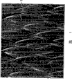
Fig. 3 is the amplification plan view that comprises 90 degree drift angle macrostructures of nano-scale tubercle, and the tubercle of described nano-scale is used for widening 1/2 jiao of brightness (comparing with the macrostructure with smooth side wall).The nano-nodules of the projection among Fig. 3 is distributed on 95% the surface of macrostructure haply, and little nano-nodules is overlapping and intersect.In Fig. 3, nano-nodules and macrostructure are whole, are made by identical materials.Because described nano-nodules is whole, they have splendid adhesiveness, have reduced the possibility that nano-nodules separates with described macrostructure.In addition, because described nano-nodules and described macrostructure are whole, the luminous energy of transmission couples light in the nano-nodules, has eliminated the undesirable scattering or the reflection that may reduce blooming efficient.Nano-nodules among Fig. 3 is the tubercle of projection, and its shape often is roughly ellipse.The Ra of the nano-nodules 300 among Fig. 3 is 925 nanometers, and the mean diameter that the nano-nodules among Fig. 3 records is 1.08 microns.Nano-nodules among Fig. 3 is approximate to be distributed on the surface of described macrostructure with normal distribution, and standard deviation is 38 nanometers.
In an embodiment of the invention, described nano-nodules preferably covers and surpasses 95% macrostructure surface area.The amount that has been found that surface area coverage is the photodistributed important determinative of the outgoing of blooming.By the coverage rate greater than 95% is provided, can the visual angle be optimized at specific nano-nodules size, shape and macrostructure geometric configuration.In yet another embodiment of the present invention, described nano-nodules preferably covers the macrostructure surface of 65-85%.Cover the macrostructure that surpasses 95% surface area with the macrostructure that does not have any nano-nodules or nano-nodules and compare, by the coverage rate of 65-85% is provided, described blooming can have simultaneously and redirects and high visual angle characteristic.
In yet another embodiment of the present invention, comprise nano-nodules with described light-emitting face opposite surfaces.Provide other light diffusion with the nano-nodules on the light-emitting face opposite surfaces, can significantly not reduce the ability that described macrostructure makes the recycle of low-angle incident light simultaneously.Nano-nodules on the face opposite with light-emitting face can also reduce the visible defects in the blooming, when blooming of the present invention contacts with other surface, provide light away from.At last, the existence of the nano-nodules on the face opposite with light-emitting face provides splendid blooming to transport the surface, reduces cut and wearing and tearing in the manufacture process.
Described blooming preferably comprises the film that has protruding macrostructure on light-emitting face, the length of described macrostructure, diameter or other key dimension are at least 25 microns, and the Ra value on the surface of described macrostructure is not more than 1200 nanometers.Mean roughness, or Ra, the peak between the expression nano-nodules is measured by profilograph to the average height of paddy, and the result represents with nanometer.By R is provided
aMacrostructure less than 1200, described blooming provide high brightness and wide visual angle simultaneously.Mean diameter has reduced the amount of collimation greater than the macrostructure of 1500 nanometers, causes the overall brightness of film that the minimizing that occurs takes place not wish.
In yet another embodiment of the present invention, the Ra value of described surperficial macrostructure is the 600-1000 nanometer.Have been found that the average rugosity in surface can provide collimation and the wide visual angle that is applicable to the LCD TV applications simultaneously for the macrostructure of 600-1000 nanometer.
The size of described macrostructure, shape and distribution are very important for decision from the distribution of the light of macrostructure outgoing.Preferred depth-width ratio is the macrostructure of 0.5-6.0.Depth-width ratio is very little for increasing an influence of going up gain less than 0.2 macrostructure.Depth-width ratio is difficult to use molten polymer to cast on the figuratum metallic roll greater than 6.0 nano-nodules to form, because described polymkeric substance tends to stick on the surface with high depth-width ratio feature.In addition, need high pressure to be completed into the feature of described high depth-width ratio, this has significantly reduced the life-span of mould.
In an embodiment of the invention, described macrostructure has repeat patterns.Because compare with macrostructure at random, repeat patterns has higher bulk density, so repeat patterns provides a spot of undesirable patternless zone usually.In yet another embodiment of the present invention, described macrostructure preferably has random pattern.Although because compare with repeat patterns, random pattern has lower bulk density, described random pattern can form some patternless bloomings really usually, compares with repeat patterns, and random pattern can produce the moir than low degree usually really.Shown that also random pattern can hide or cover little film defective, in order to avoid its observed person's eyes are seen.
In yet another embodiment of the present invention, the length of described macrostructure, diameter or other size are at least 100 microns.Size provides the axle that need provide greater than 1.0 to go up the required collimation of incident light that gains greater than 100 microns micromechanism.In addition, do not have the more difficult manufacturing of micromechanism, because such size may cause undesirable patternless zone on blooming greater than 100 microns size.
The optical alignment macrostructure can hinder the incident light transmission that is in off-axis angle usually, allows to be in the transmittance on the last or approaching axle of axle.Usually, the collimation macrostructure angle-brightness curve be presented at 0 the degree or its near high-high brightness is arranged, then near 90 the degree angles reducing of brightness appearring.The slope that brightness reduces is the function of macrostructure geometric configuration.Have been found that significant change can take place in the variation of slope by certain roughness is provided on the surface of macrostructure, so that the brightness of increase is provided in wideer angular range.In the preferred embodiment of the present invention, preferably blooming is included in the film that has raised or sunken macrostructure on the light-emitting face, and the length of described macrostructure, diameter or other size are at least 25 microns, the R on the surface of described macrostructure
aBe worth enough lowly, can make a last gain of light be reduced by at least 25% (arrange with the identical macrostructure that does not have described surfaceness and compare).Have been found that axle goes up gain and reduce at least 25% and can cause the brightness on the desirable off-axis angle to increase (comparing with level and smooth macrostructure), the result obtains having the blooming of improved lightness properties.
Fig. 2 is a rough schematic view of making the equipment of blooming, for example can be used to make blooming shown in Figure 3.Described equipment comprises extruder 201, these extruder 201 extruded materials 203.Described equipment also comprises figuratum roller 205, and described roller 205 comprises the macrostructure with nano-nodules, is used for forming optical signature in optical layers 213.In addition, described equipment comprises pressure roll 207, is used to provide pressure, and material 203 is pressed in the figuratum roller 205, also comprises stripper roll 211, material 203 is taken off from figuratum roller 205 with helping.
In operation, between pressure roll 207 and figuratum roller 205, basalis 209 is exerted pressure with the material of extruding 203.In an exemplary embodiment, described basalis 209 is polymer sheets of orientation.In addition, described material 203 has formed optical layers 213, and described optical layers 213 comprises optical signature after between by described figuratum roller 205 and pressure roll 207.Perhaps, can be at extruder 201 with bonding coat and 203 coextrusion of described material.Coextrusion provides the benefit of two or more layers.Can be selected to basalis 209 and optical layers 213 to the bonding coat of coextrusion best cohesive is provided, produce the cohesive higher than individual layer.Therefore, the bonding coat of described coextrusion and optical layers are under pressure with basalis between described pressure roll 207 and figuratum roller 205.After having passed through between described pressure roll 207 and the figuratum roller 205, make layer 213 by roller 211.In embodiment, layer 213 is optical textures of the embodiment described in detail among following Fig. 3.
Another preferred embodiment in, described material 203 comprises the coextrusion layer of polymkeric substance, it comprises cortex, described cortex contacts with the roller 205 that the nano-nodules pattern is arranged, the melt index (MI) of cortex is than remaining floor height 50% in the structure of described coextrusion.The cortex that has been found that high fluidity helps the accuracy of duplicating of polymkeric substance.Layer beyond the cortex has much lower melt index (MI), and harder blooming on the mechanical property that obtains can be suitable for tolerating the strict demand of display device better.
Described have the roller of nano-nodules pattern to preferably include metallic roll, and it comprises the substrate macrostructure that is covered by nano-nodules.Described macrostructure can machining form or be arranged at random on the surface of described roller.Known technology, for example diamond turning, spray pearl, impression, miniature carving pressure or electricapparatus engraving have been shown to form the acceptable macrostructure.Preferably,, nano-nodules is put on equably on the surperficial macrostructure of machining in the metallic roll, to guarantee the having connection that effectively continues between described base metal and the surface by in fluoride bath, carrying out accurate electrochemical deposition.Electrolytic process applies thin and fine and close chromium layer, obtains than (being electroless nickel plating etc.) coating that applies under the situation that does not make electricity consumption or the better combination of coating.Assemble 0.25 the minimal deposition thickness of micron can prevent hydrogen, this situation perplexs electroless plating through regular meeting.Thin and fine and close nodositas chromium is hard chromium, and it is extremely thin, and the Shang Buhui accumulation is enough to cause the stress of crackle, therefore has good anti-corrosion.The high chromium nonmagnetic alloy of deposition compact equably on the surface of described metal macrostructure.In addition, the metal macrostructure that has shown the nodositas chromium fine and close with not adding described approaching is compared, described thin and fine and close nodositas chromium can improve lubricity, prevent wearing and tearing, improve mar proof, have lower friction factor, splendid anti-sticking to mould (antisei zure) characteristic is provided, have lower corrosion resistance.
The thickness that the thin and fine and close chrome plating of this macrostructure applies can be the 0.25-4.0 micron.Have been found that the described thin and fine and close chromium layer that macrostructure is applied is thicker, can increase the diameter of described nano junction node, reduce the axle of described blooming and go up brightness.Described thin and fine and close chromium deposition preferably carries out under low temperature, is usually less than 60 ℃, can be used for all ferrous metals and non-ferrous metal, can not cause distortion simultaneously.By fixed part and control plating bath carefully, can accurately control thickness deviation.In addition, tubercular thin and fine and close chrome plating can be at the angle or sharp-pointed edge demonstrate undesirable accumulation.Have been found that the profile of described nano-nodules, have accurate deposit thickness, therefore can make macrostructure form tubercle very uniformly according to the macrostructure of described base metal.
In one of the present invention preferred embodiment, described thin and fine and close nano-nodules is applied on the surface of described macrostructure with the form of pattern.The pattern form deposition of described nano-nodules can be finished in the following manner: a plurality of parts or each macrostructure of pair roller are sheltered, and make do not have nano-nodules on a part of surface of described roller or on the desired zone of each macrostructure.The nano-nodules that pattern form applies also preferably can be according to certain gradient, is applied to corresponding on the macrostructure of the edge of LCD display or central area or on the bigger area.
Under the situation that the technology with thin and fine and close nodositas chromium applies, the hardness number of coating is the 70-80 HRC.By the hardness of 70-80 HRC is provided, can form described macrostructure with base metal (comprise hardened steel, for example record 62 Rockwell's hardnesss) softer, easier machining.In addition, the natural lubricity of chromium, and have and be used for the outstanding coating that reduces wear and rub, can prevent wearing and tearing and sticking to mould, can improve release property at the polymkeric substance of figuratum roller top casting.
Described nano-nodules also can put on the surface of described macrostructure by methods known in the art (for example spraying pearl, sandblast, little grinding or micro-indentations).
Of the present invention another preferred embodiment in, preferably optical device comprises the film that has raised or sunken macrostructure on the light-emitting face, the length of described macrostructure, diameter or other key dimension are at least 25 microns, and the major part on described macrostructure surface is covered by the nano-nodules of mean diameter less than 1200 nanometers.Thereby described device preferably includes and uses light control film change incident direction of light to improve the quality of display or the display device of character.Preferred devices includes but not limited to LCD, OLED, the projection display, plasma display and PLED.
The present invention can be used in combination with liquid crystal display device arbitrarily, and the conventional structure of this device is as mentioned below.Liquid crystal (LC) is widely used in electronic console.In these display systems, the LC layer is located between polarizer layer and the analyzer layer, has guides, and this guides shows the position angle distortion by described layer with respect to normal axis.The orientation of described analyzer make its absorption axes perpendicular to polarizer the axle.The incident light that is polarized the device polarization is subjected to the molecular orientation influence in the liquid crystal by liquid crystal cell, and the molecular orientation of described liquid crystal can change by the voltage that is applied on the described liquid crystal cell.By using this kind principle, can control transmission from the light (comprising surround lighting) of external light source.Reach the required energy of this control usually much smaller than the middle required energy of luminescent material that uses of other Display Types (for example cathode-ray tube (CRT)).Therefore, people are used for many application with the LC technology, include but not limited to digital watch, counter, and portable computer, electronic game machine is used for these, and is in light weight, energy consumption is low and long service life is very important feature.
Active matrix liquid crystal display (LCD) uses thin film transistor (TFT) (TFT) as switching device, is used to drive each liquid crystal pixel.
These LCD can demonstrate the more image of high definition, can not cause simultaneously and crosstalk, because each liquid crystal pixel can be selectively driven.It is the LCD of a kind of " white usually " that optical mode disturbs (OMI) display, that is to say, light is to close the closed state transmission by the display layer.Use the operator scheme of the LCD of twisted nematic liquid crystal to be broadly divided into birefringent mode and light rotary mode." supertwist of film compensation is to row " are LCD black normally (FSTN), that is to say that when not applying voltage, under the situation of closing closed state, transmittance is suppressed.It is reported that the OMI display has response time and wideer operating temperature range faster.
The ordinary ray that the incandescent lamp or the sun produce is a random polarization, that is to say, it is included in the light wave of all possible direction orientation.Polarizer is that its effect is to remove a kind of from two kinds of the incident beam vertical plane polarization components by selectivity, the light beam of (" the not polarization ") of random polarization is converted into the dichroic material of light beam.Linear polarization is the critical component of LCD (LCD) device.
There is the polarizer of the high dichroic ratio of several classes can handle the optical property that is enough to be used in the LCD device.These polarizers are made by some thin slices of material, and the component that these materials can a kind of polarization of transmission absorbs other mutually orthogonal component (this effect is called as dichromatism) simultaneously.The most frequently used plastic sheet polarizer is made up of polyvinyl alcohol (PVA) (PVA) film of uniaxial tension, and wherein the PVA polymer chain is more or less aligned with parallel form.Described then aligned PVA with iodine molecule or coloured dichroic dye (for example referring to EP 0 182 632 A2, Sumitomo Chemical company limited) combination is mixed, these alloys can be adsorbed in PVA, and become the uniaxial orientation form by PVA, with make have in the high anisotropy matrix of grey.Then for the described fragility PVA film of mechanical support, stacked hard triacetyl cellulose (TAC) layer or similar supporting course in both sides.
Contrast, color rendition and stable gray-scale intensity are to use the important quality characteristic of the electronic console of liquid crystal technology.The principal element of contrast of restriction LCD is that light " leaked " and is in dark or the liquid crystal cell of " black " pixel status or the tendency of liquid crystal cell.In addition, the light leak of LCD (also being contrast) also depends on the viewing angle to indicator screen.Usually best contrast only can be observed in the very narrow on every side visual angle of display incident normal, and along with the visual angle increases, contrast can reduce rapidly.In color monitor, the light leak problem not only can reduce contrast, and can bring color or tonal variation because of the color rendition reduction.Except black attitude light leak, because the optical anisotropy of liquid crystal material, the problem of narrow viewing angle is by further worsening as the displacement of function of viewing angle in brightness-voltage curve in the conventional twisted nematic liquid crystal display.
When in back light system, as the light-diffusing films time, described film makes the brightness equalization with blooming of the present invention.The screen of backlight LCD display, the screen that for example is used for portable computer, the light source (for example fluorescent light) that may have relative localization, therefore the array of the light source of perhaps relative with the described lcd screen close relative localization that is provided with can detect each the " focus " corresponding with light source.Described diffuser is used for making the illumination equalization on the display.Described liquid crystal display device comprises the display device with following characteristic: it has and is selected from the driving method that for example driven with active matrix and simple matrix drive, and the combination that is selected from the liquid crystal mode of twisted nematic liquid crystal, super twisted nematic liquid crystal, ferroelectric liquid crystals and anti ferroelectric liquid crystal, but, the invention is not restricted to above combination.In liquid crystal display device, need alignment films of the present invention to be arranged on front backlight.Blooming of the present invention can make brightness even on liquid crystal display device, and this is because described film has splendid light scattering, can make that light scatters, and splendid observability is provided on all directions.Even, can be used in combination the film of multilayer although use the such film of individual layer also can reach above-mentioned effect.In transmission mode, described homogenization film can be arranged on LCD material front, with minute luminous intensity distribution and make it more even.
Important use of the present invention is to eliminate (destrcturing) device as light source.In many application, wish from the output of light source itself, to eliminate the structure of filament, in some applications, the structure of this filament may throw into question, because the light that distributes in sample may change, is that people are undesirable therefore.In addition, after having replaced light source, the variation of filament of light source or arc orientation may produce error, causes the misleading result of reading.By homogenization film of the present invention is arranged between light source and the detecting device, can from the output of light source, eliminates the filamentray structure of any trace, thereby obtain the output of identical homogenization by different light sources.
The light of the homogenization of the pleasant by required direction is provided can be controlled stage illumination, lighting with described blooming.In producing with televisor before the lights, must use many kinds of lights of stage to obtain all required different effects of suitable illumination.This need use many different lamps, and this is very inconvenient and expensive.The film of the present invention that is arranged on the lamp almost can provide unrestricted dirigibility that light is disperseed.Therefore, can correctly shine almost any object, whether no matter move, which kind of shape all can.
Can be applied to by reflection horizon on the light-emitting face of blooming of the present invention, form the reflection horizon formations such as metal films, can be as for example retroeflection parts of traffic lights.Can be applied to automobile, bicycle, individual with a kind of state waits and uses.
Blooming of the present invention also can be used for law enforcement and field of security systems, makes that in whole safety zone the output homogenization of laser diode (LD) or light emitting diode (LED) is to provide with respect to the higher contrast of infrared (IR) detecting device.Film of the present invention also can be used to remove structure from the device that uses LED or LD source, for example is used for bank's cash inspecting machine or skin treating device.This produces higher accuracy rate.
If in surgical procedure, a fiber optic component fracture is installed in the optical fiber optical assembly on the surgical cap, may cause the light that throws on field of operation to disperse Strength Changes.Blooming of the present invention is placed the end of fibre bundle, make light homogenization, and eliminated the optical fiber of the fracture of any trace the light on being incident upon the patient from remaining optical fiber.The ground glass diffusing globe of standard can not be used for this kind purposes effectively, passes through light loss because significant backscattering can cause.
Blooming of the present invention can also be by the filament or the arc of elimination light source, the visual field of evenly being thrown light on, thus the sample under adjusting the telescope to one's eyes throws light on uniformly.Film of the present invention can also be used to the various patterns by Optical Fiber Transmission are carried out homogenization, for example can be to light output the carrying out homogenization by helicon mode optical fiber.
Blooming of the present invention also has important building occupancy, for example for work and the living space suitable illumination is provided.In the commerce of routine is used, use cheap transparent polymer diffuser to help diffused light to be dispersed in the room.A kind of homogenizer of the present invention has replaced one of these conventional diffusing globes, and the output of more uniform light is provided, so light disperses with all even angle ground in the room, does not have focus.
Blooming of the present invention also can be used to light diffusion is thrown light on to the artwork.Described transparent polymeric membrane diffusing globe provides the hole of suitable dimension and orientation, is used in the most desirable mode the artwork being thrown light on.
In addition, blooming of the present invention can be widely used as the part of optical device (for example display device).For example, except the light diffuser plate of the back light system of above-mentioned liquid crystal display device, in reflective type liquid crystal display device, it can be used as and reflectance coating such as the stacked light reflecting board of metal film, perhaps under the situation of the back side that metal film is arranged on device (face opposite) with the observer, as preceding scattering film, with film towards the front (beholder one side).Can blooming of the present invention be used as electrode by the stacked transparency conducting layer of forming by indium oxide (being expressed as the ITO film).If described material is used for forming reflective viewing screen, for example front projection screen then is applied to reflection layer on the described transparent polymkeric substance diffusing globe.
It is the back projection screen that the another kind of described blooming is used, this usually need with light source with image projection on very large-area screen.TV visual angle in vertical direction is usually less than in the horizontal direction visual angle.The effect of described blooming is that light is scattered, to increase the visual angle.
Embodiments of the present invention can provide and not only improve light diffusion and collimation, and can also reduce the blooming of thickness, this film has the tendency of the light absorption of minimizing, and the angle that shows mitigation is ended, and perhaps shows moir or the Newton ring that reduces in the LCD display system.
Although specifically describe the present invention in detail, be to be understood that and carry out changes and improvements within the spirit and scope of the present invention with reference to some of the preferred embodiment of the invention.
Embodiment
In the present embodiment, nano-nodules is applied to the light with 90 degree drift angles redirects on the surface of macrostructure, have the blooming that wide angle light distributes, makes the light scattering minimum simultaneously with formation.To have the light output that redirects macrostructure that is applied to described lip-deep nano-nodules compares with the LCD level light diffuser and the LCD level light-redirecting film of prior art.
The metallic roll electricapparatus that is coated with high temperature nickel is carved out each macrostructure with 90 degree drift angles.The depth capacity of described each element is 35 microns, and width is 40 microns, and length is 1200 microns.To the thin and fine and close chromium of metallic roll plating of the nickel plating of described electricapparatus engraving, on the surface of the macrostructure of electricapparatus engraving, form nano-nodules.Fig. 5 is the vertical view that has each optical element of nano-nodules on the surface of each element.The Ra of the nano-nodules among Fig. 5 is 823 nanometers, and the mean diameter that the nano-nodules among Fig. 5 records is 942 nanometers.Described nano-nodules lognormal distribution from the teeth outwards, the intermediate value of nano-nodules is 802 nanometers.As expection, the nano-nodules density in the paddy zone of Fig. 5 is greater than the more smooth zone of macrostructure, because nano-nodules tends to towards the growth of sharp peak.Be to be understood that by reducing the sharp peak of described macrostructure, can reach the purpose that nano-nodules is set more equably on the surface of macrostructure.
Fig. 4 is the contrast of blooming (400 and 404) with the pitch angle-brightness curve of the blooming 402 of embodiment of two kinds of prior aries.On ELDIM, carry out the measurement of brightness.50 cm diagonal line LCD TV airborne measurements comparative film and the feature films that comprise the back-lighting backlight of 12 CCFL bulbs in use.LCD level body diffusing globe is placed on the described CCFL bulb, is used for described ELDIM and measures.Curve 406 is the output valves that are used for the body diffusing globe of this measurement.The normal brightness that the axle that curve 400 expression is used for improving conventional LCD display is gone up brightness improves the numerical value that film records.Go up brightness although curve 400 has high axle really, from axle (tilt angle of zero) rate of curve height, this may cause at the off-axis angle place, and the luminance loss of LCD display part reduces from the axle color saturation.Curve 404 expression is used for numerical value that the standard TV diffusing globe that carries out diffusion from televisor light backlight is recorded.Although diffusing globe 404 can pass through the scatter incident light energy and diffusion backlight really, diffusing globe 404 does not have sufficiently high axle and goes up brightness, and this is because conventional LCD light diffuser can carry out scattering to transmitted light.
The numerical value that the curve 402 expressions macrostructure that is covered by nano-nodules shown in Figure 5 records.Compare with brightness film 400, described wide angle alignment film 402 has high axle simultaneously and goes up gain and little of the axle slope, allow materials control of the present invention to penetrate light source and carry out diffusion, provide high axle to go up luminance gain, constant relatively illumination is provided in wideer tilt angle ranges simultaneously.The feature of the collimated light beam of curve 402 expression incident lights makes within required angular width scattered intensity-pitch angle curve substantially flat.
List of parts
2 macrostructures
201 extruders
203 materials of extruding
205 figuratum rollers
207 pressure rolls
209 basalises
211 stripper roll
213 optical layers
300 nano-nodules
The curve of 400 prior art films
402 films of the present invention
The film of 404 prior aries
406 not improved light outputs
500 nano-nodules
Claims (17)
1. a light redirects optical device, it comprises the polymeric membrane with light entrance face and light-emitting face, on described light-emitting face, has protruding macrostructure, the length of this projection macrostructure, diameter or other key dimension are at least 25 microns, the major part on described macrostructure surface is covered by nano-nodules, described nano-nodules perpendicular to the average maximum thick line length in the plane of optical transmission direction less than 1200 nanometers.
2. device as claimed in claim 1 is characterized in that, the average diameter size of described nano-nodules is the 400-1200 nanometer.
3. device as claimed in claim 1 is characterized in that, the average diameter size of described nano-nodules is the 600-1000 nanometer.
4. device as claimed in claim 1 is characterized in that described nano-nodules caves in.
5. device as claimed in claim 1 is characterized in that described nano-nodules is protruding.
6. device as claimed in claim 1 is characterized in that described macrostructure comprises prism.
7. device as claimed in claim 1 is characterized in that described nano-nodules comprises polymkeric substance.
8. device as claimed in claim 1 is characterized in that, described nano-nodules and described macrostructure are integrations.
9. device as claimed in claim 1 is characterized in that described macrostructure comprises independent optical element.
10. device as claimed in claim 1 is characterized in that, the depth-width ratio of described macrostructure is 0.5-5.0.
11. device as claimed in claim 1 is characterized in that, the gain of light of described blooming is 1.15-1.30.
12. device as claimed in claim 1 is characterized in that, described nano-nodules and described macrostructure are integrations, have covered the surface area of the described macrostructure of 40-60%.
13. device as claimed in claim 1 is characterized in that, described nano-nodules is randomly dispersed on the surface of described macrostructure, the diameter overlapping at least 5% of described nano-nodules.
14. device as claimed in claim 1 is characterized in that, described nano-nodules has covered and has surpassed 95% described macrostructure surface.
15. device as claimed in claim 1 is characterized in that, described nano-nodules has covered the described macrostructure surface of 65-85%.
16. blooming, it is included in the film that has raised or sunken macrostructure on the light-emitting face, the length of described macrostructure, diameter or other key dimension are at least 25 microns, compare with the identical macrostructure layout that does not have described surfaceness, the Ra value on the surface of described macrostructure is low to be reduced by at least 25% to being enough to make axle go up the gain of light.
17. method of making metal form, described metal form comprises the surface with macrostructure geometric configuration, said method comprising the steps of: on the surface of metal form, carry out the electricapparatus engraving, plating is carried out on surface to described metal form, forms metal nano tubercle coating on the surface of described macrostructure.
Applications Claiming Priority (2)
| Application Number | Priority Date | Filing Date | Title |
|---|---|---|---|
| US11/393,024 | 2006-03-30 | ||
| US11/393,024 US20080081132A1 (en) | 2006-03-30 | 2006-03-30 | Light redirecting film having surface nano-nodules |
Publications (1)
| Publication Number | Publication Date |
|---|---|
| CN101438191A true CN101438191A (en) | 2009-05-20 |
Family
ID=38330482
Family Applications (1)
| Application Number | Title | Priority Date | Filing Date |
|---|---|---|---|
| CNA2007800159321A Pending CN101438191A (en) | 2006-03-30 | 2007-03-16 | Light redirecting film having surface nano-nodules |
Country Status (7)
| Country | Link |
|---|---|
| US (1) | US20080081132A1 (en) |
| EP (1) | EP2002293A1 (en) |
| JP (1) | JP2009532714A (en) |
| KR (1) | KR20080108260A (en) |
| CN (1) | CN101438191A (en) |
| TW (1) | TW200741310A (en) |
| WO (1) | WO2007126607A1 (en) |
Cited By (3)
| Publication number | Priority date | Publication date | Assignee | Title |
|---|---|---|---|---|
| CN102656488A (en) * | 2009-12-17 | 2012-09-05 | 3M创新有限公司 | Light redirecting constructions |
| CN102656489A (en) * | 2009-12-17 | 2012-09-05 | 3M创新有限公司 | Light redirecting film laminate |
| CN113574441A (en) * | 2018-12-28 | 2021-10-29 | 脸谱科技有限责任公司 | Planarization of overcoat on sloped surface relief structures |
Families Citing this family (8)
| Publication number | Priority date | Publication date | Assignee | Title |
|---|---|---|---|---|
| US20100302479A1 (en) * | 1996-03-21 | 2010-12-02 | Aronson Joseph T | Optical article |
| US20080024870A1 (en) * | 2006-07-27 | 2008-01-31 | Bourdelais Robert P | Light-redirecting film containing optical modification layer |
| US7530726B2 (en) * | 2007-03-06 | 2009-05-12 | Skc Haas Display Films Co., Ltd. | Light redirecting film having discontinuous coating |
| KR20100091215A (en) * | 2007-11-19 | 2010-08-18 | 쓰리엠 이노베이티브 프로퍼티즈 컴파니 | Articles and methods of making articles having a concavity or convexity |
| US8675061B2 (en) * | 2010-11-01 | 2014-03-18 | Richard D. Balentine | Digital video projection display system |
| US10183318B2 (en) * | 2011-09-23 | 2019-01-22 | Boegli-Gravures S.A. | Method and device for producing a structured surface on a steel embossing roller |
| EP3122533A4 (en) | 2014-03-24 | 2018-03-21 | Inmold A/S | Method and apparatus for producing a high aspect ratio nanostructured foil by extrusion coating or extrusion casting |
| EP3230041A1 (en) | 2014-12-10 | 2017-10-18 | Inmold A/S | Method and apparatus for producing a nanostructured or microstructured foil by extrusion coating or extrusion casting |
Family Cites Families (19)
| Publication number | Priority date | Publication date | Assignee | Title |
|---|---|---|---|---|
| JPH09159810A (en) * | 1995-10-05 | 1997-06-20 | Sekisui Chem Co Ltd | Optical control sheet and surface light emitting device having the same |
| US5919551A (en) * | 1996-04-12 | 1999-07-06 | 3M Innovative Properties Company | Variable pitch structured optical film |
| US5829240A (en) * | 1997-03-17 | 1998-11-03 | A. B. Carter, Inc. | Spinning ring having improved traveler bearing surface |
| CA2318790C (en) * | 1998-02-18 | 2004-03-30 | Minnesota Mining And Manufacturing Company | Optical film |
| US6752505B2 (en) * | 1999-02-23 | 2004-06-22 | Solid State Opto Limited | Light redirecting films and film systems |
| AU2001279319A1 (en) * | 2000-08-01 | 2002-02-13 | James Cowan | Directional diffuser |
| JP4225675B2 (en) * | 2000-09-07 | 2009-02-18 | 富士フイルム株式会社 | Antiglare antireflection film and liquid crystal display device |
| KR100432438B1 (en) * | 2001-01-18 | 2004-05-22 | 주식회사 송산 | Prism Diffuser |
| US20030035231A1 (en) * | 2001-08-03 | 2003-02-20 | Epstein Kenneth A. | Optical film having microreplicated structures; and methods |
| US6583936B1 (en) * | 2002-03-11 | 2003-06-24 | Eastman Kodak Company | Patterned roller for the micro-replication of complex lenses |
| US6721102B2 (en) * | 2002-03-11 | 2004-04-13 | Eastman Kodak Company | Surface formed complex polymer lenses for visible light diffusion |
| JP4506070B2 (en) * | 2002-11-01 | 2010-07-21 | コニカミノルタホールディングス株式会社 | Method for forming antiglare layer, method for producing antiglare film, and ink jet device for forming antiglare layer |
| US7046439B2 (en) * | 2003-05-22 | 2006-05-16 | Eastman Kodak Company | Optical element with nanoparticles |
| US7074463B2 (en) * | 2003-09-12 | 2006-07-11 | 3M Innovative Properties Company | Durable optical element |
| TWI328702B (en) * | 2003-11-04 | 2010-08-11 | Hon Hai Prec Ind Co Ltd | Backlight system |
| US7106517B2 (en) * | 2003-12-31 | 2006-09-12 | General Electric Company | Display optical films |
| TW200600919A (en) * | 2004-06-22 | 2006-01-01 | Samsung Electronics Co Ltd | Optical film, backlight assembly and liquid crystal display device having the same |
| US7277609B2 (en) * | 2004-11-05 | 2007-10-02 | Optical Research Associates | Methods for manipulating light extraction from a light guide |
| US20080024870A1 (en) * | 2006-07-27 | 2008-01-31 | Bourdelais Robert P | Light-redirecting film containing optical modification layer |
-
2006
- 2006-03-30 US US11/393,024 patent/US20080081132A1/en not_active Abandoned
-
2007
- 2007-03-16 KR KR1020087023928A patent/KR20080108260A/en not_active Application Discontinuation
- 2007-03-16 EP EP07753343A patent/EP2002293A1/en not_active Withdrawn
- 2007-03-16 JP JP2009502842A patent/JP2009532714A/en active Pending
- 2007-03-16 WO PCT/US2007/006708 patent/WO2007126607A1/en active Application Filing
- 2007-03-16 CN CNA2007800159321A patent/CN101438191A/en active Pending
- 2007-03-29 TW TW096111057A patent/TW200741310A/en unknown
Cited By (5)
| Publication number | Priority date | Publication date | Assignee | Title |
|---|---|---|---|---|
| CN102656488A (en) * | 2009-12-17 | 2012-09-05 | 3M创新有限公司 | Light redirecting constructions |
| CN102656489A (en) * | 2009-12-17 | 2012-09-05 | 3M创新有限公司 | Light redirecting film laminate |
| CN102656489B (en) * | 2009-12-17 | 2015-09-02 | 3M创新有限公司 | Light-redirecting film lamilated body |
| CN106199793A (en) * | 2009-12-17 | 2016-12-07 | 3M创新有限公司 | Light redirects structure |
| CN113574441A (en) * | 2018-12-28 | 2021-10-29 | 脸谱科技有限责任公司 | Planarization of overcoat on sloped surface relief structures |
Also Published As
| Publication number | Publication date |
|---|---|
| US20080081132A1 (en) | 2008-04-03 |
| WO2007126607A1 (en) | 2007-11-08 |
| JP2009532714A (en) | 2009-09-10 |
| KR20080108260A (en) | 2008-12-12 |
| TW200741310A (en) | 2007-11-01 |
| EP2002293A1 (en) | 2008-12-17 |
Similar Documents
| Publication | Publication Date | Title |
|---|---|---|
| CN101438191A (en) | Light redirecting film having surface nano-nodules | |
| US7543974B2 (en) | Light redirecting film having variable thickness | |
| KR101172411B1 (en) | Surface formed complex polymer lenses for visible light diffusion | |
| US6583936B1 (en) | Patterned roller for the micro-replication of complex lenses | |
| CN101310198B (en) | Multi-function enhancement film | |
| US7367705B2 (en) | Long curved wedges in an optical film | |
| JP5823958B2 (en) | Light re-deflecting film and display using the film | |
| CN101221255B (en) | Light-redirecting film containing optical modification layer | |
| TWI449942B (en) | Light redirecting film having discontinuous coating | |
| CN101341429A (en) | Low birefringent light redirecting film | |
| US7738754B2 (en) | Optical component and backlight unit using the optical component | |
| TWI781837B (en) | Display | |
| US7236303B2 (en) | Thermoplastic optical feature with high apex sharpness | |
| JPH11306829A (en) | Light guide plate, surface light source device and reflecting type liquid crystal display device | |
| JPH09160024A (en) | Back light and liquid crystal display device using the back light | |
| KR100920371B1 (en) | Light-diffusing film for direct back light unit of lcd | |
| KR100971387B1 (en) | method for manufacturing of prism sheet | |
| KR20150007153A (en) | Light-diffusing film, manufacturing method thereof and backlight unit | |
| KR20080099404A (en) | Manufacturing method of light-diffusing film |
Legal Events
| Date | Code | Title | Description |
|---|---|---|---|
| C06 | Publication | ||
| PB01 | Publication | ||
| C10 | Entry into substantive examination | ||
| SE01 | Entry into force of request for substantive examination | ||
| C02 | Deemed withdrawal of patent application after publication (patent law 2001) | ||
| WD01 | Invention patent application deemed withdrawn after publication |
Open date: 20090520 |