CN101437166A - Image pickup apparatus, method of correcting captured image data, and program - Google Patents
Image pickup apparatus, method of correcting captured image data, and program Download PDFInfo
- Publication number
- CN101437166A CN101437166A CNA2008101727249A CN200810172724A CN101437166A CN 101437166 A CN101437166 A CN 101437166A CN A2008101727249 A CNA2008101727249 A CN A2008101727249A CN 200810172724 A CN200810172724 A CN 200810172724A CN 101437166 A CN101437166 A CN 101437166A
- Authority
- CN
- China
- Prior art keywords
- pixel
- corrected parameter
- pixels
- group
- image pickup
- Prior art date
- Legal status (The legal status is an assumption and is not a legal conclusion. Google has not performed a legal analysis and makes no representation as to the accuracy of the status listed.)
- Pending
Links
Images


Classifications
-
- H—ELECTRICITY
- H04—ELECTRIC COMMUNICATION TECHNIQUE
- H04N—PICTORIAL COMMUNICATION, e.g. TELEVISION
- H04N23/00—Cameras or camera modules comprising electronic image sensors; Control thereof
- H04N23/10—Cameras or camera modules comprising electronic image sensors; Control thereof for generating image signals from different wavelengths
- H04N23/12—Cameras or camera modules comprising electronic image sensors; Control thereof for generating image signals from different wavelengths with one sensor only
-
- H—ELECTRICITY
- H04—ELECTRIC COMMUNICATION TECHNIQUE
- H04N—PICTORIAL COMMUNICATION, e.g. TELEVISION
- H04N23/00—Cameras or camera modules comprising electronic image sensors; Control thereof
- H04N23/80—Camera processing pipelines; Components thereof
- H04N23/84—Camera processing pipelines; Components thereof for processing colour signals
-
- H—ELECTRICITY
- H04—ELECTRIC COMMUNICATION TECHNIQUE
- H04N—PICTORIAL COMMUNICATION, e.g. TELEVISION
- H04N25/00—Circuitry of solid-state image sensors [SSIS]; Control thereof
- H04N25/10—Circuitry of solid-state image sensors [SSIS]; Control thereof for transforming different wavelengths into image signals
- H04N25/11—Arrangement of colour filter arrays [CFA]; Filter mosaics
- H04N25/13—Arrangement of colour filter arrays [CFA]; Filter mosaics characterised by the spectral characteristics of the filter elements
- H04N25/134—Arrangement of colour filter arrays [CFA]; Filter mosaics characterised by the spectral characteristics of the filter elements based on three different wavelength filter elements
-
- H—ELECTRICITY
- H04—ELECTRIC COMMUNICATION TECHNIQUE
- H04N—PICTORIAL COMMUNICATION, e.g. TELEVISION
- H04N25/00—Circuitry of solid-state image sensors [SSIS]; Control thereof
- H04N25/60—Noise processing, e.g. detecting, correcting, reducing or removing noise
- H04N25/62—Detection or reduction of noise due to excess charges produced by the exposure, e.g. smear, blooming, ghost image, crosstalk or leakage between pixels
-
- H—ELECTRICITY
- H04—ELECTRIC COMMUNICATION TECHNIQUE
- H04N—PICTORIAL COMMUNICATION, e.g. TELEVISION
- H04N25/00—Circuitry of solid-state image sensors [SSIS]; Control thereof
- H04N25/70—SSIS architectures; Circuits associated therewith
-
- H—ELECTRICITY
- H04—ELECTRIC COMMUNICATION TECHNIQUE
- H04N—PICTORIAL COMMUNICATION, e.g. TELEVISION
- H04N25/00—Circuitry of solid-state image sensors [SSIS]; Control thereof
- H04N25/70—SSIS architectures; Circuits associated therewith
- H04N25/76—Addressed sensors, e.g. MOS or CMOS sensors
- H04N25/77—Pixel circuitry, e.g. memories, A/D converters, pixel amplifiers, shared circuits or shared components
- H04N25/778—Pixel circuitry, e.g. memories, A/D converters, pixel amplifiers, shared circuits or shared components comprising amplifiers shared between a plurality of pixels, i.e. at least one part of the amplifier must be on the sensor array itself
-
- H—ELECTRICITY
- H04—ELECTRIC COMMUNICATION TECHNIQUE
- H04N—PICTORIAL COMMUNICATION, e.g. TELEVISION
- H04N9/00—Details of colour television systems
- H04N9/64—Circuits for processing colour signals
Abstract
An image pickup apparatus includes a solid-state image pickup device sharing a circuit necessary for a pixel structure between multiple pixels composing each set including a certain number of pixels having the same arrangement pattern; a pixel mixture correcting unit correcting leakage of light that should be incident on each pixel of the solid-state image pickup device from the pixel into adjacent pixels and/or leakage of light that should be incident on the adjacent pixels into the pixel in accordance with a correction parameter; a correction parameter generating unit generating multiple correction parameters corresponding to the multiple pixels composing the set; and a correction parameter selecting unit selecting the correction parameter from the multiple correction parameters in accordance with which pixel in the multiple pixels composing the set a pixel to be corrected corresponds to and supplying the selected correction parameter to the pixel mixture correcting unit.
Description
The cross reference of related application
The present invention comprises the relevant theme of submitting in Japan Patent office with on November 13rd, 2007 of Japanese patent application JP 2007-293875, and the combination here of its full content as a reference.
Technical field
The present invention relates to a kind of image pick-up device that is provided with solid-state image pickup (as complementary metal oxide semiconductors (CMOS) (CMOS)) imageing sensor, revise the method for the view data of catching and carry out the program of this method by this image pick-up device.
Background technology
Solid-state image pickup (as charge-coupled device (CCD) imageing sensor and cmos image sensor) is structure so, promptly is provided with the stacked lenticule that is useful on optically focused on the colour filter of the pixel cell that comprises optical-electrical converter below.
Pixel Dimensions reduces greatly along with the picture element density increase in recent years, can not ignore the problem of what is called " pixel mixing " in this image pickup device.Described pixel is mixed owing to following reason causes, and promptly pel spacing reduces, and is focused on the image pickup device and the light that passes colour filter not only incides on the pixel that wherein light will be assembled by lenticule, but also is easy to leak into adjacent pixels.
Figure 18 A and 18B illustrate described pixel mixing and how to take place.In the example shown in Figure 18 A and the 18B, image pickup device is a cmos image sensor 101, wherein is provided with below on the colour filter 103 of pixel cell 102 and is laminated with the convergent lens of being made up of lenticule 104.Above imageing sensor 101, be provided with aperture 105.
When aperture 105 is narrow inadequately in the example shown in Figure 18 A, the light that the opening by aperture 105 incides on the imageing sensor 101 not only incides on the object pixel unit 102, but also incides adjacent unit pixel 102.Therefore, the light that passes other colour filters 103 except that the colour filter 103 that is used for own pixel cell 102 incides each pixel cell 102.From the viewpoint of a pixel, should incide a part of light on described pixel pixel around from described pixel leaks to described pixel, and a part of light that should incide on the pixel around the described pixel but leaks in the described pixel.This phenomenon is called pixel and mixes.
On the contrary, when as in the example shown in Figure 18 B, aperture 105 is enough narrow and when inciding light in the imageing sensor 101 and only inciding on the pixel cell 102, described pixel does not take place mix.
Reduced separation property between the neighbor because described pixel is mixed, so reduced the resolution of output image.In addition, in the situation of monolithic image pick device (camera arrangement) with a solid-state image pickup, leak in the pixel because pass the light of the colour filter of different colours, so the color of image energy is thin out and/or can produce the geometrical pattern that depends on the blend of colors amount in the homogeneous area (the wherein content of image zone constant or that change a little) of image.Along with pel spacing narrows down, these problems generally can unexpected quality to output image produce adverse influence.
Not only ought be used for own pixel cell colour filter color be used for adjacent pixel unit colour filter color not simultaneously, but also when the color of the color of the colour filter that is used for adjacent pixel unit and the colour filter that is used for own pixel cell is identical, in this specification, pixel and the light of light around from a pixel leaks to described pixel leaks into described pixel from described neighbor and all is called pixel and mixes.
Therefore, remove wherein as in the monolithic colour image pick-up device, outside the situation of the colour filter of stacked different colours on the pixel cell, work as equally as all having in three color image pickup apparatus of a solid-state image pickup at colour filter for every kind of color, when the colour filter that is used for each image pickup device has same color, the light that incides on the image pick-up device not only incides on the pixel cell, but also the state that incides on the adjacent pixel unit is called the pixel mixing.
In the superincumbent situation, described pixel mixing can cause resolution to reduce, and the pixel that should have same color and brightness can change on the contrary.
To be used for revising the technology that described pixel mixes and to be included in the disclosed technology of Japanese unexamined publication application No.2007-142697 in order to address the above problem.In Japanese unexamined publication application No.2007-142697 in the basic handling of disclosed correction technique, add a following value for the value of object pixel, promptly the difference between the value of value by the object pixel that will revise will the solid-state image pickup from image pick-up device supplied with and neighbor multiply by the value that suitable correction factor (corrected parameter) obtains.In Japanese unexamined publication application No.2007-142697, described by to use the F number be described correction factor and control provider tropism (in direction between object pixel and the neighbor and the position poor).
In recent years, the solid-state image pickup that need use in video camera and digital camera more and more (as ccd image sensor and cmos image sensor) increases pixel count and reduces size.Size reduces and the pixel count increase can reduce the area of each pixel, thereby may reduce the pixel sensitivity degree.
In order to address this is that, by design circuit and distribution layout and/or improve manufacturing process and increase the ratio of photodiode in the dot structure of solid-state image pickup as much as possible, to obtain the increase of pixel count and reducing of size.Each dot structure is all by photodiode with comprise that the peripheral circuit of amplifier transistor and reset transistor forms.
Yet, requires solid-state image pickup increase pixel count recently more and more and reduce size, and the picture quality that improves when low light shines intensity has also caused attention.Therefore, the solid-state image pickup of the pixel sensitivity degree that can obtain to guarantee the ideal image quality only can not be provided by top behavior.
In this case, in order to overcome the above-mentioned defective of solid-state image pickup, the pixel technology of sharing has been subjected to extensive concern.In described pixel technology of sharing, between level each other and/or vertically adjacent or close a plurality of pixels, share the necessary a part of circuit of dot structure, for example amplifier transistor and/or reset transistor, area with the circuit (comprising distribution) that reduces each pixel, with the area of photodiode increase with the circuit of each pixel reduce the corresponding amount of area, improve the pixel sensitivity degree thus.
For example, Japanese patent application No.3838665 discloses a kind of pixel technology of sharing of sharing from necessary amplifier transistor of each pixel reads pixel data and reset transistor between two neighbors.In this technology, when with different slightly time Continuous Selection during with two neighbors that described amplifier transistor is connected with described reset transistor, from each pixel reads pixel data, thereby reduced the transistorized quantity of each pixel, the area increase of photodiode is reduced the corresponding amount of quantity with the transistorized of each pixel, thereby realized the raising of pixel sensitivity degree.
In not adopting the general solid-state image pickup of pixel technology of sharing, all usually pixel massiveness.In other words, all be general the pixel of any position of dot structure on screen of general solid-state image pickup.Therefore, in this general solid-state image pickup, the photodiode of all pixels all has identical peripheral environment in semiconductor structure.Thereby if get rid of the factor of any variation in the mill, then optical characteristics is identical basically for all pixels.
On the contrary, in adopting Japanese patent application No.3838665 for example in the typical solid-state image pickup of disclosed " pixel technology of sharing ", in the time will sharing described circuit and adjacent one another are or close a plurality of pixels and think a unit, all unit all have identical structure, and the pixel that is arranged in the diverse location place in each unit has different peripheral environments in semiconductor structure.Therefore, the Pareto diagram of sharing a plurality of pixels of described circuit carries out repetition, thereby produces circuit layout in the solid-state image pickup of taking described pixel technology of sharing.
Specifically, when a plurality of pixels that will share described circuit are thought a unit, in the solid-state image pickup of taking described pixel technology of sharing, repeat to arrange a plurality of unit horizontally and vertically.In semiconductor structure, has identical peripheral environment because be arranged in the photodiode of the pixel at same position place in the Pareto diagram in described a plurality of pixels in described a plurality of unit, so pixel has identical optical characteristics.
Yet the pixel (i.e. adjacent one another are or close pixel in each unit in described a plurality of unit) that is arranged in the diverse location place in described a plurality of unit in the Pareto diagram of described a plurality of pixels of sharing described circuit has different circuit and/or layout.Therefore, the photodiode of described pixel has different peripheral environments in semiconductor structure, thereby different pixel characteristic is provided.
Thereby, even catch the image of complete homogeneous target by the solid-state image pickup that adopts described " pixel technology of sharing ", still can be from the different pixel value of the neighbor each unit output, thereby, the problem that exists the quality of final output image to reduce greatly.
In the prior art, in order to solve the problems referred to above that pixel relates in sharing, for example at Japanese unexamined publication application No.2004-172950, Japanese unexamined publication application No.2005-110104 discloses many technology of the dot structure that is used to design solid-state image pickup among Japanese unexamined publication application No.2006-73733 and the Japanese unexamined publication application No.2006-157953.In these technology, for example (A) design pixel layout to reduce optical heterogeneity as much as possible or (B) so to carry out pixel and share, if optical heterogeneity promptly takes place, can influence output image sharply.
Summary of the invention
The disclosed technology that is used for revising " pixel mixings " is based on following supposition among the Japanese unexamined publication application No.2007-142697, all is identical (all pixels on the whole screen all have the pixel mixing of identical characteristics) characteristic all pixels on whole screen that promptly described pixel is mixed.
Therefore, passing through to use Japanese patent application No.3838665, Japanese unexamined publication application No.2004-172950, Japanese unexamined publication application No.2005-110104, disclosed any technology among Japanese unexamined publication application No.2006-73733 and the Japanese unexamined publication application No.2006-157953 and adopting in the solid-state image pickup of described pixel technology of sharing too must be eliminated the variation of sharing the pixel characteristic between the pixel.
Yet, as mentioned above, at Japanese unexamined publication application No.2004-172950, Japanese unexamined publication application No.2005-110104, the dot structure of design solid-state image pickup in the disclosed technology among Japanese unexamined publication application No.2006-73733 and the Japanese unexamined publication application No.2006-157953.Therefore, use design, can reduce to share the optical heterogeneity between a plurality of pixels (being called " sharing pixel " after sharing a plurality of pixels of circuit) of circuit, but can not eliminate its optical heterogeneity by the pixel of method (A) structure.
Thereby, because sharing the pixel characteristic of pixel changes, even so use the above-mentioned technology that is used for revising " pixel mixing ", in the solid-state image pickup apparatus of the pixel technology of sharing that adopts prior art, still can not revise described pixel mixing or some pixels fully and can be subjected to disadvantageous correction.As a result, there is the problem that the quality of output image is had adverse effect.
Also there is following problems,, in method A and B, can has strict restriction at the structure that reads of dot structure, layout or the pixel data of solid-state image pickup promptly in order to reduce to share the variation of the pixel characteristic between the pixel.In addition, can have strict restriction at the general image pick device of handling from the output of using method (A) or solid-state image pickup (B).
In order to solve top problem, in the solid-state image pickup that adopts described pixel technology of sharing, too, it is desirable to provide a kind of image pick-up device that can further reduce described pixel mixing to the influence of output image quality.
According to an embodiment of the invention, image pick-up device comprises solid-state image pickup, this solid-state image pickup is configured to share the necessary circuit of dot structure between a plurality of pixels of forming each group, described a plurality of pixel is arranged with two-dimensional array, the described group of pixel with aligned identical pattern that comprises specific quantity; Pixel is mixed correcting part, and it is used for should inciding on each pixel of described solid-state image pickup according to corrected parameter correction, and the light that leaks into the described pixel leaks but the light of the neighbor around from described pixel leaks to described pixel leaks and/or should incide on the described neighbor; The corrected parameter production part is used to produce a plurality of corrected parameters corresponding with described a plurality of pixels of forming described group; With the corrected parameter alternative pack, its according to the pixel that will mix the correcting part correction by described pixel corresponding to which pixel of forming in described a plurality of pixels of described group, select corrected parameter from described a plurality of corrected parameters that described corrected parameter production part is supplied with, and the corrected parameter of selecting is supplied to described pixel mixing correcting part.
Described corrected parameter production part produces and corresponding, promptly corresponding with the described shared pixel described a plurality of corrected parameters of described a plurality of pixels of forming described group.Described corrected parameter alternative pack basis will be corresponding with which shared pixel by the pixel of described pixel mixing correcting part correction, select the described corrected parameter corresponding from described a plurality of corrected parameters that described corrected parameter production part is supplied with, and the corrected parameter of selecting is supplied to described pixel mixing correcting part with the described pixel that will revise.
Therefore, equally in the solid-state image pickup of using the pixel technology of sharing, described pixel mixing correcting part mixes correction by using the described corrected parameter of setting to each shared pixel to carry out described pixel, thereby has further reduced the image of pixel mixing to output image quality.
According to the present invention, in the solid-state image pickup of using the pixel technology of sharing, need not design the dot structure of solid-state image pickup equally, can further reduce the image of pixel mixing to output image quality.
Description of drawings
Fig. 1 is the block diagram that shows the structure example of the image pick-up device of first execution mode according to the present invention;
Fig. 2 A illustrates the array of typical pixels of the solid-state image pickup that uses and the typical arrangement of colour filter to 2E in the described image pick-up device of first execution mode according to the present invention;
Fig. 3 is used for describing the diagrammatic sketch how described solid-state image pickup that uses from the described image pick-up device at first execution mode according to the present invention reads captive view data;
Fig. 4 A is the diagrammatic sketch that is used for being described in the Pareto diagram of shared pixel ID in the described solid-state image pickup that the described image pick-up device of first execution mode according to the present invention uses and shared pixel to 4C;
Fig. 5 is the block diagram that shows the structure example of the primary clustering in the described image pick-up device of first execution mode according to the present invention;
Fig. 6 A is the diagrammatic sketch that is used to describe the described image pick-up device of first execution mode according to the present invention to 6C;
Fig. 7 A is the diagrammatic sketch that is used to describe the described image pick-up device of first execution mode according to the present invention to 7D;
Fig. 8 is the block diagram that is presented at the structure example of the part in the structure example shown in Figure 5 in detail;
Fig. 9 A is the diagrammatic sketch that is used for describing from the processor output of structure example shown in Figure 8 to 9C;
Figure 10 illustrates the structure example of another processor in structure example shown in Figure 8;
Figure 11 is the block diagram that is presented at the structure example of another processor in the structure example shown in Figure 8;
Figure 12 illustrates the structure example of another processor in structure example shown in Figure 11;
Figure 13 is the diagrammatic sketch that is used to describe the described image pick-up device of second execution mode according to the present invention;
Figure 14 illustrates the structure example of the processor in the described image pick-up device of second execution mode according to the present invention;
Figure 15 is the block diagram that shows the structure example of the processor in the described image pick-up device of second execution mode according to the present invention;
Figure 16 is the flow chart that is used for describing the unit of the image pick-up device of another execution mode according to the present invention;
Figure 17 A is the diagrammatic sketch that is used for being described in the Pareto diagram of the shared pixel of the described image pick-up device of another execution mode according to the present invention to 17C;
Figure 18 A and 18B are used for describing the diagrammatic sketch that the pixel of solid-state image pickup is mixed.
Embodiment
Now with reference to the execution mode of accompanying drawing detailed description according to image pick-up device of the present invention.
First execution mode
Fig. 1 is the block diagram that shows the structure example of the primary clustering in the image pick-up device 10 of first execution mode according to the present invention.Image pick-up device 10 comprises optical unit 1, the cmos image sensor 2 as solid-state image pickup, analogy signal processing unit 3, digital signal processing unit 4, camera control microcomputer 5, camera shake transducer 6, lens driving unit 7, people interface microcomputer 8 and the user interface elements 9 that comprises lens.
Described optical unit 1 is provided with adjusts lens position to revise the actuator of camera shake.Drive and control described actuator by the lens drive signals of supplying with from described lens driving unit 7.
Described cmos image sensor 2 has level and vertically arranged many pixels thereon.Described cmos image sensor 2 is used described Image Sharing technology.In order to produce coloured image, described cmos image sensor 2 also has the colour filter that is arranged on the light incident side.
Fig. 2 A illustrates the array of typical pixels in described cmos image sensor 2 and the typical arrangement of colour filter to 2E.Fig. 2 A illustrates so-called Bayer array.In the Bayer array in Fig. 2 A, level and be arranged vertically (many) square pixels Ps.Red R and green G colour filter arranged alternate like this, promptly its pixel cell with per two horizontal line is relative, simultaneously blue B and green G colour filter arranged alternate like this, promptly it is relative with pixel cell in all the other horizontal line.In addition, the pixel with red R colour filter so arranges, promptly arranged therein in the same vertical row of the pixel with blue B colour filter not comprise the pixel with red R colour filter.
In the pel array in Fig. 2 B and 2C, level and be arranged vertically some diamond pixels Pd.In these pel arrays, apparent level and vertical pixel pitch can be made as than low value in the Bayer array shown in Fig. 2 A.The arrangement of the colour filter among Fig. 2 B is different with the colour filter among Fig. 2 C.
Specifically, in the pel array of Fig. 2 B, red R and blue B colour filter arranged alternate like this, promptly its pixel cell with per two horizontal line is relative, red R and blue B colour filter arranged alternate also like this, promptly its pixel cell with per two vertical row is relative.It is relative with pixel cell in all the other horizontal line and the vertical row to have only green G colour filter to be arranged to.
In the pel array of Fig. 2 C, red R and green G colour filter arranged alternate like this, promptly its pixel cell with per four horizontal line is relative, the colour filter of blue B and green G arranged alternate also like this, promptly its pixel cell with every other four horizontal line is relative.It is relative with the pixel cell of all the other horizontal line and vertical row to have only green G colour filter to be arranged to.Pixel with red R colour filter so arranges, promptly arranged therein in the same vertical row of the pixel with blue B colour filter not comprise the pixel with red R colour filter.
Although Fig. 2 A has shown the exemplary array of monolithic solid state image pickup device in the 2C, but described solid-state image pickup can have three chip architectures among Fig. 2 D or the 2E, wherein solid-state image pickup Ir is set for red R, for green G is provided with solid-state image pickup Ig, for blue B is provided with solid-state image pickup Ib.The same with the pel array among Fig. 2 A, the solid-state image pickup Ir among Fig. 2 D, each has some square pixels of arranging horizontally and vertically thereon Ig and Ib.The same with the pel array among Fig. 2 B and the 2C, the solid-state image pickup Ir among Fig. 2 E, each has some diamond pixels of arranging horizontally and vertically thereon Ig and Ib.
Described cmos image sensor 2 among Fig. 1 can have any pel array of Fig. 2 A in the 2E.According to first execution mode,, suppose that described cmos image sensor 2 has the Bayer array among Fig. 2 A for for simplicity.
Also supposition is by the output of a channel transfer from described cmos image sensor 2.Pass through a passage from described cmos image sensor 2 reads pixel data in the mode shown in Fig. 3.Specifically, read described pixel data by a passage by the capable from left to right a plurality of pixel Ps from described cmos image sensor 2 and scan described pel array, until the end of row.After all pixel datas in having read a horizontal line, from the next line reads pixel data.Similarly, the scanning element array flatly that can walk abreast, thereby from whole screen reads pixel data.
In other words, according to the order of the described pel array of horizontal sweep from described cmos image sensor 2 reads pixel data.
Read although described cmos image sensor generally not only is suitable for single channel, read but also be suitable for multi-channel parallel, the present invention does not rely on these read methods.Although for convenience's sake, in first execution mode illustrated of the present invention read order shown in Fig. 3, the present invention is not limited to this read method.Embodiments of the present invention can be applicable to other read methods.
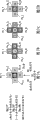
Described cmos image sensor 2 according to first execution mode has the dot structure of wherein using described pixel technology of sharing.Fig. 4 A illustrates three typical arrangement patterns sharing pixel to 4C.
Shown the Pareto diagram of the described shared pixel in the described cmos image sensor 2 in the epimere (upper lines) of 4C at Fig. 4 A.The a plurality of pixels that are connected with thick line are represented described shared pixel.
Shown the identifier (be called afterwards and share pixel ID) of each pixel position in the Pareto diagram in described shared pixel in the stage casing (medium lines) of 4C at Fig. 4 A.
Shown the order of representing by described shared pixel ID in the hypomere (lower lines) of 4C at Fig. 4 A from the pixel of described cmos image sensor 2 outputs.The output of graphic described shared pixel ID order only is primarily focused on the Pareto diagram of described shared pixel in described hypomere, does not consider the colour filter corresponding with described pixel at Fig. 4 A in the example of 4C.
Fig. 4 A illustrates two pixels conducts that wherein will be perpendicular to one another adjacent and shares the situation that pixel is handled.Specifically, two pixels that are arranged vertically on two adjacent levels are capable are handled as shared pixel.Therefore, for each horizontal line, " 0 " and " 1 " alternately occurs as sharing pixel ID, as shown in the stage casing.All pixels in pixel output order in a horizontal line all have shared pixel ID " 0 ", and all pixels in pixel output order in next horizontal line have shared pixel ID " 1 ", as shown in the hypomere.
Fig. 4 B also illustrates two pixels conducts that wherein will be perpendicular to one another adjacent and shares the situation that pixel is handled.Yet in the Pareto diagram of Fig. 4 B, a pair of shared pixel has moved a vertical pixel from following a pair of shared pixel.Therefore, " 0 " and " 1 " alternately occurs in each horizontal line as sharing pixel ID, in a horizontal line appearance of " 0 " and " 1 " in proper order with next horizontal line in opposite, as shown in the stage casing.Similarly, by sharing pixel that pixel ID represents along going out in the order, " 0 " and " 1 " alternately occurs in each horizontal line, in a horizontal line appearance of " 0 " and " 1 " in proper order with next horizontal line in opposite, as shown in the hypomere.
Fig. 4 C illustrates wherein the situation that will handle as shared pixel with four neighbors that " it " font is arranged.Therefore, for per four horizontal line " 0 ", " 1 ", " 2 " and " 3 " alternately occur as sharing pixel ID, as shown in the stage casing.Similarly, by sharing in the pixel output order that pixel ID represents, for per four horizontal line " 0 ", " 1 ", " 2 " and " 3 " are appearance alternately, as shown in the hypomere.
In the described cmos image sensor 2 of first execution mode, can adopt any Pareto diagram of Fig. 4 A to the shared pixel shown in the 4C according to the present invention.The Pareto diagram that the described cmos image sensor 2 of supposition has the shared pixel shown in Fig. 4 A in first execution mode.
Return with reference to Fig. 1, the light that incides on the optical unit 1 is exported through opto-electronic conversion and as the signal of telecommunication (being captive view data) in having the described cmos image sensor 2 of above-mentioned structure.Described cmos image sensor 2 is opened in response to the control signal of supplying with from described camera control microcomputer 5 or is stopped to read and control and reading the position of pixel data.
The described view data of exporting from described cmos image sensor 2 by a passage supplies to described analogy signal processing unit 3, and wherein said view data for example keeps and automatic gain control through over-sampling.Then, described view data is changed through analog to digital (A/D) in described analogy signal processing unit 3, and described digital signal is supplied to described digital signal processing unit 4.
Although in the superincumbent description, change through described sampling maintenance, automatic gain control and A/D described analogy signal processing unit 3 from the analog signal of described cmos image sensor 2 outputs, but the structure of described analogy signal processing unit 3 can be combined in the described cmos image sensor 2.
Described digital signal processing unit 4 will be converted to digital pixel data and in response to the instruction of controlling microcomputer 5 from described camera the described digital pixel data that is produced by described conversion be carried out various signal processing from the captive view data RAW (undressed data) that described analogy signal processing unit 3 is supplied with.The described various signal processing of carrying out in described digital signal processing unit 4 comprise so-called camera signal processing, as white balance, gamma-corrected and color difference signal are handled, and the calculation process that is used for camera control detection data (with the captive image-related data on the screen, as brightness, contrast and colourity).
Described digital signal processing unit 4 comprises the benchmark clock signal generating unit of the various clock signals of generation as described below (being timing signal).Described clock signal comprises horizontal-drive signal HD and the vertical synchronizing signal VD that is used for described captive view data.Described digital signal processing unit 4 is that described cmos image sensor 2 is supplied with described horizontal-drive signal HD, described vertical synchronizing signal VD and other essential clock signals.Described clock signal from the described benchmark clock signal generating unit in the described digital signal processing unit 4 also supplies to described camera control microcomputer 5.
In order to pass through the read method shown in Fig. 3 from each pixel reads pixel data, described cmos image sensor 2 is provided with reader and reads pulse signal generator.Described in the described cmos image sensor 2 read pulse signal generator and synchronously produces with described horizontal-drive signal HD that receives from described digital signal processing unit 4 and described vertical synchronizing signal VD and read clock signal, and according to the control signal of supplying with from described camera control microcomputer 5 from described cmos image sensor 2 reads pixel data.
According to first execution mode of the present invention, consider and share the described inhomogeneous of pixel that described digital signal processing unit 4 also comprises the shared pixel pixel mixing correction portion that is used to revise described pixel mixing.To describe described shared pixel pixel below in detail and mix correction portion.
Described camera control microcomputer 5 is determined the state of current captive image by the detection data of supplying with from described digital signal processing unit 4 with from image pick-up device 10 relevant camera shake information described camera shake transducer 6 supplies and described, thereby controls described image pick-up device 10 according to the various setting patterns of supplying with by described people interface microcomputer 8.Specifically, described camera control microcomputer 5 is supplied with for described cmos image sensor 2 and is read regional specific data, for the image control data is caught in described digital signal processing unit 4 supplies, for described lens driving unit 7 is supplied with the lens control data, for described analogy signal processing unit 3 is supplied with the gain control data that is used for described automatic gain control.
Described cmos image sensor 2 in response to described read clock signal read continuously with in the image capture area of described cmos image sensor 2 by the described corresponding signal in specific region that reads regional specific data appointment, and the described signal that reads supplied to described analogy signal processing unit 3.
Described digital signal processing unit 4, described lens driving unit 7 and described analogy signal processing unit 3 carry out and control the corresponding processing of controlling value that microcomputer 5 is supplied with from described camera, thus the signal processing of realizing ideal, clock signal generation, lens driving and gain controlling.
User interface elements 9 comprises that reception is by the button operation portion of the operation of user input with wherein show the pattern of described image pick-up device 10 and the display device of camera information.For example, via user interface elements 9, by people interface microcomputer 8 control users' actions menu.
People interface microcomputer 8 detects the image capture mode of the current selection of user or the control that the user wants according to the instruction that the user imports by user interface elements 9, and testing result is controlled microcomputer 5 as the user instruction information providing to described camera.
Thereby, described camera control microcomputer 5 is supplied with the camera control information (range-to-go, F number, shutter speed and enlargement ratio) that is obtained for people interface microcomputer 8, and indicates current camera information by the display device of user interface elements 9 to the user.Because they and the present invention do not have direct relation, so omit the detailed description of these assemblies here.
Fig. 5 is the block diagram of example that shows in detail the structure of described digital signal processing unit 4.In example shown in Figure 5, described digital signal processing unit 4 comprises camera signal pretreatment portion 41, shares pixel pixel mixing correction portion 42, camera signal master's handling part 43, benchmark clock signal generating unit 44 and communication interface portion 45.
Described benchmark clock signal generating unit 44 produces aforesaid horizontal-drive signal HD and vertical synchronizing signal VD, thereby described horizontal-drive signal HD that will produce and described vertical synchronizing signal VD supply to described cmos image sensor 2, and are that described camera signal pretreatment portion 41 and described shared pixel pixel are mixed the benchmark clock signal TG that correction portion 42 is supplied with as pixel sequential benchmark.In addition, described benchmark clock signal generating unit 44 is that described camera signal master's handling part 43 is supplied with various clock signals.Although do not illustrate among Fig. 5, described benchmark clock signal generating unit 44 also is that described camera control microcomputer 5 is supplied with various clock signals.
Described communication interface portion 45 is that described camera control microcomputer 5 is supplied with the various detected value DET that supply with from described camera signal master's handling part 43.Described camera control microcomputer 5 according to the various detected value DET that receive produce control signals (as automatic gaining controling signal) and with as described in control signal supply to corresponding processing unit.
In addition, described communication interface portion 45 receives camera signal processing controls parameters and be that described camera signal pretreatment portion 41, described shared pixel pixel are mixed correction portion 42 and the essential control signal of described camera signal master's handling part 43 supplies from described camera control microcomputer 5.Therefore, mix the processing operation of correction portion 42 and described camera signal master's handling part 43 by the described camera signal pretreatment portion 41 of described camera control microcomputer 5 controls, described shared pixel pixel.
Described camera signal pretreatment portion 41 receives the view data RAW that catches from described analogy signal processing unit 3, to carry out mixing the necessary a series of processing of revising of preliminary treatment as described pixel, as digital clamper.Because do not have direct relation, so omit the detailed description of a series of processing of being undertaken by described camera signal pretreatment portion 41 here with the present invention.
Output from described camera signal pretreatment portion 41 supplies to described shared pixel pixel mixing correction portion 42.Described shared pixel pixel is mixed the pixel mixing that correction portion 42 is revised each shared pixel (each pixel with identical shared pixel ID).
By described communication interface portion 45 from described camera control microcomputer 5 be described shared pixel pixel mix correction portion 42 supply with top with reference to Fig. 4 A to the relevant information of the described shared pixel ID of 4C, promptly shared pixel ID set information Sid.In addition, as described below, mix correction portion 42 from described camera control microcomputer 5 for described shared pixel pixel by described communication interface portion 45 and supply with and be used for described pixel and mix one group of corrected parameter group (a group correction coefficient group) the S φ that revises.
Described camera control microcomputer 5 produces the pixel that is used for each shared pixel (each pixel with identical shared pixel ID) to be mixed the corrected parameter group (correction factor group) who revises and the described corrected parameter group that will produce and for example is stored in the memory of himself.Therefore, described one group of corrected parameter group (a described group correction coefficient group) S φ comprises a plurality of corrected parameter groups (a plurality of correction factor group) of the quantity corresponding with the quantity of sharing pixel.
Described shared pixel pixel is mixed correction portion 42 and is mixed and revise by using the corrected parameter group that selects from the described one group of corrected parameter group S φ that obtains via described communication interface portion 45 that the described view data RAW that catches that supplies with from described camera signal pretreatment portion 41 is carried out described pixel.Specifically, described shared pixel pixel is mixed correction portion 42 and is determined which to share pixel (discerning the shared pixel ID of described pixel) from the pixel that described camera signal pretreatment portion 41 is supplied with corresponding to according to described shared pixel ID set information Sid, and from described one group of corrected parameter group S φ, select to be used for the corrected parameter group (correction factor group) of described shared pixel, and mix and revise by using selected corrected parameter group (correction factor group) to carry out pixel according to described definite result.Then, described shared pixel pixel mixing correction portion 42 will supply to described camera signal master's handling part 43 through the described pixel data that described pixel mixing is revised.
Described camera signal master's handling part 43 is in response to via the control commands of described communication interface portion 45 from described camera control microcomputer 5, carrying out various camera signal of the prior art handles, as noise reduction, defect correction, go mosaic processing, white balance and conversion of resolution, and supply with brightness data Y and color data C for the video processing block (not shown) in downstream as dateout.Because do not have direct relation, so omit the detailed description of described camera signal master's handling part 43 here with the present invention.
Before the example of describing the structure that mixes correction portion 42 according to the described shared pixel pixel of first execution mode, the summary of mixing correction according to the pixel that is used for each shared pixel of first execution mode is described now with reference to Fig. 6.Described here to be used to revise the method that pixel mixes only be an example, and the modification method that pixel is mixed is not limited to a kind of method of describing with reference to Fig. 6.
As mentioned above, described pixel is mixed and is owing to should incide light on the object pixel and leak into the described object pixel neighbor on every side and should incide light on the neighbor from described object pixel and leak into and cause in the described object pixel.Therefore, in colour filter with the Bayer array shown in Fig. 2 A, suppose mixture of colours scope AR comprise object pixel Px_C (pixel that will revise: the pixel of in Fig. 6 A, surrounding) eight pixels on every side by circle, as shown in Fig. 6 A.Reference Fig. 6 A to the description illustrated of 6C the colour filter in the Bayer array shown in Fig. 2 A.
In eight pixels in mixture of colours scope AR, from described object pixel Px_C to the distance of with respect to described object pixel Px_C, arranging pixel in an inclined direction than from described object pixel Px_C to respect to described object pixel Px_C at the top, the distance of pixel Px_T, Px_B, Px_L and the Px_R (with reference to Fig. 6 B) on bottom, left side and right side
 Doubly.Therefore, the mixture of colours is to the height of the influence degree comparison rest of pixels (with reference to Fig. 6 B) of top, bottom, left side and right pixel Px_T, Px_B, Px_L and Px_R.Owing to this reason, arrange that with respect to described object pixel Px_C the mixture of colours of pixel in an inclined direction is considered to negligible, be not included in described pixel and mix in the description of revising.
Thereby in this example, attentiveness only focuses on respect to the pixel of the top of described object pixel Px_C, bottom, left side and right pixel Px_T, Px_B, Px_L and Px_R mixes, and the modification model below using is formed the circuit that reduces the mixture of colours:
When light with the amount corresponding with mixture of colours rate when described object pixel leaks into the described neighbor, be that described light quantity increases the light quantity of leaking from described object pixel.
When light with the amount corresponding with mixture of colours rate when described neighbor leaks into the described object pixel, deduct the light quantity that leaks into described object pixel from described light quantity.
In other words, because along with the difference between the rank of the rank of described object pixel and described neighbor increases, the amount of the mixture of colours increases, and mixes correction so carry out described pixel according to the difference between the rank of the rank of described object pixel and described neighbor.Although in Japanese unexamined publication application No.2007-142697, disclose this method that pixel is mixed of revising, but embodiments of the present invention and said method difference are, switch " corrected parameter " that is applied to described correction circuit for each shared pixel.
To mix correction by using update equation to describe above-mentioned pixel now.According to equation (1) can calculate described pixel mix revise after from the value Sig_c ' of the picture element signal of described object pixel Px_C, wherein represent by Sig_c from the value of the picture element signal of described object pixel Px_C, value from the picture element signal of top adjacent pixels Px_T is represented by Sig_t, value from the picture element signal of bottom adjacent pixels Px_B is represented by Sig_b, value from the picture element signal of left side adjacent pixels Px_L is represented by Sig_l, value from the picture element signal of right side adjacent pixels Px_R is represented by Sig_r, as shown in Fig. 6 B, and wherein said object pixel Px_C and described top, the bottom, left side and right side neighbor Px_T, Px_B, mixture of colours rate between Px_L and the Px_R is respectively by K_t, K_b, K_l and K_r represent, as shown in Fig. 6 C.
Sig_c′=Sig_c
+K_t(Sig_c-Sig_t)
+K_r(Sig_c-Sig_r)
+K_l(Sig_c-Sig_l)
+K_b(Sig_c-Sig_b) (1)
Mixture of colours rate K_t, K_b, K_l and K_r are corresponding to the corrected parameter (correction factor) that is used for described top, bottom, left side and right side neighbor Px_T, Px_B, Px_L and Px_R.In this example, be used for four corrected parameters (correction factor) K_t of described top, bottom, left side and right side neighbor Px_T, Px_B, Px_L and Px_R, K_b, K_l and K_r form one group.
When colour filter had described Bayer array, the pixel of using the pixel of the pixel that has been assigned with (configuration) red color filter, configuration blue color filter or disposing green color filter was as described object pixel.All neighbors around the pixel of described red color filter of configuration and the described blue color filter of configuration all dispose green color filter, as shown in Fig. 2 A.
On the contrary, the pixel of the described green color filter of configuration is divided into two types: (1) left and right sides adjacent pixels configuration red color filter, and top and bottom adjacent pixels configuration blue color filter, and (2) left and right sides adjacent pixels configuration blue color filter, and top and bottom adjacent pixels configuration red color filter.
Therefore, described object pixel can be divided into Fig. 7 A to four types shown in the 7D.With reference to Fig. 7 A to 7D, the pixel of configuration red color filter is represented by R, the pixel of configuration blue color filter is represented by B, configuration green color filter and the pixel with the left and right sides neighbor that wherein disposes red color filter represented by Gr, and configuration green color filter and the pixel with the left and right sides neighbor that wherein disposes blue color filter are represented by Gb.
Although each object pixel that is four types has been set mixture of colours rate K_t, K_b, K_l and K_r, but Fig. 7 A in the example shown in the 7D for for simplicity, suppose with any one mixture of colours rate K_t, K_b, K_l and K_r (provide identical mixture of colours characteristic) in an identical manner and carry out the mixture of colours in four types object pixel.In other words, no matter the type of object pixel how, is all used identical mixture of colours rate.
As mentioned above, in revising, the mixing of the pixel shown in the 7D should use the pixel that belongs to three horizontal line at Fig. 7 A.Therefore, the pixel that described below shared pixel pixel is mixed in the correction portion 42 is mixed in the correction, the signal of the horizontal line under the described object pixel is called target line signal Sig_HC (with reference to Fig. 7 A), and it is with respect to having postponed and a horizontal line time corresponding from described analogy signal processing unit 3 signal supplied.
To comprise that the signal with respect to the horizontal line of the described top pixel of described object pixel is called top row signal Sig_HT (with reference to Fig. 7 A), it is with respect to having postponed and two horizontal line time corresponding from described analogy signal processing unit 3 signal supplied.Comprise signal with respect to the horizontal line of the described bottom pixel of described object pixel with corresponding, and it is called bottom line signal Sig_HB (with reference to Fig. 7 A) from described analogy signal processing unit 3 signal supplied.
Signal from described object pixel has postponed and a pixel clock (1D) time corresponding with respect to the described target line signal Sig_HC shown in Fig. 7 A, wherein " D " expression and a retardation that pixel clock is corresponding.Signal from the pixel that is positioned at place, described object pixel left side has postponed with respect to described target line signal Sig_HC and two pixel clocks (2D) time corresponding.Signal from the pixel that is positioned at place, described object pixel right side is corresponding with described target line signal Sig_HC, and promptly postponing is zero (0D).
Signal from the pixel that is positioned at described object pixel upside place has postponed with respect to described top row signal Sig_HT and a pixel clock (1D) time corresponding.Signal from the pixel that is positioned at described object pixel downside place has postponed with respect to described bottom line signal Sig_HB and a pixel clock (1D) time corresponding.
Fig. 8 shows that in detail carrying out above-mentioned pixel mixes the block diagram that the described shared pixel pixel of revising is mixed the structure example of correction portion 42.Described shared pixel pixel mixing correction portion 42 is included as time-delay regulator 421, two vertical row synchronizers 422, the timing sequencer 423 of the described view data RAW setting of catching of main line signal, shares pixel correction parameter selector 424, communication interface 425 and pixel mixing corrector 426.
Described time-delay regulator 421 is given as main line signal and the described view data RAW that catches that supplies with from described camera signal pretreatment portion 41 increases by the following time, promptly should the time corresponding with the delay that causes by the processing in described timing sequencer 423 and described shared pixel correction parameter selector 424, mix and carry out the following pixel that is used for each shared pixel in the corrector 426 and mix the sequential of revising thereby be adjusted at described pixel.
Described two vertical row (promptly two vertical row) synchronizer 422 is from the described time-delay regulator 421 described signals of reception and synchronous output and three signals that horizontal line is corresponding, and it is essential that this signal mixes correction for described pixel.Described two vertical row synchronizers 422 comprise that each is all corresponding to two delay lines 4221 and 4222 of a horizontal line, as shown in Figure 8.Described delay line 4221 and 4222 each all comprise static RAM (SRAM).
Described two vertical row synchronizers 422, do not postpone and supply to described pixel to mix corrector 426 from the signal (with reference to Fig. 9 A) of described time-delay regulator 421 outputs, and in described delay line 4221, have the delay corresponding and supply to described pixel as target line signal Sig_HC (with reference to Fig. 9 B) and mix corrector 426 with horizontal line as bottom line signal Sig_HB (with reference to figure).In addition, the described target line signal Sig_HC from described delay line 4221 has the delay corresponding with another horizontal line and supplies to described pixel mixing corrector 426 as top row signal Sig_HT (with reference to Fig. 9 B) in described delay line 4222.With reference to Fig. 9 B, " H " expression and the corresponding data volume (or time span) of a horizontal line (a horizontal fragment) during 0H delay, 1H delay and 2H postpone.
Described pixel mix corrector 426 carry out the pixel that is used for each shared pixel described below mix revise and after revising the capable signal Sig_HC ' of export target (seeing Fig. 9 C), described target line signal Sig_HC ' with respect to the output delay of described time-delay regulator 421 with a horizontal line time corresponding.
Described timing sequencer 423 is according to the benchmark clock signal TG that supplies with from described benchmark clock signal generating unit 44 with by the described shared pixel ID set information Sid of described communication interface 425 from 5 supplies of described camera control microcomputer, produce selection control signal (the being called parameter select signal) SEL of the described corrected parameter that is used for each shared pixel based on described shared pixel ID, and the parameter select signal SEL that produces is supplied to described shared pixel correction parameter selector 424.
In addition, described timing sequencer 423 writes-reads control signal R/W for the SRAM in the described two vertical row synchronizers 422 supplies with.Although do not illustrate in Fig. 8, described timing sequencer 423 is each supply pixel clock CLK that described time-delay regulator 421, described two vertical row synchronizers 422, described shared pixel correction parameter selector 424, described communication interface 425 and described pixel are mixed corrector 426.
Described shared pixel correction parameter selector 424 receives described one group of corrected parameter group S φ by described communication interface 425 from described camera control microcomputer 5.The quantity of group in described one group of corrected parameter group S φ is corresponding to the quantity of described shared pixel.As mentioned above, described one group of corrected parameter group S φ comprise and described object pixel Px_C and described top, bottom, left side and right side neighbor Px_T, Px_B, Px_L and Px_R between described mixture of colours rate K_t, K_b, the corrected parameter group of K_l and K_r correspondence (described correction factor group is corresponding to the mixture of colours characteristic between described object pixel and described top, bottom, left side and the right side neighbor).Described corrected parameter group's quantity is corresponding to the quantity of described shared pixel.
Described shared pixel correction parameter selector 424 is in response to the described parameter select signal SEL that supplies with from described timing sequencer 423, according to mixing the described object pixel of correction in the corrector 426 corresponding to which pixel in the described shared pixel in described pixel, select one group of corrected parameter (group correction coefficient) from described one group of corrected parameter group S φ, and selected one group of corrected parameter is supplied to described pixel mixing corrector 426.
Figure 10 illustrates the structure example of described shared pixel correction parameter selector 424.Described shared pixel correction parameter selector 424 comprise be used to select with described object pixel and described top, bottom, left side and right side neighbor between four selectors 4241,4242,4243 and 4244 of the corresponding described corrected parameter group (described correction factor group) of mixture of colours characteristic.
For described selector 4241 supplies comprise K0_t, K2_t ..., the corrected parameter group of Kn_t is for described selector 4242 supplies comprise K0_b, K2_b, ..., the corrected parameter group of Kn_b is for described selector 4243 supplies comprise K0_l, K2_l ..., the corrected parameter group of Kn_l, for described selector 4244 supplies comprise K0_r, K2_r ..., the corrected parameter group of Kn_r.Described corrected parameter group's quantity equates (n+1:n is the integer more than or equal to) with the quantity of described shared pixel (n+1).In the graphic example of Figure 10, for described shared pixel correction parameter selector 424 is supplied with the described corrected parameter group who is used for described top, bottom, left side and right side neighbor.
Described parameter select signal SEL supplies to each selector 4241,4242,4243 and 4244 from described timing sequencer 423.
In the above construction, corresponding with which pixel in the described shared pixel according to mixing the described object pixel of revising in the corrector 426 in described pixel, described corrected parameter is selected and extracted to each selector 4241,4242,4243 and 4244.In other words, from each selector 4241,4242,4243 and the 4244 outputs described corrected parameter corresponding with the described shared pixel ID of described object pixel.
The described corrected parameter that extracts from selector 4241,4242,4243 and 4244 is respectively by Ki_t, Ki_b, and Ki_l and Ki_r represent.Corrected parameter Ki_t, Ki_b, " i " among Ki_l and the Ki_r for example represent that described object pixel is an i pixel since a frame." i " have with describe below in identical implication.
The one group of corrected parameter φ i (i.e. the corrected parameter Ki_t that extracts from described shared pixel correction parameter selector 424, Ki_b, Ki_l and Ki_r) that is used for described object pixel supplies to described pixel and mixes corrector 426.
Described pixel is mixed corrector 426 and is used the one group of corrected parameter φ i that receives to carry out above-mentioned pixel mixing correction.Specifically, described pixel is mixed corrector 426 goes out object pixel and top, bottom, left side and the right side relevant with described object pixel from the signal extraction by the synchronous triplex row of described two vertical row synchronizers 422 neighbor, and use corrected parameter Ki_t, Ki_b, Ki_l and Ki_r carry out described corrected Calculation to the signal from the extraction pixel.
According to first execution mode, be that described pixel is mixed corrector 426 supply correction on-off control signal SW from described camera control microcomputer 5 by described communication interface 425.Described pixel is mixed corrector 426 in response to described correction on-off control signal SW, mixes the situation revised and does not carry out described pixel and mix between the situation of correction and switch carrying out described pixel.
Figure 11 is the block diagram that shows the structure example of described pixel mixing corrector 426.With reference to Figure 11, described pixel is mixed corrector 426 and is comprised four delay circuits 4261 that are used to postpone with a pixel clock time corresponding, 4262,4263 and 4265, be used to postpone mix and revise arithmetic processor 4266 with delay circuit 4264 of two pixel clock time corresponding and pixel.
Described target line signal Sig_HC supplies to described delay circuit 4261 from described two vertical row synchronizers 422, to postpone and a pixel clock time corresponding.Export described revise goal picture element signal Sig_c from described delay circuit 4261, and it is supplied to described pixel mixing correction arithmetic processor 4266.
Described top row signal Sig_HT supplies to described delay circuit 4262 from described two vertical row synchronizers 422, to postpone and a pixel clock time corresponding.Export described top pixel signal Sig_t from described delay circuit 4262, and it is supplied to described pixel mixing correction arithmetic processor 4266.
Described bottom line signal Sig_HB supplies to described delay circuit 4263 from described two vertical row synchronizers 422, to postpone and a pixel clock time corresponding.Export described bottom pixel signal Sig_b from described delay circuit 4263, and it is supplied to described pixel mixing correction arithmetic processor 4266.
Described target line signal Sig_HC supplies to described delay circuit 4264 from described two vertical row synchronizers 422, to postpone and two pixel clock time corresponding.Export described left pixel signal Sig_l from described delay circuit 4264, and it is supplied to described pixel mixing correction arithmetic processor 4266.
Because described right pixel signal Sig_r does not postpone,, described target line signal Sig_HC mixes correction arithmetic processor 4266 so supplying to described pixel from described two vertical row synchronizers 422.
Described one group of corrected parameter φ i supplies to described delay circuit 4265, to postpone and a pixel clock time corresponding.As the result who postpones, described object pixel (pixel that will revise) is synchronous with described one group of corrected parameter φ i, supplies to described pixel with the synchronous described one group of corrected parameter φ i of described object pixel and mixes correction arithmetic processor 4266.Although at delay circuit 4265 shown in the example shown in Figure 11, because described one group of corrected parameter φ i comprises four corrected parameter Ki_t, Ki_b, Ki_l and Ki_r are so in fact described delay circuit 4265 is made up of four delay circuits.
Figure 12 illustrates the example that described pixel is mixed the structure of revising arithmetic processor 4266.With reference to Figure 12, described pixel is mixed and is revised arithmetic processor 4266 and comprise subtraction circuit 501,502, and 503 and 504, multiplier circuit 511,512,513 and 514, adder circuit 521 and selector 522.
Described subtraction circuit 501 calculates the difference between described revise goal picture element signal Sig_c and the described top pixel signal Sig_t and described difference is supplied to described multiplier circuit 511.Described multiplier circuit 511 is multiplied by the described corrected parameter Ki_t that is used for described top neighbor of supply with the difference between described revise goal picture element signal Sig_c and the described top pixel signal Sig_t, and multiplied result is supplied to described adder circuit 521.
Described subtraction circuit 502 calculates the difference between described revise goal picture element signal Sig_c and the described right pixel signal Sig_r and described difference is supplied to described multiplier circuit 512.Described multiplier circuit 512 is multiplied by the described corrected parameter Ki_r that is used for described right side neighbor of supply with the difference between described revise goal picture element signal Sig_c and the described right pixel signal Sig_r, and multiplied result is supplied to described adder circuit 521.
Described subtraction circuit 503 calculates the difference between described revise goal picture element signal Sig_c and the described left pixel signal Sig_l and described difference is supplied to described multiplier circuit 513.Described multiplier circuit 513 is multiplied by the described corrected parameter Ki_l that is used for described left side neighbor of supply with the difference between described revise goal picture element signal Sig_c and the described left pixel signal Sig_l, and multiplied result is supplied to described adder circuit 521.
Described subtraction circuit 504 calculates the difference between described revise goal picture element signal Sig_c and the described bottom pixel signal Sig_b and described difference is supplied to described multiplier circuit 514.Described multiplier circuit 514 is multiplied by the described corrected parameter Ki_b that is used for described bottom neighbor of supply with the difference between described revise goal picture element signal Sig_c and the described bottom pixel signal Sig_b, and multiplied result is supplied to described adder circuit 521.
Described revise goal picture element signal Sig_c directly supplies to described adder circuit 521.Described adder circuit 521 is added to signal supplied together, thereby produces output signal Sig_c ' (being the result of calculation of equation (1)), and described output signal Sig_c ' is supplied to described selector 522.
Described correction on-off control signal SW supplies to described selector 522 by described communication interface 425 from described camera control microcomputer 5.When described correction activates, mix the output signal Sig_c ' that corrected Calculation causes by described pixel from described exciter circuit 521 from described selector 522 outputs.When described correction does not activate, so control described selector 522, promptly it is exported described revise goal picture element signal Sig_c and is not carried out described correction.
Do not take place therein in the situation of the image pickup device that pixel mixes, in described correction on-off control, do not activate described pixel and mix to revise and for example be easy to prevent disadvantageous correction.In addition, because as described in the above with reference to Figure 18 B, described pixel can not take place when described aperture is enough narrow probably mix, so in this case described pixel is mixed Correction and Control for not activating.
In described correction on-off control, when described correction does not activate, replace the switching of the selector 522 in the example as shown in figure 12, the value of all corrected parameters all can be made as zero.
As mentioned above, according to first execution mode, can use the independent corrected parameter that is used for each shared pixel to carry out described correction, following advantage is provided simultaneously, can be by the correction of described communication interface from the described pixel mixing of described external camera control microcomputer 5 controls is in real time revised, and can pass through at corrected parameter Ki_t, Ki_b, switch between Ki_l and the Ki_r, realize with respect to the directivity of described object pixel (pixel that will revise) that described pixel is mixed with described neighbor and revise, as described in the Japanese unexamined publication application No.2007-142697.Therefore, have a following advantage, promptly in the image pickup device that adopts described pixel technology of sharing, also can realize suitable pixel mixing correction.
Second execution mode
According to above-mentioned first execution mode, with the directivity of described neighbor with respect to described object pixel (pixel that will revise), use described top, bottom, left side and right side corrected parameter Ki_t, Ki_b, Ki_l and Ki_r realize described pixel mixing correction.In the graphic example of Figure 12, for each block of pixels, described pixel mixing correction arithmetic processor 4266 walks abreast simultaneously and carries out the calculating of described top, bottom, left side and right pixel.Four multiplier circuits (for example, also supposition wherein the situation by a plurality of pixels of a plurality of passages while parallel processings) are provided therefore, must be basically for each passage.In addition, must in described shared pixel correction parameter selector 424, four selectors be set.
Figure 13 has shown the situation of almost not finding directivity in the pixel mixed characteristic between described object pixel Px_C and described top, bottom, left side and right side neighbor Px_T, Px_B, Px_L and Px_R wherein, therefore, corrected parameter Ki_t=Ki_b=Ki_l=Ki_r=Ki_cm, wherein Ki_cm represents not have the public corrected parameter of directivity.
In this case, because mix public corrected parameter Ki_cm of use in the correction with the pixel between described top, bottom, left side and right side neighbor Px_T, Px_B, Px_L and the Px_R at described object pixel Px_C, so can reduce the size that described pixel is mixed corrector 426.For example, provide a multiplier circuit just enough.
Second execution mode of the present invention is applied in the situation that wherein circuit size reduces.Figure 14 illustrates the structure example according to the described shared pixel correction parameter selector 424 of second execution mode.
As shown in Figure 14, as the corrected parameter group in second execution mode, camera control microcomputer 5 produces a plurality of common parameter K0_cms corresponding with described pixel share I D, K1_cm ..., Kn_cm is just enough.
Described shared pixel correction parameter selector 424 comprises a selector 4245.Described a plurality of common parameter K0_cm, K1_cm ..., Kn_cm supplies to described selector 4245 by described communication interface 425 from described camera control microcomputer 5.
With the same in first execution mode, control described selector 4245 in response to the described parameter select signal SEL that supplies with from described timing sequencer 423, thereby output is suitable for the described public corrected parameter Ki_cm of the described revise goal pixel corresponding with each shared pixel ID.
Figure 15 shows the block diagram that mixes the structure example of revising arithmetic processor 4266 according to the described pixel of second execution mode.With reference to Figure 15, mixing in the correction arithmetic processor 4266 according to the described pixel of second execution mode, will be in adder circuit 523 from described subtraction circuit 501,502,503 add and are in the same place with the differences of 504 outputs, and addition result is supplied to public multiplier circuit 515.
According to second execution mode, described public corrected parameter Ki_cm from described shared pixel correction parameter selector 424 supplies to described public multiplier circuit 515, the addition result in the described adder circuit 523 be multiply by described public corrected parameter Ki_cm in described public multiplier circuit 515.Multiplication result in the described public multiplier circuit 515 supplies to described adder circuit 521, described multiplication result is added to described revise goal picture element signal Sig_c in described adder circuit 521.As a result, in described adder circuit 521, produce output signal Sig_c ' (being the result of calculation of equation (2)), and described output signal Sig_c ' is supplied to described selector 522.
Sig_c’=Sig_c
+Ki_cm×[(Sig_c-Sig_t)
+K_r(Sig_c-Sig_r)
+K_l(Sig_c-Sig_l)
+K_b(Sig_c-Sig_b)] (2)
Construct remaining assembly in the mode identical with first execution mode.
According to second execution mode, in described pixel mixing correction arithmetic processor 4266, use a multiplier circuit to realize described pixel mixing correction, and lost the flexibility that in the directivity of the neighbor relevant, relates to described object pixel (pixel that will revise).Therefore, for example during the directivity of the mixture of colours in ignoring imageing sensor, very effective according to the circuit structure of second execution mode, thus obtain desirable picture quality.
As mentioned above, according to top execution mode, by give and the adjacent or close pixel of described target between the described solid-state image pickup (no matter how sharing pattern, colour filter coding and fetch channel pattern) shared such as the so necessary circuit of dot structure of transistor use very simple structure, " the pixel mixed characteristic inhomogeneous " that can revise that the inhomogeneities of circuit arrangement between that general pattern owing to described solid-state image pickup causes, neighbor causes, thus the pixel sensitivity degree improved.
Other execution modes and modification
Although realized pixel mixing correction, can realize described pixel mixing correction by the software in the microcomputer by the hardware in the top execution mode.For example, Figure 16 is the flow chart of the example of software for display processing.
With reference to Figure 16, in step S101, described microcomputer obtains the pixel data about revise goal pixel and described top, bottom, left side and the right side neighbor relevant with described revise goal pixel.
In step S102, described microcomputer is with reference to described one group corrected parameter mass selection select and acquisition with described shared pixel ID corresponding described corrected parameter group or the public corrected parameter of shared pixel ID from producing in advance of described revise goal pixel.
In step S103, described microcomputer carries out described pixel mixing correction calculation process by use the described corrected parameter group who selects about the pixel data of described revise goal pixel and described top, bottom, left side and right side neighbor and in step S102 and obtain or the described public corrected parameter that obtain in step S101.Then, stop described software processes.
Although with reference to the case description in the top execution mode method of color filters arranged, fetch channel and shared pixel in the described solid-state image pickup, the present invention is not limited to described example.The present invention can use various examples, as long as they within the scope of the invention.
For example, in the example shown in the 4C, in the pixel output order of representing by described shared pixel ID, do not consider the color of colour filter at Fig. 4 A.Yet, when considering the color of color filters arranged in described solid-state image pickup, just become Figure 17 A to the example shown in the 17C to shared pixel ID described in three examples of the Pareto diagram of the shared pixel shown in the 4C with by the described pixel output order that described shared pixel ID represents at Fig. 4 A.
Specifically, at Figure 17 A, three examples of the Pareto diagram of the shared pixel in the epimere among 17B and the 17C have at the shared pixel ID shown in the stage casing.From described three examples output of Pareto diagram in the pixel output order of representing by described shared pixel ID shown in the hypomere.
In this case, select and corresponding corrected parameter group or the public corrected parameter of shared pixel ID shown in the stage casing of Figure 17 A in the 17C, and with the described pixel output sequence synchronization shown in the hypomere of Figure 17 A in the 17C revise.
Although in the multiplication that mixes the corrected parameter in the correction arithmetic processor 4266 according to the described pixel of first and second execution modes, use multiplier, can realize described multiplication by displacement structure.Select to use multiplier or in the displacement structure, realize multiplication according to accuracy of revising and the balance between the circuit size.
Although in the superincumbent execution mode, on across the whole screen of imageing sensor, use identical corrected parameter group to be used for the described pixel mixing correction of each shared pixel, but also have following situation, the characteristic that promptly wherein is used for each shared pixel is also non-constant on whole screen.For example, different in the characteristic in the screen center zone and the screen peripheral zone.
In this case, be provided for the corrected parameter group in described screen center zone and be used for the corrected parameter group of its outer peripheral areas, and for example exist in the memory.Be arranged in the central area of described screen or be arranged in the testing result of its outer peripheral areas according to described revise goal pixel, switch described corrected parameter group.
Although in the superincumbent description, described camera control microcomputer 5 produces described corrected parameter group in advance, thereby described corrected parameter group is stored in oneself the memory and supplies with described corrected parameter groups for described shared pixel correction parameter selector 424, but replace the described corrected parameter group of storage, described camera control microcomputer 5 can supply to described shared pixel correction parameter selector 424 with described corrected parameter group when producing described corrected parameter group.
Although the description illustrated of the structure in first to the 3rd execution mode shared pattern of pixels and the read method shown in Fig. 4 A, but it is desirable to, for example described timing sequencer 423 can be programmed, thereby can support other shared pattern of pixels and read methods.
Although for example understand described solid-state image pickup by cmos image sensor in the superincumbent execution mode, described solid-state image pickup can be a ccd image sensor.
It will be appreciated by those skilled in the art that according to designing requirement and other factors, can carry out various modifications, combination, recombinant and replacement, as long as they drop in the scope of claims and equivalent thereof.
Claims (6)
1. image pick-up device comprises:
Solid-state image pickup is configured to share the necessary circuit of dot structure between a plurality of pixels of forming each group, and described a plurality of pixels are arranged with two-dimensional array, the described group of pixel with aligned identical pattern that comprises specific quantity;
Pixel is mixed correcting part, is used for should inciding on each pixel of described solid-state image pickup according to corrected parameter correction that the light that leaks into the described pixel leaks but the light of the neighbor around from described pixel leaks to described pixel leaks and/or should incide on the described neighbor;
The corrected parameter production part is used to produce a plurality of corrected parameters corresponding with described a plurality of pixels of forming described group; With
The corrected parameter alternative pack, according to the pixel that will mix the correcting part correction by described pixel corresponding to which pixel of forming in described a plurality of pixels of described group, select corrected parameter from described a plurality of corrected parameters that described corrected parameter production part is supplied with, and the corrected parameter of selecting is supplied to described pixel mixing correcting part.
2. image pick-up device according to claim 1, wherein said pixel mix value and described corrected parameter revise that for described a plurality of neighbors the produce described pixel that will revise of correcting part by using a plurality of neighbors around the described pixel that will revise.
3. image pick-up device according to claim 1, wherein said pixel mix correcting part by the value of using the described pixel a plurality of neighbors on every side that will revise and the described pixel that general corrected parameter correction will be revised for described a plurality of neighbors.
4. the method for catching view data of a correction in being provided with the image pick-up device of solid-state image pickup, described solid-state image pickup is configured to share the necessary circuit of dot structure between a plurality of pixels of forming each group, described a plurality of pixel is arranged with two-dimensional array, described group of pixel that comprises specific quantity with aligned identical pattern, described method comprises:
According to the pixel that will revise corresponding to which pixel of forming in described a plurality of pixels of described group, select corrected parameters from a plurality of corrected parameters corresponding with described a plurality of pixels of forming described group, described corrected parameter is used for revising on each pixel that should incide described solid-state image pickup that the light that leaks into the described pixel leaks but the light of the neighbor around from described pixel leaks to described pixel leaks and/or should incide on the described neighbor; And
Receive described corrected parameter of selecting and the described pixel that will revise according to described corrected parameter correction.
5. computer-readable program that is used to be provided with the image pick-up device of solid-state image pickup, described solid-state image pickup is configured to share the necessary circuit of dot structure between a plurality of pixels of forming each group, described a plurality of pixel is arranged with two-dimensional array, described group of pixel that comprises specific quantity with aligned identical pattern, described program comprises:
Which be used for according to the pixel that will revise corresponding to the pixel of forming described a plurality of pixels of described group, the light that leaks into the described pixel leaks but the light of the neighbor around from described pixel leaks to described pixel leaks and/or should incide on the described neighbor to select the computer executable instructions of corrected parameters, described corrected parameter to be used for revising on each pixel that should incide described solid-state image pickup from a plurality of corrected parameters corresponding with described a plurality of pixels of forming described group; With
The computer executable instructions of the described pixel that is used to receive the described corrected parameter of selection and will revises according to described corrected parameter correction.
6. image pick-up device comprises:
Solid-state image pickup is configured to share the necessary circuit of dot structure between a plurality of pixels of forming each group, and described a plurality of pixels are arranged with two-dimensional array, the described group of pixel with aligned identical pattern that comprises specific quantity;
Pixel is mixed amending unit, is configured to should incide on each pixel of described solid-state image pickup according to corrected parameter correction that the light that leaks in the described pixel leaks but the light the neighbor around from described pixel leaks to described pixel leaks and/or should incide on the described neighbor;
The corrected parameter generation unit is configured to produce a plurality of corrected parameters corresponding with described a plurality of pixels of forming described group; With
The corrected parameter selected cell, which be configured to according to the pixel that will mix the amending unit correction by described pixel corresponding to the pixel of forming in described a plurality of pixels of described group, select corrected parameter from described a plurality of corrected parameters that described corrected parameter generation unit is supplied with, and the corrected parameter of selecting is supplied to described pixel mixing amending unit.
Applications Claiming Priority (2)
| Application Number | Priority Date | Filing Date | Title |
|---|---|---|---|
| JP2007293875A JP5045380B2 (en) | 2007-11-13 | 2007-11-13 | Imaging apparatus, imaging data correction method, and program |
| JP2007293875 | 2007-11-13 |
Publications (1)
| Publication Number | Publication Date |
|---|---|
| CN101437166A true CN101437166A (en) | 2009-05-20 |
Family
ID=40415854
Family Applications (1)
| Application Number | Title | Priority Date | Filing Date |
|---|---|---|---|
| CNA2008101727249A Pending CN101437166A (en) | 2007-11-13 | 2008-11-11 | Image pickup apparatus, method of correcting captured image data, and program |
Country Status (6)
| Country | Link |
|---|---|
| US (1) | US8035709B2 (en) |
| EP (1) | EP2061231A3 (en) |
| JP (1) | JP5045380B2 (en) |
| KR (1) | KR20090049540A (en) |
| CN (1) | CN101437166A (en) |
| BR (1) | BRPI0804843A2 (en) |
Cited By (8)
| Publication number | Priority date | Publication date | Assignee | Title |
|---|---|---|---|---|
| CN102124744A (en) * | 2009-06-30 | 2011-07-13 | 索尼公司 | Image processing device, image processing method, imaging device, and computer program |
| CN102696228A (en) * | 2010-10-04 | 2012-09-26 | 富士胶片株式会社 | Imaging apparatus and color contamination correction method |
| CN103024305A (en) * | 2012-12-27 | 2013-04-03 | 上海集成电路研发中心有限公司 | Improved pixel array |
| CN103597821A (en) * | 2011-07-13 | 2014-02-19 | 富士胶片株式会社 | Image pickup apparatus and signal value correction method |
| CN108881748A (en) * | 2017-05-10 | 2018-11-23 | 宝视纳股份公司 | Image processing apparatus and method, digital camera, computer equipment and program product |
| CN110581964A (en) * | 2013-10-31 | 2019-12-17 | 索尼半导体解决方案公司 | Solid-state imaging device, signal processing device, and electronic apparatus |
| CN111474893A (en) * | 2019-11-23 | 2020-07-31 | 田华 | Intelligent pixel array control system |
| CN115004680A (en) * | 2019-12-11 | 2022-09-02 | Lg伊诺特有限公司 | Image processing apparatus, image processing method, and program |
Families Citing this family (16)
| Publication number | Priority date | Publication date | Assignee | Title |
|---|---|---|---|---|
| JP4388909B2 (en) * | 2005-04-25 | 2009-12-24 | イーストマン コダック カンパニー | Pixel defect correction device |
| JP5045380B2 (en) * | 2007-11-13 | 2012-10-10 | ソニー株式会社 | Imaging apparatus, imaging data correction method, and program |
| JP5254762B2 (en) * | 2008-11-28 | 2013-08-07 | キヤノン株式会社 | Imaging apparatus, imaging system, and signal correction method in imaging apparatus |
| JP5402349B2 (en) * | 2009-07-23 | 2014-01-29 | ソニー株式会社 | Solid-state imaging device, driving method thereof, and electronic apparatus |
| US8619163B2 (en) * | 2009-09-18 | 2013-12-31 | Canon Kabushiki Kaisha | Solid state imaging using a correction parameter for correcting a cross talk between adjacent pixels |
| JP5526840B2 (en) | 2010-02-09 | 2014-06-18 | ソニー株式会社 | Image signal processing apparatus, imaging apparatus, image signal processing method, and program |
| JP5269016B2 (en) * | 2010-09-10 | 2013-08-21 | 株式会社東芝 | Image processing device |
| JP2012169830A (en) | 2011-02-14 | 2012-09-06 | Sony Corp | Image processing apparatus, image processing method, and electronic apparatus |
| CN103563360B (en) * | 2011-06-30 | 2015-03-11 | 富士胶片株式会社 | Imaging device and imaging method |
| WO2013100033A1 (en) * | 2011-12-28 | 2013-07-04 | 富士フイルム株式会社 | Image processing device and method, and imaging device |
| JP2015062264A (en) * | 2012-01-30 | 2015-04-02 | ソニー株式会社 | Solid-state imaging device, solid-state imaging apparatus, and image processing method |
| JP6087674B2 (en) * | 2013-02-27 | 2017-03-01 | キヤノン株式会社 | Imaging device |
| KR102174192B1 (en) * | 2014-01-14 | 2020-11-04 | 에스케이하이닉스 주식회사 | Timing generator based on processor and method thereof, and CMOS image sensor using that |
| JP6316043B2 (en) * | 2014-03-19 | 2018-04-25 | キヤノン株式会社 | Apparatus, method, and program |
| KR20150146308A (en) * | 2014-06-23 | 2015-12-31 | 삼성전자주식회사 | Image sensor and method of operating the image sensor |
| KR102301620B1 (en) * | 2015-02-02 | 2021-09-14 | 삼성전자주식회사 | Photographing apparatus and method for the light leakage correction |
Family Cites Families (24)
| Publication number | Priority date | Publication date | Assignee | Title |
|---|---|---|---|---|
| US5053615A (en) * | 1990-04-06 | 1991-10-01 | Samsung Electronics Co., Ltd. | Correction algorithm for contiguous CCD elements leakage |
| EP0845900B1 (en) | 1995-08-11 | 2002-11-06 | Kabushiki Kaisha Toshiba | Image system, solid-state imaging device semiconductor integrated circuit |
| JP3838665B2 (en) | 1995-08-11 | 2006-10-25 | 株式会社 東芝 | MOS type solid-state imaging device |
| JP4120020B2 (en) * | 1997-03-26 | 2008-07-16 | ソニー株式会社 | Solid-state imaging device |
| JPH11146409A (en) * | 1997-11-07 | 1999-05-28 | Minolta Co Ltd | Video camera |
| JP3498553B2 (en) * | 1997-11-10 | 2004-02-16 | ミノルタ株式会社 | Video camera |
| CN1316384C (en) | 2000-04-26 | 2007-05-16 | 电通应用股份有限公司 | Vehicle diagnostic system to reduce fuel consumption and emissions |
| WO2002063380A2 (en) * | 2001-02-06 | 2002-08-15 | Koninklijke Philips Electronics N.V. | Preventing green non-uniformity in image sensors |
| JP3988189B2 (en) | 2002-11-20 | 2007-10-10 | ソニー株式会社 | Solid-state imaging device |
| JP4207736B2 (en) | 2003-10-01 | 2009-01-14 | ソニー株式会社 | Solid-state imaging device |
| US7561194B1 (en) * | 2003-10-17 | 2009-07-14 | Eastman Kodak Company | Charge diffusion crosstalk reduction for image sensors |
| US7425933B2 (en) * | 2004-04-14 | 2008-09-16 | Samsung Semiconductor Israel R&D Center (Sirc) | Systems and methods for correcting green disparity in imager sensors |
| US7023451B2 (en) * | 2004-06-14 | 2006-04-04 | Sharp Laboratories Of America, Inc. | System for reducing crosstalk |
| JP4492250B2 (en) * | 2004-08-11 | 2010-06-30 | ソニー株式会社 | Solid-state image sensor |
| JP4971586B2 (en) | 2004-09-01 | 2012-07-11 | キヤノン株式会社 | Solid-state imaging device |
| JP2006121164A (en) * | 2004-10-19 | 2006-05-11 | Canon Inc | Imaging apparatus |
| US7656441B2 (en) * | 2005-01-05 | 2010-02-02 | Eastman Kodak Company | Hue correction for electronic imagers |
| JP4389865B2 (en) * | 2005-11-17 | 2009-12-24 | ソニー株式会社 | SIGNAL PROCESSING DEVICE FOR SOLID-STATE IMAGING ELEMENT, SIGNAL PROCESSING METHOD, AND IMAGING DEVICE |
| US8005297B2 (en) * | 2006-01-18 | 2011-08-23 | Qualcomm Incorporated | Method and apparatus for adaptive and self-calibrated sensor green channel gain balancing |
| JP4329765B2 (en) | 2006-01-31 | 2009-09-09 | ソニー株式会社 | Solid-state imaging device |
| JP4695552B2 (en) * | 2006-06-28 | 2011-06-08 | 富士フイルム株式会社 | Image processing apparatus and method |
| KR100866635B1 (en) * | 2006-09-25 | 2008-11-03 | 가부시키가이샤 히다치 고쿠사이 덴키 | Image pickup device and image pickup method |
| US7830428B2 (en) * | 2007-04-12 | 2010-11-09 | Aptina Imaging Corporation | Method, apparatus and system providing green-green imbalance compensation |
| JP5045380B2 (en) * | 2007-11-13 | 2012-10-10 | ソニー株式会社 | Imaging apparatus, imaging data correction method, and program |
-
2007
- 2007-11-13 JP JP2007293875A patent/JP5045380B2/en not_active Expired - Fee Related
-
2008
- 2008-11-05 EP EP08253602A patent/EP2061231A3/en not_active Withdrawn
- 2008-11-05 BR BRPI0804843-6A patent/BRPI0804843A2/en not_active IP Right Cessation
- 2008-11-07 KR KR1020080110574A patent/KR20090049540A/en not_active Application Discontinuation
- 2008-11-11 CN CNA2008101727249A patent/CN101437166A/en active Pending
- 2008-11-11 US US12/268,634 patent/US8035709B2/en not_active Expired - Fee Related
Cited By (16)
| Publication number | Priority date | Publication date | Assignee | Title |
|---|---|---|---|---|
| CN102124744A (en) * | 2009-06-30 | 2011-07-13 | 索尼公司 | Image processing device, image processing method, imaging device, and computer program |
| US10015424B2 (en) | 2009-06-30 | 2018-07-03 | Sony Corporation | Method and apparatus for eliminating crosstalk amount included in an output signal |
| CN102124744B (en) * | 2009-06-30 | 2014-04-02 | 索尼公司 | Image processing device, image processing method, imaging device, and computer program |
| US8890981B2 (en) | 2009-06-30 | 2014-11-18 | Sony Corporation | Method and apparatus for eliminating crosstalk amount included in an output signal |
| CN102696228A (en) * | 2010-10-04 | 2012-09-26 | 富士胶片株式会社 | Imaging apparatus and color contamination correction method |
| CN102696228B (en) * | 2010-10-04 | 2015-01-21 | 富士胶片株式会社 | Imaging apparatus and color contamination correction method |
| CN103597821A (en) * | 2011-07-13 | 2014-02-19 | 富士胶片株式会社 | Image pickup apparatus and signal value correction method |
| CN103597821B (en) * | 2011-07-13 | 2015-11-25 | 富士胶片株式会社 | Image pick up equipment and signal value bearing calibration |
| CN103024305B (en) * | 2012-12-27 | 2018-05-29 | 上海集成电路研发中心有限公司 | Improved pel array |
| CN103024305A (en) * | 2012-12-27 | 2013-04-03 | 上海集成电路研发中心有限公司 | Improved pixel array |
| CN110581964A (en) * | 2013-10-31 | 2019-12-17 | 索尼半导体解决方案公司 | Solid-state imaging device, signal processing device, and electronic apparatus |
| CN110581964B (en) * | 2013-10-31 | 2022-03-18 | 索尼半导体解决方案公司 | Image pickup device and electronic apparatus |
| CN108881748A (en) * | 2017-05-10 | 2018-11-23 | 宝视纳股份公司 | Image processing apparatus and method, digital camera, computer equipment and program product |
| CN108881748B (en) * | 2017-05-10 | 2022-07-01 | 宝视纳股份公司 | Image processing apparatus and method, digital camera, computer device, and program product |
| CN111474893A (en) * | 2019-11-23 | 2020-07-31 | 田华 | Intelligent pixel array control system |
| CN115004680A (en) * | 2019-12-11 | 2022-09-02 | Lg伊诺特有限公司 | Image processing apparatus, image processing method, and program |
Also Published As
| Publication number | Publication date |
|---|---|
| BRPI0804843A2 (en) | 2009-12-08 |
| EP2061231A2 (en) | 2009-05-20 |
| EP2061231A3 (en) | 2009-06-03 |
| US8035709B2 (en) | 2011-10-11 |
| US20090122165A1 (en) | 2009-05-14 |
| KR20090049540A (en) | 2009-05-18 |
| JP2009124282A (en) | 2009-06-04 |
| JP5045380B2 (en) | 2012-10-10 |
Similar Documents
| Publication | Publication Date | Title |
|---|---|---|
| CN101437166A (en) | Image pickup apparatus, method of correcting captured image data, and program | |
| US9942482B2 (en) | Image sensor with transfer gate control signal lines | |
| CN102883114B (en) | The driving method of solid state image pickup device, imaging system and solid state image pickup device | |
| JP2021093767A (en) | Image pickup device | |
| US8558925B2 (en) | Signal processing apparatus, image sensing apparatus, image sensing system, and signal processing method | |
| CN100546392C (en) | The signal processing apparatus of solid-state imager and signal processing method and camera head | |
| CN101715084B (en) | Solid-state imaging device, imaging apparatus, and ad conversion gain adjusting method | |
| US7399952B2 (en) | Image processing apparatus and image capturing apparatus | |
| CN101753863B (en) | Solid-state imaging device, method for processing signal of solid-state imaging device, and imaging apparatus | |
| TWI521965B (en) | Camera and camera methods, electronic machines and programs | |
| CN103369241B (en) | Picture pick-up device and signal processing method | |
| CN103748868A (en) | Imaging device, signal processing method, and program | |
| CN102224736A (en) | Image pick-up device | |
| KR20130038035A (en) | Image sensor | |
| TW200816824A (en) | Imaging device camera system and driving method of the same | |
| CN102959959B (en) | Solid-state imaging device driving method, solid state image pickup device and imaging device | |
| CN105516698A (en) | Imaging method of image sensor, imaging device and electronic device | |
| US20180278858A1 (en) | Imaging device and control method thereof, and electronic apparatus | |
| CN105516700A (en) | Imaging method of image sensor, imaging device and electronic device | |
| CN104041019A (en) | Imaging device, method for controlling imaging device, and control program | |
| CN100446547C (en) | Solid-state image sensor having its photosensitive cells broadened in area | |
| US11689823B2 (en) | Image sensing device and operating method thereof | |
| CN216873256U (en) | Image sensor for partially shielding phase focusing by shared micro-lens | |
| JP2009124524A (en) | Imaging apparatus, and captured pixel data correcting method and program | |
| CN104869331A (en) | Solid-state Imaging Apparatus And Camera System |
Legal Events
| Date | Code | Title | Description |
|---|---|---|---|
| C06 | Publication | ||
| PB01 | Publication | ||
| C10 | Entry into substantive examination | ||
| SE01 | Entry into force of request for substantive examination | ||
| C02 | Deemed withdrawal of patent application after publication (patent law 2001) | ||
| WD01 | Invention patent application deemed withdrawn after publication |
Open date: 20090520 |