CN101286703B - Method and apparatus for controlling the maximum output power of a power converter - Google Patents
Method and apparatus for controlling the maximum output power of a power converter Download PDFInfo
- Publication number
- CN101286703B CN101286703B CN2008101092202A CN200810109220A CN101286703B CN 101286703 B CN101286703 B CN 101286703B CN 2008101092202 A CN2008101092202 A CN 2008101092202A CN 200810109220 A CN200810109220 A CN 200810109220A CN 101286703 B CN101286703 B CN 101286703B
- Authority
- CN
- China
- Prior art keywords
- mains switch
- power inverter
- coupled
- current
- controller
- Prior art date
- Legal status (The legal status is an assumption and is not a legal conclusion. Google has not performed a legal analysis and makes no representation as to the accuracy of the status listed.)
- Expired - Fee Related
Links
Images


Classifications
-
- H—ELECTRICITY
- H02—GENERATION; CONVERSION OR DISTRIBUTION OF ELECTRIC POWER
- H02M—APPARATUS FOR CONVERSION BETWEEN AC AND AC, BETWEEN AC AND DC, OR BETWEEN DC AND DC, AND FOR USE WITH MAINS OR SIMILAR POWER SUPPLY SYSTEMS; CONVERSION OF DC OR AC INPUT POWER INTO SURGE OUTPUT POWER; CONTROL OR REGULATION THEREOF
- H02M3/00—Conversion of dc power input into dc power output
- H02M3/22—Conversion of dc power input into dc power output with intermediate conversion into ac
- H02M3/24—Conversion of dc power input into dc power output with intermediate conversion into ac by static converters
- H02M3/28—Conversion of dc power input into dc power output with intermediate conversion into ac by static converters using discharge tubes with control electrode or semiconductor devices with control electrode to produce the intermediate ac
- H02M3/325—Conversion of dc power input into dc power output with intermediate conversion into ac by static converters using discharge tubes with control electrode or semiconductor devices with control electrode to produce the intermediate ac using devices of a triode or a transistor type requiring continuous application of a control signal
- H02M3/335—Conversion of dc power input into dc power output with intermediate conversion into ac by static converters using discharge tubes with control electrode or semiconductor devices with control electrode to produce the intermediate ac using devices of a triode or a transistor type requiring continuous application of a control signal using semiconductor devices only
- H02M3/33507—Conversion of dc power input into dc power output with intermediate conversion into ac by static converters using discharge tubes with control electrode or semiconductor devices with control electrode to produce the intermediate ac using devices of a triode or a transistor type requiring continuous application of a control signal using semiconductor devices only with automatic control of the output voltage or current, e.g. flyback converters
- H02M3/33523—Conversion of dc power input into dc power output with intermediate conversion into ac by static converters using discharge tubes with control electrode or semiconductor devices with control electrode to produce the intermediate ac using devices of a triode or a transistor type requiring continuous application of a control signal using semiconductor devices only with automatic control of the output voltage or current, e.g. flyback converters with galvanic isolation between input and output of both the power stage and the feedback loop
-
- G—PHYSICS
- G05—CONTROLLING; REGULATING
- G05F—SYSTEMS FOR REGULATING ELECTRIC OR MAGNETIC VARIABLES
- G05F1/00—Automatic systems in which deviations of an electric quantity from one or more predetermined values are detected at the output of the system and fed back to a device within the system to restore the detected quantity to its predetermined value or values, i.e. retroactive systems
- G05F1/66—Regulating electric power
-
- H—ELECTRICITY
- H02—GENERATION; CONVERSION OR DISTRIBUTION OF ELECTRIC POWER
- H02M—APPARATUS FOR CONVERSION BETWEEN AC AND AC, BETWEEN AC AND DC, OR BETWEEN DC AND DC, AND FOR USE WITH MAINS OR SIMILAR POWER SUPPLY SYSTEMS; CONVERSION OF DC OR AC INPUT POWER INTO SURGE OUTPUT POWER; CONTROL OR REGULATION THEREOF
- H02M1/00—Details of apparatus for conversion
- H02M1/32—Means for protecting converters other than automatic disconnection
-
- H—ELECTRICITY
- H02—GENERATION; CONVERSION OR DISTRIBUTION OF ELECTRIC POWER
- H02M—APPARATUS FOR CONVERSION BETWEEN AC AND AC, BETWEEN AC AND DC, OR BETWEEN DC AND DC, AND FOR USE WITH MAINS OR SIMILAR POWER SUPPLY SYSTEMS; CONVERSION OF DC OR AC INPUT POWER INTO SURGE OUTPUT POWER; CONTROL OR REGULATION THEREOF
- H02M1/00—Details of apparatus for conversion
- H02M1/0003—Details of control, feedback or regulation circuits
- H02M1/0009—Devices or circuits for detecting current in a converter
Landscapes
- Engineering & Computer Science (AREA)
- Power Engineering (AREA)
- Physics & Mathematics (AREA)
- Electromagnetism (AREA)
- General Physics & Mathematics (AREA)
- Radar, Positioning & Navigation (AREA)
- Automation & Control Theory (AREA)
- Dc-Dc Converters (AREA)
- Inverter Devices (AREA)
Abstract
A controller for a power converter (100) and a method of controlling the power converter (100) is disclosed. An example circuit controller (115) according to aspects of the present invention includes an input voltage sensor (141) to be coupled to receive an input signal representative of an input voltage of the power converter. A current sensor (140) is also included and is to be coupled to sense a current flowing in a power switch (105). A drive signal generator (144) is to be coupled to drive the power switch (105) into an on state for an on time period and an off state for an off time period. The controller (115) is coupled to adjust a switching cycle period of the power switch (105) to be proportional to a value of input signal multiplied by a time period.; The time period is time it takes for the current flowing in the power switch (105) to change between two current values when the power switch is in the on state.
Description
Related application
The name that the application requires on April 6th, 2007 to propose is called the U.S. Provisional Application No.60/922 of " Method And Apparatus ForControlling The Maximum Output Power Of A Power Converter (method and apparatus that is used for the peak power output of power ratio control converter) ", 191 rights and interests.
Technical field
The present invention relates generally to power inverter, more specifically, the present invention relates to the output of Modulating Power converter.
Background technology
Many electronic equipments such as cell phone, personal digital assistant (PDA), kneetop computer etc. are by relatively low voltage DC Power supply.Because power is passed the power as high pressure AC by wall outlet usually, is low voltage DC power so need to be commonly called the device of power inverter with high pressure AC power conversion.Low voltage DC power can directly offer described device or it by power inverter and can be used to the rechargeable battery charging, and it provides energy for described device again, but just needs charging in case the energy of storage is consumed it.Usually, use to comprise that the battery charger of power inverter charges to battery, this power inverter satisfies the requirement of the needed constant current of battery and constant voltage.Other electronic equipment, such as DVD player, computer monitor, TV etc. also needs the power inverter for the device operation.Power inverter in these equipment also must provide output voltage and the electric current of the requirement of satisfying described device.In operation, power inverter can be regulated the power output that is delivered to electronic equipment with controller, and this electronic equipment for example is battery, and it is commonly called load.More specifically, in order to regulate the power that is transferred to described load, this controller can be coupled to the transducer of the feedback information of the output that power inverter is provided.This controller opens with the power of cutting out to be adjusted to load with the feedback information of response from transducer by the control mains switch, thereby will transfer to output from the energy pulse of the input power of for example power line.
The product of power inverter output voltage and electric current is known as the power output of power inverter.In most of power inverter is used, be necessary to limit the peak power output under the worst case, provide this peak power output can exempt from the destruction of excessive power delivery with the equipment of guaranteeing to be provided electric power.The peak power output tolerance of improving the power inverter transmission can be optimized to the electronic equipment that electric power is provided by power inverter to guarantee the safety operation under the failure condition, and has improved reliability of electronic equipment, has reduced the complete cost of electronic equipment.
A special type of operable power inverter is flyback power converter.In flyback power converter, energy transmission is isolated input and the output of power inverter conductively.Electricity isolation prevents that the DC electric current from flowing through between the input and output of power inverter.
Thereby flyback power converter by the Switching power switch produce output during the service time of mains switch in energy transmission stored energy, and transfer energy to power inverter output in the time at least a portion that mains switch is turned off.In the flyback converter of not isolation, still need energy transmission to store the energy that is delivered to power inverter output from the power inverter input, but need to do not isolated by the electricity that energy transmission provides.
In operation, power inverter can use the controller adjustment to be delivered to the power output of load.More specifically, the peak power output that this controller can the power-limiting converter with response by the output voltage of the output of sense power converter and or the feedback information that obtains of output current.Output place sensing output current at power inverter can reduce power inverter efficient usually, because usually can introduce resistive element to provide and the proportional voltage signal of output current of power converter.If the output current of power inverter is not sensed in power inverter output place, then the maximum power transfer restriction can be determined by the standard allowance of the particular elements in the power inverter.
The tolerance of the protective current limiting threshold value of the electric current that in this mains switch, flows when the tolerance of the inductance that two parts of the tolerance of its parameter influence maximum output power of power converter are energy transmission and mains switch are in on-state.The electric current that controller flows in this mains switch when can the sensing mains switch connecting, and maximum protection current limitation threshold value can be set.In this case, the tolerance of controller maximum protection current limitation threshold value will affect the tolerance of maximum output power of power converter.
Summary of the invention
According to one embodiment of present invention, provide a kind of controller for power inverter, comprising: input voltage sensor, it is coupled to receive the input signal of the input voltage that represents power inverter; Current sensor, it is coupled the electric current that flows with sensing in mains switch; And drive signal generator, its be coupled take the driving power switch cycle turn-on time as on-state and cycle turn-off time as off state, wherein this drive signal generator switching cycle period of being coupled to adjust mains switch make itself and input signal multiply by the electric current that when mains switch is in on-state, in mains switch, flows to change the value of used time between two current values proportional.
According to another embodiment of the invention, provide a kind of controller for power inverter, comprising: input voltage sensor, it is coupled to receive the input signal of the input voltage that represents this power inverter; Current sensor, it is coupled the electric current that flows with sensing in mains switch; And drive signal generator, its be coupled take the driving power switch cycle turn-on time as on-state and cycle turn-off time as off state, wherein this drive signal generator duty ratio of being coupled to adjust this mains switch make itself and input signal multiply by the electric current that when mains switch is in on-state, in mains switch, flows to change the value of used time between two current values proportional.
According to another embodiment of the invention, provide a kind of controller for power inverter, comprising: input voltage sensor, it is coupled to receive the input signal of the input voltage that represents this power inverter; Current sensor, it is coupled the electric current that flows with sensing in mains switch; And drive signal generator, its be coupled take the driving power switch cycle turn-on time as on-state and cycle turn-off time as off state, wherein this drive signal generator is coupled with change between two current values difference of used time of the electric current that flows in mains switch when being in on-state and cycle in control time when mains switch and adjusts the switching cycle period of this mains switch.
According to another embodiment of the invention, provide a kind of method for the power ratio control converter, comprising: turning on and off Switching power switch between the state; Sensing represents the input signal of the input voltage of power inverter; The electric current that sensing flows in mains switch; And the switching cycle period of adjusting mains switch makes its and input signal multiply by when mains switch is in on-state in mains switch mobile electric current, and to change the value of used time between two current values proportional.
Description of drawings
Non-limiting and non exhaustive embodiment of the present invention is described with reference to following accompanying drawing, and except as otherwise noted, wherein similar Reference numeral refers to similar part in all different accompanying drawings.
Fig. 1 illustrates an example according to the switching power converter of instruction of the present invention generally, and this switching power converter has flyback topology and comprises the controller of the peak power output of control switch converter.
Fig. 2 illustrates the representative switching cycle according to the example switching power converter operation waveform of instruction of the present invention.
Fig. 3 illustrates the example waveform according to the inductance of instruction of the present invention and current limitation correction.
Fig. 4 illustrates two curve examples, and it shows the signal of the voltage that display power supply switching over cycle period and expression according to instruction of the present invention are input to power inverter and the relation between the product in mains switch cycle turn-on time.
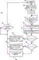
Fig. 5 illustrates a flow chart, and it describes the case method according to the output of the adjustment switching power converter of instruction of the present invention.
Fig. 6 illustrates the interior details according to the example integrated circuit that can realize control technology of instruction of the present invention.
Fig. 7 illustrates the timing waveform according to the example integrated circuit shown in Fig. 6 of instruction of the present invention.
Fig. 8 illustrates a flow chart, and it describes the replacement method example according to instruction of the present invention, in order to adjust the output of switching power converter.
Embodiment
The example that relates to the peak power output of power ratio control converter according to of the present invention is disclosed.In the following description, to understand thoroughly of the present invention in order providing, to have set forth a large amount of specific details.Yet, for a person skilled in the art, it is evident that these specific details not necessarily are used for putting into practice the present invention.In other example, do not describe known material or method in detail for fear of obscuring the present invention.
In whole specification, quoting of " embodiment ", " embodiment ", " example " or " example " meaned that specific feature, structure or the characteristic described in conjunction with the embodiments are included at least one embodiment of the present invention or the example.Therefore, run through this specification and not necessarily mean identical embodiment of generation in different local phrase " in one embodiment ", " in an embodiment ", " in an example " or " in example " that occur.In one or more embodiment or example, described specific feature, structure or characteristic for example can be combined into any suitable combination and/or sub-portfolio.In addition, described specific feature, structure or characteristic can be included in integrated circuit, electronic circuit, combinational logic circuit or can provide in other suitable parts of function described above.In addition, be to be understood that the accompanying drawing that provides in the literary composition all is for the purpose of explaining to those skilled in the art, and accompanying drawing there is no need to draw to scale.
The example of instructing according to the present invention as will be discussed, comprises needn't be at output place sensing output voltage and/or the output current of power inverter for the method and apparatus of the peak power output of power ratio control converter.The tolerance of the protective current limiting threshold value of the example compensation energy transmission inductance tolerance of instructing according to the present invention in addition, and the electric current that in the mains switch of being set by controller, flows.Cancellation has improved power inverter efficient in necessity of the output current of the output place sense power converter of power inverter, has reduced the power inverter number of components, and this has caused comparing with known solution and has improved power inverter reliability.Compensation energy transmission inductance and controller protective current limiting threshold value tolerance have further been improved the power inverter reliability and have been allowed the design of compacter and more reliable power inverter and load.
In an example, during each switching cycle of mains switch, the peak power output of power inverter is controlled to guarantee in the variation of power inverter operating period power inverter in response to energy transmission inductance and protective current limiting threshold value.By the peak power output of power ratio control converter in this way, power inverter is in response to limiting condition for operation (LCO), for example during the initial designs of power inverter, do not expect the very high ambient temperature that occurs also further to have improved the reliability of power inverter and load.
In order to illustrate, Fig. 1 shows an example according to controlled switching power converter 100 of instruction of the present invention, and it is known as power supply sometimes.In the particular instance shown in Fig. 1, switching power converter 100 is the power inverters with flyback topology.Yet be appreciated that according to instruction of the present invention have many other known topological sum structures of Switching Power Supply, it also can control maximum power converter power output, and the flyback topology shown in Fig. 1 is provided is for the purpose of explaining.It should be noted that according to instruction of the present invention in other example, power inverter 100 has more than one output.
Go out as shown, control circuit 115 is coupled to mains switch 105, and it is mos field effect transistor (MOSFET), bipolar transistor etc. in an example.Mains switch 105 is coupled to the input winding 103 of energy transmission 109, and it is coupled to DC input voltage V
IN101 and power output diode 117.In an example, DC input voltage V
INThe 101st, the unadjusted output of being coupled to the rectifier circuit of unshowned AC voltage source.Switching current as the first and second inputs 190 and 191 of flowing through, energy transmission 109 windings 103 and mains switch 105 when input capacitor 106 is coupled to power inverter input 190 and 191 and is in on-state take convenient mains switch 105 provides low impedance source.In an example, control circuit 115 and switch 105 can form the part of integrated circuit, and described integrated circuit can be manufactured to and mix or monolithic integrated circuit.Control circuit 115 is coupled to receive signal 114, it is voltage signal in an example, but it can also be current signal in other example, perhaps can be represent power inverter output and or other signal of input, still benefit from instruction of the present invention simultaneously.
In the example of Fig. 1, control circuit 115 is coupled to adjust from first and second inputs 190 and 191 of power inverter 100 and is delivered to the power inverter output 192 that is coupled in load 121 and 193 power.Energy transmission 109 comprises input winding 103 and output winding 110 and auxiliary winding 108.Signal 114 is coupled to control circuit 115 from auxiliary winding 108 by the resitstance voltage divider (resistordivider) that is made of resistor 111 and 112.As shown in the example, controller 115 comprises current sensing circuit 140, it is coupled with electric current, the sensor circuit 141 of sensing by mains switch 105, it is coupled to receive input signal and timing and the multiplier circuit 142 that represents to the input voltage of power inverter 100, and it processes the output of current sensing circuit 140 and sensor circuit 141.Controller 115 also comprises pierce circuit, it is in response to regularly and multiplier circuit 142 and drive signal generator circuit 144, this drive signal generator circuit be coupled take driving power switch 105 cycle turn-on time as on-state and cycle turn-off time as off state.In an example, the duty ratio that controller 115 is coupled to regulate mains switch 105 makes the product value of itself and input voltage signal and time proportional, the change of electric current between two current values of flowing at mains switch when this time is used for mains switch and is in on-state.
The basic operation of circuit 100 is described referring now to the waveform 200 and 201 among Fig. 2.In operation, in response to the output of signal 114 control circuits 115 by Switching power switch 105 Modulating Power converters 100.When switch 105 is connected, be converted into the inductance of the input winding 103 of described energy transmission 109 from the energy of input capacitor 106.The typical current waveform that in mains switch 105, flows-individual example illustrates with waveform 201 in Fig. 2.When mains switch 105 was connected in the moment 202, the electric current I of the mains switch 105 of flowing through
D203 begin to increase.As shown in the example that illustrates, electric current I after mains switch 105 is switched on
D203 substantial linear increase.Current waveform 204 is along with the rate of change of time is given as:
DI
D/ dt=V
IN/ L
I(1) V wherein
INThe input voltage 101 of crossing over input capacitor 106 among Fig. 1, L
IIt is the inductance L of the input winding 103 of energy transmission 109
I198, it is with in the situation of external circuit coupling not record at all other windings of energy transmission 109.Be noted that the relation in the equation (1) can not illustrate any voltage drop or other second level voltage drop of crossing over mains switch 105 in order not obscure instruction of the present invention.
In the moment 205 that mains switch 105 is turned off, the electric current I that flows in the mains switch 105
D203 value of being increased to I
Dpk206.Be stored in the inductance L of the winding 103 of energy transmission 109
IEnergy in 198 provides by following formula:
When mains switch 105 turn-offs, be stored in the inductance L of input winding 103
IEnergy in 198 is converted into the output of power inverter 100 and flows to capacitor 118 and be coupled to the electric current of the load 121 of output 192 and 193 by forward biased power output diode 117.During the shutoff cycle of switch 105, when electric current is flowed through power output diode 117, cross over the output voltage V of load 121
O119 add that the forward voltage drop of crossing over power output diode 117 is substantially equal to cross over the voltage of output winding 110.
In some cases, during the shutoff cycle of mains switch 105, electric current can be ended basically from output winding 110 flowing by power output diode 117.In this case, the operation of power inverter is called as the discontinuous mode operation.In discontinuous mode operation, before mains switch 105 connects again in beginning, basically be stored in the inductance L of the input winding 103 of energy transmission 109 at next mains switch switching cycle
IAll energy in 198 are transferred to the output of power supply.In the example of Fig. 2, because energy transmits cycle t
Ed207 less than t
Off208, so power inverter operates with discontinuous mode.In the power inverter with discontinuous mode operation, the electric current 203 that flows in the mains switch 105 originates in when each switching cycle begins and is substantially equal to 0 value.If it is T 209 that power inverter 105 switches cycle period, then be delivered to the power (P of the output of power supply
Out) provide by following formula:
P
out=K1×1/2×L
I×I
DPK 2×1/T (3)
Wherein K1 is the factor less than 1, it has illustrated the energy loss from the energy transport that is input to output of power inverter 100, and can for example comprise the loss in the clamp circuit 102 of clamp energy (be commonly called leak energy), described clamp circuit 102 is not in inductance L
I198 and the output coupling of power inverter 100.Item 1/T in the equation (3) is commonly called mains switch switching cycle frequency, and it is decided by controller 115 in an example.
Peak power output ability with the power inverter of discontinuous operation mode can obtain by following formula:
P
outmax=K2×1/2×L
I×I
DPKMAX 2×1/T (4)
I wherein
DPKMAXIt is the maximum protection current limitation current threshold that is determined by controller 115.K2 can be the factor different from K1 in the equation (3), and this is because when comparing with the loading condition of equation (3), the variation of energy loss ratio during the maximum load condition of equation (4).L from a power inverter to another
I, I
DPKMAXTo determine P from a power inverter to another with the tolerance of T
OutmaxTolerance.In addition, in the situation of the operating condition of the ambient temperature of Change Example such as power inverter operation, the L in the single power inverter
I, I
DPKMAXWith the tolerance of T, also will determine P
OutmaxTolerance.
Rearrange now equation (1):
dI
D×L
I=V
IN×dt (5)
The substitution value of maximum power converter loading condition provides:
dI
DPKMAX×L
I=V
IN×dt
onmax (6)
Therefore, according to the relation of equation (6), I
DPKMAXPerhaps L
IAny variation will cause V
IN* dt
OnmaxThe variation of product.As will be described below, in order to generate in response to V
IN* dt
OnmaxThe internal signal of product and the switching cycle period and the V that adjust mains switch 105
IN* dt
OnmaxProduct proportional, controller 115 for example can be coupled to detect and measure V
INAnd dt
ONMAXLike this, mains switch switches cycle period in response to I
DPKMAXPerhaps L
IThereby any variation reduce because I
DPKMAX, L
IThe perhaps variation of the peak power output of the power inverter that causes of the variation of its combination.
I1=K V
IN (7)
Wherein
K={N
AUX/N
I}R
111 (8)
Relational assumption in the top equation (8) terminal 123 when mains switch 105 is positioned at on-state is in the electromotive force of earth terminal 124 basically.
The below describes the example how relation in the equation (6) is used for the peak power output of power ratio control converter with the waveform among Fig. 3.In this example, 300 examples of the waveform among Fig. 3 show two mains switches, 105 current waveforms 303 and 304.In two waveforms 303 and 304, the mains switch electric current I
D302 tilt to and are substantially equal to I
DPKMAX305 end value, it is the protective current limiting threshold value, defines the peak inrush current that can flow in mains switch 105, described mains switch 105 can be set by the controller 115 among Fig. 1 for example.Go out as shown the energy transmission of high X% input winding inductance L in the situation of waveform 304
I, require time that mains switch 105 is in connection to be in the long X% of time of connection than mains switch 105 in the waveform 303, to reach identical protective current limiting threshold value I
DPKMAX305.Therefore directly to input the increase of winding inductance directly proportional with energy transmission in the increase of 105 turn-on times of mains switch, as the relation in the equation (1) is predicted, supposes V
INConstant.If in response to the mains switch increase of 105 turn-on times, the mains switch in the equation (4) switches cycle period T and has also increased X%, so P
OutmaxValue will keep substantially constant because L
IAlso high X%.Therefore, at energy transmission input winding inductance L
IIn the situation of tolerance, be substantially equal to 1 for the corrected value of factor Ka 309.
Yet by the relation in the equation (4), the current limitation threshold value increases the impact of Y% for the peak power output ability P of power inverter 100
OutmaxHas the square-law impact.For example, if the I in the equation (4)
DPKMAXValue has increased by 5%, so the P in the equation (4)
OutmaxValue has increased by 10% basically.Little percentage square for example ± 15% changes and causes substantially doubling the fact that whole percentage changes, and allows the factor Ka 310 among Fig. 3 to be selected as being substantially equal to 2 in order to basically eliminate the impact that mains switch protective current limiting threshold value changes.
Fig. 4 shows signal and the mains switch cycle turn-on time t that mains switch switches the input voltage of cycle period and expression power inverter
OnBetween the curve of relation of product.As discussed above, the value that is substantially equal to 1 Ka will be eliminated energy transmission input winding inductance L basically
IVariation, the value that is substantially equal to simultaneously 2 Ka will be eliminated the variation of the protective current limiting threshold value of controller 115 basically.
Fig. 5 illustrates the flow chart according to the case method of the peak power output that is used for the power ratio control converter of instruction of the present invention.In piece 501, mains switch is connected, and timing cycle begins in piece 502.With reference to what top description was noted be, although the timing cycle of discussing so far is cycle turn-on time of mains switch, but when having the current level of two separation in mains switch, any time during the turn-on time of mains switch, timing cycle can begin and finish.In piece 512, sensing represents to be input to the signal of the input voltage of power inverter.In piece 503, determine because whether timing cycle begins the mains switch electric current and change between two current thresholds.In description up to the present, the first current threshold is substantially equal to 0, the second current threshold and is in the protective current limiting threshold value.Yet be noted that if only need to input to energy transmission the correction of the tolerance of winding inductance, can use so two other current thresholds to determine the slope of mains switch current waveform during mains switch turn-on time.Be noted that at least one in the current threshold in the piece 503 must be the protective current limiting threshold value so if need the tolerance of protective current limiting threshold value to proofread and correct.In piece 504, end regularly, and calculate timer begin and ends between represent the signal of input voltage and the product (KV of Measuring Time
IN* t).Piece 505,506,507,508 and 509 is based on (KV
INThe action that * t) calculative determination needs.Especially, if (KV
IN* t) greater than the rated value in the piece 505 (nominal value), the mains switch switching cycle time increases in piece 507 so.In an example, rated value can just be determined in the Power Management Design stage.Especially, the designer may be calculated the power output rated value that need to obtain and will what be.In order to illustrate, by selecting resistor R
111, and therefore select K, designer can select the nominal operation cycle to be used for the given (V of Fig. 4
IN* t).For example, nominal period can be the point (1,1) among Fig. 4.If (KV
IN* t) greater than this rated value (for example, among Fig. 4 greater than 1), the cycle will increase so.Turn around now with reference to figure 5, if (KV
IN* t) less than the rated value in the piece 506, the mains switch switching will reduce in piece 508 circulation timei so.If (KV
IN* t) be rated value, switch so cycle period in the piece 509 and just can not change.Piece 510 has determined whether current switching cycle period is finished before piece 501 next mains switch switching cycles begin.
Used the conduct of mains switch switching cycle based on (KV although be noted that top description
IN* t) the control parameter adjusted of the measured value of product, but more generally during any mains switch switches cycle period (being called as the mains switch duty ratio), the ratio of mains switch turn-on time and mains switch turn-off time is the wider description of identical control function.Usually; the mains switch duty ratio can be adjusted by adjusting mains switch switching cycle period; and can adjust by other technology, comprise time cycle, ON/OFF control, pulse width modulation or other the suitable power inverter handoff technique adjusting mains switch protective current limiting threshold value, during each switches cycle period, directly control the mains switch connection.
Fig. 6 shows the detailed maps of the some of controller 615, its in an example with Fig. 1 in controller 115 be equivalent.Voltage source V
AUX603 are equivalent to the auxiliary winding voltage V among Fig. 1 in an example
AUX181.In an example, controller 615 is coupled to drive the mains switch of the mains switch 105 that is equivalent among Fig. 1.In an example, resistor 601 is equivalent to the resistor R among Fig. 1
111Ground potential end 605 is equivalent to the ground potential end 124 among Fig. 1 in an example.The below to the description of the circuit 600 among Fig. 6 with reference to the waveform 700 among the figure 7.
As shown in Figure 6, expression is input to the input voltage V of power inverter
IN101 current signal 606 flows during mains switch 105 is connected.Transistor 632 and the coupling of 633 grid keep FB to hold the voltage at 603 places to be substantially equal to controller ground potential 605, thereby the value of current signal 606 is substantially equal to V
AUX/ R
601Current source 634 bias transistors 633.Electric current 606 also flows in transistor 631, and it forms current mirror with transistor 637.Yet because the appearance of transistor 636, it is only in CLK line 607 ability conducting when be high, and the voltage on the grid of transistor 631 is sampled and is maintained on the capacitor 663 until next CLK line signal 607 uprises.Will be noted that, the delay period after mains switch beginning turn-on times 706, CLK line signal waveform 703 uprises.In an example, this delay period was substantially equal to for 400 nanoseconds, and the pulse of CLK line is the high duration to be substantially equal to for 100 nanoseconds.The maintenance voltage of crossing over capacitor 663 is provided with the current value that flows in transistor 637 when transistor 639 conducting.It is transistor 639 conductings during the height that the mains switch gating drives signal 608 and 701, and it is equivalent to the signal 122 among Fig. 1 in an example.In 639 conduction periods of transistor, so capacitor 642 is recharged with fixed current, as shown by the waveform 704 among Fig. 7.Because the value of charging current 610 is determined that by the value of above-mentioned current signal 606 slope response of therefore upper up voltage 707 is in the value of current signal 606, it represents the input voltage of power inverter.Be recharged with this speed at power inverter cycle service time inner capacitor 642, thereby the voltage of crossing over capacitor 642 during mains switch end cycle turn-on time represents the product in input voltage signal and mains switch cycle turn-on time.Be noted that by using only be that high signal replaces gating signal 608 in the part in mains switch cycle turn-on time, can select the time cycle except complete cycle turn-on time of mains switch.Another gating signal CLK-GF 609 turn-on transistor 641 within the short period, it was substantially equal to for 100 nanoseconds in an example, allowed capacitor 643 samplings and maintenance to cross over the voltage of capacitor 642.The delayed version of CLK-GF signal 609 be applied to transistor 640 with replacement capacitor 642 to be ready for during the next switching cycle next mains switch turn-on time.Parts 644,645,646,647,648 and 649 provide the high impedance buffer circuit to guarantee that thereby 643 in capacitor is coupled to high impedance and helps prevent capacitor 643 discharges.This high impedance buffering is used for providing the voltage of crossing over resistor 610, and it is substantially equal to cross over the voltage of capacitor 643.Owing to set up known voltage at known resistance device 610 two ends, thus current known 618 to flow in transistor 651 and be mirrored be the electric current 616 that flows in transistor 652.Be applied to the reference voltage level V of the base stage of transistor 657
Bg+ V
Be612 cross over resistor 611 applies voltage V
Bg, resistor 611 is substantially equal to resistor 610 in an example, sets up electric current 619, and it once and is again reflected to provide electric current 613 by transistor 655 and 654 by transistor 656 reflections.Be noted that diode 653 by reverse bias, and therefore electric current 617 is substantially equal to 0, until above-described electric current 616 surpasses the value of electric current 613.For the value of the electric current 616 that surpasses electric current 613, the electric current 677 that flows is given in electric current 617 contributions in resistor 661, and it adjusts again oscillator voltage level and oscillator frequency, and described oscillator frequency is the inverse that mains switch switches cycle period.In an example, oscillator 604 is included in the capacitor that is recharged and discharges between two node voltages of resistor 661.
What note is that the action of electric current 613 and diode 653 guarantees that electric current 616 can not affect mains switch and switch cycle period below threshold value.This has limited the tolerance that the energy transmission that can be compensated is inputted winding inductance and controller protective current limiting threshold value.
By above-described circuit, be clear that because electric current 677 is the function of the value of resistor 661 for the influence degree of oscillator switching frequency, so the Ka value among Fig. 4 is fixed basically.Therefore be necessary whether selection control is basically fully proofreaied and correct and only partly proofreaied and correct for the tolerance of protective current limiting threshold value thus for the energy transmission inductance.Alternative, can carry out the selection of resistor 661 in order to basically proofread and correct for the protective current limiting threshold value fully and therefore for energy transmission inductance tolerance compensating.In side circuit, the compromise in somewhere between the Ka=1 that can select to provide shown in Figure 4 and the value of Ka=2.An example of the actual selection of Ka value is substantially equal to 1.3.
With reference to the circuit among the figure 1, circuit among Fig. 6 comprises sensor circuit 699, it is equivalent to sensor circuit 141, timing and multiplier circuit 698 in an example, it is equivalent to regularly and multiplier circuit 142 and oscillator 604 in an example, and it is equivalent to pierce circuit 143 in an example.Circuit among Fig. 6 also shows signal 691, and it is equivalent to the signal 146 among Fig. 1 in an example, and it is coupled to and drives signal generating circuit 144; And signal 608, it is equivalent to the output signal 145 from the current sensing circuit 140 among Fig. 1 in an example.
In the particular instance in Fig. 6, because the formation controller gating drives signal 608 when reaching a protective current limiting threshold value, so the gating of mains switch 105 drives the output signal 145 that is equivalent among Fig. 1.Yet be noted that this signal 145 will not correspond to the mains switch gating and drives signal 608 so if the current threshold except the protective current limiting threshold value is used for controlling regularly and multiplier circuit 142 with signal 145.
Above description therefore set forth the detailed realization of circuit execution mode, the part that it can the formation control device, this controller is coupled to mains switch and is coupled to receive expression to the input voltage signal of the input voltage of power supply.To be in the time cycle of on-state be that the electric current that flows in mains switch changes the used time between two current values to mains switch in an example in an example, and the switching cycle period of controller adjustment mains switch is with proportional with the product of input voltage signal and time cycle.
In the above description of control circuit 615, oscillator 604 periodic responses are in the voltage of crossing over resistor 661.Yet should be noted that in another example cycle oscillator is the value of responding digital counter circuit alternately, still benefit from instruction of the present invention simultaneously.In an example, the digit counter circuit increases when being higher than the frequency of mains switch switching frequency, in response to the value of expression to the input signal of the input voltage of power inverter.The value of digit counter counting compares to set oscillator 604 frequencies in the switching cycle of back with number of threshold values subsequently.Note be also can use other technology as recited above for the substituting of control generator cycle, still benefit from widely instruction of the present invention simultaneously.
What note is that the circuit of describing among Fig. 6 is realized adjusting the cycle that provides by the cycle of cycle oscillator.Be noted that and use above-mentioned substituting that wherein cycle oscillator was adjusted in a plurality of cycles, still benefited from the instruction of more wide region of the present invention simultaneously.
Each technology has been described in the description of front, and mains switch switches cycle period and changes the product of used time in response to the signal of statement input voltage and electric current mobile in mains switch between two threshold values and be adjusted thus.Yet be noted that the equivalent method that obtains identity function can be measure time that the electric current that flows in mains switch changes between two threshold values and should the time with expection or the cycle in control time compare, this expection or the control time periodic response arrive the input voltage signal of the input voltage of power supply in expression.Subsequently in response to measure and the cycle in control time between the poor mains switch duty ratio of adjusting.In an example, be to adjust mains switch to switch cycle period for the method for adjusting the mains switch duty ratio.The flow process of Fig. 8 shows a kind of like this method.Mains switch is switched in piece 801, and the signal of expression power input voltage is sensed in piece 802.Timer starts in piece 812, and whether the electric current in the mains switch changes really to fix in the piece 803 between two threshold values and carry out.In piece 804, regularly ended, and calculated t
MeasuredIn piece 811, expection or the cycle in control time, t
ControlCalculated.In piece 805,806,807,808 and 809, mains switch switches cycle period in response to t
ControlAnd t
MeasuredBetween comparison and be adjusted.Especially, if in piece 805 t
Measured>t
Control, mains switch switches cycle period so increases in piece 807.If t in piece 806
Measured<t
Control, mains switch switching cycle period reduces in piece 808 so.If t
MeasuredBe substantially equal to t
Control, mains switch switching cycle period remains unchanged in piece 809 so.
The above description of example illustrated of the present invention comprises the description in the summary, does not attempt exhaustive or limits the present invention in the disclosed accurate form.Of the present invention specific embodiment and the example here described simultaneously all are for schematic purpose, can carry out possible equivalent modifications to it in the situation that does not depart from wider spirit and scope of the present invention.In fact, according to instruction of the present invention, be to be understood that specific voltage, electric current, frequency,, power range values, time etc. all provides for task of explanation and other value also can be used for other embodiment and example.
Can carry out these modifications to example of the present invention according to top detailed description.The term that uses in the following claim it be not desired to limit the invention in specification and the disclosed specific embodiment of claim.On the contrary, scope should be limited by following claim fully, and it is limited to according to claim explains in the scope of setting up.Therefore this specification and accompanying drawing are considered to schematic rather than restrictive.
Claims (25)
1. controller that is used for power inverter comprises:
Input voltage sensor, it is coupled to receive the input signal of the input voltage that represents power inverter;
Current sensor, it is coupled the electric current that flows with sensing in mains switch; And
Drive signal generator, its be coupled take the driving power switch cycle turn-on time as on-state and cycle turn-off time as off state, wherein this drive signal generator switching cycle period of being coupled to adjust mains switch makes the product of described switching cycle period and following two values proportional:
1) input signal;
2) electric current that flows in mains switch when mains switch is in on-state changes the used time between the first current value and the second current value.
2. according to claim 1 the controller that is used for power inverter, one in wherein said the first current value and the second current value is essentially 0.
3. according to claim 1 the controller that is used for power inverter, one in wherein said the first current value and the second current value is the protective current limiting value.
4. according to claim 1 the controller that is used for power inverter, wherein this input signal is voltage.
5. according to claim 1 the controller that is used for power inverter, wherein this input signal is the current signal of the input voltage of expression power inverter.
6. according to claim 1 the controller that is used for power inverter, wherein the switching cycle period of this mains switch is in response to the variation of the inductance of the energy transmission of power inverter.
7. according to claim 1 the controller that is used for power inverter further comprises pierce circuit, and it is coupled to provide a signal to this drive signal generator.
8. according to claim 7 the controller that is used for power inverter, further comprise timing and multiplier circuit, it is coupled to process the output of this current sensor and the output of input voltage sensor, and wherein this pierce circuit is coupled with in response to this timing and multiplier circuit.
9. controller that is used for power inverter comprises:
Input voltage sensor, it is coupled to receive the input signal of the input voltage that represents this power inverter;
Current sensor, it is coupled the electric current that flows with sensing in mains switch; And
Drive signal generator, its be coupled take the driving power switch cycle turn-on time as on-state and cycle turn-off time as off state, wherein this drive signal generator duty ratio of being coupled to adjust this mains switch makes the product of described duty ratio and following two values proportional:
1) input signal;
2) electric current that flows in mains switch when mains switch is in on-state changes the used time between the first current value and the second current value.
10. according to claim 9 the controller that is used for power inverter, one in wherein said the first current value and the second current value is essentially 0.
11. the controller that is used for power inverter according to claim 9, one in wherein said the first current value and the second current value is the protective current limiting value.
12. the controller that is used for power inverter according to claim 9 further comprises pierce circuit, it is coupled to provide signal to this drive signal generator.
13. the controller that is used for power inverter according to claim 12, further comprise timing and multiplier circuit, it is coupled to process the output of current sensor and the output of input voltage sensor, and wherein this pierce circuit is coupled with in response to this timing and multiplier circuit.
14. a controller that is used for power inverter comprises:
Input voltage sensor, it is coupled to receive the input signal of the input voltage that represents this power inverter;
Current sensor, it is coupled the electric current that flows with sensing in mains switch; And
Drive signal generator, its be coupled take the driving power switch cycle turn-on time as on-state and cycle turn-off time as off state, wherein this drive signal generator is coupled to adjust the switching cycle period of this mains switch in response to following value: this value is the electric current that flows in mains switch when mains switch is in on-state and cycle in control time the poor of used time that change between the first current value and the second current value.
15. the controller that is used for power inverter according to claim 14, one in wherein said the first current value and the second current value is essentially 0.
16. the controller that is used for power inverter according to claim 14, one in wherein said the first current value and the second current value is the protective current limiting value.
17. the controller that is used for power inverter according to claim 14, if the electric current that wherein flows in mains switch when mains switch is in on-state changes the used time greater than the described cycle in control time between the first current value and the second current value, this controller is coupled to increase the switching cycle period of this mains switch so.
18. the controller that is used for power inverter according to claim 14, if the electric current that wherein flows in mains switch when mains switch is in on-state changes the used time less than the cycle in control time between the first current value and the second current value, this controller is coupled to reduce the switching cycle period of this mains switch so.
19. the controller that is used for power inverter according to claim 14 further comprises pierce circuit, it is coupled to produce the signal that is coupled with driven signal generator reception.
20. the controller that is used for power inverter according to claim 19, further comprise timing and multiplier circuit, it is coupled to process the output of this current sensor and the output of input voltage sensor, and wherein this pierce circuit is coupled with in response to this timing and multiplier circuit.
21. a method that is used for the power ratio control converter comprises:
Turning on and off Switching power switch between the state;
Sensing represents the input signal of the input voltage of power inverter;
The electric current that sensing flows in mains switch; And
The switching cycle period of adjusting mains switch makes the product of described switching cycle period and following two values proportional:
1) input signal;
2) electric current that flows in mains switch when mains switch is in on-state changes the used time between the first current value and the second current value.
22. the method that is used for the power ratio control converter according to claim 21 comprises that further the electric current of determining to flow is from being essentially for 0 second time that value is used that changes to described the first current value and the second current value in mains switch.
23. the method that is used for the power ratio control converter according to claim 21 further comprises and determine that electric current first value from described the first current value and the second current value that flows changes to the used time of protective current limiting value in mains switch.
24. the method that is used for the power ratio control converter according to claim 21, wherein sensing represents that the input signal of the input voltage of power inverter comprises sensing voltage.
25. the method that is used for the power ratio control converter according to claim 21, wherein sensing represents that the input signal of the input voltage of power inverter is included in current sensor during the cycle that mains switch is in on-state.
Priority Applications (1)
| Application Number | Priority Date | Filing Date | Title |
|---|---|---|---|
| CN201310053532.7A CN103151934B (en) | 2007-04-06 | 2008-04-07 | For controlling the method and apparatus of the peak power output of power inverter |
Applications Claiming Priority (6)
| Application Number | Priority Date | Filing Date | Title |
|---|---|---|---|
| US92219107P | 2007-04-06 | 2007-04-06 | |
| US60/922,191 | 2007-04-06 | ||
| US60/922191 | 2007-04-06 | ||
| US12/058,539 US7746050B2 (en) | 2007-04-06 | 2008-03-28 | Method and apparatus for controlling the maximum output power of a power converter |
| US12/058539 | 2008-03-28 | ||
| US12/058,539 | 2008-03-28 |
Related Child Applications (1)
| Application Number | Title | Priority Date | Filing Date |
|---|---|---|---|
| CN201310053532.7A Division CN103151934B (en) | 2007-04-06 | 2008-04-07 | For controlling the method and apparatus of the peak power output of power inverter |
Publications (2)
| Publication Number | Publication Date |
|---|---|
| CN101286703A CN101286703A (en) | 2008-10-15 |
| CN101286703B true CN101286703B (en) | 2013-03-20 |
Family
ID=39826387
Family Applications (2)
| Application Number | Title | Priority Date | Filing Date |
|---|---|---|---|
| CN201310053532.7A Expired - Fee Related CN103151934B (en) | 2007-04-06 | 2008-04-07 | For controlling the method and apparatus of the peak power output of power inverter |
| CN2008101092202A Expired - Fee Related CN101286703B (en) | 2007-04-06 | 2008-04-07 | Method and apparatus for controlling the maximum output power of a power converter |
Family Applications Before (1)
| Application Number | Title | Priority Date | Filing Date |
|---|---|---|---|
| CN201310053532.7A Expired - Fee Related CN103151934B (en) | 2007-04-06 | 2008-04-07 | For controlling the method and apparatus of the peak power output of power inverter |
Country Status (3)
| Country | Link |
|---|---|
| US (5) | US7746050B2 (en) |
| JP (2) | JP5438282B2 (en) |
| CN (2) | CN103151934B (en) |
Families Citing this family (27)
| Publication number | Priority date | Publication date | Assignee | Title |
|---|---|---|---|---|
| US7296881B2 (en) * | 2005-01-21 | 2007-11-20 | Hewlett-Packard Development Company, L.P. | Printhead de-priming |
| US7746050B2 (en) | 2007-04-06 | 2010-06-29 | Power Integrations, Inc. | Method and apparatus for controlling the maximum output power of a power converter |
| US8576595B2 (en) * | 2008-07-09 | 2013-11-05 | System General Corp. | Method and apparatus of providing a biased current limit for limiting maximum output power of power converters |
| US8045351B2 (en) * | 2008-07-09 | 2011-10-25 | System General Corp. | Method and apparatus of providing a biased current limit for limiting maximum output power of power converters |
| US8432147B2 (en) * | 2008-07-23 | 2013-04-30 | Semiconductor Components Industries, Llc | Method of forming a switching regulator and structure therefor |
| US8098506B2 (en) | 2009-06-02 | 2012-01-17 | Power Integrations, Inc. | Single-stage power supply with power factor correction and constant current output |
| JP2011062026A (en) * | 2009-09-11 | 2011-03-24 | Panasonic Corp | Switching power supply device and semiconductor device |
| US8582267B2 (en) * | 2010-03-05 | 2013-11-12 | The Charles Stark Draper Laboratory, Inc. | System and method to limit in-rush current |
| TWI411202B (en) * | 2010-12-20 | 2013-10-01 | Richtek Technology Corp | Controller for power converter and method for controlling power converter |
| JP5737963B2 (en) * | 2011-01-21 | 2015-06-17 | キヤノン株式会社 | Switching power supply and image forming apparatus having switching power supply |
| US8531853B2 (en) * | 2011-07-28 | 2013-09-10 | Power Integrations, Inc. | Variable frequency timing circuit for a power supply control circuit |
| US8611116B2 (en) * | 2011-07-28 | 2013-12-17 | Power Integrations, Inc. | Varying switching frequency and period of a power supply controller |
| US8717785B2 (en) * | 2011-09-30 | 2014-05-06 | Power Integrations, Inc. | Multi-stage sampling circuit for a power converter controller |
| US8797016B2 (en) * | 2011-11-09 | 2014-08-05 | Saher Waseem | Apparatus and method for power extraction from high impedance sources |
| JP5927877B2 (en) * | 2011-12-06 | 2016-06-01 | 富士電機株式会社 | Switching power supply |
| KR101339621B1 (en) | 2012-11-26 | 2013-12-10 | 삼성전기주식회사 | Dc/dc converter having multi-piuput |
| JP2016525259A (en) * | 2013-07-25 | 2016-08-22 | ボーンズ、インコーポレイテッド | Non-insulated AC-DC power supply |
| US9825541B2 (en) * | 2014-01-17 | 2017-11-21 | Fairchild Korea Semiconductor Ltd. | Output current estimating method and power supply device using the same |
| CN104298288B (en) * | 2014-10-29 | 2016-04-13 | 中国民用航空飞行学院 | Airborne ADS-B electric power management circuit |
| US10250144B2 (en) | 2015-07-08 | 2019-04-02 | Infineon Technologies Austria Ag | Input voltage detection for a power converter including a transformer having a primary side and a secondary side |
| US10361554B1 (en) * | 2016-09-27 | 2019-07-23 | Altera Corporation | Techniques for determining inductances |
| US10243442B1 (en) | 2017-11-22 | 2019-03-26 | Power Integrations, Inc. | Controller with frequency to on-time converter |
| CN110168895B (en) * | 2017-12-12 | 2024-04-05 | 雅达电子国际有限公司 | Resonant converter power supply and method for reducing unbalanced current therein |
| CN113056866A (en) | 2018-11-28 | 2021-06-29 | 斯兰纳亚洲有限公司 | Digitally compensated current sensing protection |
| CN111781436B (en) * | 2019-04-04 | 2021-07-13 | 株洲中车时代电气股份有限公司 | Fault detection device and method for current converter and current conversion system |
| US10944330B1 (en) * | 2019-12-19 | 2021-03-09 | Cypress Semiconductor Corporation | Self-biased gate driver architecture |
| US11942900B2 (en) | 2021-10-14 | 2024-03-26 | Power Integrations, Inc. | Signal compensation with summed error signals |
Citations (4)
| Publication number | Priority date | Publication date | Assignee | Title |
|---|---|---|---|---|
| CN1114520A (en) * | 1993-08-11 | 1996-01-03 | Ntt移动通信网株式会社 | Apparatus for automatically controlling gain, communication apparatus, and method for automatically controlling gain |
| US5828558A (en) * | 1998-02-11 | 1998-10-27 | Powerdsine, Ltd. | PWN controller use with open loop flyback type DC to AC converter |
| US6057665A (en) * | 1998-09-18 | 2000-05-02 | Fire Wind & Rain Technologies Llc | Battery charger with maximum power tracking |
| WO2005109615A2 (en) * | 2004-05-11 | 2005-11-17 | Thales | Anharmonic low-current ac-dc converter |
Family Cites Families (18)
| Publication number | Priority date | Publication date | Assignee | Title |
|---|---|---|---|---|
| US5220492A (en) * | 1989-12-26 | 1993-06-15 | Systel Development And Industries Ltd. | Inverter and power supply systems including same |
| JP2831517B2 (en) * | 1992-10-21 | 1998-12-02 | 日本電信電話株式会社 | DC power supply system for fuel cells |
| FR2729516B1 (en) * | 1995-01-13 | 1997-04-18 | Sextant Avionique | BIDIRECTIONAL CONTINUOUS-CONTINUOUS VOLTAGE CONVERTERS AND CURRENT SENSOR |
| US6233161B1 (en) | 2000-03-02 | 2001-05-15 | Power Integrations, Inc. | Switched mode power supply responsive to voltage across energy transfer element |
| US6480399B2 (en) | 2000-03-02 | 2002-11-12 | Power Integrations, Inc. | Switched mode power supply responsive to current derived from voltage across energy transfer element input |
| US6862198B2 (en) | 2001-11-29 | 2005-03-01 | Iwatt, Inc. | PWM power converter with digital sampling control circuitry |
| US6833692B2 (en) * | 2002-01-17 | 2004-12-21 | Power Integrations, Inc. | Method and apparatus for maintaining an approximate constant current output characteristic in a switched mode power supply |
| US7288924B2 (en) * | 2004-07-16 | 2007-10-30 | Cellex Power Products, Inc. | Digital input current control for switch mode power supplies |
| US7259972B2 (en) * | 2004-10-07 | 2007-08-21 | System General Corporation | Primary-side-control power converter having a switching controller using frequency hopping and voltage and current control loops |
| US7019503B1 (en) * | 2005-02-07 | 2006-03-28 | Raytheon Company | Active power filter with input voltage feedforward, output load feedforward, and output voltage feedforward |
| US7352595B2 (en) * | 2005-11-08 | 2008-04-01 | System General Corp. | Primary-side controlled switching regulator |
| US7505287B1 (en) * | 2005-11-10 | 2009-03-17 | Iwatt Inc. | On-time control for constant current mode in a flyback power supply |
| US7414865B2 (en) * | 2005-11-17 | 2008-08-19 | System General Corp. | Controller having output current control for a power converter |
| CN100461599C (en) * | 2005-12-05 | 2009-02-11 | 崇贸科技股份有限公司 | Power converter controller |
| JP4704918B2 (en) * | 2006-01-12 | 2011-06-22 | セイコーインスツル株式会社 | Switching regulator |
| US7463497B2 (en) * | 2006-08-07 | 2008-12-09 | Linear Technology Corporation | Regulator for isolated flyback power supply using primary side sensing |
| US7639517B2 (en) * | 2007-02-08 | 2009-12-29 | Linear Technology Corporation | Adaptive output current control for switching circuits |
| US7746050B2 (en) | 2007-04-06 | 2010-06-29 | Power Integrations, Inc. | Method and apparatus for controlling the maximum output power of a power converter |
-
2008
- 2008-03-28 US US12/058,539 patent/US7746050B2/en not_active Expired - Fee Related
- 2008-04-07 CN CN201310053532.7A patent/CN103151934B/en not_active Expired - Fee Related
- 2008-04-07 JP JP2008099744A patent/JP5438282B2/en not_active Expired - Fee Related
- 2008-04-07 CN CN2008101092202A patent/CN101286703B/en not_active Expired - Fee Related
-
2010
- 2010-05-14 US US12/780,658 patent/US8030912B2/en not_active Expired - Fee Related
-
2011
- 2011-09-16 US US13/235,284 patent/US8502517B2/en not_active Expired - Fee Related
-
2013
- 2013-07-05 US US13/935,897 patent/US8872500B2/en not_active Expired - Fee Related
- 2013-12-12 JP JP2013256781A patent/JP5694494B2/en not_active Expired - Fee Related
-
2014
- 2014-09-25 US US14/496,967 patent/US20150009720A1/en not_active Abandoned
Patent Citations (4)
| Publication number | Priority date | Publication date | Assignee | Title |
|---|---|---|---|---|
| CN1114520A (en) * | 1993-08-11 | 1996-01-03 | Ntt移动通信网株式会社 | Apparatus for automatically controlling gain, communication apparatus, and method for automatically controlling gain |
| US5828558A (en) * | 1998-02-11 | 1998-10-27 | Powerdsine, Ltd. | PWN controller use with open loop flyback type DC to AC converter |
| US6057665A (en) * | 1998-09-18 | 2000-05-02 | Fire Wind & Rain Technologies Llc | Battery charger with maximum power tracking |
| WO2005109615A2 (en) * | 2004-05-11 | 2005-11-17 | Thales | Anharmonic low-current ac-dc converter |
Also Published As
| Publication number | Publication date |
|---|---|
| US8502517B2 (en) | 2013-08-06 |
| US20130294117A1 (en) | 2013-11-07 |
| JP5694494B2 (en) | 2015-04-01 |
| US20120007575A1 (en) | 2012-01-12 |
| US20100220503A1 (en) | 2010-09-02 |
| US8030912B2 (en) | 2011-10-04 |
| US7746050B2 (en) | 2010-06-29 |
| JP2014045653A (en) | 2014-03-13 |
| US8872500B2 (en) | 2014-10-28 |
| US20150009720A1 (en) | 2015-01-08 |
| JP5438282B2 (en) | 2014-03-12 |
| CN101286703A (en) | 2008-10-15 |
| US20080246456A1 (en) | 2008-10-09 |
| CN103151934A (en) | 2013-06-12 |
| JP2008259418A (en) | 2008-10-23 |
| CN103151934B (en) | 2015-09-16 |
Similar Documents
| Publication | Publication Date | Title |
|---|---|---|
| CN101286703B (en) | Method and apparatus for controlling the maximum output power of a power converter | |
| US10848069B2 (en) | Systems and methods of operation for power converters having series-parallel mode active clamps | |
| US8143875B2 (en) | Method and apparatus to limit output power in a switching power supply | |
| US8013584B2 (en) | Method and apparatus for maintaining a constant load current with line voltage in a switch mode power supply | |
| US7710095B2 (en) | Power converter having PWM controller for maximum output power compensation | |
| US8964412B2 (en) | Split current mirror line sensing | |
| US8767423B2 (en) | Method and apparatus for varying current limit to limit an output power of a power supply | |
| EP1990903A2 (en) | Method and apparatus for controlling the maximum output power of a power converter | |
| CN101330256B (en) | Method and apparatus for regulating a diode conduction duty cycle |
Legal Events
| Date | Code | Title | Description |
|---|---|---|---|
| C06 | Publication | ||
| PB01 | Publication | ||
| C10 | Entry into substantive examination | ||
| SE01 | Entry into force of request for substantive examination | ||
| C14 | Grant of patent or utility model | ||
| GR01 | Patent grant | ||
| CF01 | Termination of patent right due to non-payment of annual fee |
Granted publication date: 20130320 Termination date: 20210407 |
|
| CF01 | Termination of patent right due to non-payment of annual fee |