CN101276084A - Display device - Google Patents
Display device Download PDFInfo
- Publication number
- CN101276084A CN101276084A CNA2008100963564A CN200810096356A CN101276084A CN 101276084 A CN101276084 A CN 101276084A CN A2008100963564 A CNA2008100963564 A CN A2008100963564A CN 200810096356 A CN200810096356 A CN 200810096356A CN 101276084 A CN101276084 A CN 101276084A
- Authority
- CN
- China
- Prior art keywords
- display panel
- thin
- light
- display device
- film component
- Prior art date
- Legal status (The legal status is an assumption and is not a legal conclusion. Google has not performed a legal analysis and makes no representation as to the accuracy of the status listed.)
- Pending
Links
Images


Classifications
-
- G—PHYSICS
- G02—OPTICS
- G02F—OPTICAL DEVICES OR ARRANGEMENTS FOR THE CONTROL OF LIGHT BY MODIFICATION OF THE OPTICAL PROPERTIES OF THE MEDIA OF THE ELEMENTS INVOLVED THEREIN; NON-LINEAR OPTICS; FREQUENCY-CHANGING OF LIGHT; OPTICAL LOGIC ELEMENTS; OPTICAL ANALOGUE/DIGITAL CONVERTERS
- G02F1/00—Devices or arrangements for the control of the intensity, colour, phase, polarisation or direction of light arriving from an independent light source, e.g. switching, gating or modulating; Non-linear optics
- G02F1/01—Devices or arrangements for the control of the intensity, colour, phase, polarisation or direction of light arriving from an independent light source, e.g. switching, gating or modulating; Non-linear optics for the control of the intensity, phase, polarisation or colour
- G02F1/13—Devices or arrangements for the control of the intensity, colour, phase, polarisation or direction of light arriving from an independent light source, e.g. switching, gating or modulating; Non-linear optics for the control of the intensity, phase, polarisation or colour based on liquid crystals, e.g. single liquid crystal display cells
- G02F1/133—Constructional arrangements; Operation of liquid crystal cells; Circuit arrangements
- G02F1/1333—Constructional arrangements; Manufacturing methods
- G02F1/1335—Structural association of cells with optical devices, e.g. polarisers or reflectors
- G02F1/133509—Filters, e.g. light shielding masks
- G02F1/133512—Light shielding layers, e.g. black matrix
-
- G—PHYSICS
- G02—OPTICS
- G02F—OPTICAL DEVICES OR ARRANGEMENTS FOR THE CONTROL OF LIGHT BY MODIFICATION OF THE OPTICAL PROPERTIES OF THE MEDIA OF THE ELEMENTS INVOLVED THEREIN; NON-LINEAR OPTICS; FREQUENCY-CHANGING OF LIGHT; OPTICAL LOGIC ELEMENTS; OPTICAL ANALOGUE/DIGITAL CONVERTERS
- G02F1/00—Devices or arrangements for the control of the intensity, colour, phase, polarisation or direction of light arriving from an independent light source, e.g. switching, gating or modulating; Non-linear optics
- G02F1/01—Devices or arrangements for the control of the intensity, colour, phase, polarisation or direction of light arriving from an independent light source, e.g. switching, gating or modulating; Non-linear optics for the control of the intensity, phase, polarisation or colour
- G02F1/13—Devices or arrangements for the control of the intensity, colour, phase, polarisation or direction of light arriving from an independent light source, e.g. switching, gating or modulating; Non-linear optics for the control of the intensity, phase, polarisation or colour based on liquid crystals, e.g. single liquid crystal display cells
- G02F1/133—Constructional arrangements; Operation of liquid crystal cells; Circuit arrangements
- G02F1/1333—Constructional arrangements; Manufacturing methods
- G02F1/133342—Constructional arrangements; Manufacturing methods for double-sided displays
Landscapes
- Physics & Mathematics (AREA)
- Nonlinear Science (AREA)
- Mathematical Physics (AREA)
- Chemical & Material Sciences (AREA)
- Crystallography & Structural Chemistry (AREA)
- General Physics & Mathematics (AREA)
- Optics & Photonics (AREA)
- Liquid Crystal (AREA)
- Devices For Indicating Variable Information By Combining Individual Elements (AREA)
Abstract
A display device includes a light-providing part, a first display panel part disposed at a first side of the light-providing part, a second display panel part disposed at a second side of the light-providing part, a receiving part disposed between the second display panel part and the light-providing part and a film member disposed between the second display panel part and the receiving part. The film member has an opening formed corresponding to the second display panel part. The film member reduces the amount of reflected light that is directed to the first side of the light-providing part. Thus, the display device has a simplified structure and improved display quality.
Description
Technical field
The present invention relates to a kind of display device.In more detail, the present invention relates to have the display device of two displays.
Background technology
LCD (LCD) as the panel display apparatus type utilizes the electricity of liquid crystal and light characteristic to come display image.
At present, have the LCD device of two displays, for example, be used in the undersized LCD device.Described LCD device comprises a main LCD panel and size secondary LCD panel less than main LCD panel.
In having traditional LCD device of two displays, be provided with and the corresponding casing of secondary LCD panel.For example, this secondary LCD panel is corresponding to running through the opening setting that casing forms.Here, be shown on the main LCD panel, therefore, worsen the display quality of LCD device with the shape of secondary LCD panel corresponding opening.
Summary of the invention
Embodiments of the invention provide a kind of display device, and it can improve the display quality of display panel.
Display device comprises for light part, the first display panel part, second display panel part, holding portion and the thin-film component according to an embodiment of the invention.The described light part that supplies provides light to first example with second side relative with first side.First side that described first display panel partly is arranged on for the light part shows first image to utilize the light that points to first side that supplies the light part.Second side that described second display panel partly is arranged on for the light part shows second image to utilize the light that points to second side that supplies the light part.Described second image is less than described first image.The described accommodation section branch is arranged on described second display panel part and described for described for light part and the described first display panel part to hold between the light part.Described thin-film component is arranged between described second display panel part and the described accommodation section branch, to reduce the reflection light quantity that points to for first side of light part.Described reflected light is the light that is reflected then on second side of initial directional for the light part.Described thin-film component has and forms and the corresponding opening of the second display panel part.
In an exemplary embodiment, described thin-film component have form be adjacent to described opening and with the corresponding engaging zones of peripheral part of described second display panel part.The engaging zones of described thin-film component can be joined to the peripheral part of described second display panel part by attaching components.Described display device can further comprise and forms the alignment member that is adjacent to described engaging zones to guide at least one side of described second display panel part.
For example, described second display panel part can comprise the display panel that shows second image and be configured to hold the framed of described display panel.The engaging zones of thin-film component can join the framed peripheral part that holds display panel to.
Described thin-film component can be colored, to reduce the reflection light quantity that points to for light part first side.Described thin-film component can comprise black and grey.
Described thin-film component and described accommodation section are divided and can be bonded with each other by bonding part.
In an exemplary embodiment, described display device can comprise further that the optical element that is arranged between described accommodation section branch and the described thin-film component is to improve the optical property of pointing to for the light of light parts second side.Described optical element can have the corresponding engaging zones of peripheral part with second display panel part.For example, the engaging zones of described optical element can join the peripheral part of second display panel part by bonding part to.
Display device according to the embodiment of the invention comprises backlight assembly, first display panel, second display panel, the first framed and thin-film component.Backlight assembly supplies light to first example and second side relative with first side.First display panel is arranged on first side of backlight assembly so that utilize the light that points to backlight assembly first side to show first image.Second display panel is arranged on second side of backlight assembly so that utilize the light that points to backlight assembly second side to show second image.Described second image is less than described first image.Described first framed being arranged between described second display panel and the backlight assembly to hold described backlight assembly and described first display panel.Described thin-film component be arranged on described second display panel and described first framed between reduce to point to the reflection light quantity of described backlight assembly first side.Described reflected light is the light that initial directional backlight assembly second side is reflected then.Described thin-film component has and forms and the corresponding opening of second display panel.
In an exemplary embodiment, described thin-film component can have with the corresponding engaging zones of the peripheral part of second display panel to join the peripheral part of second display panel to.
In an exemplary embodiment, described display device can further comprise and is configured to hold the second framed of second display panel.Described thin-film component can have with the second framed corresponding engaging zones of circumferential component to join the second framed peripheral part to.
According to embodiments of the invention, thin-film component has reduced the reflection light quantity that points to on light parts first side.Therefore, the display quality of display device can improve, and can save casing to simplify the structure of display device.
Description of drawings
By the description of following description taken in conjunction accompanying drawing, can understand exemplary embodiment of the present invention in further detail, wherein:
Fig. 1 has illustrated the decomposition diagram of display device according to an exemplary embodiment of the present invention;
Fig. 2 is the sectional view along the I-I ' line among Fig. 1;
Fig. 3 has illustrated the sectional view of the joint of second display panel of the display device shown in Fig. 1 and thin-film component;
Fig. 4 has illustrated the thin-film component of the display device shown in Fig. 1 and the framed skeleton view that engages;
Fig. 5 has illustrated according to second display panel of the display device of exemplary embodiment of the present invention and the skeleton view that engages of thin-film component;
Fig. 6 has illustrated according to second display panel of the display device of exemplary embodiment of the present invention and the skeleton view that engages of thin-film component; And
Fig. 7 has illustrated according to second display panel of the display device of exemplary embodiment of the present invention and the skeleton view that engages of optical element;
Embodiment
Next, exemplary embodiment of the present invention will be described in conjunction with the accompanying drawings more all sidedly.Yet the form that the present invention is can be multiple different is implemented and the embodiment that should not be considered as being confined to here and set forth.In the accompanying drawings, be clear finding, the size in layer and zone and relative size may be by exaggerative.Be understandable that, when an element or layer be called as another one element or layer " on ", " being connected to " or " joining to " to another one element or when layer, it can be directly thereon, is directly connected to or joins to described another one element or layer, perhaps can have intermediary element or layer.Fig. 1 is the decomposition diagram that has illustrated according to the display device of exemplary embodiment of the present invention.Fig. 2 is the sectional view along the I-I ' line among Fig. 1.
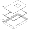
With reference to figure 1 and Fig. 2, display device 1000 comprises for light part 100, the first display panel part 200, the second display panel parts 300, holding portion 400 and thin-film components 500.
The described light part 100 that supplies provides light to first side with second side relative with first side, and comprises light source 110 and photocon 120.
The light that described photocon 120 levels guiding is produced by described light source 110.Leave photocon 120 directives first side by first light-emitting face, 122, the first light.Penetrate by second light-emitting face, 124, the second light and to leave photocon 120 directives second side.
The described first display panel part 200 is arranged on first side for light part 100, and utilizes first light that points to first side to show first image.
The described second display panel part 300 is arranged on second side for light part 100, and utilizes second light that points to second side to show second image.Described second image is less than described first image.
The described first display panel part 200 comprises first display panel 210, and the described second display panel part 300 comprises second display panel 310.
Described first display panel 210 comprises first substrate 212 and second substrate 214, and described second display panel 310 comprises first substrate 312 and second substrate 314.In one exemplary embodiment, first substrate 212 and 312 can be corresponding to the thin film transistor (TFT) with TFT (TFT) substrate, and second substrate 214 and 314 can be corresponding to the filter substrate with color filter.The liquid crystal layer (not shown) is respectively placed between first substrate 212 and 312 and second substrate 214 and 314.
The described accommodation section divides 400 to be arranged between described second display panel part 300 and the confession light part 100, and holds for the light part 100 and the first display panel part 200.The described accommodation section divides 400 also to hold thin-film component 500, will be described in detail it below.As shown in fig. 1, the described accommodation section divides 400 to be have frame shape framed.
Described thin-film component 500 form with the second display panel part, 300 corresponding opening OP in hold the described second display panel part 300.Described thin-film component 500 is arranged on the described accommodation section and divides in 400.
By for the part of second light of second side that light part 100 produces and points to by opening OP and arrive the second display panel part 310.Another part in second light arrives thin-film component 500.
The most of light that arrives the second display panel part 310 is used to display image on the second display panel part 310, and sub-fraction light is to first lateral reflection.Except described opening OP, the light portion that arrives thin-film component 500 is absorbed by thin-film component 500, and part is from thin-film component 500 reflections.
Described thin-film component 500 has reduced the reflection light quantity that points to for first side of light part 100.Described reflected light is an initial directional for second side of light part 100 and then from the light of described thin- film component 500 and 310 reflections of the described second display panel part.The result, very little from the light quantity of described thin-film component 500 reflections and difference between the light quantity that reflects from the described second display panel part 310, the image that is shown in like this on the first display panel part 210 has uniform brightness, thereby the shape that has prevented opening OP is shown on the first display panel part 210.Therefore, the display quality of display device 1000 is improved.
Thin-film component 500 can comprise, for example polyethylene terephthalate (PET).
Because described display device 1000 utilizes described thin-film component 500 to limit the structure of display device 1000, thus casing included in the conventional display device can be saved, thus simplified the structure of display device 1000.
Described thin-film component 500 can be colored to reduce and point to described reflection light quantity for light part 100 first sides.The optical reflectivity that arrives the light of thin-film component 500 can change according to the color difference.Thereby described thin-film component 500 can be dark to reduce the described reflection light quantity for light part 100 first sides of sensing.For example, described thin-film component 500 can comprise black or grey.
Described display device 1000 optionally comprises first optical element 600 and/or second optical element 700.
Described first and second optical elements 600 and 700 improve first side and first light of second side and the optical characteristics of pointing to for light part 100 of second light respectively.For example, each the comprised light diffusion sheet in first and second optical elements 600 and 700, prismatic lens, dual brightness enhancement film (DBEF) etc.
Described light diffusion sheet improves brightness equably, and described prismatic lens improves the visual angle, and described DBEF improves brightness and visual angle.
In Fig. 1 and Fig. 2, described first optical element 600 is arranged on the described accommodation section and divides under 400.Perhaps, described first optical element 600 can be arranged on the described accommodation section and divides on 400.
Described thin-film component 500 comprises opening OP, and have with the corresponding engaging zones CA of the peripheral part of the described second display panel part 300 to join the peripheral part of the described second display panel part 300 to.Therefore, at engaging zones CA, the described second display panel part 300 can join described thin-film component 500 to.
Below, with engaging of the more detailed description second display panel part 300 in conjunction with the accompanying drawings and thin-film component 500.
Fig. 3 is the sectional view that engages that second display panel part and thin-film component in the display device shown in Fig. 1 have been described.
With reference to figure 3, the described second display panel part 300 comprises that described second display panel 310 and framed 320, described framed 320 holds described second display panel 310.
As shown in Figure 3, the described framed 320 engaging zones CA that are engaged to thin-film component 500.For example, framed 320 peripheral part is corresponding to engaging zones CA, and described engaging zones CA joins framed 320 peripheral part to.In addition, by attaching components 10, the engaging zones CA of described thin-film component 500 is engaged to described framed 320 peripheral part.Described attaching components 10 for example can comprise double sticky tape.
The effective viewing area that comprises the not overlapping described second display panel part 310 of described thin-film component 500 of engaging zones CA.Therefore, the effective viewing area on the second display panel part 310 can not reduced by described thin-film component 500 basically.
In Fig. 1 to 3, described engaging zones CA forms and is adjacent to the opening OP that for example has quadrangle form, and corresponding to the four edges of described quadrangle form.Perhaps, engaging zones CA can form and be adjacent to opening OP, and corresponding to one side, both sides or three limits of described quadrangle form.
Fig. 4 has illustrated the thin-film component of the display device shown in Fig. 1 and the framed skeleton view that engages.
With reference to figure 4, the described accommodation section divides 400 to comprise that step part 410 is to hold and to support described thin-film component 500.
Described thin-film component 500 can divide 400 to be bonded with each other by attaching components 20 and described accommodation section.For example, the peripheral part of described thin-film component 500 joins the described accommodation section to by described attaching components 20 and divides 400 step part 410.Therefore, can prevent that described thin-film component 500 breaks away from described accommodation sections and divides 400 and move freely.
Described attaching components 20 for example, can comprise double sticky tape.
Fig. 5 has illustrated according to second display panel of the display device of exemplary embodiment of the present invention and the skeleton view that engages of thin-film component.With reference to figure 5, described display device comprises the alignment member 510 that is formed on the thin-film component 500.
Described alignment member 510 forms and is adjacent to described engaging zones CA, to guide at least one side of the described second display panel part 300.Therefore, compare with the situation of not using alignment member, described alignment member 510 can be registered to the second display panel part 300 accurate more position.In an exemplary embodiment, two sides of described alignment member 510 guiding described framed 320.Therefore, when being installed on the described second display panel part 300 in the described display device, the described second display panel part 300 of described alignment member 510 guiding is so that it is set to accurate position.
In Fig. 5, described alignment member 510 is set to be adjacent to the tetragonal both sides that limited by engaging zones CA.Perhaps, described alignment member 510 also can be set to be adjacent to the tetragonal one side that is limited by engaging zones CA, three limits or four limits.
Fig. 6 has illustrated according to second display panel of the display device of exemplary embodiment of the present invention and the skeleton view that engages of thin-film component.With reference to figure 6, the second display panel part 300 of described display device does not comprise framed 320.Therefore, the described second display panel part 300 is set directly on the described thin-film component 500.
As shown in Figure 6, second display panel 310 of the second display panel part 300 is engaged on the engaging zones CA of described thin-film component 500.For example, the peripheral part of described second display panel 310 is corresponding to described engaging zones CA, and described engaging zones CA is directly joined to the peripheral part of described second display panel 310.The engaging zones CA of described thin-film component 500 can join the peripheral part of second display panel 310 by the attaching components (not shown) to.Described attaching components for example, can comprise double sticky tape.
Because described framed 320 are omitted, so the described opening OP shown in Fig. 6 can be less than the opening OP shown in Fig. 1 to Fig. 5.
As shown in Figure 6, on thin-film component 500, can form alignment member 510.
Described alignment member 510 forms and is adjacent to described engaging zones CA, to guide at least one side of the described second display panel part 300.In an exemplary embodiment, two sides of second display panel 310 of the described second display panel part 300 of described alignment member 510 guiding.Therefore, when being installed to the described second display panel part 300 in the described display device, the described second display panel part 300 of described alignment member 510 guiding is so that it is set to accurate position.
In Fig. 6, described alignment member 510 is formed on the described thin-film component 500.Perhaps, can save described alignment member 510.
Fig. 7 has illustrated according to second display panel of the display device of exemplary embodiment of the present invention and the skeleton view that engages of optical element.
With reference to figure 7, second optical element 700 of described display device is arranged on described thin-film component 500 and the described accommodation section is divided between 400, divides 400 to be received into the described accommodation section.
Described second optical element 700 has and the corresponding engaging zones CA of the peripheral part of the described second display panel part 300, to join the peripheral part of the described second display panel part 300 to.The described engaging zones CA of described second optical element 700 can join the peripheral part of the described second display panel part 300 by the attaching components (not shown) to.Described attaching components for example, can comprise double sticky tape.
In Fig. 7, the described second display panel part 300 has adopted the described second display panel part 300 shown in Fig. 6.Perhaps, the described second display panel part 300 can adopt the described second display panel part 300 shown in Fig. 1 to 3.
According to embodiments of the invention, thin-film component has reduced the reflection light quantity that points to for light part first side.Therefore, can reduce from the reflection light quantity of thin-film component and from the difference between the reflection light quantity of second display panel.
Therefore, shown image has uniform brightness on first display panel, and can prevent to be presented on first display panel part with the corresponding opening shape of second display panel.Thereby the display quality of described display device can be improved.
In addition, because described thin-film component defines the structure of described display device, thus can save the casing that is included in the conventional display device, thus the structure of described display device simplified.
Though exemplary embodiment of the present invention is described, but will be understood that the present invention should not be limited to these exemplary embodiments, and in the spirit and scope of claim of the present invention below, those of ordinary skills can make various changes and improvement.
Claims (20)
1. display device comprises:
The confession light part of light is provided to first side and second side relative with described first side;
Be arranged on the described first display panel part, show first image to utilize the described light of described first side of light part that supplies of sensing for light described first side partly;
Be arranged on the described second display panel part for light described second side partly, show second image to utilize the described light of described second side of light part that supplies of sensing, described second image is less than described first image;
Be arranged on described second display panel part and described for the holding portion between the light part, described to hold for light part and the described first display panel part; And
Be arranged on the thin-film component between described second display panel part and the described accommodation section branch, point to the described reflection light quantity that supplies described first side of light part to reduce, described thin-film component has the opening with the corresponding formation of the described second display panel part.
2. display device as claimed in claim 1, wherein said thin-film component have form be adjacent to described opening and with the corresponding engaging zones of peripheral part of described second display panel part.
3. display device as claimed in claim 2, the described engaging zones of wherein said thin-film component join the described peripheral part of described second display panel part to by attaching components.
4. display device as claimed in claim 2 further comprises forming the alignment member that is adjacent to described engaging zones, to guide one side at least of described second display panel part.
5. display device as claimed in claim 2, wherein said second display panel partly comprises:
The display panel that shows described second image; And
Be configured to hold the framed of described display panel, the described engaging zones of wherein said thin-film component joins described framed peripheral part to.
6. display device as claimed in claim 1, wherein said thin-film component is colored, and points to described reflection light quantity for light described first side partly to reduce.
7. display device as claimed in claim 6, wherein said thin-film component comprises black or grey.
8. display device as claimed in claim 1, wherein said thin-film component and described accommodation section branch are bonded with each other by attaching components.
9. display device as claimed in claim 1 further comprises the optical element that is arranged between described accommodation section branch and the described thin-film component,
Wherein said optical element has the corresponding engaging zones of peripheral part with described second display panel part.
10. display device as claimed in claim 9, the described engaging zones of wherein said optical element join the peripheral part of described second display panel part to by attaching components.
11. a display device comprises:
The backlight assembly of light is provided to first side and second side relative with described first side;
Be arranged on first display panel of described backlight assembly first side, show first image to utilize the light that points to described backlight assembly first side;
Be arranged on second display panel of described backlight assembly second side, show second image to utilize the light that points to described backlight assembly second side, described second image is less than described first image;
Be arranged on first framed between described second display panel and the described backlight assembly, to hold described backlight assembly and described first display panel; And
Be arranged on the thin-film component of described second display panel and described first between framed, to reduce the reflection light quantity that points to described backlight assembly first side, described thin-film component has the opening with the corresponding formation of described second display panel.
12. display device as claimed in claim 11, wherein said thin-film component have and the corresponding engaging zones of the peripheral part of described second display panel.
13. display device as claimed in claim 12, wherein said thin-film component join the described peripheral part of described second display panel to by attaching components.
14. display device as claimed in claim 12 further comprises forming the alignment member that is adjacent to described engaging zones, to guide one side at least of described second display panel.
15. display device as claimed in claim 11, wherein said thin-film component is colored, to reduce the reflection light quantity that points to described first display panel.
16. display device as claimed in claim 15, wherein said thin-film component comprises black or grey.
17. display device as claimed in claim 11 comprises that further second is framed, to hold described second display panel, wherein said thin-film component has the peripheral part corresponding engaging zones framed with described second.
18. display device as claimed in claim 17, wherein said thin-film component joins the described second framed peripheral part to by attaching components.
19. display device as claimed in claim 17 further comprises forming the alignment member that is adjacent to described engaging zones, to guide described second framed one side at least.
20. display device as claimed in claim 11, wherein said thin-film component is by the attaching components and described first framed being bonded with each other.
Applications Claiming Priority (2)
| Application Number | Priority Date | Filing Date | Title |
|---|---|---|---|
| KR15133/07 | 2007-02-14 | ||
| KR1020070015133A KR20080075938A (en) | 2007-02-14 | 2007-02-14 | Display device |
Publications (1)
| Publication Number | Publication Date |
|---|---|
| CN101276084A true CN101276084A (en) | 2008-10-01 |
Family
ID=39685413
Family Applications (1)
| Application Number | Title | Priority Date | Filing Date |
|---|---|---|---|
| CNA2008100963564A Pending CN101276084A (en) | 2007-02-14 | 2008-02-14 | Display device |
Country Status (4)
| Country | Link |
|---|---|
| US (1) | US20080191982A1 (en) |
| JP (1) | JP2008197658A (en) |
| KR (1) | KR20080075938A (en) |
| CN (1) | CN101276084A (en) |
Cited By (1)
| Publication number | Priority date | Publication date | Assignee | Title |
|---|---|---|---|---|
| CN108227266A (en) * | 2018-01-19 | 2018-06-29 | 深圳创维-Rgb电子有限公司 | A kind of liquid crystal module and its assemble method |
Families Citing this family (2)
| Publication number | Priority date | Publication date | Assignee | Title |
|---|---|---|---|---|
| JP5533149B2 (en) * | 2010-03-31 | 2014-06-25 | 日本電気株式会社 | Display panel holding structure and electronic device including the holding structure |
| US9400095B2 (en) * | 2011-03-04 | 2016-07-26 | Panasonic Intellectual Property Management Co., Ltd. | Lighting apparatus |
Family Cites Families (2)
| Publication number | Priority date | Publication date | Assignee | Title |
|---|---|---|---|---|
| JP2006323315A (en) * | 2005-05-20 | 2006-11-30 | Citizen Electronics Co Ltd | Combined front-rear backlight |
| JP4802809B2 (en) * | 2006-03-29 | 2011-10-26 | ソニー株式会社 | Double-sided LCD module |
-
2007
- 2007-02-14 KR KR1020070015133A patent/KR20080075938A/en not_active Application Discontinuation
-
2008
- 2008-01-22 US US12/017,967 patent/US20080191982A1/en not_active Abandoned
- 2008-02-13 JP JP2008031461A patent/JP2008197658A/en active Pending
- 2008-02-14 CN CNA2008100963564A patent/CN101276084A/en active Pending
Cited By (1)
| Publication number | Priority date | Publication date | Assignee | Title |
|---|---|---|---|---|
| CN108227266A (en) * | 2018-01-19 | 2018-06-29 | 深圳创维-Rgb电子有限公司 | A kind of liquid crystal module and its assemble method |
Also Published As
| Publication number | Publication date |
|---|---|
| US20080191982A1 (en) | 2008-08-14 |
| JP2008197658A (en) | 2008-08-28 |
| KR20080075938A (en) | 2008-08-20 |
Similar Documents
| Publication | Publication Date | Title |
|---|---|---|
| KR102046765B1 (en) | Liquid Crystal Display Device | |
| WO2015178299A1 (en) | Illumination device and display device | |
| US10852586B2 (en) | Direct type back-light module and display device having a frameless visual effect | |
| WO2016072342A1 (en) | Illumination device and display device | |
| US20110069255A1 (en) | Backlight unit and liquid crystal display device having the same | |
| CN102047174A (en) | LED back-light unit and liquid crystal display device using the same | |
| KR20100097515A (en) | Backlight unit for liquid crystal display device module | |
| US11048038B2 (en) | Optical film for improving light diffusion and preventing brightness deterioration | |
| CN109725457B (en) | Backlight unit and liquid crystal display device including the same | |
| US20080007970A1 (en) | Backlight unit of a liquid crystal display device | |
| CN102879925A (en) | Liquid crystal display device module | |
| US9435927B2 (en) | Guide plate and backlight assembly including the same | |
| US20110001899A1 (en) | Illumination device and liquid crystal display device | |
| US9494722B2 (en) | Backlight module | |
| US20140028953A1 (en) | Liquid crystal display device | |
| EP2322844A1 (en) | Illuminating device and liquid crystal display device | |
| JP3518237B2 (en) | Liquid crystal display | |
| US9939695B2 (en) | Display device | |
| US20100002463A1 (en) | Display apparatus of portable terminal | |
| CN101276084A (en) | Display device | |
| KR102238482B1 (en) | Liquid crystal display device for preventing foreign material | |
| US20080151572A1 (en) | Light guide plate with light diffusing structure, backlight module and liquid crystal display using same | |
| US20090185385A1 (en) | Optical film applied to a side-emitting backlight module | |
| US20090046480A1 (en) | Backlight module and display using the same | |
| KR20180028624A (en) | Liquid crystal display device |
Legal Events
| Date | Code | Title | Description |
|---|---|---|---|
| C06 | Publication | ||
| PB01 | Publication | ||
| C10 | Entry into substantive examination | ||
| SE01 | Entry into force of request for substantive examination | ||
| C02 | Deemed withdrawal of patent application after publication (patent law 2001) | ||
| WD01 | Invention patent application deemed withdrawn after publication |
Open date: 20081001 |