CN101256824A - Semiconductor integrated circuit - Google Patents
Semiconductor integrated circuit Download PDFInfo
- Publication number
- CN101256824A CN101256824A CNA2008100809379A CN200810080937A CN101256824A CN 101256824 A CN101256824 A CN 101256824A CN A2008100809379 A CNA2008100809379 A CN A2008100809379A CN 200810080937 A CN200810080937 A CN 200810080937A CN 101256824 A CN101256824 A CN 101256824A
- Authority
- CN
- China
- Prior art keywords
- mentioned
- circuit
- npn
- delayed clock
- signal
- Prior art date
- Legal status (The legal status is an assumption and is not a legal conclusion. Google has not performed a legal analysis and makes no representation as to the accuracy of the status listed.)
- Pending
Links
- 239000004065 semiconductor Substances 0.000 title claims abstract description 31
- 230000003111 delayed effect Effects 0.000 claims description 104
- 239000000758 substrate Substances 0.000 claims description 21
- 230000000149 penetrating effect Effects 0.000 claims description 13
- 230000002441 reversible effect Effects 0.000 claims description 3
- 230000000630 rising effect Effects 0.000 claims description 2
- 230000008676 import Effects 0.000 claims 1
- 230000007704 transition Effects 0.000 abstract 1
- 238000010586 diagram Methods 0.000 description 25
- 230000004913 activation Effects 0.000 description 19
- 230000008859 change Effects 0.000 description 6
- 238000012797 qualification Methods 0.000 description 6
- 230000004044 response Effects 0.000 description 6
- 230000001934 delay Effects 0.000 description 4
- 230000000694 effects Effects 0.000 description 4
- 238000001514 detection method Methods 0.000 description 3
- 238000010276 construction Methods 0.000 description 2
- 238000009792 diffusion process Methods 0.000 description 2
- 238000005516 engineering process Methods 0.000 description 2
- 230000003100 immobilizing effect Effects 0.000 description 2
- 230000009471 action Effects 0.000 description 1
- 230000007423 decrease Effects 0.000 description 1
- 238000000034 method Methods 0.000 description 1
- 230000008569 process Effects 0.000 description 1
- 230000009467 reduction Effects 0.000 description 1
- 230000003068 static effect Effects 0.000 description 1
- 238000010408 sweeping Methods 0.000 description 1
Images


Classifications
-
- H—ELECTRICITY
- H03—ELECTRONIC CIRCUITRY
- H03K—PULSE TECHNIQUE
- H03K3/00—Circuits for generating electric pulses; Monostable, bistable or multistable circuits
- H03K3/02—Generators characterised by the type of circuit or by the means used for producing pulses
- H03K3/353—Generators characterised by the type of circuit or by the means used for producing pulses by the use, as active elements, of field-effect transistors with internal or external positive feedback
- H03K3/356—Bistable circuits
- H03K3/356104—Bistable circuits using complementary field-effect transistors
- H03K3/356113—Bistable circuits using complementary field-effect transistors using additional transistors in the input circuit
-
- G—PHYSICS
- G11—INFORMATION STORAGE
- G11C—STATIC STORES
- G11C11/00—Digital stores characterised by the use of particular electric or magnetic storage elements; Storage elements therefor
- G11C11/21—Digital stores characterised by the use of particular electric or magnetic storage elements; Storage elements therefor using electric elements
- G11C11/34—Digital stores characterised by the use of particular electric or magnetic storage elements; Storage elements therefor using electric elements using semiconductor devices
- G11C11/40—Digital stores characterised by the use of particular electric or magnetic storage elements; Storage elements therefor using electric elements using semiconductor devices using transistors
- G11C11/41—Digital stores characterised by the use of particular electric or magnetic storage elements; Storage elements therefor using electric elements using semiconductor devices using transistors forming static cells with positive feedback, i.e. cells not needing refreshing or charge regeneration, e.g. bistable multivibrator or Schmitt trigger
- G11C11/413—Auxiliary circuits, e.g. for addressing, decoding, driving, writing, sensing, timing or power reduction
- G11C11/417—Auxiliary circuits, e.g. for addressing, decoding, driving, writing, sensing, timing or power reduction for memory cells of the field-effect type
-
- G—PHYSICS
- G11—INFORMATION STORAGE
- G11C—STATIC STORES
- G11C29/00—Checking stores for correct operation ; Subsequent repair; Testing stores during standby or offline operation
- G11C29/02—Detection or location of defective auxiliary circuits, e.g. defective refresh counters
-
- G—PHYSICS
- G11—INFORMATION STORAGE
- G11C—STATIC STORES
- G11C29/00—Checking stores for correct operation ; Subsequent repair; Testing stores during standby or offline operation
- G11C29/02—Detection or location of defective auxiliary circuits, e.g. defective refresh counters
- G11C29/023—Detection or location of defective auxiliary circuits, e.g. defective refresh counters in clock generator or timing circuitry
-
- G—PHYSICS
- G11—INFORMATION STORAGE
- G11C—STATIC STORES
- G11C29/00—Checking stores for correct operation ; Subsequent repair; Testing stores during standby or offline operation
- G11C29/02—Detection or location of defective auxiliary circuits, e.g. defective refresh counters
- G11C29/026—Detection or location of defective auxiliary circuits, e.g. defective refresh counters in sense amplifiers
-
- G—PHYSICS
- G11—INFORMATION STORAGE
- G11C—STATIC STORES
- G11C29/00—Checking stores for correct operation ; Subsequent repair; Testing stores during standby or offline operation
- G11C29/02—Detection or location of defective auxiliary circuits, e.g. defective refresh counters
- G11C29/028—Detection or location of defective auxiliary circuits, e.g. defective refresh counters with adaption or trimming of parameters
-
- G—PHYSICS
- G11—INFORMATION STORAGE
- G11C—STATIC STORES
- G11C5/00—Details of stores covered by group G11C11/00
- G11C5/06—Arrangements for interconnecting storage elements electrically, e.g. by wiring
- G11C5/063—Voltage and signal distribution in integrated semi-conductor memory access lines, e.g. word-line, bit-line, cross-over resistance, propagation delay
-
- G—PHYSICS
- G11—INFORMATION STORAGE
- G11C—STATIC STORES
- G11C7/00—Arrangements for writing information into, or reading information out from, a digital store
- G11C7/06—Sense amplifiers; Associated circuits, e.g. timing or triggering circuits
- G11C7/08—Control thereof
-
- G—PHYSICS
- G11—INFORMATION STORAGE
- G11C—STATIC STORES
- G11C7/00—Arrangements for writing information into, or reading information out from, a digital store
- G11C7/22—Read-write [R-W] timing or clocking circuits; Read-write [R-W] control signal generators or management
-
- G—PHYSICS
- G11—INFORMATION STORAGE
- G11C—STATIC STORES
- G11C7/00—Arrangements for writing information into, or reading information out from, a digital store
- G11C7/22—Read-write [R-W] timing or clocking circuits; Read-write [R-W] control signal generators or management
- G11C7/222—Clock generating, synchronizing or distributing circuits within memory device
-
- H—ELECTRICITY
- H03—ELECTRONIC CIRCUITRY
- H03K—PULSE TECHNIQUE
- H03K5/00—Manipulating of pulses not covered by one of the other main groups of this subclass
- H03K5/13—Arrangements having a single output and transforming input signals into pulses delivered at desired time intervals
-
- G—PHYSICS
- G11—INFORMATION STORAGE
- G11C—STATIC STORES
- G11C11/00—Digital stores characterised by the use of particular electric or magnetic storage elements; Storage elements therefor
- G11C11/21—Digital stores characterised by the use of particular electric or magnetic storage elements; Storage elements therefor using electric elements
- G11C11/34—Digital stores characterised by the use of particular electric or magnetic storage elements; Storage elements therefor using electric elements using semiconductor devices
- G11C11/40—Digital stores characterised by the use of particular electric or magnetic storage elements; Storage elements therefor using electric elements using semiconductor devices using transistors
- G11C11/41—Digital stores characterised by the use of particular electric or magnetic storage elements; Storage elements therefor using electric elements using semiconductor devices using transistors forming static cells with positive feedback, i.e. cells not needing refreshing or charge regeneration, e.g. bistable multivibrator or Schmitt trigger
-
- G—PHYSICS
- G11—INFORMATION STORAGE
- G11C—STATIC STORES
- G11C5/00—Details of stores covered by group G11C11/00
- G11C5/02—Disposition of storage elements, e.g. in the form of a matrix array
- G11C5/025—Geometric lay-out considerations of storage- and peripheral-blocks in a semiconductor storage device
-
- H—ELECTRICITY
- H03—ELECTRONIC CIRCUITRY
- H03K—PULSE TECHNIQUE
- H03K5/00—Manipulating of pulses not covered by one of the other main groups of this subclass
- H03K2005/00013—Delay, i.e. output pulse is delayed after input pulse and pulse length of output pulse is dependent on pulse length of input pulse
- H03K2005/00019—Variable delay
- H03K2005/00026—Variable delay controlled by an analog electrical signal, e.g. obtained after conversion by a D/A converter
-
- H—ELECTRICITY
- H03—ELECTRONIC CIRCUITRY
- H03K—PULSE TECHNIQUE
- H03K5/00—Manipulating of pulses not covered by one of the other main groups of this subclass
- H03K2005/00013—Delay, i.e. output pulse is delayed after input pulse and pulse length of output pulse is dependent on pulse length of input pulse
- H03K2005/0015—Layout of the delay element
- H03K2005/00234—Layout of the delay element using circuits having two logic levels
-
- H—ELECTRICITY
- H03—ELECTRONIC CIRCUITRY
- H03K—PULSE TECHNIQUE
- H03K2217/00—Indexing scheme related to electronic switching or gating, i.e. not by contact-making or -breaking covered by H03K17/00
- H03K2217/0018—Special modifications or use of the back gate voltage of a FET
Abstract
The invention provides a delay clock circuit with transistor variation permissible level not to enlarge the circuit area and a semiconductor integrated circuit having the delay clock circuit. In the delay clock circuit (16) inputted with the clock signal delay, the inscape of a first and a second inverters (12, 13) is in cascade connection. The delay clock control circuit is operated so that a through current can pass through a connection node between the first and second inverters (12, 13) for causing charge competition for a given period of time in transition of the input to the component. The delay clock control circuit (14) includes a P-type transistor disposed between a power line (VDD) and the connection node for receiving the output of the second inverter (13) at the gate thereof.
Description
Technical field
The present invention relates to have the delayed clock circuit that input clock signal is postponed, and the SIC (semiconductor integrated circuit) that delay clock signals is for example used as the enable signal of sensor amplifier etc.
Background technology
The latching type read amplifier that uses in semiconductor storage etc. needs timing signal generating circuit in order to generate its enable signal.The most easy structure of timing signal generating circuit is made of a plurality of phase inverters that cascade connects.By adjusting the gate circuit progression of phase inverter, can make the enable signal of sensor amplifier carry out work by the timing of the best.
According to certain prior art, adjust the time delay of delay clock signals according to the frequency change of input clock signal.Specifically, the negative edge that phase inverter and NAND, NOR combination of circuits are generated with input clock signal is the pulse signal of benchmark, and is changed the driving force (with reference to patent documentation 1) of each phase inverter of the phase inverter link that generates delay clock signals by this pulse signal.
Patent documentation 1: TOHKEMY 2001-344972 communique
Summary of the invention
In above-mentioned prior art, can generate best timing according to the frequency change of input clock signal.But,, need sweeping circuit in order to generate the pulse signal of the driving force that is used to change phase inverter.And, in the generative circuit of pulse signal and phase inverter link in the employed phase inverter, transistorized standard deviation is not taked the countermeasure adjusted time delay.
In view of the above-mentioned problems, the purpose of this invention is to provide a kind of delayed clock circuit that has transistor level deviation permission and can not cause circuit area to increase.
The invention provides a kind of SIC (semiconductor integrated circuit), it has the delayed clock circuit that input clock signal is postponed, above-mentioned delayed clock circuit, the inscape cascade that will have first phase inverter and second phase inverter is connected, above-mentioned each inscape has work when input changes so that penetrating current flows through the delayed clock control circuit that charge competition (change competition) also takes place the link node of above-mentioned first and second phase inverters at the fixed time.
According to the present invention, in each inscape of delayed clock circuit, can when changing, input make the link node of first and second phase inverters that the charge competition that is caused by penetrating current take place at the fixed time by the delayed clock control circuit.Thus, delay clock signals is further postponed.So, compared with the pastly for example the activation of sensor amplifier enable signal further can be postponed.Therefore, can increase the value of the right small electric potential difference of bit line, and can suppress to produce the probability that delays work, thereby can improve the qualification rate of SIC (semiconductor integrated circuit).
According to the present invention, can when changing, input make the link node of first phase inverter and second phase inverter that the charge competition that is caused by penetrating current take place at the fixed time by the delayed clock control circuit, therefore delay clock signals further can be postponed.
Description of drawings
Fig. 1 is the block diagram of expression as the structure example of the SRAM of one of SIC (semiconductor integrated circuit) of the present invention.
Fig. 2 is the circuit diagram of schematic configuration example of the delayed clock circuit of the prior art among the SRAM of presentation graphs 1.
Fig. 3 is the circuit diagram of schematic configuration example of the delayed clock circuit of the embodiments of the present invention among the SRAM of presentation graphs 1.
Fig. 4 is the timing diagram that is used for illustrating the work when structure at Fig. 1 has adopted the delayed clock circuit of Fig. 2 and Fig. 3.
Fig. 5 is the circuit diagram of schematic configuration example of the delayed clock circuit of the embodiments of the present invention among the SRAM of presentation graphs 1.
Fig. 6 is the timing diagram that is used for illustrating the work when structure at Fig. 1 has adopted the delayed clock circuit of Fig. 5.
Fig. 7 is the circuit diagram of schematic configuration example of the delayed clock circuit of the embodiments of the present invention among the SRAM of presentation graphs 1.
Fig. 8 is the timing diagram that is used for illustrating the work when structure at Fig. 1 has adopted the delayed clock circuit of Fig. 7.
Fig. 9 is the circuit diagram of the schematic configuration example of the line decoder among the SRAM of presentation graphs 1.
Figure 10 is the timing diagram of work of SRAM that is used to illustrate Fig. 1 of the line decoder that comprises Fig. 9.
Figure 11 is the circuit diagram of the schematic configuration example of the copied rows code translator (row decoderreplica) among the SRAM of presentation graphs 1.
Figure 12 is illustrated in the timing diagram that has adopted the work when duplicating storage unit among the SRAM of Fig. 1.
Figure 13 is the circuit diagram of the schematic configuration example that writes auxiliary circuit among the SRAM of presentation graphs 1.
Figure 14 is illustrated in the timing diagram that has adopted the work when writing auxiliary circuit among the SRAM of Fig. 1.
Figure 15 is the circuit diagram of schematic configuration example of layout of the SRAM of presentation graphs 1.
Figure 16 is the circuit diagram of schematic configuration example of layout of the delayed clock circuit of expression present embodiment.
Figure 17 is the circuit diagram of schematic configuration example of layout of the delayed clock circuit of expression present embodiment.
Figure 18 is the circuit diagram of schematic configuration example of layout of the delayed clock circuit of expression present embodiment.
Embodiment
Below, the embodiment that present invention will be described in detail with reference to the accompanying.
Fig. 1 illustrates SRAM (the StaticRandom Access Memory: 100 structure example static RAM) as one of SIC (semiconductor integrated circuit) of the present invention.The SRAM100 of Fig. 1 has delayed clock circuit 10,16,19; Memory cell array 30; Line decoder array 40; Write auxiliary circuit 50; And read/write circuit array 70.Read/write circuit array 70 is for comprising the array structure of sensor amplifier 20 and data input circuit 60.
Be elaborated below. Delayed clock circuit 10,16,19 enables (Sense Amp.Enable) signal SAE, is used for that word line WL is carried out pulse controlled word line pulse and generates signal PLSDLY and be used for carrying out pulse controlledly writing pulse and generating signal PWDLY to writing auxiliary circuit 50 according to input clock signal CLK output sensor amplifier.These signals SAE, PLSDLY, PWDLY are equivalent to delay clock signals.Sensor amplifier 20, response sensor amplifier enable signal SAE and carry out work, and when work, detect and output bit-line to the small electric potential difference of BL, NBL.Memory cell array 30 has a plurality of storage unit 8 that are rectangular arrangement.Many word line WL are provided with the row of memory cell array 30 respectively, a plurality of bit lines to BL, NBL respectively to the row setting of memory cell array 30.
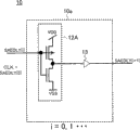
Fig. 2 is the figure of schematic configuration example of the delayed clock circuit 10 of the prior art among the SRAM100 of presentation graphs 1.In Fig. 2,12A is first phase inverter, and 13 is second phase inverters, and the output of the first phase inverter 12A and the input of second phase inverter 13 are connected.As shown in Figure 2, delayed clock circuit 10 is with the first phase inverter 12A and second phase inverter 13 array structure as 1 inscape.That is, delayed clock circuit 10 will have the first and second phase inverter 12A that are connected in series, 13 inscape 10a cascade connection.
Fig. 3 is the figure of schematic configuration example of the delayed clock circuit 16 of the embodiments of the present invention among the SRAM100 of presentation graphs 1.In Fig. 3, except that the prior art constructions shown in Fig. 2, also added the structure of delayed clock control circuit 14.Be that delayed clock circuit 16 is to be formed by connecting having first and second phase inverters 12,13 that are connected in series and the inscape 16a cascade of delayed clock control circuit 14.Delayed clock control circuit 14 is connected on the output node of the link node of first and second phase inverters 12,13 and second phase inverter 13.And, as described later, when changing, the input of inscape 16a carries out work, so that penetrating current flows through the link node of first and second phase inverters 12,13 and charge competition takes place at the fixed time.
And in the structure of Fig. 3, delayed clock control circuit 14 has a P transistor npn npn 15 that receives the output of second phase inverter 13 between the link node that is configured in the power lead VDD and first and second phase inverters 12,13, on grid.In addition, also can replace a P transistor npn npn 15 and a plurality of P transistor npn npns that plural serial stage connects are set.And, phase inverter can also be set to substitute a P transistor npn npn 15.
In addition, in the structure of Fig. 3, first phase inverter 12, a plurality of N transistor npn npn 12a, the 12b that have between the link node that is configured in the ground wire VSS and first and second phase inverters 12,13 and be connected in series by multistage (among the figure being 2 grades).In addition, P type and N transistor npn npn in first and second phase inverters 12,13, quantity can be 1, also can be a plurality of of plural serial stage connection.
Fig. 4 is the timing diagram that is used for illustrating the work when structure at Fig. 1 has adopted the delayed clock circuit 16 of the delayed clock circuit 10 of Fig. 2 and Fig. 3., enumerate the situation of the work of reading herein, relatively and the prior art of Fig. 2 and the present embodiment of Fig. 3 be shown.
With input clock signal CLK line of input code translator 9, the output that activates line decoder 9 is word line WL.Storage unit 8 responds the activation of word line WL and makes bit line produce the small electric potential difference to BL, NBL.On the other hand, with input clock signal CLK input delay clock circuit 10,16.
In the prior art of Fig. 2, when input clock signal CLK becomes High (below, be designated as " H (high level) "), among the first phase inverter 12A P transistor npn npn by, N transistor npn npn conducting, and output Low (below, be designated as " L (low level) ").Therefore, the input to the second secondary phase inverter 13 applies " L ".Thus, the P transistor npn npn becomes conducting, N transistor npn npn and becomes and end in second phase inverter 13, and output " H ".By changing gate circuit progression, can adjust the activation timing of sensor amplifier enable signal SAE.Sensor amplifier 20, the activation of response sensor amplifier enable signal SAE, detection and output bit-line are to the small electric potential difference of BL, NBL.
On the other hand, in the present embodiment of Fig. 3, when input clock signal CLK was " L ", the conducting of P transistor npn npn, N transistor npn npn ended in first phase inverter 12, and output " H ".Therefore, the input to the second secondary phase inverter 13 applies " H ".Thus, the P transistor npn npn becomes by, N transistor npn npn and becomes conducting in second phase inverter 13, and output " L ".The output of second phase inverter 13 " L " is input to the grid of a P transistor npn npn 15 of delayed clock control circuit 14.Consequently, a P transistor npn npn 15 conductings.
When input clock signal CLK was " H ", the P transistor npn npn became by, N transistor npn npn and becomes conducting in first phase inverter 12, and output " L ".At this constantly, therefore the charge competition that the penetrating current by the charge charging of the charge discharge of the N transistor npn npn of first phase inverter 12 and a P transistor npn npn 15 causes, takes place at certain hour in a P transistor npn npn 15 conductings of delayed clock control circuit 14.Afterwards, the input to the second secondary phase inverter 13 applies " L ".Thus, the P transistor npn npn becomes by, N transistor npn npn and becomes conducting in second phase inverter 13, and output " H ".Owing to not only change gate circuit progression but also increased a P transistor npn npn 15 of delayed clock control circuit 14, can the charge competition that be caused by penetrating current take place at certain hour, and the activation that can adjust sensor amplifier enable signal SAE regularly.Sensor amplifier 20, the activation of response sensor amplifier enable signal SAE, detection and output bit-line are to the small electric potential difference of BL, NBL.
As mentioned above, the charge competition that is caused by penetrating current can be taken place by the N transistor npn npn of the P transistor npn npn 15 of delayed clock control circuit 14 and first phase inverter 12 in the delayed clock circuit 16 of the Fig. 3 by adopting present embodiment at certain hour.Thus, compared with prior art the activation of sensor amplifier enable signal SAE further can be postponed.In other words, only append 1 transistor unit, just can be in transistor level deviation, particularly SRAM100 be arranged under the little situation of the driving force driving force big, the N transistor npn npn of P transistor npn npn with the activation of sensor amplifier enable signal SAE than the further delay of prior art, area increases and can not cause significantly.Therefore, can increase the value of bit line, and can suppress to produce the probability that delays work, thereby can improve SRAM and the qualification rate that the SIC (semiconductor integrated circuit) of SRAM is housed the small electric potential difference of BL, NBL.
In addition, take place the schedule time of the charge competition that caused by penetrating current, the rising edge that cans be compared to input clock signal CLK most is short at interval.
In addition, in the delayed clock circuit 16 of Fig. 3, the grid width sum of a plurality of N transistor npn npns that plural serial stage that first phase inverter 12 has connects is preferably more than 2 times of grid width of a P transistor npn npn 15 of delayed clock control circuit 14, below 40 times.When the ratio of this grid width during less than 2 times, the driving force that makes charge discharge of the N transistor npn npn of first phase inverter 12 is poorer than the driving force that makes charge charging of a P transistor npn npn 15 of delayed clock control circuit 14, therefore will cause delayed clock circuit 16 to produce and delay work.On the other hand, when the ratio of this grid width surpasses 40 times, the charge competition that is caused by penetrating current takes place and the effect that makes time delay and increase will almost lose.Therefore, by in the restriction of above-mentioned grid width, designing, can make the activation of sensor amplifier enable signal SAE regularly be optimum value.
Fig. 5 is the figure of schematic configuration example of the delayed clock circuit 19 of the embodiments of the present invention among the SRAM100 of presentation graphs 1.In Fig. 5, except that the prior art constructions shown in Fig. 2, also added the structure of delayed clock control circuit 17.That is, the delayed clock circuit 19 inscape 19a cascade that will have first and second phase inverters 12,13 that are connected in series and a delayed clock control circuit 17 connects.Delayed clock control circuit 17 is connected on the output node of the link node of first and second phase inverters 12,13 and second phase inverter 13.And delayed clock control circuit 17 is compared with the delayed clock control circuit 14 of Fig. 3, except that a P transistor npn npn 15, also has the 2nd P transistor npn npn 18.The 2nd a P transistor npn npn 18 and a P transistor npn npn 15 are configured between the link node of the power lead VDD and first and second phase inverters 12,13 in parallel, and receive the first external signal TE on grid.Promptly according to the first external signal TE control the 2nd P transistor npn npn 18 conducting, end.
Fig. 6 is the timing diagram that is used for illustrating the work when structure at Fig. 1 has adopted the delayed clock circuit 19 of Fig. 5.Enumerate the situation of the work of reading herein.And the first external signal TE describes as the signal that switches work usually and test job.In addition, because the groundwork of SRAM100 is identical with Fig. 4, its explanation is omitted.
In working usually, the first external signal TE is " H ", and the 2nd P transistor npn npn 18 is ended.At this moment, the transistor that in delayed clock control circuit 17 delay clock signals is further postponed only is a P transistor npn npn 15, thereby can obtain the effect identical with the structure of Fig. 3.
In test job, the first external signal TE is " L ", makes 18 conductings of the 2nd P transistor npn npn.At this moment, in delayed clock control circuit 17, except that a P transistor npn npn 15, the 2nd P transistor npn npn 18 also carries out work as the transistor that delay clock signals is further postponed.Thus, compare with the structure of Fig. 3 further increased time delay.
As mentioned above, under the situation of the delayed clock circuit 19 of the Fig. 5 that has adopted present embodiment, when carrying out test job, the charge competition that is caused by penetrating current can take place at certain hour by the N transistor npn npn of the first and second P transistor npn npns 15,18 of delayed clock control circuit 17 and first phase inverter 12.Thus, the activation of sensor amplifier enable signal SAE is further postponed.In other words, just appended 1 transistor unit again, the activation of the sensor amplifier enable signal SAE in the time of just can be with test job further postpones, and area increases and can not cause significantly.Therefore, can increase the value of bit line to the small electric potential difference of BL, NBL, and can suppress to produce the probability of misoperation, thereby can promote SRAM and be equipped with SRAM SIC (semiconductor integrated circuit) the fault detect position determine and the raising of fault detect rate in improve qualification rate.
In addition, the first external signal TE has more than and is defined in the signal that switches work usually and test job.For example, keep " L " with immobilizing, the activation of sensor amplifier enable signal SAE further can be postponed by making the first external signal TE.Therefore, the value of bit line can be increased, and the probability that delays work can be suppressed to produce the small electric potential difference of BL, NBL.
And, in the structure of Fig. 5, also a P transistor npn npn 15 can be omitted.
In addition, in the delayed clock circuit 19 of Fig. 5, the grid width sum of a plurality of N transistor npn npns that plural serial stage that first phase inverter 12 has connects is preferably more than 2 times of grid width sum of the first and second P transistor npn npns 15,18 of delayed clock control circuit 17, below 40 times.When the ratio of this grid width during less than 2 times, the driving force that makes charge discharge of the N transistor npn npn of first phase inverter 12 is poorer than the driving force that makes charge charging of the first and second P transistor npn npns 15,18 of delayed clock control circuit 17, therefore will cause delayed clock circuit 19 to produce and delay work.On the other hand, when the ratio of this grid width surpasses 40 times, the charge competition that is caused by penetrating current takes place and the effect that makes time delay and increase almost loses.Therefore, by in the restriction of above-mentioned grid width, designing, can make the activation of sensor amplifier enable signal SAE regularly be optimum value.
Fig. 7 is the figure of schematic configuration example of the delayed clock circuit 22 of the embodiment of the present invention among the SRAM100 of presentation graphs 1.In Fig. 7, except that the delayed clock circuit 16 of Fig. 3, also added P transistor npn npn substrate control circuit 23 and the N transistor npn npn structure of substrate control circuit 24.The P transistor npn npn with the substrate control circuit 23 response second external signal BE by the substrate electric potential of the P transistor npn npn 15 in the signal VDDBB control lag clock control circuit 14.The N transistor npn npn is controlled the N transistor npn npn 12a in first phase inverter 12, the substrate electric potential of 12b with the substrate control circuit 24 response second external signal BE by signal VSSBB.
Fig. 8 is the timing diagram that is used for illustrating the work when structure at Fig. 1 has adopted the delayed clock circuit 22 of Fig. 7.Enumerate the situation of the work of reading herein.And the second external signal BE describes as the signal that switches work usually and test job.In addition, because the groundwork of SRAM100 is identical with Fig. 4, its explanation is omitted.
In working usually, according to the second external signal BE, the P transistor npn npn be can't help output signal VDDBB to the undercoat biasing of a P transistor npn npn 15 with substrate control circuit 23, and the N transistor npn npn be can't help the undercoat biasing of output signal VSSBB to the N transistor npn npn of first phase inverter 12 with substrate control circuit 24.Therefore, in the threshold voltage of N transistor npn npn 12a, the 12b of a P transistor npn npn 15 and first phase inverter 12, do not change, can obtain the effect identical with Fig. 3.
In test job, according to the second external signal BE, the P transistor npn npn applies forward bias by output signal VDDBB to the substrate of a P transistor npn npn 15 with substrate control circuit 23, and the N transistor npn npn applies reverse biased by output signal VSSBB to the N transistor npn npn 12a of first phase inverter 12, the substrate of 12b with substrate control circuit 24.Thus, the one P transistor npn npn 15, because of reducing to make current driving ability, the absolute value of threshold voltage increases, N transistor npn npn 12a, the 12b of first phase inverter 12, because of the absolute value of threshold voltage increases current driving ability is reduced, therefore, charge competition taking place on link node, thereby makes time delay than the further increase of Fig. 3.
As mentioned above, under the situation of the delayed clock circuit 22 of the Fig. 7 that has adopted present embodiment, when carrying out test job, the absolute value of the threshold voltage of the P transistor npn npn 15 in the delayed clock control circuit 14 is reduced, and the absolute value of the threshold voltage of N transistor npn npn 12a, 12b in first phase inverter 12 is increased.Therefore, the current driving ability of a P transistor npn npn 15 is increased, and the N transistor npn npn 12a of first phase inverter 12, the current driving ability of 12b are reduced, therefore can the charge competition that be caused by penetrating current take place at certain hour.Thus, the activation of the sensor amplifier enable signal SAE in the time of can be with test job further postpones.Therefore, can increase the value of bit line to the small electric potential difference of BL, NBL, and can suppress to produce the probability of misoperation, thereby can promote SRAM and be equipped with SRAM SIC (semiconductor integrated circuit) the fault detect position determine and the raising of fault detect rate in improve qualification rate.
In addition, the second external signal BE has more than and is defined in the signal that switches work usually and test job.For example, also can apply forward bias, the N transistor npn npn 12a of first phase inverter 12, the substrate of 12b are applied reverse biased the substrate of a P transistor npn npn 15 with immobilizing according to the second external signal BE.Thus, the activation of sensor amplifier enable signal SAE further can be postponed, and can increase the value of bit line, and can suppress to produce the probability of misoperation the small electric potential difference of BL, NBL.In addition, in Fig. 7, any in P transistor npn npn usefulness substrate control circuit 23 or the N transistor npn npn usefulness substrate control circuit 24 can only be set also.
Fig. 9 is the circuit diagram of the schematic configuration example of the line decoder among the SRAM100 of presentation graphs 1.In Fig. 9, line decoder 9 is when being selected by address signal AD, to word line WL output pulse signal.Input clock signal CLK generates the pulse edge to the upthrow side of the pulse signal of word line WL output.Word line pulse generates the pulse edge that signal PLSDLY generates the decline side of the pulse signal that word line WL is exported.And line decoder 9 receives from the delay clock signals of delayed clock circuit 16,19,22 outputs and generates signal PLSDLY as word line pulse.
Figure 10 is the timing diagram of work of SRAM100 that is used to illustrate Fig. 1 of the line decoder that comprises Fig. 9.Enumerate the situation of the work of reading herein.And, in Figure 10, the action when common work and sensor amplifier enable signal SAE delay is shown.Herein, usually work is the work timing that configures when design, and is different therewith, when various conditions such as technology, voltage, temperature, frequency have produced when departing from, sensor amplifier enable signal SAE postponed.
In Figure 10, with input clock signal CLK line of input code translator 9, the output that activates line decoder 9 is word line WL.Storage unit 8 responds the activation of word line WL and makes bit line produce the small electric potential difference to BL, NBL.On the other hand, with input clock signal CLK input delay clock circuit 16,19,22.Sensor amplifier 20, response are as the activation of the sensor amplifier enable signal SAE of the output of delayed clock circuit 16,19,22, and detection and output bit-line are to the small electric potential difference of BL, NBL.
The output of line decoder 9 is word line WL, generates signal PLSDLY according to the word line pulse as the output of delayed clock circuit 16,19,22 and becomes unactivated state.Owing to generate signal PLSDLY from delayed clock circuit 16,19, the 22 output sensor amplifier enable signal SAE and the word line pulse of same type, even having produced, various condition departs from, each regularly also demonstrates same tendency to departing from of condition.Therefore, when sensor amplifier enable signal SAE was postponed, word line pulse generated signal PLSDLY and postpones similarly.Thus, pulse width that can broadening word line WL.
As mentioned above, according to the structure of Fig. 1 and Fig. 9, word line pulse generates signal PLSDLY and sensor amplifier enable signal SAE, and it regularly departs from condition and demonstrates same tendency.Therefore, when sensor amplifier enable signal SAE was postponed, word line pulse generated signal PLSDLY and postpones similarly, and the pulse width of energy broadening word line WL.So, bit line is increased the small electric potential difference of BL, NBL, and can suppress to produce the probability that delays work, thereby can improve SRAM and the qualification rate that the SIC (semiconductor integrated circuit) of SRAM is housed.
In addition, sensor amplifier enable signal SAE and word line pulse generate signal PLSDLY, are the output from the delayed clock circuit 16,19,22 of same type, but also not necessarily from identical gate circuit progression output.
Figure 11 is the figure of the schematic configuration example of the copied rows code translator (RDR) 29 among the SRAM100 of presentation graphs 1.In Figure 11, copied rows code translator 29 is made of the structure identical with line decoder 9, and receiver address signal AD but as selecteed all the time not receives supply voltage VDD or is the signal of benchmark with supply voltage VDD.That is, with by the identical timing of the selected line decoder of address signal AD 9, output pulse signal is as wordline delay signal WLDLY.Wordline delay signal WLDLY from 29 outputs of copied rows code translator is input to delayed clock circuit 16,19,22 as input clock signal.
As mentioned above, according to the structure of Figure 11,, be activated with the roughly the same timing of word line WL from the wordline delay signal WLDLY of copied rows code translator 29 outputs that constitute by the structure identical with line decoder 9.Therefore, can suppress to be input to the deviation of the timing of delayed clock circuit 16,19,22.In addition, also word line pulse can be generated signal PLSDLY omits.
Figure 12 is illustrated in the timing diagram that has adopted the work when duplicating storage unit 32 among the SRAM100 of Fig. 1.In Fig. 1, duplicate memory cell array 36 row shapes and dispose and a plurality ofly duplicate storage unit 32 by what the structure identical with storage unit 8 constituted.And, the row setting of duplicating storage unit 32 is duplicated bit line to RBL, RNBL.In addition, duplicate storage unit inhibit signal MEMDLY, be meant to be shown in and duplicate bit line to whether having produced the signal of predetermined potential difference (PD) on RBL, the RNBL, supposition herein is " H " when duplicating bit line and produced predetermined potential difference (PD) on to RBL, RNBL.In addition, replace the first external signal TE on the grid of the 2nd P transistor npn npn 18 of delayed clock circuit 19 in delayed clock control circuit 17 and receive and duplicate storage unit inhibit signal MEMDLY.
According to the structure of Fig. 1, can be by the deviation of duplicating storage unit 32 reflection storage unit 8.Therefore, as shown in figure 12, when storage unit 8 and the electric charge that duplicates storage unit 32 are drawn when fast, the timing advance that the 2nd P transistor npn npns 18 in the delayed clock circuit 19 are ended, therefore the timing by sensor amplifier enable signal SAE starting sensor amplifier 20 also shifts to an earlier date.On the other hand, when storage unit 8 and the electric charge that duplicates storage unit 32 are drawn when slow, make the 2nd P transistor npn npn 18 conductings in the delayed clock circuit 19 during prolong, make its constant time lag of ending, therefore also make constant time lag by sensor amplifier enable signal SAE starting sensor amplifier 20.
Like this, regardless of the standard deviation of storage unit 8, can therefore, qualification rate be improved having guaranteed to make sensor amplifier 20 startings under the state of bit line to the small electric potential difference of BL, NBL fully.
Figure 13 is the figure of the schematic configuration example that writes auxiliary circuit 50 among the SRAM100 of presentation graphs 1.In the structure of Figure 13,, use the P transistor npn npn to draw electric charge for the voltage that does not make power supply 51 descends lowly excessively.In Fig. 1, the row that write 50 pairs of storage unit 8 of auxiliary circuit are provided with, write auxiliary pulse signal PWPLS output pulse during, the current potential of power supply 51 is reduced.Write auxiliary pulse signal PWPLS, generate signal PWDLY and generate by write-enable signal WE with as the pulse that writes from the delay clock signals of delayed clock circuit 16,19,22 output.Write pulse and generate the pulse edge that signal PWDLY generation writes auxiliary pulse signal PWPLS.
Figure 14 is illustrated in the timing diagram that has adopted the work when writing auxiliary circuit 50 among the SRAM100 of Fig. 1.As mentioned above, as the input signal that writes auxiliary circuit 50 write auxiliary pulse signal PWPLS, its pulse edge generates signal PWDLY5 and generates by writing pulse.Herein, writing the process deviation that is difficult to most to carry out, be that the driving force of P transistor npn npn is big and under the situation that the driving force of N transistor npn npn is little, delayed clock circuit 16,19,22 is compared with the delay circuit 10 of prior art, can make the constant time lag of activation.Therefore, write the activation that pulse generates signal PWDLY and be delayed, institute is so that write the pulse width increase of auxiliary pulse signal PWPLS.Thus, can make current potential reduction, be easy to carry out thereby make to write as the power supply 51 of the output that writes auxiliary circuit 50.
Figure 15 is the figure of schematic configuration example of layout of the SRAM100 of presentation graphs 1.In Figure 15, the 16, the 19th, the delayed clock circuit, the 30th, memory cell array, the 40th, the line decoder array, the 70th, arrange the read/write circuit array of a plurality of read/write circuits by the row shape, the 80th, signal control circuit.Delayed clock control circuit 14,17, be configured in the distance of memory cell array 30, line decoder array 40, read/write circuit array 70 than with the position of the distance of delayed clock circuit 16,19.
Shown in the structure of Figure 15, by delayed clock control circuit 14,17 is configured in the signal control circuit 80, can suppress the increase of layout area, and can guarantee interconnection resource line decoder array 40 and read/write circuit array 70.
Figure 16 and Figure 17 are the figure of schematic configuration example of layout of the delayed clock circuit 16a of presentation graphs 3 and Fig. 7.In Figure 16 and Figure 17, be defined as the grid width direction, the vertical direction of grid width direction be defined as the grid length direction as bearing of trend gate electrode, then in delayed clock circuit 16a with the source electrode of the source electrode of the P transistor npn npn of first phase inverter 12 and drain electrode and the P transistor npn npn of second phase inverter 13 and drain electrode general layout point-blank.In addition, the source electrode of a P transistor npn npn 15 that also source electrode of the P transistor npn npn of second phase inverter 13 and drain electrode and delayed clock control circuit 14,17 is had and drain electrode general layout are point-blank.
As mentioned above, according to the structure of Figure 16 and Figure 17, diffusion zone along the grid length direction by general layout point-blank.Thus, can lower the characteristics of transistor deviation.Therefore, can suppress from the timing offset of the signal of delayed clock circuit 16a output.
Figure 18 is the figure of schematic configuration example of layout of the delayed clock circuit 16a of presentation graphs 3 and Fig. 7.In Figure 18, be defined as the grid width direction, the vertical direction of grid width direction be defined as the grid length direction as bearing of trend gate electrode, then in delayed clock circuit 16a with the source electrode of the source electrode of the P transistor npn npn of first phase inverter 12 and drain electrode and the P transistor npn npn of second phase inverter 13 and drain electrode general layout point-blank.In addition, the source electrode of a P transistor npn npn 15 that also source electrode of the P transistor npn npn of first phase inverter 12 and drain electrode and delayed clock control circuit 14,17 is had and drain electrode general layout are point-blank.
As mentioned above, according to the structure of Figure 18, diffusion zone along the grid length direction by general layout point-blank.Thus, can lower the characteristics of transistor deviation.Therefore, can suppress from the timing offset of the signal of delayed clock circuit 16a output.
In addition, the present invention is not limited to above-mentioned embodiment, can implement various changes in the scope that does not break away from its purport.For example,, be illustrated herein, but in DRAM or other semiconductor storage, also can be out of shape and implement with SRAM.
According to the present invention, can make SIC (semiconductor integrated circuit) have transistor level deviation permission and can not cause the increase of circuit area.Therefore, for example, as the semiconductor storage that comprises sensor amplifier, particularly SRAM, in detail, the cache memory used as microprocessor etc. is useful.
Claims (15)
1. SIC (semiconductor integrated circuit) is characterized in that:
Have the delayed clock circuit that input clock signal is postponed,
The inscape with first phase inverter and second phase inverter of above-mentioned delayed clock circuit is cascaded and is connected,
Above-mentioned each inscape has the delayed clock control circuit, and it carries out work when input changes, so that penetrating current flows through the link node of above-mentioned first phase inverter and above-mentioned second phase inverter and charge competition takes place at the fixed time.
2. SIC (semiconductor integrated circuit) according to claim 1 is characterized in that:
The above-mentioned schedule time is shorter at interval than the rising edge of above-mentioned input clock signal.
3. SIC (semiconductor integrated circuit) according to claim 1 is characterized in that:
Above-mentioned delayed clock control circuit has a P transistor npn npn that is configured between power lead and the above-mentioned link node and receives the output of above-mentioned second phase inverter on grid,
Above-mentioned first phase inverter has a plurality of N transistor npn npns that are configured between ground wire and the above-mentioned link node and are connected by plural serial stage.
4. SIC (semiconductor integrated circuit) according to claim 3 is characterized in that:
The grid width sum of above-mentioned a plurality of N transistor npn npns is more than 2 times below 40 times of grid width of an above-mentioned P transistor npn npn.
5. SIC (semiconductor integrated circuit) according to claim 3 is characterized in that:
Above-mentioned delayed clock control circuit has the 2nd P transistor npn npn that is configured between power lead and the above-mentioned link node and receives first external signal on grid.
6. SIC (semiconductor integrated circuit) according to claim 5 is characterized in that:
The grid width sum of above-mentioned a plurality of N transistor npn npns is more than 2 times below 40 times of grid width sum of the above-mentioned first and second P transistor npn npns.
7. SIC (semiconductor integrated circuit) according to claim 5 is characterized in that:
Above-mentioned first external signal is the signal that switches work usually and test job, and above-mentioned first external signal makes above-mentioned the 2nd P transistor npn npn conducting when test job.
8. SIC (semiconductor integrated circuit) according to claim 3 is characterized in that:
Above-mentioned delayed clock circuit also has the substrate control circuit of controlling the substrate electric potential of an above-mentioned P transistor npn npn and above-mentioned a plurality of N transistor npn npns according to second external signal.
9. SIC (semiconductor integrated circuit) according to claim 8 is characterized in that:
Above-mentioned second external signal is the signal that is used to switch common work and test job,
Above-mentioned substrate control circuit applies forward bias to the substrate of an above-mentioned P transistor npn npn, and the substrate of above-mentioned a plurality of N transistor npn npns is applied reverse biased when test job.
10. SIC (semiconductor integrated circuit) according to claim 1 is characterized in that:
Have
Be the rectangular memory cell array that is arranged with a plurality of storage unit,
Respectively many word lines that the row of said memory cells array is provided with,
Respectively a plurality of bit lines that the row of said memory cells array are provided with to,
The sensor amplifier that small electric potential difference that above-mentioned bit line is right is amplified and
When by address signal when selected to the line decoder of above-mentioned word line output pulse signal,
Above-mentioned sensor amplifier receives delay clock signals from above-mentioned delayed clock circuit output as the sensor amplifier enable signal,
The above line code translator receives from the delay clock signals of above-mentioned delayed clock circuit output and generates signal as the word line pulse of the pulse edge that generates above-mentioned pulse signal.
11. SIC (semiconductor integrated circuit) according to claim 10 is characterized in that:
Have by the structure identical with the above line code translator constitute, receiver address signal and not by the copied rows code translator of the timing output pulse signal identical with selected above line code translator,
Be used as above-mentioned input clock signal and import above-mentioned delayed clock circuit from the above-mentioned pulse signal of above-mentioned copied rows code translator output.
12. SIC (semiconductor integrated circuit) according to claim 5 is characterized in that:
Have
Be the rectangular memory cell array that is arranged with a plurality of storage unit,
Respectively many word lines that the row of said memory cells array is provided with,
Respectively a plurality of bit lines that the row of said memory cells array are provided with to,
The sensor amplifier that the small electric potential difference that above-mentioned bit line is right is amplified,
Be the row shape be arranged with a plurality of by the structure identical with said memory cells constitute duplicate storage unit duplicate memory cell array and
To above-mentioned row setting of duplicating storage unit to duplicate bit line right,
Above-mentioned sensor amplifier receives delay clock signals from above-mentioned delayed clock circuit output as the sensor amplifier enable signal,
On the grid of above-mentioned the 2nd P transistor npn npn of above-mentioned delayed clock circuit in above-mentioned delayed clock control circuit, do not receive above-mentioned first external signal and receive to be used in reference to and be shown in the above-mentioned bit line that duplicates the last signal that whether has produced predetermined potential difference (PD).
13. SIC (semiconductor integrated circuit) according to claim 1 is characterized in that:
Have
Be the rectangular memory cell array that is arranged with a plurality of storage unit,
The row of said memory cells array are provided with, above-mentioned write auxiliary pulse signal output pulse during make the auxiliary circuit that writes that the current potential of the power supply of said memory cells reduces,
The above-mentioned pulse edge that writes auxiliary pulse signal is generated by the delay clock signals from above-mentioned delayed clock circuit output.
14. SIC (semiconductor integrated circuit) according to claim 3 is characterized in that:
In above-mentioned delayed clock circuit,
The source electrode of the P transistor npn npn of the source electrode of the P transistor npn npn of above-mentioned first phase inverter and drain electrode and above-mentioned second phase inverter and the drain electrode roughly point-blank by layout, and
The source electrode of the above-mentioned P transistor npn npn that the source electrode of the P transistor npn npn of above-mentioned second phase inverter and drain electrode and above-mentioned delayed clock control circuit have and drain electrode are roughly by layout point-blank.
15. SIC (semiconductor integrated circuit) according to claim 3 is characterized in that:
In above-mentioned delayed clock circuit,
The source electrode of the P transistor npn npn of the source electrode of the P transistor npn npn of above-mentioned first phase inverter and drain electrode and above-mentioned second phase inverter and the drain electrode by general layout point-blank, and
The source electrode of the above-mentioned P transistor npn npn that the source electrode of the P transistor npn npn of above-mentioned first phase inverter and drain electrode and above-mentioned delayed clock control circuit have and drain electrode are roughly by layout point-blank.
Applications Claiming Priority (2)
| Application Number | Priority Date | Filing Date | Title |
|---|---|---|---|
| JP2007051170 | 2007-03-01 | ||
| JP2007051170A JP2008219232A (en) | 2007-03-01 | 2007-03-01 | Semiconductor integrated circuit |
Publications (1)
| Publication Number | Publication Date |
|---|---|
| CN101256824A true CN101256824A (en) | 2008-09-03 |
Family
ID=39732670
Family Applications (1)
| Application Number | Title | Priority Date | Filing Date |
|---|---|---|---|
| CNA2008100809379A Pending CN101256824A (en) | 2007-03-01 | 2008-02-29 | Semiconductor integrated circuit |
Country Status (3)
| Country | Link |
|---|---|
| US (1) | US20080211556A1 (en) |
| JP (1) | JP2008219232A (en) |
| CN (1) | CN101256824A (en) |
Cited By (6)
| Publication number | Priority date | Publication date | Assignee | Title |
|---|---|---|---|---|
| CN103226982A (en) * | 2012-01-30 | 2013-07-31 | 精工电子有限公司 | Semiconductor device including semiconductor memory circuit |
| WO2022110697A1 (en) * | 2020-11-25 | 2022-06-02 | 长鑫存储技术有限公司 | Control circuit and delay circuit |
| US11528020B2 (en) | 2020-11-25 | 2022-12-13 | Changxin Memory Technologies, Inc. | Control circuit and delay circuit |
| US11550350B2 (en) | 2020-11-25 | 2023-01-10 | Changxin Memory Technologies, Inc. | Potential generating circuit, inverter, delay circuit, and logic gate circuit |
| US11681313B2 (en) | 2020-11-25 | 2023-06-20 | Changxin Memory Technologies, Inc. | Voltage generating circuit, inverter, delay circuit, and logic gate circuit |
| US11887652B2 (en) | 2020-11-25 | 2024-01-30 | Changxin Memory Technologies, Inc. | Control circuit and delay circuit |
Families Citing this family (1)
| Publication number | Priority date | Publication date | Assignee | Title |
|---|---|---|---|---|
| CN110956990B (en) * | 2018-09-26 | 2022-03-01 | 展讯通信(上海)有限公司 | SRAM reading delay control circuit and SRAM |
Family Cites Families (25)
| Publication number | Priority date | Publication date | Assignee | Title |
|---|---|---|---|---|
| JP3071915B2 (en) * | 1991-12-20 | 2000-07-31 | 株式会社東芝 | Output circuit |
| US5424985A (en) * | 1993-06-30 | 1995-06-13 | Sgs-Thomson Microelectronics, Inc. | Compensating delay element for clock generation in a memory device |
| US5841300A (en) * | 1994-04-18 | 1998-11-24 | Hitachi, Ltd. | Semiconductor integrated circuit apparatus |
| US6590423B1 (en) * | 1994-10-11 | 2003-07-08 | Derek Wong | Digital circuits exhibiting reduced power consumption |
| US5517136A (en) * | 1995-03-03 | 1996-05-14 | Intel Corporation | Opportunistic time-borrowing domino logic |
| US5661675A (en) * | 1995-03-31 | 1997-08-26 | Intel Corporation | Positive feedback circuit for fast domino logic |
| US6104213A (en) * | 1998-03-02 | 2000-08-15 | International Business Machines Corporation | Domino logic circuit having a clocked precharge |
| US6097207A (en) * | 1998-08-21 | 2000-08-01 | International Business Machines Corporation | Robust domino circuit design for high stress conditions |
| JP3358612B2 (en) * | 1999-03-15 | 2002-12-24 | 日本電気株式会社 | Semiconductor integrated circuit |
| JP3241686B2 (en) * | 1999-03-26 | 2001-12-25 | 日本電気株式会社 | Dynamic logic circuit and domino logic element |
| US6137319A (en) * | 1999-04-30 | 2000-10-24 | Intel Corporation | Reference-free single ended clocked sense amplifier circuit |
| US6346831B1 (en) * | 1999-09-28 | 2002-02-12 | Intel Corporation | Noise tolerant wide-fanin domino circuits |
| US6549040B1 (en) * | 2000-06-29 | 2003-04-15 | Intel Corporation | Leakage-tolerant keeper with dual output generation capability for deep sub-micron wide domino gates |
| US6469953B1 (en) * | 2001-08-08 | 2002-10-22 | Intel Corporation | Latch circuit |
| US6429689B1 (en) * | 2001-10-10 | 2002-08-06 | International Business Machines Corporation | Method and apparatus for controlling both active and standby power in domino circuits |
| US6933744B2 (en) * | 2002-06-11 | 2005-08-23 | The Regents Of The University Of Michigan | Low-leakage integrated circuits and dynamic logic circuits |
| US7218151B1 (en) * | 2002-06-28 | 2007-05-15 | University Of Rochester | Domino logic with variable threshold voltage keeper |
| JP2004048313A (en) * | 2002-07-11 | 2004-02-12 | Matsushita Electric Ind Co Ltd | Dynamic circuit |
| US6765414B2 (en) * | 2002-09-17 | 2004-07-20 | Intel Corporation | Low frequency testing, leakage control, and burn-in control for high-performance digital circuits |
| US7034576B2 (en) * | 2003-06-27 | 2006-04-25 | Sun Microsystems, Inc. | Pulsed dynamic keeper gating |
| US7202705B2 (en) * | 2004-10-14 | 2007-04-10 | International Business Machines Corporation | Dynamic logic circuit apparatus and method for reducing leakage power consumption via separate clock and output stage control |
| US7282960B2 (en) * | 2005-06-28 | 2007-10-16 | International Business Machines Corporation | Dynamic logical circuit having a pre-charge element separately controlled by a voltage-asymmetric clock |
| JP2007096907A (en) * | 2005-09-29 | 2007-04-12 | Matsushita Electric Ind Co Ltd | Semiconductor integrated circuit |
| US7764087B2 (en) * | 2006-02-01 | 2010-07-27 | Wisconsin Alumni Research Foundation | Low swing domino logic circuits |
| US7332938B2 (en) * | 2006-06-23 | 2008-02-19 | The Curators Of The University Of Missouri | Domino logic testing systems and methods |
-
2007
- 2007-03-01 JP JP2007051170A patent/JP2008219232A/en not_active Withdrawn
-
2008
- 2008-02-07 US US12/027,411 patent/US20080211556A1/en not_active Abandoned
- 2008-02-29 CN CNA2008100809379A patent/CN101256824A/en active Pending
Cited By (7)
| Publication number | Priority date | Publication date | Assignee | Title |
|---|---|---|---|---|
| CN103226982A (en) * | 2012-01-30 | 2013-07-31 | 精工电子有限公司 | Semiconductor device including semiconductor memory circuit |
| CN103226982B (en) * | 2012-01-30 | 2017-03-01 | 精工半导体有限公司 | There is the semiconductor device of semiconductor memory circuit |
| WO2022110697A1 (en) * | 2020-11-25 | 2022-06-02 | 长鑫存储技术有限公司 | Control circuit and delay circuit |
| US11528020B2 (en) | 2020-11-25 | 2022-12-13 | Changxin Memory Technologies, Inc. | Control circuit and delay circuit |
| US11550350B2 (en) | 2020-11-25 | 2023-01-10 | Changxin Memory Technologies, Inc. | Potential generating circuit, inverter, delay circuit, and logic gate circuit |
| US11681313B2 (en) | 2020-11-25 | 2023-06-20 | Changxin Memory Technologies, Inc. | Voltage generating circuit, inverter, delay circuit, and logic gate circuit |
| US11887652B2 (en) | 2020-11-25 | 2024-01-30 | Changxin Memory Technologies, Inc. | Control circuit and delay circuit |
Also Published As
| Publication number | Publication date |
|---|---|
| JP2008219232A (en) | 2008-09-18 |
| US20080211556A1 (en) | 2008-09-04 |
Similar Documents
| Publication | Publication Date | Title |
|---|---|---|
| CN1870175B (en) | Semiconductor memory device | |
| CN100594556C (en) | SRAM stable against various process-voltage-temperature variations | |
| CN101253569B (en) | Integrated circuit with separate supply voltage for memory that is different from logic circuit supply voltage | |
| CN101256824A (en) | Semiconductor integrated circuit | |
| CN101667452A (en) | Semiconductor device | |
| US8050082B2 (en) | Two-stage 8T SRAM cell design | |
| US8391097B2 (en) | Memory word-line driver having reduced power consumption | |
| CN101783168A (en) | Semiconductor integrated circuit device and operating method thereof | |
| KR100518398B1 (en) | Semiconductor memory and control method | |
| US9373389B2 (en) | Semiconductor memory device | |
| US20130258794A1 (en) | Memory device having control circuitry for sense amplifier reaction time tracking | |
| US8625370B2 (en) | Semiconductor integrated circuit | |
| CN100555448C (en) | Semiconductor memory devices and time control method | |
| US6294404B1 (en) | Semiconductor integrated circuit having function of reducing a power consumption and semiconductor integrated circuit system comprising this semiconductor integrated circuit | |
| CN101388244B (en) | Semiconductor integrated circuit | |
| JP2008219232A5 (en) | ||
| CN103620687A (en) | Semiconductor storage device | |
| US8830771B2 (en) | Memory device having control circuitry configured for clock-based write self-time tracking | |
| JP2001176287A (en) | Semiconductor memory and its read-out method | |
| JP2010176742A (en) | Semiconductor device and data processing system | |
| US20100220534A1 (en) | Memory Device with Reduced Buffer Current During Power-Down Mode | |
| JP2016115376A (en) | Bit line pre-charge circuit, static ram, electronic device, and method for static-ram bit line pre-charge | |
| JP2009230787A (en) | Memory device and memory control method | |
| JP5057744B2 (en) | Semiconductor integrated circuit device | |
| JP3087693B2 (en) | Semiconductor storage device |
Legal Events
| Date | Code | Title | Description |
|---|---|---|---|
| C06 | Publication | ||
| PB01 | Publication | ||
| C10 | Entry into substantive examination | ||
| SE01 | Entry into force of request for substantive examination | ||
| C02 | Deemed withdrawal of patent application after publication (patent law 2001) | ||
| WD01 | Invention patent application deemed withdrawn after publication |
Application publication date: 20080903 |