CN100557810C - Solid state image pickup device and imaging device - Google Patents
Solid state image pickup device and imaging device Download PDFInfo
- Publication number
- CN100557810C CN100557810C CNB200710153178XA CN200710153178A CN100557810C CN 100557810 C CN100557810 C CN 100557810C CN B200710153178X A CNB200710153178X A CN B200710153178XA CN 200710153178 A CN200710153178 A CN 200710153178A CN 100557810 C CN100557810 C CN 100557810C
- Authority
- CN
- China
- Prior art keywords
- lens
- layer
- solid state
- image pickup
- state image
- Prior art date
- Legal status (The legal status is an assumption and is not a legal conclusion. Google has not performed a legal analysis and makes no representation as to the accuracy of the status listed.)
- Expired - Fee Related
Links
- 238000003384 imaging method Methods 0.000 title claims abstract description 42
- 239000007787 solid Substances 0.000 title claims abstract description 34
- 230000003287 optical effect Effects 0.000 claims abstract description 33
- 238000006243 chemical reaction Methods 0.000 claims abstract description 24
- 239000000758 substrate Substances 0.000 claims abstract description 20
- 239000004065 semiconductor Substances 0.000 claims abstract description 11
- 206010070834 Sensitisation Diseases 0.000 claims description 19
- 230000008313 sensitization Effects 0.000 claims description 19
- 238000012545 processing Methods 0.000 claims description 18
- 239000003086 colorant Substances 0.000 claims description 6
- 239000010410 layer Substances 0.000 description 23
- 210000002469 basement membrane Anatomy 0.000 description 12
- 238000009826 distribution Methods 0.000 description 12
- 239000011229 interlayer Substances 0.000 description 9
- 230000002093 peripheral effect Effects 0.000 description 8
- 238000010276 construction Methods 0.000 description 7
- XUIMIQQOPSSXEZ-UHFFFAOYSA-N Silicon Chemical compound [Si] XUIMIQQOPSSXEZ-UHFFFAOYSA-N 0.000 description 6
- 238000010586 diagram Methods 0.000 description 6
- 229910052710 silicon Inorganic materials 0.000 description 6
- 239000010703 silicon Substances 0.000 description 6
- 238000003860 storage Methods 0.000 description 6
- 230000005540 biological transmission Effects 0.000 description 5
- 239000000463 material Substances 0.000 description 4
- 229910052814 silicon oxide Inorganic materials 0.000 description 4
- 238000004891 communication Methods 0.000 description 2
- 238000009792 diffusion process Methods 0.000 description 2
- 238000007667 floating Methods 0.000 description 2
- 238000005457 optimization Methods 0.000 description 2
- 230000015572 biosynthetic process Effects 0.000 description 1
- 238000013461 design Methods 0.000 description 1
- 238000001514 detection method Methods 0.000 description 1
- 230000000694 effects Effects 0.000 description 1
- 238000005516 engineering process Methods 0.000 description 1
- 238000005530 etching Methods 0.000 description 1
- 238000004519 manufacturing process Methods 0.000 description 1
- 238000012986 modification Methods 0.000 description 1
- 230000004048 modification Effects 0.000 description 1
- 238000012544 monitoring process Methods 0.000 description 1
- 230000002265 prevention Effects 0.000 description 1
- 238000005070 sampling Methods 0.000 description 1
- 238000012546 transfer Methods 0.000 description 1
Images


Classifications
-
- H—ELECTRICITY
- H01—ELECTRIC ELEMENTS
- H01L—SEMICONDUCTOR DEVICES NOT COVERED BY CLASS H10
- H01L27/00—Devices consisting of a plurality of semiconductor or other solid-state components formed in or on a common substrate
- H01L27/14—Devices consisting of a plurality of semiconductor or other solid-state components formed in or on a common substrate including semiconductor components sensitive to infrared radiation, light, electromagnetic radiation of shorter wavelength or corpuscular radiation and specially adapted either for the conversion of the energy of such radiation into electrical energy or for the control of electrical energy by such radiation
- H01L27/144—Devices controlled by radiation
- H01L27/146—Imager structures
- H01L27/14601—Structural or functional details thereof
- H01L27/14625—Optical elements or arrangements associated with the device
- H01L27/14627—Microlenses
-
- H—ELECTRICITY
- H01—ELECTRIC ELEMENTS
- H01L—SEMICONDUCTOR DEVICES NOT COVERED BY CLASS H10
- H01L27/00—Devices consisting of a plurality of semiconductor or other solid-state components formed in or on a common substrate
- H01L27/14—Devices consisting of a plurality of semiconductor or other solid-state components formed in or on a common substrate including semiconductor components sensitive to infrared radiation, light, electromagnetic radiation of shorter wavelength or corpuscular radiation and specially adapted either for the conversion of the energy of such radiation into electrical energy or for the control of electrical energy by such radiation
- H01L27/144—Devices controlled by radiation
- H01L27/146—Imager structures
- H01L27/148—Charge coupled imagers
Abstract
A kind of solid state image pickup device and imaging device with it, this solid state image pickup device comprises: semiconductor substrate, it is provided with a plurality of pixels, and each pixel has photoelectric conversion section; Multilayer insulating film is layered on the semiconductor substrate; Wiring film is arranged between the multilayer insulating film; Lens in the layer are for each photoelectric conversion section is arranged between the multilayer insulating film; Optical filter is for each photoelectric conversion section is arranged on the dielectric film; And lens on the sheet, for each photoelectric conversion section is arranged on the optical filter, in its middle level on lens and the sheet in the lens at least one each pixel that is characterized as according to optical filter have different structures.
Description
Technical field
The imaging device that comprises this solid state image pickup device that the present invention relates to a kind of solid state image pickup device and also relate to a kind of for example camera or portable phone, this solid state image pickup device is such as the cmos image sensor that comprises such as the optical filter of the color filter that has the different wave length feature for a plurality of pixels.
Background technology
Past provides in cmos image sensor and has had the solid state image pickup device of formation corresponding to lens (on-chip lens) on lens or the sheet in the layer on the lenticule surface of the sensitization part of each pixel.For example, a plurality of wiring layers and interlayer insulating film are laminated in to have on photodiode and the transistorized semiconductor substrate, and lens are arranged between them in the layer.In addition, color filter and lenticule pass through planarization film (flattening film) (for example, with reference to JP-A-2004-304148) disposed thereon on the sheet.
Figure 12 and Figure 13 are the profiles that the example of the laminated construction in the cmos image sensor in the past is shown.
In the figure, the sensitization part 211 of the photodiode of a plurality of pixels is arranged in the top section of silicon substrate 200.Notice that the pixel transistor circuit that is included in each pixel has been omitted in Figure 12 and Figure 13.
Planarization film (interlayer dielectric) 216 and distribution 210 are arranged on the upper surface of silicon substrate 200 by gate insulating film 200A and gate electrode (not shown), and interlayer lens 209 are provided with thereon.Two-layer planarization film (interlayer dielectric) 215 and 214 and distribution 208 and 206 is provided with thereon and uppermost planarization film 213 is provided with thereon.
Then, be arranged on the planarization film 213 corresponding to color of pixel filter 202,203 and 204 separately.Notice that Figure 12 illustrates the section of the position of red filter 202 and 203 appearance of green filter, Figure 13 illustrates the section of the position of green filter 203 and 204 appearance of blue filter.
Summary of the invention
By the way, in above-mentioned cmos image sensor, many wiring films are arranged on the sensitization part, and the distance between uppermost lenticule (top lens) and the photographic department branch increases.Then, the light collection status of the pixel of different colours can not be optimised according to the difference of the optical wavelength of passing through optical filter.Therefore, because the aperture of camera lens and/or, different at center and peripheral sensitization light collection status partly in the difference of the incidence angle of center and peripheral sensitization part.As a result, can take place that for example colored shadow is unbalanced.
The situation as lens in the layer in the example in the past also is.
Therefore, expectation provides the solid state image pickup device and the imaging device of the feature that can optimize the light that is input to the sensitization part that is arranged at the optical filter in each pixel.
According to embodiments of the invention, the solid state image pickup device that comprises the semiconductor substrate which is provided with a plurality of pixels is provided, each pixel has photoelectric conversion section, multilayer insulating film is layered on the semiconductor substrate, wiring film is arranged between the multilayer insulating film, the interlayer lens of each photoelectric conversion section are arranged between the multilayer insulating film, the optical filter of each photoelectric conversion section is arranged on the dielectric film, and lens are arranged on the optical filter on the sheet of each photoelectric conversion section, in its middle level in lens and the sheet lens at least one feature according to optical filter each pixel is had different structures.
According to another embodiment of the invention, provide imaging device, this imaging device comprises: solid state image pickup device, to object image-forming; Imaging optical system forms subject image in the sensitization part of solid state image pickup device; Driving/control section is driven into image optical system; Signal processing is to carrying out signal processing and produce picture signal from the output signal of solid state image pickup device; Recording section, the picture signal that record is produced by signal processing; Output, the picture signal that output is produced by signal processing; And operation part, the signal of input control imaging operation, wherein solid state image pickup device comprises the semiconductor substrate which is provided with a plurality of pixels, each pixel has photoelectric conversion section, multilayer insulating film is layered on the semiconductor substrate, wiring film is arranged between the multilayer insulating film, the interlayer lens of each photoelectric conversion section are arranged between the multilayer insulating film, the optical filter of each photoelectric conversion section is arranged on the dielectric film, and lens are arranged on the optical filter on the sheet of each photoelectric conversion section, in its middle level on lens and the sheet in the lens at least one feature according to optical filter each pixel is had different structures.
Solid state image pickup device and imaging device can be optimized the feature of the light of the sensitization part that is input to the optical filter that is provided with into each pixel according to an embodiment of the invention because in the layer on lens and the sheet lens according to the feature of optical filter each pixel is had different structures.
Description of drawings
Fig. 1 illustrates the profile of the laminated construction of cmos image sensor according to an embodiment of the invention;
Fig. 2 illustrates the profile of the laminated construction of cmos image sensor according to an embodiment of the invention;
Fig. 3 is the block diagram of the cmos image sensor shown in schematically illustrated Fig. 1;
Fig. 4 is the circuit diagram that the pixel structure of the cmos image sensor shown in Fig. 1 is shown;
Fig. 5 is the plane graph that the figure of top lens in the cmos image sensor shown in Fig. 1 is shown;
Fig. 6 is the plane graph that the figure of color filter layer in the cmos image sensor shown in Fig. 1 is shown;
Fig. 7 is the plane graph that illustrates in the cmos image sensor shown in Fig. 1 according to the layout of the microlens layer of the structure of distribution and color filter;
Fig. 8 is the plane graph that illustrates in the cmos image sensor shown in Fig. 1 according to the layout of the microlens layer of the structure of distribution and color filter;
Fig. 9 is the plane graph that illustrates in the cmos image sensor shown in Fig. 1 according to the layout of the microlens layer of the structure of distribution and color filter;
Figure 10 is the plane graph that the part of part of the sensitization on the silicon substrate in the cmos image sensor shown in Fig. 1 and pixel transistor is shown;
Figure 11 illustrates to comprise the block diagram of the cmos image sensor shown in Fig. 1 as the structure example of the camera apparatus of imaging moiety;
Figure 12 is the profile of example that the laminated construction of cmos image sensor in the past is shown; And
Figure 13 is the profile of example that the laminated construction of cmos image sensor in the past is shown.
Embodiment
Fig. 1 and Fig. 2 are the profiles that the example of the laminated construction in the solid state image pickup device (cmos image sensor) according to an embodiment of the invention is shown.
Fig. 3 is that block diagram and Fig. 4 of the cmos image sensor shown in schematically illustrated Fig. 1 is the circuit diagram that the pixel structure of the cmos image sensor shown in Fig. 1 is shown.
Fig. 5 is the plane graph that the figure of the top lens in the cmos image sensor shown in Fig. 1 is shown, and Fig. 6 is the plane graph that the figure of the color filter layer in the cmos image sensor shown in Fig. 1 is shown.Fig. 7 to Fig. 9 is the plane graph that illustrates according to the layout of the microlens layer of the structure of distribution and color filter.
Figure 10 is the plane graph that the part of sensitization part on the silicon substrate and pixel transistor is shown.
Profile illustrated in figures 1 and 2 is to make along line A-A ' and B-B ' among Fig. 5 to Figure 10.
To at first cmos image sensor according to embodiment be described with reference to figure 3 and Fig. 4.
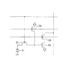
As shown in Figure 3, cmos image sensor has imaging region 10 and peripheral circuit region 20 on a chip.Imaging region 10 comprises pixel array portion, comprising a plurality of pixels of photodiode (photoelectric conversion section) in the two-dimensional directional setting.Peripheral circuit region 20 is arranged on the outside of imaging region 10.
As shown in Figure 4, each pixel 11 of imaging region 10 has pixel transistor, and these transistors comprise photodiode 11, read transistor (transmission grid) 32, amplifier transistor 33, select transistor 34 and reset transistor 35.Photodiode 31 is given birth to signal charge according to the volume production of the light that receives.Read transistor (transmission grid) 32 and read the signal charge of photodiode 31 to FD (diffusion of floating, floating diffusion).Amplifier transistor 33 produces picture element signal according to the electromotive force of FD.Select transistor 34 to select the output time of picture element signal.Reset transistor 35 replacement FD.Each pixel 11 also comprises distribution and other element, with pixel array portion and peripheral circuit region switching signal or power.
Below, will laminated construction according to the cmos image sensor of this embodiment be described referring to figs. 1 to Fig. 2.
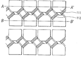
In the drawings, the sensitization part 111 of the photodiode of a plurality of pixels is arranged in the top section of silicon substrate 100.The pixel transistor circuit that is included in each pixel is omitted in Fig. 1 and Fig. 2.Figure 10 illustrates the sensitization part 111 of photodiode and the layout of transmission transistor 112, and transmission transistor 112 is arranged on the corner portions located of sensitization part 111.Schematically illustrated this layout of Figure 10.In fact, transistor is much smaller than the sensitization part, and and such as amplifier transistor, select other transistor of transistor and reset transistor to be provided with together.
Planarization film (interlayer dielectric) 116 and distribution 110 are arranged on the end face of silicon substrate 100 by for example gate insulating film 100A and gate electrode (not shown), and lens 109 are disposed thereon in the layer.As the example in past, lens 109 are convex lens (Figure 12 and Figure 13) in the layer of all each pixels.Lens 109 and distribution 110 are provided with as shown in Figure 9 in the layer.
Planarization film (interlayer dielectric) 115 and distribution 108 are provided with thereon, and lens 107 are provided with thereon in the layer.Lens 107 have structure different with the structure (Figure 12 and Figure 13) of example in the past and the concavees lens for only the pixel with blue filter 104 being provided with in the layer.Lens 107 and distribution 108 are arranged as shown in Figure 8 in the layer.Lenticule 107 forms by following steps: form lens material on whole substrate, according to the lens figure resist on it is patterned into opening shape, form lenticule by carrying out isotropic etching on it on lens material then.Planarization film 115 is formed by SiON basement membrane or low-refraction SiN basement membrane.Lenticule 107 is formed by high index of refraction SiN basement membrane.
Planarization film (interlayer dielectric) 114 and distribution 106 are provided with thereon, and lens 105 are provided with thereon in the layer.Lens 105 have structure different with the structure (Figure 12 and Figure 13) of example in the past and the convex lens for only being provided with for the pixel with red filter 102 in the layer.Lens 105 and orientation 106 are arranged as shown in Figure 7 in the layer.Planarization film 114 is formed by SiON basement membrane or low-refraction SiN basement membrane.Lenticule 105 is formed by high index of refraction SiN basement membrane.
Next, uppermost planarization film 113 is formed thereon, is arranged on the planarization film 113 corresponding to color of pixel filter 102,103 and 104.Fig. 1 illustrates the cross section of the position of red filter 102 and 103 appearance of green filter.Fig. 2 illustrates the cross section of the position of green filter 103 and 104 appearance of blue filter.Color filter 102,103 and 104 is arranged as shown in Figure 6.
The purpose that depends on optimization as the selection of the convex lens of lens or concavees lens in the layer of each color.
As mentioned above, in the imageing sensor according to this embodiment, the number of lens and the structure of lens depend on (comprising lens curvature and/or convex lens or concavees lens) structure of the color filter that the light of each pixel of optimization is collected.The different lenticule structure relevant with the color of color filter can be at the sensitization suboptimization light collection status of color, and it is caused by the difference of wavelength by color filter.This can reduce because the aperture of camera lens and the difference of the angle of light of center and peripheral sensitization part cause center and peripheral sensitization part the unbalanced of the caused colored shadow of collection status of not sharing the same light for color.
The present invention described above is applied to cmos image sensor, but the invention is not restricted to cmos image sensor.The present invention can be applied to have the imageing sensor of a plurality of microlens layers.Optical filter according to the present invention is not limited to the primary colours filter, and can comprise color compensation filter and infrared filter.
Solid state image pickup device is not limited to have the solid state image pickup device of imageing sensor on a chip, and can have such structure, and the imaging moiety that wherein has imageing sensor provides as the package parts that separate with optical system with signal processing.Perhaps, solid state image pickup device is can be with control section and/or operation part integrated and be used as camera system or portable phone.In other words, according to the present invention, the single image transducer can be called solid state image pickup device, and the combination of solid state image pickup device and another funtion part (such as communication module or display module) can be called imaging device.Solid state image pickup device and imaging device comprise within the scope of the invention.
The instantiation of using imaging device of the present invention will be described below.
Figure 11 is the block diagram of structure example that the camera apparatus of the cmos image sensor with embodiment is shown.
In Figure 11, imaging moiety 310 uses example cmos image sensor as shown in Figure 3 and Figure 4 to object image-forming, and output image signal divides 320 to the systems control division on the main substrate.In other words, imaging moiety 310 carries out such as AGC (automatic gain control), OB (optics black) clamper (clamp), CDS (correlated-double-sampling) with to A/D conversion and generation and output digital image signal from the cmos image sensor output signal.
Such example has been described, wherein picture signal is converted to digital signal and is output to systems control division and divides 320 in imaging moiety 310, and analog picture signal can be provided to systems control division from imaging moiety 310 and divide 320 and can divide at systems control division and be converted to digital signal 320.Can use various schemes in the processing in imaging moiety 310 and not be limited to it especially.
Imaging optical system 300 comprises zoom lens 301 and the aperture device 302 that is arranged in the lens tube, and forms subject image in the sensitization part of cmos image sensor.Based on divide 320 instruction under the control of driving/control section 330 from systems control division, corresponding part or a plurality of part are mechanically driven to carry out such as the control of focusing automatically.
Systems control division divides 320 to comprise CPU 321, ROM 322, RAM 323, DSP 324 and external interface 325.
324 pairs of picture signals from imaging moiety 310 of DSP are carried out signal processing to produce the vision signal (such as YUV signal) with the still picture or the mobile picture of predetermined format.
Photographic images can be stored in the storage medium 340 such as storage card, and this storage medium is interchangeable for memory medium controller 341.Storage medium 340 can be disk or the CD media that replaces storage card.
By applying the present invention to camera apparatus, can on various objects, carry out high-quality and take.In this structure, unit component is or/and the combination of unit module can be included in the system, and the size of device can suitably be selected based on commercial actual conditions.Imaging device of the present invention comprises various variations widely.
In solid state image pickup device of the present invention and imaging device, be not limited to people and/or scenery in the general video image by the object of imaging.Solid state image pickup device of the present invention and imaging device also can be applied to the imaging of special precise image figure, such as the imaging in counterfeit money detector or the fingerprint detector.In this situation, replace general camera apparatus shown in Figure 11, the equipment structure also comprises special imaging optical system and comprises the signal processing system of pattern analysis.Also in this situation, operating effect of the present invention can fully be used to realize the exact image detection.
In the remote system that for example telehealth, crime prevention monitoring or individual identify, the equipment structure can comprise the communication module that is connected to aforesaid network, and can obtain various widely application.
It is to be appreciated that those skilled in the art that various modifications, combination, sub-portfolio and variation can carry out according to design needs and other factors, as long as they are in the scope of claim or its equivalent feature.
The present invention comprises and the relevant theme of submitting on October 5th, 2006 in Japan Patent office of Japanese patent application JP2006-274219, it is quoted in full be incorporated into this.
Claims (12)
1. solid state image pickup device comprises:
Semiconductor substrate, it is provided with a plurality of pixels, and each described pixel has photoelectric conversion section;
Multilayer insulating film is layered on the described semiconductor substrate;
Wiring film is arranged between the described multilayer insulating film;
Lens in the layer are for each described photoelectric conversion section is arranged between the described multilayer insulating film;
Optical filter is for each described photoelectric conversion section is arranged on the described dielectric film; And
Lens on the sheet, for each described photoelectric conversion section is arranged on the described optical filter,
Lens have different structures according to the feature of described optical filter for each pixel in the wherein said layer.
2. solid state image pickup device as claimed in claim 1,
Lens are arranged on a plurality of layers between the described multilayer insulating film in the wherein said layer, and
One deck at least of lens is configured to make it partly to form according to the described photoelectric conversion section of the pixel relevant with the part of described optical filter in the wherein said layer.
3. solid state image pickup device as claimed in claim 1, lens comprise convex lens in the wherein said layer.
4. solid state image pickup device as claimed in claim 1, lens comprise concavees lens in the wherein said layer.
5. solid state image pickup device as claimed in claim 1, wherein said optical filter are the primary colours filters.
6. in the solid state image pickup device as claimed in claim 5, wherein said layer on lens and the sheet in the lens at least one color according to described primary colours filter have different structures for each pixel.
7. imaging device comprises:
Solid state image pickup device is to object image-forming;
Imaging optical system forms subject image in the sensitization part of described solid state image pickup device;
Driving/control section drives described imaging optical system;
Signal processing is to carrying out signal processing and produce picture signal from the output signal of described solid state image pickup device;
Recording section, the picture signal that record is produced by described signal processing;
Output, the picture signal that output is produced by described signal processing; And
Operation part, the signal of input control imaging operation;
Wherein said solid state image pickup device comprises:
Semiconductor substrate, it is provided with a plurality of pixels, and each described pixel has photoelectric conversion section;
Multilayer insulating film is layered on the described semiconductor substrate;
Wiring film is arranged between the described multilayer insulating film;
Lens in the layer are for each described photoelectric conversion section is arranged between described a plurality of dielectric film;
Optical filter is for each described photoelectric conversion section is arranged on the described dielectric film; And
Lens on the sheet, for each described photoelectric conversion section is arranged on the described optical filter,
Lens have different structures according to the feature of described optical filter to each pixel in the wherein said layer.
8. imaging device as claimed in claim 7 comprises:
Lens are arranged on a plurality of layers between the described multilayer insulating film in the described layer,
In the wherein said layer lens at least one deck be configured to make it partly to form according to the described photoelectric conversion section of the pixel relevant with the part of described optical filter.
9. imaging device as claimed in claim 7, lens comprise convex lens in the wherein said layer.
10. imaging device as claimed in claim 7, lens comprise concavees lens in the wherein said layer.
11. imaging device as claimed in claim 7, wherein said optical filter are the primary colours filters.
12. in the imaging device as claimed in claim 11, wherein said layer in lens and the sheet lens at least one color according to described primary colours filter have different structures for each pixel.
Applications Claiming Priority (2)
| Application Number | Priority Date | Filing Date | Title |
|---|---|---|---|
| JP274219/06 | 2006-10-05 | ||
| JP2006274219A JP2008091841A (en) | 2006-10-05 | 2006-10-05 | Solid state imaging device and imaging device |
Publications (2)
| Publication Number | Publication Date |
|---|---|
| CN101159281A CN101159281A (en) | 2008-04-09 |
| CN100557810C true CN100557810C (en) | 2009-11-04 |
Family
ID=39307279
Family Applications (1)
| Application Number | Title | Priority Date | Filing Date |
|---|---|---|---|
| CNB200710153178XA Expired - Fee Related CN100557810C (en) | 2006-10-05 | 2007-09-28 | Solid state image pickup device and imaging device |
Country Status (5)
| Country | Link |
|---|---|
| US (1) | US7808542B2 (en) |
| JP (1) | JP2008091841A (en) |
| KR (1) | KR20080031796A (en) |
| CN (1) | CN100557810C (en) |
| TW (1) | TWI357151B (en) |
Families Citing this family (13)
| Publication number | Priority date | Publication date | Assignee | Title |
|---|---|---|---|---|
| JP2010062438A (en) * | 2008-09-05 | 2010-03-18 | Toshiba Corp | Solid-state imaging device and method of designing the same |
| DE102008043992B4 (en) * | 2008-11-21 | 2012-04-05 | Schott Ag | Transparent reactive armor |
| JP5476716B2 (en) * | 2009-01-08 | 2014-04-23 | ソニー株式会社 | Imaging device and imaging apparatus |
| JP5262823B2 (en) | 2009-02-23 | 2013-08-14 | ソニー株式会社 | Solid-state imaging device and electronic apparatus |
| JP5564918B2 (en) | 2009-12-03 | 2014-08-06 | ソニー株式会社 | Image sensor and camera system |
| US10334181B2 (en) | 2012-08-20 | 2019-06-25 | Microsoft Technology Licensing, Llc | Dynamically curved sensor for optical zoom lens |
| WO2014061188A1 (en) * | 2012-10-17 | 2014-04-24 | ソニー株式会社 | Image-capturing element and image-capturing device |
| JP2016015430A (en) * | 2014-07-03 | 2016-01-28 | ソニー株式会社 | Solid-state image sensor and electronic apparatus |
| JP7066316B2 (en) * | 2016-12-13 | 2022-05-13 | ソニーセミコンダクタソリューションズ株式会社 | Image sensor and electronic equipment |
| TWI639022B (en) * | 2017-05-18 | 2018-10-21 | 吳志彥 | Optical element fabrication method and optical sensing device |
| KR102562643B1 (en) * | 2017-07-31 | 2023-08-03 | 제이에스알 가부시끼가이샤 | photoelectric converter |
| TWI772821B (en) * | 2020-06-16 | 2022-08-01 | 大陸商北京集創北方科技股份有限公司 | Full-screen optical image acquisition device and touch display device and handheld device using the same |
| CN113178457B (en) * | 2021-04-12 | 2022-11-11 | 维沃移动通信有限公司 | Pixel structure and image sensor |
Family Cites Families (13)
| Publication number | Priority date | Publication date | Assignee | Title |
|---|---|---|---|---|
| JPS59198754A (en) * | 1983-04-26 | 1984-11-10 | Toshiba Corp | Solid-state color image pickup device |
| JPH10308505A (en) | 1997-03-03 | 1998-11-17 | Toshiba Corp | Solid image pickup device and its applied system |
| JP3620237B2 (en) * | 1997-09-29 | 2005-02-16 | ソニー株式会社 | Solid-state image sensor |
| US6271900B1 (en) * | 1998-03-31 | 2001-08-07 | Intel Corporation | Integrated microlens and color filter structure |
| JP2002151670A (en) | 2000-08-30 | 2002-05-24 | Sony Corp | Solid-state image pickup device and manufacturing method |
| JP2004077530A (en) * | 2002-08-09 | 2004-03-11 | Canon Inc | Focusing method and device |
| JP2004304148A (en) | 2002-09-27 | 2004-10-28 | Sony Corp | Solid state imaging device and manufacturing method therefor |
| US20040105021A1 (en) * | 2002-12-02 | 2004-06-03 | Bolymedia Holdings Co., Ltd. | Color filter patterns for image sensors |
| JP4383959B2 (en) | 2003-05-28 | 2009-12-16 | キヤノン株式会社 | Photoelectric conversion device and manufacturing method thereof |
| JP4546797B2 (en) * | 2004-09-24 | 2010-09-15 | パナソニック株式会社 | Solid-state imaging device, manufacturing method thereof, and camera |
| JP2006120845A (en) | 2004-10-21 | 2006-05-11 | Canon Inc | Photoelectric converter and its manufacturing method |
| JP2006202907A (en) | 2005-01-19 | 2006-08-03 | Canon Inc | Image pickup element |
| JP4512504B2 (en) | 2005-02-24 | 2010-07-28 | 富士フイルム株式会社 | Microlens mounted single-plate color solid-state imaging device and image input device |
-
2006
- 2006-10-05 JP JP2006274219A patent/JP2008091841A/en active Pending
-
2007
- 2007-09-10 TW TW096133709A patent/TWI357151B/en not_active IP Right Cessation
- 2007-09-11 US US11/900,287 patent/US7808542B2/en not_active Expired - Fee Related
- 2007-09-28 CN CNB200710153178XA patent/CN100557810C/en not_active Expired - Fee Related
- 2007-10-04 KR KR1020070099710A patent/KR20080031796A/en not_active Application Discontinuation
Also Published As
| Publication number | Publication date |
|---|---|
| KR20080031796A (en) | 2008-04-11 |
| US7808542B2 (en) | 2010-10-05 |
| US20080174689A1 (en) | 2008-07-24 |
| JP2008091841A (en) | 2008-04-17 |
| TWI357151B (en) | 2012-01-21 |
| CN101159281A (en) | 2008-04-09 |
| TW200832686A (en) | 2008-08-01 |
Similar Documents
| Publication | Publication Date | Title |
|---|---|---|
| CN100557810C (en) | Solid state image pickup device and imaging device | |
| US11916092B2 (en) | Solid-state imaging device, manufacturing method thereof, and electronic apparatus | |
| JP6789820B2 (en) | Solid-state image sensor, its manufacturing method, and electronic equipment | |
| JP3884617B2 (en) | Optoelectronic camera | |
| US8274031B2 (en) | Colored microlens array and manufacturing method for colored microlens array, color solid-state image capturing device and manufacturing method for color solid-state image capturing device, color display apparatus and manufacturing method for color display apparatus, and electronic information device | |
| US7112779B2 (en) | Optical apparatus and beam splitter | |
| JP5180538B2 (en) | Imaging device and imaging apparatus | |
| JP2008005488A (en) | Camera module | |
| CN104681572A (en) | Solid-state imaging device and electronic apparatus | |
| JP3478796B2 (en) | Solid-state imaging device | |
| JP2013046013A (en) | Solid-state imaging device and electronic apparatus | |
| WO2012133551A1 (en) | Method for driving solid-state imaging element, solid-state imaging element, and imaging device | |
| US7355154B2 (en) | Image sensing apparatus with movable light flux splitter and control method thereof | |
| JP4512504B2 (en) | Microlens mounted single-plate color solid-state imaging device and image input device | |
| JP2006126652A (en) | Imaging apparatus | |
| JP5532766B2 (en) | Imaging device and imaging apparatus | |
| JP2010093490A (en) | Image pickup apparatus | |
| JP5176453B2 (en) | Solid-state imaging device, method for manufacturing solid-state imaging device, and imaging device | |
| JP4564794B2 (en) | Solid-state image sensor | |
| JP2009004605A (en) | Image sensor and imaging device | |
| JP2009188461A (en) | Imaging apparatus | |
| JP5018125B2 (en) | Solid-state imaging device and imaging device | |
| JP2008235753A (en) | Solid imaging apparatus and method of manufacturing the same | |
| JP2005175893A (en) | Two-plate type color solid-state image pickup device and digital camera | |
| JP2005259750A (en) | Multiple-disk color solid state imaging device and digital camera |
Legal Events
| Date | Code | Title | Description |
|---|---|---|---|
| C06 | Publication | ||
| PB01 | Publication | ||
| C10 | Entry into substantive examination | ||
| SE01 | Entry into force of request for substantive examination | ||
| C14 | Grant of patent or utility model | ||
| GR01 | Patent grant | ||
| C17 | Cessation of patent right | ||
| CF01 | Termination of patent right due to non-payment of annual fee |
Granted publication date: 20091104 Termination date: 20130928 |