CN100514591C - A method of manufacturing semiconductor packages and packages made - Google Patents
A method of manufacturing semiconductor packages and packages made Download PDFInfo
- Publication number
- CN100514591C CN100514591C CNB2006800064736A CN200680006473A CN100514591C CN 100514591 C CN100514591 C CN 100514591C CN B2006800064736 A CNB2006800064736 A CN B2006800064736A CN 200680006473 A CN200680006473 A CN 200680006473A CN 100514591 C CN100514591 C CN 100514591C
- Authority
- CN
- China
- Prior art keywords
- resin bed
- encapsulation
- passivation layer
- semiconductor
- contact
- Prior art date
- Legal status (The legal status is an assumption and is not a legal conclusion. Google has not performed a legal analysis and makes no representation as to the accuracy of the status listed.)
- Expired - Fee Related
Links
Images


Classifications
-
- H—ELECTRICITY
- H01—ELECTRIC ELEMENTS
- H01L—SEMICONDUCTOR DEVICES NOT COVERED BY CLASS H10
- H01L23/00—Details of semiconductor or other solid state devices
- H01L23/52—Arrangements for conducting electric current within the device in operation from one component to another, i.e. interconnections, e.g. wires, lead frames
- H01L23/538—Arrangements for conducting electric current within the device in operation from one component to another, i.e. interconnections, e.g. wires, lead frames the interconnection structure between a plurality of semiconductor chips being formed on, or in, insulating substrates
- H01L23/5389—Arrangements for conducting electric current within the device in operation from one component to another, i.e. interconnections, e.g. wires, lead frames the interconnection structure between a plurality of semiconductor chips being formed on, or in, insulating substrates the chips being integrally enclosed by the interconnect and support structures
-
- H—ELECTRICITY
- H01—ELECTRIC ELEMENTS
- H01L—SEMICONDUCTOR DEVICES NOT COVERED BY CLASS H10
- H01L21/00—Processes or apparatus adapted for the manufacture or treatment of semiconductor or solid state devices or of parts thereof
- H01L21/67—Apparatus specially adapted for handling semiconductor or electric solid state devices during manufacture or treatment thereof; Apparatus specially adapted for handling wafers during manufacture or treatment of semiconductor or electric solid state devices or components ; Apparatus not specifically provided for elsewhere
- H01L21/683—Apparatus specially adapted for handling semiconductor or electric solid state devices during manufacture or treatment thereof; Apparatus specially adapted for handling wafers during manufacture or treatment of semiconductor or electric solid state devices or components ; Apparatus not specifically provided for elsewhere for supporting or gripping
- H01L21/6835—Apparatus specially adapted for handling semiconductor or electric solid state devices during manufacture or treatment thereof; Apparatus specially adapted for handling wafers during manufacture or treatment of semiconductor or electric solid state devices or components ; Apparatus not specifically provided for elsewhere for supporting or gripping using temporarily an auxiliary support
-
- H—ELECTRICITY
- H01—ELECTRIC ELEMENTS
- H01L—SEMICONDUCTOR DEVICES NOT COVERED BY CLASS H10
- H01L24/00—Arrangements for connecting or disconnecting semiconductor or solid-state bodies; Methods or apparatus related thereto
- H01L24/01—Means for bonding being attached to, or being formed on, the surface to be connected, e.g. chip-to-package, die-attach, "first-level" interconnects; Manufacturing methods related thereto
- H01L24/18—High density interconnect [HDI] connectors; Manufacturing methods related thereto
- H01L24/23—Structure, shape, material or disposition of the high density interconnect connectors after the connecting process
- H01L24/24—Structure, shape, material or disposition of the high density interconnect connectors after the connecting process of an individual high density interconnect connector
-
- H—ELECTRICITY
- H01—ELECTRIC ELEMENTS
- H01L—SEMICONDUCTOR DEVICES NOT COVERED BY CLASS H10
- H01L24/00—Arrangements for connecting or disconnecting semiconductor or solid-state bodies; Methods or apparatus related thereto
- H01L24/80—Methods for connecting semiconductor or other solid state bodies using means for bonding being attached to, or being formed on, the surface to be connected
- H01L24/82—Methods for connecting semiconductor or other solid state bodies using means for bonding being attached to, or being formed on, the surface to be connected by forming build-up interconnects at chip-level, e.g. for high density interconnects [HDI]
-
- H—ELECTRICITY
- H01—ELECTRIC ELEMENTS
- H01L—SEMICONDUCTOR DEVICES NOT COVERED BY CLASS H10
- H01L24/00—Arrangements for connecting or disconnecting semiconductor or solid-state bodies; Methods or apparatus related thereto
- H01L24/93—Batch processes
- H01L24/95—Batch processes at chip-level, i.e. with connecting carried out on a plurality of singulated devices, i.e. on diced chips
- H01L24/97—Batch processes at chip-level, i.e. with connecting carried out on a plurality of singulated devices, i.e. on diced chips the devices being connected to a common substrate, e.g. interposer, said common substrate being separable into individual assemblies after connecting
-
- H—ELECTRICITY
- H01—ELECTRIC ELEMENTS
- H01L—SEMICONDUCTOR DEVICES NOT COVERED BY CLASS H10
- H01L2221/00—Processes or apparatus adapted for the manufacture or treatment of semiconductor or solid state devices or of parts thereof covered by H01L21/00
- H01L2221/67—Apparatus for handling semiconductor or electric solid state devices during manufacture or treatment thereof; Apparatus for handling wafers during manufacture or treatment of semiconductor or electric solid state devices or components; Apparatus not specifically provided for elsewhere
- H01L2221/683—Apparatus for handling semiconductor or electric solid state devices during manufacture or treatment thereof; Apparatus for handling wafers during manufacture or treatment of semiconductor or electric solid state devices or components; Apparatus not specifically provided for elsewhere for supporting or gripping
- H01L2221/68304—Apparatus for handling semiconductor or electric solid state devices during manufacture or treatment thereof; Apparatus for handling wafers during manufacture or treatment of semiconductor or electric solid state devices or components; Apparatus not specifically provided for elsewhere for supporting or gripping using temporarily an auxiliary support
- H01L2221/68327—Apparatus for handling semiconductor or electric solid state devices during manufacture or treatment thereof; Apparatus for handling wafers during manufacture or treatment of semiconductor or electric solid state devices or components; Apparatus not specifically provided for elsewhere for supporting or gripping using temporarily an auxiliary support used during dicing or grinding
- H01L2221/68331—Apparatus for handling semiconductor or electric solid state devices during manufacture or treatment thereof; Apparatus for handling wafers during manufacture or treatment of semiconductor or electric solid state devices or components; Apparatus not specifically provided for elsewhere for supporting or gripping using temporarily an auxiliary support used during dicing or grinding of passive members, e.g. die mounting substrate
-
- H—ELECTRICITY
- H01—ELECTRIC ELEMENTS
- H01L—SEMICONDUCTOR DEVICES NOT COVERED BY CLASS H10
- H01L2221/00—Processes or apparatus adapted for the manufacture or treatment of semiconductor or solid state devices or of parts thereof covered by H01L21/00
- H01L2221/67—Apparatus for handling semiconductor or electric solid state devices during manufacture or treatment thereof; Apparatus for handling wafers during manufacture or treatment of semiconductor or electric solid state devices or components; Apparatus not specifically provided for elsewhere
- H01L2221/683—Apparatus for handling semiconductor or electric solid state devices during manufacture or treatment thereof; Apparatus for handling wafers during manufacture or treatment of semiconductor or electric solid state devices or components; Apparatus not specifically provided for elsewhere for supporting or gripping
- H01L2221/68304—Apparatus for handling semiconductor or electric solid state devices during manufacture or treatment thereof; Apparatus for handling wafers during manufacture or treatment of semiconductor or electric solid state devices or components; Apparatus not specifically provided for elsewhere for supporting or gripping using temporarily an auxiliary support
- H01L2221/68345—Apparatus for handling semiconductor or electric solid state devices during manufacture or treatment thereof; Apparatus for handling wafers during manufacture or treatment of semiconductor or electric solid state devices or components; Apparatus not specifically provided for elsewhere for supporting or gripping using temporarily an auxiliary support used as a support during the manufacture of self supporting substrates
-
- H—ELECTRICITY
- H01—ELECTRIC ELEMENTS
- H01L—SEMICONDUCTOR DEVICES NOT COVERED BY CLASS H10
- H01L2221/00—Processes or apparatus adapted for the manufacture or treatment of semiconductor or solid state devices or of parts thereof covered by H01L21/00
- H01L2221/67—Apparatus for handling semiconductor or electric solid state devices during manufacture or treatment thereof; Apparatus for handling wafers during manufacture or treatment of semiconductor or electric solid state devices or components; Apparatus not specifically provided for elsewhere
- H01L2221/683—Apparatus for handling semiconductor or electric solid state devices during manufacture or treatment thereof; Apparatus for handling wafers during manufacture or treatment of semiconductor or electric solid state devices or components; Apparatus not specifically provided for elsewhere for supporting or gripping
- H01L2221/68304—Apparatus for handling semiconductor or electric solid state devices during manufacture or treatment thereof; Apparatus for handling wafers during manufacture or treatment of semiconductor or electric solid state devices or components; Apparatus not specifically provided for elsewhere for supporting or gripping using temporarily an auxiliary support
- H01L2221/68368—Apparatus for handling semiconductor or electric solid state devices during manufacture or treatment thereof; Apparatus for handling wafers during manufacture or treatment of semiconductor or electric solid state devices or components; Apparatus not specifically provided for elsewhere for supporting or gripping using temporarily an auxiliary support used in a transfer process involving at least two transfer steps, i.e. including an intermediate handle substrate
-
- H—ELECTRICITY
- H01—ELECTRIC ELEMENTS
- H01L—SEMICONDUCTOR DEVICES NOT COVERED BY CLASS H10
- H01L2223/00—Details relating to semiconductor or other solid state devices covered by the group H01L23/00
- H01L2223/58—Structural electrical arrangements for semiconductor devices not otherwise provided for
- H01L2223/64—Impedance arrangements
- H01L2223/66—High-frequency adaptations
- H01L2223/6661—High-frequency adaptations for passive devices
- H01L2223/6677—High-frequency adaptations for passive devices for antenna, e.g. antenna included within housing of semiconductor device
-
- H—ELECTRICITY
- H01—ELECTRIC ELEMENTS
- H01L—SEMICONDUCTOR DEVICES NOT COVERED BY CLASS H10
- H01L2224/00—Indexing scheme for arrangements for connecting or disconnecting semiconductor or solid-state bodies and methods related thereto as covered by H01L24/00
- H01L2224/01—Means for bonding being attached to, or being formed on, the surface to be connected, e.g. chip-to-package, die-attach, "first-level" interconnects; Manufacturing methods related thereto
- H01L2224/18—High density interconnect [HDI] connectors; Manufacturing methods related thereto
- H01L2224/23—Structure, shape, material or disposition of the high density interconnect connectors after the connecting process
- H01L2224/24—Structure, shape, material or disposition of the high density interconnect connectors after the connecting process of an individual high density interconnect connector
- H01L2224/241—Disposition
- H01L2224/24151—Connecting between a semiconductor or solid-state body and an item not being a semiconductor or solid-state body, e.g. chip-to-substrate, chip-to-passive
- H01L2224/24221—Connecting between a semiconductor or solid-state body and an item not being a semiconductor or solid-state body, e.g. chip-to-substrate, chip-to-passive the body and the item being stacked
- H01L2224/24225—Connecting between a semiconductor or solid-state body and an item not being a semiconductor or solid-state body, e.g. chip-to-substrate, chip-to-passive the body and the item being stacked the item being non-metallic, e.g. insulating substrate with or without metallisation
- H01L2224/24226—Connecting between a semiconductor or solid-state body and an item not being a semiconductor or solid-state body, e.g. chip-to-substrate, chip-to-passive the body and the item being stacked the item being non-metallic, e.g. insulating substrate with or without metallisation the HDI interconnect connecting to the same level of the item at which the semiconductor or solid-state body is mounted, e.g. the item being planar
-
- H—ELECTRICITY
- H01—ELECTRIC ELEMENTS
- H01L—SEMICONDUCTOR DEVICES NOT COVERED BY CLASS H10
- H01L2224/00—Indexing scheme for arrangements for connecting or disconnecting semiconductor or solid-state bodies and methods related thereto as covered by H01L24/00
- H01L2224/93—Batch processes
- H01L2224/95—Batch processes at chip-level, i.e. with connecting carried out on a plurality of singulated devices, i.e. on diced chips
- H01L2224/97—Batch processes at chip-level, i.e. with connecting carried out on a plurality of singulated devices, i.e. on diced chips the devices being connected to a common substrate, e.g. interposer, said common substrate being separable into individual assemblies after connecting
-
- H—ELECTRICITY
- H01—ELECTRIC ELEMENTS
- H01L—SEMICONDUCTOR DEVICES NOT COVERED BY CLASS H10
- H01L2924/00—Indexing scheme for arrangements or methods for connecting or disconnecting semiconductor or solid-state bodies as covered by H01L24/00
- H01L2924/01—Chemical elements
- H01L2924/01005—Boron [B]
-
- H—ELECTRICITY
- H01—ELECTRIC ELEMENTS
- H01L—SEMICONDUCTOR DEVICES NOT COVERED BY CLASS H10
- H01L2924/00—Indexing scheme for arrangements or methods for connecting or disconnecting semiconductor or solid-state bodies as covered by H01L24/00
- H01L2924/01—Chemical elements
- H01L2924/01006—Carbon [C]
-
- H—ELECTRICITY
- H01—ELECTRIC ELEMENTS
- H01L—SEMICONDUCTOR DEVICES NOT COVERED BY CLASS H10
- H01L2924/00—Indexing scheme for arrangements or methods for connecting or disconnecting semiconductor or solid-state bodies as covered by H01L24/00
- H01L2924/01—Chemical elements
- H01L2924/01013—Aluminum [Al]
-
- H—ELECTRICITY
- H01—ELECTRIC ELEMENTS
- H01L—SEMICONDUCTOR DEVICES NOT COVERED BY CLASS H10
- H01L2924/00—Indexing scheme for arrangements or methods for connecting or disconnecting semiconductor or solid-state bodies as covered by H01L24/00
- H01L2924/01—Chemical elements
- H01L2924/01015—Phosphorus [P]
-
- H—ELECTRICITY
- H01—ELECTRIC ELEMENTS
- H01L—SEMICONDUCTOR DEVICES NOT COVERED BY CLASS H10
- H01L2924/00—Indexing scheme for arrangements or methods for connecting or disconnecting semiconductor or solid-state bodies as covered by H01L24/00
- H01L2924/01—Chemical elements
- H01L2924/01023—Vanadium [V]
-
- H—ELECTRICITY
- H01—ELECTRIC ELEMENTS
- H01L—SEMICONDUCTOR DEVICES NOT COVERED BY CLASS H10
- H01L2924/00—Indexing scheme for arrangements or methods for connecting or disconnecting semiconductor or solid-state bodies as covered by H01L24/00
- H01L2924/01—Chemical elements
- H01L2924/01029—Copper [Cu]
-
- H—ELECTRICITY
- H01—ELECTRIC ELEMENTS
- H01L—SEMICONDUCTOR DEVICES NOT COVERED BY CLASS H10
- H01L2924/00—Indexing scheme for arrangements or methods for connecting or disconnecting semiconductor or solid-state bodies as covered by H01L24/00
- H01L2924/01—Chemical elements
- H01L2924/0103—Zinc [Zn]
-
- H—ELECTRICITY
- H01—ELECTRIC ELEMENTS
- H01L—SEMICONDUCTOR DEVICES NOT COVERED BY CLASS H10
- H01L2924/00—Indexing scheme for arrangements or methods for connecting or disconnecting semiconductor or solid-state bodies as covered by H01L24/00
- H01L2924/01—Chemical elements
- H01L2924/01033—Arsenic [As]
-
- H—ELECTRICITY
- H01—ELECTRIC ELEMENTS
- H01L—SEMICONDUCTOR DEVICES NOT COVERED BY CLASS H10
- H01L2924/00—Indexing scheme for arrangements or methods for connecting or disconnecting semiconductor or solid-state bodies as covered by H01L24/00
- H01L2924/01—Chemical elements
- H01L2924/01047—Silver [Ag]
-
- H—ELECTRICITY
- H01—ELECTRIC ELEMENTS
- H01L—SEMICONDUCTOR DEVICES NOT COVERED BY CLASS H10
- H01L2924/00—Indexing scheme for arrangements or methods for connecting or disconnecting semiconductor or solid-state bodies as covered by H01L24/00
- H01L2924/01—Chemical elements
- H01L2924/01078—Platinum [Pt]
-
- H—ELECTRICITY
- H01—ELECTRIC ELEMENTS
- H01L—SEMICONDUCTOR DEVICES NOT COVERED BY CLASS H10
- H01L2924/00—Indexing scheme for arrangements or methods for connecting or disconnecting semiconductor or solid-state bodies as covered by H01L24/00
- H01L2924/01—Chemical elements
- H01L2924/01079—Gold [Au]
-
- H—ELECTRICITY
- H01—ELECTRIC ELEMENTS
- H01L—SEMICONDUCTOR DEVICES NOT COVERED BY CLASS H10
- H01L2924/00—Indexing scheme for arrangements or methods for connecting or disconnecting semiconductor or solid-state bodies as covered by H01L24/00
- H01L2924/01—Chemical elements
- H01L2924/01082—Lead [Pb]
-
- H—ELECTRICITY
- H01—ELECTRIC ELEMENTS
- H01L—SEMICONDUCTOR DEVICES NOT COVERED BY CLASS H10
- H01L2924/00—Indexing scheme for arrangements or methods for connecting or disconnecting semiconductor or solid-state bodies as covered by H01L24/00
- H01L2924/013—Alloys
- H01L2924/0132—Binary Alloys
- H01L2924/01327—Intermediate phases, i.e. intermetallics compounds
-
- H—ELECTRICITY
- H01—ELECTRIC ELEMENTS
- H01L—SEMICONDUCTOR DEVICES NOT COVERED BY CLASS H10
- H01L2924/00—Indexing scheme for arrangements or methods for connecting or disconnecting semiconductor or solid-state bodies as covered by H01L24/00
- H01L2924/013—Alloys
- H01L2924/014—Solder alloys
-
- H—ELECTRICITY
- H01—ELECTRIC ELEMENTS
- H01L—SEMICONDUCTOR DEVICES NOT COVERED BY CLASS H10
- H01L2924/00—Indexing scheme for arrangements or methods for connecting or disconnecting semiconductor or solid-state bodies as covered by H01L24/00
- H01L2924/10—Details of semiconductor or other solid state devices to be connected
- H01L2924/102—Material of the semiconductor or solid state bodies
- H01L2924/1025—Semiconducting materials
- H01L2924/1026—Compound semiconductors
- H01L2924/1032—III-V
- H01L2924/10329—Gallium arsenide [GaAs]
-
- H—ELECTRICITY
- H01—ELECTRIC ELEMENTS
- H01L—SEMICONDUCTOR DEVICES NOT COVERED BY CLASS H10
- H01L2924/00—Indexing scheme for arrangements or methods for connecting or disconnecting semiconductor or solid-state bodies as covered by H01L24/00
- H01L2924/10—Details of semiconductor or other solid state devices to be connected
- H01L2924/11—Device type
- H01L2924/12—Passive devices, e.g. 2 terminal devices
- H01L2924/1204—Optical Diode
- H01L2924/12041—LED
-
- H—ELECTRICITY
- H01—ELECTRIC ELEMENTS
- H01L—SEMICONDUCTOR DEVICES NOT COVERED BY CLASS H10
- H01L2924/00—Indexing scheme for arrangements or methods for connecting or disconnecting semiconductor or solid-state bodies as covered by H01L24/00
- H01L2924/10—Details of semiconductor or other solid state devices to be connected
- H01L2924/11—Device type
- H01L2924/12—Passive devices, e.g. 2 terminal devices
- H01L2924/1204—Optical Diode
- H01L2924/12042—LASER
-
- H—ELECTRICITY
- H01—ELECTRIC ELEMENTS
- H01L—SEMICONDUCTOR DEVICES NOT COVERED BY CLASS H10
- H01L2924/00—Indexing scheme for arrangements or methods for connecting or disconnecting semiconductor or solid-state bodies as covered by H01L24/00
- H01L2924/10—Details of semiconductor or other solid state devices to be connected
- H01L2924/11—Device type
- H01L2924/14—Integrated circuits
-
- H—ELECTRICITY
- H01—ELECTRIC ELEMENTS
- H01L—SEMICONDUCTOR DEVICES NOT COVERED BY CLASS H10
- H01L2924/00—Indexing scheme for arrangements or methods for connecting or disconnecting semiconductor or solid-state bodies as covered by H01L24/00
- H01L2924/15—Details of package parts other than the semiconductor or other solid state devices to be connected
- H01L2924/151—Die mounting substrate
- H01L2924/153—Connection portion
- H01L2924/1531—Connection portion the connection portion being formed only on the surface of the substrate opposite to the die mounting surface
- H01L2924/15311—Connection portion the connection portion being formed only on the surface of the substrate opposite to the die mounting surface being a ball array, e.g. BGA
-
- H—ELECTRICITY
- H01—ELECTRIC ELEMENTS
- H01L—SEMICONDUCTOR DEVICES NOT COVERED BY CLASS H10
- H01L2924/00—Indexing scheme for arrangements or methods for connecting or disconnecting semiconductor or solid-state bodies as covered by H01L24/00
- H01L2924/15—Details of package parts other than the semiconductor or other solid state devices to be connected
- H01L2924/151—Die mounting substrate
- H01L2924/153—Connection portion
- H01L2924/1532—Connection portion the connection portion being formed on the die mounting surface of the substrate
- H01L2924/1533—Connection portion the connection portion being formed on the die mounting surface of the substrate the connection portion being formed both on the die mounting surface of the substrate and outside the die mounting surface of the substrate
- H01L2924/15331—Connection portion the connection portion being formed on the die mounting surface of the substrate the connection portion being formed both on the die mounting surface of the substrate and outside the die mounting surface of the substrate being a ball array, e.g. BGA
-
- H—ELECTRICITY
- H01—ELECTRIC ELEMENTS
- H01L—SEMICONDUCTOR DEVICES NOT COVERED BY CLASS H10
- H01L2924/00—Indexing scheme for arrangements or methods for connecting or disconnecting semiconductor or solid-state bodies as covered by H01L24/00
- H01L2924/19—Details of hybrid assemblies other than the semiconductor or other solid state devices to be connected
- H01L2924/1901—Structure
- H01L2924/1904—Component type
- H01L2924/19041—Component type being a capacitor
-
- H—ELECTRICITY
- H01—ELECTRIC ELEMENTS
- H01L—SEMICONDUCTOR DEVICES NOT COVERED BY CLASS H10
- H01L2924/00—Indexing scheme for arrangements or methods for connecting or disconnecting semiconductor or solid-state bodies as covered by H01L24/00
- H01L2924/19—Details of hybrid assemblies other than the semiconductor or other solid state devices to be connected
- H01L2924/1901—Structure
- H01L2924/1904—Component type
- H01L2924/19042—Component type being an inductor
Abstract
The flexible package (100) has between a first (1) and a second side (2) a semiconductor device (20) with a thinned back substrate (10) and an interconnect structure. Contact means (31,33) for external contact and a first resin layer (52) are present at the first side (2) of the package (100), which contact means (31,33) are coupled to the interconnect structure. At the second side (2) the semiconductor device (20) is at least substantially covered with a second resin layer (12). The contact means (31,33) are present on the first resin layer (52) and are coupled to the interconnect structure with redistribution tracks (32,34) extending through the first resin layer (52). A passivation layer (55) covers the first resin layer (52) and the redistribution tracks (32,34) at least substantially.
Description
Technical field
The present invention relates to a kind of flexible semiconductor encapsulation with first and second, between its two sides, exist and have the back substrate of attenuate and the semiconductor device of interconnection structure, on its first, there be the contact device and first resin bed that is used for outside contact, described contact device is coupled to interconnection structure, and locating semiconductor device at described second is covered by second resin bed at least basically, wherein contact device is present on first resin bed and utilizes the redistribution path that extends in the hole of passing first resin bed to be coupled to interconnection structure, and passivation layer covers first resin bed and redistribution path at least basically.
The invention still further relates to the method for making a plurality of semiconductor packages, comprise the steps:
One provides a kind of wafer, and it has real estate with relative interconnection face and have a plurality of semiconductor device, and described a plurality of semiconductor device have interconnection structure at this interconnect mask;
-coated with resins layer on interconnection structure;
-utilize adhesive that wafer first face is attached on the carrier;
-from second attenuate silicon chip;
-another resin bed of coating on second of wafer; And
-remove at least some formed like this semiconductor packages from carrier,
Wherein contact device is defined on first resin bed, utilizes the redistribution path that extends through the hole in this first resin bed that described contact device is coupled to interconnection structure, and passivation layer is coated on this first resin bed and the redistribution path.
Technical background
EP1418617 relates to the manufacture method of semiconductor device, it comprises the steps: to prepare the circuit board that has wiring pattern on a surface, the binding post of electronic chip is bonded to the wiring pattern of circuit board by the flip-chip bonding, wherein this electronic chip has predetermined element and this binding post on a surface, on circuit board, form and have the dielectric film of another surperficial thickness at least that exposes electronic chip, and described another surface by grinding electronic chip and the dielectric film thickness that reduces electronic chip.
This method and this device be from US-B 6,753, and 238 know.In this known method, projection is applied on the interconnection structure that exposes by the contact hole that passes passivating film.The projection that applies thereon has 20 to 40 microns height, and any space between the projection all is full of for example thermosetting resin of epoxy resin etc.It is made as same thickness so that have flat surfaces.Utilize then the thermocompression bonding method with adhesive with wafer bonding to carrier.This carrier is a porous aluminum hydrochlorate plate.In order to remove this plate, wafer is immersed in the high temperature organic solution groove, so that dissolve this adhesive.Can apply second resin bed with the thickness identical with first resin bed.Perhaps, can use ultraviolet ray to shine transparent carrier, can peel off this semiconductor packages from adhesive then.
This well-known device, especially for extremely thin encapsulation, shortcoming is that it is easy to form the crack.
Summary of the invention
Therefore first purpose of the present invention provides a kind of encapsulation of the type of being mentioned in introductory song, and its risk that forms the crack has reduced.
Wherein realized this purpose in the following manner, the hole of promptly feasible this first resin bed of redistribution path underfill.Suitably, cover this second resin bed with passivation layer.Being easy to of well-known device forms the weakness in crack and particularly utilizes the difference of the thermal expansion between the projection printed circuit board (PCB) attached to it caused by encapsulation and its.Therefore these projections are most important for compensating action.Yet they highly are integrated in the known encapsulation, thereby thereby any stress are sent to interconnection structure and sends device to from projection.Yet this rigid element of encapsulation is the most susceptible part.In structure of the present invention, resin bed is effective as stressed barrier, and it can reduce by the caused stress of the difference of thermal expansion.
Contact device in the device of the present invention is preferably contact pad, can apply solder projection or metal or conducting resinl on it.Yet not getting rid of contact device is the antenna that is used for the noncontact coupling, such as coil, ambipolar (dipolar) antenna or even condenser armature.
In addition, combine the existence of the contact device on the resin bed top, the result shows needs application passivation layer.It has some functions.At first, this passivation layer is as solder mask.Secondly, this passivation layer protection redistribution path.Consider the thickness of the resin bed of several micron dimensions, hole wherein has the shape of the cone of approximate upset, perhaps is seen as U-shaped or V-arrangement from the cross section.This causes redistributing on the sidewall that path exists only in cone, and it is not full of.The coupling of considering thermal coefficient of expansion is comparatively inessential, and this underfill is suitable.Yet, especially for flexible encapsulation, described hole may develop into machinery or chemical aspect weak spot, may begin to produce crack or pollutant at this place may enter encapsulation at this place.The passivation layer that extends on these paths forms continuous thin slice, and chemistry and two kinds of protections of machinery are provided thus.
The encapsulation itself that has the redistribution path on the top of resin bed is from US6, and 506,664, especially know in Fig. 7 and the wherein relevant explanation.Yet this well-known device is not present between first and second resin beds, makes this well-known device be under the compression strain.This shows the formation that is necessary to prevent the crack in the process of separating technology and bending.Consider the part of encapsulation as lamination, it demonstrates resulting lamination and does not have the flexible of height, and therefore has other mechanical properties that are different from flexible encapsulation of the present invention.This known encapsulation comprises the perpendicular interconnection that is full of by resin bed, and does not have passivation layer, and this is tangible.
The encapsulation of type of the present invention, in pre-published application PCT/IB 2004/0516 (PHNL031150), be further described.Yet, unexposed oxide layer on the resin bed is carried out composition so that expose contact pad at this, and unexposed its can be used as passivation layer.In addition, unexposed passivation layer can be oxynitride or nitride, and it is favourable to passivation properties.
In a preferred embodiment, second resin bed also is coated with passivation layer.Second face also can suitably be provided with contact pad, and this is especially preferred.For example, the encapsulation that this generation can be stacked.Another selection is that inductor, (another) antenna or capacitor are provided on second resin bed.Yet, do not exist under the situation of any conductive trajectory on second resin bed, it also is favourable having passivation layer.Especially, passivation layer makes resin bed avoid contacting binding agent.Therefore, the encapsulation with attenuate becomes more or less freely from carrier release.
In one embodiment, semiconductor device is provided with real estate and interconnection face, have semiconductor substrate and have interconnection structure at this interconnection face at this real estate, and wherein said first resin bed is present on the real estate and described second resin is present on the interconnection face.Yet in the prior art, projection is present on the interconnection face of device, and structure of the present invention allows to be used to provide projection with the substrate-side of device.This advantage that has is to need not to cover projection with adhesive layer in manufacture process.The existence of projection needs thicker adhesive layer and needs the follow-up cleaning to projection.Adhesive layer is attached to encapsulation in the temporary transient carrier that is generally glass plate.In the thinning process of semiconductor substrate, need this temporary transient carrier to be used to keep the needs of stability.
Suitably, resin bed is the material that glass transformation temperature is higher than the fusion temperature of scolder.For lead-free solder, this fusion temperature is approximately 270 ℃.
Especially the material of Shi Heing is epoxy resin and polyimides.Polyimides is the polymer resin that comprises aryl and acid imide.The example of polyimide polymer is polyimides, poly-different acid imide, maleimide, bismaleimides, polyamidoimide, polymidimides, Polyetherimide and polyimides-iso-indoles quinazoline diones acid imide.
Suitably, passivation layer comprises inorganic material.Chemical vapour deposition (CVD) and especially plasma enhanced chemical vapor deposition (PECVD) are regarded as effectively and are used to provide that subsurface material is had the good passivation layer that adheres to.In addition, the PECVD technology allows to deposit under the temperature of the glass transformation temperature that is lower than resin.Only material is silica, silicon oxynitride and silicon nitride.
Inorganic passivation layer is particularly useful when combining with polyimide resin.A shortcoming of polyimides is that they are relatively poor relatively to adhering to of metal.Inorganic passivation layer of the present invention has relatively preferably polyimides and adheres to.The hole of inorganic passivation layer is provided, makes that only part exposes redistribution path and contact pad.Thereby contact pad is clipped between resin bed and the passivation layer in their edge.This fixes metal effectively.Thereby, improved the stability of whole encapsulation fully.
In another embodiment, semiconductor device is provided with the substrate with insulating barrier, and extends up to insulating barrier in hole in the close corresponding resin bed of passivation layer and/or the hole in corresponding resin bed, thereby forms the shell of the sealing of semiconductor device.Many have the resin bed deficiency of suitable elastic characteristic so that semiconductor device is avoided pollutant and/or moisture.For the polyimides that is easy to absorb water especially like this.The closure that passivation layer has been arranged has been protected device fully.Insulating barrier in the substrate can be the layer that is buried at first in the substrate.Yet it also can be top layer that is provided as substrate and the thermal oxide layer (LOCOS) that is known in the art usually.
Advantageously, one of resin bed extends to the transverse side of encapsulation.Suitably, second resin bed is carried out composition, with definition split tunnel (lane).This is favourable, because it allows to remove any substrate portion or ceramic layer in the split tunnel under etched help.If this removal utilizes sawing to implement, the saw that then passes some materials causes the extra stress of introducing in encapsulation.In order to make encapsulation stable and mechanically and chemically protection packaging, find that second passivation layer is useful.
In a relevant therewith favourable modification, described resin bed has the edge of rounding (rounded).Provide this rounded edges at an easy rate, because in etch processes or for example in the optics ablation processes of laser ablation etc. resin bed is carried out composition.The existence of rounded edges prevents the generation in the crack of edge.Especially preferred is to pass first resin bed by sawing or cutting will encapsulate separated from one another.This causes the first resin bed horizontal expansion to surpass second resin bed.
In another modification, at least one contact pad is present on second resin bed and by the hole in the passivation layer and comes out.Provide one or more contact pads to the composition of second resin bed and second face that makes it possible in encapsulation that provides of second passivation layer, and need not too many extra processing.On second, provide contact pad to allow to pile up in simple mode.In addition, encapsulate self and can perhaps offer any surface of the suitable contact of having of electronic device as the carrier of further IC as label.
Encapsulation of the present invention can suitably be used as the lamination of the encapsulation with a plurality of devices.For this situation, all encapsulation in the lamination need not to have same size.
Encapsulation of the present invention can also be as the label of flexible devices.It can be used as and can curl or the display driver of flexible display.It can be used for the security purpose of safety paper, especially by being applied to safety line or other band.It can especially be used for identification in human body in medical application.
Second purpose of the present invention is the manufacture method that a kind of type of mentioning at introductory song is provided for device of the present invention.
This purpose is realized in the hole that is not full of first resin bed by the redistribution path.
Method of the present invention has produced device of the present invention and can be used for many interesting embodiment.
The redistribution path that preferably will extend through first resin bed is limited in one deck.Preferably contact pad is limited in this identical layer.Yet, can use path and the path on first resin bed in principle respectively by first resin bed.
Passivation layer suitably comprises inorganic material.Favourable deposition technique is for producing fine and close layer and low pressure and the plasma enhanced chemical vapor deposition of carrying out under the temperature that reduces.Do not get rid of passivation layer and comprise some sublayers.
The exposure of contact pad is not got rid of passivation layer and is partly covered contact pad, so it is " solder resist limit (resist defined) ".Contact pad that should " solder resist qualification " even be particularly useful for the appropriate functional of passivation layer.
By using suitable material, especially metal or alloy, contact pad is suitably thickened.The optimum nickel that is to use.This metal can be used in this electroless plating techniques known as the technical staff.
The form that is applied to scolder on the contact pad and is solder caps (solder cap) is favourable.In the application's context, term " solder caps " refers to that solder dots and following laminar surface impale one less than 90 ° angle.This solder caps is favourable for the use in intrinsic thin encapsulation of the present invention, because described cap also has limited height.The thickness that term " intrinsic thin encapsulation " is especially a kind of not to have a projection preferably less than 100 microns and suitably even thinner encapsulation.In addition, if solder caps must be coated with adhesive layer and carrier, then solder caps is very suitable.The surface area of solder caps is littler than traditional solder droplets, makes that the interfacial area between scolder and the adhesive reduces.The height that reduces has reduced the thickness of required adhesive layer simultaneously.
Solder caps in the encapsulation of the present invention is very suitable, is connected so that should encapsulate with another encapsulation.Connect for this lamination, scolder does not have the function of the essence difference in the transition thermal expansion.Yet, connect the distance between preferred fine pith-adjacent contact pad for this intrinsic chip-scale.Solder caps is achieved this fine pith.Yet do not get rid of the solder caps of the side that use do not cover by adhesive or be used to be connected to the solder caps of external plates.In addition, can when making end, apply projection.
Using immersed solder is a kind of suitable technique that is used to provide solder caps.
Relate to semi-finished product in another aspect of the present invention.As previously mentioned, the invention provides with the separation of diverse ways two resin beds, so that independent encapsulation is provided, diverse ways is: utilize etching technique with wafer second, resin bed on the real estate suitably separates, and can utilize afterwards another resin bed is separated such as standard isolation technics such as sawing or cuttings.Semi-finished product be wherein device first, the also not separated product of another resin bed on the interconnection face.Seem that these semi-finished product have formed a kind of easy form that is used for transporting from its manufacturer to the user encapsulation.
If be sought after, continuous resin bed can comprise the hole, especially the pattern in the hole on split tunnel.These holes defiber that has been user definition fully afterwards.In addition, can utilize the simple isolation technics that for example fractures etc. to realize separation to resin bed.
Semi-finished product may reside on the carrier, the thin slice of for example glass plate well known in the art own or separation.Yet, this not necessarily, semi-finished product may be rolled-up in this case.Preferably, semi-finished product are furnished with solder projection, but even this do not need yet.If there is solder projection, then it suitably is configured to solder caps.Be appreciated that it is to be used for being reduced in handling and the process of transportation is damaged the risk of scolder that scolder exists with the form of cap.
Be preferably semi-finished product mark is provided.For example, can impose this mark in the exterior lateral area of single device.
Description of drawings
These and other aspect of encapsulation of the present invention, method and semi-finished product will further specify with reference to the accompanying drawings, and accompanying drawing is only for graphic and be not to draw in proportion, and the similar reference marker among the wherein different figure refers to the part that is equal to, wherein:
Fig. 1 illustrates the sectional view of the step in the method to Fig. 6;
Fig. 7 illustrates the sectional view of the encapsulation among first embodiment;
The sectional view of the stage and semi-finished product when Fig. 8 illustrates being encapsulated among second embodiment and is attached on the carrier;
Fig. 9 illustrates the sectional view that is encapsulated in stage and semi-finished product among the 3rd embodiment; And
Figure 10 illustrates the sectional view that is encapsulated in stage and semi-finished product among the 4th embodiment.
Embodiment
Fig. 1 relates to first embodiment of manufacturing according to the method for encapsulation of the present invention to Fig. 6.Resulting device is shown in Figure 7.Although each device only illustrates one or two contact pad, be to be understood that to have a plurality of contact pads.
In this example, used the semiconductor substrate 10 of wherein having buried insulating barrier 11.Buried layer 11 is generally oxide layer, but can comprise nitride layer improving the chemoproection to integrated circuit 20, integrated circuit 20 be provided within the superficial layer of common epitaxially grown semi-conducting material or on.In this case, the semi-conducting material of substrate 10 and superficial layer are silicon, but superficial layer can be second half alternative conductor material, for example GaAs or GaN.The insulating barrier 11 of burying is used as etching stopping layer in technology.Perhaps, can use p-n junction as etching stopping layer.In another unshowned example, use the conventional substrate that has usually the thermal oxide of making by local oxidation of silicon (LOCOS) on it.Can on oxide, for example limit semiconductor device then with thin film technique.These devices also can be applied in the substrate, for example by CMOS or BICMOS technology.In the process of etch processes, the part of semiconductor substrate then remains mesa structure.
In this example, semiconductor device is the integrated circuit with a plurality of semiconductor elements.This especially is suitable for identifying purpose.Yet semiconductor device can alternately comprise diode, for example light-emitting diode or be used for the diode of electrostatic discharge (ESD) protection.In another embodiment, this semiconductor device comprises transducer, for example temperature sensor or any other the device required as medical application.In this application, preferred device is furnished with the antenna that is used for wirelessly transmitting data.This antenna may reside on one deck in the resin bed.
Fig. 2 illustrates the result who has applied after second resin bed 12 on second 2.In this case, the typical thickness with 10 to 20 μ m uses polyimides.Before utilizing coating polyimide such as for example spin coating, with cleaning surfaces and provide bottom and adhere to so that improve.After coating polyimide, at first be heated 125 ℃, be heated 200 ℃ afterwards.Apply photoresist then, be exposed to suitable radiation source and development.Developing comprises the structure polyimide layer, thereby produces the contact window 13 that exposes second via pad 22.Being generally 6 " the fringe region C of the substrate of wafer also removes second resin bed 12 of polyimides.The removal of the supporting layer 13 among the fringe region C brings beneficial effect to output.
Fig. 3 is illustrated on second 2 of substrate 10 provides conductive layer later result.With a kind of pattern coated with conductive layer, this pattern comprises contact pad 31 and extends to the conductive trajectory 32 of second via pad 22 by resin bed 12.This conductive layer can comprise Al or based on the alloy of Al.This provides good electrical connection in conjunction with the use of the Al of second via pad 22, and has required flexible any bending and any power in the process that device layer is pressed onto in the label with the tolerance thin slice.Perhaps, based on electroplating the material that uses other.First step in this technology is to utilize sputter that basalis is provided.This basalis is not patterned and extremely thin usually.Then, apply photoresist and photoresist is carried out composition according to the pattern of required contact pad and conductive trajectory.Electroplating thickness is the copper of 0.5-1.3 micron for example then.At last, remove photoresist and electroplated substrates etched away.
Fig. 4 is illustrated in substrate 10 is attached to carrier 40 substrate 10 afterwards with removable attachment device 41.In this case, this attachment device 41 is an adhesive phase, and it can discharge under the irradiation of UV ray.In addition, carrier 40 is transparent, and is glassy layer in this embodiment.
Before being applied to carrier 40, cover conductive trajectory 32 and resin bed 12 with passivation layer 35.In this case, passivation layer 35 is silicon nitrides and utilizes the PECVD deposition to obtain under 250 ℃ the temperature being approximately that thickness is about 0.5-1.0 micron.Then, passivation layer 35 is carried out composition to expose contact pad 31.Passivation layer 35 partly extends on contact pad 31, and act as the solder mask of " solder resist qualification ".Afterwards by deposition bottom bump metallization part 36 contact-enhancing pads 31.In this example, bottom bump metallization part 36 comprises nickel and obtains with 2-3 microns thickness electroless deposition.This processing has following advantage, promptly need not extra mask in order to bottom bump metallization part 36 to be provided.Perhaps, copper can be used for bottom bump metallization part 36 and utilization plating coating.In this case, can in a step, apply bottom bump metallization part 36 and electrochemical projection 37.Because its thickness, bottom bump metallization part 36 is extended on passivation layer 35.
At last, on bottom bump metallization part 36, apply projection 37.In this example, projection 37 is solder caps of Sn, SnBi or PbSn, and has by immersion in the groove of required composition and apply.Yet,, can form the NiSn Intermetallic compound if under being approximately 250 ℃ temperature, this bottom bump metallization part 36 is immersed in the groove of pure tins.And they form with prominent form of passing the spicule of lug surface.This can not bring useful results.Can prevent the formation of these Intermetallic compounds by using low melting point Sn alloy.The example of this alloy comprises SnPb, SnCu and SnBi
xIn
yZn
z, wherein at least one among x, y and the z is greater than zero.Preferably, use lead-free solder.Advantageously, alloying element does not disturb the metal-especially reaction between the Au of Sn and metalized portion.
In a favourable modification, in immersing groove before nickel bottom bump metallization partly have golden adhesion layer.Need this golden adhesion layer to be used for keeping solderability.Yet, found after nickel bottom bump metallization part is being provided, and then to carry out when immersing step, need not this gold layer.
Fig. 5 is illustrated in from first the result after substrate 10 attenuates.Usually utilize grinding and then utilize the KOH etching to realize described attenuate.Buried layer 11 act as etching stopping layer here.
Fig. 6 is illustrated in the result after a plurality of further steps.These steps are similar to the step on second 2 of substrate 10, and it comprises provides first resin bed 52; The conductive layer that comprises contact pad 33 and extend through the conductive trajectory 34 of first resin bed 52 is provided; Passivation layer 55 is provided, bottom bump metallization part 56 is provided and projection 57 is provided.
An important difference is that the oxide skin(coating) 11 of burying is carried out composition so that produce the contact window 14 that leads to via pad 21.After being provided, suitably implements resin bed 52 this patterning to buried oxide layer 11.Here resin bed 52 act as etching mask.Preferably in same pattern step, resin bed 52 and buried oxide layer 11 are carried out composition, to generate split tunnel 53.This realizes by this mode that obtains rounded edges with first resin bed 52.Thereafter provide conductive trajectory so that fill hole in first resin bed 52 and the buried oxide 11, this hole allows to reach via pad 21, but does not fill the hole in the split tunnel 53.Deposit passivation layer 55 in split tunnel.This provides for first resin bed 52 on all sides that extend in resin bed 52 until the passivated surface of buried oxide layer 11.
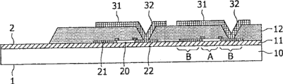
Fig. 7 is illustrated in the encapsulation of the present invention 100 among first embodiment.Device 100 comprises first contact pad 33 and second contact pad 31, and integrated circuit 20.Integrated circuit 20 is present between first and second resin beds 52,12, and first and second resin beds 52,12 place compression strain with circuit, minimizes so that the crack formed. Conductive trajectory 32,34 extends to via pad 21,22 by resin bed 12,52 respectively.In this example, conductive trajectory 32,34 is connected to same via pad 21,22, the encapsulation that generation can apply from two faces 1,2.Yet this is an example, is noted that conductive trajectory 32,34 is offset toward each other in actual applications. Conductive trajectory 32,34 terminates in contact pad 31,33, and contact pad 31,33 exposes (" solder resist qualification pad ") by passivation layer 35,55 parts.Utilizing bump metallization part 36,56 contact-enhancing pads 31,33 in bottom also for its configuration projection 37,57, is solder caps in this example.Passivation layer 55 also extends to insulating barrier 11 on the side direction side 3 of encapsulation 100.Use another resin bed on will encapsulating 100 second 2 such as traditional isolation technics of for example sawing or cutting etc. to separate.
Fig. 8 illustrates second embodiment of encapsulation 100.In the figure, in fact show semi-finished product 200, it is in still attached under the situation on the carrier 40.First feature of present embodiment is not limit contact pad on second 2 of encapsulation.Only use passivation layer 35 covering resin layers 12.Have first resin bed 52 on first 1 of encapsulation 100, define contact pad 34 and conductive trajectory 33 on it, described conductive trajectory 33 extends through first resin bed 52.In this example, projection 57 is traditional projection, for example the projection of those Pb-Sn or SAC scolder (Sn-Ag-Cu).Utilize the hole in first resin bed 52 to limit split tunnel 53.Semi-finished product 200 can be separated into single encapsulation by separating second resin bed 12.This can finish before or after the release products 200 from carrier 40.If after carry out separating step, then before separation resin layer 12, semi-finished product 200 suitably are transferred to separating slices.
Fig. 9 illustrates the 3rd embodiment of encapsulation, and it also is in the stage of the semi-finished product 200 that are attached to carrier 40.This embodiment is structurally identical with first embodiment shown in Figure 6.Difference is that the bottom bump metallization part 36 on the contact pad on second 2 31 does not apply scolder.This is suitable for release products 200 from the carrier.In addition, be stacked to the assembly with another encapsulation if will encapsulate 200, then the scolder of individual quantities is enough.
Figure 10 illustrates the 4th embodiment of encapsulation, and it also is in the stage of the semi-finished product 200 that are attached to carrier 40.In this embodiment, the major part of integrated circuit 20 and resin bed 52,12 is present in the shell of sealing.The sealing shell is formed by passivation layer 35,55, and it extends on resin bed 12,52 and near resin bed 12,52.Passivation layer 55 extends in split tunnel 53, and it obviously is present on all faces.Passivation layer 35 extends to oxide layer 11 by resin bed 12 in circulus 38.It also is particularly suited for protecting the major part of resin bed 12,52, because resin bed easily adsorbed water and pollutant.This may cause the expansion of resin bed.Because passivation layer 35,55 extends to the insulating barrier 11 of the similar characteristic with coupling, so adhere to good with it.Therefore, whole encapsulation is attached to insulating barrier 11, this seems to have improved the stability of the encapsulation under the pressure of high temperature and less degree.The caused stress of difference by the thermal expansion between resin bed 12,52 and the passivation layer 35,55 especially can be discharged by the distortion of resin bed 12,52.
In brief, according to the present invention, flexible encapsulation 100 has semiconductor device 20 between first 1 and second 2, this semiconductor device 20 have attenuate back substrate 10 and interconnection structure.Be used for the contact device 31,33 of outside contact and first resin bed 52 and be present in first 2 of encapsulation 100, this contact device 31,33 is coupled to interconnection structure.On second 2 of semiconductor device 20, be coated with second resin bed 12 at least basically.Contact device 31,33 is present on first resin bed 52 and utilizes the redistribution path 32,34 that extends through first resin bed 52 to be coupled to interconnection structure.Passivation layer 55 covers first resin bed 52 and redistribution path 32,34 at least basically.
Claims (16)
1, a kind of flexible semiconductor encapsulation (100) with first (1) and second (2), between described (1,2), exist and have the back substrate (10) of attenuate and the semiconductor device (20) of interconnection structure, go up contact device (33) and first resin bed (52) that existence is used for outside contact in this first (1), this contact device (33) is coupled to described interconnection structure, and cover by second resin bed (12) at this second (2) the above semiconductor device (20)
Wherein said contact device (33) is present in described first resin bed (52) and goes up and utilize the redistribution path (32,34) that extends in the hole of passing described first resin bed (52) to be coupled to described interconnection structure, and passivation layer (55) covers described first resin bed (52) and described redistribution path (32,34), it is characterized in that described redistribution path (32,34) is not full of the described hole of described first resin bed (52).
2, flexible semiconductor encapsulation as claimed in claim 1, wherein said second resin bed (12) also is coated with passivation layer (35).
3, flexible semiconductor encapsulation as claimed in claim 2, wherein said semiconductor device is provided with the have insulating barrier substrate (10) of (11), and extend to described insulating barrier (11) in hole in the contiguous corresponding described resin bed of described passivation layer (35,55) (12,52) and/or the hole in corresponding described resin bed (12,52), thereby form the shell of the sealing of described semiconductor device (20).
4, encapsulation as claimed in claim 1, wherein said passivation layer (55) comprises inorganic material.
5, flexible semiconductor encapsulation as claimed in claim 1, one of wherein said resin bed (12,52) has the edge of rounding.
6, encapsulation as claimed in claim 1, wherein said semiconductor device (20) is provided with real estate and interconnection face, be present on this real estate and described interconnection structure is present on this interconnection face at semiconductor substrate (10), and wherein said first resin bed (52) is present on the described real estate and described second resin bed (12) is present on the described interconnection face.
7, flexible semiconductor encapsulation as claimed in claim 1, the contact pad of wherein said contact device for coming out by described passivation layer.
8, flexible semiconductor as claimed in claim 2 encapsulation, wherein at least one contact pad is present on described second resin bed and by the hole in the described passivation layer that covers described second resin bed and comes out.
9, a kind of assembly, it comprise as any one described flexible semiconductor encapsulation among the claim 7-8 and another be provided with utilize projection be coupled to as described in the electronic device of contact pad of contact pad.
10, a kind of method that is used to make a plurality of semiconductor packages comprises the steps:
-provide wafer, this wafer to have real estate with relative interconnection face and have a plurality of semiconductor device, described a plurality of semiconductor device have interconnection structure at described interconnect mask;
-on described interconnection structure, apply second resin bed (12);
-utilize adhesive that second (2) corresponding with described interconnection face of described wafer are attached to carrier;
-from first (1) attenuate described wafer corresponding with described real estate;
-on described first of described wafer, apply first resin bed (52), and
-from described carrier, at least some semiconductor packages that form are thus removed,
Wherein contact device is limited on described first resin bed (52), the redistribution path that described contact device utilization extends through the hole in this first resin bed is coupled to described interconnection structure, and passivation layer is applied on described first resin bed and the described redistribution path, it is characterized in that the described hole of described first resin bed of described redistribution path underfill.
11, method as claimed in claim 10 is wherein carried out composition to described first resin bed on described first of described wafer, limiting split tunnel, and applies another passivation layer on first resin bed of described composition.
12, method as claimed in claim 11, wherein said wafer is provided with oxide layer, removes this oxide layer before applying described passivation layer in described split tunnel.
13, method as claimed in claim 11 is wherein carried out composition to described first resin bed on described first of described wafer, so that have the edge of rounding at described split tunnel place.
14, method as claimed in claim 10, wherein said contact device are contact pad, and the form with cap applies scolder on described contact pad.
15, method as claimed in claim 14 wherein has in the groove of required composition by immersion to apply described solder projection.
16, a kind of semi-finished product that comprise a plurality of semiconductor packages as claimed in claim 1, one of wherein said resin bed is continuous between described encapsulation, thereby can make described encapsulation independent by separating described resin bed.
Applications Claiming Priority (2)
| Application Number | Priority Date | Filing Date | Title |
|---|---|---|---|
| EP05101593 | 2005-03-02 | ||
| EP05101593.1 | 2005-03-02 |
Publications (2)
| Publication Number | Publication Date |
|---|---|
| CN101133484A CN101133484A (en) | 2008-02-27 |
| CN100514591C true CN100514591C (en) | 2009-07-15 |
Family
ID=36577514
Family Applications (1)
| Application Number | Title | Priority Date | Filing Date |
|---|---|---|---|
| CNB2006800064736A Expired - Fee Related CN100514591C (en) | 2005-03-02 | 2006-02-27 | A method of manufacturing semiconductor packages and packages made |
Country Status (8)
| Country | Link |
|---|---|
| US (1) | US20080150118A1 (en) |
| EP (1) | EP1856728B1 (en) |
| JP (1) | JP2008532307A (en) |
| CN (1) | CN100514591C (en) |
| AT (1) | ATE412251T1 (en) |
| DE (1) | DE602006003316D1 (en) |
| TW (1) | TW200711081A (en) |
| WO (1) | WO2006092754A2 (en) |
Families Citing this family (15)
| Publication number | Priority date | Publication date | Assignee | Title |
|---|---|---|---|---|
| WO2007004137A2 (en) * | 2005-07-01 | 2007-01-11 | Koninklijke Philips Electronics N.V. | Electronic device |
| WO2007054894A2 (en) * | 2005-11-11 | 2007-05-18 | Koninklijke Philips Electronics N.V. | Chip assembly and method of manufacturing thereof |
| JP4956128B2 (en) * | 2006-10-02 | 2012-06-20 | ルネサスエレクトロニクス株式会社 | Manufacturing method of electronic device |
| US8093689B2 (en) * | 2007-07-02 | 2012-01-10 | Infineon Technologies Ag | Attachment member for semiconductor sensor device |
| US8114708B2 (en) * | 2008-09-30 | 2012-02-14 | General Electric Company | System and method for pre-patterned embedded chip build-up |
| TW201114003A (en) * | 2008-12-11 | 2011-04-16 | Xintec Inc | Chip package structure and method for fabricating the same |
| US8072041B2 (en) * | 2009-04-08 | 2011-12-06 | Finisar Corporation | Passivated optical detectors with full protection layer |
| CN102422338B (en) * | 2009-05-02 | 2015-04-01 | 株式会社半导体能源研究所 | Display device |
| US8212340B2 (en) * | 2009-07-13 | 2012-07-03 | Advanced Semiconductor Engineering, Inc. | Chip package and manufacturing method thereof |
| US8952519B2 (en) * | 2010-01-13 | 2015-02-10 | Chia-Sheng Lin | Chip package and fabrication method thereof |
| JP5521862B2 (en) * | 2010-07-29 | 2014-06-18 | 三菱電機株式会社 | Manufacturing method of semiconductor device |
| US10446442B2 (en) * | 2016-12-21 | 2019-10-15 | Globalfoundries Inc. | Integrated circuit chip with molding compound handler substrate and method |
| KR20180136148A (en) * | 2017-06-14 | 2018-12-24 | 에스케이하이닉스 주식회사 | Semiconductor device having bump |
| KR102435517B1 (en) * | 2018-04-12 | 2022-08-22 | 에스케이하이닉스 주식회사 | Chip stack package |
| KR102545168B1 (en) | 2019-03-26 | 2023-06-19 | 삼성전자주식회사 | Interposer and semiconductor package including the same |
Family Cites Families (14)
| Publication number | Priority date | Publication date | Assignee | Title |
|---|---|---|---|---|
| FR2599893B1 (en) * | 1986-05-23 | 1996-08-02 | Ricoh Kk | METHOD FOR MOUNTING AN ELECTRONIC MODULE ON A SUBSTRATE AND INTEGRATED CIRCUIT CARD |
| US5386623A (en) * | 1990-11-15 | 1995-02-07 | Hitachi, Ltd. | Process for manufacturing a multi-chip module |
| US5336928A (en) * | 1992-09-18 | 1994-08-09 | General Electric Company | Hermetically sealed packaged electronic system |
| EP1041624A1 (en) * | 1999-04-02 | 2000-10-04 | Interuniversitair Microelektronica Centrum Vzw | Method of transferring ultra-thin substrates and application of the method to the manufacture of a multilayer thin film device |
| US6242282B1 (en) * | 1999-10-04 | 2001-06-05 | General Electric Company | Circuit chip package and fabrication method |
| US6734534B1 (en) * | 2000-08-16 | 2004-05-11 | Intel Corporation | Microelectronic substrate with integrated devices |
| US6720270B1 (en) * | 2000-09-13 | 2004-04-13 | Siliconware Precision Industries Co., Ltd. | Method for reducing size of semiconductor unit in packaging process |
| US6586276B2 (en) * | 2001-07-11 | 2003-07-01 | Intel Corporation | Method for fabricating a microelectronic device using wafer-level adhesion layer deposition |
| TW517361B (en) * | 2001-12-31 | 2003-01-11 | Megic Corp | Chip package structure and its manufacture process |
| JP4100936B2 (en) * | 2002-03-01 | 2008-06-11 | Necエレクトロニクス株式会社 | Manufacturing method of semiconductor device |
| US6798057B2 (en) * | 2002-11-05 | 2004-09-28 | Micron Technology, Inc. | Thin stacked ball-grid array package |
| JP4056854B2 (en) * | 2002-11-05 | 2008-03-05 | 新光電気工業株式会社 | Manufacturing method of semiconductor device |
| US7180149B2 (en) * | 2003-08-28 | 2007-02-20 | Fujikura Ltd. | Semiconductor package with through-hole |
| WO2005117096A1 (en) * | 2004-05-31 | 2005-12-08 | Sharp Takaya Electronics Industry Co., Ltd. | Circuit module manufacturing method and circuit module manufactured by the method |
-
2006
- 2006-02-27 CN CNB2006800064736A patent/CN100514591C/en not_active Expired - Fee Related
- 2006-02-27 DE DE602006003316T patent/DE602006003316D1/en not_active Expired - Fee Related
- 2006-02-27 WO PCT/IB2006/050599 patent/WO2006092754A2/en not_active Application Discontinuation
- 2006-02-27 JP JP2007557647A patent/JP2008532307A/en active Pending
- 2006-02-27 AT AT06710970T patent/ATE412251T1/en not_active IP Right Cessation
- 2006-02-27 EP EP06710970A patent/EP1856728B1/en not_active Not-in-force
- 2006-02-27 US US11/816,750 patent/US20080150118A1/en not_active Abandoned
- 2006-03-01 TW TW095106862A patent/TW200711081A/en unknown
Also Published As
| Publication number | Publication date |
|---|---|
| WO2006092754A2 (en) | 2006-09-08 |
| JP2008532307A (en) | 2008-08-14 |
| WO2006092754A3 (en) | 2007-01-18 |
| EP1856728B1 (en) | 2008-10-22 |
| EP1856728A2 (en) | 2007-11-21 |
| TW200711081A (en) | 2007-03-16 |
| ATE412251T1 (en) | 2008-11-15 |
| DE602006003316D1 (en) | 2008-12-04 |
| US20080150118A1 (en) | 2008-06-26 |
| CN101133484A (en) | 2008-02-27 |
Similar Documents
| Publication | Publication Date | Title |
|---|---|---|
| CN100514591C (en) | A method of manufacturing semiconductor packages and packages made | |
| US9893213B2 (en) | Method of forming a wire bond sensor package | |
| JP2008532307A5 (en) | ||
| US8502380B2 (en) | Chip package and fabrication method thereof | |
| US6768207B2 (en) | Multichip wafer-level package and method for manufacturing the same | |
| US6838762B2 (en) | Water-level package with bump ring | |
| US20090127702A1 (en) | Package, subassembly and methods of manufacturing thereof | |
| US8860195B2 (en) | Apparatus and method for increasing the quantity of discrete electronic components in an integrated circuit package | |
| JP2009500820A (en) | Method and assembly for manufacturing an assembly | |
| KR20060088518A (en) | Semiconductor device and manufacturing method thereof | |
| US20090309218A1 (en) | Semiconductor device and method of manufacturing the same | |
| US20080290511A1 (en) | Chip Assembly and Method of Manufacturing Thereof | |
| CN113314477A (en) | Semiconductor device and method for manufacturing semiconductor device | |
| JP4828515B2 (en) | Manufacturing method of semiconductor device | |
| US10115673B1 (en) | Embedded substrate package structure | |
| CN109003946B (en) | Package structure and method for manufacturing the same | |
| KR20090052282A (en) | Semiconductor device and manufacturing method thereof | |
| US20230002217A1 (en) | Semiconductor devices and related methods | |
| US20230097173A1 (en) | Type of bumpless and wireless semiconductor device | |
| US20210104465A1 (en) | Electronic package, packaging substrate, and methods for fabricating the same | |
| KR100523298B1 (en) | Semiconductor chip having Au bump and manufacturing method thereof | |
| US20090324906A1 (en) | Semiconductor with top-side wrap-around flange contact | |
| KR101123798B1 (en) | Method of fabricating for wafer level chip scale package | |
| JP2008218949A (en) | Semiconductor device and manufacturing method therefor | |
| JP2006100580A (en) | Method for manufacturing semiconductor device |
Legal Events
| Date | Code | Title | Description |
|---|---|---|---|
| C06 | Publication | ||
| PB01 | Publication | ||
| C10 | Entry into substantive examination | ||
| SE01 | Entry into force of request for substantive examination | ||
| C14 | Grant of patent or utility model | ||
| GR01 | Patent grant | ||
| C17 | Cessation of patent right | ||
| CF01 | Termination of patent right due to non-payment of annual fee |
Granted publication date: 20090715 Termination date: 20100227 |