CN100481732C - Method and device for performing full bridge integral noise shaping for quantization of pulse width modulation signals - Google Patents
Method and device for performing full bridge integral noise shaping for quantization of pulse width modulation signals Download PDFInfo
- Publication number
- CN100481732C CN100481732C CNB038229714A CN03822971A CN100481732C CN 100481732 C CN100481732 C CN 100481732C CN B038229714 A CNB038229714 A CN B038229714A CN 03822971 A CN03822971 A CN 03822971A CN 100481732 C CN100481732 C CN 100481732C
- Authority
- CN
- China
- Prior art keywords
- full
- signal
- pulse
- equation
- bridge
- Prior art date
- Legal status (The legal status is an assumption and is not a legal conclusion. Google has not performed a legal analysis and makes no representation as to the accuracy of the status listed.)
- Expired - Fee Related
Links
- 238000007493 shaping process Methods 0.000 title claims abstract description 37
- 238000013139 quantization Methods 0.000 title claims abstract description 34
- 238000000034 method Methods 0.000 title claims abstract description 33
- 238000006243 chemical reaction Methods 0.000 claims abstract description 13
- 230000010354 integration Effects 0.000 claims description 30
- 230000000295 complement effect Effects 0.000 claims description 17
- 230000001915 proofreading effect Effects 0.000 claims description 3
- 238000004422 calculation algorithm Methods 0.000 abstract description 19
- 238000012937 correction Methods 0.000 abstract description 14
- 238000001228 spectrum Methods 0.000 description 15
- 230000008569 process Effects 0.000 description 12
- 238000010586 diagram Methods 0.000 description 10
- 238000011002 quantification Methods 0.000 description 10
- 238000004088 simulation Methods 0.000 description 9
- 238000005070 sampling Methods 0.000 description 7
- 230000002146 bilateral effect Effects 0.000 description 5
- 230000004048 modification Effects 0.000 description 4
- 238000012986 modification Methods 0.000 description 4
- 238000012545 processing Methods 0.000 description 4
- 238000005094 computer simulation Methods 0.000 description 3
- 230000003595 spectral effect Effects 0.000 description 3
- 230000015556 catabolic process Effects 0.000 description 2
- 230000008878 coupling Effects 0.000 description 2
- 238000010168 coupling process Methods 0.000 description 2
- 238000005859 coupling reaction Methods 0.000 description 2
- 239000013078 crystal Substances 0.000 description 2
- 238000006731 degradation reaction Methods 0.000 description 2
- 238000005516 engineering process Methods 0.000 description 2
- 238000001914 filtration Methods 0.000 description 2
- 230000013011 mating Effects 0.000 description 2
- 230000000630 rising effect Effects 0.000 description 2
- MKYBYDHXWVHEJW-UHFFFAOYSA-N N-[1-oxo-1-(2,4,6,7-tetrahydrotriazolo[4,5-c]pyridin-5-yl)propan-2-yl]-2-[[3-(trifluoromethoxy)phenyl]methylamino]pyrimidine-5-carboxamide Chemical compound O=C(C(C)NC(=O)C=1C=NC(=NC=1)NCC1=CC(=CC=C1)OC(F)(F)F)N1CC2=C(CC1)NN=N2 MKYBYDHXWVHEJW-UHFFFAOYSA-N 0.000 description 1
- 238000009825 accumulation Methods 0.000 description 1
- 238000004590 computer program Methods 0.000 description 1
- 230000001419 dependent effect Effects 0.000 description 1
- 230000005669 field effect Effects 0.000 description 1
- 230000008676 import Effects 0.000 description 1
- 230000006872 improvement Effects 0.000 description 1
- 238000012797 qualification Methods 0.000 description 1
- 230000009467 reduction Effects 0.000 description 1
- 230000007704 transition Effects 0.000 description 1
Images


Classifications
-
- H—ELECTRICITY
- H03—ELECTRONIC CIRCUITRY
- H03M—CODING; DECODING; CODE CONVERSION IN GENERAL
- H03M1/00—Analogue/digital conversion; Digital/analogue conversion
- H03M1/06—Continuously compensating for, or preventing, undesired influence of physical parameters
- H03M1/0617—Continuously compensating for, or preventing, undesired influence of physical parameters characterised by the use of methods or means not specific to a particular type of detrimental influence
- H03M1/0675—Continuously compensating for, or preventing, undesired influence of physical parameters characterised by the use of methods or means not specific to a particular type of detrimental influence using redundancy
- H03M1/0678—Continuously compensating for, or preventing, undesired influence of physical parameters characterised by the use of methods or means not specific to a particular type of detrimental influence using redundancy using additional components or elements, e.g. dummy components
- H03M1/068—Continuously compensating for, or preventing, undesired influence of physical parameters characterised by the use of methods or means not specific to a particular type of detrimental influence using redundancy using additional components or elements, e.g. dummy components the original and additional components or elements being complementary to each other, e.g. CMOS
- H03M1/0682—Continuously compensating for, or preventing, undesired influence of physical parameters characterised by the use of methods or means not specific to a particular type of detrimental influence using redundancy using additional components or elements, e.g. dummy components the original and additional components or elements being complementary to each other, e.g. CMOS using a differential network structure, i.e. symmetrical with respect to ground
-
- H—ELECTRICITY
- H03—ELECTRONIC CIRCUITRY
- H03M—CODING; DECODING; CODE CONVERSION IN GENERAL
- H03M7/00—Conversion of a code where information is represented by a given sequence or number of digits to a code where the same, similar or subset of information is represented by a different sequence or number of digits
-
- H—ELECTRICITY
- H03—ELECTRONIC CIRCUITRY
- H03F—AMPLIFIERS
- H03F3/00—Amplifiers with only discharge tubes or only semiconductor devices as amplifying elements
- H03F3/20—Power amplifiers, e.g. Class B amplifiers, Class C amplifiers
- H03F3/21—Power amplifiers, e.g. Class B amplifiers, Class C amplifiers with semiconductor devices only
- H03F3/217—Class D power amplifiers; Switching amplifiers
- H03F3/2173—Class D power amplifiers; Switching amplifiers of the bridge type
-
- H—ELECTRICITY
- H03—ELECTRONIC CIRCUITRY
- H03K—PULSE TECHNIQUE
- H03K7/00—Modulating pulses with a continuously-variable modulating signal
- H03K7/08—Duration or width modulation ; Duty cycle modulation
-
- H—ELECTRICITY
- H03—ELECTRONIC CIRCUITRY
- H03M—CODING; DECODING; CODE CONVERSION IN GENERAL
- H03M3/00—Conversion of analogue values to or from differential modulation
- H03M3/04—Differential modulation with several bits, e.g. differential pulse code modulation [DPCM]
-
- H—ELECTRICITY
- H03—ELECTRONIC CIRCUITRY
- H03F—AMPLIFIERS
- H03F2200/00—Indexing scheme relating to amplifiers
- H03F2200/351—Pulse width modulation being used in an amplifying circuit
-
- H—ELECTRICITY
- H03—ELECTRONIC CIRCUITRY
- H03M—CODING; DECODING; CODE CONVERSION IN GENERAL
- H03M1/00—Analogue/digital conversion; Digital/analogue conversion
- H03M1/12—Analogue/digital converters
- H03M1/50—Analogue/digital converters with intermediate conversion to time interval
- H03M1/504—Analogue/digital converters with intermediate conversion to time interval using pulse width modulation
Landscapes
- Engineering & Computer Science (AREA)
- Theoretical Computer Science (AREA)
- Power Engineering (AREA)
- Amplifiers (AREA)
- Compression, Expansion, Code Conversion, And Decoders (AREA)
- Analogue/Digital Conversion (AREA)
Abstract
Systems and methods are described for full bridge integral noise shaping for quantization of pulse width modulated signals. A method for full bridge integral noise shaping comprises: receiving a first and a second reference PWM signal (401, 402); summing the first and second reference PWM signals with a quantization error correction (504); quantizing the sum into a first and a second output PWM signal (404, 405); differentially integrating the first and second reference PWM signals and the first and second output PWM signals according to a full bridge integral noise shaping algorithm to obtain the quantization error correction. An apparatus for performing a full bridge integralnoise shaping quantization of a pulse modulated signal, includes: a single-ended to differential conversion circuit (203); and a full bridge INS quantizer circuit (403), coupled to the single-ended to differential conversion circuit.
Description
Technical field
The present invention relates generally to the digital amplifier field.More particularly, the present invention relates to the processing of pulse-modulated signal.
Background technology
Traditionally, audio frequency amplifier is worked in analog domain.These amplifiers often have lower power conversion efficiency, therefore have bigger size and weight.Along with the particularly appearance of digital audio source of digital technology, beginning is carried out audio frequency and is amplified in numeric field.
Use the digital audio amplifier of pulse width modulation (PWM) to have the power conversion efficiency higher, and have fixing switching frequency than analogue amplifier.Be different from the simulation PWM that uses analog ramp signal etc. to quantize, quantize and generate digital PWM by the circulation of high-frequency clock is counted.
The U.S. Patent No. 6,414,613 of Midya has been described a kind of integrated noise shaping (integral noise shaping, INS) algorithm of the PWM of quantification waveform.Because the noise that the quantification duty cycle signals produces drops on outside the interested frequency band, use PWM noise shaping ring to improve signal to noise ratio (snr) in the band that quantizes pwm signal by forcing.
In using, often uses the full-bridge with four switches switching amplifier based on pulse width modulation.In such application, can adopt one-sided (single-sided) PWM to handle, anti-phase then resulting signal, right to create the required signal of driving full bridge power level.U.S. Patent No. 6,414,613 is such examples.
In order to use prior art to obtain high s/n ratio, for crystal reference clock frequency, output filtering, in power stage coupling and in signal path, mating, have strict requirement.
Summary of the invention
Existence is to the needs of following embodiment.Certainly, the invention is not restricted to these embodiment.
According to an aspect of the present invention, a kind of method that is used for the shaping of full-bridge integrated noise comprises: receive first and second with reference to pwm signal; Sue for peace with reference to pwm signal and quantization error correction first and second; Should and be quantized into first and second output pwm signals; According to full-bridge integrated noise shaping algorithm, carry out the difference integration to first and second with reference to the pwm signal and first and second output pwm signals, proofread and correct to obtain quantization error.According to a further aspect in the invention, a kind of equipment that is used for paired pulses modulation signal execution full-bridge integrated noise shaping quantization, comprising: single-ended (single-ended) is to the differential conversion circuit; And full-bridge INS sample circuit, be couple to the single-ended-to-difference change-over circuit.
According to a further aspect in the invention, provide a kind of method that is used for the shaping of full-bridge integrated noise, having comprised: received the first and second reference pulse modulation signals; Proofreading and correct with quantization error one of at least in the first and second reference pulse modulation signals sued for peace, with obtain and; Quantize should and, to produce first and second pulse-modulated signals that quantize; And the pulse-modulated signals that the first and second reference pulse modulation signals and first and second are quantized carry out the difference integration, proofread and correct to obtain quantization error.
According to another aspect of the invention, a kind of equipment that the paired pulses modulation signal is carried out full-bridge integrated noise shaping quantization that is used for is provided, comprise: the single-ended-to-difference change-over circuit is used for single sided pulse modulation signal differential conversion is become first pulse-modulated signal and second pulse-modulated signal; And full-bridge integrated noise shaping quantization circuit, be couple to the single-ended-to-difference change-over circuit, comprise: summation and sample circuit, be couple to the single-ended-to-difference change-over circuit, be used for first and second pulse-modulated signals one of at least with quantization error proofread and correct sue for peace with obtain and, and be used for quantizing should and, to produce first pulse-modulated signal that quantizes and second pulse-modulated signal that quantizes; And the difference product parallel circuit, be couple to summation and sample circuit, be used for first and second pulse-modulated signals and first and second pulse-modulated signals that quantize are carried out the difference integration, proofread and correct to obtain quantization error.
When in conjunction with describing below when considering with accompanying drawing, these and other embodiment of the present invention will become apparent and better understand.Yet, should be appreciated that to describe below although understand various embodiment of the present invention and numerous specific detail thereof, but it only provides as example, and does not provide constraints.Under the situation that does not break away from spirit of the present invention, can carry out various replacements, modification within the scope of the invention, replenish and/or rearrange, and the present invention includes all such replacements, modification, replenish and/or rearrange.
Description of drawings
Follow this specification and form its a part of accompanying drawing and comprise in order to describe particular aspects of the present invention.By with reference to illustrated in the accompanying drawings exemplary be nonrestrictive embodiment thus, each assembly of the present invention and the system that comprises thereof and operation know that notion will become easier and understand that wherein identical label (if they appear in a plurality of accompanying drawings) is specified identical unit.By in conjunction with description given here one or more with reference in these accompanying drawings, the present invention can be better understood.Should be noted that what parts shown in the drawings were not necessarily drawn in proportion.
Fig. 1 is the circuit diagram of the full bridge power level of amplifier.
Fig. 2 is the block diagram of PWM processing scheme.
Fig. 3 is the sequential chart of PWM INS quantizing process.
Fig. 4 is the block diagram of the full-bridge INS quantization scheme of the expression embodiment of the invention.
Fig. 5 is the more detailed block diagram of the full-bridge INS quantization scheme of the expression embodiment of the invention.
Fig. 6 is the sequential chart of the vectorial full-bridge INS process of the expression embodiment of the invention.
Fig. 7 is the simulated power spectrum density figure of the vectorial full-bridge INS output signal of the expression embodiment of the invention.
Fig. 8 is the simulated power spectrum density figure with 0.3% mismatch of the vectorial full-bridge INS output signal of the expression embodiment of the invention.
Fig. 9 is the sequential chart of the complementary full-bridge INS process of the expression embodiment of the invention.
Figure 10 is the simulated power spectrum density figure of the complementary full-bridge INS output signal of the expression embodiment of the invention.
Figure 11 is the simulated power spectrum density figure with 0.3% mismatch of the complementary full-bridge INS output signal of the expression embodiment of the invention.
Figure 12 is the simulated power spectrum density figure with 1% mismatch of the complementary full-bridge INS output signal of the expression embodiment of the invention.
Figure 13 be the expression embodiment of the invention with the skew of twice switching frequency operation sequential chart with reference to full-bridge INS process.
Figure 14 be the expression embodiment of the invention with the skew of twice switching frequency operation simulation output power spectrum density map with reference to full-bridge INS output signal.
Figure 15 be the expression embodiment of the invention with the skew of four times of switching frequencies operation sequential chart with reference to full-bridge INS process.
Figure 14 be the expression embodiment of the invention with the skew of four times of switching frequencies operation simulation output power spectrum density map with reference to full-bridge INS output signal.
Figure 17 is the simulation output spectrum figure of single-ended INS output signal.
Figure 18 is the simulation output spectrum figure of the full-bridge INS output signal of the expression embodiment of the invention.
Embodiment
With reference to non-limiting example shown in the drawings and that describe in detail hereinafter, the present invention and various characteristics thereof and preferred details are described more fully.Should be appreciated that this detailed description and specific examples although understand specific embodiment of the present invention, but it provides as example just, and do not provide constraints.By present disclosure, the spirit of basic inventive concept and/or the various replacements in the scope, modification, replenish and/or rearrange and to become clear for the ordinary skill in the art.
With reference to Fig. 1, it shows the circuit diagram of full bridge power level 100 amplifiers of prior art.One group of four the switch 102-105 that comprises p raceway groove and n slot field-effect transistor (FET) be couple to supply voltage 101, load 106 and reference voltage () 107.Input 108 is couple to first side of full bridge power level 100, and another input 108 is couple to second side of full bridge power level 100.The operation of full bridge power level 100 and characteristic and variant thereof are known in the present technique field.
In using, often uses the full-bridge with four switches based on pulse modulated switching amplifier.Can use dissimilar pulse modulation drive signals, for example pulse width modulation (PWM) signal and pulse density modulated signal (PDM).Relate to the PWM drive signal though describe below, those of ordinary skill in the art will be appreciated that the present invention also is applicable to the pulse-modulated signal of other types.
Typically, PWM handles and comprises quantification and noise shaping.In the prior art, this processing should be used for finishing based on one-sided or half-bridge.In typical full-bridge is used, adopt one-sided PWM to handle, anti-phase then resulting signal is driven into two required differential driving signals of full bridge power level thereby create with a pair of input.
With reference to Fig. 2, it shows the block diagram of the PWM processing scheme of prior art.Non-quantized pwm signal 200 is handled by integrated noise shaping (INS) quantizer 201, quantizes pwm signal 202 thereby produce.Quantize pwm signal 202 and further processed by single-ended-to-difference conversion block 203, thereby export a pair of differential quantization full bridge PWM signal 204, it can drive the full bridge power level 100 that is couple to load 106 together.
Still with reference to Fig. 2, INS quantizer 201 comprises PWM noise shaping ring, and it is used for improving signal to noise ratio in the band that quantizes pwm signal.The input of this ring is the high-resolution digital signal of expression duty ratio series.The output of this ring is the low resolution digital signal of representation class like duty ratio series.The noise shaping ring can force the noise (error) that produces owing to the quantification duty cycle signals to remain on outside the interested frequency spectrum.Noise shaping can provide data pilot adjustment (data directed adjustment) based on the quantization error vector output sample of previous accumulation.
With reference to Fig. 3, it shows the sequential chart 300 of the PWM INS quantizing process of prior art.Non-quantized pwm signal X (t) the 200th, thus the integrated noise that quantizes pwm signal Y (t) 202 produced by INS quantizer 201 shapings shown in Figure 2.Also with reference to the bilateral slope sampled signal of in natural sample circuit (not shown), using 310.The longitudinal axis is represented signal 200 and 202, and the transverse axis express time.The interested time comprises: (n-1) Ts, (n-1/2) Ts, nTs, (n+1/2) Ts and (n+1) Ts, and wherein Ts is a switch periods, and n is an integer.
Still with reference to Fig. 3, the INS algorithm can calculate the integral feedback that quantizes Y (t) 202 and do not quantize the noise between X (t) the 200PWM signal.Integral is used for quantizing noise is carried out shaping.Might arrive any rank with analysis mode (analytically) integration PWM waveform, and use identical integration ring to quantize the rising and falling edges of PWM.For example, can use fourth-order system to come integration input X (t) 200 and the error of exporting between the Y (t) 202.These integrations are:
Equation 1-4 calculate since the error that the quantification to pwm signal produces first to the quadravalence integration, it can be divided into a left side half circulation (l) and right partly circulate (r).Still with reference to Fig. 3, with discrete time interval defining integration (I
1, I
2, I
3And I
4), and can calculate it with analysis mode.The semi-cyclic value in a left side is:
Il
1(n)=I
1(nT
s)=ir
1(n-1)+((1-yr (n-1))-(1-xr (n-1))) equation 5
And right semi-cyclic value is:
Equation 5-8 calculate the error that produces owing to left semi-cyclic quantification to pwm signal first to the quadravalence integration.Equation 9-12 calculate the error that produces owing to right semi-cyclic quantification to pwm signal first to the quadravalence integration.These closed form integral equations allow to carry out calculating with switching frequency.
Left and right semi-cyclic correction duty ratio (being respectively zl (n) and zr (n)) is as giving a definition:
Zl (n)=xl (n)+k
1Il
1(n)+k
2Il
2(n)+k
3Il
3(n)+k
4Il
4(n) equation 13
Zr (n)=xr (n)+k
1Ir
1(n)+k
2Ir
2(n)+k
3Ir
3(n)+k
4Ir
4(n) equation 14
Wherein the K value is corresponding to the weighted factor of a plurality of integrators of noise shaping filter.
Quantize to be fit to the clock circulation of integer number proofreading and correct duty factor (duty cycle).This causes quantization error e, and its error as circulation in the future is fed back to the INS ring:
Yl (n)=Quantize (zl (n))=Q (zl (n))=zl (n)+el (n) equation 15
Yr (n)=Quantize (zr (n))=Q (zr (n))=zr (n)+er (n) equation 16
The present invention includes a kind of method and/or equipment that quantizes PWM and carry out full-bridge integrated noise shaping (INS) that is used to.In one embodiment, the present invention includes a series of INS algorithms, it quantizes pwm signal, to produce two different PWM waveforms.Pass through present disclosure, those of ordinary skill in the art can recognize, full bridge PWM is handled and can be improved signal to noise ratio (snr), and reduces crystal reference clock frequency, output LC filtering, the coupling and the requirement of mating in reference path in power stage.It also can allow lower switching frequency.
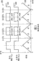
With reference to Fig. 4, it shows the block diagram of full-bridge INS quantization scheme according to an embodiment of the invention.Quantized signal 200 is not handled by single-ended-to-difference conversion block 203, thereby produces first and second with reference to (difference does not quantize) pwm signal 401 and 402.Single-ended-to-difference conversion block 203 also can suppress the carrier signal (if having) in the quantized signal 200 not.This is further processed by full-bridge INS quantiser block 403 reference signal 401 and 402, quantizes full bridge PWM signal 404 and 405 thereby produce first and second, and it can drive the full bridge power level 100 that is couple to load 106.
Still with reference to Fig. 4, this can operate by different INS in the reference signal 401 and 402 each and quantize, thereby produces a pair of different quantification full bridge PWM signal 404 and 405.According to an aspect of the present invention, this provides additional switch edge to pwm signal, and it provides additional sample, and therefore the chance that improves performance is provided.In one embodiment, the invention provides a pair of different quantification full bridge PWM signal 404 and 405, it has complementary duty ratio.In another embodiment, the invention provides a kind of method and apparatus that is used in each switch periods, carrying out INS operation at least twice.
With reference to Fig. 5, it shows the more more detailed block diagram of full-bridge INS quantization scheme.Pulse code modulation (pcm) signal 500 is input in the nature sampler 501, the single-ended pwm signal 200 of wherein natural sampler 501 outputs.Single-ended pwm signal 200 is handled by single-ended-to-difference conversion block 203, thus produce first with reference to pwm signal 401 and second with reference to pwm signal 402.But single-ended-to-difference conversion block 203 is suppressed carrier also in case of necessity.This further processes reference pwm signal 401 and 402 summation and quantize block 502 by full-bridge INS quantizer 403, thereby produces first output pwm signal 404 and second output pwm signal 405.This can be used to drive first and second sides of full bridge power level 100 to output pwm signal 404 and 405.The difference product piecemeal of full-bridge INS quantizer 403 receive with reference to pwm signal to 401 and 402 and output pwm signal to 404 and 405, calculate and quantize error correction 504, and it is fed to summation and quantize block 502.
Still with reference to Fig. 5, difference product piecemeal 503 can utilize first and second to carry out independently difference integration operation with reference to pwm signal 401 and 402 and first and second output pwm signals 404 and 405.Difference product piecemeal 503 also can calculate and quantize error correction value 504, and it is added to first and second with reference to pwm signal 401 and 402 by summation and quantize block 502, to reduce quantizing noise.
Generally speaking, according to the present invention, by algorithm, the utilization quantification error correction 504 that is referred to herein as full-bridge integrated noise shaping algorithm, the operation of passing through summation and quantize block 502 and difference product piecemeal 503, produce two output pwm signals 404 and 405 as two functions with reference to pwm signal 401 and 402.The specific examples of full-bridge integrated noise shaping algorithm is provided below with reference to example 1-4.
Example
, further describe specific embodiment of the present invention now by the following non-limitative example that is used for quite at length setting forth each characteristic.Following example can be implemented mode of the present invention and comprises in order to help to understand.Should be appreciated that following example represents to be found to be the good embodiment that works in the embodiment of this invention, so they can be considered to constitute and implement optimal way of the present invention.Yet, should be appreciated that under the situation that does not break away from the spirit and scope of the present invention, can in these exemplary embodiments, carry out various modifications, still obtain identical or similar result simultaneously.Thereby these examples should not be interpreted as limiting the scope of the invention.
Example 1
Vector full-bridge INS
In the present embodiment, vectorial full-bridge INS algorithm produces and allows diverse each other first and second output pwm signals.Each output full bridge PWM signal can drive a side of full bridge power level 100 shown in Figure 1, promptly independently duty ratio be applied to full bridge power level 100 each partly.
With reference to Fig. 6, it shows the sequential chart 600 of vectorial full-bridge INS process.The longitudinal axis is represented signal 401A, 402A, 404A and 405A, and the transverse axis express time.The interested time comprises (2n-1) Ts/2, (2n) Ts/2 and (2n+1) Ts/2, and wherein n is an integer, and Ts is a switch periods.A pair ofly be applied to full-bridge INS quantizer 403 shown in Figure 4 with reference to pwm signal 401A and 402A, it exports a pair of output pwm signal 404A and 405A.Notice that negative reference signal 402A is delay and the inverted version of positive reference signal 401A.With reference to the bilateral slope sampled signal of in natural sample circuit 501 shown in Figure 5, using 610.Vector full-bridge INS algorithm is as follows:
For the right side half circulation (r), at time t=(2n-1) Ts/2:
Xr
1(n-1)=xr (n-1) equation 17
Xr
2(n-1)=1-xl (n-1) equation 18
z
1=xr
1+ k
1I
1+ k
2I
2+ k
3I
3+ k
4I
4Equation 19
y
1=Quantize (z
1)=Q (z
1) equation 20
z
2=xr
2-(k
1I
1+ k
2I
2+ k
3I
3+ k
4I
4)+(y
1-z
1) equation 21
y
2=Quantize (z
2)=Q (z
2) equation 22
Equation 17 and 18 is set up with reference to pwm signal the relation between the right side half circulation of 401A and 402A.Equation 19 and 21 is as with reference to the function definition output pwm signal of pwm signal 401A and the 402A correction duty ratio to 404A and 405A, and wherein the k value is corresponding to weighted factor.Operation shown in the equation 19-22 is by difference product piecemeal 503 all shown in Figure 5 and summation and quantize block 502 execution.
Upgrade integration at time t=(2n) Ts/2:
I
1=I
1+ (1-y
1)-(1-xr
1)-(1-y
2)+(1-xr
2) equation 26
Integration shown in the equation 23-26 is carried out by differential integrator shown in Figure 5 503, and provides quantization error to proofread and correct 504.For a left side half circulation (l), at time t=(2n) Ts/2:
Xl
1) n)=xl (n) equation 27
Xl
2(n)=1-xr (n-1) equation 28
z
1=xl
1+ k
1I
1+ k
2I
2+ k
3I
3+ k
4I
4Equation 29
y
1=Quantize (z
1)=Q (z
1) equation 30
z
2=xl
2-(k
1I
1+ k
2I
2+ k
3I
3+ k
4I
4)+(y
1-z
1) equation 31
y
2=Quantize (z
2)=Q (z
2) equation 32
Equation 27 and 28 is set up with reference to pwm signal the relation between a left side half circulation (l) of 401A and 402A.Equation 29 and 31 is as with reference to the function definition output pwm signal of pwm signal 401A and the 402A correction duty ratio to 404A and 405A.Upgrade integration at time t=(2n+1) Ts/2:
I
1=I
1-xl
2+ y
2+ xl
1-y
1Equation 36
Integration shown in the equation 33-36 is carried out by differential integrator shown in Figure 5 503, and provides quantization error to proofread and correct 504.
With reference to Fig. 7, it shows the computer simulation power spectral density plot 700 of vectorial full-bridge INS output signal.Input is the full-scale tone of 15kHz (full scale tone).Figure 70 0 is the result who does not have the vectorial full-bridge INS of mismatch to use between the both sides of as shown in Figure 1 power stage 100.The longitudinal axis represents to be applied to the amplitude (dB) of the differential signal of load 106, and transverse axis is represented the frequency (* 10 of signal
4).
With reference to Fig. 8, it shows the computer simulation power spectral density plot 800 with 0.3% mismatch of vectorial full-bridge INS output signal.Figure 80 0 is the result who exists this moment another vectorial full-bridge INS of 0.3% mismatch to use between the both sides of as shown in Figure 1 power stage 100.The longitudinal axis represents to be applied to the amplitude (dB) of the differential signal of load 106, and transverse axis is represented the frequency (* 10 of signal
4Hz).Notice that compare with Fig. 7, noise level significantly raises.0.3% mismatch is illustrated in the mismatch that may find in the integrated power level.Next example is that complementary full-bridge INS describes the optional embodiment that the power stage mismatch is had more tolerance.
Example 2
Complementary full-bridge INS
In the present embodiment, complementary full-bridge INS algorithm produces first and second output pwm signals with complementary duty cycle.Each output full bridge PWM signal can drive a side of full bridge power level 100 shown in Figure 1, the duty ratio of complementation can be applied to full bridge power level 100 each half.
With reference to Fig. 9, it shows the sequential chart 900 of complementary full-bridge INS process.The longitudinal axis is represented signal 401B, 402B, 404B and 405B, and the transverse axis express time.The interested time comprises (2n-1) Ts/2, (2n) Ts/2 and (2n+1) Ts/2, and wherein n is an integer, and Ts is a switch periods.A pair ofly be applied to full-bridge INS quantizer 403 shown in Figure 4 with reference to pwm signal 401B, 402B, it exports a pair of output pwm signal 404B and 405B.With reference to the bilateral slope sampled signal of in natural sample circuit 501 shown in Figure 5, using 910.Complementary full-bridge INS algorithm is as follows:
For the right side half circulation (r), at time t=(2n-1) Ts/2:
Xr
1(n-1)=xr (n-1) equation 37
Xr
2(n-1)=1-xl (n-1) equation 38
y
1=Quantize (z
1)=Q (z
1) equation 40
y
2=1-y
1Equation 41
Equation 37 and 38 is set up with reference to pwm signal the relation between the right side half circulation of 401B and 402B.Equation 39 conducts are with reference to the correction duty ratio of the function definition output pwm signal 404B of pwm signal 401B and 402B, and wherein the k value is corresponding to weighted factor.Operation shown in the equation 39-41 is by difference product piecemeal 503 all shown in Figure 5 and summation and quantize block 502 execution.Upgrade integration at time t=(2n) Ts/2:
I
1=I
1+ (1-y
1)-(1-xr
1)-(1-y
2)+(1-xr
2) equation 45
Integration shown in the equation 42-45 is carried out by differential integrator shown in Figure 5 503, and provides quantization error to proofread and correct 504.For a left side half circulation (l), at time t=(2n) Ts/2:
Xl
1(n)=xl (n) equation 46
Xl
2(n)=1-xr (n-1) equation 47
y
1=Q (z
1) equation 49
y
2=1-y
1Equation 50
Equation 46 and 47 is set up with reference to pwm signal the relation between a left side half circulation of 401B and 402B.Equation 48 conducts are with reference to the correction duty ratio of the function definition output pwm signal 404B of pwm signal 401B and 402B.Upgrade integration at time t=(2n+1) Ts/2:
I
1=I
1-xl
2+ y
2+ xl
1-y
1Equation 54
Integration shown in the equation 51-54 is carried out by differential integrator shown in Figure 5 503, and provides quantization error to proofread and correct 504.With reference to Figure 10-12, it shows the computer simulation power spectral density plot 1000,1100 and 1200 of complementary full-bridge INS output signal.In each figure, the longitudinal axis represents to be applied to the amplitude (dB) of the differential signal of load shown in Figure 1 106, and transverse axis is represented the frequency (* 10 of this signal
4Hz).Figure 100 0 relates to does not have the complementary full-bridge INS of mismatch to use between the both sides of power stage.Figure 110 0 relates to the complementary full-bridge INS application that has 0.3% mismatch between the both sides of power stage.Notice that the signal-to-noise ratio degradation that causes owing to 0.3% mismatch is inapparent.Figure 120 0 relates to the complementary full-bridge INS application that has 1% mismatch between the both sides of power stage.In this case, the signal-to-noise ratio degradation that causes owing to mismatch increases, but its result remains acceptable for a lot of application.
Example 3
Skew full-bridge INS with the sampling of twice switching frequency
In the present embodiment, the skew full-bridge INS algorithm with the sampling of twice switching frequency produces first and second output pwm signals.Each output full bridge PWM signal can have independently duty ratio, and each can drive a side of full bridge power level 100 shown in Figure 1.
With reference to Figure 13, it shows the sequential chart 1700 of skew full-bridge INS process.The longitudinal axis is represented signal 401C, 402C, 404C and 405C, and the transverse axis express time.The interested time comprises (2n-1) Ts/2, (2n-1+xr) Ts/2, (2n) Ts/2, (2n+1-x1) Ts/2 and (2n+1) Ts/2, and wherein n is an integer, and Ts is a switch periods.First with reference to pwm signal 401C with respect to single-ended pwm signal 200 dTs/2 in advance, and second postpone dTs/2 with reference to pwm signal 402C with respect to single-ended pwm signal 200, wherein d is a constant.Note, in the interested time, pwm signal 404C and 405C will without the switch transition that might import.In each switch periods Ts, there are four such times.In the example, in switch periods Ts, only there are two such times in front.A pair ofly be applied to full-bridge INS quantizer 403 shown in Figure 4 with reference to pwm signal 401C and 402C, it exports a pair of output pwm signal 404C and 405C.With reference to the bilateral slope sampled signal of in natural sample circuit 501 shown in Figure 5, using 1710.Skew full-bridge INS algorithm with the sampling of twice switching frequency is as follows:
For the right side half circulation, at time t=(2n-1) Ts/2:
Xr
1=xr-d equation 55
Xr
2=1-xr-d equation 56
z
1=xr
1+ k
1I
1+ k
2I
2+ k
3I
3+ k
4I
4Equation 57
y
1=Q (z
1) equation 58
y
2=1-2d-y
1Equation 59
Equation 55 and 56 is set up with reference to pwm signal the relation between the right side half circulation of 401C and 402C.Equation 57 conducts are with reference to the correction duty ratio of pwm signal to the function definition output pwm signal 404C of one of 401C and 402C, and wherein the k value is corresponding to weighted factor.Operation shown in the equation 57-59 is by difference product piecemeal 503 all shown in Figure 5 and summation and quantize block 502 execution.Upgrade integration at time t=(2n) Ts/2:
I
1=I
1+ (1-y
1)-(1-xr
1)+y
2-xr
2Equation 63
Integration shown in the equation 60-63 is carried out by differential integrator shown in Figure 5 503, and provides quantization error to proofread and correct 504.For a left side half circulation, at time t=(2n) Ts/2:
Xl
1=xl+d equation 64
Xl
2=1-x+d equation 65
z
1=xl
1+ k
1I
1+ k
2I
2+ k
3I
3+ k
4I
4Equation 66
y
1=Q (z
1) equation 67
y
2=1+2d-y
1Equation 68
Equation 64 and 65 is set up with reference to pwm signal the relation between a left side half circulation of 401C and 402C.Equation 66 conducts are with reference to the correction duty ratio of pwm signal to the function definition output pwm signal 404C of one of 401C and 402C.Upgrade integration at time t=(2n+1) Ts/2:
I
1=I
1+ (1-xl
2)-(1-y
2)+xl
1-y
1Equation 72
Integration shown in the equation 69-72 is carried out by differential integrator shown in Figure 5 503, and provides quantization error to proofread and correct 504.
With reference to 14, it shows skew under the twice switching frequency with reference to simulated power spectrum density Figure 180 0 of full-bridge INS signal.The longitudinal axis represents to be applied to the amplitude (dB) of the differential signal of load shown in Figure 1 106, and transverse axis is represented the frequency (* 10 of this signal
4Hz).Note, compare some rising of the noise floor of Figure 180 0 with Figure 100 0 of Figure 10.Yet existence can be benefited from each switch periods Ts and to have four application of this situation of the time interval of not changing of PWM output signal 404C and 405C during this period.
Example 4
Skew full-bridge INS with four times of switching frequency samplings
In the present embodiment, the skew full-bridge INS algorithm with four times of switching frequency samplings produces first and second output pwm signals.Each output full bridge PWM signal has fully independently duty ratio, and each can drive a side of full bridge power level 100 shown in Figure 1.
With reference to Figure 15, it shows the sequential chart 1900 of skew full-bridge INS process.The longitudinal axis is represented signal 401D, 402D, 404D and 405D, and the transverse axis express time.The interested time comprises (2n-1) Ts/2, (2n-1+xr) Ts/2, (2n) Ts/2, (2n+1-xl) Ts/2 and (2n+1) Ts/2, and wherein n is an integer, and Ts is a switch periods.First with reference to pwm signal 401D with respect to single-ended pwm signal 200 dTs/2 in advance, and second postpone dTs/2 with reference to pwm signal 402D with respect to single-ended pwm signal 200, wherein d is a constant.A pair ofly be applied to full-bridge INS quantizer 403 shown in Figure 4 with reference to pwm signal 401D and 402D, it exports a pair of output pwm signal 404D and 405D.With reference to the bilateral slope sampled signal of in natural sample circuit 501 shown in Figure 5, using 1910.The 3rd rank skew full-bridge INS algorithm with four times of switching frequency samplings is as follows:
At time t=(2n-1) Ts/2:
Xr
1=xr-d equation 73
z
1=xr
1+ k
1I
1+ k
2I
2+ k
3I
3Equation 74
y
1=Q (z
1) equation 75
Upgrade integration at time t=(2n-1+xr) Ts/2:
I
1=I
1+ (xr-y
1)-(xr-xr
1) equation 78
At time t=(2n-1+xr) Ts/2:
Xr
2=1-xr-d equation 79
z
2=xr
2-(k
1I
1+ k
2I
2+ k
3I
3) equation 80
y
2=Q (z
2) equation 81
Upgrade integration at time t=(2n) Ts/2:
I
1=I
1-y
2-xr
2Equation 84
At time t=(2n) Ts/2:
Xl
1=xl+d equation 85
z
1=xl
1+ k
1I
1+ k
2I
2+ k
3I
3Equation 86
y
1=Q (z
1) equation 87
Upgrade integration at time t=(2n+1-xl) Ts/2:
I
1=I
1+ (xl
1-xl)-(y
1-xl) equation 90
At time t=(2n+1-xl) Ts/2:
Xl
2=1-xl+d equation 91
z
2=xl
2-(k
1I
1+ k
2I
2+ k
3I
3) equation 92
y
2=Q (z
2) equation 93
Upgrade integration at time t=(2n+1) Ts/2:
I
1=I
1+ (1-xl
2)-(1-y
2) equation 96
The correction duty ratio of equation 74,80,86 and 92 definition output pwm signal 404D, wherein the k value is corresponding to weighted factor.Operation shown in equation 73-75,79-81,85-87 and the 91-93 is by difference product piecemeal 503 all shown in Figure 5 and summation and quantize block 502 execution.Operation shown in equation 76-78,82-84,88-90 and the 94-96 is carried out by difference product piecemeal also shown in Figure 5 503, and provides quantization error to proofread and correct 504.
With reference to 16, it shows the 3rd rank four times of switching frequencies under and is offset simulated power spectrum density Figure 180 0 with reference to full-bridge INS signal.Notice that for the 3rd rank example shown in Figure 16, noise spectrum is empty at direct current and 16kHz place.Be input as the full-scale tone of 14kHz.By with the sampling of four times of switching frequencies, this algorithm allows to reduce switching frequency, and degrade performance not.
With reference to Figure 17, it shows simulation output spectrum Figure 21 00 of the single-ended INS output signal of prior art.This simulation is corresponding to block diagram shown in Figure 2.With reference to Figure 18, it shows simulation output spectrum Figure 22 00 of full-bridge INS output signal according to an aspect of the present invention.This simulation is corresponding to block diagram shown in Figure 4, and it utilizes the complementary full-bridge INS of the quadravalence algorithm that for example describes in detail in example 2.
With reference to Figure 17 and 18, the longitudinal axis is represented the amplitude of output signal with dB, and transverse axis is represented the signal frequency up to 500kHz.Passband is from the direct current to 20kHz, and noise is minimized in this zone.Signal is full-scale (full scale) signal of 15kHz.Switching frequency is 375kHz.Still with reference to Figure 17 and 18, under the condition identical, obtain full-bridge INS output signal 2200, but the full-scale tone at switching frequency place is suppressed with the single-ended INS output signal 2100 of prior art.This improvement with respect to prior art allows the requirement of reduction to the common passive L-C low pass filter that adopts between power stage and load.
The present invention includes a kind of for quantizing method and/or the equipment that pwm signal carries out the shaping of full-bridge integrated noise.The present invention includes a plurality of algorithms that are used to carry out full-bridge integrated noise shaping operation.Those of ordinary skill in the art can recognize by present disclosure, and wherein the method for being included in can be passed through hardware (for example, passing through application-specific integrated circuit (ASIC)) or realize by software.
Some embodiment of the present invention allows to make sample rate double at least, thereby allows higher performance and/or lower switching frequency.Those of ordinary skill in the art can recognize by present disclosure, the present invention includes the application of scope from the non-audio amplifier to motion control.
Be defined as one or at this used term " (a or an) " more than one.Be defined as two or at this used term " a plurality of " more than two.Be defined as at least the second or more at this used term " another ".Be defined as comprising (promptly open) at this used term " comprise and/or have ", " couple " at this used term and be defined as connecting, but it is not necessarily direct, also not necessarily mechanically.Be defined as the command sequence that is designed on computer system, carry out at this used term " program " or " software ".Program or computer program can comprise subroutine, function, process, object method, object realization, executable application programs, applet, servlet, source code, object code, shared library/dynamic loading storehouse and/or other command sequences that are designed to carry out on computer system.Be defined in any integer between the corresponding number of quoting the specification at this used phrase " can from any integer (any integer derivable therein) that wherein obtains ", and phrase " any scope that can therefrom obtain (any rangederivable therein) " is defined as any scope in so corresponding number.
Claims are not interpreted as comprising device+functional specification, unless use phrase " be used for .... device (means for) " and/or " be used for ... step (step for) " the such qualification of explicitly statement in given claim.General (subgeneric) embodiment of the present invention is limited by appended independent claims and equivalent thereof.Specific embodiment of the present invention is distinguished by appended dependent claims and equivalent thereof.
Claims (10)
1. method that is used for the shaping of full-bridge integrated noise comprises:
Receive the first and second reference pulse modulation signals;
Proofreading and correct with quantization error one of at least in the first and second reference pulse modulation signals sued for peace, with obtain and;
Quantize should and, to produce first and second pulse-modulated signals that quantize; And
The first and second reference pulse modulation signals and first and second pulse-modulated signals that quantize are carried out the difference integration, proofread and correct to obtain quantization error.
2. the method for claim 1, wherein the shaping of full-bridge integrated noise comprises the shaping of vectorial full-bridge integrated noise.
3. the method for claim 1, wherein the shaping of full-bridge integrated noise comprises the shaping of complementary full-bridge integrated noise.
4. the method for claim 1, wherein the shaping of full-bridge integrated noise comprises that skew is with reference to the shaping of full-bridge integrated noise.
5. as claim 1,2,3 or 4 described methods, wherein receive the first and second reference pulse modulation signals and comprise:
Receive single-ended pwm signal; And
Single-ended pwm signal differential conversion is become the first reference pulse modulation signal and the second reference pulse modulation signal.
6. method as claimed in claim 5 also comprises the carrier wave that suppresses single-ended pwm signal.
7. as claim 1,2,3 or 4 described methods, also comprise:
Adopt described first pulse-modulated signal that quantizes to drive first side of full bridge power level; And
Adopt described second pulse-modulated signal that quantizes to drive second side of full bridge power level.
8. as claim 1,2,3 or 4 described methods, wherein the first and second reference pulse modulation signals are pulse width modulating signals.
9. as claim 1,2,3 or 4 described methods, wherein the first and second reference pulse modulation signals are pulse density modulated signals.
10. one kind is used for the equipment that the paired pulses modulation signal is carried out full-bridge integrated noise shaping quantization, comprising:
The single-ended-to-difference change-over circuit is used for single sided pulse modulation signal differential conversion is become first pulse-modulated signal and second pulse-modulated signal; And
Full-bridge integrated noise shaping quantization circuit is couple to the single-ended-to-difference change-over circuit, comprising:
Summation and sample circuit, be couple to the single-ended-to-difference change-over circuit, be used for first and second pulse-modulated signals one of at least with quantization error proofread and correct sue for peace with obtain and, and be used for quantizing should and, to produce first pulse-modulated signal that quantizes and second pulse-modulated signal that quantizes; And
The difference product parallel circuit is couple to summation and sample circuit, is used for first and second pulse-modulated signals and first and second pulse-modulated signals that quantize are carried out the difference integration, proofreaies and correct to obtain quantization error.
Applications Claiming Priority (2)
| Application Number | Priority Date | Filing Date | Title |
|---|---|---|---|
| US10/255,213 | 2002-09-26 | ||
| US10/255,213 US7142597B2 (en) | 2002-09-26 | 2002-09-26 | Full bridge integral noise shaping for quantization of pulse width modulation signals |
Publications (2)
| Publication Number | Publication Date |
|---|---|
| CN1864334A CN1864334A (en) | 2006-11-15 |
| CN100481732C true CN100481732C (en) | 2009-04-22 |
Family
ID=32029078
Family Applications (1)
| Application Number | Title | Priority Date | Filing Date |
|---|---|---|---|
| CNB038229714A Expired - Fee Related CN100481732C (en) | 2002-09-26 | 2003-08-22 | Method and device for performing full bridge integral noise shaping for quantization of pulse width modulation signals |
Country Status (8)
| Country | Link |
|---|---|
| US (1) | US7142597B2 (en) |
| EP (1) | EP1547251A2 (en) |
| JP (1) | JP4313760B2 (en) |
| KR (1) | KR100998164B1 (en) |
| CN (1) | CN100481732C (en) |
| AU (1) | AU2003268371A1 (en) |
| TW (1) | TWI322578B (en) |
| WO (1) | WO2004030223A2 (en) |
Families Citing this family (8)
| Publication number | Priority date | Publication date | Assignee | Title |
|---|---|---|---|---|
| US7130346B2 (en) * | 2004-05-14 | 2006-10-31 | Freescale Semiconductor, Inc. | Method and apparatus having a digital PWM signal generator with integral noise shaping |
| US8007976B2 (en) | 2005-11-02 | 2011-08-30 | Ricoh Company. Ltd. | Electrostatic image developing toner, toner kit and image forming apparatus |
| JP5152741B2 (en) * | 2007-04-03 | 2013-02-27 | フリースケール セミコンダクター インコーポレイテッド | Pulse width modulated wave output circuit |
| US20090261902A1 (en) * | 2008-04-17 | 2009-10-22 | Freescale Semiconductor, Inc. | Asynchronous Error Correction Circuit for Switching Amplifier |
| US9106214B1 (en) | 2013-07-05 | 2015-08-11 | Adx Research, Inc. | PCM to digital PWM using predistortion |
| US10020783B2 (en) | 2015-07-01 | 2018-07-10 | Bei Electronics Llc | Class D amplifier using Fs/4 modulation and envelope tracking power supplies |
| US9825645B1 (en) * | 2016-12-22 | 2017-11-21 | Infineon Technologies Ag | Self-oscillating dual-slope integrating quantizer for sigma delta modulators |
| CN110739970B (en) * | 2019-11-01 | 2023-12-26 | 上海艾为电子技术股份有限公司 | Analog-to-digital conversion circuit, portable device, and analog-to-digital conversion method |
Citations (3)
| Publication number | Priority date | Publication date | Assignee | Title |
|---|---|---|---|---|
| CN1251697A (en) * | 1997-04-02 | 2000-04-26 | 卡斯腾·尼尔森 | Pulse referenced control method for enhance power amplification of pulse modulated signal |
| CN1345121A (en) * | 2001-09-06 | 2002-04-17 | 长征火箭技术股份有限公司 | Method of raising quantizing precision of pulse width modulation |
| US6414613B1 (en) * | 2000-01-05 | 2002-07-02 | Motorola, Inc. | Apparatus for noise shaping a pulse width modulation (PWM) signal and method therefor |
Family Cites Families (14)
| Publication number | Priority date | Publication date | Assignee | Title |
|---|---|---|---|---|
| US4633425A (en) * | 1981-10-13 | 1986-12-30 | Intel Corporation | Switched capacitor filter utilizing a differential input and output circuit |
| US5012244A (en) * | 1989-10-27 | 1991-04-30 | Crystal Semiconductor Corporation | Delta-sigma modulator with oscillation detect and reset circuit |
| US5559467A (en) * | 1995-01-27 | 1996-09-24 | The Regents Of The University Of California | Digital, pulse width modulation audio power amplifier with noise and ripple shaping |
| US6169765B1 (en) * | 1997-05-28 | 2001-01-02 | Integration Associates, Inc. | Apparatus and method for output signal pulse width error correction in a communications receiver |
| IT1296023B1 (en) * | 1997-07-16 | 1999-06-04 | Sgs Thomson Microelectronics | MIXED PWM / LINEAR PILOTING SYSTEM USING TWO DISTINCT PILOTING STAGES |
| DE69919500T2 (en) * | 1999-02-11 | 2005-09-08 | Stmicroelectronics S.R.L., Agrate Brianza | PWM power amplifier with digital input |
| US6107876A (en) * | 1999-04-13 | 2000-08-22 | Ravisent Technologies, Inc. | Digital input switching audio power amplifier |
| EP1088397B1 (en) * | 1999-04-21 | 2004-11-17 | Koninklijke Philips Electronics N.V. | Sigma-delta analog-to-digital converter |
| US6466087B2 (en) * | 2000-12-28 | 2002-10-15 | Nokia Mobile Phones, Ltd. | Method and apparatus providing digital error correction for a class D power stage |
| WO2002078179A2 (en) * | 2001-03-26 | 2002-10-03 | Harman International Industries Incorporated | Digital signal processor enhanced pulse width modulation amplifier |
| US6933871B2 (en) * | 2001-09-17 | 2005-08-23 | Cirrus Logic, Inc. | Feedback steering delta-sigma modulators and systems using the same |
| AU2003272025A1 (en) * | 2002-11-22 | 2004-06-18 | Koninklijke Philips Electronics N.V. | Pulse width-modulated noise shaper |
| US6741123B1 (en) * | 2002-12-26 | 2004-05-25 | Cirrus Logic, Inc. | Delta-sigma amplifiers with output stage supply voltage variation compensation and methods and digital amplifier systems using the same |
| US6922100B2 (en) * | 2003-07-29 | 2005-07-26 | Freescale Semiconductor, Inc. | Method and apparatus for switching amplification having variable sample point and variable order correction |
-
2002
- 2002-09-26 US US10/255,213 patent/US7142597B2/en not_active Expired - Fee Related
-
2003
- 2003-08-22 CN CNB038229714A patent/CN100481732C/en not_active Expired - Fee Related
- 2003-08-22 JP JP2004540042A patent/JP4313760B2/en not_active Expired - Fee Related
- 2003-08-22 WO PCT/US2003/027431 patent/WO2004030223A2/en not_active Application Discontinuation
- 2003-08-22 KR KR1020057005161A patent/KR100998164B1/en not_active IP Right Cessation
- 2003-08-22 EP EP03749333A patent/EP1547251A2/en not_active Withdrawn
- 2003-08-22 AU AU2003268371A patent/AU2003268371A1/en not_active Abandoned
- 2003-09-10 TW TW092125056A patent/TWI322578B/en not_active IP Right Cessation
Patent Citations (3)
| Publication number | Priority date | Publication date | Assignee | Title |
|---|---|---|---|---|
| CN1251697A (en) * | 1997-04-02 | 2000-04-26 | 卡斯腾·尼尔森 | Pulse referenced control method for enhance power amplification of pulse modulated signal |
| US6414613B1 (en) * | 2000-01-05 | 2002-07-02 | Motorola, Inc. | Apparatus for noise shaping a pulse width modulation (PWM) signal and method therefor |
| CN1345121A (en) * | 2001-09-06 | 2002-04-17 | 长征火箭技术股份有限公司 | Method of raising quantizing precision of pulse width modulation |
Non-Patent Citations (2)
| Title |
|---|
| A novel and efficient PCM to PWM converter for digital audioamplifiers. Floros,A.C. Mourjopoulos,J.N.Electronics, Circuits and Systems, 1999. Proceedings of ICECS '99.,Vol.1 . 1999 |
| A novel and efficient PCM to PWM converter for digital audioamplifiers. Floros,A.C. Mourjopoulos,J.N.Electronics, Circuits and Systems, 1999. Proceedings of ICECS '99.,Vol.1 . 1999 * |
Also Published As
| Publication number | Publication date |
|---|---|
| TWI322578B (en) | 2010-03-21 |
| TW200414693A (en) | 2004-08-01 |
| AU2003268371A1 (en) | 2004-04-19 |
| KR100998164B1 (en) | 2010-12-06 |
| AU2003268371A8 (en) | 2004-04-19 |
| US20040062303A1 (en) | 2004-04-01 |
| JP2006500871A (en) | 2006-01-05 |
| KR20050059196A (en) | 2005-06-17 |
| JP4313760B2 (en) | 2009-08-12 |
| WO2004030223A2 (en) | 2004-04-08 |
| EP1547251A2 (en) | 2005-06-29 |
| WO2004030223A3 (en) | 2004-05-27 |
| US7142597B2 (en) | 2006-11-28 |
| CN1864334A (en) | 2006-11-15 |
Similar Documents
| Publication | Publication Date | Title |
|---|---|---|
| EP1579570B1 (en) | Delta-sigma amplifiers with output stage supply voltage variation compensation and methods and digital amplifier systems using the same | |
| CN1123116C (en) | Pulse referenced control method for enhance power amplification of pulse modulated signal | |
| CN1954495B (en) | Method and apparatus having a digital PWM signal generator with integral noise shaping | |
| CN100481732C (en) | Method and device for performing full bridge integral noise shaping for quantization of pulse width modulation signals | |
| US6414613B1 (en) | Apparatus for noise shaping a pulse width modulation (PWM) signal and method therefor | |
| EP1985018B1 (en) | Systems and methods for pulse width modulating asymmetric signal levels | |
| EP3422570B1 (en) | An amplifier circuit | |
| US20100109767A1 (en) | Digital pulse width modulation for half bridge amplifiers | |
| CN1853342A (en) | An adaptive wideband digital amplifier for linearly modulated signal amplification and transmission | |
| CN1571274A (en) | Multi level class-D amplifier by means of 2 physical layers | |
| CN100514858C (en) | Word length reduction circuit | |
| US6441760B2 (en) | Method and apparatus for digital to analog conversion | |
| WO2002025817A1 (en) | Distortion reduction method and apparatus for linearization of digital pulse width modulation by efficient calculation | |
| EP1418667A1 (en) | Multi-level class-D amplifier by means of 3 physical levels | |
| US6472933B2 (en) | Switching amplifier incorporating return-to-zero quaternary power switch | |
| US20060152396A1 (en) | Noise shaper for shaping a power spectral density of an error signal and method therefore | |
| US20110169679A1 (en) | Digital-to-analog converter | |
| CN100549939C (en) | The adding circuit of ∑-△ modulator circuit | |
| JP3801118B2 (en) | Class D amplifier | |
| US6646502B1 (en) | Digital-input class-D amplifier | |
| WO2005036735A1 (en) | Power supply compensation | |
| Midya et al. | Integral noise shaping for quantization of pulse-width modulation | |
| CN1617455B (en) | Method and circuit for effective conversion of PCM signals into PWM signals | |
| CN111900956A (en) | Power generation device based on pulse driving type alternating current quantum voltage source | |
| WO2006039510A9 (en) | Continuous-time digital amplifier |
Legal Events
| Date | Code | Title | Description |
|---|---|---|---|
| C06 | Publication | ||
| PB01 | Publication | ||
| C10 | Entry into substantive examination | ||
| SE01 | Entry into force of request for substantive examination | ||
| C14 | Grant of patent or utility model | ||
| GR01 | Patent grant | ||
| CF01 | Termination of patent right due to non-payment of annual fee |
Granted publication date: 20090422 Termination date: 20150822 |
|
| EXPY | Termination of patent right or utility model |