CN100392975C - Control of a DC matrix converter - Google Patents
Control of a DC matrix converter Download PDFInfo
- Publication number
- CN100392975C CN100392975C CNB008074933A CN00807493A CN100392975C CN 100392975 C CN100392975 C CN 100392975C CN B008074933 A CNB008074933 A CN B008074933A CN 00807493 A CN00807493 A CN 00807493A CN 100392975 C CN100392975 C CN 100392975C
- Authority
- CN
- China
- Prior art keywords
- switch
- voltage
- power line
- vector
- matrix converter
- Prior art date
- Legal status (The legal status is an assumption and is not a legal conclusion. Google has not performed a legal analysis and makes no representation as to the accuracy of the status listed.)
- Expired - Fee Related
Links
Images


Classifications
-
- H—ELECTRICITY
- H02—GENERATION; CONVERSION OR DISTRIBUTION OF ELECTRIC POWER
- H02M—APPARATUS FOR CONVERSION BETWEEN AC AND AC, BETWEEN AC AND DC, OR BETWEEN DC AND DC, AND FOR USE WITH MAINS OR SIMILAR POWER SUPPLY SYSTEMS; CONVERSION OF DC OR AC INPUT POWER INTO SURGE OUTPUT POWER; CONTROL OR REGULATION THEREOF
- H02M7/00—Conversion of ac power input into dc power output; Conversion of dc power input into ac power output
- H02M7/02—Conversion of ac power input into dc power output without possibility of reversal
- H02M7/04—Conversion of ac power input into dc power output without possibility of reversal by static converters
- H02M7/12—Conversion of ac power input into dc power output without possibility of reversal by static converters using discharge tubes with control electrode or semiconductor devices with control electrode
- H02M7/21—Conversion of ac power input into dc power output without possibility of reversal by static converters using discharge tubes with control electrode or semiconductor devices with control electrode using devices of a triode or transistor type requiring continuous application of a control signal
- H02M7/217—Conversion of ac power input into dc power output without possibility of reversal by static converters using discharge tubes with control electrode or semiconductor devices with control electrode using devices of a triode or transistor type requiring continuous application of a control signal using semiconductor devices only
- H02M7/219—Conversion of ac power input into dc power output without possibility of reversal by static converters using discharge tubes with control electrode or semiconductor devices with control electrode using devices of a triode or transistor type requiring continuous application of a control signal using semiconductor devices only in a bridge configuration
-
- H—ELECTRICITY
- H02—GENERATION; CONVERSION OR DISTRIBUTION OF ELECTRIC POWER
- H02M—APPARATUS FOR CONVERSION BETWEEN AC AND AC, BETWEEN AC AND DC, OR BETWEEN DC AND DC, AND FOR USE WITH MAINS OR SIMILAR POWER SUPPLY SYSTEMS; CONVERSION OF DC OR AC INPUT POWER INTO SURGE OUTPUT POWER; CONTROL OR REGULATION THEREOF
- H02M5/00—Conversion of ac power input into ac power output, e.g. for change of voltage, for change of frequency, for change of number of phases
- H02M5/02—Conversion of ac power input into ac power output, e.g. for change of voltage, for change of frequency, for change of number of phases without intermediate conversion into dc
- H02M5/04—Conversion of ac power input into ac power output, e.g. for change of voltage, for change of frequency, for change of number of phases without intermediate conversion into dc by static converters
- H02M5/22—Conversion of ac power input into ac power output, e.g. for change of voltage, for change of frequency, for change of number of phases without intermediate conversion into dc by static converters using discharge tubes with control electrode or semiconductor devices with control electrode
- H02M5/275—Conversion of ac power input into ac power output, e.g. for change of voltage, for change of frequency, for change of number of phases without intermediate conversion into dc by static converters using discharge tubes with control electrode or semiconductor devices with control electrode using devices of a triode or transistor type requiring continuous application of a control signal
- H02M5/297—Conversion of ac power input into ac power output, e.g. for change of voltage, for change of frequency, for change of number of phases without intermediate conversion into dc by static converters using discharge tubes with control electrode or semiconductor devices with control electrode using devices of a triode or transistor type requiring continuous application of a control signal for conversion of frequency
Abstract
A DC matrix converter having six forward current conducting power switches and six reverse current conducting power switches has the on time duration of each power switch within a pulse width modulation period controlled by relationships between d and q components of a modulation index determined by the ratio of a voltage command to the instantaneous voltage of the AC mains expressed in stationary dq coordinates, the selection of which is made based on inequalities between the DC main voltage components expressed in stationary dq coordinates. Switch selection is also performed in response to relationships of the AC main voltage components expressed in stationary dq coordinates. Zero vectors are selected to minimize the common mode voltage.
Description
Technical field
The present invention relates to control a kind of direct interchange (AC) to direct current (DC) matrix converter so that utilize the pulse-width modulation of accurately control to provide dc voltage to load.
Background technology
In the United States Patent (USP) 6163472 and United States Patent (USP) 4599685 meanwhile submitted to, direct 3 phase AC to the DC matrix converter adopt the switch of control one by one, directly at the synthetic required average dc voltage waveform of the input of DC motor, simultaneously the DC output current with and the sine-shaped form of AC voltage homophase between each AC incoming line, distribute.Difference between the direct DC matrix converter of described patent and DC-PWM (direct current-pulse-width modulation) converter that has earlier is, the converter that has earlier produces the DC electric power of fixed voltage, much the same with battery, then as required, utilize certain part of voltage, by the synthetic suitable on an average dc voltage of pulse-width modulation, and in described application, synthesize required voltage under required electric current by directly carrying out pulse-width modulation, keep the unity power factor of sinusoidal wave balance and AC input current simultaneously from AC power supplies.
In the system of described patent, in each modulation period, switch on and off each switch.As everyone knows, produce the switching loss of power switch in the process of only between non-conductive and conduction state, changing; Therefore, reducing to commutate number of times can the obvious power consumption that reduces in the switch.
Summary of the invention
Purpose of the present invention comprise communtation loss with minimum, with minimum calculating (processor step), with guarantee pulsation in dc voltage and the electric current minimum up to 10KHz or higher modulating frequency, directly provide pulse-width modulation synthetic dc voltage from the three-phase AC power supplies, have minimum distortion and unity power factor at the AC power supplies place.
The present invention is based on my following discovery: when operating, in the DC matrix converter with suitable order all switches can connect and two parts in three parts of same or adjacent pulse width modulation cycle during keep connecting, this three part comprises that two voltages of each pulse width modulation cycle produce part and a non-voltage generation part.
According to the present invention, the turn-on time of DC matrix power switch by instantaneous voltage command signal V* (voltage that provides by described DC matrix converter is provided) and fixedly the ratio of the instantaneous big or small V of three-phase AC power supplies in the dq coordinate, together with deciding in the current instantaneous phase of fixing AC power supplies voltage described in the dq coordinate and the phase relation that strides across between the lead and lag boundary of six phase place subregions of one-period of described AC power supplies.
And, utilize the angle of triangle-and relation, measure with dq and to represent described phase relation, and discern above-mentioned phase relation with the unequal property between zero by the voltage of the AC power supplies in quadrature dq coordinate, represented according to the present invention.
Further according to the present invention, it is right to be chosen in the switch that uses in each part of pulse width modulation cycle by the relation between each component of AC power supplies voltage in the quadrature DQ coordinate.Can realize the present invention with the DC matrix converter that unidirectional current, bidirectional current is provided and is with or without positive feedback.
The invention provides a kind of by DC matrix converter (18) control DC load (19) and one group of three-phase AC power line (a, b, the method of the electric current c), described DC matrix converter comprises: each is connected a plurality of upper switches between first DC output (J) of corresponding one and described DC matrix converter in the described AC power line; And each is connected a plurality of lower switches between the 2nd DC output (K) of corresponding one and described DC matrix converter in the described AC power line, and described method comprises:
Operate described switch by this way, make each switch being operated in the described AC power line corresponding one when being connected to relevant specific of described DC output, maintenance work until another switch worked and one of described AC power line be connected to described specific DC output, and make one of described upper switches and one of described lower switches be simultaneously operated, described switch is operated in pairs, every pair comprises upper switches relevant with an AC power line and the AC power line relevant lower switches different with described that root AC power line, and described switch is also operated in groups, and every group comprises upper switches and the lower switches relevant with same AC power line;
It is characterized in that:
Voltage command signal V is provided
*, its expression is offered the voltage of described load by described DC output;
Modulation index m is provided
*, it is described voltage command signal V
*With the fixing ratio of the instantaneous amplitude V of the voltage of AC power line described in d, the q coordinate; And
In-phase modulation order component mq=m*cos θ and quadrature modulation order component md=m*sin θ are provided;
(73) amount is provided
The amount of providing
(56) instantaneous AC power voltage line in-phase component Vq and quadrature component Vd in quadrature coordinate consistent with the phase place of given (a) in the described AC power line is provided, and
When
The time, if if Vq>0 would provide the d α of first=-m1 Vq<0 then d is provided α=m1, and if Vq>0 then if second portion d β=m2 Vq<0 is provided then provide d β=-m2;
When
The time, if Vq>0 if the described d of first α=mq Vq<0 would be provided provide d α=-mq, and if Vq>0 then if described second portion d β=m1 Vq<0 is provided then provide d β=-m1, and
Non-at once
, also non-
The time, if if Vq>0 would provide the described d α of first=-m2 Vq<0 then d α=m2, and if Vq>0 then if described second portion d β=mq Vq<0 is provided then provide d β=-mq, and
In each cycle of the continuous sequence of comparing the modulation period of wanting littler with the cycle of described AC power supplies voltage, first pair of switch in the described switch of the described d α of first manipulate in described cycle, second pair of switch in the described switch of described second portion d β manipulate in described cycle, and at one group of switch of remainder manipulate in described cycle.
According to the following detailed description to exemplary embodiment of the present invention illustrated in the accompanying drawing, other purposes of the present invention, feature and advantage can become clearer.
Description of drawings
Fig. 1 is the brief block diagram that adopts the elevator device of the DC matrix converter of controlling according to the present invention.
Fig. 2 is can be according to the common emitter of the present invention's control, the schematic diagram of DC matrix converter.
Fig. 3 is the curve chart of AC power supplies voltage that comprises the expression of relevant current vector of the present invention.
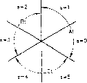
Fig. 4 is the space vector figure of explanation principle of the present invention.
Fig. 5 and 6 be explanation in each subregion of one-period, the schematic diagram of various parameters of the present invention.
Fig. 7 is the space vector figure that explanation is used for controlling according to the present invention the inequality of DC matrix.
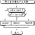
Fig. 8 is according to the present invention, is used for determining the simplification logical flow chart of the exemplary process of on-time.
Fig. 9-the 12nd illustrates the schematic diagram of each subregion in the cycle that can operate various switches therein.
Figure 13 is the logical flow chart (example of simplification) of non-vanishing vector switch option program.
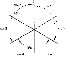
Figure 14 is the space vector figure that explanation is used to select the inequality of null vector.
Figure 15 is the simplification logical flow chart of exemplary null vector switch option program.
Figure 16 be the explanation principle of the invention, a series of waveforms on basis, common phase position.
Embodiment
With reference to Fig. 1, DC matrix converter 18 provides electric current to DC motor 19, and DC motor 19 mechanically is connected to pulley 20 in this embodiment, and pulley connects elevator cage 22 and balance weight 23 by rope 21.DC matrix converter 18 optionally is directly connected to each output j, the k of converter to three-phase AC power line a, b, c.Voltage may be at j end for just flowing to the k end, for example carry heavy duty when upwards being driven when elevator from the j end for negative and conventional forward current at the k end, perhaps the k end may for j end just for bearing and conventional forward current flows to j, for example carries underload when being driven downwards when elevator from k; This is called " motor driven ".No matter when elevator band underload moves up, is with heavy duty to move down or slows down, and 20 drive motors 19 that in fact slide make motor 19 play the effect of generator.In this case, it is opposite to flow through the polarity of voltage of polarity and j, k end of forward current of motor 19; This is called " regeneration ".DC matrix converter 18 understands according to the size and Orientation of the speed command of the DC matrix converter controller that offers Fig. 1 and motor 19 is operated under the motor driven mode or regeneration gets off suitably to connect each switch.
In the example herein, finally can cause the DC matrix converter to provide by conventional elevator running controller (not shown) with these orders of required mode drive motor 19, the latter provides speed command by circuit 30 to adder 31, and adder 31 deducts by 33 responses of rotine positioning and rate conversion circuit from the signal on the circuit 34 of the suitable conventional encoder (not shown) that is coupled with pulley 20 (or motor 19, decide with situation) and the actual speed that via line 32 provides.The output of the position of circuit 33 via line 37 is fed to the running controller so that determine to make elevator to move the continuity of necessary order in the mode of wanting, and these are well known in the art and do not constitute part of the present invention.Through holding wire 40 output of adder 31 is offered conventional speeds error ratio and storage gain circuit 41, the output of latter's via line 42 comprises the current order I that is fed to adder 43
*Adder 43 deducts actual motor current on the circuit 44 that obtains from conventional current detector 45 so that via line 46 provides current error signal.Handle current error signal with conventional ratio and storage gain in circuit 51, the output of the via line 52 of circuit 51 comprises voltage commands V
*
According to the present invention, the ratio decision modulation index m of the amplitude of the AC supply power voltage vector of the amplitude of voltage commands and input in fixing dg coordinate
*, the latter is used to determine duration of connecting between the pwm period of voltage on the AC input power line, so that obtain being used to be added in the required dc voltage on load such as the motor 19.
Voltage supply on AC power line a, b, the c is exported Vd, Vq to conventional fixedly three-phase to fixing dq coordinate transformation circuit 56 to provide, the latter as is known, in orthogonal coordinates, define the three-phase input voltage of AC power supplies.AC power supplies is in square root sum square of the amplitude V on the circuit 57 nothing but the Vd, the Vq that realize in conventional unit 58.Quadrature amplitude Vd, Vq also are fed to conventional phase-locked loop 63, and latter's via line 65 and 66 output are respectively the signals of reflection sin θ and cos θ.These signals are added on the circuit 68, and the latter is the modulation index m in the synchronous dq coordinate
*Convert modulation index component mq, md in the required fixedly dq coordinate to.Mq and md signal via line 71,72 are fed to duration and selection function piece 73, the latter determine selected switch to or group duration that should be switched on, and be chosen in switch that any given time will connect to or group, to carry out necessary pulse-width modulation, so that at the synthetic required dc voltage of output j, the k of DC matrix converter 18.Representation function piece 73 more fully below.Duration and each right signal of the selected switch that will connect that indication is connected offer timing circuit 78 through main line 77, and the latter in fact paired pulses carries out real-time counting so that provide the connection gate circuit to realize the required duration by the main line 79 through 12 lines to DC matrix converter 18.Timing circuit switches on and off each switch according to conventional commutation method, makes each output always be connected on the AC power line, and the gap of not opening circuit is so that satisfy known current continuity constraints.At the IEEETrans.Power Elec. in January, 1992, provided the example of a commutation in Holmes and Lipo " with the theoretical controlled rectifier of realizing of AC-AC matrix converter ".
Although not shown among Fig. 1, DC matrix converter of the present invention need be striden the line capacitance of AC input to support switch commutation hereinafter described.These electric capacity can be included in the input filter 82 together with the inductor of series connection.Similarly, the DC matrix converter preferably has the output filter 83 that comprises series inductance and shunt capacitance, and this two kinds of filters have been shown in aforementioned application.
An embodiment of explanation DC matrix converter 18 among Fig. 2.For each phase among AC power line a, b, the c, two power transistor switch on Fig. 2 top and two switches of Fig. 2 bottom are arranged.A switch on Fig. 2 top, at+, bt+, ct+ can be by the j end the conduct current motor 19 from a corresponding AC power line, and a meeting among corresponding lower switches ab+, bb+, the cb+ is from the corresponding AC power line of the conduct current of motor 19.Here in order to illustrate, suppose that from the j end be forward current through the electric current of motor 19 to k ends downwards.For reverse current, oppositely a meeting among lower switches ab-, bb-, the cb-from the electric current of a corresponding AC power line through k end, motor 19 guiding j ends, and a meeting among the top reverser at-, bt-, ct-is the corresponding AC power line of conduct current from the j end.
The general work characteristic of DC matrix converter is shown among Fig. 3.Wherein, draw sine voltage Va, Vb, the Vc of AC power line to the curve chart of time.A plurality of different current vector i1, i2...i6 that the various combination by conducting power transistor switch at+, bt+...cb-among Fig. 2 of also drawing among Fig. 3 draws.These are expressed as being pressed onto the vertical arrows that positive voltage extends from negative electricity.What interrelate with each vertical arrows is the horizontal arrow that has the same title in the bracket, it represents the part in each cycle, can the corresponding current vector of conversion in this section (in following example phase about 55 times) weekly so that no matter when input command is (m just
*>0) just produces positive voltage (Vj>Vk) at output.In each example, the top of arrow is designated as the electric current of the switch that indicates a, b or c of flowing through, and symbol At represents: perhaps transistor at+ or transistor at-can depend on that electric current is forward or reverse special time conducting as the aforementioned.Similarly, for current vector i1, symbol Cb represents transistor cb+, cb-is forward according to electric current for a moment or oppositely distinguishes conducting.Therefore, by respectively the AC power line of c phase and a AC power line mutually being connected to the k and the j end of matrix, obtain current vector i1 (as mentioned below, it is for forward or backwards).Current vector i1 can be present in point from Vc=0 in the time the point of Va=0.
The modulation index m that is used for the DC matrix converter of instruction
*Be converted into the following fixed space coordinate in the dq coordinate:
md=m*sinθ
mq=m*cosθ 0<θ<2π
Wherein θ=0 is corresponding to the q axle (63-68 among Fig. 1) of the AC power voltage line in the synchronous space coordinates.
Current i 1-i6 is the unique possibility that produces non-zero voltage (Vj is not equal to Vk) at output, can obtain these electric currents by two in the switch among a selection operation Fig. 2.For example, if switch at+ and switch bb+ in the while application drawing 2 can produce current i 6 as shown in Figure 3.If operate at+ and cb+ simultaneously, can produce the current i 1 of Fig. 3.If operate at+ and ab+ simultaneously, owing to do not produce different voltages (Vj=Vk) at output, the electric current that is defined as null vector here makes j, k terminal shortcircuit by at+ and the circulation of ab+ switch.Dc voltage synthetic is that the pulse-width modulation by (obtaining the minor system cycle thus as 100 μ s) under very high the frequency of AC power supplies relatively, the frequency as 10KHz realizes.At each 100 μ s in modulation period, first pair of switch (as At, Bb) meeting conducting in a certain section (being defined as " duty ratio " and " duration ") of modulation period, second pair of switch (as At, Cb) meeting conducting in a certain section of this modulation period, and by the one group of null vector that switch forms that relates to same phase place, as Bt, Bb can be in the remaining period conducting so that null vector to be provided, as described below.
With reference to Fig. 4, illustrate that the space vector figure of the method for control DC matrix converter comprises as the aforementioned, each the current vector li-i6 by selected switch is produced conducting.Current vector i1-i6 be separately six phase place subregion s=0 ... the boundary line of S=5.The leading boundary line of hysteresis boundary line that every boundary line is a phase place subregion and the next phase place subregion of following.Graphic extension produces (m under the positive output voltage condition among Fig. 4
*>0), modulation period, interior concrete torque current was with reference to i
*, this torque current is with reference on certain point that is present in the time that can utilize i6 and can utilize i1.This is defined as zero phase subregion (s=0).The modulation index m that obtains therefrom also is shown
*With correlative md, mq.For the modulation period of describing among Fig. 4, the leading current vector (or boundary line) that is defined as I α is current vector i6, and the lagging current vector (or boundary line) that is defined as I β is current vector i1.For near reference vector i
*, for corresponding current vector I α, I β, each sine value to the angle between the duty ratio of switch connection or duration d α, d β and reference vector and corresponding lead and lag current vector I α, the I β is directly proportional.The duty ratio that adopts in each subregion is provided by following equation:
dα=m*sin(π/3-φ) dβ=m*sin(φ) 0<φ<π/3
d0=1-dα-dβ
Wherein φ=0 and φ=π/3 correspond respectively to the position, angle of α vector sum β vector.
In addition, according to the present invention,, in following each subregion, utilize leg-of-mutton angle-and relation, measure with dq and to represent above-mentioned modulating function in order to determine the switch number of times.Use the fact of above-mentioned equation and φ=π/6+ θ-s π/3, wherein s is the subregion among Fig. 4, for 0<s<5, can express
dα=m*sin[π/3-(π/6+θ-sπ/3)]=m*sin(π/6+sπ/3-θ)
=m*sin(π/6+sπ/3)cosθ-m*cos(π/6+sπ/3)sinθ
=sin(π/6+sπ/3)mq-cos(π/6+sπ/3)md
And
dβ=m*sin(π/6+θ-sπ/3)=m*sin(π/6-sπ/3+θ)
=m*sin(π/6-sπ/3)cosθ+m*cos(π/6-sπ/3)sinθ
=sin(π/6-sπ/3)mq+cos(π/6-sπ/3)md
For reference, to s=5, in following table, provide sine and cosine coefficient value in the above equation for each subregion s=0.
| s | Sin(π/6+sπ/3) | -cos(π/6+sπ/3) | Sin(π/6-sπ/3) | cos(π/6-sπ/3) |
| 0 | 1/2 | -√3/2 | 1/2 | √3/2 |
| 1 | 1 | 0 | -1/2 | √3/2 |
| 2 | 1/2 | √3/2 | -1 | 0 |
| 3 | -1/2 | √3/2 | -1/2 | -√3/2 |
| 4 | -1 | 0 | 1/2 | -√3/2 |
| 5 | -1/2 | -√3/2 | 1 | 0 |
Respectively measure if definition is following like this:
m1= md- mq
m2= md+ mq
Then the amount that provides in by following table in each subregion of modulating function (α and β duty ratio) is determined:
| s | dα | dβ | |
| 0 | - | m2 | |
| 1 | | m1 | |
| 2 | m2 | - |
|
| 3 | m1 | -m2 | |
| 4 | -mq | -m1 |
| 5 | -m2 | mq |
This illustrates in the space vector figure of Fig. 5 and 6.Therefore, only determine that by amount mq, m1 and m2 this can easily calculate with aforesaid equation, shown in the step 101-104 among Fig. 8 for the duty cycle of two vectorial d α and d β on digital signal processor.
During the modulation period that subregion begins to locate, the switching time that is used for the α vector is very big, and it is very little to be used for switching time of β vector.In the centre of subregion, equal to be used for the switching time of β vector the switching time that is used for the α vector.Near the end of subregion, the turn-on time that is used for the β vector is very big and to be used for turn-on time of α vector very little.In the remainder of each modulation period, d0=1-d α-d β (duration that is used for null vector), connect like this relate to the pair of switches of same AC power line, as Bt, Bb so that null vector is provided, when utilizing minimum switch commutation number of times, adjust amplitude of output voltage thus.The time that different upper switches is connected in order to conduct vectorial α shown in Fig. 9, and the time that each upper switches is connected in order to conduct vectorial β shown in Figure 10.The time that different lower switches is connected in order to conduct vectorial α shown in Figure 11, and the time that each lower switches is connected in order to conduct vectorial β shown in Figure 12.When add (mq, m1 m2) with the condition that is defined as of AC power supplies input voltage vector place subregion, thisly determine it is by inequality test and test m to each amount
*Bear just and finish.Shown in Fig. 7 for m
*>0, the inequality of definition zone boundary.Here, Vd and Vq refer to the input AC power supplies voltage (Fig. 1,56) in fixed coordinates.For negative order (m
*>0), current vector I
*By from the radian of offset pi shown in Fig. 4.
The amount of α and β switch about following form is represented to be used to select.

Thereby before the test inequality, test 107 and step 108-111 are about m
*Symbol suitably define Vd ' and Vq '.As can be seen from Fig. 6, in by subregion 0 and 3 with the lower inequality definition | d β |=m2:
[Vd>-Vq/√3 ∩ Vd<Vq/√3]∪[Vd<-Vq/√3∩Vd>Vq/√3]
[|Vd|<Vq/√3]∪[|Vd|<-Vq/√3]
|Vd√3|<|Vq|
As shown in the test 115 of Fig. 8, this is to test easily on digital signal processor.Similarly, in subregion 1 and 4 by following inequality definition | d β |=m1:
[Vq<0∩Vd<Vq/√3]∪[Vq>0∩Vd>Vq/√3]
[VdVq>Vq
2/√3]∪[VdVq>Vq
2/√3]
VdVq√3>Vq
2
This determines in the test 116 of Fig. 8.
Remaining subregion 2 and 5 (wherein | d β |=mq) be to determine by get rid of handling (negative decision of test 115 and 116 among Fig. 8).Determine the sign of d β by the sign of test Vq in the test 117-119 of Fig. 8; If promptly Vq<0 then d β=-d β, as shown in the step 120-122 of Fig. 8.
Can easily draw duty ratio d α by noticing that duty ratio d α has been offset 2 π/3 radians with respect to the d β among Fig. 6 among Fig. 5.Therefore, by utilize following replacement when testing above-mentioned inequality, the definite and above-mentioned assignment of d α is consistent:
This is by the step of the step 123 of making replacement and 124 (Fig. 8) and repeating step and test 115-122 etc. and tests 125 and obtain.
Which in case be that α and β vector is determined turn-on time, must determine to connect switch to produce vector according to Fig. 4.This is the processing with two steps: be identified for the switch of non-vanishing vector, then be the null vector assigned switch.
Determine the phase place (being switch) that above-mentioned duty ratio or duration are used for according to the voltage vector region.For example, specify top mains switch in the DC matrix converter for α vector sum β vector shown in Fig. 9 and 10.If vector is arranged in one of subregion that indicates Bt, then assigned switch Bt.With reference to Figure 10, for switch Bt, can be jointly by test with lower inequality identification subregion s=1 or s=2 (test 130, Figure 13):
[Vd′>-Vq′/√3]∩[Vd′>Vq′/√3]
V d′√3>|Vq′|
For all the other upper switches of β vector appointment are after getting rid of subregion 1 and 2, determine by the sign of test Vq as shown in Figure 7; Vq '>0 if (test 131, certainly), then subregion be 0 or 5 and top β switch be At; Vq<0 if (test 131 is negated), then subregion is 3 or 4, and top β switch is Ct.
By in Fig. 9 careful with respect among Figure 10 about the phase shift of π/3 radians of the upper switches appointment of β vector, obtain easily specifying about the upper switches of α vector.Thus, if at first make following replacement, then about determine consistent with above-mentioned appointment (step 135 of Figure 13,136) of the upper switches of α vector:
Vd′=1/2Vd′-√3Vq′/2
Vq′=-1/2Vq′+√3 Vd′/2
These specify in shown in the test and step 138 of Figure 13.
About determining of the lower switches appointment of α vector sum β vector,, consistent with the above except about having between two groups the appointment the phase shift of π radian.Therefore, when using following replacement, described definite and above-mentioned consistent (step 140 of Figure 13,141):
Vd″=-Vd″
Vq″=-Vq″
Step at Figure 13 is made these selections with testing in 143.
As described above, null vector i0 is defined as output j, k by one group of homophase switch At, Ab; Bt, Bb; Ct, the Cb short circuit.Select which group switch to be used to represent that null vector influences the common mode output voltage.Applying of each vectorial i1-i6 causes each output j, k to be connected to one of AC power supplies voltage Va, Vb or Vc.The voltage difference that is added in supported V D two ends is the difference Vj-Vk of output phase voltage, and equals the quantity of two output line voltage sums divided by output phase with reference to the common-mode voltage VCM of the described system neutral line, i.e. (Vj+Vk)/2.Provide the gained difference and the common-mode voltage that produce by each vector in the following table:

| Vector | i0 | i0 | i0 |
| Switch | At,Ab | Bt,Bb | Ct,Cb |
| Vj | VA | VB | VC |
| Vk | VA | | VC |
| VD | |||
| 0 | 0 | 0 | |
| VCM | VA | VB | VC |
Because line voltage Va, Vb and Vc are sinusoidal, so can easily calculate the peak value common-mode voltage that draws at an AC in the cycle, by non-vanishing vector i1 to i6, following calculating:
VCM (peak value)=1/2 √ 2/3 VLL, 0<ω t≤2 π
Wherein VLL is the rms voltage between lines, and ω t is the AC phase angle of representing with radian.On the contrary, the peak value common-mode voltage that is obtained by null vector in same period is:
VCM (peak value)=√ 2/3 VLL, 0<ω t≤2 π
Therefore, to produce the peak value common-mode voltage be about non-vanishing vector two times for indiscriminate use null vector.
But, can select null vector so that reduce the peak value common-mode voltage with such method.For example, if null vector (At, use Ab) is limited to such cycle:
Wherein ω t=0 is corresponding to the peak value of line voltage Va, and maximum common mode voltage is given by following formula:

This is equivalent to

So, in the use of AC in the cycle, the peak value common-mode voltage of null vector generation has thus been reduced half by the restriction null vector.In order to realize this reduction factor, other null vectors are provided with same restriction to the whole AC cycle.This is summarized in the following table, and graphic extension in Figure 14.
| Null vector | The cycle that applies that allows |
| (At,Ab) | π/3<ω t<2 π/3 and 4 π/3<ω t<5 π/3 |
| (Bt,Bb) | 0<ω t<π/3 and π<ω t<4 π/3 |
| (Ct,Cb) | 2 π/3<ω t<π and 5 π/3<ω t<0 |
Be identified for the switches set of null vector, be expressed as SW0, what this was applicable to DC matrix converter middle and upper part and bottom respectively organizes switch.Determine which subregion voltage vector is positioned at and is tested by inequality and finish.The inequality of definition zone boundary is shown among Figure 14.Wherein these subregions of SW0=A are by defining with lower inequality (positive result of the test 139 of Figure 15):
Similarly, SW0=B discerns by testing following inequality (positive result of the test 140 of Figure 15):
SW0=C determines by exclusive method (negative decision of the test 140 of Figure 15).
If desired, can simplify procedures by being careful with the similarity that the algorithm of duty ratio is set, as long as make following replacement:
Vd=Vq
Vq=Vd
Select in the United States Patent (USP) NO.6166930 that literary composition is submitted to simultaneously therewith open and require its patent right with reference to Figure 14 and 15 at the null vector switch that preamble is described.
In each modulation period, each that is used for α vector, β vector and null vector is inessential to the operating sequence with each group switch.Therefore order can be α, β, zero; β, α, zero; β, zero, α; Perhaps any other order.Between one of one of AC power line and output the switch of conduction never disconnect, until another switch connection so that the AC power line to this end conducting, under such restrictive condition, switch shown in Fig. 4 (together with Fig. 9-12 and 14) shows with the relation of group (null vector) (α and β), by implementing the present invention, the switch commutation is minimized.For example, when the α vector is i6, connect switch At, and during the beat portion of each modulation period, keep connecting the right part of switch as being used for current vector i1 with its part (the leading boundary line that comprises phase place subregion s=0) as the α vector.On the other hand, in each modulation period in phase place subregion s=0, switch At can at first connect as the part of current vector i1 and keep the part of connection as current vector i6.Even and in a modulation period, α switch pair and β switch between operation null vector switches set, for example the At switch can be connected during the i6 of ending modulation period, and keeps connecting during the i1 of the beginning of the modulation period that the next one is followed.Therefore, under any circumstance, two switches were only connected once in each modulation period, with in any scheme of known before this prior art, each modulation period three switch connections situation differ widely.Therefore, in forming the process of non-vanishing vector, the used commutation number of times of switch reduced 1/3rd.There is same relation in commutation for null vector.
The benefit of the minimizing commutation that therefore, is provided by space vector method that represent among the space vector figure shown in Fig. 4, of the present invention can with null vector that illustrate, that allow by reduction among the described United States Patent (USP) NO.6166930 apply that common-mode voltage that the cycle realizes reducing provides, the requirement of the reduction of common mode magnetic cell is combined.Provide for m in the following table
*>0, the combined strategy of the vector of all permissions.
With reference to Fig. 4, the little phase angle φ place in subregion 0, in each pulse width modulation cycle, about α vector I6, switch At (together with switch Bb) connects the relatively long time, and about β vector I1, it connects the relatively short time (together with switch Cb).Opposite situation appears in the big phase angle φ place in the zero district.For the part that relates to α vector sum β vector simultaneously, switch At keeps connecting constantly.At the center of subregion 0, the At switch keeps the time maximum of connection, produces the duty cycle waveform of Figure 16 (a).Figure 16 (b) expression is for the logical time of the exemplary winding of switch at, bt and ct, and Figure 16 (c) illustrates (unfiltered, desirable) the instantaneous DC output voltage that will produce.
It is irrelevant with the present invention to carry out the order (Fig. 8,13 and 15) that calculates.Certainly, can operate in each modulation period should be to before maybe should the group switch, and it must be known that switch is selected the duration of (each to or group) and every pair or every group.The use of selection in timing circuit 78 and duration information is conventional, basically with the AC-AC matrix converter in use identical.
The present invention has been described in an embodiment, in this embodiment, have 12 switch at+, at-... cb+, cb-so that adapt to directly load with regeneration.But the present invention also can use in the DC matrix converter of the load that drives unidirectional nothing regeneration, for example is used to drive electric tool or other application scenarios.
Illustrated that the present invention can utilize n type, break-through, igbt power switch to realize.But the present invention can realize with the p transistor npn npn or with connecting into antiparallel nonpenetrated, igbt.
Claims (3)
1. one kind is passed through DC matrix converter (18) control DC load (19) and one group of three-phase AC power line (a, b, the method of the electric current c), described DC matrix converter comprises: each is connected a plurality of upper switches (at-between first DC output (J) of corresponding one and described DC matrix converter in the described AC power line, at+, bt-, bt+, ct-, ct+); And each be connected a plurality of lower switches between the 2nd DC output (K) of corresponding one and described DC matrix converter in the described AC power line (ab-, ab+, bb-, bb+, cb-, cb+), described method comprises:
Operate described switch by this way, make each switch work corresponding one when being connected to relevant specific of described DC output, maintenance work in the described AC power line and one of described AC power line is connected to described specific DC output until another switch being operated, and make one of described upper switches and one of described lower switches be simultaneously operated, described switch is operated (At, Cb in pairs; Bt, Cb; Bt, Ab; Ct, Ab; Ct, Bb; At, Bb), every pair comprises upper switches relevant with an AC power line and the AC power line relevant lower switches different with described that root AC power line, and described switch is also operated (Bt, Bb in groups; At, Ab; Ct, Cb), every group comprises upper switches and the lower switches relevant with same AC power line;
It is characterized in that:
Voltage command signal V is provided
*(52), its expression is offered the voltage of described load by described DC output;
(53) modulation index m is provided
*, it is described voltage command signal V
*With the fixing ratio of the instantaneous amplitude V (57) of the voltage of AC power line described in d, the q coordinate; And
In-phase modulation exponential component mq=m is provided
*Cos θ (71,102) and quadrature modulation exponential component md=m
*Sin θ (72,101);
(73) amount is provided
The amount of providing
(56) instantaneous AC power voltage line in-phase component Vq and quadrature component Vd in quadrature coordinate consistent with the phase place of given (a) in the described AC power line is provided, and
When
(115) time, if if Vq>0 would provide the d α of first=-m1 Vq<0 then d is provided α=m1, and if Vq>0 (119) then second portion (115) is provided if d β=m2 Vq<0 then provide d β=-m2;
When
(116) time, if Vq>0 if the described d of first α=mq Vq<0 would be provided provide d α=-mq, and if Vq>0 then described second portion d β=m1 (116) is provided if Vq<0 (117) would provide d β=-m1, and
Non-at once
, also non-
(116) time, if if Vq>0 would provide the described d α of first=-m2 Vq<0 then d α=m2, and if Vq>0 then if described second portion d β=mq Vq<0 (118) is provided then provide d β=-mq, and
In each cycle of the continuous sequence of comparing the modulation period of wanting littler with the cycle of described AC power supplies voltage, first pair of switch in the described switch of the described d α of first manipulate in described cycle, second pair of switch in the described switch of described second portion d β manipulate in described cycle, and at one group of switch of remainder manipulate in described cycle.
2. the method for claim 1 is characterized in that: in described modulation period, the described first time is prior to the described second portion time.
3. the method for claim 1 is characterized in that: in described modulation period, the described remainder in described cycle follows after described first and second part-times.
Applications Claiming Priority (2)
| Application Number | Priority Date | Filing Date | Title |
|---|---|---|---|
| US09/310,393 | 1999-05-12 | ||
| US09/310,393 US6058028A (en) | 1999-05-12 | 1999-05-12 | Control of a DC matrix converter |
Publications (2)
| Publication Number | Publication Date |
|---|---|
| CN1350719A CN1350719A (en) | 2002-05-22 |
| CN100392975C true CN100392975C (en) | 2008-06-04 |
Family
ID=23202300
Family Applications (1)
| Application Number | Title | Priority Date | Filing Date |
|---|---|---|---|
| CNB008074933A Expired - Fee Related CN100392975C (en) | 1999-05-12 | 2000-05-04 | Control of a DC matrix converter |
Country Status (7)
| Country | Link |
|---|---|
| US (1) | US6058028A (en) |
| EP (1) | EP1177615B1 (en) |
| JP (1) | JP4499300B2 (en) |
| CN (1) | CN100392975C (en) |
| DE (1) | DE60001275T2 (en) |
| HK (1) | HK1046592B (en) |
| WO (1) | WO2000070734A1 (en) |
Cited By (1)
| Publication number | Priority date | Publication date | Assignee | Title |
|---|---|---|---|---|
| US9859816B2 (en) | 2015-11-17 | 2018-01-02 | Delta Electronics (Shanghai) Co., Ltd. | Method for controlling modulation wave and three-phase three-wire three-level circuit |
Families Citing this family (29)
| Publication number | Priority date | Publication date | Assignee | Title |
|---|---|---|---|---|
| US6163472A (en) * | 1999-05-12 | 2000-12-19 | Otis Elevator Company | Elevator DC motor drive with unity power factor, including regeneration |
| US6137703A (en) * | 1999-11-23 | 2000-10-24 | Otis Elevator Company | Clamped bidirectional power switches |
| DE10039957A1 (en) * | 2000-08-16 | 2002-03-07 | Siemens Ag | Device for basic interference suppression of a matrix converter |
| DE10051222A1 (en) * | 2000-10-16 | 2002-04-25 | Alstom Switzerland Ltd | Method for operating a matrix converter and matrix converter for performing the method |
| DE10135337A1 (en) * | 2001-07-19 | 2003-02-06 | Siemens Ag | Method and device for stopping a drive with a matrix converter in the event of a power failure |
| GB0208600D0 (en) * | 2002-04-15 | 2002-05-22 | Nottingham University | Power converter |
| EP1434339A3 (en) * | 2002-12-24 | 2004-10-06 | Becromal S.p.A. | Circuit for power supply |
| JP2005137076A (en) * | 2003-10-29 | 2005-05-26 | Favess Co Ltd | Apparatus and method for controlling motor |
| EP1788911B1 (en) * | 2004-08-19 | 2017-06-28 | Otis Elevator Company | Operating a three phase device using single phase power |
| CN100568698C (en) * | 2005-09-09 | 2009-12-09 | 张长安 | A kind of digital control method that is used for inverter and DC frequency-changing |
| JP2007082321A (en) * | 2005-09-14 | 2007-03-29 | Fuji Electric Fa Components & Systems Co Ltd | Motor drive unit |
| CN100362736C (en) * | 2005-09-15 | 2008-01-16 | 上海交通大学 | Combined two-way power switch with capacitance clamping circuit |
| CN100394685C (en) * | 2005-09-15 | 2008-06-11 | 上海交通大学 | Combined two-way power switch with diode clamping circuit |
| CN101257279B (en) * | 2007-03-01 | 2010-05-26 | 富士电机系统株式会社 | Motor drive device |
| CN101675580B (en) * | 2007-05-16 | 2013-03-27 | 奥蒂斯电梯公司 | Pulse width modulation control of a matrix converter |
| CN100557943C (en) * | 2008-06-13 | 2009-11-04 | 株洲南车时代电气股份有限公司 | A kind of synchronous modulation method based on space vector |
| KR101095900B1 (en) | 2009-08-05 | 2011-12-21 | 울산대학교 산학협력단 | Space vector modulation method of matrix converter and system thereof |
| CN101741257B (en) * | 2009-12-24 | 2012-05-09 | 合肥工业大学 | Control system for restraining common-mode voltage of dual stage matrix converter |
| RU2444833C1 (en) * | 2010-06-30 | 2012-03-10 | Государственное образовательное учреждение высшего профессионального образования "Новосибирский государственный технический университет" | Vector method for control of three-phase static converter with asymmetric load |
| US9154126B2 (en) * | 2010-10-14 | 2015-10-06 | Nxp B.V. | High voltage output driver |
| US20120091985A1 (en) * | 2010-10-14 | 2012-04-19 | Pieter Gustaaf Nierop | High Voltage Output Driver |
| FR2975843B1 (en) * | 2011-05-23 | 2013-05-17 | Renault Sa | METHOD FOR CONTROLLING THE SWITCHES OF A CURRENT RECTIFIER CONNECTED TO AN ONBOARD CHARGER. |
| US9793352B1 (en) | 2011-06-02 | 2017-10-17 | Ixys Corporation | IGBT assembly having saturable inductor for soft landing a diode recovery current |
| CN102545665B (en) * | 2012-02-09 | 2013-12-25 | 天津大学 | Three-level PWM (Pulse-Width Modulation) rectifier direct power control method |
| WO2014020703A1 (en) * | 2012-07-31 | 2014-02-06 | 株式会社安川電機 | Matrix converter |
| CN103138599B (en) * | 2013-02-25 | 2014-12-10 | 南京航空航天大学 | Operational control method for two-stage matrix converter |
| WO2018183595A1 (en) * | 2017-03-31 | 2018-10-04 | Murata Manufacturing Co., Ltd. | Apparatus and method of operating matrix converter-based rectifier when one phase is disconnected or is short-circuited |
| US11290023B2 (en) * | 2019-04-11 | 2022-03-29 | Hamilton Sundstrand Corporation | Model predictive control for matrix converter operating in current control mode with load current estimation |
| CN110401355B (en) * | 2019-07-31 | 2020-12-22 | 河北工业大学 | Indirect matrix converter modulation method for inhibiting common-mode voltage |
Citations (5)
| Publication number | Priority date | Publication date | Assignee | Title |
|---|---|---|---|---|
| SU570618A1 (en) * | 1975-02-27 | 1977-08-30 | Отделение ордена Ленина института химической физики АН СССР | Method of preparing dyed polyolefines |
| US4599685A (en) * | 1984-01-25 | 1986-07-08 | Hitachi, Ltd. | Control circuit for power converter apparatus |
| US4984147A (en) * | 1989-05-12 | 1991-01-08 | Mitsubishi Denki Kabushiki Kaisah | Control method for PWM converter |
| US5153821A (en) * | 1991-09-06 | 1992-10-06 | Otis Elevator Company | Pulse-width-modulation method for providing extended linearity, reduced commutation losses and increase in inverter/converter output voltage |
| US5852551A (en) * | 1996-10-02 | 1998-12-22 | Lg Industrial Systems Co., Ltd. | Pulsed width modulation method for power transforming apparatus |
Family Cites Families (5)
| Publication number | Priority date | Publication date | Assignee | Title |
|---|---|---|---|---|
| US3961154A (en) * | 1972-04-18 | 1976-06-01 | Elektriska Svetsningsaktiebolaget | Direct current power supply for manual arc welding |
| US5541827A (en) * | 1995-05-17 | 1996-07-30 | Doble Engineering Company | Reducing switching losses in a phase-modulated switch-mode amplifier |
| US5706186A (en) * | 1996-09-23 | 1998-01-06 | Allen-Bradley Company, Inc. | Hybrid pulse width modulation method and apparatus |
| JP3518978B2 (en) * | 1997-08-25 | 2004-04-12 | 東洋電機製造株式会社 | Converter control device for obtaining DC from polyphase AC |
| JPH11122944A (en) * | 1997-10-15 | 1999-04-30 | Toshiba Corp | Controller of npc converter |
-
1999
- 1999-05-12 US US09/310,393 patent/US6058028A/en not_active Ceased
-
2000
- 2000-05-04 DE DE60001275T patent/DE60001275T2/en not_active Expired - Lifetime
- 2000-05-04 CN CNB008074933A patent/CN100392975C/en not_active Expired - Fee Related
- 2000-05-04 EP EP00930358A patent/EP1177615B1/en not_active Expired - Lifetime
- 2000-05-04 WO PCT/US2000/012149 patent/WO2000070734A1/en active IP Right Grant
- 2000-05-04 JP JP2000619077A patent/JP4499300B2/en not_active Expired - Fee Related
-
2002
- 2002-11-07 HK HK02108086.6A patent/HK1046592B/en not_active IP Right Cessation
Patent Citations (5)
| Publication number | Priority date | Publication date | Assignee | Title |
|---|---|---|---|---|
| SU570618A1 (en) * | 1975-02-27 | 1977-08-30 | Отделение ордена Ленина института химической физики АН СССР | Method of preparing dyed polyolefines |
| US4599685A (en) * | 1984-01-25 | 1986-07-08 | Hitachi, Ltd. | Control circuit for power converter apparatus |
| US4984147A (en) * | 1989-05-12 | 1991-01-08 | Mitsubishi Denki Kabushiki Kaisah | Control method for PWM converter |
| US5153821A (en) * | 1991-09-06 | 1992-10-06 | Otis Elevator Company | Pulse-width-modulation method for providing extended linearity, reduced commutation losses and increase in inverter/converter output voltage |
| US5852551A (en) * | 1996-10-02 | 1998-12-22 | Lg Industrial Systems Co., Ltd. | Pulsed width modulation method for power transforming apparatus |
Cited By (1)
| Publication number | Priority date | Publication date | Assignee | Title |
|---|---|---|---|---|
| US9859816B2 (en) | 2015-11-17 | 2018-01-02 | Delta Electronics (Shanghai) Co., Ltd. | Method for controlling modulation wave and three-phase three-wire three-level circuit |
Also Published As
| Publication number | Publication date |
|---|---|
| JP2003500988A (en) | 2003-01-07 |
| WO2000070734A1 (en) | 2000-11-23 |
| EP1177615B1 (en) | 2003-01-22 |
| CN1350719A (en) | 2002-05-22 |
| JP4499300B2 (en) | 2010-07-07 |
| HK1046592B (en) | 2009-05-22 |
| EP1177615A1 (en) | 2002-02-06 |
| US6058028A (en) | 2000-05-02 |
| DE60001275T2 (en) | 2004-01-22 |
| HK1046592A1 (en) | 2003-01-17 |
| DE60001275D1 (en) | 2003-02-27 |
Similar Documents
| Publication | Publication Date | Title |
|---|---|---|
| CN100392975C (en) | Control of a DC matrix converter | |
| Novotny et al. | Vector control and dynamics of AC drives | |
| US6166930A (en) | Reduced common voltage in a DC matrix converter | |
| USRE38439E1 (en) | Control of a DC matrix converter | |
| US6320775B1 (en) | Power conversion apparatus utilizing zero-phase power supply device that provides zero-phase sequence components | |
| Rivera et al. | Imposed sinusoidal source and load currents for an indirect matrix converter | |
| CN107210702B (en) | Power conversion device | |
| CN101771380B (en) | Space vector modulation method for inverter directly controlled by torque | |
| CN101145754A (en) | Current detecting unit and motor control device | |
| CN101154917B (en) | Method and apparatus for PWM control of voltage source inverter to minimize current sampling errors in electric drives | |
| CN108054913B (en) | PFC circuit, motor control system and variable frequency air conditioner | |
| CN103107761B (en) | Three-dimensional space vector pulse width modulation (SVPWM) method based on four-phrase five-wire topology | |
| Chen et al. | A novel simplified space-vector-modulated control scheme for three-phase switch-mode rectifier | |
| CN105917549A (en) | Split phase power conversion apparatuses, methods and systems | |
| CN110022103A (en) | A kind of Direct Torque Control device and method of direct current biasing sinusoidal current motor | |
| Kozakevich | Investigation of the direct torque control system of an electromechanical system with a matrix converter | |
| CN107466441A (en) | The control device of inverter | |
| CN109873593A (en) | A kind of six-phase motor space vector modulating method, device and its application | |
| KR101889480B1 (en) | Driving device for dual parallel motors | |
| Fischer et al. | Investigation on Carrier Signals to Minimize the Overall Current Ripple of an Interleaved-Switched Inverter | |
| Zidani et al. | Improvement of the indirect field oriented control for IM drives using fuzzy controllers | |
| JP2022080081A (en) | Switching power source apparatus, and control device and control method therefor | |
| CN102739088A (en) | Multi-phase voltage source two-level inverter control method | |
| Patra | Study of induction motor drive with direct torque control scheme and indirect field oriented control scheme using space vector modulation | |
| Soebagia et al. | Input power factor control of AC-DC series resonant DC link converter using PID operation |
Legal Events
| Date | Code | Title | Description |
|---|---|---|---|
| C06 | Publication | ||
| PB01 | Publication | ||
| C10 | Entry into substantive examination | ||
| SE01 | Entry into force of request for substantive examination | ||
| C14 | Grant of patent or utility model | ||
| GR01 | Patent grant | ||
| REG | Reference to a national code |
Ref country code: HK Ref legal event code: GR Ref document number: 1046592 Country of ref document: HK |
|
| CF01 | Termination of patent right due to non-payment of annual fee |
Granted publication date: 20080604 Termination date: 20150504 |
|
| EXPY | Termination of patent right or utility model |