BR112017013680B1 - OPTICAL SYSTEM - Google Patents
OPTICAL SYSTEM Download PDFInfo
- Publication number
- BR112017013680B1 BR112017013680B1 BR112017013680-5A BR112017013680A BR112017013680B1 BR 112017013680 B1 BR112017013680 B1 BR 112017013680B1 BR 112017013680 A BR112017013680 A BR 112017013680A BR 112017013680 B1 BR112017013680 B1 BR 112017013680B1
- Authority
- BR
- Brazil
- Prior art keywords
- substrate
- optical system
- light waves
- transparent layer
- optical
- Prior art date
Links
- 230000003287 optical effect Effects 0.000 title claims abstract description 77
- 239000000758 substrate Substances 0.000 claims abstract description 86
- 230000008878 coupling Effects 0.000 claims abstract description 21
- 238000010168 coupling process Methods 0.000 claims abstract description 21
- 238000005859 coupling reaction Methods 0.000 claims abstract description 21
- 238000000576 coating method Methods 0.000 claims description 19
- 239000011248 coating agent Substances 0.000 claims description 18
- 239000000463 material Substances 0.000 claims description 11
- 238000000034 method Methods 0.000 claims description 11
- 239000006117 anti-reflective coating Substances 0.000 claims description 8
- 239000000853 adhesive Substances 0.000 claims description 7
- 230000001070 adhesive effect Effects 0.000 claims description 7
- 239000003989 dielectric material Substances 0.000 claims description 7
- 239000007787 solid Substances 0.000 claims description 6
- 230000008021 deposition Effects 0.000 claims description 2
- 230000003667 anti-reflective effect Effects 0.000 claims 1
- 239000010410 layer Substances 0.000 description 7
- 230000000717 retained effect Effects 0.000 description 5
- 238000004519 manufacturing process Methods 0.000 description 4
- 238000010586 diagram Methods 0.000 description 3
- 230000004424 eye movement Effects 0.000 description 3
- 239000012790 adhesive layer Substances 0.000 description 2
- 239000004568 cement Substances 0.000 description 2
- 230000009977 dual effect Effects 0.000 description 2
- 238000005516 engineering process Methods 0.000 description 2
- 238000003384 imaging method Methods 0.000 description 2
- 210000001747 pupil Anatomy 0.000 description 2
- 238000001228 spectrum Methods 0.000 description 2
- 239000010409 thin film Substances 0.000 description 2
- 201000009310 astigmatism Diseases 0.000 description 1
- 238000005452 bending Methods 0.000 description 1
- 230000003247 decreasing effect Effects 0.000 description 1
- 239000000835 fiber Substances 0.000 description 1
- 239000004973 liquid crystal related substance Substances 0.000 description 1
- 239000002991 molded plastic Substances 0.000 description 1
- 208000001491 myopia Diseases 0.000 description 1
- 230000004379 myopia Effects 0.000 description 1
- ORQBXQOJMQIAOY-UHFFFAOYSA-N nobelium Chemical compound [No] ORQBXQOJMQIAOY-UHFFFAOYSA-N 0.000 description 1
- 230000001681 protective effect Effects 0.000 description 1
Images


Classifications
-
- G—PHYSICS
- G02—OPTICS
- G02B—OPTICAL ELEMENTS, SYSTEMS OR APPARATUS
- G02B27/00—Optical systems or apparatus not provided for by any of the groups G02B1/00 - G02B26/00, G02B30/00
- G02B27/0081—Optical systems or apparatus not provided for by any of the groups G02B1/00 - G02B26/00, G02B30/00 with means for altering, e.g. enlarging, the entrance or exit pupil
-
- G—PHYSICS
- G02—OPTICS
- G02B—OPTICAL ELEMENTS, SYSTEMS OR APPARATUS
- G02B27/00—Optical systems or apparatus not provided for by any of the groups G02B1/00 - G02B26/00, G02B30/00
- G02B27/01—Head-up displays
-
- G—PHYSICS
- G02—OPTICS
- G02B—OPTICAL ELEMENTS, SYSTEMS OR APPARATUS
- G02B27/00—Optical systems or apparatus not provided for by any of the groups G02B1/00 - G02B26/00, G02B30/00
- G02B27/01—Head-up displays
- G02B27/0101—Head-up displays characterised by optical features
-
- G—PHYSICS
- G02—OPTICS
- G02B—OPTICAL ELEMENTS, SYSTEMS OR APPARATUS
- G02B27/00—Optical systems or apparatus not provided for by any of the groups G02B1/00 - G02B26/00, G02B30/00
- G02B27/01—Head-up displays
- G02B27/017—Head mounted
- G02B27/0172—Head mounted characterised by optical features
-
- G—PHYSICS
- G02—OPTICS
- G02B—OPTICAL ELEMENTS, SYSTEMS OR APPARATUS
- G02B27/00—Optical systems or apparatus not provided for by any of the groups G02B1/00 - G02B26/00, G02B30/00
- G02B27/01—Head-up displays
- G02B27/017—Head mounted
- G02B27/0176—Head mounted characterised by mechanical features
-
- G—PHYSICS
- G02—OPTICS
- G02B—OPTICAL ELEMENTS, SYSTEMS OR APPARATUS
- G02B27/00—Optical systems or apparatus not provided for by any of the groups G02B1/00 - G02B26/00, G02B30/00
- G02B27/10—Beam splitting or combining systems
- G02B27/14—Beam splitting or combining systems operating by reflection only
-
- G—PHYSICS
- G02—OPTICS
- G02B—OPTICAL ELEMENTS, SYSTEMS OR APPARATUS
- G02B27/00—Optical systems or apparatus not provided for by any of the groups G02B1/00 - G02B26/00, G02B30/00
- G02B27/42—Diffraction optics, i.e. systems including a diffractive element being designed for providing a diffractive effect
- G02B27/4205—Diffraction optics, i.e. systems including a diffractive element being designed for providing a diffractive effect having a diffractive optical element [DOE] contributing to image formation, e.g. whereby modulation transfer function MTF or optical aberrations are relevant
-
- G—PHYSICS
- G02—OPTICS
- G02B—OPTICAL ELEMENTS, SYSTEMS OR APPARATUS
- G02B6/00—Light guides; Structural details of arrangements comprising light guides and other optical elements, e.g. couplings
- G02B6/0001—Light guides; Structural details of arrangements comprising light guides and other optical elements, e.g. couplings specially adapted for lighting devices or systems
- G02B6/0011—Light guides; Structural details of arrangements comprising light guides and other optical elements, e.g. couplings specially adapted for lighting devices or systems the light guides being planar or of plate-like form
- G02B6/0013—Means for improving the coupling-in of light from the light source into the light guide
- G02B6/0023—Means for improving the coupling-in of light from the light source into the light guide provided by one optical element, or plurality thereof, placed between the light guide and the light source, or around the light source
- G02B6/0031—Reflecting element, sheet or layer
-
- G—PHYSICS
- G02—OPTICS
- G02B—OPTICAL ELEMENTS, SYSTEMS OR APPARATUS
- G02B6/00—Light guides; Structural details of arrangements comprising light guides and other optical elements, e.g. couplings
- G02B6/0001—Light guides; Structural details of arrangements comprising light guides and other optical elements, e.g. couplings specially adapted for lighting devices or systems
- G02B6/0011—Light guides; Structural details of arrangements comprising light guides and other optical elements, e.g. couplings specially adapted for lighting devices or systems the light guides being planar or of plate-like form
- G02B6/0033—Means for improving the coupling-out of light from the light guide
- G02B6/0035—Means for improving the coupling-out of light from the light guide provided on the surface of the light guide or in the bulk of it
-
- G—PHYSICS
- G02—OPTICS
- G02B—OPTICAL ELEMENTS, SYSTEMS OR APPARATUS
- G02B6/00—Light guides; Structural details of arrangements comprising light guides and other optical elements, e.g. couplings
- G02B6/0001—Light guides; Structural details of arrangements comprising light guides and other optical elements, e.g. couplings specially adapted for lighting devices or systems
- G02B6/0011—Light guides; Structural details of arrangements comprising light guides and other optical elements, e.g. couplings specially adapted for lighting devices or systems the light guides being planar or of plate-like form
- G02B6/0033—Means for improving the coupling-out of light from the light guide
- G02B6/005—Means for improving the coupling-out of light from the light guide provided by one optical element, or plurality thereof, placed on the light output side of the light guide
-
- G—PHYSICS
- G02—OPTICS
- G02B—OPTICAL ELEMENTS, SYSTEMS OR APPARATUS
- G02B6/00—Light guides; Structural details of arrangements comprising light guides and other optical elements, e.g. couplings
- G02B6/0001—Light guides; Structural details of arrangements comprising light guides and other optical elements, e.g. couplings specially adapted for lighting devices or systems
- G02B6/0011—Light guides; Structural details of arrangements comprising light guides and other optical elements, e.g. couplings specially adapted for lighting devices or systems the light guides being planar or of plate-like form
- G02B6/0065—Manufacturing aspects; Material aspects
-
- G—PHYSICS
- G02—OPTICS
- G02B—OPTICAL ELEMENTS, SYSTEMS OR APPARATUS
- G02B1/00—Optical elements characterised by the material of which they are made; Optical coatings for optical elements
- G02B1/10—Optical coatings produced by application to, or surface treatment of, optical elements
- G02B1/11—Anti-reflection coatings
-
- G—PHYSICS
- G02—OPTICS
- G02B—OPTICAL ELEMENTS, SYSTEMS OR APPARATUS
- G02B27/00—Optical systems or apparatus not provided for by any of the groups G02B1/00 - G02B26/00, G02B30/00
- G02B27/01—Head-up displays
- G02B27/0101—Head-up displays characterised by optical features
- G02B2027/0123—Head-up displays characterised by optical features comprising devices increasing the field of view
- G02B2027/0125—Field-of-view increase by wavefront division
-
- G—PHYSICS
- G02—OPTICS
- G02B—OPTICAL ELEMENTS, SYSTEMS OR APPARATUS
- G02B27/00—Optical systems or apparatus not provided for by any of the groups G02B1/00 - G02B26/00, G02B30/00
- G02B27/01—Head-up displays
- G02B27/0149—Head-up displays characterised by mechanical features
- G02B2027/015—Head-up displays characterised by mechanical features involving arrangement aiming to get less bulky devices
-
- G—PHYSICS
- G02—OPTICS
- G02B—OPTICAL ELEMENTS, SYSTEMS OR APPARATUS
- G02B27/00—Optical systems or apparatus not provided for by any of the groups G02B1/00 - G02B26/00, G02B30/00
- G02B27/01—Head-up displays
- G02B27/017—Head mounted
- G02B2027/0178—Eyeglass type
-
- G—PHYSICS
- G02—OPTICS
- G02B—OPTICAL ELEMENTS, SYSTEMS OR APPARATUS
- G02B6/00—Light guides; Structural details of arrangements comprising light guides and other optical elements, e.g. couplings
- G02B6/0001—Light guides; Structural details of arrangements comprising light guides and other optical elements, e.g. couplings specially adapted for lighting devices or systems
- G02B6/0011—Light guides; Structural details of arrangements comprising light guides and other optical elements, e.g. couplings specially adapted for lighting devices or systems the light guides being planar or of plate-like form
- G02B6/0013—Means for improving the coupling-in of light from the light source into the light guide
- G02B6/0015—Means for improving the coupling-in of light from the light source into the light guide provided on the surface of the light guide or in the bulk of it
Abstract
Um sistema óptico inclui um substrato transmissor de luz tendo pelo menos duas superfícies e bordas principais externas e um elemento óptico para acoplamento de ondas de luz dentro do substrato, por reflexão interna total. Pelo menos uma superfície refletiva parcial está localizada no substrato para acoplamento de ondas de luz fora do substrato e, pelo menos, uma camada transparente, tendo um índice refrativo substancialmente menor do que o índice refrativo do substrato de transmissão de luz é opticamente anexada a pelo menos uma das superfícies principais do substrato, definindo um plano de interface. As ondas de luz acopladas dentro do substrato são, de forma total e substancial, refletidas a partir do plano de interface entre a superfície principal do substrato e a camada transparente.An optical system includes a light transmitting substrate having at least two outer leading surfaces and edges and an optical element for coupling light waves within the substrate by total internal reflection. At least one partial reflective surface is located on the substrate for coupling light waves off the substrate, and at least one transparent layer having a refractive index substantially lower than the refractive index of the light transmitting substrate is optically attached to at least one least one of the main surfaces of the substrate, defining an interface plane. The light waves coupled within the substrate are fully and substantially reflected from the interface plane between the main surface of the substrate and the transparent layer.
Description
[0001] A presente invenção refere-se a dispositivos ópticos de substrato guiado e, particularmente, a dispositivos que incluem uma pluralidade de superfícies refletivas carregadas através de um substrato transmissor de luz comum, também referido como um elemento de guia de luz. Antecedentes da invenção[0001] The present invention relates to guided substrate optical devices, and particularly devices that include a plurality of reflective surfaces charged through a common light transmitting substrate, also referred to as a light guiding element. Background of the invention
[0002] Uma aplicação importante para os elementos ópticos compactos é em mostradores montados na cabeça (HMDs), onde um módulo ótico serve tanto como uma lente de imagem e um combinador, onde uma fonte de imagem bidimensional é representada por imagem ao infinito e refletida dentro do olho de um observador. A fonte de exibição pode ser diretamente obtida a partir de tanto um modulador de luz espacial (SLM), tal como um tubo de raios catódicos (CRT), um mostrador de cristal líquido (LCD), um conjunto de diodos emissores de luz orgânicos (OLED), uma fonte de varrimento ou dispositivos semelhantes, ou indiretamente, por meio de uma relay lens ou um feixe de fibras ópticas. A fonte de exibição compreende um conjunto de elementos (pixels), representado ao infinito por uma lente de colimação, e é transmitida para o olho do observador por meio de uma superfície refletora, ou parcialmente refletora, atuando como um combinador para aplicações de visualização transparente e não transparente, respectivamente. Tipicamente, um módulo óptico livre de espaço convencional é usado para estes fins. No entanto, conforme o campo de visão (FOV) desejado do sistema aumenta, tal módulo óptico convencional torna-se maior, mais pesado e mais volumoso e, consequentemente, mesmo para um dispositivo de desempenho moderado tal como um sistema, é impraticável. Esta é uma grande desvantagem para todos os tipos de mostradores e, especialmente em aplicações montadas na cabeça, onde o sistema deve ser necessariamente o mais leve e o mais compacto possível.[0002] An important application for compact optical elements is in head-mounted displays (HMDs), where an optical module serves as both an imaging lens and a combiner, where a two-dimensional image source is imaged to infinity and reflected. within the eye of an observer. The display source can be directly obtained from either a spatial light modulator (SLM), such as a cathode ray tube (CRT), a liquid crystal display (LCD), an array of organic light-emitting diodes ( OLED), a scanning source or similar devices, or indirectly through a relay lens or fiber optic bundle. The display source comprises a set of elements (pixels), represented to infinity by a collimation lens, and is transmitted to the observer's eye through a reflective or partially reflective surface, acting as a combiner for transparent viewing applications. and non-transparent, respectively. Typically, a conventional space-free optical module is used for these purposes. However, as the desired field of view (FOV) of the system increases, such a conventional optical module becomes larger, heavier, and bulkier, and consequently, even for a moderately performing device such as a system, is impractical. This is a major disadvantage for all types of dials, and especially in head-mounted applications, where the system must necessarily be as light and compact as possible.
[0003] O esforço para compacidade levou a várias soluções ópticas complexas diferentes todas as quais, por um lado, ainda não são suficientemente compactas para a maioria das aplicações práticas, e por outro lado, sofrem grandes desvantagens em termos de fabricação. Além disso, a caixa de movimento ocular (EMB) dos ângulos de visualização ópticos resultantes desses modelos é normalmente muito pequena, tipicamente inferior a 8 mm. Assim, o desempenho do sistema óptico é muito sensível, mesmo para pequenos movimentos do sistema óptico em relação ao olho do observador e não permitindo o movimento suficiente da pupila para a leitura confortável de textos a partir de tais mostradores.[0003] The drive for compactness has led to several different complex optical solutions all of which, on the one hand, are still not compact enough for most practical applications, and on the other hand, suffer from major manufacturing disadvantages. Additionally, the eye movement box (EMB) of optical viewing angles resulting from these models is typically very small, typically less than 8mm. Thus, the performance of the optical system is very sensitive, even for small movements of the optical system in relation to the eye of the observer and not allowing sufficient pupil movement for comfortable reading of texts from such dials.
[0004] Os ensinamentos incluídos nas Publicações Nos. WO 01/95027, WO 03/081320, WO 2005/024485, WO 2005/024491, WO 2005/024969, WO 2005/124427, WO 2006/013565, WO 2006/085309, WO 2006/085310, WO 2006/087709, WO 2007/054928, WO 2007/093983, WO 2008/023367, WO 2008/129539, WO 2008/149339, WO 2013/175465, IL 232197 e IL 235642, todas em nome da Requerente, são aqui incorporados por referência.[0004] The teachings included in Publications Nos. WO 01/95027 , WO 03/081320 , WO 2005/024485 , WO 2005/024491 , WO 2005/024969 , WO 2005/124427 , WO 2006/013565 , WO 2006/085309 , WO 2006/085310 , WO 20706 WO 2007/054928 , WO 2007/093983 , WO 2008/023367 , WO 2008/129539 , WO 2008/149339 , WO 2013/175465 , IL 232197 and IL 235642 , all on behalf of the Applicant, are incorporated herein by reference.
[0005] A presente invenção facilita a exploração de um elemento óptico de guia luz (LOE) muito compacto para, entre outras aplicações, os HMDs. A invenção permite FOVs relativamente largos junto com valores de EMB relativamente grandes. O sistema óptico resultante oferece uma imagem grande, de alta qualidade, que também acomoda grandes movimentos do olho. O sistema óptico oferecido pela presente invenção é particularmente vantajoso porque é substancialmente mais compacto do que as implementações do estado da técnica e ainda, pode ser facilmente incorporado, mesmo em sistemas ópticos tendo configurações especializadas.[0005] The present invention facilitates the exploitation of a very compact light guide optical element (LOE) for, among other applications, HMDs. The invention allows for relatively large FOVs along with relatively large EMB values. The resulting optical system delivers a large, high-quality image that also accommodates large eye movements. The optical system offered by the present invention is particularly advantageous because it is substantially more compact than state-of-the-art implementations and further, can be easily incorporated, even in optical systems having specialized configurations.
[0006] Um amplo objetivo da presente invenção é, consequentemente, moderar os inconvenientes dos dispositivos de visualização óptica compactos da técnica anterior e prover outros sistemas e componentes ópticos tendo desempenho melhorado, de acordo com exigências específicas.[0006] A broad objective of the present invention is therefore to moderate the drawbacks of the compact optical display devices of the prior art and to provide other optical systems and components having improved performance, in accordance with specific requirements.
[0007] A invenção pode ser implementada com vantagem em um grande número de aplicações de imagem, tais como DVDs portáteis, telefones celulares, receptores de TV móvel, jogos de vídeo, aparelhos de reprodução de mídia portáteis ou quaisquer outros dispositivos de visualização móveis.[0007] The invention can be advantageously implemented in a large number of imaging applications, such as portable DVDs, cell phones, mobile TV receivers, video games, portable media players or any other mobile display devices.
[0008] O princípio físico principal da operação do LOE é que as ondas de luz sejam capturadas dentro do substrato por reflexões internas totais a partir das superfícies externas do LOE. Existem situações, no entanto, onde é necessário anexar outro elemento óptico a pelo menos uma das superfícies externas. Nesse caso, é essencial para confirmar que, por um lado, a reflexão das ondas de luz a partir das superfícies externas não irá ser degradada por esta anexação e, por outro lado, que os arranjos ópticos de desacoplamento e de acoplamento das ondas de luz a partir de e para o LOE não serão interrompidos. Como um resultado, é necessário adicionar nas superfícies externas de um arranjo óptico refletivo sensitivo angular que, por um lado, substancialmente refletirá todas as ondas de luz que estão acopladas dentro do LOE e incidem sobre as superfícies em ângulos oblíquos e, por outro lado, substancialmente transmitirá as ondas de luz que incidem sobre as superfícies próximas a uma incidência perpendicular.[0008] The main physical principle of the LOE operation is that the light waves are captured within the substrate by total internal reflections from the external surfaces of the LOE. There are situations, however, where it is necessary to attach another optical element to at least one of the outer surfaces. In this case, it is essential to confirm that, on the one hand, the reflection of light waves from the external surfaces will not be degraded by this attachment and, on the other hand, that the optical decoupling and coupling arrangements of the light waves to and from the LOE will not be interrupted. As a result, it is necessary to add to the external surfaces an angular sensitive reflective optical array which, on the one hand, will substantially reflect all light waves that are coupled within the LOE and impinge on the surfaces at oblique angles, and, on the other hand, substantially will transmit the light waves incident on surfaces near to a perpendicular incidence.
[0009] Em invenções anteriores (por exemplo, WO 2005/024491), um arranjo óptico refletivo, onde uma película fina sensitiva angular de revestimento dielétrico é aplicada às superfícies do LOE, foi ilustrada. Na presente invenção, um arranjo óptico refletivo alternativo utiliza materiais transparentes dielétricos tendo um índice refrativo extremamente baixo.[0009] In previous inventions (eg WO 2005/024491), a reflective optical arrangement, where an angle sensitive thin film of dielectric coating is applied to the surfaces of the LOE, has been illustrated. In the present invention, an alternative reflective optical arrangement utilizes transparent dielectric materials having an extremely low refractive index.
[0010] Consequentemente, a invenção proporciona um sistema óptico, incluindo um substrato transmissor de luz tendo pelo menos duas superfícies principais externas e bordas, um elemento óptico para o acoplamento das ondas de luz dentro do substrato, através da reflexão interna total, pelo menos uma superfície refletindo parcialmente localizada no substrato, para acoplamento das ondas de luz fora do substrato e pelo menos uma camada transparente, tendo um índice refrativo substancialmente menor que o índice refrativo do substrato transmissor de luz, opticamente anexado a pelo menos uma das superfícies principais do substrato, definindo um plano de interface, onde as ondas de luz acopladas dentro do substrato sejam, de forma substancial e total, refletidas a partir do plano de interface entre a superfície principal do substrato e a camada transparente.[0010] Accordingly, the invention provides an optical system, including a light transmitting substrate having at least two major external surfaces and edges, an optical element for coupling light waves within the substrate, through total internal reflection, at least a reflecting surface partially located on the substrate, for coupling light waves off the substrate, and at least one transparent layer, having a refractive index substantially lower than the refractive index of the light transmitting substrate, optically attached to at least one of the main surfaces of the substrate. substrate, defining an interface plane, where light waves coupled within the substrate are substantially and totally reflected from the interface plane between the main surface of the substrate and the transparent layer.
[0011] A invenção é descrita em conexão com certas concretizações preferidas, com referência às figuras ilustrativas a seguir, de modo que possa ser mais completamente compreendida.[0011] The invention is described in connection with certain preferred embodiments, with reference to the following illustrative figures, so that it may be more fully understood.
[0012] Com referência específica às figuras em detalhe, destaca-se que as particularidades mostradas apenas são a título de exemplo e para fins de discussão ilustrativa das concretizações preferidas da presente invenção e estão apresentadas com o objetivo de fornecer o que acredita ser a descrição mais útil e facilmente compreendida dos princípios e aspectos conceituais da invenção. Neste aspecto, nenhuma tentativa é feita para mostrar detalhes estruturais da invenção em mais detalhes do que é necessário para uma compreensão fundamental da invenção. A descrição feita com os desenhos se destina a servir como orientação para os técnicos no assunto sobre a forma como as diversas formas da invenção podem ser concretizadas na prática.[0012] With specific reference to the figures in detail, it is noted that the particulars shown are by way of example only and for purposes of illustrative discussion of the preferred embodiments of the present invention and are presented for the purpose of providing what is believed to be the description more useful and easily understood of the principles and conceptual aspects of the invention. In this regard, no attempt is made to show structural details of the invention in more detail than is necessary for a fundamental understanding of the invention. The description given with the drawings is intended to serve as a guide for those skilled in the art as to how the various forms of the invention can be carried out in practice.
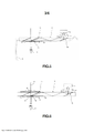
[0013] A Figura 1 é uma vista lateral de um exemplo de LOE da técnica anterior;[0013] Figure 1 is a side view of an example of prior art LOE;
[0014] A Figura 2 é um diagrama esquemático ilustrando um dispositivo óptico da técnica anterior para a colimação da entrada das ondas de luz a partir de uma fonte de luz de exibição;[0014] Figure 2 is a schematic diagram illustrating a prior art optical device for collimating incoming light waves from a display light source;
[0015] A Figura 3 é um diagrama esquemático ilustrando um sistema para a colimação e acoplamento da entrada de ondas de luz a partir de uma fonte de luz da exibição dentro de um n LOE, de acordo com a presente invenção;[0015] Figure 3 is a schematic diagram illustrating a system for collimating and coupling incoming light waves from a display light source within an n LOE, in accordance with the present invention;
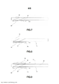
[0016] A Figura 4 é um diagrama esquemático ilustrando outra concretização para a colimação e acoplamento da entrada de ondas de luz a partir de uma fonte de luz da exibição dentro de um substrato, onde o módulo de colimação está anexado ao substrato, de acordo com a presente invenção;[0016] Figure 4 is a schematic diagram illustrating another embodiment for collimating and coupling incoming light waves from a display light source within a substrate, where the collimation module is attached to the substrate, in accordance with with the present invention;
[0017] A Figura 5 ilustra um exemplo de concretização onde uma lente negativa está anexada a uma superfície externa do elemento óptico de guia de luz, de acordo com a presente invenção;[0017] Figure 5 illustrates an example embodiment where a negative lens is attached to an external surface of the light guide optical element, according to the present invention;
[0018] A Figura 6 ilustra um exemplo de concretização onde as lentes positiva e negativa estão anexadas às superfícies externas do elemento óptico de guia de luz, de acordo com a presente invenção;[0018] Figure 6 illustrates an example of embodiment where the positive and negative lenses are attached to the external surfaces of the light guide optical element, according to the present invention;
[0019] A Figura 7 ilustra um exemplo de concretização onde uma lente negativa é cimentada a uma superfície externa do elemento óptico de guia luz utilizando adesivo de baixo índice refrativo, de acordo com a presente invenção;[0019] Figure 7 illustrates an example of an embodiment where a negative lens is cemented to an external surface of the light guide optical element using low refractive index adhesive, according to the present invention;
[0020] A Figura 8 ilustra um exemplo de concretização onde um substrato fabricado de um material de baixo índice refrativo está opticamente anexado a uma superfície externa do elemento óptico de guia luz, de acordo com a presente invenção;[0020] Figure 8 illustrates an example embodiment where a substrate made of a low refractive index material is optically attached to an outer surface of the light guide optical element, in accordance with the present invention;
[0021] A Figura 9 ilustra um exemplo de concretização onde as lentes negativas e positivas são cimentadas às superfícies externas do elemento óptico de guia luz utilizando duas camadas transparentes, de acordo com a presente invenção;[0021] Figure 9 illustrates an example of embodiment where the negative and positive lenses are cemented to the external surfaces of the light guide optical element using two transparent layers, according to the present invention;
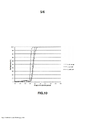
[0022] A Figura 10 é um gráfico ilustrando a curva de refletância para (a) um LOE não-cimentado; (b) um LOE cimentado a um substrato de material de baixo índice de e revestido com um revestimento antirreflexo e (c) um LOE cimentado ao substrato de material de baixo índice e revestido com um revestimento refletivo sensível angular, de acordo com a presente invenção;[0022] Figure 10 is a graph illustrating the reflectance curve for (a) an uncemented LOE; (b) an LOE cemented to a substrate of low-index material and coated with an anti-reflective coating; and (c) an LOE cemented to a substrate of low-index material and coated with an angle-sensitive reflective coating, in accordance with the present invention ;
[0023] A Figura 11 ilustra um exemplo de concretização da presente invenção, onde os elementos de acoplamento bem como de desacoplamento são elementos ópticos difrativos; e[0023] Figure 11 illustrates an example of embodiment of the present invention, where the coupling and decoupling elements are diffractive optical elements; and
[0024] A Figura 12 ilustra um exemplo de concretização da presente invenção, onde o módulo óptico é embutido em um sistema de exibição portátil.[0024] Figure 12 illustrates an example of embodiment of the present invention, where the optical module is embedded in a portable display system.
[0025] A Figura 1 ilustra uma vista em corte de um substrato 20 da técnica anterior e componentes associados (daqui em diante também referido como um “LOE”), utilizável na presente invenção. Um meio óptico, por exemplo, uma superfície refletora 16, é iluminada por um mostrador colimado de ondas de luz 18 a partir de uma exibição de uma fonte de luz (não mostrada). A superfície refletora 16 reflete as ondas de luz incidente a partir da fonte, de tal modo que as ondas de luz são capturadas dentro de um substrato plano 20 do LOE, por reflexão interna total. Após várias reflexões fora das superfícies superior e inferior principais 26, 28 do substrato 20, as ondas de luz capturadas alcançam um arranjo de superfícies refletoras seletivas 22, que acoplam as ondas de luz fora do substrato dentro de um olho 24, tendo uma pupila 25, de um observador. Aqui, a superfície de entrada do LOE será considerada como a superfície através da qual as ondas de luz de entrada entram no LOE e a superfície de saída do LOE será considerada como a superfície através da qual as ondas de luz capturadas saem do LOE. No caso do LOE ilustrado na Figura 1, ambas as superfícies de entrada e de saída estão sobre a superfície inferior 26. Outras configurações, no entanto, são previstas nas quais as ondas de luz de imagem e de entrada poderiam estar localizadas em lados opostos do substrato 20, ou quando as ondas de luz estão acopladas dentro do LOE através de uma borda inclinada do substrato.[0025] Figure 1 illustrates a sectional view of a
[0026] Conforme ilustrado na Figura 2, as ondas de luz de entrada s-polarizadas 2 a partir da fonte de luz da exibição 4 são acopladas dentro de um módulo de colimação 6, o qual é geralmente composto de um material transmissor de ondas de luz, através de sua superfície inferior 30. Seguindo fora da reflexão de um divisor de feixe de polarização 31, as ondas de luz são acopladas fora do substrato através da superfície 32 do módulo de colimação 6. As ondas de luz em seguida passam através de uma placa de retardamento de quarto de comprimento de onda 34, sendo refletidas por um elemento óptico de reflexão 36, por exemplo, um espelho plano, retornando a passar novamente através da placa de retardamento 34, e reentrando no módulo de colimação 6 através da superfície 32. As ondas de luz p-polarizadas agora passam através do divisor de feixe de polarização 31 e estão acopladas fora do guia de luz através da superfície 38 do módulo de colimação 6. As ondas de luz, em seguida, passam através de uma segunda placa de retardamento de quarto de comprimento de onda 40, sendo colimada por um componente 42, por exemplo, uma lente, na sua superfície refletora 44, retornando a passar novamente através da placa de retardamento 20, e reentrando no módulo de colimação 6 através da superfície 38. As ondas de luz s-polarizada são refletidas fora do divisor de feixe de polarização 31 e saem do módulo de colimação através da superfície superior 46. As superfícies refletoras 36 e 44 podem ser materializadas por qualquer um revestimento metálico ou um dielétrico.[0026] As illustrated in Figure 2, the incoming s-polarized light waves 2 from the display light source 4 are coupled within a
[0027] A Figura 3 ilustra como um módulo de colimação 6, constituído pelos componentes detalhados em relação à Figura 2, pode ser combinado com um LOE, para formar um sistema óptico. A saída das ondas de luz 48 a partir do módulo de colimação 6 entra no substrato 20 através da sua superfície inferior 26. As ondas de luz que entram (em comparação ao substrato 20) são refletidas a partir do elemento óptico 16 e capturadas no substrato, conforme ilustrado na Figura 2. Agora, o módulo de colimação 6, compreendendo a fonte de luz de exibição 4, os prismas de dobragem 52 e 54, o divisor de feixe de polarização 31, as placas de retardamento 34 e 40 e os elementos ópticos refletores 36 e 42, podem ser integrados dentro de um único módulo mecânico, os quais podem ser montados de forma independente do substrato, mesmo com tolerâncias mecânicas não precisas. Adicionalmente, as placas de retardamento 34 e 40 e os elementos ópticos refletores 36 e 42 podem ser cimentados juntos, respectivamente, para formar elementos individuais.[0027] Figure 3 illustrates how a
[0028] Seria vantajoso fixar todos os vários componentes do módulo de colimação 6 ao substrato 20 para formar um único elemento compacto com um módulo mecânico muito simplificado. A Figura 4 ilustra tal módulo, onde a superfície superior 46 do módulo de colimação 6 é fixada, no plano de interface 58, na superfície inferior 26 do LOE. O principal problema desta configuração é que o procedimento de fixação elimina o afastamento 50 previamente existente (ilustrado na Figura 3) entre o LOE e o módulo de colimação 6. Este afastamento é essencial para capturar a entrada das ondas de luz 48 dentro do LOE 20. Conforme ilustrado na Figura 4, as ondas de luz capturadas 48 devem ser refletidas nos pontos 62 e 64 no plano de interface 58. Deste modo, um arranjo óptico de reflexão deve ser aplicado neste plano, tanto na superfície principal 26 do LOE ou na superfície superior 46 do módulo de colimação 6. Um simples revestimento refletor não pode, no entanto, ser facilmente aplicado, uma vez que estas superfícies também devem ser transparentes para as ondas de luz que entram e saem do LOE nos pontos demonstrativos 66. As ondas de luz devem passar através do plano 64 em ângulos de incidência pequenos, e refletir em ângulos de incidência principais. Normalmente, os ângulos de incidência de passagem estão entre 0° e 15° e os ângulos de incidência refletores estão entre 38° e 80°.[0028] It would be advantageous to attach all the various components of the
[0029] Em todas as concretizações acima descritas da presente invenção, a imagem que é acoplada dentro do LOE é colimada para o infinito. Existem aplicações, no entanto, onde a imagem transmitida deve ser focada a uma distância mais próxima, por exemplo, para pessoas que sofrem de miopia e não podem ver corretamente imagens localizadas em longas distâncias.[0029] In all of the above-described embodiments of the present invention, the image that is coupled within the LOE is collimated to infinity. There are applications, however, where the transmitted image must be focused at a closer distance, for example for people who suffer from myopia and cannot correctly see images located at long distances.
[0030] A Figura 5 ilustra um método para implementação de uma lente, baseado com a presente invenção. Uma imagem 80 a partir do infinito é acoplada em um substrato 20 por uma superfície refletora 16 e depois refletida por um conjunto de superfícies parcialmente refletoras 22 dentro do olho 24 do observador. A lente oftálmica 82 foca as imagens a uma distância conveniente e, opcionalmente, corrige outras anomalias do olho do observador, incluindo astigmatismo. A lente de plano côncavo 82 pode ser anexada à superfície do substrato na sua superfície plana 84. Como explicado acima em relação à Figura 4, um pequeno afastamento deve ser preservado entre a lente 82 e o substrato 20, para garantir a captura dos feixes da imagem dentro do substrato através da reflexão interna total.[0030] Figure 5 illustrates a method for implementing a lens, based on the present invention. An
[0031] Adicionalmente, na maioria das aplicações relacionadas com a presente invenção, supõe-se que a cena externa está localizada no infinito. No entanto, existem aplicações, tais como, para finalidades profissionais ou médicas, onde a cena externa está localizada a uma distância mais próxima.[0031] Additionally, in most applications related to the present invention, the external scene is assumed to be located at infinity. However, there are applications, such as for professional or medical purposes, where the outdoor scene is located at a closer distance.
[0032] A Figura 6 ilustra um método para a implementação de uma configuração de lente dupla, com base na presente invenção. Uma imagem 80 a partir do infinito é acoplada dentro de um substrato 20 por uma superfície refletora 16 e, em seguida, refletida por um arranjo de superfícies parcialmente refletoras 22 dentro do olho 24 do observador. Outra imagem 86 da cena, a partir de uma distância mais próxima, é colimada ao infinito por uma lente 88 e, em seguida, passada através do substrato 20 dentro do olho. A lente 82 foca as imagens 80 e 86 a uma distância conveniente, geralmente a distância original da cena externa 86, e corrige outras anomalias do olho do observador, se necessário.[0032] Figure 6 illustrates a method for implementing a dual lens configuration, based on the present invention. An
[0033] As lentes 82 e 88 ilustradas nas Figuras 5 e 6 são lentes plano-côncavas e plano-convexas simples, respectivamente. No entanto, para manter a forma plana do LOE é possível ao contrário de utilizar lentes de Fresnel, as quais podem ser feitas de placas finas de plástico moldado com pequenos degraus. Além disso, uma forma alternativa para materializar as lentes 82 ou 88, ao contrário de utilizar lentes fixas conforme descrito acima, é a utilização de lentes dinâmicas controladas eletronicamente. Existem aplicações onde é requerido que o usuário seja capaz de não apenas ver uma imagem não colimada, mas também controlar dinamicamente o foco da imagem. Demonstrou-se que um modulador de luz espacial (SLM) de alta resolução pode ser utilizado para formar um elemento dinâmico. Atualmente, as fontes mais populares para essa finalidade são dispositivos LCD, mas outros dispositivos SLM dinâmicos podem ser também usados. Lentes dinâmicas de alta resolução tendo várias centenas de linhas/mm são conhecidas. Este tipo de lentes controladas eletro-opticamente pode ser utilizado como os elementos dinâmicos desejados na presente invenção, ao contrário das lentes fixas acima descritas em conjunto com as Figuras 5 e 6. Consequentemente, em tempo real, a operação pode determinar e definir os planos focais exatos de ambas a imagem virtual projetada pelo LOE e a imagem real da vista externa. Naturalmente, as lentes que estão ilustradas nas Figuras 5 e 6 podem facilmente serem montadas dentro de uma armação de óculos 83, conforme mostrado na Figura 5.[0033]
[0034] Conforme ilustrado acima na Figura 6, seria vantajoso fixar todas as lentes 82 e 88 ao LOE 20, para formar um elemento compacto simples com um módulo mecânico muito simplificado. O principal problema, conforme anteriormente descrito, é que o processo de fixação elimina o afastamento pré-existente entre o LOE 20 e as lentes 82 e 88, no qual é essencial para a captura das ondas de luz de entrada 80 dentro do LOE 20. Conforme ilustrado adicionalmente na Figura 6, as ondas de luz 80 retidas devem ser refletidas no ponto 90 do plano de interface 84 e transmitidas através do mesmo plano no ponto 92. Deste modo, um arranjo óptico de reflexão semelhante, ao descrito acima em relação à Figura 4, deve ser aplicado neste plano.[0034] As illustrated above in Figure 6, it would be advantageous to attach all
[0035] Uma abordagem possível para conseguir a disposição óptica de refracção necessária consiste em anexar opticamente uma camada transparente, tendo um índice refrativo que é substancialmente menor do que a do LOE, nas superfícies principais do LOE. Um método para materializar esta abordagem é cimentar o LOE ao elemento óptico necessário utilizando um adesivo de baixo índice refrativo. Existem adesivos ópticos disponíveis no mercado tendo um índice refrativo de -1,3.[0035] One possible approach to achieving the required refractive optical array is to optically attach a transparent layer, having a refractive index that is substantially lower than that of the LOE, on the main surfaces of the LOE. One method to materialize this approach is to cement the LOE to the required optical element using a low refractive index adhesive. There are optical adhesives available on the market having a refractive index of -1.3.
[0036] Conforme ilustrado na Figura 7, o índice refrativo baixo 100 é utilizado para cimentar a lente corretora 82 ao LOE. Os raios de luz que estão presos dentro do LOE agora estão totalmente refletidos a partir da superfície da interface 101 entre o adesivo 100 e o LOE. Este procedimento de cimentação não pode simplesmente substituir o afastamento necessário. Por exemplo, em um LOE que é fabricado de BK7, tendo um índice refrativo de 1,52, o ângulo crítico é 41,8°. Substituindo o afastamento com um adesivo de índice baixo írá aumentar o ângulo crítico para 58,8°. Com tal ângulo crítico alto, apenas uma FOV muito limitada pode ser capturada dentro do LOE através da reflexão interna total. No entanto, através da utilização de materiais de alto índice refrativo para a fabricação do LOE, o FOV alcançável pode ser aumentado. Utilizando um material óptico tendo um índice refrativo de 1,8 para a fabricação do LOE, por exemplo, reduzirá o ângulo crítico para 46,2°, o qual pode agora permitir um FOV mais razoável.[0036] As illustrated in Figure 7, the low
[0037] Uma concretização alternativa para aumentar o FOV é inserir uma fina camada intermediária de um material dielétrico sólido tendo um índice refrativo baixo entre o LOE e o elemento óptico anexado. Foi desenvolvida uma família de materiais de Aerogel tendo um índice refrativo muito baixo (na faixa de 1,1-1,2), bem como propriedades mecânicas estabilizadas. Outra alternativa possível para esta finalidade é um material dielétrico sólido poroso fabricado por deposição de ângulo oblíquo.[0037] An alternative embodiment to increase the FOV is to insert a thin intermediate layer of a solid dielectric material having a low refractive index between the LOE and the attached optical element. A family of Airgel materials has been developed having a very low refractive index (in the range of 1.1-1.2) as well as stabilized mechanical properties. Another possible alternative for this purpose is a porous solid dielectric material manufactured by oblique angle deposition.
[0038] A Figura 8 ilustra uma placa fina 104 de material de baixo índice (LIM) que é inserida entre o LOE e a lente corretora 82. Esta placa 104 de LIM pode tanto ser depositada diretamente sobre a superfície externa 26 do LOE ou cimentada a esta superfície utilizando uma camada adesiva fina 106. Para evitar reflexões múltiplas a partir de superfícies diferentes é preferível, neste caso, utilizar um adesivo tendo um índice refrativo semelhante ao do LOE. As reflexões internas dos raios retidos dentro do LOE serão a partir da superfície superior 107 da placa 104. Consequentemente, para evitar imagens múltiplas, esta superfície deve ser paralela à superfície externa 26 do LOE. Como um resultado, e também para evitar as tiras pretas na imagem, a espessura da camada adesiva 106 deve ser minimizada e, em qualquer caso, não mais do que algumas micra. Adicionalmente, a qualidade óptica e o nivelamento da superfície 107 deve ser muito elevada. Anexando uma placa de LIM à superfície principal do substrato para conseguir a disposição óptica sensível angular requerida, pode ser aplicada não apenas a uma das duas superfícies externas do LOE, mas bem como para a outra superfície.[0038] Figure 8 illustrates a
[0039] A Figura 9 ilustra uma segunda placa fina 108 de LIM, que é inserida entre o LOE 20 e a lente positiva 88, sendo que a superfície inferior 110 da placa está opticamente anexada à superfície superior 28 do LOE.[0039] Figure 9 illustrates a second
[0040] Outro procedimento que pode melhorar o desempenho de ambas as concretizações descritas acima, é adicionar um revestimento refletivo sensível angular (ASR), que aprisiona todo o FOV dentro do substrato, mesmo para ângulos menores do que o ângulo crítico da interface da superfície refletiva. Mesmo para aplicações não transparentes, onde uma das superfícies do substrato pode ser opaca e, consequentemente, pode ser revestida com uma superfície refletiva convencional, a superfície externa, a qual está próxima dos olhos do espectador, deve ser transparente, pelo menos para os ângulos do FOV externo requerido. Portanto, o revestimento refletivo necessário deve ter refletância muito elevada para a região de ângulos menores do que o ângulo crítico, e muito elevada refletância para todo o FOV da imagem.[0040] Another procedure that can improve the performance of both embodiments described above, is to add an angle sensitive reflective coating (ASR), which traps the entire FOV within the substrate, even for angles smaller than the critical angle of the surface interface. reflective. Even for non-transparent applications, where one of the substrate surfaces may be opaque and consequently may be coated with a conventional reflective surface, the outer surface, which is close to the viewer's eyes, must be transparent, at least for the angles. of the required external FOV. Therefore, the required reflective coating must have very high reflectance for the region of angles smaller than the critical angle, and very high reflectance for the entire FOV of the image.
[0041] A Figura 10 ilustra as curvas de refletância para um exemplo de concretização onde o LOE é fabricado de um material óptico tendo um índice refrativo de 1,6 e o comprimento de onda À=550 nm. Três gráficos diferentes são mostrados: a) A linha sólida representa a curva de refletância de um LOE não cimentado, ou seja, um LOE onde o material externo é ar e as superfícies externas do mesmo estão revestidas com um revestimento antirreflexo comum (AR). Conforme ilustrado, o ângulo crítico é de 38,7° e abaixo desse valor a refletância cai rapidamente. b) A linha pontilhada mostra a curva de refletância de um LOE que está cimentado a um substrato de LIM tendo um índice refrativo de 1,1 e a superfície de interface é revestida com um revestimento antirreflexo comum AR. Aqui, o ângulo crítico é aumentado para 43,4°. O FOV potencial que pode ser acoplado dentro do LOE é diminuído, mas ainda é razoável e semelhante ao LOE não cimentado fabricado de BK7 onde o ângulo crítico é 41,8°. c) A linha tracejada representa a curva de refletância de um LOE, o qual é cimentado a um substrato de LIM, tendo um índice refrativo de 1,1. Aqui, a superfície de interface, no entanto, é revestida com um revestimento ASR especial. O arranjo óptico da reflexão dos raios retidos dentro do LOE a partir da superfície de interface, em ângulos de incidência menores que 43,4°, não está afastado de uma reflexão interna total, mas, ao contrário, de uma reflexão a partir do revestimento ASR. A refletância dos raios que incidem sobre a superfície da interface em ângulos de incidência principais que 34,7°C é superior que 99%, e os raios são praticamente, de forma total, refletidos a partir da superfície da interface. Como um resultado, o FOV potencial que pode ser retido dentro deste LOE é consideravelmente mais elevado do que a de um LOE não cimentado, o qual é ilustrado no gráfico (a).[0041] Figure 10 illustrates the reflectance curves for an example embodiment where the LOE is manufactured from an optical material having a refractive index of 1.6 and wavelength Δ=550 nm. Three different graphs are shown: a) The solid line represents the reflectance curve of an uncemented LOE, that is, an LOE where the outer material is air and the outer surfaces of the same are coated with a common anti-reflective coating (AR). As illustrated, the critical angle is 38.7° and below this value the reflectance drops rapidly. b) The dotted line shows the reflectance curve of an LOE that is cemented to a LIM substrate having a refractive index of 1.1 and the interface surface is coated with a common AR anti-reflective coating. Here, the critical angle is increased to 43.4°. The potential FOV that can be coupled within the LOE is decreased but is still reasonable and similar to uncemented LOE fabricated from BK7 where the critical angle is 41.8°. c) The dashed line represents the reflectance curve of an LOE, which is cemented to a LIM substrate, having a refractive index of 1.1. Here, the interface surface, however, is coated with a special ASR coating. The optical arrangement of the reflection of rays retained within the LOE from the interface surface, at angles of incidence less than 43.4°, is not far from total internal reflection, but rather from reflection from the coating. RSA The reflectance of rays that strike the surface of the interface at principal angles of incidence that 34.7°C is greater than 99%, and the rays are practically entirely reflected from the surface of the interface. As a result, the potential FOV that can be retained within this LOE is considerably higher than that of an uncemented LOE, which is illustrated in graph (a).
[0042] Existem duas regiões significativas neste gráfico: entre 34° e 90°, onde a refletância é muito elevada, e entre 0° e 29° (equivalente a 0°-46° do lado de fora do substrato), onde a refletância é muito baixa. Assim, enquanto se pode assegurar que todo o espectro angular das ondas ópticas retidas, onde reflexões muito elevadas são desejadas, será localizado dentro da primeira região, enquanto todo o espectro angular do FOV externo onde, essencialmente, quaisquer reflexões são necessárias, será localizado dentro da segunda região, para um dado FOV, todo o FOV será retido dentro do substrato através das reflexões internas e de modo que o espectador possa ver a imagem inteira.[0042] There are two significant regions in this graph: between 34° and 90°, where the reflectance is very high, and between 0° and 29° (equivalent to 0°-46° outside the substrate), where the reflectance it is very low. Thus, while it can be assured that the entire angular spectrum of the retained optical waves, where very high reflections are desired, will be located within the first region, while the entire angular spectrum of the outer FOV where essentially any reflections are needed, will be located within from the second region, for a given FOV, the entire FOV will be retained within the substrate through internal reflections and so that the viewer can see the entire image.
[0043] Quando um substrato LIM é cimentado à superfície superior do LOE o revestimento ASR pode ser aplicado à superfície externa 107 (Figura 9) da placa de LIM, a qual está localizada adjacente ao LOE como explicado acima. Se a camada de LIM é, no entanto, depositada diretamente sobre o LOE, a única maneira de aplicar o revestimento ASR necessário é sobre a superfície externa 26 do LOE. Uma vez que o processo de fabricação do LOE geralmente envolve elementos ópticos de cimentação, e uma vez que o revestimento ASR necessário é aplicado à superfície do substrato apenas após o corpo do LOE estar completo, não é possível utilizar os procedimentos de revestimento a quente convencionais que podem danificar as áreas cimentadas. Novas tecnologias de película fina, tais como, procedimentos de revestimento assistida por íons, podem também ser usadas para o processamento à frio, eliminando a necessidade de aquecer as peças as quais permitem que as peças cimentadas, tais como LOES, sejam revestidas com segurança.[0043] When a LIM substrate is cemented to the upper surface of the LOE the ASR coating can be applied to the outer surface 107 (Figure 9) of the LIM plate, which is located adjacent to the LOE as explained above. If the LIM layer is, however, deposited directly over the LOE, the only way to apply the required ASR coating is over the
[0044] Em todas as concretizações ilustradas até agora o elemento para o acoplamento das ondas de luz fora do substrato é pelo menos uma superfície de reflexão parcialmente plana localizada no referido substrato, que é geralmente revestido com um revestimento dielétrico de reflexão parcial e não sendo paralelo às superfícies principais do referido substrato. No entanto, o arranjo óptico refletor particular, de acordo com a presente invenção, pode ser também explorado para outras tecnologias de acoplamento de saída.[0044] In all the embodiments illustrated so far the element for coupling the light waves outside the substrate is at least a partially planar reflecting surface located on said substrate, which is generally coated with a dielectric coating of partial reflection and not being parallel to the main surfaces of said substrate. However, the particular reflector optical arrangement according to the present invention can be exploited for other output coupling technologies as well.
[0045] A Figura 11 ilustra um substrato 20, onde o elemento de acoplamento de entrada 102, ou o elemento de acoplamento de saída 104 são elementos difrativos e um substrato fino LIM está opticamente cimentado à superfície superior 28 do substrato. Além disso, outros elementos de acoplamento de saída, tal como uma superfície de reflexão parcialmente curvada, e outros meios, podem ser utilizados.[0045] Figure 11 illustrates a
[0046] Os elementos das Figuras 5-9 são apenas alguns exemplos ilustrando a simples implementação da presente invenção dentro de uma armação de óculos. Uma vez que o elemento óptico de substrato guiado, constituindo o núcleo do sistema, é muito compacto e leve, podendo ser instalado em uma grande variedade de arranjos. Muitas outras concretizações são também possíveis, incluindo um visor, um mostrador dobrável, um monóculo, e muitos outros. Esta concretização é concebida para aplicações onde o mostrador deve estar próximo-ao-olho, montado na cabeça, vestido na cabeça ou carregado na cabeça. Existem, no entanto, aplicações onde o mostrador está localizado de forma diferente. Um exemplo de tal aplicação é um dispositivo portátil para aplicação móvel, tal como, por exemplo, um smartphone ou smartwatch. O principal problema destes dispositivos inteligentes é a contradição entre o tamanho e o volume pequeno necessários e a imagem de alta qualidade desejada.[0046] The elements of Figures 5-9 are just a few examples illustrating the simple implementation of the present invention within an eyeglass frame. Since the substrate-guided optical element, constituting the core of the system, is very compact and lightweight, it can be installed in a wide variety of arrangements. Many other embodiments are also possible, including a visor, a collapsible dial, a monocle, and many others. This embodiment is designed for applications where the dial must be close-to-the-eye, head-mounted, head-worn, or head-worn. There are, however, applications where the display is located differently. An example of such an application is a portable device for mobile application, such as, for example, a smartphone or smartwatch. The main problem with these smart devices is the contradiction between the small size and volume required and the desired high quality image.
[0047] A Figura 12 ilustra uma concretização alternativa, com base na presente invenção, que elimina o compromisso necessário entre o tamanho reduzido de dispositivos móveis e o desejo de ver o conteúdo digital em um mostrador de formato completo. Esta aplicação é um mostrador portátil (HHD) que resolve os requisitos previamente opostos, de alcançar pequenos dispositivos móveis, e o desejo de visualizar o conteúdo digital em um mostrador de formato completo, projetando imagens de alta qualidade diretamente no olho do usuário. Um módulo óptico incluindo a fonte de exibição 4, a óptica de dobragem e colimação 108 e o substrato 20 é integrado no corpo de um dispositivo inteligente 110, onde o substrato 20 substitui a janela de cobertura protetiva existente do telefone. Especificamente, o volume dos componentes de suporte, incluindo a fonte 4 e óptica 108, é suficientemente pequeno para encaixar dentro do tamanho aceitável para os dispositivos inteligentes modernos. A fim de visualizar o mostrador completo transmitido pelo dispositivo, a janela do dispositivo é posicionada na frente do olho do usuário 24, observando a imagem com alto FOV, uma grande caixa de movimento ocular e um confortável relevo de olho. Também é possível visualizar todo o FOV em um relevo de olho maior ao inclinar o dispositivo para exibir diferentes partes da imagem. Além disso, uma vez que o módulo óptico possa operar em configuração transparente, uma operação dupla do dispositivo é possível, ou seja, não é uma opção manter o mostrador convencional 112 intacto. Desta forma, o mostrador padrão pode ser visto através do substrato 20 quando a fonte de exibição 4 é desligada. Em um segundo modo virtual, designado pela maciça navegação na internet, ou operações de vídeo de alta qualidade, a visualização convencional 112 é desligada, enquanto a fonte de exibição 4 projeta a imagem FOV larga necessária no olho do observador por meio do substrato 20. Geralmente, na maioria dos dispositivos inteligentes portáteis, o usuário pode operar o dispositivo inteligente utilizando uma tela sensível ao toque que é incorporada na janela frontal do dispositivo. Conforme ilustrado na Figura 12, a tela sensível ao toque 114 pode ser anexada a um dispositivo inteligente pela sua cimentação direta sobre as superfícies externas de uma camada 120 de LIM que estão localizadas no substrato 20.[0047] Figure 12 illustrates an alternative embodiment, based on the present invention, that eliminates the necessary compromise between the small size of mobile devices and the desire to view digital content in a full-format display. This application is a portable display (HHD) that solves the previously opposing requirements of reaching small mobile devices and the desire to view digital content in a full-format display, projecting high quality images directly into the user's eye. An optical module including display source 4, folding and
Claims (18)
Applications Claiming Priority (3)
| Application Number | Priority Date | Filing Date | Title |
|---|---|---|---|
| IL236490 | 2014-12-25 | ||
| IL236490A IL236490B (en) | 2014-12-25 | 2014-12-25 | Substrate-guided optical device |
| PCT/IL2015/051222 WO2016103251A1 (en) | 2014-12-25 | 2015-12-16 | Substrate-guided optical device |
Publications (2)
| Publication Number | Publication Date |
|---|---|
| BR112017013680A2 BR112017013680A2 (en) | 2018-03-13 |
| BR112017013680B1 true BR112017013680B1 (en) | 2022-07-26 |
Family
ID=54347971
Family Applications (1)
| Application Number | Title | Priority Date | Filing Date |
|---|---|---|---|
| BR112017013680-5A BR112017013680B1 (en) | 2014-12-25 | 2015-12-16 | OPTICAL SYSTEM |
Country Status (11)
| Country | Link |
|---|---|
| US (3) | US20180067315A1 (en) |
| EP (2) | EP3715935A1 (en) |
| JP (3) | JP6779211B2 (en) |
| KR (2) | KR102292535B1 (en) |
| CN (2) | CN111240019B (en) |
| BR (1) | BR112017013680B1 (en) |
| CA (1) | CA2969822C (en) |
| IL (1) | IL236490B (en) |
| RU (1) | RU2721661C2 (en) |
| SG (2) | SG10202001056XA (en) |
| WO (1) | WO2016103251A1 (en) |
Families Citing this family (74)
| Publication number | Priority date | Publication date | Assignee | Title |
|---|---|---|---|---|
| IL166799A (en) | 2005-02-10 | 2014-09-30 | Lumus Ltd | Substrate-guided optical device utilizing beam splitters |
| US10073264B2 (en) | 2007-08-03 | 2018-09-11 | Lumus Ltd. | Substrate-guide optical device |
| US10261321B2 (en) | 2005-11-08 | 2019-04-16 | Lumus Ltd. | Polarizing optical system |
| IL219907A (en) | 2012-05-21 | 2017-08-31 | Lumus Ltd | Head-mounted display eyeball tracker integrated system |
| IL232197B (en) | 2014-04-23 | 2018-04-30 | Lumus Ltd | Compact head-mounted display system |
| IL235642B (en) | 2014-11-11 | 2021-08-31 | Lumus Ltd | Compact head-mounted display system protected by a hyperfine structure |
| IL237337B (en) | 2015-02-19 | 2020-03-31 | Amitai Yaakov | Compact head-mounted display system having uniform image |
| DE102016105060B3 (en) | 2016-03-18 | 2017-07-06 | Carl Zeiss Smart Optics Gmbh | Spectacle lens for imaging optics, imaging optics and data glasses |
| KR20230066124A (en) | 2016-10-09 | 2023-05-12 | 루머스 리미티드 | Aperture multiplier using a rectangular waveguide |
| RU2763850C2 (en) * | 2016-11-08 | 2022-01-11 | Люмус Лтд | Lightguide device with edge providing optical cutoff and corresponding manufacturing methods |
| CN110431467A (en) * | 2017-01-28 | 2019-11-08 | 鲁姆斯有限公司 | Augmented reality imaging system |
| KR102338472B1 (en) | 2017-02-22 | 2021-12-14 | 루머스 리미티드 | light guide optical assembly |
| KR20180106624A (en) * | 2017-03-21 | 2018-10-01 | 주식회사 파노비젼 | Optic system of see-through head mounted display having expanding manners for horizontal and vertical exit pupils |
| CN117572644A (en) | 2017-03-22 | 2024-02-20 | 鲁姆斯有限公司 | Method for producing a light-guiding optical element and optical system |
| IL251645B (en) | 2017-04-06 | 2018-08-30 | Lumus Ltd | Light-guide optical element and method of its manufacture |
| JP2020521170A (en) * | 2017-05-19 | 2020-07-16 | シーリアル テクノロジーズ ソシエテ アノニムSeereal Technologies S.A. | Display device with light guide |
| CN110869839B (en) | 2017-07-19 | 2022-07-08 | 鲁姆斯有限公司 | Liquid crystal on silicon illuminator with light guide optical element |
| KR102561362B1 (en) | 2017-09-29 | 2023-07-28 | 루머스 리미티드 | augmented reality display |
| CN111465888B (en) * | 2017-10-16 | 2022-11-22 | 奥里姆光学有限公司 | High-efficient compact head-mounted display system |
| CN111133362B (en) | 2017-10-22 | 2021-12-28 | 鲁姆斯有限公司 | Head-mounted augmented reality device employing optical bench |
| CA3082067C (en) | 2017-11-21 | 2023-08-01 | Lumus Ltd. | Optical aperture expansion arrangement for near-eye displays |
| WO2019106636A1 (en) | 2017-12-03 | 2019-06-06 | Lumus Ltd. | Optical device testing method and apparatus |
| KR20200096274A (en) | 2017-12-03 | 2020-08-11 | 루머스 리미티드 | Optical device alignment method |
| CN107966819A (en) * | 2017-12-27 | 2018-04-27 | 北京灵犀微光科技有限公司 | Waveguide display device |
| US10506220B2 (en) | 2018-01-02 | 2019-12-10 | Lumus Ltd. | Augmented reality displays with active alignment and corresponding methods |
| MX2020002402A (en) | 2018-01-02 | 2020-07-22 | Lumus Ltd | Augmented reality displays with active alignment and corresponding methods. |
| US10551544B2 (en) * | 2018-01-21 | 2020-02-04 | Lumus Ltd. | Light-guide optical element with multiple-axis internal aperture expansion |
| US11221294B2 (en) | 2018-04-08 | 2022-01-11 | Lumus Ltd. | Optical sample characterization |
| US10830938B2 (en) | 2018-05-14 | 2020-11-10 | Lumus Ltd. | Projector configuration with subdivided optical aperture for near-eye displays, and corresponding optical systems |
| EP3794397A4 (en) | 2018-05-17 | 2021-07-07 | Lumus Ltd. | Near-eye display having overlapping projector assemblies |
| IL259518B2 (en) | 2018-05-22 | 2023-04-01 | Lumus Ltd | Optical system and method for improvement of light field uniformity |
| TWI813691B (en) | 2018-05-23 | 2023-09-01 | 以色列商魯姆斯有限公司 | Optical system including light-guide optical element with partially-reflective internal surfaces |
| WO2019244093A1 (en) | 2018-06-21 | 2019-12-26 | Lumus Ltd. | Measurement technique for refractive index inhomogeneity between plates of a lightguide optical element (loe) |
| US11415812B2 (en) | 2018-06-26 | 2022-08-16 | Lumus Ltd. | Compact collimating optical device and system |
| US11409103B2 (en) | 2018-07-16 | 2022-08-09 | Lumus Ltd. | Light-guide optical element employing polarized internal reflectors |
| JP7183611B2 (en) * | 2018-07-30 | 2022-12-06 | セイコーエプソン株式会社 | virtual image display |
| JP7407458B2 (en) * | 2018-09-09 | 2024-01-04 | ルムス エルティーディー. | Optical system including light-guiding optical element with two-dimensional extension |
| US11803056B2 (en) * | 2018-09-14 | 2023-10-31 | Apple Inc. | Waveguided display systems |
| CN111077670B (en) * | 2018-10-18 | 2022-02-18 | 中强光电股份有限公司 | Light transmission module and head-mounted display device |
| TW202026685A (en) * | 2018-11-08 | 2020-07-16 | 以色列商魯姆斯有限公司 | Light-guide display with reflector |
| EP3867696B1 (en) | 2018-11-08 | 2022-08-03 | Lumus Ltd. | Optical devices and systems with dichroic beamsplitter color combiner |
| JP3226277U (en) | 2018-11-11 | 2020-05-14 | ルムス エルティーディー. | Near eye display with intermediate window |
| CN109445109A (en) * | 2018-12-26 | 2019-03-08 | 深圳珑璟光电技术有限公司 | A kind of light-transmitting plate |
| CN109683317A (en) * | 2018-12-28 | 2019-04-26 | 北京灵犀微光科技有限公司 | Augmented reality eyepiece device and augmented reality display device |
| CN110146980A (en) * | 2018-12-29 | 2019-08-20 | 深圳珑璟光电技术有限公司 | A kind of substrate-guided optical device |
| KR20210114925A (en) * | 2019-01-20 | 2021-09-24 | 루머스 리미티드 | Optical device test method and apparatus |
| WO2020152688A1 (en) | 2019-01-24 | 2020-07-30 | Lumus Ltd. | Optical systems including loe with three stage expansion |
| IL264551A (en) | 2019-01-29 | 2020-07-30 | Amitai Yaakov | Highly efficient compact head-mounted display system having small input aperture |
| US10942320B2 (en) * | 2019-02-11 | 2021-03-09 | Facebook Technologies, Llc | Dispersion compensation for light coupling through slanted facet of optical waveguide |
| US11849262B2 (en) | 2019-03-12 | 2023-12-19 | Lumus Ltd. | Image projector |
| US11048087B2 (en) | 2019-06-10 | 2021-06-29 | Facebook Technologies, Llc | Optical assemblies having polarization volume gratings for projecting augmented reality content |
| US11181815B1 (en) | 2019-06-11 | 2021-11-23 | Facebook Technologies, Llc | Optical devices including reflective spatial light modulators for projecting augmented reality content |
| BR112021022229A2 (en) | 2019-06-27 | 2022-02-22 | Lumus Ltd | Device |
| JP2021071604A (en) * | 2019-10-31 | 2021-05-06 | セイコーエプソン株式会社 | Light guide device, display device, and method for manufacturing light guide device |
| KR102622406B1 (en) | 2019-11-25 | 2024-01-05 | 루머스 리미티드 | How to polish the surface of a waveguide |
| IL270991B (en) * | 2019-11-27 | 2020-07-30 | Lumus Ltd | Lightguide optical element for polarization scrambling |
| CA3162579C (en) | 2019-12-05 | 2024-01-30 | Lumus Ltd | Light-guide optical element employing complementary coated partial reflectors, and light-guide optical element having reduced light scattering |
| EP4042232A4 (en) | 2019-12-08 | 2022-12-28 | Lumus Ltd. | Optical systems with compact image projector |
| US11029564B1 (en) * | 2019-12-19 | 2021-06-08 | Lumileds Llc | Polarizing edge coupled light in backlight |
| TWI718054B (en) * | 2020-04-23 | 2021-02-01 | 宏碁股份有限公司 | Optical device combining spectacle function with augmented reality function and augmented reality device |
| US11330091B2 (en) | 2020-07-02 | 2022-05-10 | Dylan Appel-Oudenaar | Apparatus with handheld form factor and transparent display with virtual content rendering |
| US11526016B1 (en) * | 2020-07-02 | 2022-12-13 | Meta Platforms Technologies, Llc | Spatial light modulator displays with divergence correction lens |
| US11539929B1 (en) | 2020-07-02 | 2022-12-27 | Meta Platforms Technologies, Llc. | Spatial light modulator displays with diffractive optical elements |
| US11726365B1 (en) | 2020-07-10 | 2023-08-15 | Meta Platforms Technologies, Llc | Optical assembly for providing koehller illumination to a display |
| DE202021104723U1 (en) | 2020-09-11 | 2021-10-18 | Lumus Ltd. | Image projector coupled to an optical light guide element |
| DE102020006442B3 (en) * | 2020-10-13 | 2021-10-28 | Sioptica Gmbh | Optical element with variable transmission, method for producing such an optical element and use of such an optical element in a screen |
| US11747137B2 (en) | 2020-11-18 | 2023-09-05 | Lumus Ltd. | Optical-based validation of orientations of internal facets |
| KR102620208B1 (en) | 2021-02-25 | 2023-12-29 | 루머스 리미티드 | Optical aperture multiplier with rectangular waveguide |
| EP4237903A4 (en) | 2021-03-01 | 2024-04-24 | Lumus Ltd | Optical system with compact coupling from a projector into a waveguide |
| US11789264B2 (en) | 2021-07-04 | 2023-10-17 | Lumus Ltd. | Display with stacked light-guide elements providing different parts of field of view |
| CN116413911A (en) * | 2021-12-31 | 2023-07-11 | 北京耐德佳显示技术有限公司 | Ultra-thin lens, virtual image imaging device using same and near-eye display |
| CN115453678B (en) * | 2022-01-30 | 2023-08-29 | 珠海莫界科技有限公司 | Optical combiner and display device |
| DE102022117022A1 (en) | 2022-07-07 | 2024-01-18 | Carl Zeiss Ag | Method for producing an optical arrangement comprising an optical waveguide and an optical component |
| WO2024043515A1 (en) * | 2022-08-25 | 2024-02-29 | 삼성전자 주식회사 | Display device for providing immersive image |
Family Cites Families (53)
| Publication number | Priority date | Publication date | Assignee | Title |
|---|---|---|---|---|
| AT390677B (en) * | 1986-10-10 | 1990-06-11 | Avl Verbrennungskraft Messtech | SENSOR ELEMENT FOR DETERMINING SUBSTANCE CONCENTRATIONS |
| EP0867747A3 (en) * | 1997-03-25 | 1999-03-03 | Sony Corporation | Reflective display device |
| IL121067A0 (en) * | 1997-06-12 | 1997-11-20 | Yeda Res & Dev | Compact planar optical correlator |
| JP2001242412A (en) * | 2000-02-28 | 2001-09-07 | Sony Corp | Virtual image viewing optical system |
| JP2001264683A (en) * | 2000-03-17 | 2001-09-26 | Minolta Co Ltd | Information display optical system, optical element or optical system and information display device |
| ATE473464T1 (en) * | 2000-06-05 | 2010-07-15 | Lumus Ltd | OPTICAL BEAM EXPANDER WITH SUBSTRATE LIGHT WAVE GUIDE |
| US20040176488A1 (en) * | 2000-06-06 | 2004-09-09 | Shyama Mukherjee | Low dielectric materials and methods of producing same |
| KR20020083737A (en) * | 2001-04-30 | 2002-11-04 | 삼성전자 주식회사 | Wearable display system |
| JP2003149643A (en) * | 2001-11-16 | 2003-05-21 | Goyo Paper Working Co Ltd | Front light for liquid crystal display |
| IL148804A (en) | 2002-03-21 | 2007-02-11 | Yaacov Amitai | Optical device |
| JP2004178708A (en) * | 2002-11-27 | 2004-06-24 | Tdk Corp | Magnetic recording medium and magnetic recorder |
| IL157837A (en) * | 2003-09-10 | 2012-12-31 | Yaakov Amitai | Substrate-guided optical device particularly for three-dimensional displays |
| IL157836A (en) | 2003-09-10 | 2009-08-03 | Yaakov Amitai | Optical devices particularly for remote viewing applications |
| WO2005088384A1 (en) * | 2004-03-12 | 2005-09-22 | Nikon Corporation | Image display optical system and image display apparatus |
| JP4373286B2 (en) * | 2004-05-06 | 2009-11-25 | オリンパス株式会社 | Head-mounted display device |
| JP4609160B2 (en) * | 2004-05-17 | 2011-01-12 | 株式会社ニコン | Optical element, combiner optical system, and information display device |
| EP1748305A4 (en) * | 2004-05-17 | 2009-01-14 | Nikon Corp | Optical element, combiner optical system, and image display unit |
| CN1957269A (en) * | 2004-05-17 | 2007-05-02 | 株式会社尼康 | Optical elements and combiner optical systems and image-display units |
| IL162572A (en) | 2004-06-17 | 2013-02-28 | Lumus Ltd | High brightness optical device |
| IL163361A (en) | 2004-08-05 | 2011-06-30 | Lumus Ltd | Optical device for light coupling into a guiding substrate |
| US7778508B2 (en) * | 2004-12-06 | 2010-08-17 | Nikon Corporation | Image display optical system, image display unit, illuminating optical system, and liquid crystal display unit |
| WO2006085310A1 (en) | 2005-02-10 | 2006-08-17 | Lumus Ltd. | Substrate-guided optical device particularly for vision enhanced optical systems |
| EP1849033B1 (en) | 2005-02-10 | 2019-06-19 | Lumus Ltd | Substrate-guided optical device utilizing thin transparent layer |
| EP1848966A1 (en) | 2005-02-17 | 2007-10-31 | Lumus Ltd | Personal navigation system |
| FR2883078B1 (en) * | 2005-03-10 | 2008-02-22 | Essilor Int | OPTICAL IMAGER FOR REALIZING AN OPTICAL DISPLAY |
| IL171820A (en) | 2005-11-08 | 2014-04-30 | Lumus Ltd | Polarizing optical device for light coupling |
| IL173715A0 (en) | 2006-02-14 | 2007-03-08 | Lumus Ltd | Substrate-guided imaging lens |
| IL177618A (en) | 2006-08-22 | 2015-02-26 | Lumus Ltd | Substrate- guided optical device |
| JP2008107521A (en) * | 2006-10-25 | 2008-05-08 | Seiko Epson Corp | Light source device, illuminating device and image display device |
| WO2008129539A2 (en) | 2007-04-22 | 2008-10-30 | Lumus Ltd. | A collimating optical device and system |
| IL183637A (en) | 2007-06-04 | 2013-06-27 | Zvi Lapidot | Distributed head-mounted display |
| JP2009021914A (en) * | 2007-07-13 | 2009-01-29 | Sony Corp | Imaging display system, imaging display device, and control method of imaging display device |
| JP4395802B2 (en) * | 2007-11-29 | 2010-01-13 | ソニー株式会社 | Image display device |
| JP5022312B2 (en) * | 2008-06-18 | 2012-09-12 | 株式会社ジャパンディスプレイイースト | Manufacturing method of liquid crystal display device |
| JP4246254B2 (en) * | 2008-07-15 | 2009-04-02 | オリンパス株式会社 | Prism optical element and image observation apparatus |
| JP4858512B2 (en) * | 2008-08-21 | 2012-01-18 | ソニー株式会社 | Head-mounted display |
| KR101114646B1 (en) * | 2008-12-08 | 2012-03-05 | 삼성전자주식회사 | Touch screen |
| EP2376971B1 (en) * | 2008-12-12 | 2019-02-20 | BAE Systems PLC | Improvements in or relating to waveguides |
| JP5545076B2 (en) * | 2009-07-22 | 2014-07-09 | ソニー株式会社 | Image display device and optical device |
| JP5499854B2 (en) * | 2010-04-08 | 2014-05-21 | ソニー株式会社 | Optical position adjustment method for head mounted display |
| KR101207852B1 (en) * | 2010-05-07 | 2012-12-04 | 한국광기술원 | Planar type high concentration photovoltaic power generator module and sun tracker using this module |
| JP5459150B2 (en) * | 2010-09-03 | 2014-04-02 | セイコーエプソン株式会社 | Light guide plate and virtual image display device including the same |
| JP5471986B2 (en) * | 2010-09-07 | 2014-04-16 | 株式会社島津製作所 | Optical component and display device using the same |
| JP5855117B2 (en) * | 2010-11-08 | 2016-02-09 | スリーエム イノベイティブ プロパティズ カンパニー | Lighting converter |
| JP5747538B2 (en) * | 2011-02-04 | 2015-07-15 | セイコーエプソン株式会社 | Virtual image display device |
| US8665178B1 (en) * | 2012-03-01 | 2014-03-04 | Google, Inc. | Partially-reflective waveguide stack and heads-up display using same |
| US8848289B2 (en) * | 2012-03-15 | 2014-09-30 | Google Inc. | Near-to-eye display with diffractive lens |
| IL219907A (en) | 2012-05-21 | 2017-08-31 | Lumus Ltd | Head-mounted display eyeball tracker integrated system |
| US20140168260A1 (en) * | 2012-12-13 | 2014-06-19 | Paul M. O'Brien | Waveguide spacers within an ned device |
| JP6264734B2 (en) * | 2013-03-13 | 2018-01-24 | セイコーエプソン株式会社 | Virtual image display device |
| US9946069B2 (en) * | 2013-03-28 | 2018-04-17 | Bae Systems Plc | Displays |
| US9477033B2 (en) * | 2013-04-23 | 2016-10-25 | Lumenco, Llc | Multi-layered waveguide for capturing solar energy |
| DE102013106392B4 (en) * | 2013-06-19 | 2017-06-08 | Fraunhofer-Gesellschaft zur Förderung der angewandten Forschung e.V. | Process for producing an antireflection coating |
-
2014
- 2014-12-25 IL IL236490A patent/IL236490B/en unknown
-
2015
- 2015-12-16 RU RU2017122204A patent/RU2721661C2/en active
- 2015-12-16 CN CN202010173104.8A patent/CN111240019B/en active Active
- 2015-12-16 EP EP20156833.4A patent/EP3715935A1/en active Pending
- 2015-12-16 CA CA2969822A patent/CA2969822C/en active Active
- 2015-12-16 JP JP2017534237A patent/JP6779211B2/en active Active
- 2015-12-16 KR KR1020177016925A patent/KR102292535B1/en active IP Right Grant
- 2015-12-16 US US15/537,269 patent/US20180067315A1/en not_active Abandoned
- 2015-12-16 SG SG10202001056XA patent/SG10202001056XA/en unknown
- 2015-12-16 EP EP15831162.1A patent/EP3237954A1/en not_active Ceased
- 2015-12-16 CN CN201580070553.7A patent/CN107111129B/en active Active
- 2015-12-16 SG SG11201704276TA patent/SG11201704276TA/en unknown
- 2015-12-16 KR KR1020207005021A patent/KR102578625B1/en active IP Right Grant
- 2015-12-16 WO PCT/IL2015/051222 patent/WO2016103251A1/en active Application Filing
- 2015-12-16 BR BR112017013680-5A patent/BR112017013680B1/en active IP Right Grant
-
2020
- 2020-02-12 US US16/788,375 patent/US20200183170A1/en not_active Abandoned
- 2020-02-26 JP JP2020030352A patent/JP6966104B2/en active Active
- 2020-04-27 US US16/858,757 patent/US20200326545A1/en not_active Abandoned
-
2021
- 2021-10-14 JP JP2021168461A patent/JP2022009123A/en active Pending
Also Published As
| Publication number | Publication date |
|---|---|
| BR112017013680A2 (en) | 2018-03-13 |
| JP6966104B2 (en) | 2021-11-10 |
| CN107111129A (en) | 2017-08-29 |
| US20200326545A1 (en) | 2020-10-15 |
| CA2969822A1 (en) | 2016-06-30 |
| SG11201704276TA (en) | 2017-07-28 |
| KR20170097661A (en) | 2017-08-28 |
| KR102292535B1 (en) | 2021-08-23 |
| US20200183170A1 (en) | 2020-06-11 |
| RU2721661C2 (en) | 2020-05-21 |
| CN107111129B (en) | 2021-04-09 |
| RU2017122204A (en) | 2018-12-24 |
| JP2018503865A (en) | 2018-02-08 |
| SG10202001056XA (en) | 2020-04-29 |
| CA2969822C (en) | 2023-07-04 |
| WO2016103251A1 (en) | 2016-06-30 |
| US20180067315A1 (en) | 2018-03-08 |
| KR102578625B1 (en) | 2023-09-13 |
| JP2022009123A (en) | 2022-01-14 |
| EP3237954A1 (en) | 2017-11-01 |
| IL236490B (en) | 2021-10-31 |
| EP3715935A1 (en) | 2020-09-30 |
| JP2020106855A (en) | 2020-07-09 |
| IL236490A0 (en) | 2015-04-30 |
| CN111240019A (en) | 2020-06-05 |
| RU2017122204A3 (en) | 2019-04-12 |
| CN111240019B (en) | 2022-06-24 |
| KR20200021001A (en) | 2020-02-26 |
| JP6779211B2 (en) | 2020-11-04 |
Similar Documents
| Publication | Publication Date | Title |
|---|---|---|
| BR112017013680B1 (en) | OPTICAL SYSTEM | |
| US10782532B2 (en) | Compact head-mounted display system protected by a hyperfine structure | |
| TWI712821B (en) | Optical system, augmented reality system, head up display system, electronic device and optical module | |
| US9104036B2 (en) | Collimating optical device and system | |
| US11892640B1 (en) | Waveguide combiner with stacked plates |
Legal Events
| Date | Code | Title | Description |
|---|---|---|---|
| B06U | Preliminary requirement: requests with searches performed by other patent offices: procedure suspended [chapter 6.21 patent gazette] | ||
| B09A | Decision: intention to grant [chapter 9.1 patent gazette] | ||
| B16A | Patent or certificate of addition of invention granted [chapter 16.1 patent gazette] |
Free format text: PRAZO DE VALIDADE: 20 (VINTE) ANOS CONTADOS A PARTIR DE 16/12/2015, OBSERVADAS AS CONDICOES LEGAIS |