US5867891A - Continuous method of manufacturing wire wound inductors and wire wound inductors thereby - Google Patents
Continuous method of manufacturing wire wound inductors and wire wound inductors thereby Download PDFInfo
- Publication number
- US5867891A US5867891A US08/775,195 US77519596A US5867891A US 5867891 A US5867891 A US 5867891A US 77519596 A US77519596 A US 77519596A US 5867891 A US5867891 A US 5867891A
- Authority
- US
- United States
- Prior art keywords
- wire
- core material
- inductors
- practiced
- terminals
- Prior art date
- Legal status (The legal status is an assumption and is not a legal conclusion. Google has not performed a legal analysis and makes no representation as to the accuracy of the status listed.)
- Expired - Lifetime
Links
Images
Classifications
-
- H—ELECTRICITY
- H01—ELECTRIC ELEMENTS
- H01F—MAGNETS; INDUCTANCES; TRANSFORMERS; SELECTION OF MATERIALS FOR THEIR MAGNETIC PROPERTIES
- H01F27/00—Details of transformers or inductances, in general
- H01F27/28—Coils; Windings; Conductive connections
- H01F27/29—Terminals; Tapping arrangements for signal inductances
- H01F27/292—Surface mounted devices
-
- H—ELECTRICITY
- H01—ELECTRIC ELEMENTS
- H01F—MAGNETS; INDUCTANCES; TRANSFORMERS; SELECTION OF MATERIALS FOR THEIR MAGNETIC PROPERTIES
- H01F41/00—Apparatus or processes specially adapted for manufacturing or assembling magnets, inductances or transformers; Apparatus or processes specially adapted for manufacturing materials characterised by their magnetic properties
- H01F41/02—Apparatus or processes specially adapted for manufacturing or assembling magnets, inductances or transformers; Apparatus or processes specially adapted for manufacturing materials characterised by their magnetic properties for manufacturing cores, coils, or magnets
- H01F41/04—Apparatus or processes specially adapted for manufacturing or assembling magnets, inductances or transformers; Apparatus or processes specially adapted for manufacturing materials characterised by their magnetic properties for manufacturing cores, coils, or magnets for manufacturing coils
-
- Y—GENERAL TAGGING OF NEW TECHNOLOGICAL DEVELOPMENTS; GENERAL TAGGING OF CROSS-SECTIONAL TECHNOLOGIES SPANNING OVER SEVERAL SECTIONS OF THE IPC; TECHNICAL SUBJECTS COVERED BY FORMER USPC CROSS-REFERENCE ART COLLECTIONS [XRACs] AND DIGESTS
- Y10—TECHNICAL SUBJECTS COVERED BY FORMER USPC
- Y10T—TECHNICAL SUBJECTS COVERED BY FORMER US CLASSIFICATION
- Y10T29/00—Metal working
- Y10T29/49—Method of mechanical manufacture
- Y10T29/49002—Electrical device making
- Y10T29/4902—Electromagnet, transformer or inductor
- Y10T29/49071—Electromagnet, transformer or inductor by winding or coiling
Definitions
- the present invention relates to a method for manufacturing a wire wound inductor and, in particular, to a continuous method of manufacturing wire wound inductors utilizing an extruded core material along with simplified terminal attachment and wire winding processes in order to reduce inductor manufacturing costs.
- Inductors form an integral component of radio frequency (RF) circuits. As a group, inductors form about 1/3 of the basic building blocks for circuit design.
- RF radio frequency
- inductors The basic form of inductors is a wire coil.
- the coil can be free-standing (air-core) or wrapped around a core.
- Other versions of inductors (such as multi-layer or printed design) are known; however, superior performance is achieved from a coil.
- surface-mount technologies for high-speed manufacturing of printed circuit boards, the size of inductors has greatly decreased.
- Surface-mounted, wire-wound inductors are currently available in industry standard 0805 and 0603 size packages. These inductors consist of a molded core material (either a thermoset plastic or a ceramic) with wire windings and plated terminals.
- the electrical measurement unit for inductance is Henries.
- Inductors are currently manufactured one at a time with the wire ends of the windings being bonded while the inductor is in the winding fixture. This method is time consuming, resulting in increased manufacturing costs and can result in less than desirable tolerance deviations.
- conventional inductors utilize core materials that cannot be extruded in large quantities and thus cannot take advantage of a continuous process. Moreover, the conventional core materials are difficult to machine, and as a result, the cross sectional area of the coil can be difficult to determine accurately.
- terminals in the conventional inductors are coplanar (i.e., on the same side of the inductor), and the wire windings begin and terminate on the same side (typically the bottom) of the device.
- an adhesive coating is added to wire wound surface-mountable inductors in order to secure the wire windings and to provide a smooth, uniform surface for automated placement devices. Since the coating material can run over the edges of the device, an external mold may be required to provide a uniform surface.
- a method of manufacturing inductors that includes the steps of (a) extruding a length of core material, (b) forming and crimping wire staple terminals around the core material, and (c) wrapping wire windings around the core material between the wire staple terminals and connecting the wire windings to the wire staple terminals.
- Step (a) may be practiced by (d) extruding a thermoplastic material forming an arbitrary cross section and (e) feeding the extruded thermoplastic material into a core sizing station.
- the method may include the step of coiling the extruded thermoplastic material into a coil and, prior to step (e), the step of uncoiling the coil.
- the core material may be machined to a desired cross section in accordance with a desired inductance. Notches are formed in the material, and step (b) is practiced by securing the wire staple terminals in the notches. Step (b) may be practiced by uncoiling a section of spooled wire, shearing the section, shaping the wire to fit around the core material, and crimping the wire around the core material thereby forming the inductor terminals. Step (c) may be practiced by connecting the wire windings to the wire staple terminals at selected locations about the perimeter of the core material in accordance with a desired inductance. Step (c) may be further practiced by (f) soldering the wire windings to the wire staple terminals.
- step (f) is preferably practiced by heat and pressure staking or by welding.
- the method may still further include the step of (g) applying a coating material over the wire windings between the wire staple terminals.
- step (g) is preferably practiced by coating a UV curable material over the wire windings between the wire staple terminals.
- a method of manufacturing inductors including the steps of (a) extruding a length of core material sufficient for a plurality of inductors, (b) forming and crimping wire staple terminals around the core material along the length of core material in locations corresponding to the plurality of inductors, and (c) wrapping wire windings around the core material between the wire staple terminals and connecting ends of the wire windings to pairs of the wire staple terminals corresponding to each of the plurality of inductors, respectively.
- an inductor including a dielectric core, which may be extruded, terminals including wire staples that are crimped around the core, and a wire winding disposed about the perimeter of the core and connected to the terminals.
- a coating such as an adhesive coating, for example, may be disposed over the wire winding and between the terminals.
- the wire staples preferably extend out from the dielectric core defining a well therebetween, wherein the coating is preferably disposed in the well between the wire staples.
- a magnetic core is disposed inside of the dielectric core.
- the dielectric core is preferably formed of a thermoplastic material having a melting temperature above about 350° F. and preferably above about 650° F.
- the dielectric core may include notches formed in the perimeter thereof for receiving the wire staples.
- the wire staples are preferably formed from a spool material, which preferably comprises tin-copper.
- the wire staples may further extend out from a PCB side of the dielectric core.
- the wire windings may be secured at selected locations about the perimeter of the core in accordance with a desired inductance.
- an inductor including a dielectric core, a pair of terminals attached to the core, and a wire winding disposed about the perimeter of the core and connected to the terminals.
- the wire winding includes a selected plurality of turns including partial turns around the core in accordance with a desired inductance.
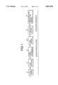
- FIG. 1 is a station diagram for the method according to the present invention
- FIG. 2 illustrates the extruded core after passing through the core sizing station
- FIG. 3 illustrates the core after passing through the core notching station
- FIG. 4 shows the core with the wire staple terminals attached
- FIG. 5 illustrates the core with the wire staple terminals and the wire windings
- FIG. 6 illustrates the inductors after passing through the inductor coating station
- FIG. 7 illustrates the separated inductors ready for testing and sorting
- FIG. 8 is an end view of the inductor according to the invention.
- FIG. 9 illustrates an alternative embodiment inductor according to the present invention.
- FIG. 1 is a station diagram for the method according to the invention.
- an extruded core material as shown in FIG. 2, with an arbitrary cross section (preferably rectangular) is fed into a core sizing station 12.
- the extruding process is well known and will not be further described.
- a core material such as a high temperature thermoplastic is extruded a length sufficient for a plurality of inductors.
- a high temperature thermoplastic is a thermoplastic having a melting temperature above about 350° F.
- a preferred material with respect to the present structure is a thermoplastic material having a melting temperature above about 650° F.
- thermoplastic core material can be extruded in large quantities and in a continuous process.
- the core material is readily machined for sizing and notching (described below). Any variation of the cross sectional area, the variable A in the above equation, corresponds directly to a variation in inductance value, the variable L in the above equation. Consequently, the core material can be machined to a desired cross section with extreme accuracy in accordance with a known machining process. Typically, the core material is machined to within a +/-0.0005" accuracy. A segment of machined core material is labeled 14 in FIG. 2.
- notches 18 are formed in the core material where the device terminals are to be placed.
- the notches 18 may be formed in any suitable manner, and are preferably formed with a solid carbide saw or a high speed steel saw.
- the notches 18 are formed on all sides of the core material in order to accommodate the device terminals, which are crimped around the device.
- the depth of each notch can be set and controlled with extreme accuracy. For example, a deeper notch is preferred on the top and sides of the inductor to minimize the inductor profile.
- the notch on the bottom conversely, can be made more shallow so that the height of the inductor above a printed circuit board can be controlled.
- a side view of a completed inductor illustrating the inductor profile is shown in FIG. 8.
- a segment of machined and notched core material is illustrated in FIG. 3.
- the inductor terminals 22 are added in the core staple attachment station 24.
- the inductor terminals 22 consist of wire staples that are formed from a coiled material and crimped around the core material at the notches 18.
- the staples are formed from spooled wire, such as 28 AWG tin-copper stock.
- the wire is sheared at an appropriate length, shaped to fit around the core using a first U-shaped tool, and crimped around the core using a second tool to form the device terminals.
- the second tool bends the U-shaped wire around the bottom of the core.
- a segment of core material having the wire staple terminals attached is shown in FIG. 4.
- the inductor windings 26 are added at a core winding station 28 by wrapping a fine gauge wire (typically 44 AWG) around the core material.
- the windings 26 are secured to the wire staple terminals 22 by any suitable method such as heat and pressure staking, extremely high temperature soldering, and welding. In the heat and pressure staking method, the windings 26 are heated and pressed against the wire staple terminal at any desired location.
- the windings 26 include a polyurethane insulator. When attaching the wire windings 26 to the wire staple terminals, the heat and pressure melts the polyurethane insulator and melts the tin of the wire staple.
- the melted tin flows around the inductor wire, thereby soldering the wire winding in place. Since the tin coating on the wire staple terminals create the bonding between the winding wire and the terminal staples, additional materials (such as solder) are not required.
- the wire staple terminals 22 are stapled around the core material, and thus, the wire windings 26 can be secured virtually anywhere along the perimeter of the inductor. As a result, the number of windings for the inductor can be finely controlled (including partial turns around the core), which enables the realization of intermediate inductance values for a given core size.
- the inductors are next passed through an inductor coating station 30 where a coating material 32 is dispensed between the two wire staple terminals 22 at the top of each inductor.
- the coating material 32 forms a smooth, flat surface that is well suited for automatic placement machines currently used in electrical circuit board assembly. Any suitable means of dispensing the coating material 32 could be used, and several such means are well-known. The details of the dispensing means will therefore not be further described.
- the coating material 32 is a UV curable material such as solder mask or dielectric coatings or one of various epoxies.
- the wire staple terminals 22 are spaced slightly above the top surface of the core to define a well 34 between the terminals. As a result of the well 34 defined by the terminals 22, an external mold is not required to form a uniform surface area for automated placement machines as is typically required with conventional inductors.
- the individual inductors 38 are separated from one another at the inductor cut-off, testing and sorting station 40.
- the inductors are mechanically sawed between the inductor terminals with sufficient room to allow for the kerf of the saw.
- the inductors can be separated using a known laser trimming process.
- the process according to the invention is a continuous process. Beginning with a spooled extruded material, inductors are formed on a core material sequentially. The inductors are not physically separated until the final stages of manufacturing (specifically for testing and sorting). This is in sharp contrast to the current method in which each inductor is individually constructed on an individual core that has been manufactured with tight tolerances and wound individually.
- the continuous process according to the invention establishes greater yields over a discrete process. Moreover, extruding the core material is a less expensive process as compared to molding that is used with thermoset plastics and ceramics.
- the process can maintain extremely tight tolerances (typically about 0.0005"), which is unprecedented in wire-wound inductor manufacturing.
- the ability to maintain such a high precision on the cross-sectional area results in highly controlled inductance values.
- the sizing process can be isolated from the inductor manufacturing process, and spool-to-spool machining operation can be performed at high speeds on the core material. Consequently, production volumes can be greatly enhanced.
- the wire winding process is also a continuous process with the spooled wire being rotated around the core material. This is in contrast to the prior method in which the individual inductors are rotated in a bobbin-like manner. Since the winding in the process according to the invention is continuous, manufacturing variations due to starting and stopping motions can be avoided. Moreover, less set up time is needed, and more inductors can be wound in a given time interval.
- the notching of the core material and forming staples out of spooled, standard tinned wire stock is an important feature of the invention.
- the terminal leads had to be formed in a secondary process (typically by plating with a high-temperature solder paste).
- additional material treatment such as heating to a high temperature and depositing the solder paste.
- manufacturing platforms are less costly.
- standard readily available materials are used instead of more complex materials that require special handling.
- the staple making process flattens the bottom of the wire stock, thus making it a better surface for soldering.
- the entire process can reside on a single manufacturing platform with a single positioning reference. Consequently, the input materials to each stage of the process do not have to be realigned. Instead, the entire stage (including notching, stapling, winding and cutting) is aligned to a single positioning reference.
- the prior method included several isolated manufacturing stages. As a result, each part needed to be carefully realigned in order to avoid large manufacturing deviations that may affect performance. As a result of the single manufacturing platform, a tighter manufacturing tolerance can be maintained that results in better yields. Moreover, since additional positioning devices for realignment are not required, manufacturing platforms are less costly. In similar regard, since the addition of a coating material is integrated into the manufacturing process, additional manufacturing steps are not required, and manufacturing platforms are less costly.
- the core can be extruded around a center conductor 45 to provide a magnetic core.
- the extrusion can have a slot in which a magnetic core can be later pressed.
Landscapes
- Engineering & Computer Science (AREA)
- Power Engineering (AREA)
- Manufacturing & Machinery (AREA)
- Coils Or Transformers For Communication (AREA)
- Manufacturing Cores, Coils, And Magnets (AREA)
Abstract
Description
Claims (28)
Priority Applications (11)
| Application Number | Priority Date | Filing Date | Title |
|---|---|---|---|
| US08/775,195 US5867891A (en) | 1996-12-30 | 1996-12-30 | Continuous method of manufacturing wire wound inductors and wire wound inductors thereby |
| MYPI97006091A MY119347A (en) | 1996-12-30 | 1997-12-17 | Continuous method of manufacturing wire wound inductors and wire wound inductors thereby. |
| BR9714111A BR9714111A (en) | 1996-12-30 | 1997-12-19 | Process for manufacturing inductors |
| DE69724281T DE69724281D1 (en) | 1996-12-30 | 1997-12-19 | CONTINUOUS METHOD FOR PRODUCING WIRE-WINDED INDUCTION COILS |
| EEP199900327A EE9900327A (en) | 1996-12-30 | 1997-12-19 | Method of continuous manufacture of wire inductors and wire inductors made by this method |
| EP97952559A EP0950251B1 (en) | 1996-12-30 | 1997-12-19 | Continuous method of manufacturing wire wound inductors |
| CNB971819718A CN1146928C (en) | 1996-12-30 | 1997-12-19 | Continuous method of mfg. wire wound inductors and wire wound inductors thereby |
| PCT/US1997/023559 WO1998029884A1 (en) | 1996-12-30 | 1997-12-19 | Continuous method of manufacturing wire wound inductors and wire wound inductors thereby |
| JP53012598A JP2001507865A (en) | 1996-12-30 | 1997-12-19 | Continuous manufacturing method of wound inductor and wound inductor manufactured by the method |
| AU56142/98A AU5614298A (en) | 1996-12-30 | 1997-12-19 | Continuous method of manufacturing wire wound inductors and wire wound inductorsthereby |
| HK00105756A HK1026506A1 (en) | 1996-12-30 | 2000-09-12 | Continuous method of manufacturing wire wound inductors. |
Applications Claiming Priority (1)
| Application Number | Priority Date | Filing Date | Title |
|---|---|---|---|
| US08/775,195 US5867891A (en) | 1996-12-30 | 1996-12-30 | Continuous method of manufacturing wire wound inductors and wire wound inductors thereby |
Publications (1)
| Publication Number | Publication Date |
|---|---|
| US5867891A true US5867891A (en) | 1999-02-09 |
Family
ID=25103624
Family Applications (1)
| Application Number | Title | Priority Date | Filing Date |
|---|---|---|---|
| US08/775,195 Expired - Lifetime US5867891A (en) | 1996-12-30 | 1996-12-30 | Continuous method of manufacturing wire wound inductors and wire wound inductors thereby |
Country Status (11)
| Country | Link |
|---|---|
| US (1) | US5867891A (en) |
| EP (1) | EP0950251B1 (en) |
| JP (1) | JP2001507865A (en) |
| CN (1) | CN1146928C (en) |
| AU (1) | AU5614298A (en) |
| BR (1) | BR9714111A (en) |
| DE (1) | DE69724281D1 (en) |
| EE (1) | EE9900327A (en) |
| HK (1) | HK1026506A1 (en) |
| MY (1) | MY119347A (en) |
| WO (1) | WO1998029884A1 (en) |
Cited By (13)
| Publication number | Priority date | Publication date | Assignee | Title |
|---|---|---|---|---|
| USRE39453E1 (en) | 1999-10-28 | 2007-01-02 | Coilcraft, Incorporated | Low profile inductive component |
| US20090055022A1 (en) * | 2000-01-24 | 2009-02-26 | Irobot Corporation | Obstacle following sensor scheme for a mobile robot |
| US20090058590A1 (en) * | 2005-05-13 | 2009-03-05 | Rupert Aumueller | Electronic component and method for fixing the same |
| US20110005064A1 (en) * | 2006-08-09 | 2011-01-13 | Coilcraft, Incorporated | Method of manufacturing an electronic component |
| US20110163833A1 (en) * | 2008-06-24 | 2011-07-07 | S e r g e y P u l n i k o v | Method for making electrical windings for electrical apparatus and transformers and windings obtained by said method |
| US20130335186A1 (en) * | 2012-04-24 | 2013-12-19 | Cyntec Co., Ltd. | Electromagnetic component and fabrication method thereof |
| US8731687B2 (en) | 2009-03-04 | 2014-05-20 | Imricor Medical Systems, Inc. | Method of constructing MRI compatible electrode circuit |
| US8761899B2 (en) | 2009-03-04 | 2014-06-24 | Imricor Medical Systems, Inc. | MRI compatible conductive wires |
| US8805540B2 (en) | 2009-03-04 | 2014-08-12 | Imricor Medical Systems, Inc. | MRI compatible cable |
| US8831743B2 (en) | 2009-03-04 | 2014-09-09 | Imricor Medical Systems, Inc. | MRI compatible electrode circuit |
| US8843213B2 (en) | 2009-03-04 | 2014-09-23 | Imricor Medical Systems, Inc. | MRI compatible co-radially wound lead assembly |
| US8855788B2 (en) | 2009-03-04 | 2014-10-07 | Imricor Medical Systems, Inc. | MRI compatible electrode circuit |
| US20160172942A1 (en) * | 2013-07-04 | 2016-06-16 | Linak A/S | Actuator system |
Families Citing this family (2)
| Publication number | Priority date | Publication date | Assignee | Title |
|---|---|---|---|---|
| JP4548110B2 (en) * | 2004-12-13 | 2010-09-22 | パナソニック株式会社 | Manufacturing method of chip parts |
| CN110335749B (en) * | 2019-07-27 | 2021-06-15 | 东莞市慧研自动化设备科技有限公司 | Automatic winding and foot winding equipment and method for SQ common mode inductor |
Citations (27)
| Publication number | Priority date | Publication date | Assignee | Title |
|---|---|---|---|---|
| US2298275A (en) * | 1940-08-31 | 1942-10-13 | Bell Telephone Labor Inc | Electrical coil |
| US3196523A (en) * | 1958-06-30 | 1965-07-27 | Zenith Radio Corp | Method of constructing a tuning strip |
| US3259862A (en) * | 1963-05-27 | 1966-07-05 | Kenneth L Richard | Tunable electronic component |
| US3323200A (en) * | 1964-05-19 | 1967-06-06 | Automatic Elect Lab | Method for manufacturing selfsupporting coils |
| US3367816A (en) * | 1963-12-27 | 1968-02-06 | Stone Straw Corp | Method of helically winding coil forms while extruding material onto the inner wall |
| US3609833A (en) * | 1968-10-14 | 1971-10-05 | Lucas Industries Ltd | Method of making ignition coils |
| US3659336A (en) * | 1970-01-30 | 1972-05-02 | Electronic Diversified Inc | Method of manufacturing an inductive device |
| DE2055285A1 (en) * | 1970-11-10 | 1972-05-25 | Rhein Westfael Isolatoren | Process for wrapping wire resistors Process for wrapping wire resistors |
| US3670406A (en) * | 1970-02-04 | 1972-06-20 | Texas Instruments Inc | Method of adjusting inductive devices |
| US3684993A (en) * | 1971-02-18 | 1972-08-15 | Bell Telephone Labor Inc | Variable inductance coil form assembly |
| US3689981A (en) * | 1971-08-13 | 1972-09-12 | Western Electric Co | Methods of assembling electrical components |
| US3811045A (en) * | 1972-04-19 | 1974-05-14 | Magnetic Labor Inc | Coil manufacturing process |
| DE2450513A1 (en) * | 1974-10-24 | 1976-04-29 | Standard Elektrik Lorenz Ag | Choke assembly with two coils on one core - has insulation separator between coils |
| DE3042433A1 (en) * | 1980-11-11 | 1982-07-01 | Draloric Electronic GmbH, 8500 Nürnberg | Inductive component for printed circuit mounting - has ends of wire coil wound round cylindrical central portion, and electrically coupled to both metal films on end blocks |
| JPS57211712A (en) * | 1981-06-23 | 1982-12-25 | Matsushita Electric Ind Co Ltd | Multiplex winding method |
| JPS5875825A (en) * | 1981-10-29 | 1983-05-07 | Murata Mfg Co Ltd | Manufacture of chip inductor |
| US4516103A (en) * | 1983-05-17 | 1985-05-07 | Meteor Ag | Plug-in arrangement and process for tin plating contacts of a plug-in arrangement |
| US4621251A (en) * | 1985-03-28 | 1986-11-04 | North American Philips Corp. | Electric resistance heater assembly |
| US4696100A (en) * | 1985-02-21 | 1987-09-29 | Matsushita Electric Industrial Co., Ltd. | Method of manufacturing a chip coil |
| US4785527A (en) * | 1986-01-21 | 1988-11-22 | Compagnie Europeenne De Composants Electroniques Lcc | Method for manufacturing an inductive chip |
| JPH02271511A (en) * | 1989-04-12 | 1990-11-06 | Toko Inc | Manufacture of chip-type inductor |
| JPH02290006A (en) * | 1990-04-06 | 1990-11-29 | Tokin Corp | Manufacture of inductance element |
| US5191701A (en) * | 1990-12-11 | 1993-03-09 | Siemens Matsushita Comp. Gmbh & Co. Kg | Method for the automated manufacture of wound electrical components by contacting thin insulated wires to terminal elements on the basis of laser welding |
| US5262745A (en) * | 1992-01-27 | 1993-11-16 | Pulse Engineering, Inc. | Surface mounted multi-section bobbin |
| US5351167A (en) * | 1992-01-24 | 1994-09-27 | Pulse Engineering, Inc. | Self-leaded surface mounted rod inductor |
| US5572788A (en) * | 1992-07-30 | 1996-11-12 | Tdk Corporation | Coil device |
| US5692290A (en) * | 1994-09-19 | 1997-12-02 | Taiyo Yuden Kabushiki Kaisha | Method of manufacturing a chip inductor |
-
1996
- 1996-12-30 US US08/775,195 patent/US5867891A/en not_active Expired - Lifetime
-
1997
- 1997-12-17 MY MYPI97006091A patent/MY119347A/en unknown
- 1997-12-19 JP JP53012598A patent/JP2001507865A/en active Pending
- 1997-12-19 BR BR9714111A patent/BR9714111A/en not_active IP Right Cessation
- 1997-12-19 DE DE69724281T patent/DE69724281D1/en not_active Expired - Lifetime
- 1997-12-19 EP EP97952559A patent/EP0950251B1/en not_active Expired - Lifetime
- 1997-12-19 WO PCT/US1997/023559 patent/WO1998029884A1/en active IP Right Grant
- 1997-12-19 EE EEP199900327A patent/EE9900327A/en unknown
- 1997-12-19 CN CNB971819718A patent/CN1146928C/en not_active Expired - Fee Related
- 1997-12-19 AU AU56142/98A patent/AU5614298A/en not_active Abandoned
-
2000
- 2000-09-12 HK HK00105756A patent/HK1026506A1/en not_active IP Right Cessation
Patent Citations (27)
| Publication number | Priority date | Publication date | Assignee | Title |
|---|---|---|---|---|
| US2298275A (en) * | 1940-08-31 | 1942-10-13 | Bell Telephone Labor Inc | Electrical coil |
| US3196523A (en) * | 1958-06-30 | 1965-07-27 | Zenith Radio Corp | Method of constructing a tuning strip |
| US3259862A (en) * | 1963-05-27 | 1966-07-05 | Kenneth L Richard | Tunable electronic component |
| US3367816A (en) * | 1963-12-27 | 1968-02-06 | Stone Straw Corp | Method of helically winding coil forms while extruding material onto the inner wall |
| US3323200A (en) * | 1964-05-19 | 1967-06-06 | Automatic Elect Lab | Method for manufacturing selfsupporting coils |
| US3609833A (en) * | 1968-10-14 | 1971-10-05 | Lucas Industries Ltd | Method of making ignition coils |
| US3659336A (en) * | 1970-01-30 | 1972-05-02 | Electronic Diversified Inc | Method of manufacturing an inductive device |
| US3670406A (en) * | 1970-02-04 | 1972-06-20 | Texas Instruments Inc | Method of adjusting inductive devices |
| DE2055285A1 (en) * | 1970-11-10 | 1972-05-25 | Rhein Westfael Isolatoren | Process for wrapping wire resistors Process for wrapping wire resistors |
| US3684993A (en) * | 1971-02-18 | 1972-08-15 | Bell Telephone Labor Inc | Variable inductance coil form assembly |
| US3689981A (en) * | 1971-08-13 | 1972-09-12 | Western Electric Co | Methods of assembling electrical components |
| US3811045A (en) * | 1972-04-19 | 1974-05-14 | Magnetic Labor Inc | Coil manufacturing process |
| DE2450513A1 (en) * | 1974-10-24 | 1976-04-29 | Standard Elektrik Lorenz Ag | Choke assembly with two coils on one core - has insulation separator between coils |
| DE3042433A1 (en) * | 1980-11-11 | 1982-07-01 | Draloric Electronic GmbH, 8500 Nürnberg | Inductive component for printed circuit mounting - has ends of wire coil wound round cylindrical central portion, and electrically coupled to both metal films on end blocks |
| JPS57211712A (en) * | 1981-06-23 | 1982-12-25 | Matsushita Electric Ind Co Ltd | Multiplex winding method |
| JPS5875825A (en) * | 1981-10-29 | 1983-05-07 | Murata Mfg Co Ltd | Manufacture of chip inductor |
| US4516103A (en) * | 1983-05-17 | 1985-05-07 | Meteor Ag | Plug-in arrangement and process for tin plating contacts of a plug-in arrangement |
| US4696100A (en) * | 1985-02-21 | 1987-09-29 | Matsushita Electric Industrial Co., Ltd. | Method of manufacturing a chip coil |
| US4621251A (en) * | 1985-03-28 | 1986-11-04 | North American Philips Corp. | Electric resistance heater assembly |
| US4785527A (en) * | 1986-01-21 | 1988-11-22 | Compagnie Europeenne De Composants Electroniques Lcc | Method for manufacturing an inductive chip |
| JPH02271511A (en) * | 1989-04-12 | 1990-11-06 | Toko Inc | Manufacture of chip-type inductor |
| JPH02290006A (en) * | 1990-04-06 | 1990-11-29 | Tokin Corp | Manufacture of inductance element |
| US5191701A (en) * | 1990-12-11 | 1993-03-09 | Siemens Matsushita Comp. Gmbh & Co. Kg | Method for the automated manufacture of wound electrical components by contacting thin insulated wires to terminal elements on the basis of laser welding |
| US5351167A (en) * | 1992-01-24 | 1994-09-27 | Pulse Engineering, Inc. | Self-leaded surface mounted rod inductor |
| US5262745A (en) * | 1992-01-27 | 1993-11-16 | Pulse Engineering, Inc. | Surface mounted multi-section bobbin |
| US5572788A (en) * | 1992-07-30 | 1996-11-12 | Tdk Corporation | Coil device |
| US5692290A (en) * | 1994-09-19 | 1997-12-02 | Taiyo Yuden Kabushiki Kaisha | Method of manufacturing a chip inductor |
Non-Patent Citations (6)
| Title |
|---|
| ATT Technologies, Technical Digest , No. 76, Mar. 1985, F. T. Dickens and R. A. Frantz, Jr., pp. 19 and 20. * |
| ATT Technologies, Technical Digest, No. 76, Mar. 1985, F. T. Dickens and R. A. Frantz, Jr., pp. 19 and 20. |
| Patent Abstracts of Japan, vol. 007, No. 065 (E 165), 18 Mar. 1983 & JP 57 211712 A (Matsushita Denki Sangyo KK), 25 Dec. 1982, see abstract. * |
| Patent Abstracts of Japan, vol. 007, No. 065 (E-165), 18 Mar. 1983 & JP 57 211712 A (Matsushita Denki Sangyo KK), 25 Dec. 1982, see abstract. |
| Patent Abstracts of Japan, vol. 007, No. 170 (E 189), 27 Jul. 1983 & JP 58 075825 A (Murata Seisakusho:KK), 7 May 1983, see abstract. * |
| Patent Abstracts of Japan, vol. 007, No. 170 (E-189), 27 Jul. 1983 & JP 58 075825 A (Murata Seisakusho:KK), 7 May 1983, see abstract. |
Cited By (21)
| Publication number | Priority date | Publication date | Assignee | Title |
|---|---|---|---|---|
| USRE39453E1 (en) | 1999-10-28 | 2007-01-02 | Coilcraft, Incorporated | Low profile inductive component |
| US20090055022A1 (en) * | 2000-01-24 | 2009-02-26 | Irobot Corporation | Obstacle following sensor scheme for a mobile robot |
| US20090058590A1 (en) * | 2005-05-13 | 2009-03-05 | Rupert Aumueller | Electronic component and method for fixing the same |
| US7973634B2 (en) | 2005-05-13 | 2011-07-05 | Wuerth Elektronik Ibe Gmbh | Electronic component and method for fixing the same |
| US20110005064A1 (en) * | 2006-08-09 | 2011-01-13 | Coilcraft, Incorporated | Method of manufacturing an electronic component |
| US11869696B2 (en) | 2006-08-09 | 2024-01-09 | Coilcraft, Incorporated | Electronic component |
| US10319507B2 (en) | 2006-08-09 | 2019-06-11 | Coilcraft, Incorporated | Method of manufacturing an electronic component |
| US9318251B2 (en) * | 2006-08-09 | 2016-04-19 | Coilcraft, Incorporated | Method of manufacturing an electronic component |
| US20110163833A1 (en) * | 2008-06-24 | 2011-07-07 | S e r g e y P u l n i k o v | Method for making electrical windings for electrical apparatus and transformers and windings obtained by said method |
| US8316528B2 (en) * | 2008-06-24 | 2012-11-27 | Sergey Pulnikov | Method for making electrical windings for transformers and electrical apparatus |
| US8761900B2 (en) | 2009-03-04 | 2014-06-24 | Imricor Medical Systems, Inc. | MRI compatible electrode circuit |
| US8805540B2 (en) | 2009-03-04 | 2014-08-12 | Imricor Medical Systems, Inc. | MRI compatible cable |
| US8831743B2 (en) | 2009-03-04 | 2014-09-09 | Imricor Medical Systems, Inc. | MRI compatible electrode circuit |
| US8843212B2 (en) | 2009-03-04 | 2014-09-23 | Imricor Medical Systems, Inc. | MRI compatible co-radially wound lead assembly |
| US8843213B2 (en) | 2009-03-04 | 2014-09-23 | Imricor Medical Systems, Inc. | MRI compatible co-radially wound lead assembly |
| US8855788B2 (en) | 2009-03-04 | 2014-10-07 | Imricor Medical Systems, Inc. | MRI compatible electrode circuit |
| US8761899B2 (en) | 2009-03-04 | 2014-06-24 | Imricor Medical Systems, Inc. | MRI compatible conductive wires |
| US8731687B2 (en) | 2009-03-04 | 2014-05-20 | Imricor Medical Systems, Inc. | Method of constructing MRI compatible electrode circuit |
| US9009951B2 (en) * | 2012-04-24 | 2015-04-21 | Cyntec Co., Ltd. | Method of fabricating an electromagnetic component |
| US20130335186A1 (en) * | 2012-04-24 | 2013-12-19 | Cyntec Co., Ltd. | Electromagnetic component and fabrication method thereof |
| US20160172942A1 (en) * | 2013-07-04 | 2016-06-16 | Linak A/S | Actuator system |
Also Published As
| Publication number | Publication date |
|---|---|
| CN1247631A (en) | 2000-03-15 |
| HK1026506A1 (en) | 2000-12-15 |
| DE69724281D1 (en) | 2003-09-25 |
| EP0950251B1 (en) | 2003-08-20 |
| EP0950251A1 (en) | 1999-10-20 |
| WO1998029884A1 (en) | 1998-07-09 |
| AU5614298A (en) | 1998-07-31 |
| MY119347A (en) | 2005-05-31 |
| EE9900327A (en) | 2000-02-15 |
| JP2001507865A (en) | 2001-06-12 |
| CN1146928C (en) | 2004-04-21 |
| BR9714111A (en) | 2000-03-21 |
Similar Documents
| Publication | Publication Date | Title |
|---|---|---|
| US5867891A (en) | Continuous method of manufacturing wire wound inductors and wire wound inductors thereby | |
| US5903207A (en) | Wire wound inductors | |
| CA2163052C (en) | Low profile inductor/transformer component | |
| US6842101B2 (en) | Tunable inductor | |
| US6087921A (en) | Placement insensitive monolithic inductor and method of manufacturing same | |
| US5692290A (en) | Method of manufacturing a chip inductor | |
| US4333069A (en) | Electrical resistor for a printed circuit board and method of making the same | |
| US4878291A (en) | Method of manufacturing toroidal coils | |
| US3534309A (en) | Mount for circuit elements | |
| US3743990A (en) | An inductor with mounting means | |
| KR920005350B1 (en) | Semiconductor component with two connections and process and device for manufacturing it | |
| US5232463A (en) | Apparatus for manufacturing a semiconductor device | |
| EP1647999B1 (en) | A mounting assembly for inductors and method of producing the same | |
| SU936059A1 (en) | Method of manufacturing flat spiral inductance coils | |
| JP2787592B2 (en) | Bead inductor and manufacturing method thereof | |
| JPS6123307A (en) | Pin terminal in parts of electric winding | |
| JP3049201U (en) | Bobbins and chip inductors for wound chip components | |
| JPH0369103A (en) | Chip-type coil and manufacture thereof | |
| JPH0748439B2 (en) | Inductor manufacturing method | |
| JPH05217752A (en) | Chip inductor and manufacture of the same | |
| JPH05182855A (en) | Manufacture of choke coil | |
| JPH04346403A (en) | Constitution of wire-wound chip inductor and manufacture thereof | |
| JPH0195508A (en) | Manufacture of chip type coil | |
| JPH08186026A (en) | High-frequency coil and manufacture thereof | |
| JPH0581044B2 (en) |
Legal Events
| Date | Code | Title | Description |
|---|---|---|---|
| AS | Assignment |
Owner name: ERICSSON INC., A DELAWARE CORPORATION, NORTH CARO Free format text: ASSIGNMENT OF ASSIGNORS INTEREST;ASSIGNORS:LAMPE, ROSS WARREN;HAYES, GERARD JAMES;REEL/FRAME:008377/0763 Effective date: 19961223 |
|
| STCF | Information on status: patent grant |
Free format text: PATENTED CASE |
|
| FEPP | Fee payment procedure |
Free format text: PAYOR NUMBER ASSIGNED (ORIGINAL EVENT CODE: ASPN); ENTITY STATUS OF PATENT OWNER: LARGE ENTITY |
|
| FPAY | Fee payment |
Year of fee payment: 4 |
|
| REMI | Maintenance fee reminder mailed | ||
| FPAY | Fee payment |
Year of fee payment: 8 |
|
| FPAY | Fee payment |
Year of fee payment: 12 |
|
| AS | Assignment |
Owner name: RESEARCH IN MOTION LIMITED, CANADA Free format text: ASSIGNMENT OF ASSIGNORS INTEREST;ASSIGNOR:TELEFONAKTIEBOLAGET L M ERICSSON (PUBL);REEL/FRAME:026251/0104 Effective date: 20110325 |
|
| AS | Assignment |
Owner name: BLACKBERRY LIMITED, ONTARIO Free format text: CHANGE OF NAME;ASSIGNOR:RESEARCH IN MOTION LIMITED;REEL/FRAME:038025/0078 Effective date: 20130709 |