JP5926955B2 - Imaging mechanism and endoscope apparatus - Google Patents
Imaging mechanism and endoscope apparatus Download PDFInfo
- Publication number
- JP5926955B2 JP5926955B2 JP2011289349A JP2011289349A JP5926955B2 JP 5926955 B2 JP5926955 B2 JP 5926955B2 JP 2011289349 A JP2011289349 A JP 2011289349A JP 2011289349 A JP2011289349 A JP 2011289349A JP 5926955 B2 JP5926955 B2 JP 5926955B2
- Authority
- JP
- Japan
- Prior art keywords
- sensor
- contact
- circuit board
- holding member
- image sensor
- Prior art date
- Legal status (The legal status is an assumption and is not a legal conclusion. Google has not performed a legal analysis and makes no representation as to the accuracy of the status listed.)
- Expired - Fee Related
Links
- 238000003384 imaging method Methods 0.000 title claims description 62
- 238000003780 insertion Methods 0.000 claims description 37
- 230000037431 insertion Effects 0.000 claims description 37
- 239000004020 conductor Substances 0.000 claims description 13
- 239000002184 metal Substances 0.000 claims description 11
- 230000003287 optical effect Effects 0.000 description 18
- 238000005452 bending Methods 0.000 description 16
- 238000005286 illumination Methods 0.000 description 14
- 239000000758 substrate Substances 0.000 description 7
- 239000011295 pitch Substances 0.000 description 4
- 238000005476 soldering Methods 0.000 description 4
- 239000011347 resin Substances 0.000 description 3
- 229920005989 resin Polymers 0.000 description 3
- 239000010409 thin film Substances 0.000 description 3
- 239000000463 material Substances 0.000 description 2
- 239000000853 adhesive Substances 0.000 description 1
- 230000001070 adhesive effect Effects 0.000 description 1
- 239000000919 ceramic Substances 0.000 description 1
- 239000000470 constituent Substances 0.000 description 1
- 230000007423 decrease Effects 0.000 description 1
- 239000004519 grease Substances 0.000 description 1
- 230000017525 heat dissipation Effects 0.000 description 1
- 230000020169 heat generation Effects 0.000 description 1
- 239000011810 insulating material Substances 0.000 description 1
- 238000009413 insulation Methods 0.000 description 1
- 230000010354 integration Effects 0.000 description 1
- 239000004973 liquid crystal related substance Substances 0.000 description 1
- 230000007935 neutral effect Effects 0.000 description 1
- 230000002093 peripheral effect Effects 0.000 description 1
- 230000005855 radiation Effects 0.000 description 1
- 229910000679 solder Inorganic materials 0.000 description 1
Images


Classifications
-
- A—HUMAN NECESSITIES
- A61—MEDICAL OR VETERINARY SCIENCE; HYGIENE
- A61B—DIAGNOSIS; SURGERY; IDENTIFICATION
- A61B1/00—Instruments for performing medical examinations of the interior of cavities or tubes of the body by visual or photographical inspection, e.g. endoscopes; Illuminating arrangements therefor
- A61B1/04—Instruments for performing medical examinations of the interior of cavities or tubes of the body by visual or photographical inspection, e.g. endoscopes; Illuminating arrangements therefor combined with photographic or television appliances
- A61B1/05—Instruments for performing medical examinations of the interior of cavities or tubes of the body by visual or photographical inspection, e.g. endoscopes; Illuminating arrangements therefor combined with photographic or television appliances characterised by the image sensor, e.g. camera, being in the distal end portion
- A61B1/051—Details of CCD assembly
Description
本発明は、撮像機構及び内視鏡装置に関する。 The present invention relates to an imaging mechanism and an endoscope apparatus.
従来、観察対象物の内部等を観察する際に、内視鏡装置を観察対象物の内部等に挿入して観察することが知られている。内視鏡装置としては、例えば遠位端と近位端とを有する長尺の挿入部を備え、挿入部の遠位端に対象物を撮像するための撮像機構が配置されたものが知られている。 Conventionally, when observing the inside or the like of an observation object, it is known to insert an endoscope apparatus into the observation object or the like for observation. As an endoscope apparatus, for example, an endoscope apparatus having a long insertion portion having a distal end and a proximal end, and an imaging mechanism for imaging an object at the distal end of the insertion portion is known. ing.
このような撮像機構の例として、たとえば特許文献1には、電子内視鏡の先端部が開示されている。特許文献1に記載の電子内視鏡は、先端部において、固体撮像素子(イメージセンサ)が実装された基板とイメージセンサに電気的に接続された信号線とが樹脂塊内に封止されている。
特許文献1に記載の電子内視鏡の先端部において、上記樹脂塊は硬質であるので、樹脂塊が設けられた部分は、柔軟性に乏しい硬質部となっている。ここで、イメージセンサに電気的に接続された信号線の先端から各信号線が一束となる部分までの間も上記硬質部となっている。
As an example of such an imaging mechanism, for example, Patent Document 1 discloses a distal end portion of an electronic endoscope. In the electronic endoscope described in Patent Document 1, a substrate on which a solid-state imaging device (image sensor) is mounted and a signal line electrically connected to the image sensor are sealed in a resin block at the distal end. Yes.
In the distal end portion of the electronic endoscope described in Patent Document 1, since the resin mass is hard, the portion provided with the resin mass is a hard portion that is poor in flexibility. Here, the portion from the tip of the signal line electrically connected to the image sensor to the portion where each signal line is bundled is also the hard portion.
近年、受光素子数が多いイメージセンサが知られている。このようなイメージセンサは、多数の受光素子が整列して形成されたセンサ面を有しており、センサ面の面積を大きく取って受光素子数を増やしたものや、受光素子の集積度を上げ受光素子ピッチを小さくすることにより受光素子数を増やしたものなどが知られている。ここで、受光素子ピッチが小さすぎると、受光素子数を多くしてもイメージセンサによって得られた画像の画質を向上させにくいという問題があり、高画質の画像を撮像するイメージセンサは、センサ面の面積が大きくなる傾向がある。 In recent years, image sensors having a large number of light receiving elements are known. Such an image sensor has a sensor surface in which a large number of light receiving elements are aligned, and increases the number of light receiving elements by increasing the area of the sensor surface, and increases the degree of integration of the light receiving elements. A device in which the number of light receiving elements is increased by reducing the light receiving element pitch is known. Here, if the pitch of the light receiving elements is too small, there is a problem that it is difficult to improve the image quality of the image obtained by the image sensor even if the number of light receiving elements is increased. The area tends to increase.
また、内視鏡装置には、細い隙間等に挿入しやすい細径で柔軟な挿入部が求められている。しかしながら、従来の内視鏡装置は、挿入部内に搭載可能なイメージセンサを高画質で大型なものとしようとすると、イメージセンサに接続する信号線等を含む硬質部の寸法も大きくなり、挿入部が大径となったり挿入部の硬質部の長さが長くなったりするという課題を抱えている。 Further, an endoscope apparatus is required to have a thin and flexible insertion portion that can be easily inserted into a narrow gap or the like. However, in the conventional endoscope apparatus, if the image sensor that can be mounted in the insertion portion is to be large in size with high image quality, the size of the hard portion including the signal line connected to the image sensor also increases, and the insertion portion Has a problem that the diameter becomes large or the length of the hard part of the insertion part becomes long.
本発明は、上述した事情に鑑みてなされたものであって、その目的は、高画質のイメージセンサを搭載しても挿入部の大型化を抑えることができる撮像機構及び内視鏡装置を提供することである。 The present invention has been made in view of the above-described circumstances, and an object thereof is to provide an imaging mechanism and an endoscope apparatus that can suppress an increase in size of an insertion portion even when a high-quality image sensor is mounted. It is to be.
上記課題を解決するために、この発明は以下の手段を提案している。
本発明の第一の態様は、複数の受光素子が配されたセンサ面と複数の入出力用リードとを有するイメージセンサと、前記イメージセンサにおいて前記センサ面が設けられた側とは反対側の面に接するセンサ接触面を有する保持部材と、前記保持部材における前記センサ接触面と反対側の外面に固定され、前記センサ面と平行な実装面を有し、前記実装面に垂直な方向から見たときに輪郭線の少なくとも一部が前記保持部材の輪郭線の内側に位置する回路基板と、前記回路基板において前記実装面と交差して形成された側面上であって前記回路基板の輪郭線が前記保持部材の輪郭線の内側に位置している領域内に配された接点部と、を備え、前記保持部材と前記回路基板との少なくともいずれかは、前記接点部が電気的に接続されているとともに前記入出力用リードの少なくとも一つが電気的に接続された中継配線部を有し、前記接点部には、前記イメージセンサに対して電力若しくは電気信号を伝送するための第一配線が接続され、前記側面のうち前記接点部が配された面とは異なる面上には、前記入出力用リードの少なくとも他の一つが接続され且つ前記イメージセンサに対して電力若しくは電気信号を伝送するための第二配線が接続される第二接点部が設けられており、前記第一配線のうちの少なくとも一つは前記第二配線よりも外径が太いことを特徴とする撮像機構である。
In order to solve the above problems, the present invention proposes the following means.
According to a first aspect of the present invention, there is provided an image sensor having a sensor surface on which a plurality of light receiving elements are arranged and a plurality of input / output leads, and a side of the image sensor opposite to the side on which the sensor surface is provided. A holding member having a sensor contact surface in contact with the surface, and a mounting surface fixed to the outer surface of the holding member opposite to the sensor contact surface, having a mounting surface parallel to the sensor surface, and viewed from a direction perpendicular to the mounting surface. A circuit board in which at least a part of the contour line is positioned inside the contour line of the holding member, and a side surface formed on the circuit board so as to intersect the mounting surface, and the contour line of the circuit board Is disposed in a region located inside the contour line of the holding member, and at least one of the holding member and the circuit board is electrically connected to the contact portion. With Wherein at least one of the input-output lead has a relay wiring section electrically connected to said contact portion, a first wiring for transmitting the electrical power or electrical signals to the image sensor is connected, At least one other of the input / output leads is connected to a surface different from the surface on which the contact portion is disposed among the side surfaces, and a power or electric signal is transmitted to the image sensor. A second contact portion to which two wires are connected is provided, and at least one of the first wires has an outer diameter larger than that of the second wire .
本発明の第二の態様は、複数の受光素子が配されたセンサ面と複数の入出力用リードとを有するイメージセンサと、前記イメージセンサにおいて前記センサ面が設けられた側とは反対側の面に接するセンサ接触面を有する保持部材と、前記保持部材における前記センサ接触面と反対側の外面に固定され、前記センサ面と平行な実装面を有し、前記実装面に垂直な方向から見たときに輪郭線の少なくとも一部が前記保持部材の輪郭線の内側に位置する回路基板と、前記回路基板において前記実装面と交差して形成された側面上であって前記回路基板の輪郭線が前記保持部材の輪郭線の内側に位置している領域内に配された接点部と、を備え、前記保持部材と前記回路基板との少なくともいずれかは、前記接点部が電気的に接続されているとともに前記入出力用リードの少なくとも一つが電気的に接続された中継配線部を有し、前記側面のうち前記接点部が配された面とは異なる面上には、前記入出力用リードの少なくとも他の一つが接続され且つ前記イメージセンサに対して電力若しくは電気信号を伝送するための第二配線が接続される第二接点部が設けられており、前記領域内には、前記接点部と異なる第三接点部が配され、前記第三接点部は、前記回路基板に設けられた導体パターンと接続され、前記回路基板上に実装された電子部品と電気的に接続され、前記第三接点部には、前記電子部品と前記イメージセンサとの少なくともいずれかに対して電力若しくは電気信号を伝送するための第三配線が電気的且つ機械的に接続されることを特徴とする撮像機構である。 According to a second aspect of the present invention, there is provided an image sensor having a sensor surface on which a plurality of light receiving elements are arranged and a plurality of input / output leads, and a side opposite to the side on which the sensor surface is provided in the image sensor. A holding member having a sensor contact surface in contact with the surface, and a mounting surface fixed to the outer surface of the holding member opposite to the sensor contact surface, having a mounting surface parallel to the sensor surface, and viewed from a direction perpendicular to the mounting surface. A circuit board in which at least a part of the contour line is positioned inside the contour line of the holding member, and a side surface formed on the circuit board so as to intersect the mounting surface, and the contour line of the circuit board Is disposed in a region located inside the contour line of the holding member, and at least one of the holding member and the circuit board is electrically connected to the contact portion. With At least one of the input / output leads has a relay wiring portion electrically connected to at least one of the input / output leads, and the other side of the side surface is different from the surface on which the contact portion is disposed. And a second contact portion to which a second wiring for transmitting electric power or an electric signal to the image sensor is connected. A second contact portion different from the contact portion is provided in the region. Three contact portions are arranged, the third contact portion is connected to a conductor pattern provided on the circuit board, is electrically connected to an electronic component mounted on the circuit board, and is connected to the third contact portion. The image pickup mechanism is characterized in that a third wiring for transmitting electric power or an electric signal is electrically and mechanically connected to at least one of the electronic component and the image sensor.
また、前記第三接点部は1つ以上設けられていてもよく、前記第三接点部に接続された前記第三配線のうちの少なくとも一つは前記第二配線よりも外径が太くてもよい。 One or more of the third contact portions may be provided, and at least one of the third wirings connected to the third contact portion may have a larger outer diameter than the second wiring. Good.
本発明の第三の態様は、複数の受光素子が配されたセンサ面と複数の入出力用リードとを有するイメージセンサと、前記イメージセンサにおいて前記センサ面が設けられた側とは反対側の面に接するセンサ接触面を有する保持部材と、前記保持部材における前記センサ接触面と反対側の外面に固定され、前記センサ面と平行な実装面を有し、前記実装面に垂直な方向から見たときに輪郭線の少なくとも一部が前記保持部材の輪郭線の内側に位置する回路基板と、前記回路基板において前記実装面と交差して形成された側面上であって前記回路基板の輪郭線が前記保持部材の輪郭線の内側に位置している領域内に配された接点部と、を備え、前記保持部材と前記回路基板との少なくともいずれかは、前記接点部が電気的に接続されているとともに前記入出力用リードの少なくとも一つが電気的に接続された中継配線部を有し、前記回路基板の実装面には、前記実装面と平行な外面を有する電子部品が実装され、前記回路基板には、前記電子部品を覆い熱伝導性を有する絶縁性のカバーが固定され、前記電子部品の前記外面と前記カバーとの間には、熱伝導性を有する絶縁性の熱伝導シートが介在されていることを特徴とする撮像機構である。 According to a third aspect of the present invention, there is provided an image sensor having a sensor surface on which a plurality of light receiving elements are arranged and a plurality of input / output leads, and a side of the image sensor opposite to the side on which the sensor surface is provided. A holding member having a sensor contact surface in contact with the surface, and a mounting surface fixed to the outer surface of the holding member opposite to the sensor contact surface, having a mounting surface parallel to the sensor surface, and viewed from a direction perpendicular to the mounting surface. A circuit board in which at least a part of the contour line is positioned inside the contour line of the holding member, and a side surface formed on the circuit board so as to intersect the mounting surface, and the contour line of the circuit board Is disposed in a region located inside the contour line of the holding member, and at least one of the holding member and the circuit board is electrically connected to the contact portion. With An electronic component having an outer surface parallel to the mounting surface is mounted on the mounting surface of the circuit board, and at least one of the input / output leads is electrically connected. An insulating cover having heat conductivity covering the electronic component is fixed, and an insulating heat conductive sheet having heat conductivity is interposed between the outer surface of the electronic component and the cover. It is an imaging mechanism characterized by having.
前記カバーは、前記実装面に垂直な軸線回りに測った長さが、前記実装面に近い側の端における前記長さよりも、前記実装面から遠い側の端における前記長さの方が短くてもよい。 The cover has a length measured about an axis perpendicular to the mounting surface, and the length at the end far from the mounting surface is shorter than the length at the end near the mounting surface. Also good.
前記接点部は、複数設けられ、前記接点部には、イメージセンサに対して電力若しくは電気信号を伝送するための第一配線が接続され、前記第三接点部は、前記複数の接点部の間に設けられ、前記第三接点部に接続された前記第三配線のうちの少なくとも一つは、前記第一配線よりも外径が太くてもよい。 A plurality of the contact portions are provided, a first wiring for transmitting power or an electric signal to the image sensor is connected to the contact portions, and the third contact portion is between the plurality of contact portions. And at least one of the third wirings connected to the third contact portion may have a larger outer diameter than the first wiring.
本発明の第四の態様は、複数の受光素子が配されたセンサ面と複数の入出力用リードとを有するイメージセンサと、前記イメージセンサにおいて前記センサ面が設けられた側とは反対側の面に接するセンサ接触面を有する保持部材と、前記保持部材における前記センサ接触面と反対側の外面に固定され、前記センサ面と平行な実装面を有し、前記実装面に垂直な方向から見たときに輪郭線の少なくとも一部が前記保持部材の輪郭線の内側に位置する回路基板と、前記回路基板において前記実装面と交差して形成された側面上であって前記回路基板の輪郭線が前記保持部材の輪郭線の内側に位置している領域内に配された接点部と、を備え、前記保持部材と前記回路基板との少なくともいずれかは、前記接点部が電気的に接続されているとともに前記入出力用リードの少なくとも一つが電気的に接続された中継配線部を有し、前記保持部材は、当該保持部材の外面のうち前記センサ接触面と交差するリード接触面を有し、前記入出力用リードは、前記センサ面から前記センサ接触面方向へ突出し前記リード接触面方向へ曲げられて前記リード接触面へ向かって延びており、前記リード接触面上には、前記入出力用リードのピッチに対応して配され前記入出力用リードが電気的且つ機械的に接続される導体パターンが形成されていることを特徴とする撮像機構である。 According to a fourth aspect of the present invention, there is provided an image sensor having a sensor surface on which a plurality of light receiving elements are arranged and a plurality of input / output leads, and a side opposite to the side on which the sensor surface is provided in the image sensor. A holding member having a sensor contact surface in contact with the surface, and a mounting surface fixed to the outer surface of the holding member opposite to the sensor contact surface, having a mounting surface parallel to the sensor surface, and viewed from a direction perpendicular to the mounting surface. A circuit board in which at least a part of the contour line is positioned inside the contour line of the holding member, and a side surface formed on the circuit board so as to intersect the mounting surface, and the contour line of the circuit board Is disposed in a region located inside the contour line of the holding member, and at least one of the holding member and the circuit board is electrically connected to the contact portion. With At least one of the input / output leads has a relay wiring portion that is electrically connected, and the holding member has a lead contact surface that intersects the sensor contact surface of the outer surface of the holding member. The output lead protrudes from the sensor surface toward the sensor contact surface, is bent toward the lead contact surface, and extends toward the lead contact surface. On the lead contact surface, the input / output leads The image pickup mechanism is characterized in that a conductor pattern is formed corresponding to the pitch and electrically and mechanically connected to the input / output leads.
前記中継配線部は、前記複数の入出力用リードのうち前記センサ面を直交する方向から見たときの前記イメージセンサの四隅から延びる隅部リードと、前記接点部とを電気的に接続するものであってもよい。 The relay wiring portion electrically connects a corner lead that extends from the four corners of the image sensor when the sensor surface is viewed from a direction orthogonal to the plurality of input / output leads, and the contact portion. It may be.
本発明の内視鏡装置は、先端と基端とを有する長尺の挿入部と、前記挿入部の先端に配され観察対象物を撮像するための上記撮像機構と、前記挿入部の基端に設けられた操作部と、を備えることを特徴とする内視鏡装置である。
An endoscope apparatus according to the present invention includes a long insertion portion having a distal end and a proximal end, the imaging mechanism for imaging an observation object disposed at the distal end of the insertion portion, and a proximal end of the insertion portion And an operation unit provided in the endoscope apparatus.
また、本発明の内視鏡装置は、先端と基端とを有する長尺の挿入部と、前記挿入部の先端に配され観察対象物を撮像するための上記撮像機構と、前記挿入部の基端に設けられた本体部と、を備え、前記挿入部の内部には、先端が前記カバーに熱的に接続された金属線が設けられていることを特徴とする内視鏡装置である。
In addition, an endoscope apparatus according to the present invention includes a long insertion portion having a distal end and a proximal end, the imaging mechanism for imaging an observation object disposed at the distal end of the insertion portion, and the insertion portion. An endoscope device, wherein a metal wire having a distal end thermally connected to the cover is provided inside the insertion portion. .
本発明の撮像機構及び内視鏡装置によれば、高画質のイメージセンサを搭載しても挿入部の大型化を抑えることができる。 According to the imaging mechanism and the endoscope apparatus of the present invention, an increase in the size of the insertion portion can be suppressed even when a high-quality image sensor is mounted.
本発明の一実施形態の撮像機構8及び内視鏡装置1について説明する。図1は、本実施形態の内視鏡装置1を示す全体図である。図2は、内視鏡装置1における挿入部2の先端部分の断面図である。図3は、内視鏡装置1に設けられた撮像機構8の斜視図である。図4は、撮像機構8の断面図である。図5は、同撮像機構8を基端から先端へ向かって見た図である。図6は、撮像機構8を先端から基端へ向かって見た図である。
The
図1に示すように、内視鏡装置1は、観察対象物の内部等に先端から挿入される長尺の挿入部2と、挿入部2の基端に設けられた操作部40と、操作部40とケーブルによって電気的に接続された本体部50とを備える。
As shown in FIG. 1, an endoscope apparatus 1 includes a long insertion portion 2 that is inserted into the inside of an observation object or the like from the distal end, an
図1及び図2に示すように、挿入部2は、可撓性を有する可撓管部3と、可撓管部3の先端に配された湾曲部5と、湾曲部5の先端に配された先端構成部7とを備える。
As shown in FIGS. 1 and 2, the insertion portion 2 includes a flexible tube portion 3 having flexibility, a bending
図2に示すように、可撓管部3は、中空構造を有し径方向断面が円形をなす筒状部材である。可撓管部3の内部には、湾曲部5を湾曲させるためのアングルワイヤWと、先端構成部7に設けられた後述する撮像機構8及び照明機構26に対して電力及び電気信号を伝送するための配線部4とが配されている。
As shown in FIG. 2, the flexible tube portion 3 is a cylindrical member having a hollow structure and having a circular radial cross section. Inside the flexible tube portion 3, power and electric signals are transmitted to an angle wire W for bending the bending
湾曲部5は、湾曲可能な筒状形状を有し、直線状となっているときには可撓管部3と同軸をなすように可撓管部3に固定されている。湾曲部5は、その中心軸線方向に複数の節輪または湾曲駒(以下、「節輪等6」と称する。)が並べて設けられている。複数の節輪等6は、隣接する節輪等6が互いに連結されている。湾曲部5において最も先端側に配された節輪等6には、上述のアングルワイヤWの先端が連結されており、アングルワイヤWが基端方向へと移動されることによって、湾曲部5が湾曲動作される。
The bending
先端構成部7は、撮像機構8と、撮像機構8へと外光を導く撮像光学系24と、観察対象物に対して照明光を照射する照明機構26とを備える。また、先端構成部7は、交換可能なキャップ状の光学アダプタ30を備える。
The distal
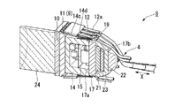
図2及び図3に示すように、撮像機構8は、観察対象物の像を撮像するために設けられており、イメージセンサ9と、保持部材14と、回路基板17と、カバー22とを備える。
As shown in FIGS. 2 and 3, the
イメージセンサ9は、複数の受光素子が整列配置されたセンサ面10及びセンサ面10の各受光素子から信号を読み出して出力する信号処理回路(不図示)が形成されたセンサ本体11と、信号処理回路に対して入出力を行うための入出力用リード12とを備える。
本実施形態では、センサ本体11は、センサ面10に直交する方向から見たときに矩形形状をなす板状となっている。また、センサ面10に直交する方向から見たときに、センサ本体11における対向する一組の辺のそれぞれからは、複数の上記入出力用リード12が延びている。また、センサ面10は、縦横比が4:3や16:9など所定の比となる矩形形状を有している。
本明細書では、センサ面10に直交する方向から見たときのセンサ本体11の輪郭形状が長方形をなしている場合を例に説明する。なお、センサ本体11の形状は、これに限られるものではない。
本実施形態では、イメージセンサ9の入出力用リード12は、センサ面10から保持部材14のセンサ接触面14a方向へ突出し、リード接触面14c方向へ曲げられてリード接触面14cへ向かって延びている。入出力用リード12は、センサ本体11からの突出方向を0度として、基端側へ90度以上曲げられている。各入出力用リード12は、後述する回路基板17に接する。また、入出力用リード12とセンサ本体11との間には、入出力用リード12とセンサ本体11との絶縁状態を保つための絶縁部材13が介在されている。
The
In the present embodiment, the
In this specification, the case where the contour shape of the
In this embodiment, the input /
図3及び図4に示すように、保持部材14は、イメージセンサ9においてセンサ面10が設けられた側とは反対側の面が接するセンサ接触面14aを有する絶縁性部材である。また、保持部材14には、イメージセンサ9の動作時にイメージセンサ9から発せられる熱の放熱経路となる導体パターン(不図示)が形成されている。
保持部材14の形状は、センサ接触面14aが底面となる枡状形状である。すなわち、保持部材14は、センサ接触面14aが設けられた側が封止され、センサ接触面14aが設けられた側と反対側が開口された容器形状をなしている。センサ接触面14aは、イメージセンサ9のセンサ面10と直交する方向から見たときにセンサ本体11の輪郭線よりも小さな長方形状に形成されている。また、保持部材14の外側輪郭線の形状は、略直方体形状となっている。
保持部材14の内部には、イメージセンサ9によって撮像された画像の後述する制御部52への出力を制御するための電子部品の一部と、各電子部品を絶縁する絶縁板15とが配置されている。保持部材14の内部において、動作時の発熱が小さな部品は保持部材14の底面側(先端構成部7における先端側)に配され、動作時の発熱が大きな部品は保持部材14の開口側(先端構成部7における基端側)に配されている。これにより、各電子部品の発熱によるイメージセンサ9への影響を低く抑えることができる。
保持部材14の開口の周囲は、後述する回路基板17と接する基板接触面14bとなっている。基板接触面14bには、イメージセンサ9のリードと後述する回路基板17の端子とを電気的に接続する中継配線部16が形成されている。
As shown in FIGS. 3 and 4, the holding
The shape of the holding
Inside the holding
The periphery of the opening of the holding
図3及び図5に示すように、中継配線部16は、保持部材14の外面に形成された薄板若しくは膜状の金属部材である。中継配線部16は、保持部材14の開口の四隅にそれぞれ配されている。各中継配線部16は、イメージセンサ9の入出力用リード12のうち、イメージセンサ9の四隅から延びる4つの隅部リード12aがそれぞれ接続されるようになっている。
中継配線部16と隅部リード12aとは、半田付けによって電気的かつ機械的に固定されている。
As shown in FIGS. 3 and 5, the
The
また、図3及び図4に示すように、保持部材14は、保持部材14の外面のうちセンサ接触面14aと交差するリード接触面14cを有している。リード接触面14cには、イメージセンサ9に設けられた複数の入出力用リード12のピッチに対応して配された複数の導体パターン14dが形成されている。
As shown in FIGS. 3 and 4, the holding
本実施形態では、導体パターン14dは、センサ接触面14aに直交する方向に長い矩形形状を有している。各導体パターン14dの長手方向の中間部において、導体パターン14dと入出力用リード12とが半田付けにより電気的且つ機械的に接続されている。なお、図3及び図4においては導体パターン14dと入出力用リード12とを接続する半田の図示が省略されている。
In the present embodiment, the
図3ないし図5に示すように、回路基板17は、イメージセンサ9のセンサ面10と平行に実装面17a、17bが向けられた板状部材である。回路基板17には、イメージセンサ9の動作を制御するためのカメラコントロールユニットの一部が配置されている。
図4に示すように、本実施形態では、回路基板17は、厚さ方向の両面が実装面(実装面17a、17b)とされており、回路基板17に実装される電子部品のうち、相対的に発熱量が多い電子部品は、保持部材14の開口に接する実装面17aとは反対側の実装面17b上に実装されている。
As shown in FIGS. 3 to 5, the
As shown in FIG. 4, in the present embodiment, the
図5に示すように、回路基板17の寸法は、実装面17a、17bと直交する方向(図4に符号Xで示す方向)から見たときの輪郭形状が略正方形状となっており、一辺の長さは、保持部材14をセンサ接触面14aと直交する方向から見たときの短辺の長さと略一致する長さとなっている。回路基板17の外面のうち、二つの実装面17a、17bと交差する面(以下、この面を「側面17c」と称する。)には、中継配線部16が接続される接点部18と、イメージセンサ9の入出力用リード12が接続される第二接点部19と、配線部4における後述する信号線4a及び撮像側電力線4bが接続される第三接点部20とが設けられている。
As shown in FIG. 5, the dimensions of the
接点部18は、実装面17a、17bと直交する方向(図4に符号Xで示す方向)から見たときに、回路基板17の側面17cのうち保持部材14の輪郭線の内側領域に位置する側面に設けられている。接点部18は、上記信号線4a若しくは撮像側電力線4bが入り込む溝を有する凹形状の金属薄膜によって構成されている。接点部18と中継配線部16とは、半田付け等によって電気的かつ機械的に接続されている。なお、接点部18は、必要に応じて、回路基板17の内部に設けられた図示しない内部配線を介して、回路基板17上に実装された各電子回路(例えば電子部品21)や、保持部材14内に配された電子部品等に電気的に接続されていてもよい。
The
第二接点部19は、イメージセンサ9の入出力用リード12の位置に対応した位置に設けられており、入出力用リード12が入り込む溝を有する凹形状の金属薄膜によって構成されている。第二接点部19は、入出力用リード12が直接半田付け等によって電気的かつ機械的に接続される。また、第二接点部19は、必要に応じて、回路基板17の内部に設けられた図示しない上記内部配線と接続される。なお、回路基板17内部に設けられた内部配線は、例えば金属の薄膜からなる導体パターンによって形成される。また、第二接点部19の少なくとも一部は、回路基板17の内部配線や回路基板17上に実装される電子部品(例えば電子部品21)との電気的な接続がされないダミーパッドであってもよい。
The
第三接点部20は、実装面17a、17bと直交する方向(図4に符号Xで示す方向)から見たときに、回路基板17の側面17cのうち保持部材14の上記輪郭線の内側領域に位置する側面に設けられ、2つの接点部18の間に配置されている。第三接点部20は、回路基板17の内部に設けられた図示しない内部配線を介して、回路基板17上に実装された各電子回路(例えば電子部品21)に電気的に接続されている。
When the
図3ないし図5に示すように、カバー22は、回路基板17の実装面17bに実装された電子部品21を外力から保護するための部材であり、かつ、これらの電子部品21から発せられた熱を放熱するための経路となる部材である。カバー22は、回路基板17の実装面17bの外周部分に沿うように回路基板17の実装面17bに固定されている。カバー22の材料は、たとえばセラミックスなど、外力を受けても変形しにくい材料であることが好ましい。
As shown in FIGS. 3 to 5, the
カバー22の形状は、実装面17a、17bに垂直な軸線回りに測った長さが、実装面17a、17bに近い側の端における長さよりも、実装面17a、17bから遠い側の端における長さの方が短い。すなわち、本実施形態では、カバー22は、先端構成部7の基端側に行くに従って漸次径が小さくなるように形成されている。カバー22の外面には、配線部4を構成する線の一部(例えば信号線4a及び撮像側電力線4b)が配置されている。配線部4は、カバー22の外面に沿って基端側へと延び、カバー22よりも基端側において束ねられている。
本実施形態では、カバー22は、実装面17bに接する面を底面とする角錐台状に形成されており、側面の一部が開口されている。
The shape of the
In the present embodiment, the
また、カバー22は、電子部品21に密着する熱伝導性の高い熱伝導シート23を有している。カバー22が回路基板17に固定されている状態で、熱伝導シート23は、電子部品21とカバー22の内面との双方に押し付けられている。カバー22及び熱伝導シート23は、絶縁性の材料によって形成されている。また、熱伝導シート23は、弾性を有していることが好ましい。
Further, the
図2に示すように、カバー22の外面には、回路基板17上に実装された電子部品21から発せられた熱を放熱するための金属線Cの先端が熱的に接続されている。金属線Cは、金属の編み線や撚り線によって形成されている。
なお、金属線Cとして、配線部4(信号線4a及び撮像側電力線4b)の一部を用いることもできる。例えば、信号線4aにノイズ低減用のシールド線がある場合、当該シールド線を用いてカバー22からの熱の拡散をさせることができる。
As shown in FIG. 2, the tip of a metal wire C for radiating heat generated from the
A part of the wiring part 4 (the
撮像機構8に接続される配線部4(信号線4a及び撮像側電力線4b)は、イメージセンサ9の入出力用リード12と直結する必要がない線が、第三接点部20に接続される。また、第三接点部20に配される信号線4a及び撮像側電力線4bは、これらの外径に基づいて優先順位がつけられて選択されている。すなわち、第三接点部20に配される信号線4a及び撮像側電力線4bは、最も外径が太い線から順に選択され第三接点部20に接続される。また、第三接点部20に接続される線に対応させて、回路基板17の内部配線の構成が決定される。第三接点部20に接続される線の外径は、芯線、被覆、及びシールド等の各構成要素の外径によって定まっている。たとえば、撮像機構8によって撮像された画像の信号を伝送するための信号線4aは、信号にノイズが混入するのを防止する目的で、芯線がシールドに覆われている場合があり、芯線と被覆のみからなる他の信号線4aと比較して外径が太くなる傾向がある。このため、信号線4aは、特に第三接点部20に接続されるのが好ましい。
The wiring unit 4 (
第三接点部20において、第三接点部20に接続される信号線4a及び撮像側電力線4bは、回路基板17の実装面17a、17bに垂直な方向から見たときにイメージセンサ9の輪郭線からはみ出さないようになっている。第二接点部19及び接点部18においても同様に、回路基板17の実装面17a、17bに垂直な方向から見たときにイメージセンサ9の輪郭線から信号線4a及び撮像側電力線4bがはみ出さないようになっている。
In the
撮像機構8に接続される信号線4a及び撮像側電力線4bは、カバー22の外面に沿って可撓管部3側へと延びており、一束にまとめられた状態で可撓管部3内に挿入されている。回路基板17の実装面17a、17bに垂直な方向から見たときに、撮像機構8に接続される信号線4a及び撮像側電力線4bは、イメージセンサ9の輪郭線の内側領域に収まっている。撮像機構8に接続される信号線4a及び撮像側電力線4bにおいて、回路基板17から上記一束にまとめられた部分までの間では、各線は接着剤等によって固定されており、外力によって各線が回路基板17から外れたり各線が断線したりしないようになっている。
The
図2に示すように、撮像光学系24は、イメージセンサ9のセンサ面10の中央を通りセンサ面10と直交するように光軸が位置決めされた光学系である。撮像光学系24の構成は特に限定されるものではなく、ズーム機構等を備えていてもよい。また、撮像光学系24には、光学特性を変更するための追加的な対物光学系25を組み合わせることもできる。例えば、本実施形態では、追加的な対物光学系25が光学アダプタ30に設けられている。
As shown in FIG. 2, the imaging
照明機構26は、光学アダプタ30内に設けられた光源27と、光源27から発せられる光の配光を制御するために光学アダプタ30に設けられた照明光学系28と、光源27に電力を供給する照明電力線29とを有する。光源27としては、たとえば発光ダイオード等を使用することができる。照明電力線29は、可撓管部3の内部を通じて操作部40の内部へと延び、後述する制御部52に接続されている。
The
図1に示すように、操作部40には、湾曲部5を湾曲させるために使用者が湾曲方向を入力するためのジョイスティック41が設けられている。本実施形態の内視鏡装置1では、ジョイスティック41は所定の中立位置に対して傾けられた方向が湾曲部5を湾曲させる方向として本体部50に入力される。本体では、ジョイスティック41からの入力に基づいて、湾曲部5を湾曲動作させる。
As shown in FIG. 1, the
本体部50は、表示部51と、制御部52と、電源部53とを備える。
表示部51は、撮像機構8によって撮像された画像を表示する装置であり、たとえば液晶表示パネル及び表示制御回路を有している。
The
The
制御部52は、上述の撮像機構8、照明機構26、及び表示部51の動作を制御するための各種電子部品を備える。
The
電源部53は、上述の撮像機構8、照明機構26、表示部51、及び制御部52を駆動させるための電力を供給するものであり、本実施形態では、バッテリーと、電力制御回路とを本体部50内に備えている。なお、バッテリー及び電力制御回路を本体部50内に備えることに代えて、若しくはバッテリー及び電力制御回路に加えて、商用電源を用いて内視鏡装置1を駆動させるための電源ユニットを本体内に備えていてもよい。
The
次に、本実施形態の撮像機構8及び内視鏡装置1の作用について説明する。
内視鏡装置1の挿入部2は、観察対象物の内部等に挿入されるものであり、小径であることが好ましい。このため、挿入部2の内部構造物を収容するための空間は限られている。たとえば、先端構成部7においては、限られた空間内に、撮像機構8と照明機構26とをともに収容する必要がある。また、先端構成部7は、撮像機構8と照明機構26とを外力から保護する目的で硬質となっている。ここで、先端構成部7の中心軸線方向の長さが長いと、狭い領域で曲率半径が小さく湾曲したような観察対象物になるほど、挿入部2の先端が曲がらずに突っかかるようになり、挿入部2の先端を案内するのが困難である。また、本実施形態では、撮像機構8の信号線4a及び撮像側電力線4bが互いに固定された部分も、柔軟性が乏しい部分であり、これらの硬質な構成部分により、挿入部2の先端部分には硬質部が生じる。
Next, the operation of the
The insertion part 2 of the endoscope apparatus 1 is inserted into the inside of the observation object, and preferably has a small diameter. For this reason, the space for accommodating the internal structure of the insertion part 2 is limited. For example, in the
図3及び図6に示すように、本実施形態では、撮像機構8の信号線4a及び撮像側電力線4bのうち外径が太い線(例えば図6に示す信号線4x,4y)が、優先的に第三接点部20に接続されており、先端構成部7の中心軸線方向から見たときにイメージセンサ9の輪郭線の内側に配置されている。
さらに、外径が太い線が、回路基板17の厚さ方向から見たときの回路基板17の中心に近い位置にあるので、当該太い線を他の線と一束にまとめるときに、撮像機構8の信号線4a及び撮像側電力線4bが互いに固定された部分の先端構成部7の中心軸線方向における長さを短くしても、当該太い線を曲げる量は少なくてよい。その結果、当該太い線を曲げることによる当該太い線への負荷が少ない状態で、硬質部の長さを短くすることができる。
As shown in FIGS. 3 and 6, in the present embodiment, of the
Furthermore, since the line having a thick outer diameter is located near the center of the
また、イメージセンサ9の受光素子数が多い場合には、イメージセンサの受光素子数が少ない場合と比較して、信号線4aを流れる信号が高周波となり、信号に対するノイズの影響が大きくなりやすい。このため、このようなイメージセンサ9を使用する場合には、信号線4aにシールドを設けたり、各信号線4aとグランド線とをツイストペア構成としたりするなど、信号線4aの外径が太くなりやすい。また、イメージセンサ9の受光素子数が多い場合には、イメージセンサ9が大型となる傾向がある。この場合、イメージセンサ9のセンサ面10に垂直な方向から見たときにイメージセンサ9の輪郭線から信号線4aがはみ出すと、先端構成部7が大径となってしまうおそれがある。
In addition, when the number of light receiving elements of the
これに対して、図6に示すように、本実施形態の撮像機構8は、イメージセンサ9のセンサ面10と直交する方向、すなわち先端構成部7の中心軸線方向から見たときに、信号線4a及び撮像側電力線4bは、イメージセンサ9の輪郭線の内側に収まっている。このため、イメージセンサ9のセンサ面10に垂直な方向から見たときの撮像機構8の寸法はイメージセンサ9の寸法によって規定されることとなる。このため、撮像機構8に接続される信号線4a及び撮像側電力線4bがイメージセンサ9の輪郭線からはみ出すことによる先端構成部7の大径化が防止される。
On the other hand, as shown in FIG. 6, the
また、撮像機構8の動作時には、イメージセンサ9その他の電子部品から発せられる熱により、イメージセンサ9に対する暗電流に起因する熱ノイズが生じる場合がある。本実施形態では、イメージセンサ9から発せられた熱は、図4に示す保持部材14、回路基板17、熱伝導シート23、及びカバー22を通じて金属線C(図2参照)へと拡散する。これにより、イメージセンサ9の温度が上昇することによって画像に生じるノイズを低減させることができる。特に、イメージセンサ9上に構成される受光素子数が多くなったり、信号処理回路の動作周波数が高くなったりすると、イメージセンサ9の発熱量は大きくなる。
本実施形態では、挿入部2の先端から基端へ向かって直線的に放熱経路が設けられていることにより、挿入部2の先端に配されたイメージセンサ9その他の電子部品の熱が挿入部2の先端側にこもるのを低減することができる。これにより、イメージセンサ9によって撮像された画像の画質の低下を抑制することができる。
Further, when the
In the present embodiment, since the heat radiation path is provided linearly from the distal end of the insertion portion 2 to the proximal end, the heat of the
以上説明したように、本実施形態の撮像機構8及び内視鏡装置1によれば、挿入部2の硬質部の長さが長くなるのを抑えつつ、大型のイメージセンサ9を搭載することができる。その結果、高画質のイメージセンサ9を搭載しても挿入部2の大型化を抑えることができる。
As described above, according to the
また、従来と同等のイメージセンサを搭載する場合には、硬質部の長さを短くすることができる。 In addition, when an image sensor equivalent to the conventional one is mounted, the length of the hard portion can be shortened.
また、イメージセンサ9が発する熱を好適に挿入部2の基端側へと移動させる経路を有しているので、イメージセンサ9に対する熱ノイズの影響を少なく抑え、画質の高い画像を撮像することができる。
In addition, since it has a path for moving the heat generated by the
以上、本発明の実施形態について図面を参照して詳述したが、具体的な構成はこの実施形態に限られるものではなく、本発明の要旨を逸脱しない範囲の設計変更等も含まれる。
例えば、熱伝導シート23に代えて、熱伝導性の高いグリスが設けられていてもよい。
また、保持部材のセンサ接触面は、イメージセンサのセンサ面と直交する方向から見たときにセンサ本体の輪郭線と一致する長方形状(略一致する長方形状を含む)とされていてもよい。
また、中継配線部は、基板接触面以外の面に設けられていてもよい。また、中継配線部は、保持部材のリード接触面に形成された導体パターンと接続されていてもよい。
また、中継配線部は、回路基板の側面に形成されていてもよい。
さらに、保持部材と回路基板との両方に中継配線部が形成されていてもよい。この場合、保持部材に形成された中継配線部と回路基板に形成された中継配線部と互いに電気的に導通した状態で設けられている。
As mentioned above, although embodiment of this invention was explained in full detail with reference to drawings, the concrete structure is not restricted to this embodiment, The design change etc. of the range which does not deviate from the summary of this invention are included.
For example, instead of the heat
Further, the sensor contact surface of the holding member may have a rectangular shape (including a substantially matching rectangular shape) that matches the contour of the sensor body when viewed from a direction orthogonal to the sensor surface of the image sensor.
In addition, the relay wiring portion may be provided on a surface other than the substrate contact surface. The relay wiring portion may be connected to a conductor pattern formed on the lead contact surface of the holding member.
Moreover, the relay wiring part may be formed on the side surface of the circuit board.
Furthermore, the relay wiring part may be formed on both the holding member and the circuit board. In this case, the relay wiring portion formed on the holding member and the relay wiring portion formed on the circuit board are provided in an electrically conductive state.
なお、本発明の実施形態に対する設計変更等は上記例示には限定されない。 In addition, the design change etc. with respect to embodiment of this invention are not limited to the said illustration.
1 内視鏡装置
2 挿入部
3 可撓管部
4 配線部
4a 信号線
4b 撮像側電力線
4x 信号線
5 湾曲部
6 節輪等
7 先端構成部
8 撮像機構
9 イメージセンサ
W アングルワイヤ
10 センサ面
11 センサ本体
12 入出力用リード
12a 隅部リード(入出力用リード)
13 絶縁部材
14 保持部材
14a センサ接触面
14b 基板接触面
14c リード接触面
14d 導体パターン
15 絶縁板
16 中継配線部
17 回路基板
17a 実装面
17b 実装面
17c 側面
18 接点部
19 第二接点部
20 第三接点部
21 電子部品
22 カバー
23 熱伝導シート
24 撮像光学系
25 対物光学系
26 照明機構
27 光源
28 照明光学系
29 照明電力線
30 光学アダプタ
40 操作部
41 ジョイスティック
50 本体部
51 表示部
52 制御部
53 電源部
DESCRIPTION OF SYMBOLS 1 Endoscope apparatus 2 Insertion part 3
13 Insulating
Claims (10)
前記イメージセンサにおいて前記センサ面が設けられた側とは反対側の面に接するセンサ接触面を有する保持部材と、
前記保持部材における前記センサ接触面と反対側の外面に固定され、前記センサ面と平行な実装面を有し、前記実装面に垂直な方向から見たときに輪郭線の少なくとも一部が前記保持部材の輪郭線の内側に位置する回路基板と、
前記回路基板において前記実装面と交差して形成された側面上であって前記回路基板の輪郭線が前記保持部材の輪郭線の内側に位置している領域内に配された接点部と、
を備え、
前記保持部材と前記回路基板との少なくともいずれかは、前記接点部が電気的に接続されているとともに前記入出力用リードの少なくとも一つが電気的に接続された中継配線部を有し、
前記接点部には、前記イメージセンサに対して電力若しくは電気信号を伝送するための第一配線が接続され、
前記側面のうち前記接点部が配された面とは異なる面上には、前記入出力用リードの少なくとも他の一つが接続され且つ前記イメージセンサに対して電力若しくは電気信号を伝送するための第二配線が接続される第二接点部が設けられており、
前記第一配線のうちの少なくとも一つは前記第二配線よりも外径が太いことを特徴とする撮像機構。 An image sensor having a sensor surface on which a plurality of light receiving elements are arranged and a plurality of input / output leads;
A holding member having a sensor contact surface in contact with a surface opposite to the side on which the sensor surface is provided in the image sensor;
The holding member is fixed to an outer surface opposite to the sensor contact surface, has a mounting surface parallel to the sensor surface, and at least a part of a contour line when viewed from a direction perpendicular to the mounting surface holds the holding A circuit board located inside the contour of the member;
A contact portion disposed on a side surface of the circuit board that intersects with the mounting surface, the contour line of the circuit board being located inside the contour line of the holding member;
With
At least one of the holding member and the circuit board has a relay wiring portion in which the contact portion is electrically connected and at least one of the input / output leads is electrically connected ,
A first wiring for transmitting electric power or an electric signal to the image sensor is connected to the contact portion,
At least one other of the input / output leads is connected to a surface different from the surface on which the contact portion is disposed among the side surfaces, and a power or electric signal is transmitted to the image sensor. A second contact point to which two wires are connected is provided,
At least one of the first wirings has an outer diameter larger than that of the second wiring .
前記イメージセンサにおいて前記センサ面が設けられた側とは反対側の面に接するセンサ接触面を有する保持部材と、
前記保持部材における前記センサ接触面と反対側の外面に固定され、前記センサ面と平行な実装面を有し、前記実装面に垂直な方向から見たときに輪郭線の少なくとも一部が前記保持部材の輪郭線の内側に位置する回路基板と、
前記回路基板において前記実装面と交差して形成された側面上であって前記回路基板の輪郭線が前記保持部材の輪郭線の内側に位置している領域内に配された接点部と、
を備え、
前記保持部材と前記回路基板との少なくともいずれかは、前記接点部が電気的に接続されているとともに前記入出力用リードの少なくとも一つが電気的に接続された中継配線部を有し、
前記側面のうち前記接点部が配された面とは異なる面上には、前記入出力用リードの少なくとも他の一つが接続され且つ前記イメージセンサに対して電力若しくは電気信号を伝送するための第二配線が接続される第二接点部が設けられており、
前記領域内には、前記接点部と異なる第三接点部が配され、
前記第三接点部は、前記回路基板に設けられた導体パターンと接続され、前記回路基板上に実装された電子部品と電気的に接続され、
前記第三接点部には、前記電子部品と前記イメージセンサとの少なくともいずれかに対して電力若しくは電気信号を伝送するための第三配線が電気的且つ機械的に接続されることを特徴とする撮像機構。 An image sensor having a sensor surface on which a plurality of light receiving elements are arranged and a plurality of input / output leads;
A holding member having a sensor contact surface in contact with a surface opposite to the side on which the sensor surface is provided in the image sensor;
The holding member is fixed to an outer surface opposite to the sensor contact surface, has a mounting surface parallel to the sensor surface, and at least a part of a contour line when viewed from a direction perpendicular to the mounting surface holds the holding A circuit board located inside the contour of the member;
A contact portion disposed on a side surface of the circuit board that intersects with the mounting surface, the contour line of the circuit board being located inside the contour line of the holding member;
With
At least one of the holding member and the circuit board has a relay wiring portion in which the contact portion is electrically connected and at least one of the input / output leads is electrically connected,
At least one other of the input / output leads is connected to a surface different from the surface on which the contact portion is disposed among the side surfaces, and a power or electric signal is transmitted to the image sensor. A second contact point to which two wires are connected is provided,
In the region, a third contact portion different from the contact portion is arranged,
The third contact portion is connected to a conductor pattern provided on the circuit board, and is electrically connected to an electronic component mounted on the circuit board,
A third wiring for transmitting electric power or an electric signal to at least one of the electronic component and the image sensor is electrically and mechanically connected to the third contact portion. that an imaging mechanism.
前記第三接点部に接続された前記第三配線のうちの少なくとも一つは前記第二配線よりも外径が太いことを特徴とする請求項2に記載の撮像機構。 One or more third contact portions are provided,
The imaging mechanism according to claim 2 , wherein at least one of the third wirings connected to the third contact portion has a larger outer diameter than the second wiring.
前記イメージセンサにおいて前記センサ面が設けられた側とは反対側の面に接するセンサ接触面を有する保持部材と、
前記保持部材における前記センサ接触面と反対側の外面に固定され、前記センサ面と平行な実装面を有し、前記実装面に垂直な方向から見たときに輪郭線の少なくとも一部が前記保持部材の輪郭線の内側に位置する回路基板と、
前記回路基板において前記実装面と交差して形成された側面上であって前記回路基板の輪郭線が前記保持部材の輪郭線の内側に位置している領域内に配された接点部と、
を備え、
前記保持部材と前記回路基板との少なくともいずれかは、前記接点部が電気的に接続されているとともに前記入出力用リードの少なくとも一つが電気的に接続された中継配線部を有し、
前記回路基板の実装面には、前記実装面と平行な外面を有する電子部品が実装され、
前記回路基板には、前記電子部品を覆い熱伝導性を有する絶縁性のカバーが固定され、
前記電子部品の前記外面と前記カバーとの間には、熱伝導性を有する絶縁性の熱伝導シートが介在されていることを特徴とする撮像機構。 An image sensor having a sensor surface on which a plurality of light receiving elements are arranged and a plurality of input / output leads;
A holding member having a sensor contact surface in contact with a surface opposite to the side on which the sensor surface is provided in the image sensor;
The holding member is fixed to an outer surface opposite to the sensor contact surface, has a mounting surface parallel to the sensor surface, and at least a part of a contour line when viewed from a direction perpendicular to the mounting surface holds the holding A circuit board located inside the contour of the member;
A contact portion disposed on a side surface of the circuit board that intersects with the mounting surface, the contour line of the circuit board being located inside the contour line of the holding member;
With
At least one of the holding member and the circuit board has a relay wiring portion in which the contact portion is electrically connected and at least one of the input / output leads is electrically connected,
An electronic component having an outer surface parallel to the mounting surface is mounted on the mounting surface of the circuit board,
An insulating cover having heat conductivity covering the electronic component is fixed to the circuit board,
The electronic component between said exterior surface and said cover, characterized in that the insulating thermally conductive sheet having a thermal conductivity is interposed an imaging mechanism.
前記接点部には、イメージセンサに対して電力若しくは電気信号を伝送するための第一配線が接続され、
前記第三接点部は、前記複数の接点部の間に設けられ、
前記第三接点部に接続された前記第三配線のうちの少なくとも一つは、前記第一配線よりも外径が太いことを特徴とする請求項2に記載の撮像機構。 A plurality of the contact portions are provided,
A first wiring for transmitting power or an electrical signal to the image sensor is connected to the contact portion,
The third contact portion is provided between the plurality of contact portions,
The imaging mechanism according to claim 2 , wherein at least one of the third wirings connected to the third contact portion has a larger outer diameter than the first wiring.
前記イメージセンサにおいて前記センサ面が設けられた側とは反対側の面に接するセンサ接触面を有する保持部材と、
前記保持部材における前記センサ接触面と反対側の外面に固定され、前記センサ面と平行な実装面を有し、前記実装面に垂直な方向から見たときに輪郭線の少なくとも一部が前記保持部材の輪郭線の内側に位置する回路基板と、
前記回路基板において前記実装面と交差して形成された側面上であって前記回路基板の輪郭線が前記保持部材の輪郭線の内側に位置している領域内に配された接点部と、
を備え、
前記保持部材と前記回路基板との少なくともいずれかは、前記接点部が電気的に接続されているとともに前記入出力用リードの少なくとも一つが電気的に接続された中継配線部を有し、
前記保持部材は、当該保持部材の外面のうち前記センサ接触面と交差するリード接触面を有し、
前記入出力用リードは、前記センサ面から前記センサ接触面方向へ突出し前記リード接触面方向へ曲げられて前記リード接触面へ向かって延びており、
前記リード接触面上には、前記入出力用リードのピッチに対応して配され前記入出力用リードが電気的且つ機械的に接続される導体パターンが形成されていることを特徴とする撮像機構。 An image sensor having a sensor surface on which a plurality of light receiving elements are arranged and a plurality of input / output leads;
A holding member having a sensor contact surface in contact with a surface opposite to the side on which the sensor surface is provided in the image sensor;
The holding member is fixed to an outer surface opposite to the sensor contact surface, has a mounting surface parallel to the sensor surface, and at least a part of a contour line when viewed from a direction perpendicular to the mounting surface holds the holding A circuit board located inside the contour of the member;
A contact portion disposed on a side surface of the circuit board that intersects with the mounting surface, the contour line of the circuit board being located inside the contour line of the holding member;
With
At least one of the holding member and the circuit board has a relay wiring portion in which the contact portion is electrically connected and at least one of the input / output leads is electrically connected,
The holding member has a lead contact surface that intersects the sensor contact surface of the outer surface of the holding member,
The input / output lead protrudes from the sensor surface toward the sensor contact surface, is bent toward the lead contact surface, and extends toward the lead contact surface.
On the lead contact surface, shooting you, characterized in that the conductor pattern in which the input and output leads are disposed corresponding to the pitch of the input and output leads are electrically and mechanically connected are formed Image mechanism.
前記挿入部の先端に配され観察対象物を撮像するための請求項1から請求項8のいずれか一項に記載の撮像機構と、
前記挿入部の基端に設けられた操作部と、
を備えることを特徴とする内視鏡装置。 A long insertion portion having a distal end and a proximal end;
The imaging mechanism according to any one of claims 1 to 8 , which is arranged at a distal end of the insertion portion and images an observation object;
An operation portion provided at a proximal end of the insertion portion;
An endoscope apparatus comprising:
前記挿入部の先端に配され観察対象物を撮像するための請求項4または請求項5に記載の撮像機構と、
前記挿入部の基端に設けられた本体部と、
を備え、
前記挿入部の内部には、先端が前記カバーに熱的に接続された金属線が設けられていることを特徴とする内視鏡装置。 A long insertion portion having a distal end and a proximal end;
The imaging mechanism according to claim 4 or 5 , wherein the imaging mechanism is arranged at the distal end of the insertion portion and images an observation object.
A main body provided at the proximal end of the insertion portion;
With
An endoscope apparatus, wherein a metal wire whose tip is thermally connected to the cover is provided inside the insertion portion.
Priority Applications (4)
| Application Number | Priority Date | Filing Date | Title |
|---|---|---|---|
| JP2011289349A JP5926955B2 (en) | 2011-12-28 | 2011-12-28 | Imaging mechanism and endoscope apparatus |
| EP12008318.3A EP2609850B1 (en) | 2011-12-28 | 2012-12-13 | Imaging mechanism and endoscope apparatus |
| US13/716,494 US9325881B2 (en) | 2011-12-28 | 2012-12-17 | Imaging mechanism and endoscope apparatus |
| CN201210563319.6A CN103185960B (en) | 2011-12-28 | 2012-12-21 | Image mechanism and endoscope apparatus |
Applications Claiming Priority (1)
| Application Number | Priority Date | Filing Date | Title |
|---|---|---|---|
| JP2011289349A JP5926955B2 (en) | 2011-12-28 | 2011-12-28 | Imaging mechanism and endoscope apparatus |
Publications (3)
| Publication Number | Publication Date |
|---|---|
| JP2013135823A JP2013135823A (en) | 2013-07-11 |
| JP2013135823A5 JP2013135823A5 (en) | 2015-01-22 |
| JP5926955B2 true JP5926955B2 (en) | 2016-05-25 |
Family
ID=47602729
Family Applications (1)
| Application Number | Title | Priority Date | Filing Date |
|---|---|---|---|
| JP2011289349A Expired - Fee Related JP5926955B2 (en) | 2011-12-28 | 2011-12-28 | Imaging mechanism and endoscope apparatus |
Country Status (4)
| Country | Link |
|---|---|
| US (1) | US9325881B2 (en) |
| EP (1) | EP2609850B1 (en) |
| JP (1) | JP5926955B2 (en) |
| CN (1) | CN103185960B (en) |
Cited By (1)
| Publication number | Priority date | Publication date | Assignee | Title |
|---|---|---|---|---|
| JP6998939B2 (en) | 2017-03-31 | 2022-01-18 | 東洋鋼鈑株式会社 | Hydroponics unit and hydroponics system including this hydroponics unit |
Families Citing this family (24)
| Publication number | Priority date | Publication date | Assignee | Title |
|---|---|---|---|---|
| WO2012033936A2 (en) | 2010-09-08 | 2012-03-15 | Tyco Healthcare Group Lp | Catheter with imaging assembly |
| CA2878514A1 (en) | 2012-07-26 | 2014-01-30 | Olive Medical Corporation | Ycbcr pulsed illumination scheme in a light deficient environment |
| CA2878511A1 (en) | 2012-07-26 | 2014-01-30 | Olive Medical Corporation | Continuous video in a light deficient environment |
| US9198835B2 (en) | 2012-09-07 | 2015-12-01 | Covidien Lp | Catheter with imaging assembly with placement aid and related methods therefor |
| US9517184B2 (en) | 2012-09-07 | 2016-12-13 | Covidien Lp | Feeding tube with insufflation device and related methods therefor |
| USD716841S1 (en) | 2012-09-07 | 2014-11-04 | Covidien Lp | Display screen with annotate file icon |
| USD735343S1 (en) | 2012-09-07 | 2015-07-28 | Covidien Lp | Console |
| USD717340S1 (en) | 2012-09-07 | 2014-11-11 | Covidien Lp | Display screen with enteral feeding icon |
| WO2014144947A1 (en) | 2013-03-15 | 2014-09-18 | Olive Medical Corporation | Super resolution and color motion artifact correction in a pulsed color imaging system |
| US10251530B2 (en) | 2013-03-15 | 2019-04-09 | DePuy Synthes Products, Inc. | Scope sensing in a light controlled environment |
| JP5767414B2 (en) * | 2013-08-05 | 2015-08-19 | オリンパス株式会社 | Endoscope imaging unit |
| WO2015045467A1 (en) * | 2013-09-25 | 2015-04-02 | オリンパスメディカルシステムズ株式会社 | Electrical unit and endoscope having same mounted thereto |
| CN105101864B (en) * | 2013-09-26 | 2017-04-26 | 奥林巴斯株式会社 | Endoscope device |
| CN104902802B (en) * | 2013-10-04 | 2017-03-15 | 奥林巴斯株式会社 | Endoscopic image pickup unit |
| JP5806343B2 (en) * | 2014-01-16 | 2015-11-10 | ソニー・オリンパスメディカルソリューションズ株式会社 | Photoelectric composite module, camera head, and endoscope apparatus |
| JP6344935B2 (en) * | 2014-03-13 | 2018-06-20 | Hoya株式会社 | Semiconductor device and endoscope |
| CN106102559A (en) * | 2014-03-21 | 2016-11-09 | 德普伊新特斯产品公司 | Bayonet connector for imaging sensor |
| WO2016092986A1 (en) * | 2014-12-08 | 2016-06-16 | オリンパス株式会社 | Imaging unit, imaging module, and endoscope system |
| JP6539548B2 (en) * | 2015-08-31 | 2019-07-03 | 富士フイルム株式会社 | Endoscope imaging apparatus and endoscope |
| WO2017141397A1 (en) * | 2016-02-18 | 2017-08-24 | オリンパス株式会社 | Imaging device and endoscope |
| JP6307697B1 (en) * | 2016-05-10 | 2018-04-11 | オリンパス株式会社 | Electronic circuit unit, imaging unit, imaging module, and endoscope |
| JP2019076358A (en) * | 2017-10-24 | 2019-05-23 | オリンパス株式会社 | Image pickup module, endoscope, and method of manufacturing image pickup module |
| JP7132007B2 (en) * | 2018-07-18 | 2022-09-06 | i-PRO株式会社 | Imaging unit for endoscope and endoscope |
| CN113660815B (en) * | 2021-10-20 | 2022-02-08 | 上海宇度医学科技股份有限公司 | Support wiring assembly, wiring method and endoscope head |
Family Cites Families (14)
| Publication number | Priority date | Publication date | Assignee | Title |
|---|---|---|---|---|
| US4491865A (en) * | 1982-09-29 | 1985-01-01 | Welch Allyn, Inc. | Image sensor assembly |
| US6142930A (en) * | 1997-01-13 | 2000-11-07 | Asahi Kogaku Kogyo Kabushiki Kaisha | Electronic endoscope having compact construction |
| US5929901A (en) * | 1997-10-06 | 1999-07-27 | Adair; Edwin L. | Reduced area imaging devices incorporated within surgical instruments |
| JPH11326787A (en) * | 1998-05-15 | 1999-11-26 | Olympus Optical Co Ltd | Image pickup device |
| JP2000199863A (en) * | 1999-01-07 | 2000-07-18 | Sony Corp | Solid-state image pickup device |
| DE19924189C2 (en) | 1999-05-27 | 2001-04-26 | Storz Karl Gmbh & Co Kg | Image sensor module and method for assembling such an image sensor module |
| JP4153733B2 (en) * | 2002-06-24 | 2008-09-24 | オリンパス株式会社 | Endoscope |
| EP1406311B1 (en) * | 2002-10-02 | 2008-07-23 | STMicroelectronics Limited | Methods and apparatus for sensor alignment |
| JP4575698B2 (en) * | 2004-04-08 | 2010-11-04 | Hoya株式会社 | The tip of the electronic endoscope |
| JP4512452B2 (en) | 2004-08-31 | 2010-07-28 | Hoya株式会社 | The tip of the electronic endoscope |
| US8289381B2 (en) * | 2005-01-05 | 2012-10-16 | Avantis Medical Systems, Inc. | Endoscope with an imaging catheter assembly and method of configuring an endoscope |
| JP2008212363A (en) * | 2007-03-02 | 2008-09-18 | Hoya Corp | Endoscope |
| DE102007034704A1 (en) * | 2007-07-18 | 2009-01-22 | Karl Storz Gmbh & Co. Kg | The image pick |
| CN102572229A (en) * | 2010-12-29 | 2012-07-11 | 鸿富锦精密工业(深圳)有限公司 | Camera module |
-
2011
- 2011-12-28 JP JP2011289349A patent/JP5926955B2/en not_active Expired - Fee Related
-
2012
- 2012-12-13 EP EP12008318.3A patent/EP2609850B1/en not_active Not-in-force
- 2012-12-17 US US13/716,494 patent/US9325881B2/en active Active
- 2012-12-21 CN CN201210563319.6A patent/CN103185960B/en active Active
Cited By (1)
| Publication number | Priority date | Publication date | Assignee | Title |
|---|---|---|---|---|
| JP6998939B2 (en) | 2017-03-31 | 2022-01-18 | 東洋鋼鈑株式会社 | Hydroponics unit and hydroponics system including this hydroponics unit |
Also Published As
| Publication number | Publication date |
|---|---|
| US9325881B2 (en) | 2016-04-26 |
| EP2609850A1 (en) | 2013-07-03 |
| EP2609850B1 (en) | 2017-02-01 |
| US20130169777A1 (en) | 2013-07-04 |
| JP2013135823A (en) | 2013-07-11 |
| CN103185960B (en) | 2017-03-29 |
| CN103185960A (en) | 2013-07-03 |
Similar Documents
| Publication | Publication Date | Title |
|---|---|---|
| JP5926955B2 (en) | Imaging mechanism and endoscope apparatus | |
| CN107149460B (en) | Endoscope with a detachable handle | |
| CN106886089B (en) | Endoscope with a detachable handle | |
| JP6625630B2 (en) | Imaging device, endoscope system, and method of manufacturing imaging device | |
| EP3050491B1 (en) | Endoscope device | |
| JP2013135823A5 (en) | ||
| WO2017199406A1 (en) | Cable connection board, image pickup device, endoscope, and method for manufacturing image pickup device | |
| JP6643396B2 (en) | Three-dimensional wiring board, imaging unit | |
| CN107802227B (en) | Endoscope and method for operating the same | |
| US10925464B2 (en) | Imaging unit and endoscope | |
| JP2017046832A (en) | Endoscope imaging apparatus and endoscope | |
| WO2019176601A1 (en) | Imaging unit and oblique endoscope | |
| JP6630639B2 (en) | Endoscope | |
| US10757309B2 (en) | Endoscope imaging module with signal cable and flexible linear structure | |
| US10842365B2 (en) | Image pickup apparatus and endoscope | |
| JP6727964B2 (en) | Endoscope | |
| JP7163333B2 (en) | Endoscope | |
| US10888217B2 (en) | Imaging module applicable to head-swing endoscope | |
| US20220079428A1 (en) | Image pickup module and endoscope | |
| WO2016185554A1 (en) | Image pickup unit and endoscope | |
| WO2017115441A1 (en) | Mounting structure, image pickup device, and endoscope |
Legal Events
| Date | Code | Title | Description |
|---|---|---|---|
| A521 | Request for written amendment filed |
Free format text: JAPANESE INTERMEDIATE CODE: A523 Effective date: 20141203 |
|
| A621 | Written request for application examination |
Free format text: JAPANESE INTERMEDIATE CODE: A621 Effective date: 20141203 |
|
| A977 | Report on retrieval |
Free format text: JAPANESE INTERMEDIATE CODE: A971007 Effective date: 20150929 |
|
| A131 | Notification of reasons for refusal |
Free format text: JAPANESE INTERMEDIATE CODE: A131 Effective date: 20151104 |
|
| A521 | Request for written amendment filed |
Free format text: JAPANESE INTERMEDIATE CODE: A523 Effective date: 20151119 |
|
| A521 | Request for written amendment filed |
Free format text: JAPANESE INTERMEDIATE CODE: A821 Effective date: 20151120 |
|
| TRDD | Decision of grant or rejection written | ||
| A01 | Written decision to grant a patent or to grant a registration (utility model) |
Free format text: JAPANESE INTERMEDIATE CODE: A01 Effective date: 20160329 |
|
| A61 | First payment of annual fees (during grant procedure) |
Free format text: JAPANESE INTERMEDIATE CODE: A61 Effective date: 20160425 |
|
| R151 | Written notification of patent or utility model registration |
Ref document number: 5926955 Country of ref document: JP Free format text: JAPANESE INTERMEDIATE CODE: R151 |
|
| R250 | Receipt of annual fees |
Free format text: JAPANESE INTERMEDIATE CODE: R250 |
|
| R250 | Receipt of annual fees |
Free format text: JAPANESE INTERMEDIATE CODE: R250 |
|
| R250 | Receipt of annual fees |
Free format text: JAPANESE INTERMEDIATE CODE: R250 |
|
| R250 | Receipt of annual fees |
Free format text: JAPANESE INTERMEDIATE CODE: R250 |
|
| S111 | Request for change of ownership or part of ownership |
Free format text: JAPANESE INTERMEDIATE CODE: R313111 |
|
| R371 | Transfer withdrawn |
Free format text: JAPANESE INTERMEDIATE CODE: R371 |
|
| S111 | Request for change of ownership or part of ownership |
Free format text: JAPANESE INTERMEDIATE CODE: R313111 |
|
| R371 | Transfer withdrawn |
Free format text: JAPANESE INTERMEDIATE CODE: R371 |
|
| LAPS | Cancellation because of no payment of annual fees |