JP2017502606A - Pseudo Yagi type antenna - Google Patents
Pseudo Yagi type antenna Download PDFInfo
- Publication number
- JP2017502606A JP2017502606A JP2016544657A JP2016544657A JP2017502606A JP 2017502606 A JP2017502606 A JP 2017502606A JP 2016544657 A JP2016544657 A JP 2016544657A JP 2016544657 A JP2016544657 A JP 2016544657A JP 2017502606 A JP2017502606 A JP 2017502606A
- Authority
- JP
- Japan
- Prior art keywords
- antenna
- ground plane
- balun
- coupled
- signal
- Prior art date
- Legal status (The legal status is an assumption and is not a legal conclusion. Google has not performed a legal analysis and makes no representation as to the accuracy of the status listed.)
- Pending
Links
Images


Classifications
-
- H—ELECTRICITY
- H01—ELECTRIC ELEMENTS
- H01Q—ANTENNAS, i.e. RADIO AERIALS
- H01Q19/00—Combinations of primary active antenna elements and units with secondary devices, e.g. with quasi-optical devices, for giving the antenna a desired directional characteristic
- H01Q19/28—Combinations of primary active antenna elements and units with secondary devices, e.g. with quasi-optical devices, for giving the antenna a desired directional characteristic using a secondary device in the form of two or more substantially straight conductive elements
- H01Q19/30—Combinations of primary active antenna elements and units with secondary devices, e.g. with quasi-optical devices, for giving the antenna a desired directional characteristic using a secondary device in the form of two or more substantially straight conductive elements the primary active element being centre-fed and substantially straight, e.g. Yagi antenna
-
- H—ELECTRICITY
- H01—ELECTRIC ELEMENTS
- H01Q—ANTENNAS, i.e. RADIO AERIALS
- H01Q1/00—Details of, or arrangements associated with, antennas
- H01Q1/48—Earthing means; Earth screens; Counterpoises
-
- H—ELECTRICITY
- H01—ELECTRIC ELEMENTS
- H01Q—ANTENNAS, i.e. RADIO AERIALS
- H01Q1/00—Details of, or arrangements associated with, antennas
- H01Q1/50—Structural association of antennas with earthing switches, lead-in devices or lightning protectors
-
- H—ELECTRICITY
- H01—ELECTRIC ELEMENTS
- H01Q—ANTENNAS, i.e. RADIO AERIALS
- H01Q21/00—Antenna arrays or systems
- H01Q21/0006—Particular feeding systems
-
- H—ELECTRICITY
- H01—ELECTRIC ELEMENTS
- H01Q—ANTENNAS, i.e. RADIO AERIALS
- H01Q21/00—Antenna arrays or systems
- H01Q21/06—Arrays of individually energised antenna units similarly polarised and spaced apart
- H01Q21/061—Two dimensional planar arrays
- H01Q21/062—Two dimensional planar arrays using dipole aerials
-
- H—ELECTRICITY
- H01—ELECTRIC ELEMENTS
- H01Q—ANTENNAS, i.e. RADIO AERIALS
- H01Q9/00—Electrically-short antennas having dimensions not more than twice the operating wavelength and consisting of conductive active radiating elements
- H01Q9/04—Resonant antennas
- H01Q9/16—Resonant antennas with feed intermediate between the extremities of the antenna, e.g. centre-fed dipole
- H01Q9/20—Two collinear substantially straight active elements; Substantially straight single active elements
Landscapes
- Variable-Direction Aerials And Aerial Arrays (AREA)
- Aerials With Secondary Devices (AREA)
- Waveguide Aerials (AREA)
- Details Of Aerials (AREA)
- Support Of Aerials (AREA)
Abstract
装置が、第1の接地面と、第2の接地面と、アンテナと、アンテナに結合されるバランとを含む。バランは第1の接地面と第2の接地面との間に配置される。The apparatus includes a first ground plane, a second ground plane, an antenna, and a balun coupled to the antenna. The balun is disposed between the first ground plane and the second ground plane.
Description
関連出願の相互参照
本出願は、それらの内容が全体を参照することにより本明細書に明確に組み込まれている、2014年1月8日に出願された共同所有の米国仮特許出願第61/925,011号、および2014年12月5日に出願された米国非仮特許出願第14/561,680号の優先権を主張する。
CROSS REFERENCE TO RELATED APPLICATIONS This application is a co-owned US Provisional Patent Application No. 61 / filed January 8, 2014, the contents of which are expressly incorporated herein by reference in their entirety. 925,011 and US non-provisional patent application No. 14 / 561,680 filed Dec. 5, 2014.
本開示は包括的にはアンテナに関する。 The present disclosure relates generally to antennas.
技術が進歩した結果、コンピューティングデバイスがより小型に、そしてより強力になった。たとえば、小型、軽量であり、ユーザによる持ち運びが容易な、ポータブルワイヤレス電話、携帯情報端末(PDA)、ページングデバイスなどのワイヤレスコンピューティングデバイスを含む種々のポータブルパーソナルコンピューティングデバイスが現存している。より具体的には、セルラー電話、インターネットプロトコル(IP)電話などのポータブルワイヤレス電話は、ワイヤレスネットワークを介して音声およびデータパケットを通信することができる。さらに、多くのそのようなワイヤレス電話は、その内部に組み込まれた他のタイプのデバイスを含む。たとえば、ワイヤレス電話は、デジタルスチールカメラ、デジタルビデオカメラ、デジタルレコーダ、およびオーディオファイルプレーヤを含むこともできる。また、そのようなワイヤレス電話は、インターネットにアクセスするために使用することができるウェブブラウザアプリケーションなどのソフトウェアアプリケーションを含む実行可能命令を処理することができる。したがって、これらのワイヤレス電話は、著しいコンピューティング能力を含むことができる。 Advances in technology have made computing devices smaller and more powerful. For example, a variety of portable personal computing devices exist, including wireless computing devices such as portable wireless telephones, personal digital assistants (PDAs), and paging devices that are small, lightweight, and easy to carry by users. More specifically, portable wireless telephones, such as cellular telephones, internet protocol (IP) telephones, can communicate voice and data packets over a wireless network. In addition, many such wireless telephones include other types of devices that are incorporated therein. For example, a wireless phone may include a digital still camera, a digital video camera, a digital recorder, and an audio file player. Such wireless telephones can also process executable instructions including software applications such as web browser applications that can be used to access the Internet. Thus, these wireless phones can include significant computing capabilities.
60ギガヘルツ(GHz)ワイヤレスシステムのようなワイヤレスシステムの場合、デバイスの送信能力および受信能力を高めるために、単一のデバイス内に複数のアンテナを含むことが望ましい。モバイル通信デバイス内に無線周波数集積回路を含むシステムインパッケージ(SiP)が小型化されるにつれて、SiP内に多数のアンテナを配置するのが難しくなってきた。アンテナの数を増やす1つのこれまでの手法は、プリント回路(PC)基板の表面上の接地面上に位置決めされるアンテナを使用することであるが、収容することができるそのようなアンテナの数は、PC基板の利用可能な表面積によって制限される。 In the case of a wireless system, such as a 60 gigahertz (GHz) wireless system, it is desirable to include multiple antennas within a single device in order to increase the transmit and receive capabilities of the device. As system-in-package (SiP) containing radio frequency integrated circuits in mobile communication devices has been miniaturized, it has become difficult to place multiple antennas within the SiP. One previous approach to increasing the number of antennas is to use antennas that are positioned on a ground plane on the surface of a printed circuit (PC) board, but the number of such antennas that can be accommodated Is limited by the available surface area of the PC board.
添付された図面に関連して以下に記載される詳細な説明は、本開示の例示的な設計の説明として意図されており、本開示が実施することができる唯一の設計を表すことは意図していない。「例示的」という用語は、本明細書では、「例、事例、または例示としての役割を果たすこと」を意味するために使用される。「例示的」として本明細書において説明されるいずれの設計も、必ずしも他の設計よりも好ましいか、または有利であると解釈されるべきではない。詳細な説明は、本発明の例示的な設計を完全に理解してもらうために、具体的な詳細を含む。本明細書において説明される例示的な設計は、これらの具体的な詳細なしに実施できることは、当業者には明らかであろう。場合によっては、本明細書に提示される例示的な実施形態の新規性を曖昧にすることを避けるために、よく知られている構造およびデバイスがブロック図の形で示されている。 The detailed description set forth below in connection with the appended drawings is intended as a description of exemplary designs of the present disclosure and is not intended to represent the only designs in which the present disclosure can be implemented. Not. The term “exemplary” is used herein to mean “serving as an example, instance, or illustration”. Any design described herein as "exemplary" is not necessarily to be construed as preferred or advantageous over other designs. The detailed description includes specific details for a thorough understanding of the exemplary design of the invention. It will be apparent to those skilled in the art that the exemplary designs described herein can be practiced without these specific details. In some instances, well-known structures and devices are shown in block diagram form in order to avoid obscuring the novelty of the exemplary embodiments presented herein.
図1は、ワイヤレス通信システム120と通信するワイヤレスデバイス110を示す。ワイヤレス通信システム120は、ロングタームエボリューション(LTE)システム、符号分割多元接続(CDMA)システム、モバイル通信用グローバルシステム(GSM(登録商標))システム、ワイヤレスローカルエリアネットワーク(WLAN)システム、1つまたは複数の電気電子技術者協会(IEEE)プロトコルまたは標準規格に従って動作するワイヤレスシステム(たとえば、IEEE802.11ad)、60GHzワイヤレスシステム、ミリメートル波(mm波)ワイヤレスシステム、または何らかの他のワイヤレスシステムとすることができる。CDMAシステムは、広帯域CDMA(WCDMA(登録商標))、CDMA 1X、エボリューションデータオプティマイズド(EVDO)、時分割同期CDMA(TD-CDMA)、または何らかの他のバージョンのCDMAを実現することができる。簡単にするために、図1は、2つの基地局130および132と、1つのシステムコントローラ140とを含む、ワイヤレス通信システム120を示す。一般に、ワイヤレスシステムは、任意の数の基地局と、任意の1組のネットワークエンティティとを含むことができる。
FIG. 1 shows a
ワイヤレスデバイス110は、ユーザ機器(UE)、移動局、端末、アクセス端末、加入者ユニット、局などと呼ばれることもある。ワイヤレスデバイス110は、セルラーフォン、スマートフォン、タブレット、ワイヤレスモデム、携帯情報端末(PDA)、ハンドヘルドデバイス、ラップトップコンピュータ、スマートブック、ネットブック、コードレスフォン、ワイヤレスローカルループ(WLL)局、ブルートゥース(登録商標)デバイスなどとすることができる。ワイヤレスデバイス110は、ワイヤレス通信システム120と通信することができる。ワイヤレスデバイス110は、放送局(たとえば、放送局134)からの信号、1つまたは複数の全地球的航法衛星システム(GNSS)内の衛星(たとえば、衛星150)からの信号などを受信することもできる。ワイヤレスデバイス110は、LTE、WCDMA(登録商標)、CDMA 1X、EVDO、TD-SCDMA、GSM(登録商標)、IEEE 802.11ad、ワイヤレスギガビット、60GHz周波数帯通信、mm波通信などのワイヤレス通信のための1つまたは複数の無線技術をサポートすることができる。
さらに、例示的な実施形態では、ワイヤレスデバイス110は、本明細書においてさらに説明されるように、1つまたは複数の擬似八木タイプアンテナを(たとえば、1つまたは複数のアンテナアレイの一部として)含むことができる。特定の例では、擬似八木タイプアンテナは、2つの接地面間にあるバランを有し、プリント回路基板(PC)のエッジから延在するダイポールを有するアンテナとすることができる。反射体としての役割を果たすエッジに、またはエッジ付近にビア「壁」を作製するために、接地面間にビアを結合することができる。例示的な擬似八木タイプアンテナが図3〜図5を参照しながらさらに説明される。
Further, in the exemplary embodiment,
図2は、ワイヤレスデバイス110の構成要素の例示的な設計のブロック図を示す。この例示的な設計では、ワイヤレスデバイス110は、一次アンテナアレイ210に結合される送受信機220と、二次アンテナアレイ212に結合される送受信機222と、データプロセッサ/コントローラ280とを含む。送受信機220は、複数の周波数帯、複数の無線技術、キャリアアグリゲーションなどをサポートするために、複数の(K)受信機230pa〜230pkと、複数の(K)送信機250pa〜250pkとを含む。送受信機222は、複数の周波数帯、複数の無線技術、キャリアアグリゲーション、受信ダイバーシティ、複数の送信アンテナから複数の受信アンテナへの多入力多出力(MIMO)送信などをサポートするために、複数の(L)受信機230sa〜230slと、複数の(L)送信機250sa〜250slとを含む。
FIG. 2 shows a block diagram of an exemplary design of components of
一次アンテナアレイ210および/または二次アンテナアレイ212は、図3〜図5を参照しながらさらに説明されるように、1つまたは複数の擬似八木タイプアンテナを含むことができる。さらに、一次アンテナアレイ210および/または二次アンテナアレイ212は、図4を参照しながらさらに説明されるように、パッチアンテナのような1つまたは複数の他のアンテナタイプを含むことができる。
図2に示される例示的な設計では、各受信機230はLNA240と、受信回路242とを含む。データ受信の場合、一次アンテナアレイ210は、基地局および/または他の送信機局から信号を受信し、受信RF信号を与え、その信号はアンテナインターフェース回路224を通して転送され、入力RF信号として、選択された受信機に与えられる。アンテナインターフェース回路224は、スイッチ、デュプレクサ、送信フィルタ、受信フィルタ、整合回路などを含むことができる。以下の説明は、受信機230paが選択された受信機であると仮定する。受信機230pa内で、LNA240paが、入力RF信号を増幅し、出力RF信号を与える。受信回路242paは、出力RF信号をRFからベースバンドにダウンコンバートし、ダウンコンバートされた信号を増幅およびフィルタリングし、データプロセッサ/コントローラ280にアナログ入力信号を与える。受信回路242paは、混合器、フィルタ、増幅器、整合回路、発振器、局部発振器(LO)発生器、位相同期ループ(PLL)などを含むことができる。送受信機220および222内の残りの各受信機230は、受信機230paと同様に動作することができる。
In the exemplary design shown in FIG. 2, each receiver 230 includes an LNA 240 and a receiving circuit 242. For data reception, the
図2に示される例示的な設計では、各送信機250は、送信回路252と、電力増幅器(PA)254とを含む。データ送信の場合、データプロセッサ/コントローラ280が、送信されることになるデータを処理(たとえば、符号化および変調)し、アナログ出力信号を選択された送信機に与える。以下の説明は、送信機250paが選択された送信機であると仮定する。送信機250pa内で、送信回路252paが、アナログ出力信号を増幅し、フィルタリングし、ベースバンドからRFにアップコンバートし、被変調RF信号を与える。送信回路252paは、増幅器、フィルタ、混合器、整合回路、発振器、LO発生器、PLLなどを含むことができる。PA254paが被変調RF信号を受信し、増幅して、適切な出力電力レベルを有する送信RF信号を与える。送信RF信号は、アンテナインターフェース回路224を通して転送され、一次アンテナアレイ210を介して送信される。送受信機220および222内の残りの各送信機250は、送信機250paと同様に動作することができる。
In the exemplary design shown in FIG. 2, each transmitter 250 includes a transmission circuit 252 and a power amplifier (PA) 254. For data transmission, the data processor /
図2は、受信機230および送信機250の例示的な設計を示す。受信機および送信機は、フィルタ、整合回路などの、図2には示されない他の回路も含む場合がある。送受信機220および222のすべてまたは一部を、1つまたは複数のアナログ集積回路(IC)、RF IC(RFIC)、混合信号ICなどの上に実装することができる。たとえば、LNA240および受信回路242は、1つのモジュール上に実装することができ、そのモジュールはRFICとすることができる。送受信機220および222内の回路は、他の方法で実装することもできる。RFICはシステムインパッケージ(SiP)に含まれる場合があり、システムインパッケージは、図4に示されるようなパッチアンテナなどのアンテナも含む。
FIG. 2 shows an exemplary design of receiver 230 and transmitter 250. The receiver and transmitter may also include other circuits not shown in FIG. 2, such as filters and matching circuits. All or part of the
データプロセッサ/コントローラ280は、ワイヤレスデバイス110のための種々の機能を実行することができる。たとえば、データプロセッサ/コントローラ280は、受信機230を介して受信されたデータ、および送信機250を介して送信されることになるデータのための処理を実行することができる。データプロセッサ/コントローラ280は、送受信機220および222内の種々の回路の動作を制御することができる。メモリ282は、データプロセッサ/コントローラ280のためのプログラムコードおよびデータを記憶することができる。データプロセッサ/コントローラ280は、1つまたは複数の特定用途向け集積回路(ASIC)および/または他のIC上に実装することができる。
Data processor /
ワイヤレスデバイス110は、複数の周波数帯グループ、複数の無線技術および/または複数のアンテナをサポートすることができる。ワイヤレスデバイス110は、複数の周波数帯グループ、複数の無線技術および/または複数のアンテナを介しての受信をサポートする複数のLNAを含むことができる。
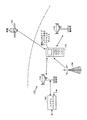
図3は、擬似八木タイプアンテナとして構成されるアンテナ302を含み、2つの接地面間にバラン304を含むアンテナ構造300を示す。アンテナ302は、ワイヤレスデバイス110のアンテナアレイ210〜212のような、アンテナアレイのうちの1つまたは複数のアンテナとすることができる。本明細書において用いられるときに、「アンテナ構造」は、バランおよびアンテナを含む構造と定義され、「アンテナ」は、電磁波が送信または受信される場合がある任意の導電性素子と定義され、「バラン」は、平衡信号(たとえば、差動信号)と不平衡信号(たとえば、シングルエンド信号)との間を変換する任意のデバイスと定義される。
FIG. 3 shows an
アンテナ302は、ダイポール部分306と、ダイポール部分306をバラン304に結合するワイヤ部分とを含む。バラン304は、入ってくる信号を受信し、ダイポール部分306に与えられる位相調整済み信号を生成することなどによって、不平衡信号を平衡信号に変換するように構成される。たとえば、バラン304は、入ってくる信号を受信する入力を有するように示されており、2つの信号経路の出力信号間に位相遅延を導入するために異なる長さの2つの信号経路を含む。出力信号はダイポール部分306に与えられる。ダイポール部分306は2つのダイポール「アーム」を含む。各ダイポールアームは、バラン304のそれぞれの信号経路に結合される。 The antenna 302 includes a dipole portion 306 and a wire portion that couples the dipole portion 306 to the balun 304. Balun 304 is configured to convert an unbalanced signal into a balanced signal, such as by receiving an incoming signal and generating a phase adjusted signal that is provided to dipole portion 306. For example, the balun 304 is shown as having an input that receives an incoming signal and includes two signal paths of different lengths to introduce a phase delay between the output signals of the two signal paths. The output signal is provided to dipole portion 306. Dipole portion 306 includes two dipole “arms”. Each dipole arm is coupled to a respective signal path of balun 304.
アンテナ302の少なくとも一部(たとえば、ダイポール部分306とバラン304との間のワイヤ部分の一部)は、第1の接地面(ground plane)310(たとえば、上側接地面)と第2の接地面312(たとえば、下側接地面)との間にあるモジュールの内層(inner layer)311内に配置される。代替的には、接地面間の層は中間層(interlayer)と呼ばれる場合もある。接地面310、312は、PC基板のような基板の表面または内側層(interior layer)に位置することができる。複数のビアが導電性「ビア壁」314を形成することができ、ビア壁は2つの接地面310、312を互いに結合し、ダイポール部分306の反射体として機能する。
At least a portion of the antenna 302 (e.g., a portion of the wire portion between the dipole portion 306 and the balun 304) includes a first ground plane 310 (e.g., an upper ground plane) and a second ground plane. Arranged in an inner layer 311 of the module between 312 (eg, the lower ground plane). Alternatively, the layer between the ground planes is sometimes referred to as the interlayer. The ground planes 310, 312 may be located on the surface of a substrate, such as a PC substrate, or an interior layer. A plurality of vias can form a conductive “via wall” 314, which connects the two
アンテナ302は、ストリップ線路と、2つの接地面310、312間の内層311内に配置されるバラン給電線とを用いて給電される場合がある。たとえば、バラン304は、フォトリソグラフィおよび金属堆積プロセスを用いることによって、内層311の誘電体材料内に形成することができる。例示するために、誘電体材料は、下側接地面312上に堆積することができ、フォトリソグラフィおよび金属堆積プロセスを用いて、下側接地面312の上方にバラン304の導電性ワイヤパターンを形成することができ、バラン304の上方に上側接地面310を形成することができる。アンテナ給電線、導波路、伝送線路、コネクタなどの1つまたは複数の電気的構成要素313がバラン304に結合される場合もある。たとえば、アンテナ給電線は、同調器ユニットおよび/またはインピーダンス整合構成要素を含むことができ、アンテナへの信号の送信またはアンテナからの信号の受信中に、受信信号を調整するように動作することができる。低損失電波伝送媒体を設けることによって、コプレーナ導波路のような導波路が動作することができる。アンテナへの、またはアンテナからの伝搬経路を設けることによって、マイクロストリップまたはストリップ線路のような伝送線路が動作することができる。バランと、増幅器(たとえば、図2のLNA240paまたはPA254pa)のような別の構成要素との間で信号が伝搬できるようにする接続を設けることによって、コネクタが動作することができる。
The antenna 302 may be fed using a strip line and a balun feed line disposed in the inner layer 311 between the two
図3に示されるような、擬似八木タイプアンテナは、2つの接地面にもかかわらず効率的に放射する。たとえば、擬似八木タイプアンテナはRFモジュールに含まれる場合があり、ビア壁314のビアは、特定の放射を反射する場所に配置される場合があるが、RFモジュールの外部に信号を放射できるようにする開口部も有する。接地面310、312はそれぞれ、接地面310、312の反対側にあるアンテナ間の干渉を減衰させるか、または解消するために電磁遮蔽を与えることができる。モジュールの内層内に含まれるアンテナを(図示されるように)設計する結果として、面積当たりのアンテナ密度を高くすることができる。たとえば、図4〜図5に関してさらに説明されるように、アンテナを複数の層に「積重する(stacking)」ことによってアンテナ密度を高めることができ、それらの層は、積重体(stack)内のアンテナ間の干渉を低減するために接地面によって分離される。 The pseudo Yagi type antenna as shown in FIG. 3 radiates efficiently despite two ground planes. For example, a pseudo-Yagi type antenna may be included in the RF module, and the vias in the via wall 314 may be placed where specific radiation is reflected, but can radiate signals outside the RF module. It also has an opening for The ground planes 310, 312 can provide electromagnetic shielding to attenuate or eliminate interference between antennas on the opposite side of the ground planes 310, 312, respectively. As a result of designing the antennas contained in the inner layer of the module (as shown), the antenna density per area can be increased. For example, as further described with respect to FIGS. 4-5, antenna density can be increased by “stacking” the antennas into multiple layers, which layers are stacked within the stack. Are separated by a ground plane to reduce interference between the two antennas.
図4は、複数の擬似八木タイプアンテナ402、404、406、452および454を含む例示的なRFモジュール430を示す。擬似八木タイプアンテナはそれぞれ、第1の接地面410と第2の接地面412との間のRFモジュール430の内層411内に存在する。第1の接地面410および第2の接地面412は、擬似八木タイプアンテナと、RFモジュール430の上面および下面上の構成要素との間の干渉を低減するために、放射を遮断することができる。たとえば、パッチアンテナのような他のアンテナ460〜465が接地面の外層上(たとえば、第1の接地面410がパッチアンテナと、擬似八木タイプアンテナのバラン480〜484との間にあるような第1の接地面410上)に位置することができる。
FIG. 4 shows an
複数の擬似八木タイプアンテナ素子は、第1の接地面410および第2の接地面412の外側に配置される(たとえば、RFモジュール430のエッジ面から外側に突出する)ダイポール部分を有し、それらのダイポール部分は、接地面410、412間に配置されるバランに結合される。ダイポールのうちの1つまたは複数のための反射体として機能するビア壁414が接地面410、412間に位置決めされる場合がある。
The plurality of pseudo-Yagi type antenna elements have dipole portions disposed outside the
RFモジュール430の異なるエッジに隣接して、複数組の擬似八木タイプアンテナが形成される場合がある。たとえば、第1の組440のアンテナ素子がアンテナ402、404および406を含むことができ、第2の組442のアンテナ素子がアンテナ452および454を含むことができ、各アンテナは、図示されるように、それぞれのバラン480〜484に結合される場合がある。RFモジュール430の2つのエッジに沿って2組の擬似八木タイプアンテナを有するRFモジュール430が例示されるが、他の実施態様では、3組以上の擬似八木タイプアンテナが含まれる場合がある。たとえば、4組の擬似八木タイプアンテナが含まれる場合があり、RFモジュール430の4つのエッジが擬似八木タイプアンテナを含むように、各組がRFモジュール430のそれぞれのエッジに隣接する場合がある。
Multiple sets of pseudo-Yagi type antennas may be formed adjacent to different edges of the
RFモジュール430は単層の擬似八木タイプアンテナを有するように示されるが、図5に関してさらに詳細に説明されるように、接地面によって分離される擬似八木タイプアンテナの更なる層がRFモジュール内に含まれる場合がある。いくつかの実施形態では、1つのRFモジュール内に3つ以上のアンテナ層が含まれる場合がある。
Although
RFモジュール430は、複数のRFチェーン470〜474を含む無線周波数集積回路(RFIC)450(たとえば、混合器、増幅器など)に結合される場合がある。たとえば、RFIC450内に「N」個のRFチェーン470〜474が含まれる場合があり、ただし、Nは1より大きい任意の正の整数である。RFIC450内の少なくとも1つのRFチェーン470〜474は、複数のアンテナ素子(たとえば、擬似八木タイプアンテナ402、404、406、452および454)の第1のアンテナ素子に結合される場合がある。第2の接地面412は、RFモジュール430の下側接地面とすることができる。第2の接地面412は、RFIC450とバラン480〜484との間に配置される場合があり、RFモジュール430のアンテナとRFIC450の構成要素との間の干渉を低減することができる。RFIC450はRFモジュール430(たとえば、PC基板)の下方に示され、RFモジュール430より厚いように示されるが、他の実施形態では、RFIC450は、RFモジュール430に対して別の位置を有することができ(たとえば、隣接する、上方にあるなど)、RFモジュール430に対して異なる厚さを有することができる(たとえば、RFモジュール430と実質的に等しい厚さ、またはRFモジュール430より薄い)。RFチェーン470〜474は、RFモジュール430の個々のアンテナ素子に結合される場合がある。
The
RFモジュール430のアンテナ(擬似八木タイプアンテナ402〜406および452〜454、ならびにアンテナ460〜465のような他のタイプのアンテナを含む)は、別々に、または1つまたは複数のアレイの一部として動作することができる。一群のアンテナがアンテナアレイとして動作するとき、アレイの各アンテナは、ビームフォーミングのためにRFモジュール430内のそれぞれの移相器に結合される場合がある。たとえば、RFモジュール430は、複数の移相器を含むことができる。アンテナアレイの各アンテナは、それぞれの移相器に結合することができる。たとえば、パッチアンテナ460〜465はそれぞれ1つの移相器に結合することができ、擬似八木タイプアンテナ402、404、406、452および454はそれぞれ1つの移相器に結合することができる。移相器はそれぞれアンテナアレイの1つのアンテナによって送信されることになる信号を受信し、信号に位相オフセットを導入するように構成することができる。移相器によって生成される各位相シフト済み信号は、アンテナによって送信するために、移相器に結合されるアンテナに与えられる。アレイ内の複数のアンテナから結果として生じる位相シフト済み送信は、送信される信号内に強め合う干渉および弱め合う干渉を引き起こし、結果として、指向性の信号送信(たとえば、ビームフォーミング)をもたらすことができる。
The
擬似八木タイプアンテナおよび他のアンテナ460〜465(たとえば、パッチアンテナ)のような複数のタイプのアンテナがRFモジュール430に含まれる場合があるので、1つのタイプのアンテナを用いる場合と比べて、広い信号カバレッジを与えることができる。たとえば、1つまたは複数のアンテナアレイが複数のタイプのアンテナを含むことができ、複数のアンテナが異なる放射パターンを有し、異なる指向性を与えることができる。アンテナアレイ内の多様なアンテナ位置、アンテナ方位、およびアンテナタイプが、そのアンテナアレイのための改善された全体カバレッジを与えることができる。
Multiple types of antennas such as pseudo-Yagi type antennas and other antennas 460-465 (for example, patch antennas) may be included in the
第1の接地面410上にアンテナ460〜465を有するようなRFモジュール430が示されるが、他の実施形態では、1つまたは複数の表面実装技術(SMT)構成要素のような他のデバイスが第1の接地面410上に実装される場合がある。たとえば、SMT構成要素は、RFモジュール430の表面に実装される1つまたは複数の導体、1つまたは複数のキャパシタ、および/または集積回路(IC)を含むことができる。RFモジュール430の表面上にSMT構成要素を実装することによって、少ないコストで、よりコンパクトなPCBを可能にすることができる。
Although an
RFモジュール430の1つのエッジに沿って3つの擬似八木タイプアンテナ402〜406が示され、RFモジュール430の別のエッジに沿って2つの擬似八木タイプアンテナ402〜406が示され、図4の第1の接地面410上に6つの他のアンテナ460〜465が示されるが、空間の利用可能性および設計制約に応じて、エッジのいずれかに、および/またはRFモジュール430の任意の表面上に任意の数のアンテナを配置することができる。いくつかの実施態様では、RFチェーン470〜474の数がRFモジュール430のアンテナの数に等しく、各RFチェーンがそれぞれのアンテナを専用に使用するが、他の実施形態では、RFチェーンの数はアンテナの数とは異なり、RFチェーンを選択的にアンテナに結合するか、またはアンテナから切り離すために、スイッチング回路(たとえば、高速クロスバー)が用いられる場合がある。
Four pseudo Yagi type antennas 402-406 are shown along one edge of the
接地面410、412間に複数の擬似八木タイプアンテナを含むことによって、アンテナ密度を改善するために、RFモジュール430の一部として、更なるアンテナ460〜465を含むこともできる。アンテナカバレッジ、およびビームフォーミングのようなアンテナアレイ応用例は、単一のRFモジュール430内で多様なアンテナ方位、アンテナ位置およびアンテナタイプを用いることによって向上させることができる。したがって、図4は、高いアンテナ密度を与え、広いアンテナカバレッジおよび高度なアンテナアレイ応用例を提供することができるRFモジュールを示す。
Additional antennas 460-465 may also be included as part of the
図5は、複数の接地面と、接地面間にアンテナとを含むモジュール500の例示的な実施形態を示す。第1の接地面510および第2の接地面512はそれぞれ、モジュール500の上側接地面および下側接地面とすることができる。第3の接地面514が、上側接地面(510)と下側接地面(512)との間に位置決めされる。
FIG. 5 illustrates an exemplary embodiment of a
第1の複数のアンテナ素子540が第1の複数のバラン542に結合される。第1の複数のバラン542の各バランは、第1の接地面510と第3の接地面514との間の第1の内層511内に配置される。第1の複数のアンテナ素子540のうちの第1の組のアンテナ素子は、第1の内層511の第1のエッジ591に隣接して位置することができる。たとえば、第1の組のアンテナ素子のダイポールは、第1の内層511の第1のエッジ591から外側に延在し、同じく第1のエッジ591付近に位置決めされるそれぞれのバランに結合される。第1の複数のアンテナ素子540のうちの第2の組のアンテナ素子(図示せず)は、第1の内層511の第2のエッジ592に隣接して位置することができる。たとえば、第1の組および第2の組のアンテナ素子は、図4に示される第1の組440および第2の組442のアンテナ素子に対応することができる。第2の複数のアンテナ素子544が第2の複数のバラン546に結合される。第2の複数のバラン546の各バランは、第3の接地面514と第2の接地面512との間の第2の内層513内に配置される。
A first plurality of antenna elements 540 are coupled to the first plurality of baluns 542. Each balun of the first plurality of baluns 542 is disposed in the first inner layer 511 between the
図5は単一の接地面によって分離される2つの擬似八木タイプアンテナ層を示すが、他の実施形態では、1つのモジュール内で3つ以上のアンテナ層が複数の接地面によって分離される場合がある。その代わりに、またはそれに加えて、図4に示されるのと同様に第1の接地面510の上面上のパッチアンテナのような、1つまたは複数の他のタイプのアンテナが含まれる場合もある。モジュール500は、図4のRFIC450のようなRFICに接続することができる。たとえば、モジュール500は、接地面510、512、514を通して信号をRFモジュール500内の異なる層にあるアンテナに転送できるようにするビアまたは他の導電性構造を含むことができる。接地面間の内層内にアンテナを位置決めすることによって、単一のアンテナ層を用いる場合と比べて、高いアンテナ密度を与えるためにモジュール500内にいくつかのアンテナを積重することができる。
FIG. 5 shows two pseudo-Yagi type antenna layers separated by a single ground plane, but in other embodiments, more than two antenna layers are separated by multiple ground planes in a module There is. Alternatively or in addition, one or more other types of antennas may be included, such as a patch antenna on the top surface of the
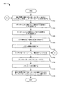
図6は、図3のアンテナ構造300のような擬似八木タイプアンテナを設計するための例示的で、非限定的な方法を示す。602において、ダイポールの全長(たとえば、図3のダイポール部分306の先端間の距離)がある値に設定され、その値は、波長(λ)を2で割った値(λ/2)に等しい場合がある。たとえば、波長は、擬似八木タイプアンテナによって送信されることになる信号の波長(たとえば、60GHzの場合、約5ミリメートル(mm)の波長)に対応することができる。ダイポールの全長に基づいて、ダイポールアーム間の最小間隔が規定され、ダイポールアーム長が計算される。604において、ダイポールから接地されたビア壁までの距離(たとえば、図3のビア壁314と、ダイポール部分306のアームとの間の距離)が、λ/4に設定される。606において、ダイポールから誘電体エッジまでの距離がλ/4に設定される。608において、ビア壁内のビア間の分離距離が設定される。たとえば、分離距離は、製造技術によって規定される最小許容ビア分離に設定することができる。
FIG. 6 illustrates an exemplary, non-limiting method for designing a pseudo-Yagi type antenna, such as the
610において、接地エッジからのバラン距離(たとえば、バラン304と、下側接地面312の上面との間の分離)が、2つの信号経路に沿ってダイポールまで信号が伝搬する結果として生じる差動モードの品質が差動信号品質しきい値を満たすように規定される。たとえば、バラン304は、ダイポール部分306の2つのアームにおいて信号「V1」と「V2」との間に実質的に180度の位相シフトを生成するように設計することができ、信号V1およびV2は実質的に等しい振幅を有する。差動信号の品質は、コモンモード(V1+V2)/2と差動モード(V1-V2)/2との比によって規定することができる。理想的な差動信号は0コモンモード(すなわち、V1=-V2)を有する。バランと接地面との間の分離は、差動信号の品質が差動信号品質しきい値以上であるように設定することができる。612において、決定されたダイポールアーム長、ダイポールアーム間の間隔、ビア壁とダイポールアームとの間の距離、および接地面とバランとの間の分離を有する結果として形成されたアンテナがシミュレートされ、チェック照合が実行される。結果として形成されたアンテナのシミュレーションに基づいて、十分な帯域幅に達しない場合には、より広い整合のためにバランと接地面との間の分離を大きくする、より低い中心周波数またはより高い中心周波数に達するようにダイポール長を増減する、および/または他のパラメータを調整するなどの、上記の1つまたは複数のパラメータを調整することができ、その後、処理を継続するために602に戻ることができる。 At 610, a differential mode where the balun distance from the ground edge (e.g., the separation between the balun 304 and the upper surface of the lower ground plane 312) results in the signal propagating along the two signal paths to the dipole. Is defined to meet a differential signal quality threshold. For example, the balun 304 can be designed to produce a substantially 180 degree phase shift between the signals “V1” and “V2” in the two arms of the dipole portion 306, where the signals V1 and V2 are Have substantially equal amplitudes. The quality of the differential signal can be defined by the ratio between the common mode (V1 + V2) / 2 and the differential mode (V1-V2) / 2. An ideal differential signal has 0 common mode (ie, V1 = −V2). The separation between the balun and the ground plane can be set such that the quality of the differential signal is greater than or equal to the differential signal quality threshold. At 612, the resulting antenna having the determined dipole arm length, the distance between the dipole arms, the distance between the via wall and the dipole arm, and the separation between the ground plane and the balun is simulated, Check verification is performed. Based on simulation of the resulting antenna, a lower center frequency or higher center that increases the separation between the balun and ground plane for wider matching if sufficient bandwidth is not reached One or more of the above parameters can be adjusted, such as increasing or decreasing the dipole length to reach the frequency, and / or adjusting other parameters, then returning to 602 to continue processing Can do.
シミュレーションに基づいて、十分な帯域幅に達すると、614において、アンテナパターン(すなわち、アンテナからの方向変位の関数としてのアンテナからの放射信号強度)がシミュレートされる。616において、接地サイズ、接地までの距離、誘電体エッジまでの距離、および/またはビア距離を変更して、アンテナパターンを調整するか、または「同調させる」ことができる。いくつかの実施形態では、アンテナに1つまたは複数の導波器(director)(たとえば、八木タイプ共振器素子)を追加して、アンテナサイズが大きくなることと引き換えに、高い利得が得られるようにアンテナ放射パターンを変更することができる。618において、整合が影響を受けないことを検証するために、アンテナパターンシミュレーションが(616における調整後に)繰り返される。整合が影響を受けた場合には、パターンおよび整合を同時に調整することができる。たとえば、ダイポールアーム長、および接地面からの距離のようないくつかのアンテナパラメータが、アンテナパターンおよび整合の両方に影響を及ぼす。他のアンテナパラメータは、ダイポールに給電する伝送線路の幅のように、主に整合に影響を及ぼすか、または異なるダイポールアンテナ間の距離のように、主にパターンに主に影響を及ぼす。パターン調整のためのパラメータを調整することは整合に影響を及ぼす場合があるので、整合に主に(またはもっぱら)影響を及ぼす1つまたは複数の他のパラメータを調整して、整合を再調整することもできる。同様に、整合に関するパラメータを調整することは、アンテナパターンに影響を及ぼす場合があり、アンテナパターンに主に(またはもっぱら)影響を及ぼす1つまたは複数の他のパラメータを調整して、パターンを再調整することもできる。それゆえ、アンテナパターンおよび整合を同時に調整することは、複数のパラメータを調整することを含む場合がある。 Based on simulation, when sufficient bandwidth is reached, the antenna pattern (ie, the intensity of the radiated signal from the antenna as a function of directional displacement from the antenna) is simulated at 614. At 616, the antenna pattern can be adjusted or “tuned” by changing the ground size, the distance to ground, the distance to the dielectric edge, and / or the via distance. In some embodiments, one or more directors (e.g., Yagi type resonator elements) can be added to the antenna to achieve higher gain at the expense of increased antenna size. The antenna radiation pattern can be changed. At 618, the antenna pattern simulation is repeated (after adjustment at 616) to verify that the alignment is not affected. If alignment is affected, the pattern and alignment can be adjusted simultaneously. For example, several antenna parameters such as dipole arm length and distance from the ground plane affect both antenna pattern and alignment. Other antenna parameters mainly affect the alignment, such as the width of the transmission line feeding the dipole, or mainly the pattern, such as the distance between different dipole antennas. Adjusting parameters for pattern adjustments can affect alignment, so adjust one or more other parameters that primarily (or exclusively) affect alignment and readjust the alignment You can also. Similarly, adjusting parameters related to matching can affect the antenna pattern, and adjust one or more other parameters that primarily (or exclusively) affect the antenna pattern to recreate the pattern. It can also be adjusted. Therefore, adjusting the antenna pattern and matching simultaneously may include adjusting multiple parameters.
図7は、ワイヤレスデバイス110における送信のような、ワイヤレスデバイスの動作方法700の流れ図を示す。方法700は、702において、2つの接地面間にあるアンテナ構造のバランにおいて信号を受信することを含むことができる。たとえば、図4のRFIC450のような、無線周波数回路から信号が受信される場合がある。例示するために、信号は60GHzワイヤレス信号とすることができる。信号は、図3のバラン304(上側接地面310と下側接地面312との間のバラン304)において受信される場合がある。
FIG. 7 shows a flowchart of a
方法700は、704において、バランの出力において位相調整済み信号を生成することと、706において、擬似八木タイプアンテナを用いて位相調整済み信号を放射することとを含むこともできる。たとえば、位相調整済み信号は、図3のバラン304において生成される場合がある。例示するために、バラン304は、バラン304から出力される2つの信号に位相差を導入するために、第1の経路および第2の経路を介して受信信号(たとえば、60GHz信号)を分割することができ、ただし、第2の経路は第1の経路より長い経路長を有する。バランから出力される2つの信号は、信号をワイヤレス送信するために、アンテナダイポールのそれぞれのダイポールアームに与えることができる。アンテナは擬似八木タイプアンテナとすることができ、図3のビア壁314のような、接地面を接続するビア壁によって形成される反射体を含むことができる。
The
その方法は、パッチアンテナにおいて第2の信号を放射することを含むこともできる。たとえば、接地面のうちの1つがアンテナ構造とパッチアンテナとの間に存在することができる。たとえば、第1の接地面410は、擬似八木タイプアンテナ402のようなアンテナ構造と、図4の擬似八木タイプアンテナ402および他のアンテナ460に結合されるバランとの間に存在することができる。第2の信号は、アンテナ構造(たとえば、バランに結合される擬似八木タイプアンテナ)およびパッチアンテナを含むアンテナアレイにおいてビームフォーミングが実行されるときのような、第1の信号の位相シフトバージョンに対応することができる。代替的には、第2の信号は、アンテナ構造およびパッチアンテナが異なるワイヤレスネットワーク(たとえば、60GHz広帯域データネットワークおよびCDMAタイプ音声ネットワーク)に異なるデータを送信するときのように、第1の信号から独立している場合がある。
The method can also include radiating a second signal at the patch antenna. For example, one of the ground planes can exist between the antenna structure and the patch antenna. For example, the
受信動作中に、発振する電磁場(たとえば、ワイヤレス信号)が、アンテナの各ダイポールアーム内に信号を誘導することができる(たとえば、誘導される交流)。信号は、バランの出力信号を生成するために、バランによって互いに対して位相シフトされ、合成される(たとえば、加算される)場合がある。バランによって出力される信号は、データプロセッサによって処理する前に、フィルタリングおよびベースバンド変換のために、受信チェーンに与えることができる。 During a receive operation, an oscillating electromagnetic field (eg, a wireless signal) can induce a signal in each dipole arm of the antenna (eg, induced alternating current). The signals may be phase shifted with respect to each other by the balun and combined (eg, summed) to produce a balun output signal. The signal output by the balun can be provided to the receive chain for filtering and baseband conversion before processing by the data processor.
接地面の対間にバランを位置決めすることによって、高いアンテナ密度を達成できるようになる。たとえば、接地面は、RFモジュールの表面層にあるパッチアンテナから、またはRFモジュールの他の内層にある他のエッジアンテナから、のように、接地面がなければ他の層にあるアンテナにおける信号送信から生じる場合がある、バランにおける干渉を低減する。 By positioning the balun between a pair of ground planes, a high antenna density can be achieved. For example, if the ground plane is from a patch antenna on the surface layer of the RF module, or from another edge antenna on the other inner layer of the RF module, signal transmission on the antenna on the other layer if there is no ground plane Reduce interference in the balun, which may arise from
説明された実施形態に関連して、装置は、信号を放射するための手段を含む。たとえば、信号を放射するための手段は、図3のダイポール306、図5の第1の複数のアンテナ素子540または第2の複数のアンテナ素子544のうちの1つまたは複数、1つまたは複数の他のデバイス、回路、あるいはその任意の組合せを含むことができる。 In connection with the described embodiment, the apparatus includes means for emitting a signal. For example, the means for radiating the signal may include one or more, one or more of the dipole 306 of FIG. 3, the first plurality of antenna elements 540 or the second plurality of antenna elements 544 of FIG. Other devices, circuits, or any combination thereof can be included.
その装置は、放射するための手段の入力に結合される位相調整済み信号を生成するための手段を含む。たとえば、生成するための手段は、図3のバラン304、図5の第1の複数のバラン542または第2の複数のバラン544のうちの1つまたは複数、1つまたは複数の他のデバイス、回路、あるいはその任意の組合せを含むことができる。 The apparatus includes means for generating a phase adjusted signal coupled to the input of the means for radiating. For example, the means for generating include one or more of the balun 304 of FIG. 3, the first plurality of baluns 542 or the second plurality of baluns 544 of FIG. 5, one or more other devices, A circuit, or any combination thereof, can be included.
その装置は、生成するための手段を接地するための第1の手段と、生成するための手段を接地するための第2の手段とを含む。生成するための手段は、接地するための第1の手段と接地するための第2の手段との間に配置される。たとえば、接地するための第1の手段は、図3の上側接地面310または下側接地面312、図4の上側接地面410または下側接地面412、または図5の第1の接地面510、第2の接地面512または第3の接地面514を含むことができる。接地するための第2の手段は、図3の上側接地面310または下側接地面312、図4の上側接地面410または下側接地面412、または図5の第1の接地面510、第2の接地面512または第3の接地面514を含むことができる。
The apparatus includes a first means for grounding the means for generating and a second means for grounding the means for generating. The means for generating is disposed between the first means for grounding and the second means for grounding. For example, the first means for grounding may be the
その装置は、擬似八木タイプアンテナ構造を形成することができる。接地するための手段はそれぞれ、接地するための手段(図3の接地面310または312)の反対面上のアンテナ構造間の干渉を減衰させるか、または解消することができる。モジュールの内層に少なくとも部分的に含まれるアンテナ構造を設計する結果として、アンテナ密度を高めることができる。たとえば、図4〜図5に関して説明されたように、接地面によって分離される層においてアンテナを「積重する」ことによって、アンテナ密度を高めることができる。
The device can form a pseudo-Yagi type antenna structure. Each means for grounding can attenuate or eliminate interference between antenna structures on the opposite side of the means for grounding (
当業者はさらに、本明細書において開示される実施形態に関連して説明された種々の例示的な論理ブロック、構成、モジュール、回路、およびアルゴリズムステップが、電子ハードウェア、プロセッサによって実行されるコンピュータソフトウェア、または両方の組合せとして実現できることは理解されよう。種々の例示的な構成要素、ブロック、構成、モジュール、回路、およびステップは、これまで、それらの機能の観点から包括的に説明されてきた。そのような機能が、ハードウェアとして実現されるか、プロセッサ実行可能命令として実現されるかは、特定の適用例と、システム全体に課される設計制約とによって決まる。当業者は、説明された機能を特定のアプリケーションごとに種々の方法で実現することができるが、そのような実施態様の決定は、本開示の範囲からの逸脱を引き起こすと解釈されるべきではない。 Those skilled in the art further recognize that the various exemplary logic blocks, configurations, modules, circuits, and algorithm steps described in connection with the embodiments disclosed herein are executed by electronic hardware, a processor, and a computer. It will be appreciated that it can be implemented as software, or a combination of both. Various illustrative components, blocks, configurations, modules, circuits, and steps have been comprehensively described above in terms of their functionality. Whether such functionality is implemented as hardware or processor-executable instructions depends on the particular application and design constraints imposed on the overall system. Those skilled in the art can implement the described functionality in a variety of ways for each particular application, but such implementation decisions should not be construed as causing a departure from the scope of this disclosure. .
本明細書で開示する例示的な実施形態に関して説明する方法またはアルゴリズムのステップは、直接ハードウェアで、プロセッサによって実行されるソフトウェアモジュールで、またはその2つの組合せで具現化されてよい。ソフトウェアモジュールは、ランダムアクセスメモリ(RAM)、フラッシュメモリ、読取り専用メモリ(ROM)、プログラム可能読取り専用メモリ(PROM)、消去可能プログラム可能読取り専用メモリ(EPROM)、電気的消去可能プログラム可能読取り専用メモリ(EEPROM)、レジスタ、ハードディスク、リムーバブルディスク、コンパクトディスク読取り専用メモリ(CD-ROM)、または当技術分野において既知の任意の他の形の非一時的記憶媒体内に存在することができる。例示的な記憶媒体は、プロセッサが記憶媒体から情報を読み取り、記憶媒体に情報を書き込むことができるように、プロセッサに結合される。代替形態では、記憶媒体は、プロセッサと一体に構成することができる。プロセッサおよび記憶媒体は特定用途向け集積回路(ASIC)内に存在することができる。ASICは、コンピューティングデバイスまたはユーザ端末内に存在することができる。代替形態では、プロセッサおよび記憶媒体は、コンピューティングデバイスまたはユーザ端末内に個別の構成要素として存在することができる。 The method or algorithm steps described in connection with the exemplary embodiments disclosed herein may be implemented directly in hardware, in software modules executed by a processor, or in a combination of the two. Software modules include random access memory (RAM), flash memory, read only memory (ROM), programmable read only memory (PROM), erasable programmable read only memory (EPROM), electrically erasable programmable read only memory (EEPROM), registers, hard disk, removable disk, compact disk read only memory (CD-ROM), or any other form of non-transitory storage medium known in the art. An exemplary storage medium is coupled to the processor such that the processor can read information from, and write information to, the storage medium. In the alternative, the storage medium may be integral to the processor. The processor and the storage medium can reside in an application specific integrated circuit (ASIC). The ASIC can reside in a computing device or user terminal. In the alternative, the processor and the storage medium may reside as discrete components in a computing device or user terminal.
開示される実施形態のこれまでの説明は、当業者が開示される実施形態を作製または使用できるようにするために提供される。これらの実施形態に対する種々の変更は、当業者には容易に明らかになり、本明細書において規定された原理は、本開示の範囲から逸脱することなく、他の実施形態に適用することができる。したがって、本開示は、本明細書に示される実施形態に限定されることを意図するものではなく、以下の特許請求の範囲によって規定される原理および新規な特徴と一致する、取り得る最も広い範囲を与えられるべきである。 The previous description of the disclosed embodiments is provided to enable any person skilled in the art to make or use the disclosed embodiments. Various modifications to these embodiments will be readily apparent to those skilled in the art, and the principles defined herein may be applied to other embodiments without departing from the scope of the disclosure. . Accordingly, the present disclosure is not intended to be limited to the embodiments shown herein, but is to be accorded the widest possible scope consistent with the principles and novel features defined by the following claims. Should be given.
110 ワイヤレスデバイス
120 ワイヤレス通信システム
130 基地局
132 基地局
134 放送局
140 システムコントローラ
150 衛星
210 一次アンテナアレイ
212 二次アンテナアレイ
220 送受信機
222 送受信機
224 アンテナインターフェース回路
226 アンテナインターフェース回路
230 受信機
230pa 受信機
230sa 受信機
230pk 受信機
230sl 受信機
240 LAN
240pa LAN
242 受信回路
242pa 受信回路
250 送信機
250pa 送信機
250sa 送信機
250pk 送信機
250sl 送信機
252 送信回路
252pa 送信回路
254 電力増幅器(PA)
254pa PA
280 データプロセッサ/コントローラ
282 メモリ
300 アンテナ構造
302 アンテナ
304 バラン
306 ダイポール部分
310 第1の接地面
311 内層
312 第2の接地面
314 ビア壁
402 擬似八木タイプアンテナ
404 擬似八木タイプアンテナ
406 擬似八木タイプアンテナ
410 第1の接地面
411 内層
412 第2の接地面
430 RFモジュール
440 第1の組のアンテナ素子
442 第2の組のアンテナ素子
450 無線周波数集積回路(RFIC)
452 擬似八木タイプアンテナ
454 擬似八木タイプアンテナ
460 他のアンテナ
465 他のアンテナ
470 RFチェーン
474 RFチェーン
480 バラン
484 バラン
500 モジュール
510 第1の接地面
511 第1の内層
512 第2の接地面
513 第2の内層
514 第3の接地面
540 第1の複数のアンテナ素子
542 第1の複数のバラン
544 第2の複数のアンテナ素子
546 第2の複数のバラン
591 第1のエッジ
110 wireless devices
120 wireless communication system
130 base station
132 Base station
134 broadcast station
140 System controller
150 satellites
210 Primary antenna array
212 Secondary antenna array
220 transceiver
222 Transceiver
224 Antenna interface circuit
226 Antenna interface circuit
230 Receiver
230pa receiver
230sa receiver
230pk receiver
230sl receiver
240 LAN
240pa LAN
242 Receiver circuit
242pa receiver circuit
250 transmitter
250pa transmitter
250sa transmitter
250pk transmitter
250sl transmitter
252 Transmitter circuit
252pa transmitter circuit
254 Power Amplifier (PA)
254pa PA
280 Data Processor / Controller
282 memory
300 Antenna structure
302 antenna
304 balun
306 Dipole part
310 First ground plane
311 Inner layer
312 Second ground plane
314 Beer Wall
402 Pseudo Yagi type antenna
404 Pseudo Yagi type antenna
406 Pseudo Yagi type antenna
410 First ground plane
411 Inner layer
412 Second ground plane
430 RF module
440 First set of antenna elements
442 Second set of antenna elements
450 Radio Frequency Integrated Circuit (RFIC)
452 Pseudo Yagi type antenna
454 Pseudo Yagi type antenna
460 other antennas
465 Other antennas
470 RF chain
474 RF chain
480 balun
484 Balun
500 modules
510 First ground plane
511 First inner layer
512 Second ground plane
513 Second inner layer
514 Third ground plane
540 first plurality of antenna elements
542 first multiple baluns
544 second plurality of antenna elements
546 Second multiple baluns
591 1st edge
Claims (20)
第1の接地面と、
第2の接地面と、
アンテナと、
前記アンテナに結合されるバランであって、前記バランは前記第1の接地面と前記第2の接地面との間に配置される、バランと
を備える、装置。 A device,
A first ground plane;
A second ground plane;
An antenna,
A balun coupled to the antenna, the balun comprising: a balun disposed between the first ground plane and the second ground plane.
アンテナ構造のバランにおいて信号を受信するステップであって、前記バランは2つの接地面間にある、受信するステップと、
前記バランの出力において位相調整済み信号を生成するステップと、
前記アンテナ構造を介して前記位相調整済み信号を放射するステップと
を含む、通信の方法。 A communication method,
Receiving a signal in a balun of an antenna structure, wherein the balun is between two ground planes;
Generating a phase adjusted signal at the output of the balun;
Radiating the phase adjusted signal through the antenna structure.
信号を放射するための手段と、
前記放射するための手段に結合される位相調整済み信号を生成するための手段と、
前記生成するための手段を接地するための第1の手段と、
前記生成するための手段を接地するための第2の手段と
を備え、前記生成するための手段は前記接地するための第1の手段と前記接地するための第2の手段との間に配置される、装置。 A device,
Means for emitting a signal;
Means for generating a phase adjusted signal coupled to the means for emitting;
First means for grounding said means for generating;
Second means for grounding the means for generating, the means for generating disposed between the first means for grounding and the second means for grounding Device.
Applications Claiming Priority (5)
| Application Number | Priority Date | Filing Date | Title |
|---|---|---|---|
| US201461925011P | 2014-01-08 | 2014-01-08 | |
| US61/925,011 | 2014-01-08 | ||
| US14/561,680 | 2014-12-05 | ||
| US14/561,680 US9912071B2 (en) | 2014-01-08 | 2014-12-05 | Quasi-yagi-type antenna |
| PCT/US2014/069105 WO2015105605A1 (en) | 2014-01-08 | 2014-12-08 | Quasi-yagi-type antenna |
Publications (2)
| Publication Number | Publication Date |
|---|---|
| JP2017502606A true JP2017502606A (en) | 2017-01-19 |
| JP2017502606A5 JP2017502606A5 (en) | 2018-05-31 |
Family
ID=53495894
Family Applications (1)
| Application Number | Title | Priority Date | Filing Date |
|---|---|---|---|
| JP2016544657A Pending JP2017502606A (en) | 2014-01-08 | 2014-12-08 | Pseudo Yagi type antenna |
Country Status (7)
| Country | Link |
|---|---|
| US (1) | US9912071B2 (en) |
| EP (1) | EP3092682A1 (en) |
| JP (1) | JP2017502606A (en) |
| KR (1) | KR20160105870A (en) |
| CN (1) | CN105934851A (en) |
| BR (1) | BR112016015929A2 (en) |
| WO (1) | WO2015105605A1 (en) |
Cited By (2)
| Publication number | Priority date | Publication date | Assignee | Title |
|---|---|---|---|---|
| KR20190125908A (en) * | 2018-04-30 | 2019-11-07 | 삼성전기주식회사 | Antenna apparatus and antenna module |
| US10826172B2 (en) | 2018-04-30 | 2020-11-03 | Samsung Electro-Mechanics Co., Ltd. | Antenna apparatus and antenna module |
Families Citing this family (31)
| Publication number | Priority date | Publication date | Assignee | Title |
|---|---|---|---|---|
| US20140087781A1 (en) * | 2012-09-18 | 2014-03-27 | Laurent Desclos | Wireless communication system & related methods for use in a social network |
| US9570809B2 (en) | 2013-06-06 | 2017-02-14 | Qualcomm Incorporated | Techniques for designing millimeter wave printed dipole antennas |
| CN111342235B (en) | 2015-01-27 | 2022-11-04 | 奥特斯奥地利科技与系统技术有限公司 | Electronic component and method for manufacturing electronic component |
| CN107925442B (en) * | 2015-11-27 | 2021-04-23 | 佐藤控股株式会社 | Multilayer electromagnetic coupler device |
| US10063211B2 (en) | 2016-02-03 | 2018-08-28 | Qualcomm Incorporated | Compact bypass and decoupling structure for millimeter-wave circuits |
| US9711849B1 (en) * | 2016-02-19 | 2017-07-18 | National Chung Shan Institute Of Science And Technology | Antenna reconfigurable circuit |
| EP4340012A3 (en) * | 2016-04-28 | 2024-05-22 | AT & S Austria Technologie & Systemtechnik Aktiengesellschaft | Component carrier with integrated antenna arrangement, electronic apparatus, radio communication method |
| JP7056889B2 (en) * | 2017-01-20 | 2022-04-19 | ソニーセミコンダクタソリューションズ株式会社 | Antenna device and receiver |
| CN110178268B (en) | 2017-01-20 | 2021-10-08 | 索尼半导体解决方案公司 | Antenna device and receiver |
| US10256549B2 (en) | 2017-04-03 | 2019-04-09 | King Fahd University Of Petroleum And Minerals | Compact size, low profile, dual wideband, quasi-yagi, multiple-input multiple-output antenna system |
| WO2018199944A1 (en) | 2017-04-26 | 2018-11-01 | Sony Mobile Communications Inc. | Millimeter wave antenna |
| US10418722B2 (en) | 2017-04-27 | 2019-09-17 | Texas Instruments Incorporated | Dipole antenna arrays |
| US10763566B2 (en) | 2017-07-20 | 2020-09-01 | Apple Inc. | Millimeter wave transmission line structures |
| US11005161B2 (en) * | 2017-10-20 | 2021-05-11 | Qualcomm Incorporated | Multilayer bowtie antenna structure |
| KR101939047B1 (en) * | 2017-12-26 | 2019-01-16 | 삼성전기 주식회사 | Antenna module and dual-band antenna apparatus |
| WO2019136271A1 (en) * | 2018-01-05 | 2019-07-11 | Wispry, Inc. | Hybrid high gain antenna systems, devices, and methods |
| CN110854548B (en) * | 2018-08-21 | 2021-07-23 | 深圳富泰宏精密工业有限公司 | Antenna structure and wireless communication device with same |
| WO2020082361A1 (en) | 2018-10-26 | 2020-04-30 | 华为技术有限公司 | Wide-bandwidth antenna in package device |
| US11005184B2 (en) | 2018-11-29 | 2021-05-11 | Samsung Electro-Mechanics Co., Ltd. | Antenna apparatus |
| CN111244610B (en) * | 2018-11-29 | 2024-05-24 | 三星电机株式会社 | Antenna device |
| KR102133393B1 (en) * | 2019-01-04 | 2020-07-14 | 삼성전기주식회사 | Antenna apparatus |
| KR102125085B1 (en) * | 2018-11-29 | 2020-06-19 | 삼성전기주식회사 | Antenna apparatus |
| CN112201938B (en) * | 2018-11-29 | 2024-05-03 | 三星电机株式会社 | Antenna device and electronic apparatus |
| US11342663B2 (en) * | 2019-01-04 | 2022-05-24 | Samsung Electro-Mechanics Co., Ltd. | Antenna apparatus |
| CN111864407B (en) * | 2019-04-25 | 2021-08-27 | 大唐移动通信设备有限公司 | Quasi-yagi antenna array and millimeter wave base station equipment |
| CN112054313A (en) | 2019-06-06 | 2020-12-08 | 北京小米移动软件有限公司 | Antenna structure, electronic equipment, antenna structure array method and device |
| CN110224214A (en) * | 2019-06-06 | 2019-09-10 | 天通凯美微电子有限公司 | A kind of electronic equipment of aerial array and radio frequency front-end devices and integrated chip |
| CN112054312B (en) * | 2019-06-06 | 2022-10-18 | 北京小米移动软件有限公司 | Antenna structure and electronic device |
| CN112151940A (en) * | 2019-06-28 | 2020-12-29 | 深圳市超捷通讯有限公司 | Antenna structure and wireless communication device with same |
| US11404788B1 (en) * | 2020-02-28 | 2022-08-02 | Micro Mobio Corporation | Surface mount antenna elements for use in an antenna array |
| CN114006157B (en) * | 2021-10-27 | 2024-02-06 | 东南大学 | Planar quasi-yagi antenna based on substrate integrated waveguide and tapered gradient structure feed |
Citations (4)
| Publication number | Priority date | Publication date | Assignee | Title |
|---|---|---|---|---|
| GB765465A (en) * | 1952-05-08 | 1957-01-09 | Standard Telephones Cables Ltd | Improvements in or relating to radio wave guide systems |
| US4516132A (en) * | 1983-02-24 | 1985-05-07 | Cossar Electronics Limited | Antenna with a reflector of open construction |
| US20050219140A1 (en) * | 2004-04-01 | 2005-10-06 | Stella Doradus Waterford Limited | Antenna construction |
| JP2013534079A (en) * | 2010-05-24 | 2013-08-29 | サイビーム インコーポレイテッド | Symmetric stripline balun for radio frequency applications |
Family Cites Families (22)
| Publication number | Priority date | Publication date | Assignee | Title |
|---|---|---|---|---|
| DE2020192B2 (en) | 1970-04-24 | 1978-06-01 | Siemens Ag, 1000 Berlin Und 8000 Muenchen | Strip-line dipole radiator - has symmetrical conductor network formed by etching on dielectric carrier at right angles to reflector |
| US5274391A (en) | 1990-10-25 | 1993-12-28 | Radio Frequency Systems, Inc. | Broadband directional antenna having binary feed network with microstrip transmission line |
| US5532708A (en) * | 1995-03-03 | 1996-07-02 | Motorola, Inc. | Single compact dual mode antenna |
| US6114997A (en) * | 1998-05-27 | 2000-09-05 | Raytheon Company | Low-profile, integrated radiator tiles for wideband, dual-linear and circular-polarized phased array applications |
| JP3462102B2 (en) * | 1998-12-02 | 2003-11-05 | 三菱電機株式会社 | Array antenna |
| US6476773B2 (en) | 2000-08-18 | 2002-11-05 | Tantivy Communications, Inc. | Printed or etched, folding, directional antenna |
| US6924776B2 (en) * | 2003-07-03 | 2005-08-02 | Andrew Corporation | Wideband dual polarized base station antenna offering optimized horizontal beam radiation patterns and variable vertical beam tilt |
| CN2706886Y (en) * | 2004-04-06 | 2005-06-29 | 福登精密工业股份有限公司 | Layout structure of multi-frequency doublet antenna structure |
| US7973730B2 (en) * | 2006-12-29 | 2011-07-05 | Broadcom Corporation | Adjustable integrated circuit antenna structure |
| KR100771529B1 (en) | 2007-05-30 | 2007-10-30 | 이엠와이즈 통신(주) | Ultra-wideband balun and application module thereof |
| AU2009249558B2 (en) | 2008-05-23 | 2013-09-12 | Audiovox Corporation | Omni-directional, multi-polarity, low profile planar antenna |
| TWI358854B (en) | 2008-05-30 | 2012-02-21 | Univ Nat Taiwan Science Tech | Ultra high frequency planar antenna |
| US8232920B2 (en) * | 2008-08-07 | 2012-07-31 | International Business Machines Corporation | Integrated millimeter wave antenna and transceiver on a substrate |
| US8120545B2 (en) * | 2009-08-17 | 2012-02-21 | Auden Techno Corp. | Multifunctional antenna chip |
| US20120218156A1 (en) | 2010-09-01 | 2012-08-30 | Qualcomm Incorporated | On-frequency repeater |
| US20130082893A1 (en) | 2011-09-30 | 2013-04-04 | Raytheon Company | Co-phased, dual polarized antenna array with broadband and wide scan capability |
| JP6169395B2 (en) * | 2012-08-27 | 2017-07-26 | 株式会社トーキン | Resonator |
| US9112253B2 (en) * | 2013-03-19 | 2015-08-18 | Texas Instruments Incorporated | Dielectric waveguide combined with electrical cable |
| US9147939B2 (en) * | 2013-03-29 | 2015-09-29 | Alcatel Lucent | Broadside antenna systems |
| US9570809B2 (en) | 2013-06-06 | 2017-02-14 | Qualcomm Incorporated | Techniques for designing millimeter wave printed dipole antennas |
| US9819098B2 (en) * | 2013-09-11 | 2017-11-14 | International Business Machines Corporation | Antenna-in-package structures with broadside and end-fire radiations |
| CN103474786B (en) * | 2013-10-15 | 2016-06-01 | 努比亚技术有限公司 | Mobile terminal antenna and mobile terminal |
-
2014
- 2014-12-05 US US14/561,680 patent/US9912071B2/en active Active
- 2014-12-08 KR KR1020167021192A patent/KR20160105870A/en active IP Right Grant
- 2014-12-08 WO PCT/US2014/069105 patent/WO2015105605A1/en active Application Filing
- 2014-12-08 JP JP2016544657A patent/JP2017502606A/en active Pending
- 2014-12-08 CN CN201480072416.2A patent/CN105934851A/en active Pending
- 2014-12-08 EP EP14815194.7A patent/EP3092682A1/en not_active Withdrawn
- 2014-12-08 BR BR112016015929A patent/BR112016015929A2/en not_active IP Right Cessation
Patent Citations (4)
| Publication number | Priority date | Publication date | Assignee | Title |
|---|---|---|---|---|
| GB765465A (en) * | 1952-05-08 | 1957-01-09 | Standard Telephones Cables Ltd | Improvements in or relating to radio wave guide systems |
| US4516132A (en) * | 1983-02-24 | 1985-05-07 | Cossar Electronics Limited | Antenna with a reflector of open construction |
| US20050219140A1 (en) * | 2004-04-01 | 2005-10-06 | Stella Doradus Waterford Limited | Antenna construction |
| JP2013534079A (en) * | 2010-05-24 | 2013-08-29 | サイビーム インコーポレイテッド | Symmetric stripline balun for radio frequency applications |
Non-Patent Citations (1)
| Title |
|---|
| 電子通信学会 編, 「アンテナ工学ハンドブック」, vol. 第1版, JPN6018019569, 30 October 1980 (1980-10-30), pages 第116頁 * |
Cited By (3)
| Publication number | Priority date | Publication date | Assignee | Title |
|---|---|---|---|---|
| KR20190125908A (en) * | 2018-04-30 | 2019-11-07 | 삼성전기주식회사 | Antenna apparatus and antenna module |
| KR102046471B1 (en) * | 2018-04-30 | 2019-11-19 | 삼성전기주식회사 | Antenna apparatus and antenna module |
| US10826172B2 (en) | 2018-04-30 | 2020-11-03 | Samsung Electro-Mechanics Co., Ltd. | Antenna apparatus and antenna module |
Also Published As
| Publication number | Publication date |
|---|---|
| CN105934851A (en) | 2016-09-07 |
| EP3092682A1 (en) | 2016-11-16 |
| US9912071B2 (en) | 2018-03-06 |
| BR112016015929A2 (en) | 2017-08-08 |
| KR20160105870A (en) | 2016-09-07 |
| US20150194736A1 (en) | 2015-07-09 |
| WO2015105605A1 (en) | 2015-07-16 |
Similar Documents
| Publication | Publication Date | Title |
|---|---|---|
| US9912071B2 (en) | Quasi-yagi-type antenna | |
| US9496617B2 (en) | Surface wave launched dielectric resonator antenna | |
| US9871299B2 (en) | Cavity backed aperture antenna | |
| US20230024260A1 (en) | Antenna module and radio frequency apparatus including the same | |
| TWI713570B (en) | Multiple antennas configured with respect to an aperture | |
| KR20210063338A (en) | Multilayer Patch Antenna | |
| US20150303587A1 (en) | Co-linear mm-wave phased array antenna with end-fire radiation pattern | |
| US9531084B2 (en) | Multiple input multiple output (MIMO) antennas having polarization and angle diversity and related wireless communications devices | |
| US9837726B2 (en) | Multi-band active integrated MIMO antennas | |
| US10707582B2 (en) | Wide-band dipole antenna | |
| KR20190087270A (en) | Antenna device and electronic apparatus having the same | |
| TWI809027B (en) | Radio frequency device and antenna module | |
| EP4340123A1 (en) | Compact and wideband beam-switching antenna array architecture | |
| EP4216241A1 (en) | Transformer for low loss, and device comprising same |
Legal Events
| Date | Code | Title | Description |
|---|---|---|---|
| A521 | Request for written amendment filed |
Free format text: JAPANESE INTERMEDIATE CODE: A523 Effective date: 20171124 |
|
| A621 | Written request for application examination |
Free format text: JAPANESE INTERMEDIATE CODE: A621 Effective date: 20171124 |
|
| A521 | Request for written amendment filed |
Free format text: JAPANESE INTERMEDIATE CODE: A523 Effective date: 20180416 |
|
| A871 | Explanation of circumstances concerning accelerated examination |
Free format text: JAPANESE INTERMEDIATE CODE: A871 Effective date: 20180416 |
|
| A975 | Report on accelerated examination |
Free format text: JAPANESE INTERMEDIATE CODE: A971005 Effective date: 20180523 |
|
| A131 | Notification of reasons for refusal |
Free format text: JAPANESE INTERMEDIATE CODE: A131 Effective date: 20180604 |
|
| A02 | Decision of refusal |
Free format text: JAPANESE INTERMEDIATE CODE: A02 Effective date: 20181221 |