EP3345246B1 - Low angle radiating shorted half patch antenna - Google Patents
Low angle radiating shorted half patch antenna Download PDFInfo
- Publication number
- EP3345246B1 EP3345246B1 EP16750346.5A EP16750346A EP3345246B1 EP 3345246 B1 EP3345246 B1 EP 3345246B1 EP 16750346 A EP16750346 A EP 16750346A EP 3345246 B1 EP3345246 B1 EP 3345246B1
- Authority
- EP
- European Patent Office
- Prior art keywords
- radiating element
- grounding
- edge
- radiating
- grounding element
- Prior art date
- Legal status (The legal status is an assumption and is not a legal conclusion. Google has not performed a legal analysis and makes no representation as to the accuracy of the status listed.)
- Active
Links
- 238000000034 method Methods 0.000 claims description 46
- 238000012545 processing Methods 0.000 claims description 41
- 230000008878 coupling Effects 0.000 claims description 28
- 238000010168 coupling process Methods 0.000 claims description 28
- 238000005859 coupling reaction Methods 0.000 claims description 28
- 230000005540 biological transmission Effects 0.000 claims description 24
- 238000004891 communication Methods 0.000 claims description 23
- 239000000758 substrate Substances 0.000 claims description 11
- 238000004519 manufacturing process Methods 0.000 claims description 2
- 238000013461 design Methods 0.000 description 12
- 230000006870 function Effects 0.000 description 11
- 230000005855 radiation Effects 0.000 description 11
- 238000005516 engineering process Methods 0.000 description 7
- 230000008569 process Effects 0.000 description 7
- 239000000969 carrier Substances 0.000 description 6
- 230000001413 cellular effect Effects 0.000 description 6
- 230000004048 modification Effects 0.000 description 6
- 238000012986 modification Methods 0.000 description 6
- 230000009471 action Effects 0.000 description 5
- 239000011159 matrix material Substances 0.000 description 5
- 230000004044 response Effects 0.000 description 5
- 230000008901 benefit Effects 0.000 description 4
- 238000010586 diagram Methods 0.000 description 4
- 238000004590 computer program Methods 0.000 description 3
- 230000003287 optical effect Effects 0.000 description 3
- 230000010287 polarization Effects 0.000 description 3
- 238000013459 approach Methods 0.000 description 2
- 239000003795 chemical substances by application Substances 0.000 description 2
- 239000003989 dielectric material Substances 0.000 description 2
- 239000000835 fiber Substances 0.000 description 2
- 230000006872 improvement Effects 0.000 description 2
- 230000000977 initiatory effect Effects 0.000 description 2
- 150000003071 polychlorinated biphenyls Chemical class 0.000 description 2
- 238000012546 transfer Methods 0.000 description 2
- 238000003491 array Methods 0.000 description 1
- 239000003990 capacitor Substances 0.000 description 1
- 230000008859 change Effects 0.000 description 1
- 230000000295 complement effect Effects 0.000 description 1
- 239000004020 conductor Substances 0.000 description 1
- 238000005388 cross polarization Methods 0.000 description 1
- 230000001066 destructive effect Effects 0.000 description 1
- 230000000694 effects Effects 0.000 description 1
- VJYFKVYYMZPMAB-UHFFFAOYSA-N ethoprophos Chemical compound CCCSP(=O)(OCC)SCCC VJYFKVYYMZPMAB-UHFFFAOYSA-N 0.000 description 1
- 230000005284 excitation Effects 0.000 description 1
- 238000002955 isolation Methods 0.000 description 1
- 230000007246 mechanism Effects 0.000 description 1
- 239000002184 metal Substances 0.000 description 1
- 239000005022 packaging material Substances 0.000 description 1
- 238000005192 partition Methods 0.000 description 1
- 230000002093 peripheral effect Effects 0.000 description 1
- 230000009467 reduction Effects 0.000 description 1
- 229910052710 silicon Inorganic materials 0.000 description 1
- 239000010703 silicon Substances 0.000 description 1
- 229910000679 solder Inorganic materials 0.000 description 1
- 230000003595 spectral effect Effects 0.000 description 1
- 230000003068 static effect Effects 0.000 description 1
- 230000001629 suppression Effects 0.000 description 1
- 238000012360 testing method Methods 0.000 description 1
Images


Classifications
-
- H—ELECTRICITY
- H01—ELECTRIC ELEMENTS
- H01Q—ANTENNAS, i.e. RADIO AERIALS
- H01Q9/00—Electrically-short antennas having dimensions not more than twice the operating wavelength and consisting of conductive active radiating elements
- H01Q9/04—Resonant antennas
- H01Q9/0407—Substantially flat resonant element parallel to ground plane, e.g. patch antenna
- H01Q9/0414—Substantially flat resonant element parallel to ground plane, e.g. patch antenna in a stacked or folded configuration
-
- H—ELECTRICITY
- H01—ELECTRIC ELEMENTS
- H01Q—ANTENNAS, i.e. RADIO AERIALS
- H01Q9/00—Electrically-short antennas having dimensions not more than twice the operating wavelength and consisting of conductive active radiating elements
- H01Q9/04—Resonant antennas
- H01Q9/0407—Substantially flat resonant element parallel to ground plane, e.g. patch antenna
- H01Q9/0421—Substantially flat resonant element parallel to ground plane, e.g. patch antenna with a shorting wall or a shorting pin at one end of the element
-
- H—ELECTRICITY
- H01—ELECTRIC ELEMENTS
- H01Q—ANTENNAS, i.e. RADIO AERIALS
- H01Q1/00—Details of, or arrangements associated with, antennas
- H01Q1/48—Earthing means; Earth screens; Counterpoises
Definitions
- aspects of the present disclosure relate generally to patch antenna circuits for communications devices, and more particularly, to shorted half patch antenna designs for enhanced low angle radiation performance.
- Communications using the 60 GHz band are of particular interest for providing short-range, high throughput data links for electronic consumer devices.
- low profile and low area antennas are required that can radiate is all possible directions, including forward or low angle directions.
- One method for providing antennas in consumer devices to support low angle radiation is using a printed dipole antenna on the edge of a printed circuit board (PCB). This method creates radiation that is polarized parallel to the PCB it is printed on.
- PCB printed circuit board
- This approach has drawbacks due to the nature of dipole antennas.
- a dipole antenna behaves like a resonant circuit that has a series inductor and shunt capacitor.
- HE J-W ET AL "Design considerations of planar inverted-F antenna (PIFA) on a finite ground plane", THE 2004 JOINT CONFERENCE OF THE 10TH ASIA-PACIFIC CONFERENCE ON COMMUNICATIONS AND THE 5TH INTERNATIONAL SYMPOSIUM ON MULTI-DIMENSIONAL MOBILE COMMUNICATIONS PROCEEDINGS, BEIJING, CHINA 29 AUG.-1 SEPT. 2004, PISCATAWAY, NJ, USA, IEEE, US, (20040829), vol. 2, doi:10.1109/APCC.2004.1391797, ISBN 978-0-7803-8601-3 concerns the operation of a PIFA mounted on a finite ground plane.
- US 2012/299778 A1 concerns an antenna that includes a substrate and a top plate disposed over the substrate. At least one feed line is connected to the top plate, and each feed line comprises a first through-silicon via (TSV) structure passing through the substrate.
- TSV through-silicon via
- US 2007/057847 A1 concerns an antenna that includes a first radiating element, a feeding point, a grounding point, a second radiating element, and first and second conductive elements.
- the first radiating element has opposite first and second sides.
- the feeding point is provided on the first radiating element, and is disposed adjacent to the first side of the first radiating element.
- US 2012/212384 A1 concerns a chip package that includes a plurality of layers including conductive planes connected by vias.
- the layers include a first portion having an antenna formed therein and a parallel-plate mode suppression mechanism to suppress parallel-plate mode excitation of the antenna.
- US 2002/041256 A1 relates to an antenna apparatus and a portable wireless communication apparatus.
- An aspect of the present disclosure involves an apparatus for wireless communications.
- the apparatus includes a grounding element, a radiating element above the grounding element and having opposing front and rear edges, and at least one shorting element coupling the grounding element to a portion of the radiating element adjacent to the rear edge of the radiating element.
- a length of the radiating element from the front edge to the rear edge is equal to approximately one quarter of a wavelength for a frequency within a radio band for operating the apparatus, a lateral distance from the front edge of the radiating element to a corresponding edge of the grounding element are less than or equal to approximately one half of the wavelength, and a lateral distance from the rear edge of the radiating element to a corresponding edge of the grounding element is greater than or equal to approximately one half of the wavelength.
- the apparatus includes a grounding element, a radiating element above the grounding element and having opposing front and rear edges, means for coupling the grounding element to a portion of the radiating element adjacent to the rear edge of the radiating element, and means for feeding the radiating element.
- a length of the radiating element from the front edge to the rear edge is equal to approximately one quarter of a wavelength for a frequency within a radio band for operating the apparatus, a lateral distance from the front edge of the radiating element to a corresponding edge of the grounding element are less than or equal to approximately one half of the wavelength, and a lateral distance from the rear edge of the radiating element to a corresponding edge of the grounding element is greater than or equal to approximately one half of the wavelength.
- Another aspect of the present disclosure involves a method of manufacturing an apparatus for wireless communication.
- the method includes providing a substrate, forming a grounding element on the substrate, forming a radiating element above the grounding element with opposing front and rear edges, and coupling the grounding element to a portion of the radiating element adjacent to the rear edge of the radiating element via at least one shorting element.
- a length of the radiating element from the front edge to the rear edge is selected to be equal to approximately one quarter of a wavelength for a frequency within a radio band for operating the apparatus, a lateral distance from the front edge of the radiating element to a corresponding edge of the grounding element is selected to be less than or equal to approximately one half of the wavelength, and a lateral distance from the rear edge of the radiating element to a corresponding edge of the grounding element is selected to be greater than or equal to approximately one half of the wavelength.
- the wireless station includes at least one antenna having a grounding element, a radiating element above the grounding element and having opposing front and rear edges, and at least one shorting element coupling the grounding element to a portion of the radiating element adjacent to the rear edge of the radiating element.
- the wireless station also includes a receiver configured to receive, via the at least one antenna, signals transmitted in a network and a processing system configured to determine, based on the signals, information transmitted in the network.
- a length of the radiating element from the front edge to the rear edge is equal to approximately one quarter of a wavelength for a frequency within a radio band for operating the apparatus, a lateral distance from the front edge of the radiating element to a corresponding edge of the grounding element are less than or equal to approximately one half of the wavelength, and a lateral distance from the rear edge of the radiating element to a corresponding edge of the grounding element is greater than or equal to approximately one half of the wavelength.
- the access point includes at least one antenna having a grounding element, a radiating element above the grounding element and having opposing front and rear edges, and at least one shorting element coupling the grounding element to a portion of the radiating element adjacent to the rear edge of the radiating element.
- the access point also includes a processing system configured to generate signals corresponding to information for transmission in a network and a transmitter configured to transmit, via the at least one antenna, the signals for transmission in the network.
- a length of the radiating element from the front edge to the rear edge is equal to approximately one quarter of a wavelength for a frequency within a radio band for operating the apparatus, a lateral distance from the front edge of the radiating element to a corresponding edge of the grounding element are less than or equal to approximately one half of the wavelength, and a lateral distance from the rear edge of the radiating element to a corresponding edge of the grounding element is greater than or equal to approximately one half of the wavelength.
- the one or more embodiments comprise the features hereinafter fully described and particularly pointed out in the claims.
- the following description and the annexed drawings set forth in detail certain illustrative aspects of the one or more embodiments. These aspects are indicative, however, of but a few of the various ways in which the principles of various embodiments may be employed and the described embodiments are intended to include all such aspects.
- the scope of the invention is defined by the claims. If an example does not fall under the scope defined by the claims, it is to be understood as illustrative for a better understanding of the invention.
- the present disclosure is related to an antenna array design for Access Point (AP) devices and other similar devices, as shown below.
- AP Access Point
- this improved patch antenna design will be described in the context of an AP device implementation of this antenna design.
- techniques described herein may have other applications, as will be explained further below.
- a wireless node implemented in accordance with the teachings herein may comprise an access point or an access terminal.
- a wireless node may provide, for example, connectivity for or to a network (e.g., a wide area network such as the Internet or a cellular network) via a wired or wireless communication link.
- An access point may comprise, be implemented as, or known as a Node B, Radio Network Controller (“RNC”), evolved Node B (eNB), Base Station Controller (“BSC”), Base Transceiver Station (“BTS”), Base Station (“BS”), Transceiver Function (“TF”), Radio Router, Radio Transceiver, Basic Service Set (“BSS”), Extended Service Set (“ESS”), Radio Base Station (“RBS”), or some other terminology.
- RNC Radio Network Controller
- eNB evolved Node B
- BSC Base Station Controller
- BTS Base Transceiver Station
- BS Base Station
- Transceiver Function TF
- Radio Router Radio Transceiver
- BSS Basic Service Set
- ESS Extended Service Set
- RBS Radio Base Station
- An access terminal may comprise, be implemented as, or known as a subscriber station, a subscriber unit, a mobile station (MS), a remote station, a remote terminal, a user terminal (UT), a user agent, a user device, user equipment (UE), a user station, or some other terminology.
- an access terminal may comprise a cellular telephone, a cordless telephone, a Session Initiation Protocol ("SIP”) phone, a wireless local loop (“WLL”) station, a personal digital assistant (“PDA”), a handheld device having wireless connection capability, a Station (“STA”), or some other suitable processing device coupled to a wireless modem.
- SIP Session Initiation Protocol
- WLL wireless local loop
- PDA personal digital assistant
- STA Station
- a phone e.g., a cellular phone or smart phone
- a computer e.g., a laptop
- a tablet e.g., a portable communication device
- a portable computing device e.g., a personal data assistant
- an entertainment device e.g., a music or video device, or a satellite radio
- GPS global positioning system
- the techniques described herein may be used for various broadband wireless communication systems, including communication systems that are based on an orthogonal multiplexing scheme.
- Examples of such communication systems include Spatial Division Multiple Access (SDMA) system, Time Division Multiple Access (TDMA) system, Orthogonal Frequency Division Multiple Access (OFDMA) system and Single-Carrier Frequency Division Multiple Access (SC-FDMA) systems.
- SDMA Spatial Division Multiple Access
- TDMA Time Division Multiple Access
- OFDMA Orthogonal Frequency Division Multiple Access
- SC-FDMA Single-Carrier Frequency Division Multiple Access
- An SDMA system may utilize sufficiently different directions to simultaneously transmit data belonging to multiple user terminals.
- a TDMA system may allow multiple user terminals to share the same frequency channel by dividing the transmission signal into different time slots, each time slot being assigned to different user terminal.
- An OFDMA system utilizes orthogonal frequency division multiplexing (OFDM), which is a modulation technique that partitions the overall system bandwidth into multiple orthogonal sub-carriers. These sub-carriers may also be called tones, bins, etc. With OFDM, each sub-carrier may be independently modulated with data.
- An SC-FDMA system may utilize interleaved FDMA (IFDMA) to transmit on sub-carriers that are distributed across the system bandwidth, localized FDMA (LFDMA) to transmit on a block of adjacent sub-carriers, or enhanced FDMA (EFDMA) to transmit on multiple blocks of adjacent sub-carriers.
- IFDMA interleaved FDMA
- LFDMA localized FDMA
- EFDMA enhanced FDMA
- modulation symbols are sent in the frequency domain with OFDM and in the time domain with SC-FDMA.
- a wireless node implemented in accordance with the teachings herein may comprise an access point or an access terminal.
- a wireless node may provide, for example, connectivity for or to a network (e.g., a wide area network such as the Internet or a cellular network) via a wired or wireless communication link.
- An access point may comprise, be implemented as, or known as a Node B, Radio Network Controller (“RNC”), evolved Node B (eNB), Base Station Controller (“BSC”), Base Transceiver Station (“BTS”), Base Station (“BS”), Transceiver Function (“TF”), Radio Router, Radio Transceiver, Basic Service Set (“BSS”), Extended Service Set (“ESS”), Radio Base Station (“RBS”), or some other terminology.
- RNC Radio Network Controller
- eNB evolved Node B
- BSC Base Station Controller
- BTS Base Transceiver Station
- BS Base Station
- Transceiver Function TF
- Radio Router Radio Transceiver
- BSS Basic Service Set
- ESS Extended Service Set
- RBS Radio Base Station
- An access terminal may comprise, be implemented as, or known as a subscriber station, a subscriber unit, a mobile station (MS), a remote station, a remote terminal, a user terminal (UT), a user agent, a user device, user equipment (UE), a user station, or some other terminology.
- an access terminal may comprise a cellular telephone, a cordless telephone, a Session Initiation Protocol ("SIP”) phone, a wireless local loop (“WLL”) station, a personal digital assistant (“PDA”), a handheld device having wireless connection capability, a Station (“STA”), or some other suitable processing device coupled to a wireless modem.
- SIP Session Initiation Protocol
- WLL wireless local loop
- PDA personal digital assistant
- STA Station
- a phone e.g., a cellular phone or smart phone
- a computer e.g., a laptop
- a tablet e.g., a portable communication device
- a portable computing device e.g., a personal data assistant
- an entertainment device e.g., a music or video device, or a satellite radio
- GPS global positioning system
- FIG. 1 illustrates an example wireless communication system in which aspects of the present disclosure may be practiced.
- AP 110 may be configured to generate and transmit a frame having one or more bits that indicate both minimum and maximum bandwidths for communicating in a network.
- UT 120 may be configured to obtain (e.g., receive) the frame and determine, based on the one or more bits in the frame, both the minimum and maximum bandwidths for communicating in the network.
- FIG. 1 illustrates a multiple-access multiple-input multiple-output (MIMO) system 100 with access points and user terminals.
- MIMO multiple-access multiple-input multiple-output
- An access point is generally a fixed station that communicates with the user terminals and may also be referred to as a base station or some other terminology.
- a user terminal may be fixed or mobile and may also be referred to as a mobile station, a wireless device, a user equipment, or some other terminology.
- Access point 110 may communicate with one or more user terminals 120 at any given moment on the downlink and uplink.
- the downlink i.e., forward link
- the uplink i.e., reverse link
- a user terminal may also communicate peer-to-peer with another user terminal.
- a system controller 130 may provide coordination and control for these APs and/or other systems.
- the APs may be managed by the system controller 130, for example, which may handle adjustments to radio frequency power, channels, authentication, and security.
- the system controller 130 may communicate with the APs via a backhaul.
- the APs may also communicate with one another, e.g., directly or indirectly via a wireless or wireline backhaul.
- user terminals 120 capable of communicating via Spatial Division Multiple Access (SDMA)
- the user terminals 120 may also include some user terminals that do not support SDMA.
- an AP 110 may be configured to communicate with both SDMA and non-SDMA user terminals. This approach may conveniently allow older versions of user terminals ("legacy" stations) to remain deployed in an enterprise, extending their useful lifetime, while allowing newer SDMA user terminals to be introduced as deemed appropriate.
- the system 100 employs multiple transmit and multiple receive antennas for data transmission on the downlink and uplink.
- the access point 110 is equipped with N ap antennas and represents the multiple-input (MI) for downlink transmissions and the multiple-output (MO) for uplink transmissions.
- a set of K selected user terminals 120 collectively represents the multiple-output for downlink transmissions and the multiple-input for uplink transmissions.
- MI multiple-input
- MO multiple-output
- K selected user terminals 120 collectively represents the multiple-output for downlink transmissions and the multiple-input for uplink transmissions.
- N ap ⁇ K ⁇ 1 if the data symbol streams for the K user terminals are not multiplexed in code, frequency or time by some means.
- K may be greater than N ap if the data symbol streams can be multiplexed using TDMA technique, different code channels with CDMA, disjoint sets of subbands with OFDM, and so on.
- Each selected user terminal transmits user-specific data to and/or receives user-specific data from the access point.
- each selected user terminal may be equipped with one or multiple antennas (i.e., N ut ⁇ 1).
- the K selected user terminals can have the same or different number of antennas.
- the SDMA system may be a time division duplex (TDD) system or a frequency division duplex (FDD) system.
- TDD time division duplex
- FDD frequency division duplex
- MIMO system 100 may also utilize a single carrier or multiple carriers for transmission.
- Each user terminal may be equipped with a single antenna (e.g., in order to keep costs down) or multiple antennas (e.g., where the additional cost can be supported).
- the system 100 may also be a TDMA system if the user terminals 120 share the same frequency channel by dividing transmission/reception into different time slots, each time slot being assigned to different user terminal 120.
- FIG. 2 illustrates example components of the AP 110 and UT 120 illustrated in FIG. 1 , which may be used to implement aspects of the present disclosure.
- One or more components of the AP 110 and UT 120 may be used to practice aspects of the present disclosure.
- antenna 224, Tx/Rx 222, processors 210, 220, 240, 242, and/or controller 230 may be used to perform the operations described herein.
- antenna 252, Tx/Rx 254, processors 260, 270, 288, and 290, and/or controller 280 may be used to perform the operations described herein.
- FIG. 2 illustrates a block diagram of access point 110 and two user terminals 120m and 120x in MIMO system 100.
- the access point 110 is equipped with N t antennas 224a through 224ap.
- User terminal 120m is equipped with N ut,m antennas 252ma through 252mu
- user terminal 120x is equipped with N ut,x antennas 252xa through 252xu.
- the access point 110 is a transmitting entity for the downlink and a receiving entity for the uplink.
- Each user terminal 120 is a transmitting entity for the uplink and a receiving entity for the downlink.
- a “transmitting entity” is an independently operated apparatus or device capable of transmitting data via a wireless channel
- a “receiving entity” is an independently operated apparatus or device capable of receiving data via a wireless channel.
- the subscript "dn” denotes the downlink
- the subscript "up” denotes the uplink
- N up user terminals are selected for simultaneous transmission on the uplink
- N dn user terminals are selected for simultaneous transmission on the downlink
- N up may or may not be equal to N dn
- N up and N dn may be static values or can change for each scheduling interval.
- the beam-steering or some other spatial processing technique may be used at the access point and user terminal.
- a transmit (TX) data processor 288 receives traffic data from a data source 286 and control data from a controller 280.
- the controller 280 may be coupled with a memory 282.
- TX data processor 288 processes (e.g., encodes, interleaves, and modulates) the traffic data for the user terminal based on the coding and modulation schemes associated with the rate selected for the user terminal and provides a data symbol stream.
- a TX spatial processor 290 performs spatial processing on the data symbol stream and provides N ut,m transmit symbol streams for the N ut,m antennas.
- Each transmitter unit (TMTR) 254 receives and processes (e.g., converts to analog, amplifies, filters, and frequency upconverts) a respective transmit symbol stream to generate an uplink signal.
- N ut,m transmitter units 254 provide N ut,m uplink signals for transmission from N ut,m antennas 252 to the access point.
- N up user terminals may be scheduled for simultaneous transmission on the uplink.
- Each of these user terminals performs spatial processing on its data symbol stream and transmits its set of transmit symbol streams on the uplink to the access point.
- N ap antennas 224a through 224ap receive the uplink signals from all N up user terminals transmitting on the uplink.
- Each antenna 224 provides a received signal to a respective receiver unit (RCVR) 222.
- Each receiver unit 222 performs processing complementary to that performed by transmitter unit 254 and provides a received symbol stream.
- An RX spatial processor 240 performs receiver spatial processing on the N ap received symbol streams from N ap receiver units 222 and provides N up recovered uplink data symbol streams.
- the receiver spatial processing is performed in accordance with the channel correlation matrix inversion (CCMI), minimum mean square error (MMSE), soft interference cancellation (SIC), or some other technique.
- Each recovered uplink data symbol stream is an estimate of a data symbol stream transmitted by a respective user terminal.
- An RX data processor 242 processes (e.g., demodulates, deinterleaves, and decodes) each recovered uplink data symbol stream in accordance with the rate used for that stream to obtain decoded data.
- the decoded data for each user terminal may be provided to a data sink 244 for storage and/or a controller 230 for further processing.
- the controller 230 may be coupled with a memory 232.
- a TX data processor 210 receives traffic data from a data source 208 for N dn user terminals scheduled for downlink transmission, control data from a controller 230, and possibly other data from a scheduler 234. The various types of data may be sent on different transport channels. TX data processor 210 processes (e.g., encodes, interleaves, and modulates) the traffic data for each user terminal based on the rate selected for that user terminal. TX data processor 210 provides N dn downlink data symbol streams for the N dn user terminals.
- a TX spatial processor 220 performs spatial processing (such as a precoding or beamforming, as described in the present disclosure) on the N dn downlink data symbol streams, and provides N ap transmit symbol streams for the N ap antennas.
- Each transmitter unit 222 receives and processes a respective transmit symbol stream to generate a downlink signal.
- N ap transmitter units 222 providing N ap downlink signals for transmission from N ap antennas 224 to the user terminals.
- N ut,m antennas 252 receive the N ap downlink signals from access point 110.
- Each receiver unit 254 processes a received signal from an associated antenna 252 and provides a received symbol stream.
- An RX spatial processor 260 performs receiver spatial processing on N ut,m received symbol streams from N ut,m receiver units 254 and provides a recovered downlink data symbol stream for the user terminal. The receiver spatial processing is performed in accordance with the CCMI, MMSE or some other technique.
- An RX data processor 270 processes (e.g., demodulates, deinterleaves and decodes) the recovered downlink data symbol stream to obtain decoded data for the user terminal.
- the decoded data for each user terminal may be provided to a data sink 272 for storage and/or a controller 280 for further processing.
- a channel estimator 278 estimates the downlink channel response and provides downlink channel estimates, which may include channel gain estimates, SNR estimates, noise variance and so on.
- a channel estimator 228 estimates the uplink channel response and provides uplink channel estimates.
- Controller 280 for each user terminal typically derives the spatial filter matrix for the user terminal based on the downlink channel response matrix H dn,m for that user terminal.
- Controller 230 derives the spatial filter matrix for the access point based on the effective uplink channel response matrix H up,eff .
- Controller 280 for each user terminal may send feedback information (e.g., the downlink and/or uplink eigenvectors, eigenvalues, SNR estimates, and so on) to the access point.
- Controllers 230 and 280 also control the operation of various processing units at access point 110 and user terminal 120, respectively.
- FIG. 3 illustrates example components that may be utilized in the AP 110 and/or UT 120 to implement aspects of the present disclosure.
- the transmitter 310, antenna(s) 316, processor 304 and/or the DSP 320 may be used to practice aspects of the present disclosure implemented by the AP.
- the receiver 312, antenna(s) 316, processor 304 and/or the DSP 320 may be used to practice aspects of the present disclosure implemented by the UT.
- FIG. 3 illustrates various components that may be utilized in a wireless device 302 that may be employed within the MIMO system 100.
- the wireless device 302 is an example of a device that may be configured to implement the various methods described herein.
- the wireless device 302 may be an access point 110 or a user terminal 120.
- the wireless device 302 may include a processor 304 which controls operation of the wireless device 302.
- the processor 304 may also be referred to as a central processing unit (CPU).
- Memory 306 which may include both read-only memory (ROM) and random access memory (RAM), provides instructions and data to the processor 304.
- a portion of the memory 306 may also include non-volatile random access memory (NVRAM).
- the processor 304 typically performs logical and arithmetic operations based on program instructions stored within the memory 306.
- the instructions in the memory 306 may be executable to implement the methods described herein.
- the wireless device 302 may also include a housing 308 that may include a transmitter 310 and a receiver 312 to allow transmission and reception of data between the wireless device 302 and a remote node.
- the transmitter 310 and receiver 312 may be combined into a transceiver 314.
- a single or a plurality of transmit antennas 316 may be attached to the housing 308 and electrically coupled to the transceiver 314.
- the wireless device 302 may also include (not shown) multiple transmitters, multiple receivers, and multiple transceivers.
- the wireless device 302 may also include a signal detector 318 that may be used in an effort to detect and quantify the level of signals received by the transceiver 314.
- the signal detector 318 may detect such signals as total energy, energy per subcarrier per symbol, power spectral density and other signals.
- the wireless device 302 may also include a digital signal processor (DSP) 320 for use in processing signals.
- DSP digital signal processor
- the various components of the wireless device 302 may be coupled together by a bus system 322, which may include a power bus, a control signal bus, and a status signal bus in addition to a data bus.
- a bus system 322 may include a power bus, a control signal bus, and a status signal bus in addition to a data bus.
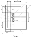
- FIGs. 4A and 4B illustrate an implementation of a patch antenna according to an aspect of the present disclosure.
- FIGs. 4A and 4B show top and cross-section side views, respectively, of a PCB 400 that provides a substrate for supporting a shorted half patch antenna according to an aspect of the present disclosure.
- the PCB 400 includes a radiating element 402 with a front edge or end 402a and a rear end or edge 402b, a grounding element 404 coupled to a ground connection 406.
- the PCB 400 also includes at least one shorting element 408 for coupling a portion of the radiating element 404 adjacent to the rear edge 402b of the radiating element 402 to the grounding element 404.
- the at least one shorting element 408 can be a plurality of vias 410 formed in the PCB 400 from conductive materials and extending vertically from the grounding element 404 up to the radiating element 402 through a dielectric material of the PCB. Further, the front edge 402a of the radiating element 402 is positioned close to an edge of the grounding element 404 but far from other edges of the grounding element 404, as discussed in further detail below.
- the PCB 400 further includes feed structure for coupling the radiating element 402 to a processing system or other component.
- the feed structure includes at least one feed line 412 and a feed via 414, where the feed line 412 is coupled to the radiating element 402 using the feed via 414.
- the feed line 412 may include at least one microstrip line in the PCB 400 and, if needed, one or more vias formed in the PCB 400 to electrically couple the feed via 414 to the processing system via the various layers of the PCB 400.
- the feed via 414 can also be a via formed in the PCB 400 and may be configured to extend vertically between the radiating element 404 and the feed line 412.
- the elements 402, 404, 406, 408, 410, 412, and 414 can be formed in a PCB using any techniques for forming vias, lines, traces, etc. in a PCB technology.
- the present disclosure contemplates the use of non-PCB technologies. In the case of non-PCB technologies, such features can be formed using corresponding techniques.
- the arrangement of the radiating element 402, the at least one shorting element 408, and the grounding element 404 are configured to provide a shorted half patch antenna.
- a patch antenna configuration has the advantage of being able to be deployed in various types of PCBs and similar technologies, such as integrated circuit packages, while the dipole antennas would require special clearance requirements.
- patch antennas can be placed directly over metal layers, solder balls or other features of the PCB.
- a patch antenna configuration also supports offers polarization diversity, which is important for the 60 GHz band, since the antennas used for 60 GHz typically have low cross polarization and the mobile side of a connection can have a random orientation.
- patch antennas can be deployed in different parts of the package to provide polarization diversity.
- an antenna In a standard patch antenna, an antenna is configured to have a radiating element coupled to a feed line and placed parallel to a grounding element.
- the standard patch antenna behaves like two slot antennas that are approximately a half wave apart. However, this also creates a two element array that has a peak gain orthogonal to the plane of the patch (i.e., at higher angles) and lower gain at the low angles, where the two slots destructively interfere. Additionally, the presence of a ground plane surrounding the patch further limits the radiation at low angles.
- a shorted half patch antenna is configured to have a radiating element coupled not only to the feed line, but also to the ground plane, which causes the half patch antenna to have only one slot. This removes the destructive interference typically encountered in a standard patch antenna at low angles. Thus, this also improves support for polarization diversity at low angles.
- a shorted half patch antenna design is characterized in that a rear edge or end of the radiating element is coupled to a grounding element and that a length of a radiating element is selected to be one quarter of a wavelength within the dielectric medium for a center frequency of operation.
- a shorted half wave patch antenna configuration is provided by configuring the radiating element 402 to have the rear edge 402b coupled to the grounding element 404 using the at least one shorting element 408.
- the shorting element 408 can be formed using a plurality of vias 410 contacting a .
- the length L of radiating element 402 is selected to be one quarter of a wavelength ( ⁇ /4) for the dielectric material constituting PCB 400 for the center frequency for a radio band of operation (e.g., 60 GHz radio band).
- the radiating element 402 is also selected to have a width W.
- the width W and the placement of feed via 414 are selected so as to provide the impedance and tuning needed for a particular application.
- radiating element 402 and grounding element 404 are illustrated herein as having rectangular shapes, this is only for ease of illustration. The present disclosure contemplates that the techniques described herein can be utilized with elements of different shapes.
- vias 410, 414, and others discussed above and below are shown as single cylindrical vias, this is solely for ease of illustration.
- the present disclosure contemplates that vias of any shape or dimensions can be used to form the half shorted patch antennas described herein.
- the shorted wall 408 can be formed using one or two wide via structures instead of the series of vias 410 illustrated in FIGs. 4A and 4B .
- the only requirement for the at least one shorting element 408 is that the shorting elements, whether vias 410 or other elements, extend along a substantial portion of the rear edge 402b. For example, at least 40%.
- the present disclosure contemplates that an improvement on standard shorted half patch antennas by careful selection of the position of the edges of the radiating element relative to the edges of the ground elements. This improvement results in enhanced forward or low angle radiation, as discussed below.
- one aspect of the shorted half patch antenna formed in PCB 400 is that the front edge 402a of the radiating element 402 is positioned close to an edge of the grounding element 404.
- one aspect of the shorted half patch antenna formed in PCB 400 is that the other edges of the radiating element 402 are positioned to be far from the edges of the grounding element 404.
- the radiating element 402 is positioned relative to the grounding element so that a lateral distance d R from the rear edge 402b to a corresponding edge of the grounding element 404 is greater than or equal to one half of the wavelength ( ⁇ /2) for the center frequency for the radio band of operation.
- the radiating element 402 is positioned relative to the grounding element 404 so that a lateral distances d 1 and d 2 from side edges 402c and 402d, respectively, of the radiating element 402 to the corresponding edges of the grounding element 404 are each greater than or equal to one half of the wavelength ( ⁇ /2) for the center frequency of operation.
- edges 402b, 402c, and 402d thus reduces the amount of attenuation for signals radiated in other directions due to the increased ground plane area for these edges versus the front edge 402a, thus favoring forward (i.e., low angle) performance.
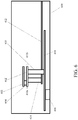
- FIG. 5 shows a PCB 500 including a shorted half patch antenna configured according to a first alternative aspect of the present disclosure.
- a PCB 500 including a shorted half patch antenna configured according to a first alternative aspect of the present disclosure.
- Such a configuration is illustrated by PCB 500 in FIG. 5 .
- this configuration results in an overall reduction of attenuation of forward (i.e., low angle) signals radiating from the radiating element 402.
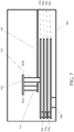
- FIG. 6 shows a PCB 600 including a patch antenna configured according to a second alternative aspect of the present disclosure.
- PCB 600 is configured substantially the same as PCB 400 in FIGs. 4A and 4B .
- PCB 600 includes a second radiating element 602 positioned above the radiating element 402 and coupled to a front end 402a of radiating element 402 using a coupling structure.
- a coupling structure For example, as shown in FIG. 6 , one or more vias 604 formed in the PCB 600 can provide such a coupling structure.
- the second radiating element 602 can be dimensioned substantially the same as radiating element 402.
- the second radiating element 602 can be positioned so that second radiating element 602 and the radiating element 402 are substantially in complete overlap with each other. This configuration results in an additional resonator being provided for the antenna. Such a configuration can be utilized to improve impedance bandwidth performance of the resulting shorted half patch antenna. In particular, this configuration can be utilized to provide a wider bandwidth.
- FIG. 7 shows a PCB 700 including a patch antenna configured according to a third alternative aspect of the present disclosure.
- PCB 700 is configured substantially the same as PCB 400 in FIGs. 4A and 4B .
- PCB 700 also includes additional grounding elements 704 1 , 704 2 , 704 3 coupled to grounding element 404 and each other using a coupling structure.
- a coupling structure may be provided in PCB 700 by vias 706 1 , 706 2 , and 706 3 .
- FIGs. 5-7 are illustrated in isolation, this is solely for ease of illustration. Rather, the present disclosure contemplates that modifications discussed above can be used in any combination with each other.
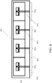
- FIG. 8 shows an array of shorted half plane antennas in accordance with an aspect of the present disclosure.
- a PCB 800 is provided showing an array 801 of antennas 802 a , 802 b , 802 c , and 802 d .
- Each of antennas 802i can be configured, for example, in accordance with any of FIGs. 4A-7 , or any variations or combinations thereof.
- the signals at each of feed lines 804 a , 804 b , 804 c , and 804 d can be adjusted in phase and/or amplitude via a control circuit (not shown) for all or each of the feed lines 804 a , 804 b , 804 c , and 804 d .
- the array 801 operates a beam former to direct signals in a particular direction.
- the coverage provided by array 801 is significantly wider than possible using standard patch antennas or even existing shorted half wave antennas.
- FIGs. 9 and 10 the performance of shorted half patch antennas according to aspects of the present disclosure is presented.
- the operation in free space for a patch antenna combining aspects of the shorted half patch antennas of FIGs. 6 and 7 was simulated. That is, a shorted half patch antenna, as described in FIGs. 4A and 4B , but with the addition of a second radiating element, as described with respect to FIG. 6 , and the addition of additional grounding elements 704 1 , 704 2 , 704 3 , as described with respect to FIG. 7 .
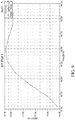
- FIG. 9 shows an X-Y plot of return loss as a function of frequency over a 60 GHz band (57.5 GHz to 66.25 GHz) for the above-described shorted half patch antenna.
- the return loss throughout the range is between -10dB and -14.5dB, meaning that less than 1/10th of the RF energy is being reflected.
- a return loss of -10dB or less is typically considered good when the devices under test are considered to be tuned and have a reasonably good impedance matching.
- FIG. 9 illustrates that the shorted half patch antenna of the present disclosure provides acceptable return loss.
- FIG. 10 shows a radiation pattern for this same shorted half patch antenna mounted on a package.
- the new shorted half patch antenna design results in substantially a same radiation pattern for high angles (+Z direction) as for low angles (+X direction). Some attenuation is observed for some high angles (-Z direction), but this is due to the package.
- FIG. 10 does show that attenuation typically observed for low angles in patch antennas is reduced or eliminated in the new shorted half patch antenna design described above.
- the various operations of methods described above may be performed by any suitable means capable of performing the corresponding functions.
- the means may include various hardware and/or software component(s) and/or module(s), including, but not limited to a circuit, an application specific integrated circuit (ASIC), or processor.
- ASIC application specific integrated circuit
- Means for generating may include a processing system, which may include one or more processors, such as the processors 210, 242, and/or the controller 230 of the access point 110 illustrated in FIG. 2 or the processor 304 and/or the DSP 320 portrayed in FIG. 3 .
- the means for outputting may comprise a transmitter (e.g., the transmitter unit 222) and/or an antenna(s) 224 of the access point 110 illustrated in FIG. 2 or the transmitter 310 and/or antenna(s) 316 depicted in FIG. 3 .
- Means for obtaining may comprise a receiver (e.g., the receiver unit 254) and/or an antenna(s) 252 of the UT 120 illustrated in FIG. 2 or the receiver 312 and/or antenna(s) 316 depicted in FIG. 3 .
- Means for determining may include a processing system, which may include one or more processors such as processors 260, 270, 288, and 290 and/or the controller 280 of the UT 120 or the processor 304 and/or the DSP 320 portrayed in FIG. 3 .
- Means for feeding may comprise the feed structure for coupling the radiating element 402 to a processing system or other component, as discussed above with respect to FIG. 4 .
- means for feeding may comprise at least one feed line 412 and a feed via 414 as discussed above with respect to FIG. 4 .
- Means for coupling the grounding element 404 to the radiating element 402 may comprise vias 410 in FIG. 4 or any combination of vias and microstrip lines in PCB 400 for coupling the grounding element 404 to the radiating element 402.
- Means for coupling the second radiating element 602 to the first radiating element 404 may comprise vias 604, as shown in FIG. 6 , or any combination of vias and microstrip lines in PCB 600.
- Means for coupling the grounding element 404 and the at least one second grounding element 706i may comprise vias 704i, as shown in FIG. 7 , or any combination of vias and microstrip lines in PCB 700.
- such means may be implemented by processing systems configured to perform the corresponding functions by implementing various algorithms (e.g., in hardware or by executing software instructions) described above.
- determining encompasses a wide variety of actions. For example, “determining” may include calculating, computing, processing, deriving, investigating, looking up (e.g., looking up in a table, a database or another data structure), ascertaining and the like. Also, “determining” may include receiving (e.g., receiving information), accessing (e.g., accessing data in a memory) and the like. Furthermore, “determining” may include resolving, selecting, choosing, establishing and the like.
- the term "outputting” may involve actual transmission or output of a structure from one entity (e.g., a processing system) to another entity (e.g., an RF front end or modem) for transmission.
- the term “obtaining” may involve actual receiving of a structure transmitted over the air or obtaining the structure by one entity (e.g., a processing system) from another entity (e.g., an RF front end or modem).
- a phrase referring to "at least one of" a list of items refers to any combination of those items, including single members.
- "at least one of: a, b, or c” is intended to cover a, b, c, a-b, a-c, b-c, and a-b-c, as well as any combination with multiples of the same element (e.g., a-a, a-a-a, a-a-b, a-a-c, a-b-b, a- c-c, b-b, b-b-b, b-b-c, c-c, and c-c-c or any other ordering of a, b, and c ).
- DSP digital signal processor
- ASIC application specific integrated circuit
- FPGA field programmable gate array
- PLD programmable logic device
- a general-purpose processor may be a microprocessor, but in the alternative, the processor may be any commercially available processor, controller, microcontroller, or state machine.
- a processor may also be implemented as a combination of computing devices, e.g., a combination of a DSP and a microprocessor, a plurality of microprocessors, one or more microprocessors in conjunction with a DSP core, or any other such configuration.
- a software module may reside in any form of storage medium that is known in the art. Some examples of storage media that may be used include random access memory (RAM), read only memory (ROM), flash memory, EPROM memory, EEPROM memory, registers, a hard disk, a removable disk, a CD-ROM and so forth.
- RAM random access memory
- ROM read only memory
- flash memory EPROM memory
- EEPROM memory EEPROM memory
- registers a hard disk, a removable disk, a CD-ROM and so forth.
- a software module may comprise a single instruction, or many instructions, and may be distributed over several different code segments, among different programs, and across multiple storage media.
- a storage medium may be coupled to a processor such that the processor can read information from, and write information to, the storage medium. In the alternative, the storage medium may be integral to the processor.
- the methods disclosed herein comprise one or more steps or actions for achieving the described method.
- the method steps and/or actions may be interchanged with one another without departing from the scope of the claims.
- the order and/or use of specific steps and/or actions may be modified without departing from the scope of the claims.
- an example hardware configuration may comprise a processing system in a wireless node.
- the processing system may be implemented with a bus architecture.
- the bus may include any number of interconnecting buses and bridges depending on the specific application of the processing system and the overall design constraints.
- the bus may link together various circuits including a processor, machine-readable media, and a bus interface.
- the bus interface may be used to couple a network adapter, among other things, to the processing system via the bus.
- the network adapter may be used to implement the signal processing functions of the Physical (PHY) layer.
- PHY Physical
- a user interface e.g., keypad, display, mouse, joystick, etc.
- the bus may also link various other circuits such as timing sources, peripherals, voltage regulators, power management circuits, and the like, which are well known in the art, and therefore, will not be described any further.
- the processor may be responsible for managing the bus and general processing, including the execution of software stored on the machine-readable media.
- the processor may be implemented with one or more general-purpose and/or special-purpose processors. Examples include microprocessors, microcontrollers, DSP processors, and other circuitry that can execute software.
- Software shall be construed broadly to mean instructions, data, or any combination thereof, whether referred to as software, firmware, middleware, microcode, hardware description language, or otherwise.
- Machine-readable media may include, by way of example, RAM (Random Access Memory), flash memory, ROM (Read Only Memory), PROM (Programmable Read-Only Memory), EPROM (Erasable Programmable Read-Only Memory), EEPROM (Electrically Erasable Programmable Read-Only Memory), registers, magnetic disks, optical disks, hard drives, or any other suitable storage medium, or any combination thereof.
- the machine-readable media may comprise a computer-readable medium having instructions stored (and/or encoded) thereon, the instructions being executable by one or more processors to perform the operations described herein and be embodied in a computer-program product.
- the computer-program product may comprise packaging materials to advertise the computer-readable medium therein for purchase by consumers.
- the machine-readable media may be part of the processing system separate from the processor.
- the machine-readable media, or any portion thereof may be external to the processing system.
- the machine-readable media may include a transmission line, a carrier wave modulated by data, and/or a computer readable storage medium with instructions stored thereon separate from the wireless node, all of which may be accessed by the processor through the bus interface.
- the machine-readable media, or any portion thereof may be integrated into the processor, such as the case may be with cache and/or general register files.
- the processing system may be configured as a general-purpose processing system with one or more microprocessors providing the processor functionality and external memory providing at least a portion of the machine-readable media, all linked together with other supporting circuitry through an external bus architecture.
- the processing system may be implemented with an ASIC (Application Specific Integrated Circuit) with the processor, the bus interface, the user interface in the case of an access terminal), supporting circuitry, and at least a portion of the machine-readable media integrated into a single chip, or with one or more FPGAs (Field Programmable Gate Arrays), PLDs (Programmable Logic Devices), controllers, state machines, gated logic, discrete hardware components, or any other suitable circuitry, or any combination of circuits that can perform the various functionality described throughout this disclosure.
- FPGAs Field Programmable Gate Arrays
- PLDs Programmable Logic Devices
- controllers state machines, gated logic, discrete hardware components, or any other suitable circuitry, or any combination of circuits that can perform the various functionality described throughout this disclosure.
- the machine-readable media may comprise a number of software modules.
- the software modules include instructions that, when executed by an apparatus such as a processor, cause the processing system to perform various functions.
- the software modules may include a transmission module and a receiving module.
- Each software module may reside in a single storage device or be distributed across multiple storage devices.
- a software module may be loaded into RAM from a hard drive when a triggering event occurs.
- the processor may load some of the instructions into cache to increase access speed.
- One or more cache lines may then be loaded into a general register file for execution by the processor.
- Computer-readable media include both computer storage media and communication media including any medium that facilitates transfer of a computer program from one place to another.
- a storage medium may be any available medium that can be accessed by a computer.
- such computer-readable media can comprise RAM, ROM, EEPROM, CD-ROM or other optical disk storage, magnetic disk storage or other magnetic storage devices, or any other medium that can be used to carry or store desired program code in the form of instructions or data structures and that can be accessed by a computer.
- any connection is properly termed a computer-readable medium.
- Disk and disc include compact disc (CD), laser disc, optical disc, digital versatile disc (DVD), floppy disk, and Blu-ray® disc where disks usually reproduce data magnetically, while discs reproduce data optically with lasers.
- computer-readable media may comprise non-transitory computer-readable media (e.g., tangible media).
- computer-readable media may comprise transitory computer- readable media (e.g., a signal). Combinations of the above should also be included within the scope of computer-readable media.
- modules and/or other appropriate means for performing the methods and techniques described herein can be downloaded and/or otherwise obtained by a user terminal and/or base station as applicable.
- a user terminal and/or base station can be coupled to a server to facilitate the transfer of means for performing the methods described herein.
- various methods described herein can be provided via storage means (e.g., RAM, ROM, a physical storage medium such as a compact disc (CD) or floppy disk, etc.), such that a user terminal and/or base station can obtain the various methods upon coupling or providing the storage means to the device.
- storage means e.g., RAM, ROM, a physical storage medium such as a compact disc (CD) or floppy disk, etc.
- CD compact disc
- floppy disk etc.
- any other suitable technique for providing the methods and techniques described herein to a device can be utilized.
Description
- Aspects of the present disclosure relate generally to patch antenna circuits for communications devices, and more particularly, to shorted half patch antenna designs for enhanced low angle radiation performance.
- Communications using the 60 GHz band are of particular interest for providing short-range, high throughput data links for electronic consumer devices. To support such communications in many types of electronic consumer devices, low profile and low area antennas are required that can radiate is all possible directions, including forward or low angle directions. One method for providing antennas in consumer devices to support low angle radiation is using a printed dipole antenna on the edge of a printed circuit board (PCB). This method creates radiation that is polarized parallel to the PCB it is printed on. However, this approach has drawbacks due to the nature of dipole antennas. In particular, a dipole antenna behaves like a resonant circuit that has a series inductor and shunt capacitor. Therefore, if there are too many other conductive elements on the PCB in the vicinity of the dipole, the capacitance may become too large and the bandwidth of the antenna can suffer. Moreover, reducing the number of such other conductive elements in the vicinity of the dipole antenna is difficult, as modern PCB designs typically require a high circuit density for costs and/or size purposes. Therefore, keeping the necessary clearances for the dipole antenna to work properly is difficult. Another method for providing low angle radiation antennas in PCBs are closed cavity backed slot antennas. However, while closed cavity backed slot antennas are less sensitive to proximity issues than dipole antennas, the presence of the cavity makes closed cavity backed slot antennas more difficult to tune over the bandwidth required for 60 GHZ (14%).
- HE J-W ET AL, "Design considerations of planar inverted-F antenna (PIFA) on a finite ground plane", THE 2004 JOINT CONFERENCE OF THE 10TH ASIA-PACIFIC CONFERENCE ON COMMUNICATIONS AND THE 5TH INTERNATIONAL SYMPOSIUM ON MULTI-DIMENSIONAL MOBILE COMMUNICATIONS PROCEEDINGS, BEIJING, CHINA 29 AUG.-1 SEPT. 2004, PISCATAWAY, NJ, USA, IEEE, US, (20040829), vol. 2, doi:10.1109/APCC.2004.1391797, ISBN 978-0-7803-8601-3 concerns the operation of a PIFA mounted on a finite ground plane. This includes the influence on the input and radiation characteristics caused by the placements of the short-circuit plate and the feed wire as well as where the antenna is mounted on a finite ground plane. It has been found that the location where the antenna is mounted on the finite ground plane has a significant impact on the resonant frequency, bandwidth and radiation characteristics.
-
US 2012/299778 A1 concerns an antenna that includes a substrate and a top plate disposed over the substrate. At least one feed line is connected to the top plate, and each feed line comprises a first through-silicon via (TSV) structure passing through the substrate. -
US 2007/057847 A1 concerns an antenna that includes a first radiating element, a feeding point, a grounding point, a second radiating element, and first and second conductive elements. The first radiating element has opposite first and second sides. The feeding point is provided on the first radiating element, and is disposed adjacent to the first side of the first radiating element. -
US 2012/212384 A1 concerns a chip package that includes a plurality of layers including conductive planes connected by vias. The layers include a first portion having an antenna formed therein and a parallel-plate mode suppression mechanism to suppress parallel-plate mode excitation of the antenna. -
US 2002/041256 A1 relates to an antenna apparatus and a portable wireless communication apparatus. - The following presents a simplified summary of one or more embodiments in order to provide a basic understanding of such embodiments. This summary is not an extensive overview of all contemplated embodiments, and is intended to neither identify key or critical elements of all embodiments nor delineate the scope of any or all embodiments. Its sole purpose is to present some concepts of one or more embodiments in a simplified form as a prelude to the more detailed description that is presented later.
- An aspect of the present disclosure involves an apparatus for wireless communications. The apparatus includes a grounding element, a radiating element above the grounding element and having opposing front and rear edges, and at least one shorting element coupling the grounding element to a portion of the radiating element adjacent to the rear edge of the radiating element. In the apparatus, a length of the radiating element from the front edge to the rear edge is equal to approximately one quarter of a wavelength for a frequency within a radio band for operating the apparatus, a lateral distance from the front edge of the radiating element to a corresponding edge of the grounding element are less than or equal to approximately one half of the wavelength, and a lateral distance from the rear edge of the radiating element to a corresponding edge of the grounding element is greater than or equal to approximately one half of the wavelength.
- Another aspect of the present disclosure involves an apparatus for wireless communications. The apparatus includes a grounding element, a radiating element above the grounding element and having opposing front and rear edges, means for coupling the grounding element to a portion of the radiating element adjacent to the rear edge of the radiating element, and means for feeding the radiating element. In the apparatus, a length of the radiating element from the front edge to the rear edge is equal to approximately one quarter of a wavelength for a frequency within a radio band for operating the apparatus, a lateral distance from the front edge of the radiating element to a corresponding edge of the grounding element are less than or equal to approximately one half of the wavelength, and a lateral distance from the rear edge of the radiating element to a corresponding edge of the grounding element is greater than or equal to approximately one half of the wavelength.
- Another aspect of the present disclosure involves a method of manufacturing an apparatus for wireless communication. The method includes providing a substrate, forming a grounding element on the substrate, forming a radiating element above the grounding element with opposing front and rear edges, and coupling the grounding element to a portion of the radiating element adjacent to the rear edge of the radiating element via at least one shorting element. In the method, a length of the radiating element from the front edge to the rear edge is selected to be equal to approximately one quarter of a wavelength for a frequency within a radio band for operating the apparatus, a lateral distance from the front edge of the radiating element to a corresponding edge of the grounding element is selected to be less than or equal to approximately one half of the wavelength, and a lateral distance from the rear edge of the radiating element to a corresponding edge of the grounding element is selected to be greater than or equal to approximately one half of the wavelength.
- Another aspect of the present disclosure involves a wireless station. The wireless station includes at least one antenna having a grounding element, a radiating element above the grounding element and having opposing front and rear edges, and at least one shorting element coupling the grounding element to a portion of the radiating element adjacent to the rear edge of the radiating element. The wireless station also includes a receiver configured to receive, via the at least one antenna, signals transmitted in a network and a processing system configured to determine, based on the signals, information transmitted in the network. In the wireless station, a length of the radiating element from the front edge to the rear edge is equal to approximately one quarter of a wavelength for a frequency within a radio band for operating the apparatus, a lateral distance from the front edge of the radiating element to a corresponding edge of the grounding element are less than or equal to approximately one half of the wavelength, and a lateral distance from the rear edge of the radiating element to a corresponding edge of the grounding element is greater than or equal to approximately one half of the wavelength.
- Another aspect of the present disclosure involves an access point. The access point includes at least one antenna having a grounding element, a radiating element above the grounding element and having opposing front and rear edges, and at least one shorting element coupling the grounding element to a portion of the radiating element adjacent to the rear edge of the radiating element. The access point also includes a processing system configured to generate signals corresponding to information for transmission in a network and a transmitter configured to transmit, via the at least one antenna, the signals for transmission in the network. In the access point, a length of the radiating element from the front edge to the rear edge is equal to approximately one quarter of a wavelength for a frequency within a radio band for operating the apparatus, a lateral distance from the front edge of the radiating element to a corresponding edge of the grounding element are less than or equal to approximately one half of the wavelength, and a lateral distance from the rear edge of the radiating element to a corresponding edge of the grounding element is greater than or equal to approximately one half of the wavelength.
- To the accomplishment of the foregoing and related ends, the one or more embodiments comprise the features hereinafter fully described and particularly pointed out in the claims. The following description and the annexed drawings set forth in detail certain illustrative aspects of the one or more embodiments. These aspects are indicative, however, of but a few of the various ways in which the principles of various embodiments may be employed and the described embodiments are intended to include all such aspects. The scope of the invention is defined by the claims. If an example does not fall under the scope defined by the claims, it is to be understood as illustrative for a better understanding of the invention.
-
-
FIG. 1 illustrates a diagram of an example wireless communications network, in accordance with certain aspects of the present disclosure. -
FIG. 2 illustrates a block diagram of an example access point and user terminals, in accordance with certain aspects of the present disclosure. -
FIG. 3 illustrates a block diagram of an example wireless device, in accordance with certain aspects of the present disclosure. -
FIGs. 4A and4B shows top and cross-section side views, respectively, of a PCB including patch antenna according to an aspect of the present disclosure. -
FIG. 5 shows a PCB including a patch antenna configured according to a first alternative aspect of the present disclosure. -
FIG. 6 shows a PCB including a patch antenna configured according to a first alternative aspect of the present disclosure. -
FIG. 7 shows a PCB including a patch antenna configured according to a first alternative aspect of the present disclosure. -
FIG. 8 shows a PCB including an array of patch antennas configured according to an aspect of the present disclosure. -
FIG. 9 shows an X-Y plot of return loss over a 60 GHz band for a patch antenna according to an aspect of the present disclosure. -
FIG. 10 shows a radiation pattern for a patch antenna according to an aspect of the present disclosure. - Various aspects of the disclosure are described more fully hereinafter with reference to the accompanying drawings. This disclosure may, however, be embodied in many different forms and should not be construed as limited to any specific structure or function presented throughout this disclosure. Rather, these aspects are provided so that this disclosure will be thorough and complete, and will fully convey the scope of the disclosure to those skilled in the art. Based on the teachings herein one skilled in the art should appreciate that the scope of the disclosure is intended to cover any aspect of the disclosure disclosed herein, whether implemented independently of or combined with any other aspect of the disclosure. For example, an apparatus may be implemented or a method may be practiced using any number of the aspects set forth herein. In addition, the scope of the disclosure is intended to cover such an apparatus or method which is practiced using other structure, functionality, or structure and functionality in addition to or other than the various aspects of the disclosure set forth herein. It should be understood that any aspect of the disclosure disclosed herein may be embodied by one or more elements of a claim.
- The present disclosure is related to an antenna array design for Access Point (AP) devices and other similar devices, as shown below. For convenience, this improved patch antenna design will be described in the context of an AP device implementation of this antenna design. However, it is understood that techniques described herein may have other applications, as will be explained further below.
- Although particular aspects are described herein, many variations and permutations of these aspects fall within the scope of the disclosure. Although some benefits and advantages of the preferred aspects are mentioned, the scope of the disclosure is not intended to be limited to particular benefits, uses, or objectives. Rather, aspects of the disclosure are intended to be broadly applicable to different wireless technologies, system configurations, networks, and transmission protocols, some of which are illustrated by way of example in the figures and in the following description of the preferred aspects. The detailed description and drawings are merely illustrative of the disclosure rather than limiting and the scope of the disclosure is being defined by the appended claims.
- The teachings herein may be incorporated into (e.g., implemented within or performed by) a variety of wired or wireless apparatuses (e.g., nodes). In some aspects, a wireless node implemented in accordance with the teachings herein may comprise an access point or an access terminal. A wireless node may provide, for example, connectivity for or to a network (e.g., a wide area network such as the Internet or a cellular network) via a wired or wireless communication link.
- An access point ("AP") may comprise, be implemented as, or known as a Node B, Radio Network Controller ("RNC"), evolved Node B (eNB), Base Station Controller ("BSC"), Base Transceiver Station ("BTS"), Base Station ("BS"), Transceiver Function ("TF"), Radio Router, Radio Transceiver, Basic Service Set ("BSS"), Extended Service Set ("ESS"), Radio Base Station ("RBS"), or some other terminology.
- An access terminal ("AT") may comprise, be implemented as, or known as a subscriber station, a subscriber unit, a mobile station (MS), a remote station, a remote terminal, a user terminal (UT), a user agent, a user device, user equipment (UE), a user station, or some other terminology. In some implementations, an access terminal may comprise a cellular telephone, a cordless telephone, a Session Initiation Protocol ("SIP") phone, a wireless local loop ("WLL") station, a personal digital assistant ("PDA"), a handheld device having wireless connection capability, a Station ("STA"), or some other suitable processing device coupled to a wireless modem. Accordingly, one or more aspects taught herein may be incorporated into a phone (e.g., a cellular phone or smart phone), a computer (e.g., a laptop), a tablet, a portable communication device, a portable computing device (e.g., a personal data assistant), an entertainment device (e.g., a music or video device, or a satellite radio), a global positioning system (GPS) device, or any other suitable device that is configured to communicate via a wireless or wired medium.
- The techniques described herein may be used for various broadband wireless communication systems, including communication systems that are based on an orthogonal multiplexing scheme. Examples of such communication systems include Spatial Division Multiple Access (SDMA) system, Time Division Multiple Access (TDMA) system, Orthogonal Frequency Division Multiple Access (OFDMA) system and Single-Carrier Frequency Division Multiple Access (SC-FDMA) systems. An SDMA system may utilize sufficiently different directions to simultaneously transmit data belonging to multiple user terminals. A TDMA system may allow multiple user terminals to share the same frequency channel by dividing the transmission signal into different time slots, each time slot being assigned to different user terminal. An OFDMA system utilizes orthogonal frequency division multiplexing (OFDM), which is a modulation technique that partitions the overall system bandwidth into multiple orthogonal sub-carriers. These sub-carriers may also be called tones, bins, etc. With OFDM, each sub-carrier may be independently modulated with data. An SC-FDMA system may utilize interleaved FDMA (IFDMA) to transmit on sub-carriers that are distributed across the system bandwidth, localized FDMA (LFDMA) to transmit on a block of adjacent sub-carriers, or enhanced FDMA (EFDMA) to transmit on multiple blocks of adjacent sub-carriers. In general, modulation symbols are sent in the frequency domain with OFDM and in the time domain with SC-FDMA.
- The teachings herein may be incorporated into (e.g., implemented within or performed by) a variety of wired or wireless apparatuses (e.g., nodes). In some aspects, a wireless node implemented in accordance with the teachings herein may comprise an access point or an access terminal. A wireless node may provide, for example, connectivity for or to a network (e.g., a wide area network such as the Internet or a cellular network) via a wired or wireless communication link.
- An access point ("AP") may comprise, be implemented as, or known as a Node B, Radio Network Controller ("RNC"), evolved Node B (eNB), Base Station Controller ("BSC"), Base Transceiver Station ("BTS"), Base Station ("BS"), Transceiver Function ("TF"), Radio Router, Radio Transceiver, Basic Service Set ("BSS"), Extended Service Set ("ESS"), Radio Base Station ("RBS"), or some other terminology.
- An access terminal ("AT") may comprise, be implemented as, or known as a subscriber station, a subscriber unit, a mobile station (MS), a remote station, a remote terminal, a user terminal (UT), a user agent, a user device, user equipment (UE), a user station, or some other terminology. In some implementations, an access terminal may comprise a cellular telephone, a cordless telephone, a Session Initiation Protocol ("SIP") phone, a wireless local loop ("WLL") station, a personal digital assistant ("PDA"), a handheld device having wireless connection capability, a Station ("STA"), or some other suitable processing device coupled to a wireless modem. Accordingly, one or more aspects taught herein may be incorporated into a phone (e.g., a cellular phone or smart phone), a computer (e.g., a laptop), a tablet, a portable communication device, a portable computing device (e.g., a personal data assistant), an entertainment device (e.g., a music or video device, or a satellite radio), a global positioning system (GPS) device, or any other suitable device that is configured to communicate via a wireless or wired medium.
-
FIG. 1 illustrates an example wireless communication system in which aspects of the present disclosure may be practiced. For example,AP 110 may be configured to generate and transmit a frame having one or more bits that indicate both minimum and maximum bandwidths for communicating in a network. UT 120 may be configured to obtain (e.g., receive) the frame and determine, based on the one or more bits in the frame, both the minimum and maximum bandwidths for communicating in the network. -
FIG. 1 illustrates a multiple-access multiple-input multiple-output (MIMO)system 100 with access points and user terminals. For simplicity, only oneaccess point 110 is shown inFIG. 1 . An access point is generally a fixed station that communicates with the user terminals and may also be referred to as a base station or some other terminology. A user terminal may be fixed or mobile and may also be referred to as a mobile station, a wireless device, a user equipment, or some other terminology.Access point 110 may communicate with one or more user terminals 120 at any given moment on the downlink and uplink. The downlink (i.e., forward link) is the communication link from the access point to the user terminals, and the uplink (i.e., reverse link) is the communication link from the user terminals to the access point. A user terminal may also communicate peer-to-peer with another user terminal. - A
system controller 130 may provide coordination and control for these APs and/or other systems. The APs may be managed by thesystem controller 130, for example, which may handle adjustments to radio frequency power, channels, authentication, and security. Thesystem controller 130 may communicate with the APs via a backhaul. The APs may also communicate with one another, e.g., directly or indirectly via a wireless or wireline backhaul. - While portions of the following disclosure will describe user terminals 120 capable of communicating via Spatial Division Multiple Access (SDMA), for certain aspects, the user terminals 120 may also include some user terminals that do not support SDMA. Thus, for such aspects, an
AP 110 may be configured to communicate with both SDMA and non-SDMA user terminals. This approach may conveniently allow older versions of user terminals ("legacy" stations) to remain deployed in an enterprise, extending their useful lifetime, while allowing newer SDMA user terminals to be introduced as deemed appropriate. - The
system 100 employs multiple transmit and multiple receive antennas for data transmission on the downlink and uplink. Theaccess point 110 is equipped with Nap antennas and represents the multiple-input (MI) for downlink transmissions and the multiple-output (MO) for uplink transmissions. A set of K selected user terminals 120 collectively represents the multiple-output for downlink transmissions and the multiple-input for uplink transmissions. For pure SDMA, it is desired to have Nap ≥ K ≥ 1 if the data symbol streams for the K user terminals are not multiplexed in code, frequency or time by some means. K may be greater than Nap if the data symbol streams can be multiplexed using TDMA technique, different code channels with CDMA, disjoint sets of subbands with OFDM, and so on. Each selected user terminal transmits user-specific data to and/or receives user-specific data from the access point. In general, each selected user terminal may be equipped with one or multiple antennas (i.e., Nut ≥ 1). The K selected user terminals can have the same or different number of antennas. - The SDMA system may be a time division duplex (TDD) system or a frequency division duplex (FDD) system. For a TDD system, the downlink and uplink share the same frequency band. For an FDD system, the downlink and uplink use different frequency bands.
MIMO system 100 may also utilize a single carrier or multiple carriers for transmission. Each user terminal may be equipped with a single antenna (e.g., in order to keep costs down) or multiple antennas (e.g., where the additional cost can be supported). Thesystem 100 may also be a TDMA system if the user terminals 120 share the same frequency channel by dividing transmission/reception into different time slots, each time slot being assigned to different user terminal 120. -
FIG. 2 illustrates example components of theAP 110 and UT 120 illustrated inFIG. 1 , which may be used to implement aspects of the present disclosure. One or more components of theAP 110 and UT 120 may be used to practice aspects of the present disclosure. For example, antenna 224, Tx/Rx 222,processors controller 230 may be used to perform the operations described herein. Similarly, antenna 252, Tx/Rx 254, processors 260, 270, 288, and 290, and/or controller 280 may be used to perform the operations described herein. -
FIG. 2 illustrates a block diagram ofaccess point 110 and two user terminals 120m and 120x inMIMO system 100. Theaccess point 110 is equipped with Nt antennas 224a through 224ap. User terminal 120m is equipped with Nut,m antennas 252ma through 252mu, and user terminal 120x is equipped with Nut,x antennas 252xa through 252xu. Theaccess point 110 is a transmitting entity for the downlink and a receiving entity for the uplink. Each user terminal 120 is a transmitting entity for the uplink and a receiving entity for the downlink. As used herein, a "transmitting entity" is an independently operated apparatus or device capable of transmitting data via a wireless channel, and a "receiving entity" is an independently operated apparatus or device capable of receiving data via a wireless channel. In the following description, the subscript "dn" denotes the downlink, the subscript "up" denotes the uplink, Nup user terminals are selected for simultaneous transmission on the uplink, Ndn user terminals are selected for simultaneous transmission on the downlink, Nup may or may not be equal to Ndn, and Nup and Ndn may be static values or can change for each scheduling interval. The beam-steering or some other spatial processing technique may be used at the access point and user terminal. - On the uplink, at each user terminal 120 selected for uplink transmission, a transmit (TX) data processor 288 receives traffic data from a data source 286 and control data from a controller 280. The controller 280 may be coupled with a
memory 282. TX data processor 288 processes (e.g., encodes, interleaves, and modulates) the traffic data for the user terminal based on the coding and modulation schemes associated with the rate selected for the user terminal and provides a data symbol stream. A TX spatial processor 290 performs spatial processing on the data symbol stream and provides Nut,m transmit symbol streams for the Nut,m antennas. Each transmitter unit (TMTR) 254 receives and processes (e.g., converts to analog, amplifies, filters, and frequency upconverts) a respective transmit symbol stream to generate an uplink signal. Nut,m transmitter units 254 provide Nut,m uplink signals for transmission from Nut,m antennas 252 to the access point. - Nup user terminals may be scheduled for simultaneous transmission on the uplink. Each of these user terminals performs spatial processing on its data symbol stream and transmits its set of transmit symbol streams on the uplink to the access point.
- At
access point 110, Nap antennas 224a through 224ap receive the uplink signals from all Nup user terminals transmitting on the uplink. Each antenna 224 provides a received signal to a respective receiver unit (RCVR) 222. Each receiver unit 222 performs processing complementary to that performed by transmitter unit 254 and provides a received symbol stream. An RXspatial processor 240 performs receiver spatial processing on the Nap received symbol streams from Nap receiver units 222 and provides Nup recovered uplink data symbol streams. The receiver spatial processing is performed in accordance with the channel correlation matrix inversion (CCMI), minimum mean square error (MMSE), soft interference cancellation (SIC), or some other technique. Each recovered uplink data symbol stream is an estimate of a data symbol stream transmitted by a respective user terminal. AnRX data processor 242 processes (e.g., demodulates, deinterleaves, and decodes) each recovered uplink data symbol stream in accordance with the rate used for that stream to obtain decoded data. The decoded data for each user terminal may be provided to adata sink 244 for storage and/or acontroller 230 for further processing. Thecontroller 230 may be coupled with amemory 232. - On the downlink, at
access point 110, aTX data processor 210 receives traffic data from adata source 208 for Ndn user terminals scheduled for downlink transmission, control data from acontroller 230, and possibly other data from ascheduler 234. The various types of data may be sent on different transport channels.TX data processor 210 processes (e.g., encodes, interleaves, and modulates) the traffic data for each user terminal based on the rate selected for that user terminal.TX data processor 210 provides Ndn downlink data symbol streams for the Ndn user terminals. A TXspatial processor 220 performs spatial processing (such as a precoding or beamforming, as described in the present disclosure) on the Ndn downlink data symbol streams, and provides Nap transmit symbol streams for the Nap antennas. Each transmitter unit 222 receives and processes a respective transmit symbol stream to generate a downlink signal. Nap transmitter units 222 providing Nap downlink signals for transmission from Nap antennas 224 to the user terminals. - At each user terminal 120, Nut,m antennas 252 receive the Nap downlink signals from
access point 110. Each receiver unit 254 processes a received signal from an associated antenna 252 and provides a received symbol stream. An RX spatial processor 260 performs receiver spatial processing on Nut,m received symbol streams from Nut,m receiver units 254 and provides a recovered downlink data symbol stream for the user terminal. The receiver spatial processing is performed in accordance with the CCMI, MMSE or some other technique. An RX data processor 270 processes (e.g., demodulates, deinterleaves and decodes) the recovered downlink data symbol stream to obtain decoded data for the user terminal. The decoded data for each user terminal may be provided to a data sink 272 for storage and/or a controller 280 for further processing. - At each user terminal 120, a channel estimator 278 estimates the downlink channel response and provides downlink channel estimates, which may include channel gain estimates, SNR estimates, noise variance and so on. Similarly, at
access point 110, achannel estimator 228 estimates the uplink channel response and provides uplink channel estimates. Controller 280 for each user terminal typically derives the spatial filter matrix for the user terminal based on the downlink channel response matrix Hdn,m for that user terminal.Controller 230 derives the spatial filter matrix for the access point based on the effective uplink channel response matrix Hup,eff . Controller 280 for each user terminal may send feedback information (e.g., the downlink and/or uplink eigenvectors, eigenvalues, SNR estimates, and so on) to the access point.Controllers 230 and 280 also control the operation of various processing units ataccess point 110 and user terminal 120, respectively. -
FIG. 3 illustrates example components that may be utilized in theAP 110 and/or UT 120 to implement aspects of the present disclosure. For example, thetransmitter 310, antenna(s) 316,processor 304 and/or theDSP 320 may be used to practice aspects of the present disclosure implemented by the AP. Further, thereceiver 312, antenna(s) 316,processor 304 and/or theDSP 320 may be used to practice aspects of the present disclosure implemented by the UT. -
FIG. 3 illustrates various components that may be utilized in awireless device 302 that may be employed within theMIMO system 100. Thewireless device 302 is an example of a device that may be configured to implement the various methods described herein. Thewireless device 302 may be anaccess point 110 or a user terminal 120. - The
wireless device 302 may include aprocessor 304 which controls operation of thewireless device 302. Theprocessor 304 may also be referred to as a central processing unit (CPU).Memory 306, which may include both read-only memory (ROM) and random access memory (RAM), provides instructions and data to theprocessor 304. A portion of thememory 306 may also include non-volatile random access memory (NVRAM). Theprocessor 304 typically performs logical and arithmetic operations based on program instructions stored within thememory 306. The instructions in thememory 306 may be executable to implement the methods described herein. - The
wireless device 302 may also include a housing 308 that may include atransmitter 310 and areceiver 312 to allow transmission and reception of data between thewireless device 302 and a remote node. Thetransmitter 310 andreceiver 312 may be combined into atransceiver 314. A single or a plurality of transmitantennas 316 may be attached to the housing 308 and electrically coupled to thetransceiver 314. Thewireless device 302 may also include (not shown) multiple transmitters, multiple receivers, and multiple transceivers. - The
wireless device 302 may also include asignal detector 318 that may be used in an effort to detect and quantify the level of signals received by thetransceiver 314. Thesignal detector 318 may detect such signals as total energy, energy per subcarrier per symbol, power spectral density and other signals. Thewireless device 302 may also include a digital signal processor (DSP) 320 for use in processing signals. - The various components of the
wireless device 302 may be coupled together by abus system 322, which may include a power bus, a control signal bus, and a status signal bus in addition to a data bus. - To provide a better foundation for understanding the various aspects of the present disclosure, reference is now made to
FIGs. 4A and4B which illustrate an implementation of a patch antenna according to an aspect of the present disclosure. -
FIGs. 4A and4B , show top and cross-section side views, respectively, of aPCB 400 that provides a substrate for supporting a shorted half patch antenna according to an aspect of the present disclosure. As shown inFIGs. 4A and4B , thePCB 400 includes aradiating element 402 with a front edge or end 402a and a rear end oredge 402b, agrounding element 404 coupled to aground connection 406. ThePCB 400 also includes at least one shortingelement 408 for coupling a portion of the radiatingelement 404 adjacent to therear edge 402b of the radiatingelement 402 to thegrounding element 404. For example, in some aspects, the at least one shortingelement 408 can be a plurality ofvias 410 formed in thePCB 400 from conductive materials and extending vertically from thegrounding element 404 up to theradiating element 402 through a dielectric material of the PCB. Further, thefront edge 402a of the radiatingelement 402 is positioned close to an edge of thegrounding element 404 but far from other edges of thegrounding element 404, as discussed in further detail below. - The
PCB 400 further includes feed structure for coupling theradiating element 402 to a processing system or other component. In particular, the feed structure includes at least onefeed line 412 and a feed via 414, where thefeed line 412 is coupled to theradiating element 402 using the feed via 414. For example, in some aspects, thefeed line 412 may include at least one microstrip line in thePCB 400 and, if needed, one or more vias formed in thePCB 400 to electrically couple the feed via 414 to the processing system via the various layers of thePCB 400. The feed via 414 can also be a via formed in thePCB 400 and may be configured to extend vertically between the radiatingelement 404 and thefeed line 412. - The
elements - In
PCB 400, the arrangement of the radiatingelement 402, the at least one shortingelement 408, and thegrounding element 404 are configured to provide a shorted half patch antenna. A patch antenna configuration has the advantage of being able to be deployed in various types of PCBs and similar technologies, such as integrated circuit packages, while the dipole antennas would require special clearance requirements. For example, patch antennas can be placed directly over metal layers, solder balls or other features of the PCB. Second, a patch antenna configuration also supports offers polarization diversity, which is important for the 60 GHz band, since the antennas used for 60 GHz typically have low cross polarization and the mobile side of a connection can have a random orientation. Thus, patch antennas can be deployed in different parts of the package to provide polarization diversity. - In a standard patch antenna, an antenna is configured to have a radiating element coupled to a feed line and placed parallel to a grounding element. In this configuration, the standard patch antenna behaves like two slot antennas that are approximately a half wave apart. However, this also creates a two element array that has a peak gain orthogonal to the plane of the patch (i.e., at higher angles) and lower gain at the low angles, where the two slots destructively interfere. Additionally, the presence of a ground plane surrounding the patch further limits the radiation at low angles. In contrast, a shorted half patch antenna is configured to have a radiating element coupled not only to the feed line, but also to the ground plane, which causes the half patch antenna to have only one slot. This removes the destructive interference typically encountered in a standard patch antenna at low angles. Thus, this also improves support for polarization diversity at low angles.
- A shorted half patch antenna design is characterized in that a rear edge or end of the radiating element is coupled to a grounding element and that a length of a radiating element is selected to be one quarter of a wavelength within the dielectric medium for a center frequency of operation. In
PCB 400, a shorted half wave patch antenna configuration is provided by configuring the radiatingelement 402 to have therear edge 402b coupled to thegrounding element 404 using the at least one shortingelement 408. The shortingelement 408 can be formed using a plurality ofvias 410 contacting a . Further, the length L of radiatingelement 402 is selected to be one quarter of a wavelength (λ/4) for the dielectricmaterial constituting PCB 400 for the center frequency for a radio band of operation (e.g., 60 GHz radio band). The radiatingelement 402 is also selected to have a width W. The width W and the placement of feed via 414 are selected so as to provide the impedance and tuning needed for a particular application. - Although radiating
element 402 andgrounding element 404 are illustrated herein as having rectangular shapes, this is only for ease of illustration. The present disclosure contemplates that the techniques described herein can be utilized with elements of different shapes. - Further, although
vias wall 408 can be formed using one or two wide via structures instead of the series ofvias 410 illustrated inFIGs. 4A and4B . Thus, the only requirement for the at least one shortingelement 408 is that the shorting elements, whethervias 410 or other elements, extend along a substantial portion of therear edge 402b. For example, at least 40%. - The present disclosure contemplates that an improvement on standard shorted half patch antennas by careful selection of the position of the edges of the radiating element relative to the edges of the ground elements. This improvement results in enhanced forward or low angle radiation, as discussed below.
- As noted above, one aspect of the shorted half patch antenna formed in
PCB 400 is that thefront edge 402a of the radiatingelement 402 is positioned close to an edge of thegrounding element 404. In particular, the radiatingelement 402 is positioned relative to the grounding element so that a lateral distance dF from thefront edge 402a to a corresponding edge of thegrounding element 404 is less than or equal to one half of the wavelength (λ/2) for the center frequency for the radio band of operation. In particular implementations, this distance can be zero (dF = 0). Placing the radiatingelement 402 with respect to thegrounding element 404 in this manner thus reduces that the amount of ground plane that would attenuate the forward direction, low angle radiated signals. In some implementations, this effect can be further improved by placing the forward edge102a as close as possible to an outer edge of thePCB 400 itself, i.e., reduce dF_PCB as much as possible. In particular implementations, this distance can be zero (dF_PCB = 0). - As further noted above, one aspect of the shorted half patch antenna formed in
PCB 400 is that the other edges of the radiatingelement 402 are positioned to be far from the edges of thegrounding element 404. In particular, the radiatingelement 402 is positioned relative to the grounding element so that a lateral distance dR from therear edge 402b to a corresponding edge of thegrounding element 404 is greater than or equal to one half of the wavelength (λ/2) for the center frequency for the radio band of operation. Similarly, the radiatingelement 402 is positioned relative to thegrounding element 404 so that a lateral distances d1 and d2 fromside edges element 402 to the corresponding edges of thegrounding element 404 are each greater than or equal to one half of the wavelength (λ/2) for the center frequency of operation. Such a configuration foredges front edge 402a, thus favoring forward (i.e., low angle) performance. - The configuration of
FIGs. 4A and4B can be modified in a variety of ways to further improve performance. One such modification is illustrated inFIG. 5 , which shows aPCB 500 including a shorted half patch antenna configured according to a first alternative aspect of the present disclosure. As noted above, one possible implementation is to arrange theradiating element 402 and thegrounding element 404 so that dF = 0 and so that dF_PCB=0. Such a configuration is illustrated byPCB 500 inFIG. 5 . As discussed above, this configuration results in an overall reduction of attenuation of forward (i.e., low angle) signals radiating from the radiatingelement 402. - Another potential modification is illustrated in
FIG. 6 , which shows aPCB 600 including a patch antenna configured according to a second alternative aspect of the present disclosure. As shown inFIG. 6 ,PCB 600 is configured substantially the same asPCB 400 inFIGs. 4A and4B . However, in addition to the features described above with respect toPCB 400,PCB 600 includes asecond radiating element 602 positioned above the radiatingelement 402 and coupled to afront end 402a of radiatingelement 402 using a coupling structure. For example, as shown inFIG. 6 , one ormore vias 604 formed in thePCB 600 can provide such a coupling structure. Thesecond radiating element 602 can be dimensioned substantially the same as radiatingelement 402. Further, thesecond radiating element 602 can be positioned so thatsecond radiating element 602 and theradiating element 402 are substantially in complete overlap with each other. This configuration results in an additional resonator being provided for the antenna. Such a configuration can be utilized to improve impedance bandwidth performance of the resulting shorted half patch antenna. In particular, this configuration can be utilized to provide a wider bandwidth. - Another modification is illustrated in
FIG. 7 , which shows aPCB 700 including a patch antenna configured according to a third alternative aspect of the present disclosure. As shown inFIG. 7 ,PCB 700 is configured substantially the same asPCB 400 inFIGs. 4A and4B . However, in addition to the features described above with respect toPCB 400,PCB 700 also includes additional grounding elements 7041, 7042, 7043 coupled to groundingelement 404 and each other using a coupling structure. For example as shown inFIG. 7 , a coupling structure may be provided inPCB 700 by vias 7061, 7062, and 7063. - This results in a larger ground plane that can reduce electrical noise and interference through ground loops and to prevent crosstalk between adjacent circuit traces. In particular, when large current pulses occur in response to switching of states in a circuit and the power supply and ground traces have significant impedances, the voltage drop across these traces can create noise voltage pulses. However, by providing a large conducting area, and thus lower impedances, the amount of noise due to current pulses can be substantially reduced in
PCB 700. Moreover, in a high density PCB, the antenna layers will usually need to be located above other routing and other supply layers. Accordingly, the multiple grounding elements forFIG. 7 permit the antenna elements to be better isolated from such layers, thus ensuring more reliable operation of the antenna. - It should be noted that although the modifications of
FIGs. 5-7 are illustrated in isolation, this is solely for ease of illustration. Rather, the present disclosure contemplates that modifications discussed above can be used in any combination with each other. - Further, although the foregoing discussion has been primarily directed to a description of the configuration of single shorted half plane antennas, the present disclosure contemplates using multiple instances of such antennas in unison. For example, in the case of 60 GHz band communications, it is desirable to utilize a plurality of antennas, combined with amplitude and phase control signals being fed therein, to provide a beamformer for focusing and directing signals in a desired direction. One such implementation is illustrated in
FIG. 8 , which shows an array of shorted half plane antennas in accordance with an aspect of the present disclosure. As shown inFIG. 8 , aPCB 800 is provided showing anarray 801 of antennas 802a, 802b, 802c, and 802d. Each of antennas 802i can be configured, for example, in accordance with any ofFIGs. 4A-7 , or any variations or combinations thereof. In operation, the signals at each of feed lines 804a, 804b, 804c, and 804d can be adjusted in phase and/or amplitude via a control circuit (not shown) for all or each of the feed lines 804a, 804b, 804c, and 804d. As a result, thearray 801 operates a beam former to direct signals in a particular direction. Further, as each of antennas has improved forward (i.e., low angle) performance, the coverage provided byarray 801 is significantly wider than possible using standard patch antennas or even existing shorted half wave antennas. - Turning now to
FIGs. 9 and10 , the performance of shorted half patch antennas according to aspects of the present disclosure is presented. For each ofFIGs. 9 and10 , the operation in free space for a patch antenna combining aspects of the shorted half patch antennas ofFIGs. 6 and7 was simulated. That is, a shorted half patch antenna, as described inFIGs. 4A and4B , but with the addition of a second radiating element, as described with respect toFIG. 6 , and the addition of additional grounding elements 7041, 7042, 7043, as described with respect toFIG. 7 . -
FIG. 9 shows an X-Y plot of return loss as a function of frequency over a 60 GHz band (57.5 GHz to 66.25 GHz) for the above-described shorted half patch antenna. As shown inFIG. 9 , the return loss throughout the range is between -10dB and -14.5dB, meaning that less than 1/10th of the RF energy is being reflected. Typically, a return loss of -10dB or less is typically considered good when the devices under test are considered to be tuned and have a reasonably good impedance matching. Thus,FIG. 9 illustrates that the shorted half patch antenna of the present disclosure provides acceptable return loss. -
FIG. 10 shows a radiation pattern for this same shorted half patch antenna mounted on a package. As can be observed fromFIG. 10 , the new shorted half patch antenna design results in substantially a same radiation pattern for high angles (+Z direction) as for low angles (+X direction). Some attenuation is observed for some high angles (-Z direction), but this is due to the package. However,FIG. 10 does show that attenuation typically observed for low angles in patch antennas is reduced or eliminated in the new shorted half patch antenna design described above. - The various operations of methods described above may be performed by any suitable means capable of performing the corresponding functions. The means may include various hardware and/or software component(s) and/or module(s), including, but not limited to a circuit, an application specific integrated circuit (ASIC), or processor. Generally, where there are operations illustrated in figures, those operations may have corresponding counterpart means-plus-function components with similar numbering.
- Means for generating may include a processing system, which may include one or more processors, such as the
processors controller 230 of theaccess point 110 illustrated inFIG. 2 or theprocessor 304 and/or theDSP 320 portrayed inFIG. 3 . The means for outputting (e.g., transmitting) may comprise a transmitter (e.g., the transmitter unit 222) and/or an antenna(s) 224 of theaccess point 110 illustrated inFIG. 2 or thetransmitter 310 and/or antenna(s) 316 depicted inFIG. 3 . - Means for obtaining (e.g., receiving) may comprise a receiver (e.g., the receiver unit 254) and/or an antenna(s) 252 of the UT 120 illustrated in
FIG. 2 or thereceiver 312 and/or antenna(s) 316 depicted inFIG. 3 . Means for determining may include a processing system, which may include one or more processors such as processors 260, 270, 288, and 290 and/or the controller 280 of the UT 120 or theprocessor 304 and/or theDSP 320 portrayed inFIG. 3 . - Means for feeding may comprise the feed structure for coupling the
radiating element 402 to a processing system or other component, as discussed above with respect toFIG. 4 . In particular, means for feeding may comprise at least onefeed line 412 and a feed via 414 as discussed above with respect toFIG. 4 . Means for coupling thegrounding element 404 to theradiating element 402 may comprisevias 410 inFIG. 4 or any combination of vias and microstrip lines inPCB 400 for coupling thegrounding element 404 to theradiating element 402. Means for coupling thesecond radiating element 602 to thefirst radiating element 404 may comprisevias 604, as shown inFIG. 6 , or any combination of vias and microstrip lines inPCB 600. Means for coupling thegrounding element 404 and the at least one second grounding element 706i may comprise vias 704i, as shown inFIG. 7 , or any combination of vias and microstrip lines inPCB 700. - According to certain aspects, such means may be implemented by processing systems configured to perform the corresponding functions by implementing various algorithms (e.g., in hardware or by executing software instructions) described above.
- As used herein, the term "determining" encompasses a wide variety of actions. For example, "determining" may include calculating, computing, processing, deriving, investigating, looking up (e.g., looking up in a table, a database or another data structure), ascertaining and the like. Also, "determining" may include receiving (e.g., receiving information), accessing (e.g., accessing data in a memory) and the like. Furthermore, "determining" may include resolving, selecting, choosing, establishing and the like.
- As used herein, the term "outputting" may involve actual transmission or output of a structure from one entity (e.g., a processing system) to another entity (e.g., an RF front end or modem) for transmission. As used herein, the term "obtaining" may involve actual receiving of a structure transmitted over the air or obtaining the structure by one entity (e.g., a processing system) from another entity (e.g., an RF front end or modem).
- As used herein, a phrase referring to "at least one of" a list of items refers to any combination of those items, including single members. As an example, "at least one of: a, b, or c" is intended to cover a, b, c, a-b, a-c, b-c, and a-b-c, as well as any combination with multiples of the same element (e.g., a-a, a-a-a, a-a-b, a-a-c, a-b-b, a-c-c, b-b, b-b-b, b-b-c, c-c, and c-c-c or any other ordering of a, b, and c).
- The various illustrative logical blocks, modules and circuits described in connection with the present disclosure may be implemented or performed with a general purpose processor, a digital signal processor (DSP), an application specific integrated circuit (ASIC), a field programmable gate array (FPGA) or other programmable logic device (PLD), discrete gate or transistor logic, discrete hardware components, or any combination thereof designed to perform the functions described herein. A general-purpose processor may be a microprocessor, but in the alternative, the processor may be any commercially available processor, controller, microcontroller, or state machine. A processor may also be implemented as a combination of computing devices, e.g., a combination of a DSP and a microprocessor, a plurality of microprocessors, one or more microprocessors in conjunction with a DSP core, or any other such configuration.
- The steps of a method or algorithm described in connection with the present disclosure may be embodied directly in hardware, in a software module executed by a processor, or in a combination of the two. A software module may reside in any form of storage medium that is known in the art. Some examples of storage media that may be used include random access memory (RAM), read only memory (ROM), flash memory, EPROM memory, EEPROM memory, registers, a hard disk, a removable disk, a CD-ROM and so forth. A software module may comprise a single instruction, or many instructions, and may be distributed over several different code segments, among different programs, and across multiple storage media. A storage medium may be coupled to a processor such that the processor can read information from, and write information to, the storage medium. In the alternative, the storage medium may be integral to the processor.
- The methods disclosed herein comprise one or more steps or actions for achieving the described method. The method steps and/or actions may be interchanged with one another without departing from the scope of the claims. In other words, unless a specific order of steps or actions is specified, the order and/or use of specific steps and/or actions may be modified without departing from the scope of the claims.
- The functions described may be implemented in hardware, software, firmware, or any combination thereof. If implemented in hardware, an example hardware configuration may comprise a processing system in a wireless node. The processing system may be implemented with a bus architecture. The bus may include any number of interconnecting buses and bridges depending on the specific application of the processing system and the overall design constraints. The bus may link together various circuits including a processor, machine-readable media, and a bus interface. The bus interface may be used to couple a network adapter, among other things, to the processing system via the bus. The network adapter may be used to implement the signal processing functions of the Physical (PHY) layer. In the case of a user terminal 120 (see
FIG. 1 ), a user interface (e.g., keypad, display, mouse, joystick, etc.) may also be coupled to the bus. The bus may also link various other circuits such as timing sources, peripherals, voltage regulators, power management circuits, and the like, which are well known in the art, and therefore, will not be described any further. - The processor may be responsible for managing the bus and general processing, including the execution of software stored on the machine-readable media. The processor may be implemented with one or more general-purpose and/or special-purpose processors. Examples include microprocessors, microcontrollers, DSP processors, and other circuitry that can execute software. Software shall be construed broadly to mean instructions, data, or any combination thereof, whether referred to as software, firmware, middleware, microcode, hardware description language, or otherwise. Machine-readable media may include, by way of example, RAM (Random Access Memory), flash memory, ROM (Read Only Memory), PROM (Programmable Read-Only Memory), EPROM (Erasable Programmable Read-Only Memory), EEPROM (Electrically Erasable Programmable Read-Only Memory), registers, magnetic disks, optical disks, hard drives, or any other suitable storage medium, or any combination thereof. The machine-readable media may comprise a computer-readable medium having instructions stored (and/or encoded) thereon, the instructions being executable by one or more processors to perform the operations described herein and be embodied in a computer-program product. The computer-program product may comprise packaging materials to advertise the computer-readable medium therein for purchase by consumers.
- In a hardware implementation, the machine-readable media may be part of the processing system separate from the processor. However, as those skilled in the art will readily appreciate, the machine-readable media, or any portion thereof, may be external to the processing system. By way of example, the machine-readable media may include a transmission line, a carrier wave modulated by data, and/or a computer readable storage medium with instructions stored thereon separate from the wireless node, all of which may be accessed by the processor through the bus interface. Alternatively, or in addition, the machine-readable media, or any portion thereof, may be integrated into the processor, such as the case may be with cache and/or general register files.
- The processing system may be configured as a general-purpose processing system with one or more microprocessors providing the processor functionality and external memory providing at least a portion of the machine-readable media, all linked together with other supporting circuitry through an external bus architecture. Alternatively, the processing system may be implemented with an ASIC (Application Specific Integrated Circuit) with the processor, the bus interface, the user interface in the case of an access terminal), supporting circuitry, and at least a portion of the machine-readable media integrated into a single chip, or with one or more FPGAs (Field Programmable Gate Arrays), PLDs (Programmable Logic Devices), controllers, state machines, gated logic, discrete hardware components, or any other suitable circuitry, or any combination of circuits that can perform the various functionality described throughout this disclosure. Those skilled in the art will recognize how best to implement the described functionality for the processing system depending on the particular application and the overall design constraints imposed on the overall system.
- The machine-readable media may comprise a number of software modules. The software modules include instructions that, when executed by an apparatus such as a processor, cause the processing system to perform various functions. The software modules may include a transmission module and a receiving module. Each software module may reside in a single storage device or be distributed across multiple storage devices. By way of example, a software module may be loaded into RAM from a hard drive when a triggering event occurs. During execution of the software module, the processor may load some of the instructions into cache to increase access speed. One or more cache lines may then be loaded into a general register file for execution by the processor. When referring to the functionality of a software module below, it will be understood that such functionality is implemented by the processor when executing instructions from that software module.
- If implemented in software, the functions may be stored or transmitted over as one or more instructions or code on a computer-readable medium. Computer-readable media include both computer storage media and communication media including any medium that facilitates transfer of a computer program from one place to another. A storage medium may be any available medium that can be accessed by a computer. By way of example, and not limitation, such computer-readable media can comprise RAM, ROM, EEPROM, CD-ROM or other optical disk storage, magnetic disk storage or other magnetic storage devices, or any other medium that can be used to carry or store desired program code in the form of instructions or data structures and that can be accessed by a computer. Also, any connection is properly termed a computer-readable medium. For example, if the software is transmitted from a website, server, or other remote source using a coaxial cable, fiber optic cable, twisted pair, digital subscriber line (DSL), or wireless technologies such as infrared (IR), radio, and microwave, then the coaxial cable, fiber optic cable, twisted pair, DSL, or wireless technologies such as infrared, radio, and microwave are included in the definition of medium. Disk and disc, as used herein, include compact disc (CD), laser disc, optical disc, digital versatile disc (DVD), floppy disk, and Blu-ray® disc where disks usually reproduce data magnetically, while discs reproduce data optically with lasers. Thus, in some aspects computer-readable media may comprise non-transitory computer-readable media (e.g., tangible media). In addition, for other aspects computer-readable media may comprise transitory computer- readable media (e.g., a signal). Combinations of the above should also be included within the scope of computer-readable media.
- Further, it should be appreciated that modules and/or other appropriate means for performing the methods and techniques described herein can be downloaded and/or otherwise obtained by a user terminal and/or base station as applicable. For example, such a device can be coupled to a server to facilitate the transfer of means for performing the methods described herein. Alternatively, various methods described herein can be provided via storage means (e.g., RAM, ROM, a physical storage medium such as a compact disc (CD) or floppy disk, etc.), such that a user terminal and/or base station can obtain the various methods upon coupling or providing the storage means to the device. Moreover, any other suitable technique for providing the methods and techniques described herein to a device can be utilized.
- It is to be understood that the claims are not limited to the precise configuration and components illustrated above. Various modifications, changes and variations may be made in the arrangement, operation and details of the methods and apparatus described above without departing from the scope of the claims.
Claims (13)
- An apparatus for wireless communications comprising:a grounding element (404);a first radiating element (402) above the grounding element (404) and having opposing front (402a) and rear (402b) edges;a second radiating element (602) positioned substantially parallel to and above the first radiating element (402);at least one coupling element coupling the front edge (402a) of the first radiating element (402) to the second radiating element (602);at least one shorting element (408) coupling the grounding element (404) to a portion of the first radiating element (402) adjacent to the rear edge (402b) of the first radiating element (402),wherein a length of the first radiating element (402) from the front edge (402a) to the rear edge (402b) is equal to approximately one quarter of a wavelength for a frequency within a radio band for operating the apparatus,wherein a lateral distance from the front edge (402a) of the first radiating element (402) to a corresponding edge of the grounding element (404) is less than or equal to approximately one half of the wavelength, andwherein a lateral distance from the rear edge (402b) of the first radiating element (402) to a corresponding edge of the grounding element (404) is greater than or equal to approximately one half of the wavelength.
- The apparatus of claim 1, wherein the first radiating element (402) further has opposing side edges, and wherein a lateral distance from the each of the side edges of the first radiating element (402) to a corresponding edge of the grounding element (404) is greater than or equal to approximately one half of the wavelength.
- The apparatus of claim 1, wherein the lateral distance from the front edge (402a) of the first radiating element (402) to the corresponding edge of the grounding element (404) is approximately zero.
- The apparatus of claim 1, further comprising:at least one second grounding element (404) positioned substantially parallel to and below the grounding element (404); andat least one coupling element coupling the grounding element (404) and the at least one second grounding element (404).
- The apparatus of claim 1, wherein the at least one shorting element (408) comprises a plurality of vias contacting a substantial portion of the first radiating element (402) along the rear edge (402b).
- The apparatus of claim 1, further comprising a substrate configured to support the first radiating element (402) and the grounding element (404), and wherein a lateral distance from the front edge (402a) of the first radiating element (402) to a corresponding edge of the grounding element (404) and a lateral distance from the front edge (402a) of the first radiating element (402) to a corresponding edge of the substrate are approximately the same.
- A wireless node, comprising:at least one apparatus according to one of the preceding claims;
a processing system configured to generate data for transmission in a network; anda transmitter (310) configured to transmit, via the at least one apparatus, the data in the network. - A method for manufacturing an apparatus for wireless communication comprising:providing a substrate;forming a grounding element (404) on the substrate;forming a first radiating element (402) above the grounding element (404) with opposing front (402a) and rear (402b) edges;forming a second radiating element (602) positioned substantially parallel to and above the first radiating element (402); andcoupling the front edge (402a) of the first radiating element (402) to the second radiating element (602) via at least one coupling elementcoupling the grounding element (404) to a portion of the first radiating element (402) adjacent to the rear edge (402b) of the first radiating element (402) via at least one shorting element (408),wherein a length of the first radiating element (402) from the front edge (402a) to the rear edge (402b) is selected to be equal to approximately one quarter of a wavelength for a frequency within a radio band for operating the apparatus,wherein a lateral distance from the front edge (402a) of the first radiating element (402) to a corresponding edge of the grounding element (404) is selected to be less than or equal to approximately one half of the wavelength, andwherein a lateral distance from the rear edge (402b) of the first radiating element (402) to a corresponding edge of the grounding element (404) is selected to be greater than or equal to approximately one half of the wavelength.
- The method of claim 8, wherein the first radiating element (402) is formed to have opposing side edges, and wherein a lateral distance from the each of the side edges of the first radiating element (402) to corresponding edges of the grounding element (404) is selected to be greater than or equal to approximately one half of the wavelength.
- The method of claim 8, wherein the lateral distance from the front edge (402a) of the first radiating element (402) to the corresponding edge the grounding element (404) is selected to be approximately zero.
- The method of claim 8, further comprising:forming at least one second grounding element (404) positioned substantially parallel to and below the grounding element (404); andcoupling the grounding element (404) and the at least one second grounding element (404) via at least one coupling element.
- The method of claim 8, wherein the coupling of the grounding element (404) to the portion of the first radiating element (402) comprises forming a plurality of vias contacting a substantial portion of the first radiating element (402) along the rear edge (402b).
- The method of claim 8, wherein a lateral distance from the front edge (402a) of the first radiating element (402) to a corresponding edge of the grounding element (404) and a lateral distance from the front edge (402a) of the first radiating element (402) to a corresponding edge of the substrate are selecting to be approximately the same.
Applications Claiming Priority (2)
| Application Number | Priority Date | Filing Date | Title |
|---|---|---|---|
| US14/843,733 US9865926B2 (en) | 2015-09-02 | 2015-09-02 | Low angle radiating shorted half patch antenna |
| PCT/US2016/045190 WO2017039919A1 (en) | 2015-09-02 | 2016-08-02 | Low angle radiating shorted half patch antenna |
Publications (2)
| Publication Number | Publication Date |
|---|---|
| EP3345246A1 EP3345246A1 (en) | 2018-07-11 |
| EP3345246B1 true EP3345246B1 (en) | 2019-09-18 |
Family
ID=56618288
Family Applications (1)
| Application Number | Title | Priority Date | Filing Date |
|---|---|---|---|
| EP16750346.5A Active EP3345246B1 (en) | 2015-09-02 | 2016-08-02 | Low angle radiating shorted half patch antenna |
Country Status (6)
| Country | Link |
|---|---|
| US (1) | US9865926B2 (en) |
| EP (1) | EP3345246B1 (en) |
| JP (1) | JP6772252B2 (en) |
| KR (1) | KR102528501B1 (en) |
| CN (1) | CN107925166B (en) |
| WO (1) | WO2017039919A1 (en) |
Families Citing this family (2)
| Publication number | Priority date | Publication date | Assignee | Title |
|---|---|---|---|---|
| WO2020217971A1 (en) * | 2019-04-24 | 2020-10-29 | 株式会社村田製作所 | Antenna module, and communication device equipped with same |
| EP4002588A1 (en) * | 2020-11-18 | 2022-05-25 | TMY Technology Inc. | Broadband linear polarization antenna structure |
Citations (1)
| Publication number | Priority date | Publication date | Assignee | Title |
|---|---|---|---|---|
| US6452558B1 (en) * | 2000-08-23 | 2002-09-17 | Matsushita Electric Industrial Co., Ltd. | Antenna apparatus and a portable wireless communication apparatus |
Family Cites Families (21)
| Publication number | Priority date | Publication date | Assignee | Title |
|---|---|---|---|---|
| US4078237A (en) * | 1976-11-10 | 1978-03-07 | The United States Of America As Represented By The Secretary Of The Navy | Offset FED magnetic microstrip dipole antenna |
| JPH08222940A (en) * | 1995-02-14 | 1996-08-30 | Mitsubishi Electric Corp | Antenna system |
| US6795028B2 (en) * | 2000-04-27 | 2004-09-21 | Virginia Tech Intellectual Properties, Inc. | Wideband compact planar inverted-F antenna |
| JP2005278127A (en) * | 2004-03-23 | 2005-10-06 | National Institute Of Information & Communication Technology | Micro-strip antenna and control method |
| TWI273735B (en) | 2005-09-09 | 2007-02-11 | Quanta Comp Inc | Dual-layer folded antenna |
| GB0611481D0 (en) | 2006-06-09 | 2006-07-19 | Wavetrend Technologies Ltd | A patch antenna |
| KR100768502B1 (en) * | 2006-06-30 | 2007-10-19 | 삼성전자주식회사 | Mobile terminal and antenna thereof reduced electromagnetic waves to radiate body |
| WO2008010149A1 (en) * | 2006-07-17 | 2008-01-24 | Nxp B.V. | Antenna with reduced sensitivity to user finger position |
| JP4742322B2 (en) * | 2008-10-30 | 2011-08-10 | 三菱電機株式会社 | RFID tag |
| US8547187B2 (en) | 2010-04-01 | 2013-10-01 | Lawrence Livermore National Security, Llc. | Printed circuit board impedance matching step for microwave (millimeter wave) devices |
| JP5364848B2 (en) * | 2010-12-24 | 2013-12-11 | パナソニック株式会社 | Antenna device |
| US8988299B2 (en) | 2011-02-17 | 2015-03-24 | International Business Machines Corporation | Integrated antenna for RFIC package applications |
| CN102683801A (en) | 2011-03-18 | 2012-09-19 | 旭丽电子(广州)有限公司 | Small-sized short-circuited planar antenna |
| JP5742426B2 (en) * | 2011-04-25 | 2015-07-01 | 富士通株式会社 | Plate-shaped inverted F antenna |
| US8674883B2 (en) | 2011-05-24 | 2014-03-18 | Taiwan Semiconductor Manufacturing Company, Ltd. | Antenna using through-silicon via |
| FI20116089L (en) * | 2011-11-04 | 2013-05-05 | Lite On Mobile Oyj | Arrangement and device |
| CN104364963A (en) * | 2012-06-15 | 2015-02-18 | 松下知识产权经营株式会社 | Wireless device |
| GB2509297A (en) * | 2012-10-11 | 2014-07-02 | Microsoft Corp | Multiband antenna |
| DE102013101732A1 (en) * | 2013-02-21 | 2014-08-21 | Epcos Ag | sensor system |
| US9240631B2 (en) | 2013-09-11 | 2016-01-19 | Michael Westick Westrick | Reduced ground plane shorted-patch hemispherical omni antenna |
| CN104485503A (en) * | 2014-12-19 | 2015-04-01 | 深圳市共进电子股份有限公司 | Planar inverted F antenna (PIFA) |
-
2015
- 2015-09-02 US US14/843,733 patent/US9865926B2/en active Active
-
2016
- 2016-08-02 KR KR1020187009214A patent/KR102528501B1/en active IP Right Grant
- 2016-08-02 JP JP2018510112A patent/JP6772252B2/en active Active
- 2016-08-02 CN CN201680050433.5A patent/CN107925166B/en active Active
- 2016-08-02 WO PCT/US2016/045190 patent/WO2017039919A1/en active Application Filing
- 2016-08-02 EP EP16750346.5A patent/EP3345246B1/en active Active
Patent Citations (1)
| Publication number | Priority date | Publication date | Assignee | Title |
|---|---|---|---|---|
| US6452558B1 (en) * | 2000-08-23 | 2002-09-17 | Matsushita Electric Industrial Co., Ltd. | Antenna apparatus and a portable wireless communication apparatus |
Also Published As
| Publication number | Publication date |
|---|---|
| WO2017039919A1 (en) | 2017-03-09 |
| CN107925166A (en) | 2018-04-17 |
| JP6772252B2 (en) | 2020-10-21 |
| US20170062935A1 (en) | 2017-03-02 |
| KR102528501B1 (en) | 2023-05-02 |
| KR20180042430A (en) | 2018-04-25 |
| US9865926B2 (en) | 2018-01-09 |
| EP3345246A1 (en) | 2018-07-11 |
| CN107925166B (en) | 2020-09-25 |
| JP2018530213A (en) | 2018-10-11 |
Similar Documents
| Publication | Publication Date | Title |
|---|---|---|
| US10340607B2 (en) | Antenna arrays for communications devices | |
| US10020577B2 (en) | Technique for detection of line-of-sight transmissions using millimeter wave communication devices | |
| US7557758B2 (en) | Very high frequency dielectric substrate wave guide | |
| US7949310B2 (en) | RF filtering at very high frequencies for substrate communications | |
| CN106463842B (en) | Antenna system using capacitively coupled composite loop antenna with antenna isolation provisions | |
| JP6159887B2 (en) | MIMO antenna, terminal and method for improving isolation | |
| US20160149633A1 (en) | Technique for obtaining the rotation of a wireless device | |
| KR102272966B1 (en) | Capacitively-coupled isolator assembly | |
| US10270512B2 (en) | Technique for reducing sector sweep time for millimeter-wave devices | |
| US11212647B2 (en) | Location reporting of a wireless device | |
| US9263788B2 (en) | Mobile device having reconfigurable antenna and associated methods | |
| EP3345246B1 (en) | Low angle radiating shorted half patch antenna | |
| US10333213B2 (en) | Apparatus with improved antenna isolation and associated methods | |
| US10278078B2 (en) | Apparatus and method for reducing address collision in short sector sweeps | |
| US11158937B2 (en) | Methods and apparatus of communicating via planar, surface mounted semi-circular antennas |
Legal Events
| Date | Code | Title | Description |
|---|---|---|---|
| STAA | Information on the status of an ep patent application or granted ep patent |
Free format text: STATUS: UNKNOWN |
|
| STAA | Information on the status of an ep patent application or granted ep patent |
Free format text: STATUS: THE INTERNATIONAL PUBLICATION HAS BEEN MADE |
|
| PUAI | Public reference made under article 153(3) epc to a published international application that has entered the european phase |
Free format text: ORIGINAL CODE: 0009012 |
|
| STAA | Information on the status of an ep patent application or granted ep patent |
Free format text: STATUS: REQUEST FOR EXAMINATION WAS MADE |
|
| 17P | Request for examination filed |
Effective date: 20180403 |
|
| AK | Designated contracting states |
Kind code of ref document: A1 Designated state(s): AL AT BE BG CH CY CZ DE DK EE ES FI FR GB GR HR HU IE IS IT LI LT LU LV MC MK MT NL NO PL PT RO RS SE SI SK SM TR |
|
| AX | Request for extension of the european patent |
Extension state: BA ME |
|
| STAA | Information on the status of an ep patent application or granted ep patent |
Free format text: STATUS: EXAMINATION IS IN PROGRESS |
|
| 17Q | First examination report despatched |
Effective date: 20180803 |
|
| DAV | Request for validation of the european patent (deleted) | ||
| DAX | Request for extension of the european patent (deleted) | ||
| GRAP | Despatch of communication of intention to grant a patent |
Free format text: ORIGINAL CODE: EPIDOSNIGR1 |
|
| STAA | Information on the status of an ep patent application or granted ep patent |
Free format text: STATUS: GRANT OF PATENT IS INTENDED |
|
| INTG | Intention to grant announced |
Effective date: 20190228 |
|
| GRAS | Grant fee paid |
Free format text: ORIGINAL CODE: EPIDOSNIGR3 |
|
| GRAA | (expected) grant |
Free format text: ORIGINAL CODE: 0009210 |
|
| STAA | Information on the status of an ep patent application or granted ep patent |
Free format text: STATUS: THE PATENT HAS BEEN GRANTED |
|
| AK | Designated contracting states |
Kind code of ref document: B1 Designated state(s): AL AT BE BG CH CY CZ DE DK EE ES FI FR GB GR HR HU IE IS IT LI LT LU LV MC MK MT NL NO PL PT RO RS SE SI SK SM TR |
|
| REG | Reference to a national code |
Ref country code: GB Ref legal event code: FG4D |
|
| REG | Reference to a national code |
Ref country code: CH Ref legal event code: EP |
|
| REG | Reference to a national code |
Ref country code: DE Ref legal event code: R096 Ref document number: 602016020902 Country of ref document: DE |
|
| REG | Reference to a national code |
Ref country code: AT Ref legal event code: REF Ref document number: 1182395 Country of ref document: AT Kind code of ref document: T Effective date: 20191015 |
|
| REG | Reference to a national code |
Ref country code: IE Ref legal event code: FG4D |
|
| REG | Reference to a national code |
Ref country code: NL Ref legal event code: MP Effective date: 20190918 |
|
| PG25 | Lapsed in a contracting state [announced via postgrant information from national office to epo] |
Ref country code: NO Free format text: LAPSE BECAUSE OF FAILURE TO SUBMIT A TRANSLATION OF THE DESCRIPTION OR TO PAY THE FEE WITHIN THE PRESCRIBED TIME-LIMIT Effective date: 20191218 Ref country code: SE Free format text: LAPSE BECAUSE OF FAILURE TO SUBMIT A TRANSLATION OF THE DESCRIPTION OR TO PAY THE FEE WITHIN THE PRESCRIBED TIME-LIMIT Effective date: 20190918 Ref country code: FI Free format text: LAPSE BECAUSE OF FAILURE TO SUBMIT A TRANSLATION OF THE DESCRIPTION OR TO PAY THE FEE WITHIN THE PRESCRIBED TIME-LIMIT Effective date: 20190918 Ref country code: HR Free format text: LAPSE BECAUSE OF FAILURE TO SUBMIT A TRANSLATION OF THE DESCRIPTION OR TO PAY THE FEE WITHIN THE PRESCRIBED TIME-LIMIT Effective date: 20190918 Ref country code: BG Free format text: LAPSE BECAUSE OF FAILURE TO SUBMIT A TRANSLATION OF THE DESCRIPTION OR TO PAY THE FEE WITHIN THE PRESCRIBED TIME-LIMIT Effective date: 20191218 Ref country code: LT Free format text: LAPSE BECAUSE OF FAILURE TO SUBMIT A TRANSLATION OF THE DESCRIPTION OR TO PAY THE FEE WITHIN THE PRESCRIBED TIME-LIMIT Effective date: 20190918 |
|
| REG | Reference to a national code |
Ref country code: LT Ref legal event code: MG4D |
|
| PG25 | Lapsed in a contracting state [announced via postgrant information from national office to epo] |
Ref country code: AL Free format text: LAPSE BECAUSE OF FAILURE TO SUBMIT A TRANSLATION OF THE DESCRIPTION OR TO PAY THE FEE WITHIN THE PRESCRIBED TIME-LIMIT Effective date: 20190918 Ref country code: GR Free format text: LAPSE BECAUSE OF FAILURE TO SUBMIT A TRANSLATION OF THE DESCRIPTION OR TO PAY THE FEE WITHIN THE PRESCRIBED TIME-LIMIT Effective date: 20191219 Ref country code: LV Free format text: LAPSE BECAUSE OF FAILURE TO SUBMIT A TRANSLATION OF THE DESCRIPTION OR TO PAY THE FEE WITHIN THE PRESCRIBED TIME-LIMIT Effective date: 20190918 Ref country code: RS Free format text: LAPSE BECAUSE OF FAILURE TO SUBMIT A TRANSLATION OF THE DESCRIPTION OR TO PAY THE FEE WITHIN THE PRESCRIBED TIME-LIMIT Effective date: 20190918 |
|
| REG | Reference to a national code |
Ref country code: AT Ref legal event code: MK05 Ref document number: 1182395 Country of ref document: AT Kind code of ref document: T Effective date: 20190918 |
|
| PG25 | Lapsed in a contracting state [announced via postgrant information from national office to epo] |
Ref country code: RO Free format text: LAPSE BECAUSE OF FAILURE TO SUBMIT A TRANSLATION OF THE DESCRIPTION OR TO PAY THE FEE WITHIN THE PRESCRIBED TIME-LIMIT Effective date: 20190918 Ref country code: ES Free format text: LAPSE BECAUSE OF FAILURE TO SUBMIT A TRANSLATION OF THE DESCRIPTION OR TO PAY THE FEE WITHIN THE PRESCRIBED TIME-LIMIT Effective date: 20190918 Ref country code: PL Free format text: LAPSE BECAUSE OF FAILURE TO SUBMIT A TRANSLATION OF THE DESCRIPTION OR TO PAY THE FEE WITHIN THE PRESCRIBED TIME-LIMIT Effective date: 20190918 Ref country code: EE Free format text: LAPSE BECAUSE OF FAILURE TO SUBMIT A TRANSLATION OF THE DESCRIPTION OR TO PAY THE FEE WITHIN THE PRESCRIBED TIME-LIMIT Effective date: 20190918 Ref country code: PT Free format text: LAPSE BECAUSE OF FAILURE TO SUBMIT A TRANSLATION OF THE DESCRIPTION OR TO PAY THE FEE WITHIN THE PRESCRIBED TIME-LIMIT Effective date: 20200120 Ref country code: NL Free format text: LAPSE BECAUSE OF FAILURE TO SUBMIT A TRANSLATION OF THE DESCRIPTION OR TO PAY THE FEE WITHIN THE PRESCRIBED TIME-LIMIT Effective date: 20190918 Ref country code: AT Free format text: LAPSE BECAUSE OF FAILURE TO SUBMIT A TRANSLATION OF THE DESCRIPTION OR TO PAY THE FEE WITHIN THE PRESCRIBED TIME-LIMIT Effective date: 20190918 Ref country code: IT Free format text: LAPSE BECAUSE OF FAILURE TO SUBMIT A TRANSLATION OF THE DESCRIPTION OR TO PAY THE FEE WITHIN THE PRESCRIBED TIME-LIMIT Effective date: 20190918 |
|
| PG25 | Lapsed in a contracting state [announced via postgrant information from national office to epo] |
Ref country code: IS Free format text: LAPSE BECAUSE OF FAILURE TO SUBMIT A TRANSLATION OF THE DESCRIPTION OR TO PAY THE FEE WITHIN THE PRESCRIBED TIME-LIMIT Effective date: 20200224 Ref country code: CZ Free format text: LAPSE BECAUSE OF FAILURE TO SUBMIT A TRANSLATION OF THE DESCRIPTION OR TO PAY THE FEE WITHIN THE PRESCRIBED TIME-LIMIT Effective date: 20190918 Ref country code: SM Free format text: LAPSE BECAUSE OF FAILURE TO SUBMIT A TRANSLATION OF THE DESCRIPTION OR TO PAY THE FEE WITHIN THE PRESCRIBED TIME-LIMIT Effective date: 20190918 Ref country code: SK Free format text: LAPSE BECAUSE OF FAILURE TO SUBMIT A TRANSLATION OF THE DESCRIPTION OR TO PAY THE FEE WITHIN THE PRESCRIBED TIME-LIMIT Effective date: 20190918 |
|
| REG | Reference to a national code |
Ref country code: DE Ref legal event code: R097 Ref document number: 602016020902 Country of ref document: DE |
|
| PLBE | No opposition filed within time limit |
Free format text: ORIGINAL CODE: 0009261 |
|
| STAA | Information on the status of an ep patent application or granted ep patent |
Free format text: STATUS: NO OPPOSITION FILED WITHIN TIME LIMIT |
|
| PG2D | Information on lapse in contracting state deleted |
Ref country code: IS |
|
| PG25 | Lapsed in a contracting state [announced via postgrant information from national office to epo] |
Ref country code: DK Free format text: LAPSE BECAUSE OF FAILURE TO SUBMIT A TRANSLATION OF THE DESCRIPTION OR TO PAY THE FEE WITHIN THE PRESCRIBED TIME-LIMIT Effective date: 20190918 Ref country code: IS Free format text: LAPSE BECAUSE OF FAILURE TO SUBMIT A TRANSLATION OF THE DESCRIPTION OR TO PAY THE FEE WITHIN THE PRESCRIBED TIME-LIMIT Effective date: 20200119 |
|
| 26N | No opposition filed |
Effective date: 20200619 |
|
| PG25 | Lapsed in a contracting state [announced via postgrant information from national office to epo] |
Ref country code: SI Free format text: LAPSE BECAUSE OF FAILURE TO SUBMIT A TRANSLATION OF THE DESCRIPTION OR TO PAY THE FEE WITHIN THE PRESCRIBED TIME-LIMIT Effective date: 20190918 |
|
| PG25 | Lapsed in a contracting state [announced via postgrant information from national office to epo] |
Ref country code: MC Free format text: LAPSE BECAUSE OF FAILURE TO SUBMIT A TRANSLATION OF THE DESCRIPTION OR TO PAY THE FEE WITHIN THE PRESCRIBED TIME-LIMIT Effective date: 20190918 |
|
| REG | Reference to a national code |
Ref country code: CH Ref legal event code: PL |
|
| PG25 | Lapsed in a contracting state [announced via postgrant information from national office to epo] |
Ref country code: CH Free format text: LAPSE BECAUSE OF NON-PAYMENT OF DUE FEES Effective date: 20200831 Ref country code: LU Free format text: LAPSE BECAUSE OF NON-PAYMENT OF DUE FEES Effective date: 20200802 Ref country code: LI Free format text: LAPSE BECAUSE OF NON-PAYMENT OF DUE FEES Effective date: 20200831 |
|
| REG | Reference to a national code |
Ref country code: BE Ref legal event code: MM Effective date: 20200831 |
|
| PG25 | Lapsed in a contracting state [announced via postgrant information from national office to epo] |
Ref country code: IE Free format text: LAPSE BECAUSE OF NON-PAYMENT OF DUE FEES Effective date: 20200802 Ref country code: BE Free format text: LAPSE BECAUSE OF NON-PAYMENT OF DUE FEES Effective date: 20200831 |
|
| PG25 | Lapsed in a contracting state [announced via postgrant information from national office to epo] |
Ref country code: TR Free format text: LAPSE BECAUSE OF FAILURE TO SUBMIT A TRANSLATION OF THE DESCRIPTION OR TO PAY THE FEE WITHIN THE PRESCRIBED TIME-LIMIT Effective date: 20190918 Ref country code: MT Free format text: LAPSE BECAUSE OF FAILURE TO SUBMIT A TRANSLATION OF THE DESCRIPTION OR TO PAY THE FEE WITHIN THE PRESCRIBED TIME-LIMIT Effective date: 20190918 Ref country code: CY Free format text: LAPSE BECAUSE OF FAILURE TO SUBMIT A TRANSLATION OF THE DESCRIPTION OR TO PAY THE FEE WITHIN THE PRESCRIBED TIME-LIMIT Effective date: 20190918 |
|
| PG25 | Lapsed in a contracting state [announced via postgrant information from national office to epo] |
Ref country code: MK Free format text: LAPSE BECAUSE OF FAILURE TO SUBMIT A TRANSLATION OF THE DESCRIPTION OR TO PAY THE FEE WITHIN THE PRESCRIBED TIME-LIMIT Effective date: 20190918 |
|
| PGFP | Annual fee paid to national office [announced via postgrant information from national office to epo] |
Ref country code: GB Payment date: 20230712 Year of fee payment: 8 |
|
| PGFP | Annual fee paid to national office [announced via postgrant information from national office to epo] |
Ref country code: FR Payment date: 20230710 Year of fee payment: 8 Ref country code: DE Payment date: 20230711 Year of fee payment: 8 |