CN107534199B - Waveguide with high dielectric resonator - Google Patents
Waveguide with high dielectric resonator Download PDFInfo
- Publication number
- CN107534199B CN107534199B CN201680022375.5A CN201680022375A CN107534199B CN 107534199 B CN107534199 B CN 107534199B CN 201680022375 A CN201680022375 A CN 201680022375A CN 107534199 B CN107534199 B CN 107534199B
- Authority
- CN
- China
- Prior art keywords
- resonators
- waveguide
- hdr
- substrate
- dielectric
- Prior art date
- Legal status (The legal status is an assumption and is not a legal conclusion. Google has not performed a legal analysis and makes no representation as to the accuracy of the status listed.)
- Active
Links
- 239000000758 substrate Substances 0.000 claims abstract description 86
- 230000001902 propagating effect Effects 0.000 claims abstract description 13
- 238000004891 communication Methods 0.000 claims description 42
- 239000000919 ceramic Substances 0.000 claims description 8
- 230000008878 coupling Effects 0.000 description 58
- 238000010168 coupling process Methods 0.000 description 58
- 238000005859 coupling reaction Methods 0.000 description 58
- 239000000463 material Substances 0.000 description 26
- GWEVSGVZZGPLCZ-UHFFFAOYSA-N Titan oxide Chemical compound O=[Ti]=O GWEVSGVZZGPLCZ-UHFFFAOYSA-N 0.000 description 15
- 230000000903 blocking effect Effects 0.000 description 15
- 238000010586 diagram Methods 0.000 description 14
- 239000010936 titanium Substances 0.000 description 11
- 239000000203 mixture Substances 0.000 description 10
- 239000011777 magnesium Substances 0.000 description 9
- RTAQQCXQSZGOHL-UHFFFAOYSA-N Titanium Chemical compound [Ti] RTAQQCXQSZGOHL-UHFFFAOYSA-N 0.000 description 8
- 230000004888 barrier function Effects 0.000 description 7
- 229910052751 metal Inorganic materials 0.000 description 7
- 239000002184 metal Substances 0.000 description 7
- FYYHWMGAXLPEAU-UHFFFAOYSA-N Magnesium Chemical compound [Mg] FYYHWMGAXLPEAU-UHFFFAOYSA-N 0.000 description 6
- 229910002113 barium titanate Inorganic materials 0.000 description 6
- 229910052749 magnesium Inorganic materials 0.000 description 6
- 238000000034 method Methods 0.000 description 6
- 239000004812 Fluorinated ethylene propylene Substances 0.000 description 5
- 229920001774 Perfluoroether Polymers 0.000 description 5
- 239000004698 Polyethylene Substances 0.000 description 5
- JRPBQTZRNDNNOP-UHFFFAOYSA-N barium titanate Chemical compound [Ba+2].[Ba+2].[O-][Ti]([O-])([O-])[O-] JRPBQTZRNDNNOP-UHFFFAOYSA-N 0.000 description 5
- 239000005388 borosilicate glass Substances 0.000 description 5
- 229910010293 ceramic material Inorganic materials 0.000 description 5
- 229910052878 cordierite Inorganic materials 0.000 description 5
- JSKIRARMQDRGJZ-UHFFFAOYSA-N dimagnesium dioxido-bis[(1-oxido-3-oxo-2,4,6,8,9-pentaoxa-1,3-disila-5,7-dialuminabicyclo[3.3.1]nonan-7-yl)oxy]silane Chemical compound [Mg++].[Mg++].[O-][Si]([O-])(O[Al]1O[Al]2O[Si](=O)O[Si]([O-])(O1)O2)O[Al]1O[Al]2O[Si](=O)O[Si]([O-])(O1)O2 JSKIRARMQDRGJZ-UHFFFAOYSA-N 0.000 description 5
- HQQADJVZYDDRJT-UHFFFAOYSA-N ethene;prop-1-ene Chemical group C=C.CC=C HQQADJVZYDDRJT-UHFFFAOYSA-N 0.000 description 5
- 229920009441 perflouroethylene propylene Polymers 0.000 description 5
- -1 polyethylene Polymers 0.000 description 5
- 229920000573 polyethylene Polymers 0.000 description 5
- VYPSYNLAJGMNEJ-UHFFFAOYSA-N silicon dioxide Inorganic materials O=[Si]=O VYPSYNLAJGMNEJ-UHFFFAOYSA-N 0.000 description 5
- 239000011521 glass Substances 0.000 description 4
- 229920002635 polyurethane Polymers 0.000 description 4
- 239000004814 polyurethane Substances 0.000 description 4
- 230000000644 propagated effect Effects 0.000 description 4
- 238000012546 transfer Methods 0.000 description 4
- 229910015801 BaSrTiO Inorganic materials 0.000 description 3
- 229910004247 CaCu Inorganic materials 0.000 description 3
- 229910003781 PbTiO3 Inorganic materials 0.000 description 3
- 229910020684 PbZr Inorganic materials 0.000 description 3
- 229910052454 barium strontium titanate Inorganic materials 0.000 description 3
- HAUBPZADNMBYMB-UHFFFAOYSA-N calcium copper Chemical compound [Ca].[Cu] HAUBPZADNMBYMB-UHFFFAOYSA-N 0.000 description 3
- 239000003989 dielectric material Substances 0.000 description 3
- NKZSPGSOXYXWQA-UHFFFAOYSA-N dioxido(oxo)titanium;lead(2+) Chemical compound [Pb+2].[O-][Ti]([O-])=O NKZSPGSOXYXWQA-UHFFFAOYSA-N 0.000 description 3
- IXQWNVPHFNLUGD-UHFFFAOYSA-N iron titanium Chemical compound [Ti].[Fe] IXQWNVPHFNLUGD-UHFFFAOYSA-N 0.000 description 3
- 229910052451 lead zirconate titanate Inorganic materials 0.000 description 3
- HFGPZNIAWCZYJU-UHFFFAOYSA-N lead zirconate titanate Chemical compound [O-2].[O-2].[O-2].[O-2].[O-2].[Ti+4].[Zr+4].[Pb+2] HFGPZNIAWCZYJU-UHFFFAOYSA-N 0.000 description 3
- 238000001228 spectrum Methods 0.000 description 3
- 239000004408 titanium dioxide Substances 0.000 description 3
- RYGMFSIKBFXOCR-UHFFFAOYSA-N Copper Chemical compound [Cu] RYGMFSIKBFXOCR-UHFFFAOYSA-N 0.000 description 2
- 229910052782 aluminium Inorganic materials 0.000 description 2
- XAGFODPZIPBFFR-UHFFFAOYSA-N aluminium Chemical compound [Al] XAGFODPZIPBFFR-UHFFFAOYSA-N 0.000 description 2
- 230000015572 biosynthetic process Effects 0.000 description 2
- 229910052802 copper Inorganic materials 0.000 description 2
- 239000010949 copper Substances 0.000 description 2
- 230000000875 corresponding effect Effects 0.000 description 2
- 230000000694 effects Effects 0.000 description 2
- NOESYZHRGYRDHS-UHFFFAOYSA-N insulin Chemical compound N1C(=O)C(NC(=O)C(CCC(N)=O)NC(=O)C(CCC(O)=O)NC(=O)C(C(C)C)NC(=O)C(NC(=O)CN)C(C)CC)CSSCC(C(NC(CO)C(=O)NC(CC(C)C)C(=O)NC(CC=2C=CC(O)=CC=2)C(=O)NC(CCC(N)=O)C(=O)NC(CC(C)C)C(=O)NC(CCC(O)=O)C(=O)NC(CC(N)=O)C(=O)NC(CC=2C=CC(O)=CC=2)C(=O)NC(CSSCC(NC(=O)C(C(C)C)NC(=O)C(CC(C)C)NC(=O)C(CC=2C=CC(O)=CC=2)NC(=O)C(CC(C)C)NC(=O)C(C)NC(=O)C(CCC(O)=O)NC(=O)C(C(C)C)NC(=O)C(CC(C)C)NC(=O)C(CC=2NC=NC=2)NC(=O)C(CO)NC(=O)CNC2=O)C(=O)NCC(=O)NC(CCC(O)=O)C(=O)NC(CCCNC(N)=N)C(=O)NCC(=O)NC(CC=3C=CC=CC=3)C(=O)NC(CC=3C=CC=CC=3)C(=O)NC(CC=3C=CC(O)=CC=3)C(=O)NC(C(C)O)C(=O)N3C(CCC3)C(=O)NC(CCCCN)C(=O)NC(C)C(O)=O)C(=O)NC(CC(N)=O)C(O)=O)=O)NC(=O)C(C(C)CC)NC(=O)C(CO)NC(=O)C(C(C)O)NC(=O)C1CSSCC2NC(=O)C(CC(C)C)NC(=O)C(NC(=O)C(CCC(N)=O)NC(=O)C(CC(N)=O)NC(=O)C(NC(=O)C(N)CC=1C=CC=CC=1)C(C)C)CC1=CN=CN1 NOESYZHRGYRDHS-UHFFFAOYSA-N 0.000 description 2
- 238000012986 modification Methods 0.000 description 2
- 230000004048 modification Effects 0.000 description 2
- 239000010453 quartz Substances 0.000 description 2
- 229910052709 silver Inorganic materials 0.000 description 2
- 239000004332 silver Substances 0.000 description 2
- 229910052719 titanium Inorganic materials 0.000 description 2
- 229910001369 Brass Inorganic materials 0.000 description 1
- 102000004877 Insulin Human genes 0.000 description 1
- 108090001061 Insulin Proteins 0.000 description 1
- BQCADISMDOOEFD-UHFFFAOYSA-N Silver Chemical compound [Ag] BQCADISMDOOEFD-UHFFFAOYSA-N 0.000 description 1
- QCWXUUIWCKQGHC-UHFFFAOYSA-N Zirconium Chemical compound [Zr] QCWXUUIWCKQGHC-UHFFFAOYSA-N 0.000 description 1
- 239000000853 adhesive Substances 0.000 description 1
- 230000001070 adhesive effect Effects 0.000 description 1
- 239000002390 adhesive tape Substances 0.000 description 1
- 238000003491 array Methods 0.000 description 1
- 230000002457 bidirectional effect Effects 0.000 description 1
- 230000036772 blood pressure Effects 0.000 description 1
- 239000010951 brass Substances 0.000 description 1
- 230000001413 cellular effect Effects 0.000 description 1
- 239000011248 coating agent Substances 0.000 description 1
- 238000000576 coating method Methods 0.000 description 1
- 239000002131 composite material Substances 0.000 description 1
- 239000004020 conductor Substances 0.000 description 1
- 230000002596 correlated effect Effects 0.000 description 1
- 238000013461 design Methods 0.000 description 1
- KPUWHANPEXNPJT-UHFFFAOYSA-N disiloxane Chemical class [SiH3]O[SiH3] KPUWHANPEXNPJT-UHFFFAOYSA-N 0.000 description 1
- 230000005284 excitation Effects 0.000 description 1
- PCHJSUWPFVWCPO-UHFFFAOYSA-N gold Chemical compound [Au] PCHJSUWPFVWCPO-UHFFFAOYSA-N 0.000 description 1
- 229910052737 gold Inorganic materials 0.000 description 1
- 239000010931 gold Substances 0.000 description 1
- 229940125396 insulin Drugs 0.000 description 1
- 238000004519 manufacturing process Methods 0.000 description 1
- 239000011159 matrix material Substances 0.000 description 1
- 150000002739 metals Chemical class 0.000 description 1
- 239000012811 non-conductive material Substances 0.000 description 1
- 230000000737 periodic effect Effects 0.000 description 1
- 230000000704 physical effect Effects 0.000 description 1
- 238000007747 plating Methods 0.000 description 1
- 230000008569 process Effects 0.000 description 1
- 239000007787 solid Substances 0.000 description 1
- OGIDPMRJRNCKJF-UHFFFAOYSA-N titanium oxide Inorganic materials [Ti]=O OGIDPMRJRNCKJF-UHFFFAOYSA-N 0.000 description 1
- 229910052726 zirconium Inorganic materials 0.000 description 1
Images


Classifications
-
- H—ELECTRICITY
- H01—ELECTRIC ELEMENTS
- H01P—WAVEGUIDES; RESONATORS, LINES, OR OTHER DEVICES OF THE WAVEGUIDE TYPE
- H01P1/00—Auxiliary devices
- H01P1/20—Frequency-selective devices, e.g. filters
- H01P1/2005—Electromagnetic photonic bandgaps [EPB], or photonic bandgaps [PBG]
-
- H—ELECTRICITY
- H01—ELECTRIC ELEMENTS
- H01P—WAVEGUIDES; RESONATORS, LINES, OR OTHER DEVICES OF THE WAVEGUIDE TYPE
- H01P1/00—Auxiliary devices
- H01P1/20—Frequency-selective devices, e.g. filters
- H01P1/207—Hollow waveguide filters
- H01P1/208—Cascaded cavities; Cascaded resonators inside a hollow waveguide structure
- H01P1/2084—Cascaded cavities; Cascaded resonators inside a hollow waveguide structure with dielectric resonators
-
- H—ELECTRICITY
- H01—ELECTRIC ELEMENTS
- H01P—WAVEGUIDES; RESONATORS, LINES, OR OTHER DEVICES OF THE WAVEGUIDE TYPE
- H01P3/00—Waveguides; Transmission lines of the waveguide type
- H01P3/12—Hollow waveguides
- H01P3/122—Dielectric loaded (not air)
-
- H—ELECTRICITY
- H01—ELECTRIC ELEMENTS
- H01P—WAVEGUIDES; RESONATORS, LINES, OR OTHER DEVICES OF THE WAVEGUIDE TYPE
- H01P3/00—Waveguides; Transmission lines of the waveguide type
- H01P3/12—Hollow waveguides
- H01P3/14—Hollow waveguides flexible
-
- H—ELECTRICITY
- H01—ELECTRIC ELEMENTS
- H01P—WAVEGUIDES; RESONATORS, LINES, OR OTHER DEVICES OF THE WAVEGUIDE TYPE
- H01P3/00—Waveguides; Transmission lines of the waveguide type
- H01P3/16—Dielectric waveguides, i.e. without a longitudinal conductor
-
- H—ELECTRICITY
- H01—ELECTRIC ELEMENTS
- H01P—WAVEGUIDES; RESONATORS, LINES, OR OTHER DEVICES OF THE WAVEGUIDE TYPE
- H01P7/00—Resonators of the waveguide type
- H01P7/10—Dielectric resonators
-
- H—ELECTRICITY
- H01—ELECTRIC ELEMENTS
- H01Q—ANTENNAS, i.e. RADIO AERIALS
- H01Q1/00—Details of, or arrangements associated with, antennas
- H01Q1/27—Adaptation for use in or on movable bodies
- H01Q1/273—Adaptation for carrying or wearing by persons or animals
-
- H—ELECTRICITY
- H01—ELECTRIC ELEMENTS
- H01Q—ANTENNAS, i.e. RADIO AERIALS
- H01Q1/00—Details of, or arrangements associated with, antennas
- H01Q1/27—Adaptation for use in or on movable bodies
- H01Q1/32—Adaptation for use in or on road or rail vehicles
Abstract
At least some aspects of the present disclosure feature a waveguide for propagating electromagnetic waves. The waveguide includes a substrate and a plurality of resonators arranged in a pattern, the plurality of resonators having a resonant frequency. Each of the plurality of resonators has a relative dielectric constant greater than a relative dielectric constant of the substrate. At least two of the plurality of resonators are spaced according to a lattice constant that defines a distance between a center of a first one of the resonators and a center of an adjacent second one of the resonators.
Description
Technical Field
The present disclosure relates to a coupling device, and a waveguide using a plurality of high dielectric resonators.
Disclosure of Invention
At least some aspects of the present disclosure feature an apparatus, comprising: two transceivers and a waveguide for propagating electromagnetic waves and electromagnetically coupled to the two transceivers. The waveguide includes a substrate and a plurality of resonators arranged in a pattern, the plurality of resonators having a resonant frequency. Each of the plurality of resonators has a relative dielectric constant greater than a relative dielectric constant of the substrate. At least two of the plurality of resonators are spaced apart according to a lattice constant that defines a distance between a center of a first one of the resonators and a center of an adjacent second one of the resonators.
At least some aspects of the present disclosure feature a wireless communication system, comprising: a first transceiver and a second transceiver; and a regular array of resonators forming a waveguide extending between and coupled to the first transceiver and the second transceiver.
At least some aspects of the present disclosure feature a waveguide for propagating an electromagnetic wave, the waveguide comprising: a plurality of resonators having a resonant frequency, wherein each resonator of the plurality of resonators is coated with a substrate, wherein each resonator of the plurality of resonators has a relative permittivity greater than a relative permittivity of the substrate.
At least some aspects of the present disclosure feature a waveguide for propagating an electromagnetic wave, the waveguide comprising: a substrate, a first set of dielectric resonators, and a second set of dielectric resonators. Each of the first set of dielectric resonators generally has a first size. Each of the second set of dielectric resonators generally has a second dimension that is greater than the first dimension. Each of the first set of dielectric resonators and the second set of dielectric resonators has a relative permittivity greater than a relative permittivity of the substrate.
Drawings
The accompanying drawings are incorporated in and constitute a part of this specification and, together with the description, explain the advantages and principles of the invention. In the drawings there is shown in the drawings,
FIG. 1 is a block diagram illustrating an exemplary system or apparatus including a waveguide having a high dielectric resonator;
fig. 2A illustrates a conceptual diagram of one example of a communication system using a waveguide with HDR; FIG. 2B is an EM amplitude plot of the communication system shown in FIG. 2A; FIG. 2C shows a comparison graph of the communication system shown in FIG. 2A with and without HDR;
FIG. 2D illustrates a conceptual diagram of one example of a communication system using a waveguide with HDR; FIG. 2E is an EM amplitude plot of the communication system shown in FIG. 2D; FIG. 2F shows a comparison graph of the communication system shown in FIG. 2D with and without HDR;
3A-3G illustrate some exemplary arrangements of HDR;
4A-4C are block diagrams illustrating various shapes of structures that may be used for HDR;
FIG. 4D is a block diagram illustrating an example of a spherical HDR coated substrate;
FIG. 5A shows an example of a body area network ("BAN") using waveguides with HDR;
FIG. 5B illustrates an example of a waveguide for use in a communication system;
fig. 5C shows an example of a communication system to be used for the closure;
FIG. 6 is a block diagram illustrating one embodiment of a communication device 600 to be used with a blocking structure; and is
Figures 7A-7D illustrate some examples of coupling devices.
In the drawings, like reference numerals designate like elements. While the above-identified drawing figures, which may not be drawn to scale, illustrate various embodiments of the disclosure, other embodiments are also contemplated, as noted in the detailed description. In all cases, this disclosure describes the presently disclosed invention by way of representation of exemplary embodiments and not by way of express limitations. It should be understood that numerous other modifications and embodiments can be devised by those skilled in the art that will fall within the scope and spirit of this disclosure.
Detailed Description
Unless otherwise indicated, all numbers expressing feature sizes, amounts, and physical properties used in the specification and claims are to be understood as being modified in all instances by the term "about". Accordingly, unless indicated to the contrary, the numerical parameters set forth in the foregoing specification and attached claims are approximations that can vary depending upon the desired properties sought to be obtained by those skilled in the art utilizing the teachings disclosed herein. The use of numerical ranges by endpoints includes all numbers within that range (e.g., 1 to 5 includes 1, 1.5, 2, 2.75, 3, 3.80, 4, and 5) and any range within that range.
As used in this specification and the appended claims, the singular forms "a", "an", and "the" encompass embodiments having plural referents, unless the content clearly dictates otherwise. As used in this specification and the appended claims, the term "or" is generally employed in its sense including "and/or" unless the content clearly dictates otherwise.
At least some aspects of the present disclosure relate to a waveguide having a substrate with a low relative permittivity and a plurality of High Dielectric Resonators (HDR), wherein the HDR are spaced in a manner that allows energy transfer between the HDR. HDR is an object that is made to resonate at a specific frequency and can be constructed of, for example, a ceramic-like material. When an Electromagnetic (EM) wave having a frequency at or near the HDR resonant frequency passes through HDR, the energy of the wave is efficiently transferred. When energy transfer between HDR is combined with efficient and low loss transfer of EM wave energy due to resonance of HDR, the power ratio of the EM wave may be more than three times that of the originally received wave. In some cases, the HDR is disposed in the substrate. In some cases, HDR is coated with a substrate. In some embodiments, the waveguide is electromagnetically coupled to the first transceiver and the second transceiver such that signals may be transmitted from the first transceiver to the second transceiver, or vice versa, through the waveguide and then wirelessly transmitted from the first transceiver and/or the second transceiver. In some cases, the waveguide may be disposed on or integrated with the garment such that the garment may facilitate and/or propagate signal collection on the human body. In some cases, the first transceiver and/or the second transceiver are electrically coupled to one or more sensors and are configured to transmit or receive sensor signals.
At least some aspects of the present disclosure relate to a communication device or system to be used on a blocking structure that does not allow propagation of electromagnetic waves within a certain wavelength band. In some cases, a communication system may include a first coupling device disposed adjacent one side of a blocking structure, a waveguide disposed on or integrated with the blocking structure, and a second coupling device disposed adjacent another side (e.g., an opposite side) of the blocking structure. The waveguide is electromagnetically coupled to the first coupling means and the second coupling means. A coupling device refers to a device that can effectively capture EM waves and reradiate EM waves. For example, the coupling device may be a dielectric lens, a patch antenna array, a yagi antenna, a metamaterial coupling element, or the like. In some embodiments, the first coupling device may capture an incoming EM wave, propagate the EM wave to the second coupling device via the waveguide, and the second coupling device may reradiate the corresponding EM wave.
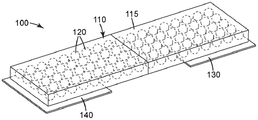
Fig. 1 is a block diagram illustrating an example system or apparatus including a waveguide with a high dielectric resonator in accordance with one or more techniques of this disclosure. In the system 100, a waveguide 110 is electromagnetically coupled to a transceiver (130, 140). The waveguide includes a substrate 115 and a plurality of HDR's 120 distributed in a pattern throughout the waveguide 110. Waveguide 110 receives a signal from one of the two transceivers that propagates through HDR 120 and into the opposite end of waveguide 110. The signal may be, for example, an electromagnetic wave, a sound wave, or the like. In some examples, the signal is a 60GHz millimeter wave signal. The signal exits the waveguide 110 through one of the two transceivers. In the example shown, the waveguide is coupled with two transceivers; however, the waveguide may be coupled with three or more transceivers. In some cases, one or more of the transceivers are only transmitters. In some cases, one or more of the transceivers are only receivers.
In some embodiments, the substrate 115 can include a material, such as, for example Quartz glass, cordierite, borosilicate glass, perfluoroalkoxy, polyurethane, polyethylene, fluorinated ethylene propylene, and the like. In some cases, the substrate may include, for example, copper, brass, silver, aluminum, or other metals having low bulk resistivity. In one example,
 waveguide 110 has dimensions of 2.5mm by 1.25mm, and is made of a material having an εrA relative dielectric constant of 2.1 and a loss tangent of 0.0002 Is made with a 1mm thick aluminum plating on the inner wall of the
 waveguide 110.
The waveguide 110 is made of a low relative permittivity material (such as, for example ) And (4) forming a structure. In other examples, the substrate portion of the
 waveguide 110 may be made of materials such as: quartz glass, cordierite, borosilicate glass, perfluoroalkoxy, polyethylene, or fluorinated ethylene propylene. In some examples, the waveguide 110 has a trapezoidal shape with a tapered end positioned adjacent to one end of the waveguide 110. In one example, waveguide 110 is formed from a length of 46cm and a thickness of 25.5mm The substrate is formed with HDR spheres having a relative dielectric constant of 40, a radius of 8.5mm, a lattice constant of 25.5mm, with a spacing of 5mm between the
 transceiver 130 and the waveguide 110.
In some embodiments, the waveguide 110 comprises a plurality of HDR 120 arranged within a substrate 115 such that the lattice distance between adjacent HDR is less than the wavelength of the electromagnetic wave designed to propagate. In some embodiments, the waveguide 110 comprises a plurality of HDR 120 arranged in an array within a substrate 115. In some examples, the array is a two-dimensional grid array. In some cases, the array is a regular array. The regular array may be, for example, a periodic array such that adjacent HDR's have approximately the same distance along a dimension.
In some examples, the resonant frequency of the HDR is selected to match the frequency of the electromagnetic wave. In some examples, the resonant frequency of the plurality of resonators is within a millimeter wave band. In one example, the resonant frequency of the plurality of resonators is 60 GHz. Each of these HDR's can then refract the wave towards the respective HDR with the same vertical arrangement in a single vertical line of three equally spaced HDR's. A standing wave oscillating with a large amplitude is formed in the waveguide 110.
The HDR 120 may also be arranged in other arrays at a particular pitch. For example, the HDRs 120 are arranged in rows at predetermined intervals. In some cases, HDR can be arranged in a three-dimensional array. For example, HDR can be arranged in a cylinder, stacked matrix, tube, etc. HDR 120 may be spaced in such a way that the resonance of one HDR transfers energy to any surrounding HDR. This spacing is related to the Mie resonance of HDR 120 and system efficiency. The spacing may be selected to improve system efficiency by taking into account the wavelength of any electromagnetic waves in the system. Each HDR 120 has a diameter and a lattice constant. In some examples, the lattice constant and the resonant frequency are selected based at least in part on the relative dielectric constants of the waveguide and the HDR. The lattice constant is the distance from the center of one HDR to the center of the neighboring HDR. In some examples, the HDR 120 may have a lattice constant of 1 mm. In some examples, the lattice constant is less than a wavelength of the electromagnetic wave.
The ratio of the diameter of the HDR to the lattice constant of the HDR (diameter D/lattice constant a) can be used to characterize the geometric arrangement of the HDR 120 in the waveguide 110. This ratio can vary with the relative dielectric constant contrast of the substrate and HDR. In some examples, the ratio of the diameter to the lattice constant of the resonator is less than one. In one example, D may be 0.7mm and a may be 1mm, with a ratio of 0.7. The higher the ratio, the lower the coupling efficiency of the waveguide becomes. In one example, the maximum limit of the lattice constant of the geometric arrangement of the HDR 120 shown in fig. 1 will be the wavelength of the emitted wave. The lattice constant should be less than the wavelength, but for strong efficiency, the lattice constant should be much smaller than the wavelength. Of these parametersThe relative dimensions may vary with the relative dielectric constant contrast of the substrate and HDR. The lattice constant may be selected to achieve a desired performance within the wavelength of the emitted wave. In one example, the lattice constant may be 1mm and the wavelength may be 5mm, i.e. the lattice constant is one fifth of the wavelength. Generally, the wavelength (λ) is the wavelength in an air medium. If another dielectric material is used for the medium, the wavelength of this formula should be λeffAlternatively, the formula is:

wherein epsilonrIs the relative dielectric constant of the dielectric material.
The high relative permittivity contrast between the HDR 120 and the substrate 115 of the waveguide 110 causes excitation in well-defined resonant modes of the HDR 120. In other words, the material forming the HDR 120 has a high relative permittivity compared to the relative permittivity of the substrate of the waveguide 110. Higher contrast will provide higher performance and therefore the relative permittivity of the HDR 120 is an important parameter in determining the resonance characteristics of the HDR 120. The low contrast can result in weak resonance of the HDR 120 as energy will leak into the substrate of the waveguide 110. The high contrast provides an approximation to perfect boundary conditions, which means that little energy leaks into the substrate of the waveguide 110. This approximation may be assumed for the following example: wherein the material forming the HDR 120 has a relative permittivity that is more than 5-10 times the relative permittivity of the substrate 115 of the waveguide 110. In some cases, the relative dielectric constant of each of the HDR's 120 is at least five times the relative dielectric constant of the substrate 115. In some examples, the relative permittivity of each resonator of the plurality of resonators is at least two times greater than the relative permittivity of the substrate 115. In other examples, each resonator of the plurality of resonators has a relative permittivity that is at least ten times greater than the relative permittivity of the substrate 115. For a given resonant frequency, the higher the relative permittivity, the smaller the dielectric resonator and the more concentrated the energy within the dielectric resonator. In some embodiments, each of the plurality of resonators has a relative permittivity greater than 20. In some cases, each of the plurality of resonators has a relative permittivity greater than 50. In some cases, each of the plurality of resonators has a relative permittivity greater than 100. In some cases, each of the plurality of resonators has a relative permittivity within a range of 200 to 20,000.
In some embodiments, HDR can be treated to increase relative dielectric constant. For example, at least one of the HDRs is heat treated. As another example, at least one of the HDR is sintered. In such examples, at least one of the HDR may be sintered at a temperature above 600 ℃ for a period of two to four hours. In other cases, at least one of the HDR may be sintered at a temperature above 900 ℃ for a period of two to four hours. In some embodiments, the substrate comprises Quartz glass, cordierite, borosilicate glass, perfluoroalkoxy, polyurethane, polyethylene, fluorinated ethylene propylene, combinations thereof, and the like. In some cases, the substrate has a relative dielectric constant in the range of 1 to 20. In some cases, the substrate has a relative dielectric constant in the range of 1 to 10. In some cases, the substrate has a relative dielectric constant in the range of 1 to 7. In some cases, the substrate has a relative dielectric constant in the range of 1 to 5.
In some examples, the plurality of resonators are made of a ceramic material. HDR 120 can be made from any of a variety of ceramic materials, including, for example, BaZnTa oxide, bazncobb oxide, zirconium-based ceramic, titanium-based ceramic, barium titanate-based material, titanium oxide-based material, Y5V compositions, and X7R compositions, among others. The HDR 120 may be made of at least one of: doped or undoped barium titanate (BaTiO)3) Barium strontium titanate (BaSrTiO)3) Y5V composition, X7R composition, TiO2(titanium dioxide), calcium copper titanate (CaCu)3Ti4O12) Lead zirconate titanate (PbZr)xTi1-xO3) Lead titanate (PbTiO)3) Lead magnesium titanate (PbMgTiO)3) Lead magnesium niobate-lead titanate (Pb (Mg)1/3Nb2/3)O3.-PbTiO3) Titanium iron tantalate (FeTiTaO)6) NiO (La) co-doped with Li and Ti1.5Sr0.5NiO4、Nd1.5Sr0.5NiO4) And combinations thereof. In one example, the HDR 120 may have a relative dielectric constant of 40. In some embodiments, the waveguide is flexible. For example, the waveguide has a substrate of a siloxane composite and a waveguide made of BaTiO3The HDR is made.
Although illustrated as a sphere in fig. 1 for purposes of example, in other examples, the HDR 120 may be formed in a variety of different shapes. In other examples, each of the HDRs 120 may have a cylindrical shape. In still other examples, each of the HDR 120 may have a cube or other parallelepiped shape. In some examples, each of the HDR may have a rectangular shape or an elliptical shape. The HDR 120 may take on other geometries. The function of the HDR 120 may vary depending on the shape, as described in further detail below with reference to fig. 4A-4C.
The waveguide 110 with HDR 120 can be used in a variety of systems including, for example, body area networks, body sensor networks, 60GHz communications, underground communications, and the like. In some examples, a waveguide, such as waveguide 110 of fig. 1, may be formed to include a substrate and a plurality of high dielectric resonators, wherein the arrangement of HDR within the substrate is controlled during formation such that HDR are spaced apart from each other by a selected distance. The distance between HDR, i.e. the lattice constant, may be selected based on the wavelength of the electromagnetic wave signal to be used with the waveguide. For example, the lattice constant may be much smaller than the wavelength. In some examples, the substrate material of the waveguide 110 may be divided into multiple portions during formation of the waveguide 110. Where there is a determination of the location of the HDR plane, the substrate material may be segmented. Hemispherical grooves may be included in portions of the substrate material at the location of each HDR. In other examples with HDR of different shapes, semi-cylindrical or semi-rectangular trenches may be included in the substrate material. The HDR may then be placed in a trench of substrate material. Portions of the substrate material may then be combined to form a single waveguide structure in which the HDR is embedded. Although fig. 1 shows a communication device/system with two transceivers coupled to a waveguide, one of ordinary skill can readily design a communication device/system with multiple transceivers coupled to one or more waveguides.
Fig. 2A illustrates a conceptual diagram of one example of a communication system 200A using a waveguide with HDR; FIG. 2B is an EM amplitude plot for communication system 200A; fig. 2C shows a comparison graph of communication system 200A with and without HDR. The communication system 200A includes a closed loop waveguide 210A coupled to two transceivers 230A and 240A, where the transceiver 230A can be better seen in fig. 2B. Waveguide 210A includes a substrate 215A and a plurality of HDR 220A. Transceiver 230A receives the 2.4GHz EM wave signal and propagates the signal via waveguide 210A. As shown in the graph in fig. 2B, the EM field strength is stronger at transceiver 230A and remains greater than 5.11V/m along HDR 220A. As shown in fig. 2C, at 2.4GHz, the S-parameter is-38.16 dB for the waveguide with HDR as shown in fig. 2A, and-80.85 dB for the waveguide without HDR, where the S-parameter describes the signal relationship between the two transceivers.
Fig. 2D illustrates a conceptual diagram of one example of a communication system 200D using a waveguide with HDR; FIG. 2E is an EM amplitude plot of communication system 200D; fig. 2F shows a comparison graph of communication system 200D with and without HDR. The communication system 200D includes an "L" shaped waveguide 210D coupled to two transceivers 230D and 240D. Waveguide 210D includes a substrate 215D and a plurality of HDR 220D. Transceiver 240D receives the 2.4GHz EM wave signal and propagates the signal through waveguide 210D. As shown in the graph in fig. 2D, the EM field strength is stronger at transceiver 240D and remains greater than 5.11V/m along HDR 220A. As shown in FIG. 2F, at 2.4GHz, the S-parameter is-29.68 dB for the waveguide with HDR shown in FIG. 2C and-45.38 dB for the waveguide without HDR.
Fig. 3A-3G illustrate some exemplary arrangements of HDR. These figures use circles to represent HDR; however, each HDR may use any configuration of HDR described herein. Fig. 3A shows one example of a waveguide 300A having multiple HDR 310A arranged in an array with approximately the same arrangement between each row. In some cases, four adjacent HDR s in two adjacent rows form a rectangular shape 315A. In some cases, 315A is generally square, i.e., the distance between two adjacent rows is the same distance as the distance between two adjacent HDR in a row. In some implementations, adjacent HDR in a row have approximately the same spacing. In some embodiments, for a row with a desired spacing between adjacent HDR S, the distance between any two adjacent HDR S in the row is in the range of S (1 ± 40%). Fig. 3B shows another example of a waveguide 300B having multiple HDR 310B arranged in an array with a different arrangement between two adjacent rows. In some cases, four adjacent HDR in two adjacent rows form a parallelogram 315B. In some cases, four HDR in every two other rows form a rectangular shape 317B. In some cases, each two adjacent rows have approximately the same distance.
Fig. 3C shows one example of a waveguide 300C having multiple HDR 310C arranged in an array with a different arrangement between two adjacent rows. In some cases, four adjacent HDR s in three adjacent rows form a square 315C. In some other cases, the distance between two adjacent HDR s in a row is typically the same as the distance between two adjacent HDR s between two rows. In some cases, four HDR in every two other rows form a rectangular shape 317C. In some cases, rectangular shape 317C is a square.
Fig. 3D shows one example of a waveguide 300D having multiple HDR 310D arranged in a pattern, where the HDR are of various sizes and/or shapes. In some cases, at least two HDR are of different sizes and/or shapes from each other. In some cases, the first set of HDR has a different size and/or shape than the second set of HDR. In some cases, the first set of HDR is formed of a material having a first relative permittivity that is different from a second relative permittivity of a material used for the second set of HDR. The modes of a set of HDR of respective sizes, shapes and/or materials may use any of the modes described herein, such as the modes shown in fig. 3A-3C. In the example shown in fig. 3D, four adjacent HDR s in two adjacent rows form a rectangular shape 315D. Fig. 3E shows an example of a waveguide 300D with multiple HDR 310D arranged in a controlled manner, such that the distance of adjacent HDR is smaller than the wavelength of the EM wave to be propagated. In some cases, the HDR 310D is of substantially the same size, shape, and/or material. In some other cases, the HDR 310D may be of a different size, shape, and/or material. In such cases, the HDR is set in such a way that the distance of adjacent HDR within the same group is smaller than the wavelength of the EM wave to be propagated. In some cases, as shown in fig. 3D and 3E, HDR of different sizes and/or shapes may propagate EM waves in different wavelength ranges. For example, in the case of using a material having a relative dielectric constant of 40, a small HDR of 0.68mm in diameter propagates EM waves in the 60GHz range; medium HDR with a diameter of 7mm propagates EM waves in the 5.8GHz range; and a large HDR of 17mm diameter propagates EM waves in the 2.4GHz range.
In some embodiments, HDR in a waveguide may comprise different sets of HDR made of different dielectric materials, such that each set of HDR has a different relative dielectric constant and is capable of propagating EM waves of a particular wavelength range. In some cases, the waveguide includes a first set of HDR's having a first relative permittivity and a second set of HDR's having a second relative permittivity different from the first relative permittivity. In some configurations, a first set of HDR is set in a first mode and a second set of HDR is set in a second mode, where the second mode may be the same as or different from the first mode. In some configurations as shown in fig. 3D, each set of HDR is set in a regular pattern. In some configurations as shown in fig. 3E, each set of HDR is set in a controlled manner such that the distance of adjacent HDR is less than the wavelength of the EM wave to be propagated.
Fig. 3F shows an example of a waveguide 300F with one row of HDR 310F. As shown, adjacent HDR 310F may have approximately the same distance. In some other cases, the distance between adjacent HDR 310F is in the range of S (1 ± 40%), where S is the desired distance between adjacent HDR 310F. In some cases, the HDR 310F is set in a controlled manner such that the distance of adjacent HDR is less than the wavelength of the EM wave to be propagated. In some implementations, the waveguide 300F can include an attachment device, such as an adhesive tape, an adhesive segment, one or more hook or loop fasteners, or the like.
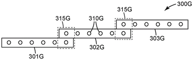
Fig. 3G shows an example of a waveguide 300G in a stack. Waveguide 300G has three sections 301G, 302G and 303G. Each segment (301G, 302G, or 303G) includes multiple HDR 310G. Each section (301G, 302G, or 303G) may have HDR 310G set in any of the modes shown in fig. 3A-3F. In the example shown, the HDRs 310G of each section are arranged in rows. Two adjacent sections have an overlapping section 315D, the overlapping section 315D comprising at least two HDR to allow EM wave propagation across the sections.
Fig. 4A-4C are block diagrams illustrating various shapes of structures that may be used for HDR according to one or more techniques of this disclosure. Fig. 4A illustrates an example of spherical HDR in accordance with one or more techniques of this disclosure. The spherical HDR 80 may be made from a variety of ceramic materials, including, for example, BaZnTa oxide, baznconib oxide, Zr-based ceramic, titanium-based ceramic, barium titanate-based material, titania-based material, Y5V composition, X7R composition, and the like. The HDR 82 and 84 of fig. 4B and 4C may be made of similar materials. The spherical HDR 80 is symmetric so the angle of incidence of the antenna and the emitted wave do not affect the system as a whole. The relative dielectric constant of the HDR sphere 80 is positively correlated with the resonant frequency. For example, at the same resonant frequency, the size of the HDR sphere 80 may be reduced by using a material with a higher relative dielectric constant. The TM resonance frequency of HDR sphere 80 can be calculated using the following equation for mode S and pole n:

the TE resonant frequency of the HDR sphere 80 can be calculated using the following equation for mode S and pole n:

where a is the radius of the cylindrical resonator.
Fig. 4B is a block diagram illustrating an example of cylindrical HDR in accordance with one or more techniques of the present disclosure. The cylindrical HDR 82 is not symmetric about all axes. Thus, as opposed to the symmetric spherical HDR 80 of fig. 4A, depending on the angle of incidence, the angle of incidence of the antenna and the emitted wave relative to the cylindrical HDR 82 can produce a polarizing effect on the wave as it passes through the cylindrical HDR 82. TE to isolate cylindrical HDR 8201nThe appropriate resonant frequency of a mode can be calculated using the following equation:

where a is the radius of the cylindrical resonator and L is its length. a and L are both in millimeters. Resonant frequency fGHzIn gigahertz. The formula is accurate to about 2% in the following range: 0.5<a/L<2 and 30<εr<50。
FIG. 4C is a block diagram illustrating an example of cube HDR in accordance with one or more techniques of this disclosure. The cube HDR 84 is not symmetric about all axes. Thus, as opposed to the symmetric spherical HDR 80 of fig. 4A, the angle of incidence of the antenna and the emitted wave relative to the cylindrical HDR 82 can produce a polarizing effect on the wave as it passes through the cube HDR 84. Approximately, the lowest resonant frequency of cube HDR 84 is:

where a is the cube side length and c is the speed of light in air.
Fig. 4D is a block diagram illustrating an example of a spherical HDR 88 coated with a substrate 90. This can be used to control the spacing between HDR. In some cases, this may be used during the manufacturing process to control the regular lattice constant of the HDR array. For example, the diameter of a spherical HDR 88 is 17mm, with a coating thickness of 4.25mm for the substrate 90.
Fig. 5A shows an example of a body area network ("BAN") 500A using a waveguide 510A with HDR. Waveguide 510A may be configured using any of the configurations described herein. As shown in the example, waveguide 510A is disposed on garment 520A or integrated with garment 520A. In some cases, waveguide 510A may be in the form of a strip attachable to garment 520A. In some other cases, waveguide 510A is an integral part of apparel 520A. In some cases, BAN 500A includes several miniaturized body sensor units ("BSUs") 530A. The BSU 530A may include, for example, a blood pressure sensor, an insulin pump sensor, an ECG sensor, an EMG sensor, a motion sensor, and the like. BSU 530A is electrically coupled to waveguide 510A. "electrically coupled" means electrically connected or wirelessly connected. In some cases, BAN 500A may be used with sensors (e.g., helmets, body armor, equipment in use, etc.) that are applied to a person's surroundings.
In some cases, one or more components of BSU 530A are integrated with a transceiver (not shown) that is electromagnetically coupled to waveguide 510A. In some cases, one or more components of BSU 530A are disposed on garment 520A. In some cases, one or more components of BSU 530A are disposed on the body and electromagnetically coupled to transceiver or waveguide 510A. BSU 530A may wirelessly communicate with control unit 540A via waveguide 510A. The control unit 540A may also communicate via a cellular network 550A or a wireless network 560A.
Fig. 5B illustrates an example of a waveguide 510B for use in the communication system 500B. Communication system 500B includes two communication components 520B and 530B that propagate EM waves. For example, component 520B and/or 530B includes a dielectric resonator. As another example, a dielectric resonator is disposed on a surface of component 520B and/or 530B. Communication system 500B also includes a waveguide 510B disposed between the two components 520B and 530B and capable of propagating EM waves from one component to the other. Waveguide 510B may be configured using any of the configurations described herein.
Fig. 5C shows an example of a communication system 500C to be used with an enclosure 540C (e.g., a vehicle). The communication system 500C includes a transceiver 520C located within an enclosure 540C, a transceiver 530C located outside the enclosure 540C or at a location that allows for airborne propagation of EM waves, and a waveguide 510C electromagnetically coupled to the transceivers 520C and 530C. In the example of an enclosure that interrupts EM wave propagation, the communication system 500C allows for bidirectional or unidirectional communication of signals carried in EM waves into and out of the enclosure. Waveguide 510C may be configured using any of the configurations described herein.
Fig. 6 is a block diagram illustrating one embodiment of a communication device 600 to be used with a barrier structure 650. A blocking structure is a structure that will cause significant loss or disruption of wireless signals within a particular wavelength. The blocking structure may cause reflection and refraction of the transmitted wireless signal and result in signal loss. For example, the barrier structure may be a concrete wall, for example, with metal, metalized glass, leaded glass, metal walls, and the like. In some cases, the communication device 600 is a passive device capable of capturing wireless signals on one end (e.g., the front of a wall), directing the signals in a predefined manner (e.g., around the wall), and re-transmitting the wireless signals on the other end (e.g., the back side of the wall). The communication device 600 includes a first passive coupling device 610, a second passive coupling device 620, and a waveguide 630. The waveguide 630 may use any of the waveguide configurations described herein.
The blocking structure 650 has a first side 651 and a second side 652. In some cases, first side 651 is adjacent to second side 652. In some cases, the first side 651 is opposite the second side 652. In some cases, the first coupling device is disposed adjacent to a first side of the blocking structure and is configured to capture incident electromagnetic waves 615 (otherwise referred to as wireless signals). The second coupling means 620 is arranged adjacent to the second side of the barrier structure. The waveguide 630 is electromagnetically coupled to the first and second coupling means (610,620) and is disposed around the barrier structure 650. In some cases, the waveguide 630 has a resonant frequency that matches the first and second coupling devices (610, 620). The waveguide 630 is configured to propagate the electromagnetic wave 615 captured by the first coupling device 610 towards the second coupling device. The second coupling device 620 is configured to emit an electromagnetic wave 625 corresponding to the incident electromagnetic wave 615. In some embodiments, the electromagnetic wave may propagate in the opposite direction such that the second coupling device 620 may capture the incident electromagnetic wave, couple the electromagnetic wave into the waveguide 630, the waveguide 630 propagates the electromagnetic wave towards the first coupling device 610, and the first coupling device 610 may emit the electromagnetic wave.
In some embodiments, at least one of the two coupling devices (610,620) is a passive EM collector designed to capture EM waves within a particular wavelength range. The coupling device may be, for example, a dielectric lens, a patch antenna, a yagi antenna, a metamaterial coupling element, or the like. In some cases, the coupling device has a gain of at least 1. In some cases, the coupling device has a gain in the range of 1.5 to 3. In some cases, the coupling device has a gain of at least 1. In some cases, if directionality is desired, such as coupling only energy from a particular source or blocking energy from other angles or sources (such as interference sources), the gain of the coupling device may be at least 10 to 30.
Fig. 7A-7D illustrate some examples of coupling devices. In fig. 7A, the coupling device 710A is a dielectric lens. The communication device 700A includes a coupling device 710A and a waveguide 730 electromagnetically coupled to the coupling device 710A. Coupling device 710A is disposed adjacent to one side of blocking structure 750. The dielectric lens 710A may collect electromagnetic waves from the surrounding environment and couple the electromagnetic waves to the waveguide 730. In fig. 7B, the coupling device 710B is a patch antenna. The communication device 700B includes a coupling device 710B and a waveguide 730 electromagnetically coupled to the coupling device 710B. Coupling means 710B is disposed adjacent to one side of barrier structure 750. In the example shown, the patch antenna 710B includes a patch antenna array 712B that can collect electromagnetic waves from the surrounding environment, a feed network 714B that transmits the electromagnetic waves, a secondary patch 716B that couples the electromagnetic waves to a waveguide 730, and a ground 718B.
In fig. 7C, the coupling device 710C is a yagi antenna. The communication device 700C includes a coupling device 710C and a waveguide 730 electromagnetically coupled to the coupling device 710C. The coupling device 710C is disposed adjacent to one side of the blocking structure 750. In the example shown, yagi antenna 710C includes a guide 712C that can collect electromagnetic waves from the surrounding environment, a ground plane/reflector 716C, a support 718C, and a patch 714C that couples the electromagnetic waves to a waveguide 730. The support 718C may be formed of an electrically non-conductive material.
Fig. 7D illustrates one example of a coupling device 710D. The coupling device 710D is a metamaterial coupling element including a top layer 712D and a ground element 720D. The top layer 712D is disposed on one side of the waveguide 730 and the ground element 720D is disposed on the opposite side of the waveguide 730. In some embodiments, the top layer 712D may be formed of a solid metal. The top layer 712D includes a plurality of ring-shaped elements 715D disposed thereon. In some embodiments, the ring element 715D may be disposed on any dielectric substrate, or directly on the surface of the waveguide 730. The ring element 715D may be made of a conductive material, such as copper, silver, gold, etc. In some cases, the loop element may be printed on the top layer 712D. In some cases, the grounding element 720D may be a sold metal ground plane. In some cases, the ground element 720D can have the same pattern of ring elements 715D as the top layer 712D (not shown). In some cases, the top layer 712D may include a conductive layer, wherein the conductive layer is etched at the ring element 715D.
Exemplary embodiments
Item a1. an apparatus, comprising:
two of the transceivers are used as a transceiver,
a waveguide for propagating electromagnetic waves and electromagnetically coupled to two transceivers, the waveguide comprising a substrate and a plurality of resonators arranged in a pattern, the plurality of resonators having a resonant frequency,
wherein each resonator of the plurality of resonators has a relative permittivity greater than a relative permittivity of the substrate,
wherein at least two of the plurality of resonators are spaced apart according to a lattice constant that defines a distance between a center of a first one of the resonators and a center of an adjacent second one of the resonators.
Item a2. the apparatus of item a1, further comprising:
a substrate, wherein the waveguide is disposed on or integrated with the substrate.
Item a3 the apparatus of item a2, wherein the two transceivers are disposed on the substrate.
The device of any one of items a1-A3, wherein the waveguide is flexible.
The device of any one of items a1-a4, wherein the plurality of resonators are disposed in or on the substrate.
The device of any of items a1-a5, wherein the substrate is coated on at least some of the plurality of resonators.
Item A7. the apparatus of any one of items A1-A6, wherein at least one of the two transceivers is a transmitter.
Item A8. is the apparatus of any one of items a1-a7, further comprising:
a first sensor electrically coupled to a first transceiver of the two transceivers and configured to generate a first sensing signal.
Item A9. the apparatus of item a8, wherein the first transceiver is configured to transmit the first sensing signal to the second transceiver via the waveguide.
Item a10. the apparatus of item A8, further comprising:
a second sensor electrically coupled to a second transceiver of the two transceivers.
The apparatus of any of items a1-a10, wherein the lattice constant is less than the wavelength of the electromagnetic wave.
The apparatus of any one of items a1-a11, wherein a resonant frequency of the plurality of resonators is selected based at least in part on a frequency of the electromagnetic wave.
The apparatus of any of items a1-a12, wherein a resonant frequency of the plurality of resonators is selected to match a frequency of the electromagnetic wave.
The apparatus of any of items a1-a13, wherein a ratio of a diameter to a lattice constant of the resonator is less than one.
The apparatus of any one of items a1-a14, wherein each resonator of the plurality of resonators has a relative permittivity that is at least five times the relative permittivity of the substrate.
The device of any one of items a1 to a15, wherein each resonator of the plurality of resonators has a relative permittivity that is at least ten times the relative permittivity of the substrate.
The apparatus of any of items a1-a16, wherein a resonant frequency of the plurality of resonators is in a millimeter wave range.
The apparatus of any of items a1-a17, wherein a resonant frequency of the plurality of resonators is approximately 60 GHz.
The apparatus of any one of items a1-a18, wherein a resonant frequency of the plurality of resonators is in an infrared frequency range.
The apparatus of any one of items a1-a19, wherein the plurality of resonators are made of a ceramic material.
The apparatus of any of items a1-a20, wherein each resonator of the plurality of resonators has a relative permittivity greater than 10.
The apparatus of any of items a1-a21, wherein each resonator of the plurality of resonators has a relative permittivity greater than 20.
The apparatus of any of items a1-a22, wherein each resonator of the plurality of resonators has a relative permittivity greater than 50.
The apparatus of any of items a1-a23, wherein each resonator of the plurality of resonators has a relative permittivity greater than 100.
The apparatus of any one of items a1-a24, wherein each resonator of the plurality of resonators has a relative dielectric constant in the range of 200 to 20,000.
The apparatus of any one of items a1-a25, wherein the plurality of resonators are made of: doped or undoped barium titanate (BaTiO)3) Barium strontium titanate (BaSrTiO)3) Y5V composition, X7R composition, TiO2(titanium dioxide), calcium copper titanate (CaCu)3Ti4O12) Lead zirconate titanate (PbZr)xTi1-xO3) Lead titanate (PbTiO)3) Lead magnesium titanate (PbMgTiO)3) Lead magnesium niobate-lead titanate (Pb (Mg)1/3Nb2/3)O3.-PbTiO3) Titanium iron tantalate (FeTiTaO)6) NiO (La) co-doped with Li and Ti1.5Sr0.5NiO4、Nd1.5Sr0.5NiO4) And combinations thereof.
The apparatus of any of items a1-a26, wherein at least one of the plurality of resonators is heat treated.
The apparatus of any of items a1-a27, wherein at least one of the plurality of resonators is sintered.
Item a29. the device of item a28, wherein at least one of the plurality of resonators is sintered at a temperature greater than 600 ℃ for a period of two to four hours.
Item a30 the device of item a28, wherein at least one of the plurality of resonators is sintered at a temperature greater than 900 ℃ for a period of two to four hours.
Item a31. the device of item a4, wherein the substrate comprises at least one of: quartz glass, cordierite, borosilicate glass, perfluoroalkoxy, polyurethane, polyethylene, and fluorinated ethylene propylene.
The device of any one of items a1-a31, wherein the substrate has a relative dielectric constant in the range of 1 to 20.
The device of any one of items a1-a32, wherein the substrate has a relative dielectric constant in the range of 1 to 10.
The device of any one of items a1-a33, wherein the substrate has a relative dielectric constant in the range of 1 to 7.
The device of any one of items a1-a34, wherein the substrate has a relative dielectric constant in the range of 1 to 5.
The apparatus of any of items a1-a35, wherein the plurality of resonators are formed to have one of a spherical, cylindrical, cubic, rectangular, or elliptical shape.
Item a37. a wearable device, comprising: the apparatus of clause a1.
Item a38. the wearable device of item a37, further comprising: one or more sensors, each sensor associated with a respective one of the two transceivers.
Item a39. the wearable device of item a38, wherein the transceiver is associated with two or more sensors.
Item a40. the wearable device of any of items a37-a39, wherein the wearable device is a garment.
Item a41. a wireless communication system, comprising:
a first transceiver and a second transceiver; and
a regular array of resonators forming a waveguide extending between and coupled to the first transceiver and the second transceiver.
Item a42. the wireless communication system of item a41, wherein the waveguide comprises a nonlinear section.
Item a43. a waveguide for propagating electromagnetic waves, comprising:
a plurality of resonators having a resonance frequency of,
wherein each resonator of the plurality of resonators is coated with a substrate,
wherein each resonator of the plurality of resonators has a relative permittivity greater than a relative permittivity of the substrate.
The waveguide of item a43, wherein each resonator of the plurality of resonators has a relative permittivity that is at least five times greater than a relative permittivity of the substrate.
The waveguide of item a43 or a44, wherein each resonator of the plurality of resonators has a relative permittivity that is at least ten times the relative permittivity of the substrate.
The waveguide of any of items a43-a45, wherein a resonant frequency of the plurality of resonators is selected to match a frequency of the electromagnetic wave.
The waveguide of any of items a43-a46, wherein the plurality of resonators are formed to have one of a spherical, cylindrical, cubic, rectangular, or elliptical shape.
Item a48. a waveguide for propagating electromagnetic waves, comprising:
a base material, a first metal layer and a second metal layer,
a first group of dielectric resonators, each dielectric resonator of the first group of dielectric resonators generally having a first size, an
A second set of dielectric resonators, each dielectric resonator of the second set of dielectric resonators generally having a second dimension greater than the first dimension,
wherein each of the first set of dielectric resonators and the second set of dielectric resonators has a relative permittivity greater than a relative permittivity of the substrate.
Item b1. a communication device for propagating electromagnetic waves around a barrier structure, comprising:
a passive coupling device disposed adjacent to the first side of the blocking structure and configured to capture electromagnetic waves,
an emitter disposed adjacent to the second side of the barrier structure,
a waveguide electromagnetically coupled to the coupling device and the transmitter and disposed around the blocking structure, the waveguide having a resonant frequency matched to the coupling device, the waveguide configured to propagate the electromagnetic waves captured by the coupling device,
wherein the transmitter is configured to re-radiate the electromagnetic wave.
Item B2. the apparatus of item B1, wherein the coupling device comprises a dielectric lens.
The apparatus of item B3. the apparatus of item B1 or B2, wherein the coupling apparatus comprises a patch antenna.
The apparatus of any of items B4. to B1-B3, wherein the coupling apparatus comprises a metamaterial coupling element.
Item B5. is the apparatus of any one of items B1-B4, wherein the waveguide comprises a substrate and a plurality of resonators.
Item B6. the apparatus of item B5, wherein the plurality of resonators are arranged in a pattern.
Item B7. the apparatus of item B5, wherein the plurality of resonators are arranged in an array.
Item B8. the apparatus of item B5, wherein at least two of the plurality of resonators are spaced according to a lattice constant that defines a distance between a center of a first one of the resonators and a center of an adjacent second one of the resonators.
Item B9. the device of item B7, wherein the lattice constant is less than the wavelength of the electromagnetic wave.
The device of any of items B1-B9, wherein a resonant frequency of the coupling device is selected to match a frequency of the electromagnetic wave.
The device of item B11. the device of item B7, wherein a ratio of the diameter of the resonator to the lattice constant is less than one.
The device of item B12. the device of item B5, wherein the plurality of resonators are disposed in or on the substrate.
The device of item B13. the device of item B5, wherein the substrate is coated on at least some of the plurality of resonators.
The apparatus of clause B14. the apparatus of clause B5, wherein the resonant frequency of the plurality of resonators is selected based at least in part on a frequency of the electromagnetic wave.
The apparatus of item B15. the apparatus of item B5, wherein the resonant frequency of the plurality of resonators is selected to match the frequency of the electromagnetic wave.
The apparatus of item B16. the apparatus of item B5, wherein a ratio of the diameter of the resonator to the lattice constant is less than one.
The apparatus of item B17. the apparatus of item B5, wherein each resonator of the plurality of resonators has a relative permittivity that is at least five times the relative permittivity of the substrate.
The apparatus of item B18. the apparatus of item B5, wherein each resonator of the plurality of resonators has a relative permittivity that is at least ten times the relative permittivity of the substrate.
The apparatus of any one of items B1-B18, wherein a resonant frequency of the waveguide is within a millimeter wave band.
The apparatus of any one of items B1-B19, wherein the resonant frequency of the waveguide is approximately 4.8 GHz.
The apparatus of any one of items B1-B20, wherein the resonant frequency of the waveguide is in the infrared frequency range.
The apparatus of item B22. the apparatus of item B5, wherein the plurality of resonators are made of a ceramic material.
The apparatus of item B23. the apparatus of item B5, wherein each of the plurality of resonators has a relative permittivity greater than 20.
The apparatus of item B24. the apparatus of item B5, wherein each of the plurality of resonators has a relative permittivity greater than 100.
The apparatus of item B25. the apparatus of item B5, wherein each of the plurality of resonators has a relative dielectric constant in the range of 200 to 20,000.
The apparatus of item B26. the apparatus of item B5, wherein the plurality of resonators are made of: doped or undoped barium titanate (BaTiO)3) Barium strontium titanate (BaSrTiO)3) Y5V composition, X7R composition, TiO2(titanium dioxide), calcium copper titanate (CaCu)3Ti4O12) Lead zirconate titanate (PbZr)xTi1-xO3) Lead titanate (PbTiO)3) Lead magnesium titanate (PbMgTiO)3) Lead magnesium niobate-lead titanate (Pb (Mg)1/3Nb2/3)O3.-PbTiO3) Titanium iron tantalate (FeTiTaO)6) NiO (La) co-doped with Li and Ti1.5Sr0.5NiO4、Nd1.5Sr0.5NiO4) And combinations thereof.
The apparatus of item B27. the apparatus of item B5, wherein at least one of the plurality of resonators is thermally treated.
The apparatus of item B28. the apparatus of item B5, wherein at least one of the plurality of resonators is sintered.
The apparatus of item B29. the apparatus of item B28, wherein at least one of the plurality of resonators is sintered at a temperature greater than 600 ℃ for a period of two to four hours.
The apparatus of item B30. the apparatus of item B28, wherein at least one of the plurality of resonators is sintered at a temperature greater than 900 ℃ for a period of two to four hours.
The device of item B31. according to item B5, wherein the substrate comprises at least one of: quartz glass, cordierite, borosilicate glass, perfluoroalkoxy, polyurethane, polyethylene, and fluorinated ethylene propylene.
The apparatus of any one of items B1-B31, wherein the second side is opposite the first side of the blocking structure.
The present invention should not be considered limited to the particular examples and embodiments described above, as such embodiments are described in detail to facilitate explanation of various aspects of the invention. On the contrary, the invention is to be construed as covering all aspects of the invention, including various modifications, equivalent processes and alternative arrangements falling within the spirit and scope of the invention as defined by the appended claims and their equivalents.
Claims (13)
1. An apparatus, comprising:
two transceivers; and
a dielectric waveguide for propagating electromagnetic waves and electromagnetically coupled to the two transceivers, the dielectric waveguide comprising a substrate and a plurality of resonators arranged in a pattern, the plurality of resonators having a resonant frequency,
wherein each resonator of the plurality of resonators has a relative permittivity greater than a relative permittivity of the substrate, and the plurality of resonators are spaced apart by a non-zero distance,
wherein at least two of the plurality of resonators are spaced according to a lattice constant that defines a distance between a center of a first one of the resonators and a center of an adjacent second one of the resonators,
wherein the plurality of resonators are a plurality of spaced apart ceramics having a non-linear resonant characteristic with a frequency in the range of 10GHz to 300GHz, and the dielectric waveguide is flexible.
2. The apparatus of claim 1, further comprising:
a substrate, wherein the dielectric waveguide is disposed on or integral with the substrate.
3. The device of claim 1, wherein the plurality of resonators are disposed in or on the substrate.
4. The device of claim 1, wherein the substrate is coated on at least some of the plurality of resonators.
5. The apparatus of claim 1, further comprising:
a first sensor electrically coupled to a first transceiver of the two transceivers and configured to generate a first sense signal.
6. The apparatus of claim 1, wherein the lattice constant is less than a wavelength of the electromagnetic wave.
7. The apparatus of claim 1, wherein the resonant frequencies of the plurality of resonators are selected based at least in part on a frequency of the electromagnetic wave.
8. The apparatus of claim 1, wherein each resonator of the plurality of resonators has a relative permittivity that is at least five times greater than a relative permittivity of the substrate.
9. A wearable device, comprising:
the apparatus of claim 1.
10. A wireless communication system, comprising:
a first transceiver and a second transceiver; and
a regular array of resonators disposed in a substrate, the regular array of resonators forming a dielectric waveguide extending between and coupled to the first transceiver and the second transceiver, and the plurality of resonators being spaced apart by a non-zero distance,
wherein the plurality of resonators are a plurality of spaced apart ceramics having a non-linear resonant characteristic with a frequency in the range of 10GHz to 300GHz, and the dielectric waveguide is flexible.
11. A dielectric waveguide for propagating an electromagnetic wave, comprising:
a plurality of resonators having a resonance frequency, and,
wherein each resonator of the plurality of resonators is coated with a dielectric substrate,
wherein each resonator of the plurality of resonators has a relative permittivity greater than a relative permittivity of the dielectric substrate, and the plurality of resonators are spaced apart by a non-zero distance,
wherein the plurality of resonators are a plurality of spaced apart ceramics having a non-linear resonant characteristic with a frequency in the range of 10GHz to 300GHz, and the dielectric waveguide is flexible.
12. The dielectric waveguide of claim 11, wherein each of the plurality of resonators has a relative permittivity that is at least five times greater than a relative permittivity of the dielectric substrate.
13. A waveguide for propagating an electromagnetic wave, comprising:
a dielectric substrate having a first surface and a second surface,
a first group of dielectric resonators, each dielectric resonator of the first group of dielectric resonators generally having a first size, an
A second set of dielectric resonators, each dielectric resonator of the second set of dielectric resonators generally having a second dimension greater than the first dimension,
wherein each of the first set of dielectric resonators and the second set of dielectric resonators has a relative permittivity greater than a relative permittivity of the dielectric substrate, and the plurality of resonators are spaced apart by a non-zero distance,
wherein the plurality of resonators are a plurality of spaced apart ceramics having a non-linear resonant characteristic with a frequency in the range of 10GHz to 300GHz, and the waveguide is flexible.
Applications Claiming Priority (3)
| Application Number | Priority Date | Filing Date | Title |
|---|---|---|---|
| US201562150379P | 2015-04-21 | 2015-04-21 | |
| US62/150,379 | 2015-04-21 | ||
| PCT/US2016/028038 WO2016172020A1 (en) | 2015-04-21 | 2016-04-18 | Waveguide with high dielectric resonators |
Publications (2)
| Publication Number | Publication Date |
|---|---|
| CN107534199A CN107534199A (en) | 2018-01-02 |
| CN107534199B true CN107534199B (en) | 2022-06-17 |
Family
ID=55858900
Family Applications (1)
| Application Number | Title | Priority Date | Filing Date |
|---|---|---|---|
| CN201680022375.5A Active CN107534199B (en) | 2015-04-21 | 2016-04-18 | Waveguide with high dielectric resonator |
Country Status (7)
| Country | Link |
|---|---|
| US (1) | US10658724B2 (en) |
| EP (1) | EP3286799B1 (en) |
| JP (1) | JP6869189B2 (en) |
| KR (1) | KR102597123B1 (en) |
| CN (1) | CN107534199B (en) |
| TW (1) | TWI711213B (en) |
| WO (1) | WO2016172020A1 (en) |
Families Citing this family (4)
| Publication number | Priority date | Publication date | Assignee | Title |
|---|---|---|---|---|
| US10411320B2 (en) | 2015-04-21 | 2019-09-10 | 3M Innovative Properties Company | Communication devices and systems with coupling device and waveguide |
| US10090589B2 (en) * | 2015-10-27 | 2018-10-02 | Microsoft Technology Licensing, Llc | Batteries as antenna for device |
| WO2018226657A1 (en) * | 2017-06-07 | 2018-12-13 | Rogers Corporation | Dielectric resonator antenna system |
| CN111164826B (en) | 2017-10-26 | 2023-07-21 | 3M创新有限公司 | Waveguide and communication system |
Family Cites Families (25)
| Publication number | Priority date | Publication date | Assignee | Title |
|---|---|---|---|---|
| CA1221750A (en) * | 1983-11-21 | 1987-05-12 | Richard D. Carver | Mounting dielectric resonators |
| US5889449A (en) * | 1995-12-07 | 1999-03-30 | Space Systems/Loral, Inc. | Electromagnetic transmission line elements having a boundary between materials of high and low dielectric constants |
| JP3134781B2 (en) | 1996-07-19 | 2001-02-13 | 株式会社村田製作所 | Multilayer dielectric line circuit |
| US5999308A (en) | 1998-04-01 | 1999-12-07 | Massachusetts Institute Of Technology | Methods and systems for introducing electromagnetic radiation into photonic crystals |
| US6297715B1 (en) | 1999-03-27 | 2001-10-02 | Space Systems/Loral, Inc. | General response dual-mode, dielectric resonator loaded cavity filter |
| US6590477B1 (en) * | 1999-10-29 | 2003-07-08 | Fci Americas Technology, Inc. | Waveguides and backplane systems with at least one mode suppression gap |
| EP1363351B1 (en) * | 2001-01-19 | 2008-08-06 | Matsushita Electric Industrial Co., Ltd. | High frequency circuit element and high frequency circuit module |
| AU2003230894A1 (en) | 2002-04-12 | 2003-10-27 | Massachusetts Institute Of Technology | Metamaterials employing photonic crystals |
| US7218190B2 (en) | 2003-06-02 | 2007-05-15 | The Trustees Of The University Of Pennsylvania | Waveguides and scattering devices incorporating epsilon-negative and/or mu-negative slabs |
| JP2005073168A (en) | 2003-08-27 | 2005-03-17 | Uniden Corp | Reradiation antenna system |
| US7470581B2 (en) | 2006-07-27 | 2008-12-30 | Hewlett-Packard Development Company, L.P. | Electromagnetic waveguide |
| KR20100051883A (en) | 2006-08-25 | 2010-05-18 | 레이스팬 코포레이션 | Antennas based on metamaterial structures |
| US7557758B2 (en) * | 2007-03-26 | 2009-07-07 | Broadcom Corporation | Very high frequency dielectric substrate wave guide |
| US7750869B2 (en) | 2007-07-24 | 2010-07-06 | Northeastern University | Dielectric and magnetic particles based metamaterials |
| US8723722B2 (en) | 2008-08-28 | 2014-05-13 | Alliant Techsystems Inc. | Composites for antennas and other applications |
| US8149181B2 (en) * | 2009-09-02 | 2012-04-03 | National Tsing Hua University | Dielectric resonator for negative refractivity medium |
| US8435427B2 (en) | 2010-08-26 | 2013-05-07 | 3M Innovative Properties Company | Compositions having non-linear current-voltage characteristics |
| JP5724439B2 (en) * | 2011-02-18 | 2015-05-27 | ソニー株式会社 | Electronic devices and modules mounted on electronic devices |
| EP2702697A1 (en) | 2011-04-28 | 2014-03-05 | Alliant Techsystems Inc. | Devices for wireless energy transmission using near -field energy |
| CN102480035A (en) | 2011-07-29 | 2012-05-30 | 深圳光启高等理工研究院 | Isotropous full-dielectric metamaterial and preparation method thereof |
| WO2013016928A1 (en) | 2011-07-29 | 2013-02-07 | 深圳光启高等理工研究院 | Isotropic all dielectric metamaterial and preparation method thereof, and composite material and preparation method |
| US9276645B2 (en) | 2012-03-29 | 2016-03-01 | GM Global Technology Operations LLC | Inductive charger for providing radio frequency (“RF”) signal to a portable electric device |
| ITTO20120477A1 (en) * | 2012-05-31 | 2013-12-01 | St Microelectronics Srl | NETWORK OF ELECTRONIC DEVICES FIXED TO A FLEXIBLE SUPPORT AND RELATIVE COMMUNICATION METHOD |
| US9564682B2 (en) | 2012-07-11 | 2017-02-07 | Digimarc Corporation | Body-worn phased-array antenna |
| KR102583381B1 (en) | 2015-04-21 | 2023-09-27 | 쓰리엠 이노베이티브 프로퍼티즈 컴파니 | Communication devices and systems with coupling devices and waveguides |
-
2016
- 2016-04-18 CN CN201680022375.5A patent/CN107534199B/en active Active
- 2016-04-18 JP JP2017555228A patent/JP6869189B2/en active Active
- 2016-04-18 EP EP16719176.6A patent/EP3286799B1/en active Active
- 2016-04-18 KR KR1020177033149A patent/KR102597123B1/en active IP Right Grant
- 2016-04-18 WO PCT/US2016/028038 patent/WO2016172020A1/en active Application Filing
- 2016-04-18 US US15/565,597 patent/US10658724B2/en active Active
- 2016-04-20 TW TW105112317A patent/TWI711213B/en active
Also Published As
| Publication number | Publication date |
|---|---|
| KR20170139076A (en) | 2017-12-18 |
| TW201705600A (en) | 2017-02-01 |
| US10658724B2 (en) | 2020-05-19 |
| KR102597123B1 (en) | 2023-11-03 |
| TWI711213B (en) | 2020-11-21 |
| EP3286799B1 (en) | 2022-06-01 |
| EP3286799A1 (en) | 2018-02-28 |
| CN107534199A (en) | 2018-01-02 |
| US20180115034A1 (en) | 2018-04-26 |
| JP6869189B2 (en) | 2021-05-12 |
| WO2016172020A1 (en) | 2016-10-27 |
| JP2018514164A (en) | 2018-05-31 |
Similar Documents
| Publication | Publication Date | Title |
|---|---|---|
| CN107534199B (en) | Waveguide with high dielectric resonator | |
| CN107534201B (en) | Communication device and system with coupling device and waveguide | |
| US10411320B2 (en) | Communication devices and systems with coupling device and waveguide | |
| US9601820B2 (en) | Dielectric waveguide comprised of a core surrounded by a cladding and forming integrated periodical structures | |
| US8432330B2 (en) | Electromagnetic screen | |
| US10170945B2 (en) | Yagi antenna shaped wireless power transmission apparatus | |
| CN107946775B (en) | Honeycomb-type-distribution adjustable plasma metamaterial narrow-band wave absorber | |
| US11677130B2 (en) | Waveguide and communication system | |
| KR102187041B1 (en) | System for transmitting and receiving wireless energy using metamaterial | |
| Tenuti et al. | Design of mantle cloaks through a System-by-Design approach | |
| Eggermont et al. | Investigation of metamaterial leaky wave antenna based on complementary split ring resonators | |
| Shirvani et al. | Gain Enhancement of Microstrip Patch Antenna and Array Antenna Using Different Metamaterial Structures for Telemedicine Applications | |
| Chanadee et al. | Efficiency Improvement in Wireless Power Transfer System at 2.45 GHz by Using Metamaterials | |
| Nespor et al. | Using metamaterials as electromagnetic lens for MR tomograph | |
| Rajinikanth | Certain Investigation of Multi Band Flexible Patch Antenna for Bio-Medical Applications | |
| KR20150017872A (en) | Matamaterial antenna using tunable capacitance | |
| Johnston et al. | Antennas for RF mote communications | |
| Lee et al. | On the Design of Millimetre Wave EBG Resonator Antenna Based on Woodpile Structure | |
| CN102809683A (en) | Electromagnetic wave sensor based on planar optical waveguide and metamaterial |
Legal Events
| Date | Code | Title | Description |
|---|---|---|---|
| PB01 | Publication | ||
| PB01 | Publication | ||
| SE01 | Entry into force of request for substantive examination | ||
| SE01 | Entry into force of request for substantive examination | ||
| GR01 | Patent grant | ||
| GR01 | Patent grant |