WO2024053564A1 - Photosensitive resin composition, resin film, and electronic device - Google Patents
Photosensitive resin composition, resin film, and electronic device Download PDFInfo
- Publication number
- WO2024053564A1 WO2024053564A1 PCT/JP2023/031925 JP2023031925W WO2024053564A1 WO 2024053564 A1 WO2024053564 A1 WO 2024053564A1 JP 2023031925 W JP2023031925 W JP 2023031925W WO 2024053564 A1 WO2024053564 A1 WO 2024053564A1
- Authority
- WO
- WIPO (PCT)
- Prior art keywords
- photosensitive resin
- resin composition
- mass
- polyimide
- film
- Prior art date
Links
- 239000011342 resin composition Substances 0.000 title claims abstract description 207
- 229920005989 resin Polymers 0.000 title claims description 129
- 239000011347 resin Substances 0.000 title claims description 129
- 229920001721 polyimide Polymers 0.000 claims abstract description 110
- 239000004642 Polyimide Substances 0.000 claims abstract description 87
- 238000000034 method Methods 0.000 claims abstract description 73
- XLYOFNOQVPJJNP-UHFFFAOYSA-N water Substances O XLYOFNOQVPJJNP-UHFFFAOYSA-N 0.000 claims abstract description 64
- 239000003504 photosensitizing agent Substances 0.000 claims abstract description 18
- 125000005462 imide group Chemical group 0.000 claims abstract 4
- 239000000758 substrate Substances 0.000 claims description 65
- 238000010438 heat treatment Methods 0.000 claims description 49
- 239000006087 Silane Coupling Agent Substances 0.000 claims description 41
- 150000001875 compounds Chemical class 0.000 claims description 36
- RYGMFSIKBFXOCR-UHFFFAOYSA-N Copper Chemical compound [Cu] RYGMFSIKBFXOCR-UHFFFAOYSA-N 0.000 claims description 31
- 229910052802 copper Inorganic materials 0.000 claims description 31
- 239000010949 copper Substances 0.000 claims description 31
- 239000002966 varnish Substances 0.000 claims description 31
- 150000003949 imides Chemical class 0.000 claims description 30
- 239000004593 Epoxy Substances 0.000 claims description 28
- 238000004519 manufacturing process Methods 0.000 claims description 28
- 239000003960 organic solvent Substances 0.000 claims description 22
- 239000007787 solid Substances 0.000 claims description 22
- 239000002904 solvent Substances 0.000 claims description 22
- XUIMIQQOPSSXEZ-UHFFFAOYSA-N Silicon Chemical compound [Si] XUIMIQQOPSSXEZ-UHFFFAOYSA-N 0.000 claims description 17
- 238000005259 measurement Methods 0.000 claims description 17
- 229910052710 silicon Inorganic materials 0.000 claims description 17
- 239000010703 silicon Substances 0.000 claims description 17
- 125000004018 acid anhydride group Chemical group 0.000 claims description 14
- BGTOWKSIORTVQH-UHFFFAOYSA-N cyclopentanone Chemical compound O=C1CCCC1 BGTOWKSIORTVQH-UHFFFAOYSA-N 0.000 claims description 14
- 125000003647 acryloyl group Chemical group O=C([*])C([H])=C([H])[H] 0.000 claims description 13
- 239000007864 aqueous solution Substances 0.000 claims description 13
- KRHYYFGTRYWZRS-UHFFFAOYSA-N Fluorane Chemical compound F KRHYYFGTRYWZRS-UHFFFAOYSA-N 0.000 claims description 10
- 238000011156 evaluation Methods 0.000 claims description 10
- 239000012299 nitrogen atmosphere Substances 0.000 claims description 10
- LLHKCFNBLRBOGN-UHFFFAOYSA-N propylene glycol methyl ether acetate Chemical compound COCC(C)OC(C)=O LLHKCFNBLRBOGN-UHFFFAOYSA-N 0.000 claims description 9
- 238000007363 ring formation reaction Methods 0.000 claims description 9
- 125000003368 amide group Chemical group 0.000 claims description 8
- 230000009477 glass transition Effects 0.000 claims description 8
- 238000001035 drying Methods 0.000 claims description 7
- 239000007921 spray Substances 0.000 claims description 7
- 238000004528 spin coating Methods 0.000 claims description 4
- 239000010410 layer Substances 0.000 description 173
- 239000004065 semiconductor Substances 0.000 description 59
- 239000003822 epoxy resin Substances 0.000 description 50
- 229920000647 polyepoxide Polymers 0.000 description 50
- -1 triazole compounds Chemical class 0.000 description 43
- YEJRWHAVMIAJKC-UHFFFAOYSA-N 4-Butyrolactone Chemical compound O=C1CCCO1 YEJRWHAVMIAJKC-UHFFFAOYSA-N 0.000 description 35
- 230000008569 process Effects 0.000 description 26
- 239000000243 solution Substances 0.000 description 26
- 238000006243 chemical reaction Methods 0.000 description 23
- 239000009719 polyimide resin Substances 0.000 description 23
- 238000003860 storage Methods 0.000 description 20
- 239000002253 acid Substances 0.000 description 17
- 230000015572 biosynthetic process Effects 0.000 description 17
- NIXOWILDQLNWCW-UHFFFAOYSA-M Acrylate Chemical compound [O-]C(=O)C=C NIXOWILDQLNWCW-UHFFFAOYSA-M 0.000 description 16
- 238000011161 development Methods 0.000 description 16
- 125000001153 fluoro group Chemical group F* 0.000 description 15
- 229910000679 solder Inorganic materials 0.000 description 14
- 238000003756 stirring Methods 0.000 description 13
- 238000003786 synthesis reaction Methods 0.000 description 13
- KFZMGEQAYNKOFK-UHFFFAOYSA-N Isopropanol Chemical compound CC(C)O KFZMGEQAYNKOFK-UHFFFAOYSA-N 0.000 description 12
- 238000005227 gel permeation chromatography Methods 0.000 description 12
- 125000000962 organic group Chemical group 0.000 description 12
- 239000000853 adhesive Substances 0.000 description 11
- KLSJWNVTNUYHDU-UHFFFAOYSA-N Amitrole Chemical group NC1=NC=NN1 KLSJWNVTNUYHDU-UHFFFAOYSA-N 0.000 description 10
- GTDPSWPPOUPBNX-UHFFFAOYSA-N ac1mqpva Chemical compound CC12C(=O)OC(=O)C1(C)C1(C)C2(C)C(=O)OC1=O GTDPSWPPOUPBNX-UHFFFAOYSA-N 0.000 description 10
- 230000001070 adhesive effect Effects 0.000 description 10
- 125000004432 carbon atom Chemical group C* 0.000 description 10
- 239000003054 catalyst Substances 0.000 description 10
- 150000004985 diamines Chemical class 0.000 description 10
- 125000000524 functional group Chemical group 0.000 description 10
- 239000000463 material Substances 0.000 description 10
- 239000000203 mixture Substances 0.000 description 10
- 239000000126 substance Substances 0.000 description 10
- 239000012298 atmosphere Substances 0.000 description 9
- 230000008859 change Effects 0.000 description 9
- 239000003999 initiator Substances 0.000 description 9
- 229910052751 metal Inorganic materials 0.000 description 9
- 238000006116 polymerization reaction Methods 0.000 description 9
- 239000000047 product Substances 0.000 description 9
- 238000012360 testing method Methods 0.000 description 9
- 125000002947 alkylene group Chemical group 0.000 description 8
- LZCLXQDLBQLTDK-UHFFFAOYSA-N ethyl 2-hydroxypropanoate Chemical compound CCOC(=O)C(C)O LZCLXQDLBQLTDK-UHFFFAOYSA-N 0.000 description 8
- 239000002184 metal Substances 0.000 description 8
- 150000003254 radicals Chemical class 0.000 description 8
- 239000002994 raw material Substances 0.000 description 8
- NVKGJHAQGWCWDI-UHFFFAOYSA-N 4-[4-amino-2-(trifluoromethyl)phenyl]-3-(trifluoromethyl)aniline Chemical group FC(F)(F)C1=CC(N)=CC=C1C1=CC=C(N)C=C1C(F)(F)F NVKGJHAQGWCWDI-UHFFFAOYSA-N 0.000 description 7
- 150000001252 acrylic acid derivatives Chemical class 0.000 description 7
- 125000003277 amino group Chemical group 0.000 description 7
- 230000000052 comparative effect Effects 0.000 description 7
- 238000010586 diagram Methods 0.000 description 7
- 238000000059 patterning Methods 0.000 description 7
- 230000000149 penetrating effect Effects 0.000 description 7
- 125000001997 phenyl group Chemical group [H]C1=C([H])C([H])=C(*)C([H])=C1[H] 0.000 description 7
- 238000012545 processing Methods 0.000 description 7
- 150000003852 triazoles Chemical group 0.000 description 7
- 229940042596 viscoat Drugs 0.000 description 7
- QQGYZOYWNCKGEK-UHFFFAOYSA-N 5-[(1,3-dioxo-2-benzofuran-5-yl)oxy]-2-benzofuran-1,3-dione Chemical compound C1=C2C(=O)OC(=O)C2=CC(OC=2C=C3C(=O)OC(C3=CC=2)=O)=C1 QQGYZOYWNCKGEK-UHFFFAOYSA-N 0.000 description 6
- OKKJLVBELUTLKV-UHFFFAOYSA-N Methanol Chemical compound OC OKKJLVBELUTLKV-UHFFFAOYSA-N 0.000 description 6
- WYURNTSHIVDZCO-UHFFFAOYSA-N Tetrahydrofuran Chemical compound C1CCOC1 WYURNTSHIVDZCO-UHFFFAOYSA-N 0.000 description 6
- IISBACLAFKSPIT-UHFFFAOYSA-N bisphenol A Chemical class C=1C=C(O)C=CC=1C(C)(C)C1=CC=C(O)C=C1 IISBACLAFKSPIT-UHFFFAOYSA-N 0.000 description 6
- 238000000576 coating method Methods 0.000 description 6
- 229910052731 fluorine Inorganic materials 0.000 description 6
- 125000004435 hydrogen atom Chemical group [H]* 0.000 description 6
- 238000007789 sealing Methods 0.000 description 6
- 238000005160 1H NMR spectroscopy Methods 0.000 description 5
- UFWIBTONFRDIAS-UHFFFAOYSA-N Naphthalene Chemical compound C1=CC=CC2=CC=CC=C21 UFWIBTONFRDIAS-UHFFFAOYSA-N 0.000 description 5
- 239000004793 Polystyrene Substances 0.000 description 5
- 239000011248 coating agent Substances 0.000 description 5
- 230000000694 effects Effects 0.000 description 5
- 239000003921 oil Substances 0.000 description 5
- 229920001187 thermosetting polymer Polymers 0.000 description 5
- TXBCBTDQIULDIA-UHFFFAOYSA-N 2-[[3-hydroxy-2,2-bis(hydroxymethyl)propoxy]methyl]-2-(hydroxymethyl)propane-1,3-diol Chemical compound OCC(CO)(CO)COCC(CO)(CO)CO TXBCBTDQIULDIA-UHFFFAOYSA-N 0.000 description 4
- NCAVPEPBIJTYSO-UHFFFAOYSA-N 4-hydroxybutyl prop-2-enoate;2-(oxiran-2-ylmethoxymethyl)oxirane Chemical compound C1OC1COCC1CO1.OCCCCOC(=O)C=C NCAVPEPBIJTYSO-UHFFFAOYSA-N 0.000 description 4
- PXHVJJICTQNCMI-UHFFFAOYSA-N Nickel Chemical compound [Ni] PXHVJJICTQNCMI-UHFFFAOYSA-N 0.000 description 4
- 125000000217 alkyl group Chemical group 0.000 description 4
- 125000006159 dianhydride group Chemical group 0.000 description 4
- 230000007613 environmental effect Effects 0.000 description 4
- 125000003700 epoxy group Chemical group 0.000 description 4
- 229940116333 ethyl lactate Drugs 0.000 description 4
- 230000006870 function Effects 0.000 description 4
- LNEPOXFFQSENCJ-UHFFFAOYSA-N haloperidol Chemical compound C1CC(O)(C=2C=CC(Cl)=CC=2)CCN1CCCC(=O)C1=CC=C(F)C=C1 LNEPOXFFQSENCJ-UHFFFAOYSA-N 0.000 description 4
- 239000012535 impurity Substances 0.000 description 4
- 125000002496 methyl group Chemical group [H]C([H])([H])* 0.000 description 4
- 229910052757 nitrogen Inorganic materials 0.000 description 4
- 229920000058 polyacrylate Polymers 0.000 description 4
- 229920002223 polystyrene Polymers 0.000 description 4
- 239000002244 precipitate Substances 0.000 description 4
- 238000001556 precipitation Methods 0.000 description 4
- 238000002360 preparation method Methods 0.000 description 4
- 238000000425 proton nuclear magnetic resonance spectrum Methods 0.000 description 4
- USFPINLPPFWTJW-UHFFFAOYSA-N tetraphenylphosphonium Chemical compound C1=CC=CC=C1[P+](C=1C=CC=CC=1)(C=1C=CC=CC=1)C1=CC=CC=C1 USFPINLPPFWTJW-UHFFFAOYSA-N 0.000 description 4
- AFBBKYQYNPNMAT-UHFFFAOYSA-N 1h-1,2,4-triazol-1-ium-3-thiolate Chemical compound SC=1N=CNN=1 AFBBKYQYNPNMAT-UHFFFAOYSA-N 0.000 description 3
- ZWEHNKRNPOVVGH-UHFFFAOYSA-N 2-Butanone Chemical compound CCC(C)=O ZWEHNKRNPOVVGH-UHFFFAOYSA-N 0.000 description 3
- APXJLYIVOFARRM-UHFFFAOYSA-N 4-[2-(3,4-dicarboxyphenyl)-1,1,1,3,3,3-hexafluoropropan-2-yl]phthalic acid Chemical group C1=C(C(O)=O)C(C(=O)O)=CC=C1C(C(F)(F)F)(C(F)(F)F)C1=CC=C(C(O)=O)C(C(O)=O)=C1 APXJLYIVOFARRM-UHFFFAOYSA-N 0.000 description 3
- CSCPPACGZOOCGX-UHFFFAOYSA-N Acetone Chemical compound CC(C)=O CSCPPACGZOOCGX-UHFFFAOYSA-N 0.000 description 3
- 229930185605 Bisphenol Natural products 0.000 description 3
- LFQSCWFLJHTTHZ-UHFFFAOYSA-N Ethanol Chemical compound CCO LFQSCWFLJHTTHZ-UHFFFAOYSA-N 0.000 description 3
- LYCAIKOWRPUZTN-UHFFFAOYSA-N Ethylene glycol Chemical compound OCCO LYCAIKOWRPUZTN-UHFFFAOYSA-N 0.000 description 3
- YXFVVABEGXRONW-UHFFFAOYSA-N Toluene Chemical compound CC1=CC=CC=C1 YXFVVABEGXRONW-UHFFFAOYSA-N 0.000 description 3
- 150000008064 anhydrides Chemical class 0.000 description 3
- QRUDEWIWKLJBPS-UHFFFAOYSA-N benzotriazole Chemical compound C1=CC=C2N[N][N]C2=C1 QRUDEWIWKLJBPS-UHFFFAOYSA-N 0.000 description 3
- 239000012964 benzotriazole Substances 0.000 description 3
- 125000000753 cycloalkyl group Chemical group 0.000 description 3
- 238000009792 diffusion process Methods 0.000 description 3
- GYZLOYUZLJXAJU-UHFFFAOYSA-N diglycidyl ether Chemical compound C1OC1COCC1CO1 GYZLOYUZLJXAJU-UHFFFAOYSA-N 0.000 description 3
- 239000011521 glass Substances 0.000 description 3
- 239000011259 mixed solution Substances 0.000 description 3
- 229920003986 novolac Polymers 0.000 description 3
- ISWSIDIOOBJBQZ-UHFFFAOYSA-N phenol group Chemical group C1(=CC=CC=C1)O ISWSIDIOOBJBQZ-UHFFFAOYSA-N 0.000 description 3
- ZUOUZKKEUPVFJK-UHFFFAOYSA-N phenylbenzene Natural products C1=CC=CC=C1C1=CC=CC=C1 ZUOUZKKEUPVFJK-UHFFFAOYSA-N 0.000 description 3
- 229920000642 polymer Polymers 0.000 description 3
- 238000003221 volumetric titration Methods 0.000 description 3
- KAESVJOAVNADME-UHFFFAOYSA-N 1H-pyrrole Natural products C=1C=CNC=1 KAESVJOAVNADME-UHFFFAOYSA-N 0.000 description 2
- VVBLNCFGVYUYGU-UHFFFAOYSA-N 4,4'-Bis(dimethylamino)benzophenone Chemical compound C1=CC(N(C)C)=CC=C1C(=O)C1=CC=C(N(C)C)C=C1 VVBLNCFGVYUYGU-UHFFFAOYSA-N 0.000 description 2
- CKRLKUOWTAEKKX-UHFFFAOYSA-N 4,5,6,7-tetrahydro-2h-benzotriazole Chemical compound C1CCCC2=NNN=C21 CKRLKUOWTAEKKX-UHFFFAOYSA-N 0.000 description 2
- VQVIHDPBMFABCQ-UHFFFAOYSA-N 5-(1,3-dioxo-2-benzofuran-5-carbonyl)-2-benzofuran-1,3-dione Chemical compound C1=C2C(=O)OC(=O)C2=CC(C(C=2C=C3C(=O)OC(=O)C3=CC=2)=O)=C1 VQVIHDPBMFABCQ-UHFFFAOYSA-N 0.000 description 2
- QHHKLPCQTTWFSS-UHFFFAOYSA-N 5-[2-(1,3-dioxo-2-benzofuran-5-yl)-1,1,1,3,3,3-hexafluoropropan-2-yl]-2-benzofuran-1,3-dione Chemical compound C1=C2C(=O)OC(=O)C2=CC(C(C=2C=C3C(=O)OC(=O)C3=CC=2)(C(F)(F)F)C(F)(F)F)=C1 QHHKLPCQTTWFSS-UHFFFAOYSA-N 0.000 description 2
- QBQOOUMQVKQIQH-UHFFFAOYSA-N 5-methylsulfanyl-1h-1,2,4-triazole Chemical compound CSC=1N=CNN=1 QBQOOUMQVKQIQH-UHFFFAOYSA-N 0.000 description 2
- 229910001316 Ag alloy Inorganic materials 0.000 description 2
- 229910000838 Al alloy Inorganic materials 0.000 description 2
- 229910001020 Au alloy Inorganic materials 0.000 description 2
- 239000004342 Benzoyl peroxide Substances 0.000 description 2
- OMPJBNCRMGITSC-UHFFFAOYSA-N Benzoylperoxide Chemical compound C=1C=CC=CC=1C(=O)OOC(=O)C1=CC=CC=C1 OMPJBNCRMGITSC-UHFFFAOYSA-N 0.000 description 2
- BTBUEUYNUDRHOZ-UHFFFAOYSA-N Borate Chemical compound [O-]B([O-])[O-] BTBUEUYNUDRHOZ-UHFFFAOYSA-N 0.000 description 2
- DKPFZGUDAPQIHT-UHFFFAOYSA-N Butyl acetate Natural products CCCCOC(C)=O DKPFZGUDAPQIHT-UHFFFAOYSA-N 0.000 description 2
- 229910000881 Cu alloy Inorganic materials 0.000 description 2
- 229910000990 Ni alloy Inorganic materials 0.000 description 2
- MUBZPKHOEPUJKR-UHFFFAOYSA-N Oxalic acid Natural products OC(=O)C(O)=O MUBZPKHOEPUJKR-UHFFFAOYSA-N 0.000 description 2
- XYFCBTPGUUZFHI-UHFFFAOYSA-N Phosphine Chemical compound P XYFCBTPGUUZFHI-UHFFFAOYSA-N 0.000 description 2
- 206010034972 Photosensitivity reaction Diseases 0.000 description 2
- 239000004952 Polyamide Substances 0.000 description 2
- ATUOYWHBWRKTHZ-UHFFFAOYSA-N Propane Chemical compound CCC ATUOYWHBWRKTHZ-UHFFFAOYSA-N 0.000 description 2
- JUJWROOIHBZHMG-UHFFFAOYSA-N Pyridine Chemical compound C1=CC=NC=C1 JUJWROOIHBZHMG-UHFFFAOYSA-N 0.000 description 2
- VYPSYNLAJGMNEJ-UHFFFAOYSA-N Silicium dioxide Chemical compound O=[Si]=O VYPSYNLAJGMNEJ-UHFFFAOYSA-N 0.000 description 2
- BQCADISMDOOEFD-UHFFFAOYSA-N Silver Chemical compound [Ag] BQCADISMDOOEFD-UHFFFAOYSA-N 0.000 description 2
- NIXOWILDQLNWCW-UHFFFAOYSA-N acrylic acid group Chemical group C(C=C)(=O)O NIXOWILDQLNWCW-UHFFFAOYSA-N 0.000 description 2
- ORILYTVJVMAKLC-UHFFFAOYSA-N adamantane Chemical compound C1C(C2)CC3CC1CC2C3 ORILYTVJVMAKLC-UHFFFAOYSA-N 0.000 description 2
- 125000002723 alicyclic group Chemical group 0.000 description 2
- 229910052782 aluminium Inorganic materials 0.000 description 2
- XAGFODPZIPBFFR-UHFFFAOYSA-N aluminium Chemical compound [Al] XAGFODPZIPBFFR-UHFFFAOYSA-N 0.000 description 2
- MWPLVEDNUUSJAV-UHFFFAOYSA-N anthracene Chemical compound C1=CC=CC2=CC3=CC=CC=C3C=C21 MWPLVEDNUUSJAV-UHFFFAOYSA-N 0.000 description 2
- 125000001204 arachidyl group Chemical group [H]C([*])([H])C([H])([H])C([H])([H])C([H])([H])C([H])([H])C([H])([H])C([H])([H])C([H])([H])C([H])([H])C([H])([H])C([H])([H])C([H])([H])C([H])([H])C([H])([H])C([H])([H])C([H])([H])C([H])([H])C([H])([H])C([H])([H])C([H])([H])[H] 0.000 description 2
- 125000002029 aromatic hydrocarbon group Chemical group 0.000 description 2
- 235000019400 benzoyl peroxide Nutrition 0.000 description 2
- 239000004305 biphenyl Substances 0.000 description 2
- 235000010290 biphenyl Nutrition 0.000 description 2
- 239000004841 bisphenol A epoxy resin Substances 0.000 description 2
- 238000011088 calibration curve Methods 0.000 description 2
- 125000003178 carboxy group Chemical group [H]OC(*)=O 0.000 description 2
- 239000003153 chemical reaction reagent Substances 0.000 description 2
- 238000004891 communication Methods 0.000 description 2
- 239000000470 constituent Substances 0.000 description 2
- 238000001816 cooling Methods 0.000 description 2
- 239000012792 core layer Substances 0.000 description 2
- 230000018044 dehydration Effects 0.000 description 2
- 238000006297 dehydration reaction Methods 0.000 description 2
- ZQMIGQNCOMNODD-UHFFFAOYSA-N diacetyl peroxide Chemical compound CC(=O)OOC(C)=O ZQMIGQNCOMNODD-UHFFFAOYSA-N 0.000 description 2
- 150000002148 esters Chemical class 0.000 description 2
- 238000005530 etching Methods 0.000 description 2
- 238000001914 filtration Methods 0.000 description 2
- NIHNNTQXNPWCJQ-UHFFFAOYSA-N fluorene Chemical compound C1=CC=C2CC3=CC=CC=C3C2=C1 NIHNNTQXNPWCJQ-UHFFFAOYSA-N 0.000 description 2
- ANSXAPJVJOKRDJ-UHFFFAOYSA-N furo[3,4-f][2]benzofuran-1,3,5,7-tetrone Chemical compound C1=C2C(=O)OC(=O)C2=CC2=C1C(=O)OC2=O ANSXAPJVJOKRDJ-UHFFFAOYSA-N 0.000 description 2
- 239000007789 gas Substances 0.000 description 2
- 125000003055 glycidyl group Chemical group C(C1CO1)* 0.000 description 2
- PCHJSUWPFVWCPO-UHFFFAOYSA-N gold Chemical compound [Au] PCHJSUWPFVWCPO-UHFFFAOYSA-N 0.000 description 2
- 239000010931 gold Substances 0.000 description 2
- 229910052737 gold Inorganic materials 0.000 description 2
- 239000003353 gold alloy Substances 0.000 description 2
- FUZZWVXGSFPDMH-UHFFFAOYSA-N hexanoic acid Chemical compound CCCCCC(O)=O FUZZWVXGSFPDMH-UHFFFAOYSA-N 0.000 description 2
- 230000006872 improvement Effects 0.000 description 2
- 239000011261 inert gas Substances 0.000 description 2
- 238000003475 lamination Methods 0.000 description 2
- 125000005647 linker group Chemical group 0.000 description 2
- 239000007788 liquid Substances 0.000 description 2
- 230000007246 mechanism Effects 0.000 description 2
- VNWKTOKETHGBQD-UHFFFAOYSA-N methane Chemical compound C VNWKTOKETHGBQD-UHFFFAOYSA-N 0.000 description 2
- 238000002156 mixing Methods 0.000 description 2
- 230000004048 modification Effects 0.000 description 2
- 238000012986 modification Methods 0.000 description 2
- NXPPAOGUKPJVDI-UHFFFAOYSA-N naphthalene-1,2-diol Chemical compound C1=CC=CC2=C(O)C(O)=CC=C21 NXPPAOGUKPJVDI-UHFFFAOYSA-N 0.000 description 2
- 125000001624 naphthyl group Chemical group 0.000 description 2
- 229910052759 nickel Inorganic materials 0.000 description 2
- 230000003287 optical effect Effects 0.000 description 2
- 150000001451 organic peroxides Chemical class 0.000 description 2
- 238000004806 packaging method and process Methods 0.000 description 2
- WXZMFSXDPGVJKK-UHFFFAOYSA-N pentaerythritol Chemical compound OCC(CO)(CO)CO WXZMFSXDPGVJKK-UHFFFAOYSA-N 0.000 description 2
- 150000002989 phenols Chemical class 0.000 description 2
- 150000003003 phosphines Chemical class 0.000 description 2
- 230000036211 photosensitivity Effects 0.000 description 2
- 229920005575 poly(amic acid) Polymers 0.000 description 2
- 229920002647 polyamide Polymers 0.000 description 2
- 229920006122 polyamide resin Polymers 0.000 description 2
- 238000012643 polycondensation polymerization Methods 0.000 description 2
- 125000003367 polycyclic group Chemical group 0.000 description 2
- 229920005862 polyol Polymers 0.000 description 2
- 150000003077 polyols Chemical class 0.000 description 2
- 239000002243 precursor Substances 0.000 description 2
- 230000001681 protective effect Effects 0.000 description 2
- 229910052709 silver Inorganic materials 0.000 description 2
- 239000004332 silver Substances 0.000 description 2
- 238000004544 sputter deposition Methods 0.000 description 2
- 238000009864 tensile test Methods 0.000 description 2
- 150000003536 tetrazoles Chemical group 0.000 description 2
- RIOQSEWOXXDEQQ-UHFFFAOYSA-N triphenylphosphine Chemical compound C1=CC=CC=C1P(C=1C=CC=CC=1)C1=CC=CC=C1 RIOQSEWOXXDEQQ-UHFFFAOYSA-N 0.000 description 2
- 125000000391 vinyl group Chemical group [H]C([*])=C([H])[H] 0.000 description 2
- DTGKSKDOIYIVQL-WEDXCCLWSA-N (+)-borneol Chemical group C1C[C@@]2(C)[C@@H](O)C[C@@H]1C2(C)C DTGKSKDOIYIVQL-WEDXCCLWSA-N 0.000 description 1
- FVQMJJQUGGVLEP-UHFFFAOYSA-N (2-methylpropan-2-yl)oxy 2-ethylhexaneperoxoate Chemical compound CCCCC(CC)C(=O)OOOC(C)(C)C FVQMJJQUGGVLEP-UHFFFAOYSA-N 0.000 description 1
- QYGBYAQGBVHMDD-XQRVVYSFSA-N (z)-2-cyano-3-thiophen-2-ylprop-2-enoic acid Chemical compound OC(=O)C(\C#N)=C/C1=CC=CS1 QYGBYAQGBVHMDD-XQRVVYSFSA-N 0.000 description 1
- HCNHNBLSNVSJTJ-UHFFFAOYSA-N 1,1-Bis(4-hydroxyphenyl)ethane Chemical compound C=1C=C(O)C=CC=1C(C)C1=CC=C(O)C=C1 HCNHNBLSNVSJTJ-UHFFFAOYSA-N 0.000 description 1
- 125000001399 1,2,3-triazolyl group Chemical group N1N=NC(=C1)* 0.000 description 1
- 125000001376 1,2,4-triazolyl group Chemical group N1N=C(N=C1)* 0.000 description 1
- LEEANUDEDHYDTG-UHFFFAOYSA-N 1,2-dimethoxypropane Chemical compound COCC(C)OC LEEANUDEDHYDTG-UHFFFAOYSA-N 0.000 description 1
- MSAHTMIQULFMRG-UHFFFAOYSA-N 1,2-diphenyl-2-propan-2-yloxyethanone Chemical compound C=1C=CC=CC=1C(OC(C)C)C(=O)C1=CC=CC=C1 MSAHTMIQULFMRG-UHFFFAOYSA-N 0.000 description 1
- OUPZKGBUJRBPGC-UHFFFAOYSA-N 1,3,5-tris(oxiran-2-ylmethyl)-1,3,5-triazinane-2,4,6-trione Chemical compound O=C1N(CC2OC2)C(=O)N(CC2OC2)C(=O)N1CC1CO1 OUPZKGBUJRBPGC-UHFFFAOYSA-N 0.000 description 1
- IVSZLXZYQVIEFR-UHFFFAOYSA-N 1,3-Dimethylbenzene Natural products CC1=CC=CC(C)=C1 IVSZLXZYQVIEFR-UHFFFAOYSA-N 0.000 description 1
- YJTKZCDBKVTVBY-UHFFFAOYSA-N 1,3-Diphenylbenzene Chemical group C1=CC=CC=C1C1=CC=CC(C=2C=CC=CC=2)=C1 YJTKZCDBKVTVBY-UHFFFAOYSA-N 0.000 description 1
- AZQWKYJCGOJGHM-UHFFFAOYSA-N 1,4-benzoquinone Chemical compound O=C1C=CC(=O)C=C1 AZQWKYJCGOJGHM-UHFFFAOYSA-N 0.000 description 1
- DKEGCUDAFWNSSO-UHFFFAOYSA-N 1,8-dibromooctane Chemical compound BrCCCCCCCCBr DKEGCUDAFWNSSO-UHFFFAOYSA-N 0.000 description 1
- XDGSIIBFQCVQPU-UHFFFAOYSA-N 1-(1,1,2,2,2-pentafluoroethyl)cyclohexa-3,5-diene-1,3-diamine Chemical compound NC1=CC=CC(N)(C(F)(F)C(F)(F)F)C1 XDGSIIBFQCVQPU-UHFFFAOYSA-N 0.000 description 1
- BBHKJYQVKZWEDW-UHFFFAOYSA-N 1-(1,1,2,2,3,3,3-heptafluoropropyl)cyclohexa-3,5-diene-1,3-diamine Chemical compound NC1=CC=CC(N)(C(F)(F)C(F)(F)C(F)(F)F)C1 BBHKJYQVKZWEDW-UHFFFAOYSA-N 0.000 description 1
- UICXTANXZJJIBC-UHFFFAOYSA-N 1-(1-hydroperoxycyclohexyl)peroxycyclohexan-1-ol Chemical compound C1CCCCC1(O)OOC1(OO)CCCCC1 UICXTANXZJJIBC-UHFFFAOYSA-N 0.000 description 1
- 125000006218 1-ethylbutyl group Chemical group [H]C([H])([H])C([H])([H])C([H])([H])C([H])(*)C([H])([H])C([H])([H])[H] 0.000 description 1
- 239000012956 1-hydroxycyclohexylphenyl-ketone Substances 0.000 description 1
- ARXJGSRGQADJSQ-UHFFFAOYSA-N 1-methoxypropan-2-ol Chemical compound COCC(C)O ARXJGSRGQADJSQ-UHFFFAOYSA-N 0.000 description 1
- XOHZHMUQBFJTNH-UHFFFAOYSA-N 1-methyl-2h-tetrazole-5-thione Chemical compound CN1N=NN=C1S XOHZHMUQBFJTNH-UHFFFAOYSA-N 0.000 description 1
- QZYOLNVEVYIPHV-UHFFFAOYSA-N 1-methyl-3-(3-methylphenyl)peroxybenzene Chemical compound CC1=CC=CC(OOC=2C=C(C)C=CC=2)=C1 QZYOLNVEVYIPHV-UHFFFAOYSA-N 0.000 description 1
- KJCVRFUGPWSIIH-UHFFFAOYSA-N 1-naphthol Chemical compound C1=CC=C2C(O)=CC=CC2=C1 KJCVRFUGPWSIIH-UHFFFAOYSA-N 0.000 description 1
- YIKSHDNOAYSSPX-UHFFFAOYSA-N 1-propan-2-ylthioxanthen-9-one Chemical compound S1C2=CC=CC=C2C(=O)C2=C1C=CC=C2C(C)C YIKSHDNOAYSSPX-UHFFFAOYSA-N 0.000 description 1
- HECLRDQVFMWTQS-RGOKHQFPSA-N 1755-01-7 Chemical compound C1[C@H]2[C@@H]3CC=C[C@@H]3[C@@H]1C=C2 HECLRDQVFMWTQS-RGOKHQFPSA-N 0.000 description 1
- KJUGUADJHNHALS-UHFFFAOYSA-N 1H-tetrazole Chemical compound C=1N=NNN=1 KJUGUADJHNHALS-UHFFFAOYSA-N 0.000 description 1
- JAAIPIWKKXCNOC-UHFFFAOYSA-N 1h-tetrazol-1-ium-5-thiolate Chemical compound SC1=NN=NN1 JAAIPIWKKXCNOC-UHFFFAOYSA-N 0.000 description 1
- PIZHFBODNLEQBL-UHFFFAOYSA-N 2,2-diethoxy-1-phenylethanone Chemical compound CCOC(OCC)C(=O)C1=CC=CC=C1 PIZHFBODNLEQBL-UHFFFAOYSA-N 0.000 description 1
- KWVGIHKZDCUPEU-UHFFFAOYSA-N 2,2-dimethoxy-2-phenylacetophenone Chemical compound C=1C=CC=CC=1C(OC)(OC)C(=O)C1=CC=CC=C1 KWVGIHKZDCUPEU-UHFFFAOYSA-N 0.000 description 1
- WCZNKVPCIFMXEQ-UHFFFAOYSA-N 2,3,5,6-tetramethylbenzene-1,4-diamine Chemical compound CC1=C(C)C(N)=C(C)C(C)=C1N WCZNKVPCIFMXEQ-UHFFFAOYSA-N 0.000 description 1
- VEUMBMHMMCOFAG-UHFFFAOYSA-N 2,3-dihydrooxadiazole Chemical compound N1NC=CO1 VEUMBMHMMCOFAG-UHFFFAOYSA-N 0.000 description 1
- DPGYCJUCJYUHTM-UHFFFAOYSA-N 2,4,4-trimethylpentan-2-yloxy 2-ethylhexaneperoxoate Chemical compound CCCCC(CC)C(=O)OOOC(C)(C)CC(C)(C)C DPGYCJUCJYUHTM-UHFFFAOYSA-N 0.000 description 1
- BTJPUDCSZVCXFQ-UHFFFAOYSA-N 2,4-diethylthioxanthen-9-one Chemical compound C1=CC=C2C(=O)C3=CC(CC)=CC(CC)=C3SC2=C1 BTJPUDCSZVCXFQ-UHFFFAOYSA-N 0.000 description 1
- LCHAFMWSFCONOO-UHFFFAOYSA-N 2,4-dimethylthioxanthen-9-one Chemical compound C1=CC=C2C(=O)C3=CC(C)=CC(C)=C3SC2=C1 LCHAFMWSFCONOO-UHFFFAOYSA-N 0.000 description 1
- CEQNIRIQYOUDCF-UHFFFAOYSA-N 2,5-bis(trifluoromethyl)benzene-1,4-diamine Chemical compound NC1=CC(C(F)(F)F)=C(N)C=C1C(F)(F)F CEQNIRIQYOUDCF-UHFFFAOYSA-N 0.000 description 1
- JKQRNTIBBOTABS-UHFFFAOYSA-N 2-(2,4-dichlorophenyl)-1-[2-(2,4-dichlorophenyl)-4,5-diphenylimidazol-2-yl]-4,5-diphenylimidazole Chemical compound ClC1=CC(Cl)=CC=C1C(N1C2(N=C(C(=N2)C=2C=CC=CC=2)C=2C=CC=CC=2)C=2C(=CC(Cl)=CC=2)Cl)=NC(C=2C=CC=CC=2)=C1C1=CC=CC=C1 JKQRNTIBBOTABS-UHFFFAOYSA-N 0.000 description 1
- DBUMQODMPXCGAY-UHFFFAOYSA-N 2-(2-butan-2-yloxypropoxy)propan-1-ol Chemical compound CCC(C)OC(C)COC(C)CO DBUMQODMPXCGAY-UHFFFAOYSA-N 0.000 description 1
- VXQBJTKSVGFQOL-UHFFFAOYSA-N 2-(2-butoxyethoxy)ethyl acetate Chemical compound CCCCOCCOCCOC(C)=O VXQBJTKSVGFQOL-UHFFFAOYSA-N 0.000 description 1
- MHDULSOPQSUKBQ-UHFFFAOYSA-N 2-(2-chlorophenyl)-1-[2-(2-chlorophenyl)-4,5-diphenylimidazol-2-yl]-4,5-diphenylimidazole Chemical compound ClC1=CC=CC=C1C(N1C2(N=C(C(=N2)C=2C=CC=CC=2)C=2C=CC=CC=2)C=2C(=CC=CC=2)Cl)=NC(C=2C=CC=CC=2)=C1C1=CC=CC=C1 MHDULSOPQSUKBQ-UHFFFAOYSA-N 0.000 description 1
- FPZWZCWUIYYYBU-UHFFFAOYSA-N 2-(2-ethoxyethoxy)ethyl acetate Chemical compound CCOCCOCCOC(C)=O FPZWZCWUIYYYBU-UHFFFAOYSA-N 0.000 description 1
- JUNAPQMUUHSYOV-UHFFFAOYSA-N 2-(2h-tetrazol-5-yl)acetic acid Chemical compound OC(=O)CC=1N=NNN=1 JUNAPQMUUHSYOV-UHFFFAOYSA-N 0.000 description 1
- CZRCSJZSKBHXTF-UHFFFAOYSA-N 2-(2h-tetrazol-5-yl)butanedioic acid Chemical compound OC(=O)CC(C(O)=O)C=1N=NNN=1 CZRCSJZSKBHXTF-UHFFFAOYSA-N 0.000 description 1
- NLNVSTLNDJGLTL-UHFFFAOYSA-N 2-(4-ethoxynaphthalen-1-yl)-4,6-bis(trichloromethyl)-1,3,5-triazine Chemical compound C12=CC=CC=C2C(OCC)=CC=C1C1=NC(C(Cl)(Cl)Cl)=NC(C(Cl)(Cl)Cl)=N1 NLNVSTLNDJGLTL-UHFFFAOYSA-N 0.000 description 1
- FVNIIPIYHHEXQA-UHFFFAOYSA-N 2-(4-methoxynaphthalen-1-yl)-4,6-bis(trichloromethyl)-1,3,5-triazine Chemical compound C12=CC=CC=C2C(OC)=CC=C1C1=NC(C(Cl)(Cl)Cl)=NC(C(Cl)(Cl)Cl)=N1 FVNIIPIYHHEXQA-UHFFFAOYSA-N 0.000 description 1
- QRHHZFRCJDAUNA-UHFFFAOYSA-N 2-(4-methoxyphenyl)-4,6-bis(trichloromethyl)-1,3,5-triazine Chemical compound C1=CC(OC)=CC=C1C1=NC(C(Cl)(Cl)Cl)=NC(C(Cl)(Cl)Cl)=N1 QRHHZFRCJDAUNA-UHFFFAOYSA-N 0.000 description 1
- WXHVQMGINBSVAY-UHFFFAOYSA-N 2-(benzotriazol-2-yl)-4-tert-butylphenol Chemical compound CC(C)(C)C1=CC=C(O)C(N2N=C3C=CC=CC3=N2)=C1 WXHVQMGINBSVAY-UHFFFAOYSA-N 0.000 description 1
- ITLDHFORLZTRJI-UHFFFAOYSA-N 2-(benzotriazol-2-yl)-5-octoxyphenol Chemical compound OC1=CC(OCCCCCCCC)=CC=C1N1N=C2C=CC=CC2=N1 ITLDHFORLZTRJI-UHFFFAOYSA-N 0.000 description 1
- DOAUOEKXSLFJCQ-UHFFFAOYSA-N 2-(furan-2-yl)-5-(trichloromethyl)-1,3,4-oxadiazole Chemical compound O1C(C(Cl)(Cl)Cl)=NN=C1C1=CC=CO1 DOAUOEKXSLFJCQ-UHFFFAOYSA-N 0.000 description 1
- GJKGAPPUXSSCFI-UHFFFAOYSA-N 2-Hydroxy-4'-(2-hydroxyethoxy)-2-methylpropiophenone Chemical compound CC(C)(O)C(=O)C1=CC=C(OCCO)C=C1 GJKGAPPUXSSCFI-UHFFFAOYSA-N 0.000 description 1
- XNWFRZJHXBZDAG-UHFFFAOYSA-N 2-METHOXYETHANOL Chemical compound COCCO XNWFRZJHXBZDAG-UHFFFAOYSA-N 0.000 description 1
- HSDVRWZKEDRBAG-UHFFFAOYSA-N 2-[1-(oxiran-2-ylmethoxy)hexoxymethyl]oxirane Chemical compound C1OC1COC(CCCCC)OCC1CO1 HSDVRWZKEDRBAG-UHFFFAOYSA-N 0.000 description 1
- WMYINDVYGQKYMI-UHFFFAOYSA-N 2-[2,2-bis(hydroxymethyl)butoxymethyl]-2-ethylpropane-1,3-diol Chemical compound CCC(CO)(CO)COCC(CC)(CO)CO WMYINDVYGQKYMI-UHFFFAOYSA-N 0.000 description 1
- JTXMVXSTHSMVQF-UHFFFAOYSA-N 2-acetyloxyethyl acetate Chemical compound CC(=O)OCCOC(C)=O JTXMVXSTHSMVQF-UHFFFAOYSA-N 0.000 description 1
- FGTYTUFKXYPTML-UHFFFAOYSA-N 2-benzoylbenzoic acid Chemical compound OC(=O)C1=CC=CC=C1C(=O)C1=CC=CC=C1 FGTYTUFKXYPTML-UHFFFAOYSA-N 0.000 description 1
- ZCDADJXRUCOCJE-UHFFFAOYSA-N 2-chlorothioxanthen-9-one Chemical compound C1=CC=C2C(=O)C3=CC(Cl)=CC=C3SC2=C1 ZCDADJXRUCOCJE-UHFFFAOYSA-N 0.000 description 1
- MDECFHKUSHRPOX-UHFFFAOYSA-N 2-cyclohexylpropan-2-yloxy 2-ethylhexaneperoxoate Chemical compound CCCCC(CC)C(=O)OOOC(C)(C)C1CCCCC1 MDECFHKUSHRPOX-UHFFFAOYSA-N 0.000 description 1
- KMNCBSZOIQAUFX-UHFFFAOYSA-N 2-ethoxy-1,2-diphenylethanone Chemical compound C=1C=CC=CC=1C(OCC)C(=O)C1=CC=CC=C1 KMNCBSZOIQAUFX-UHFFFAOYSA-N 0.000 description 1
- ZKCCKKDTLQTPKF-UHFFFAOYSA-N 2-ethoxy-1-methoxypropane Chemical compound CCOC(C)COC ZKCCKKDTLQTPKF-UHFFFAOYSA-N 0.000 description 1
- 125000006176 2-ethylbutyl group Chemical group [H]C([H])([H])C([H])([H])C([H])(C([H])([H])*)C([H])([H])C([H])([H])[H] 0.000 description 1
- YJQMXVDKXSQCDI-UHFFFAOYSA-N 2-ethylthioxanthen-9-one Chemical compound C1=CC=C2C(=O)C3=CC(CC)=CC=C3SC2=C1 YJQMXVDKXSQCDI-UHFFFAOYSA-N 0.000 description 1
- WFUGQJXVXHBTEM-UHFFFAOYSA-N 2-hydroperoxy-2-(2-hydroperoxybutan-2-ylperoxy)butane Chemical compound CCC(C)(OO)OOC(C)(CC)OO WFUGQJXVXHBTEM-UHFFFAOYSA-N 0.000 description 1
- PCKZAVNWRLEHIP-UHFFFAOYSA-N 2-hydroxy-1-[4-[[4-(2-hydroxy-2-methylpropanoyl)phenyl]methyl]phenyl]-2-methylpropan-1-one Chemical compound C1=CC(C(=O)C(C)(O)C)=CC=C1CC1=CC=C(C(=O)C(C)(C)O)C=C1 PCKZAVNWRLEHIP-UHFFFAOYSA-N 0.000 description 1
- XMLYCEVDHLAQEL-UHFFFAOYSA-N 2-hydroxy-2-methyl-1-phenylpropan-1-one Chemical compound CC(C)(O)C(=O)C1=CC=CC=C1 XMLYCEVDHLAQEL-UHFFFAOYSA-N 0.000 description 1
- BQZJOQXSCSZQPS-UHFFFAOYSA-N 2-methoxy-1,2-diphenylethanone Chemical compound C=1C=CC=CC=1C(OC)C(=O)C1=CC=CC=C1 BQZJOQXSCSZQPS-UHFFFAOYSA-N 0.000 description 1
- LWRBVKNFOYUCNP-UHFFFAOYSA-N 2-methyl-1-(4-methylsulfanylphenyl)-2-morpholin-4-ylpropan-1-one Chemical compound C1=CC(SC)=CC=C1C(=O)C(C)(C)N1CCOCC1 LWRBVKNFOYUCNP-UHFFFAOYSA-N 0.000 description 1
- LXBGSDVWAMZHDD-UHFFFAOYSA-N 2-methyl-1h-imidazole Chemical compound CC1=NC=CN1 LXBGSDVWAMZHDD-UHFFFAOYSA-N 0.000 description 1
- 125000004493 2-methylbut-1-yl group Chemical group CC(C*)CC 0.000 description 1
- 125000005916 2-methylpentyl group Chemical group 0.000 description 1
- QTWJRLJHJPIABL-UHFFFAOYSA-N 2-methylphenol;3-methylphenol;4-methylphenol Chemical compound CC1=CC=C(O)C=C1.CC1=CC=CC(O)=C1.CC1=CC=CC=C1O QTWJRLJHJPIABL-UHFFFAOYSA-N 0.000 description 1
- MWDGNKGKLOBESZ-UHFFFAOYSA-N 2-oxooctanal Chemical compound CCCCCCC(=O)C=O MWDGNKGKLOBESZ-UHFFFAOYSA-N 0.000 description 1
- KFJDQPJLANOOOB-UHFFFAOYSA-N 2h-benzotriazole-4-carboxylic acid Chemical compound OC(=O)C1=CC=CC2=NNN=C12 KFJDQPJLANOOOB-UHFFFAOYSA-N 0.000 description 1
- ULRPISSMEBPJLN-UHFFFAOYSA-N 2h-tetrazol-5-amine Chemical compound NC1=NN=NN1 ULRPISSMEBPJLN-UHFFFAOYSA-N 0.000 description 1
- UAIUNKRWKOVEES-UHFFFAOYSA-N 3,3',5,5'-tetramethylbenzidine Chemical compound CC1=C(N)C(C)=CC(C=2C=C(C)C(N)=C(C)C=2)=C1 UAIUNKRWKOVEES-UHFFFAOYSA-N 0.000 description 1
- NUIURNJTPRWVAP-UHFFFAOYSA-N 3,3'-Dimethylbenzidine Chemical compound C1=C(N)C(C)=CC(C=2C=C(C)C(N)=CC=2)=C1 NUIURNJTPRWVAP-UHFFFAOYSA-N 0.000 description 1
- FRIBMENBGGCKPD-UHFFFAOYSA-N 3-(2,3-dimethoxyphenyl)prop-2-enal Chemical compound COC1=CC=CC(C=CC=O)=C1OC FRIBMENBGGCKPD-UHFFFAOYSA-N 0.000 description 1
- LJGHYPLBDBRCRZ-UHFFFAOYSA-N 3-(3-aminophenyl)sulfonylaniline Chemical compound NC1=CC=CC(S(=O)(=O)C=2C=C(N)C=CC=2)=C1 LJGHYPLBDBRCRZ-UHFFFAOYSA-N 0.000 description 1
- ZADOWCXTUZWAKL-UHFFFAOYSA-N 3-(3-trimethoxysilylpropyl)oxolane-2,5-dione Chemical compound CO[Si](OC)(OC)CCCC1CC(=O)OC1=O ZADOWCXTUZWAKL-UHFFFAOYSA-N 0.000 description 1
- ZBMISJGHVWNWTE-UHFFFAOYSA-N 3-(4-aminophenoxy)aniline Chemical compound C1=CC(N)=CC=C1OC1=CC=CC(N)=C1 ZBMISJGHVWNWTE-UHFFFAOYSA-N 0.000 description 1
- UVUCUHVQYAPMEU-UHFFFAOYSA-N 3-[2-(3-aminophenyl)-1,1,1,3,3,3-hexafluoropropan-2-yl]aniline Chemical compound NC1=CC=CC(C(C=2C=C(N)C=CC=2)(C(F)(F)F)C(F)(F)F)=C1 UVUCUHVQYAPMEU-UHFFFAOYSA-N 0.000 description 1
- 125000005917 3-methylpentyl group Chemical group 0.000 description 1
- VPWNQTHUCYMVMZ-UHFFFAOYSA-N 4,4'-sulfonyldiphenol Chemical compound C1=CC(O)=CC=C1S(=O)(=O)C1=CC=C(O)C=C1 VPWNQTHUCYMVMZ-UHFFFAOYSA-N 0.000 description 1
- LFBALUPVVFCEPA-UHFFFAOYSA-N 4-(3,4-dicarboxyphenyl)phthalic acid Chemical compound C1=C(C(O)=O)C(C(=O)O)=CC=C1C1=CC=C(C(O)=O)C(C(O)=O)=C1 LFBALUPVVFCEPA-UHFFFAOYSA-N 0.000 description 1
- XUBKCXMWPKLPPK-UHFFFAOYSA-N 4-(4-amino-2,6-dimethylphenyl)-3,5-dimethylaniline Chemical compound CC1=CC(N)=CC(C)=C1C1=C(C)C=C(N)C=C1C XUBKCXMWPKLPPK-UHFFFAOYSA-N 0.000 description 1
- QYIMZXITLDTULQ-UHFFFAOYSA-N 4-(4-amino-2-methylphenyl)-3-methylaniline Chemical compound CC1=CC(N)=CC=C1C1=CC=C(N)C=C1C QYIMZXITLDTULQ-UHFFFAOYSA-N 0.000 description 1
- LNYTUARMNSFFBE-UHFFFAOYSA-N 4-(diethylazaniumyl)benzoate Chemical compound CCN(CC)C1=CC=C(C(O)=O)C=C1 LNYTUARMNSFFBE-UHFFFAOYSA-N 0.000 description 1
- YDIYEOMDOWUDTJ-UHFFFAOYSA-N 4-(dimethylamino)benzoic acid Chemical compound CN(C)C1=CC=C(C(O)=O)C=C1 YDIYEOMDOWUDTJ-UHFFFAOYSA-N 0.000 description 1
- HLBLWEWZXPIGSM-UHFFFAOYSA-N 4-Aminophenyl ether Chemical compound C1=CC(N)=CC=C1OC1=CC=C(N)C=C1 HLBLWEWZXPIGSM-UHFFFAOYSA-N 0.000 description 1
- QJENIOQDYXRGLF-UHFFFAOYSA-N 4-[(4-amino-3-ethyl-5-methylphenyl)methyl]-2-ethyl-6-methylaniline Chemical compound CC1=C(N)C(CC)=CC(CC=2C=C(CC)C(N)=C(C)C=2)=C1 QJENIOQDYXRGLF-UHFFFAOYSA-N 0.000 description 1
- PVFQHGDIOXNKIC-UHFFFAOYSA-N 4-[2-[3-[2-(4-hydroxyphenyl)propan-2-yl]phenyl]propan-2-yl]phenol Chemical compound C=1C=CC(C(C)(C)C=2C=CC(O)=CC=2)=CC=1C(C)(C)C1=CC=C(O)C=C1 PVFQHGDIOXNKIC-UHFFFAOYSA-N 0.000 description 1
- GVAVRUDVIQJLPS-UHFFFAOYSA-N 4-[4-amino-2-(1,1,2,2,2-pentafluoroethoxy)phenyl]-3-(1,1,2,2,2-pentafluoroethoxy)aniline Chemical compound FC(F)(F)C(F)(F)OC1=CC(N)=CC=C1C1=CC=C(N)C=C1OC(F)(F)C(F)(F)F GVAVRUDVIQJLPS-UHFFFAOYSA-N 0.000 description 1
- PJWQLRKRVISYPL-UHFFFAOYSA-N 4-[4-amino-3-(trifluoromethyl)phenyl]-2-(trifluoromethyl)aniline Chemical compound C1=C(C(F)(F)F)C(N)=CC=C1C1=CC=C(N)C(C(F)(F)F)=C1 PJWQLRKRVISYPL-UHFFFAOYSA-N 0.000 description 1
- NFWPZNNZUCPLAX-UHFFFAOYSA-N 4-methoxy-3-methylaniline Chemical compound COC1=CC=C(N)C=C1C NFWPZNNZUCPLAX-UHFFFAOYSA-N 0.000 description 1
- CMGDVUCDZOBDNL-UHFFFAOYSA-N 4-methyl-2h-benzotriazole Chemical compound CC1=CC=CC2=NNN=C12 CMGDVUCDZOBDNL-UHFFFAOYSA-N 0.000 description 1
- XBLSDCLXSAHQJS-UHFFFAOYSA-N 4-methyl-3-methylsulfanyl-1,2,4-triazole Chemical compound CSC1=NN=CN1C XBLSDCLXSAHQJS-UHFFFAOYSA-N 0.000 description 1
- FDZKDNZAWDUCCO-UHFFFAOYSA-N 4-methyl-5-sulfanylidene-1,2,4-triazolidin-3-one Chemical compound CN1C(O)=NN=C1S FDZKDNZAWDUCCO-UHFFFAOYSA-N 0.000 description 1
- NSPMIYGKQJPBQR-UHFFFAOYSA-N 4H-1,2,4-triazole Chemical compound C=1N=CNN=1 NSPMIYGKQJPBQR-UHFFFAOYSA-N 0.000 description 1
- KZSXRDLXTFEHJM-UHFFFAOYSA-N 5-(trifluoromethyl)benzene-1,3-diamine Chemical compound NC1=CC(N)=CC(C(F)(F)F)=C1 KZSXRDLXTFEHJM-UHFFFAOYSA-N 0.000 description 1
- HJSYPLCSZPEDCQ-UHFFFAOYSA-N 5-[2-(3-amino-4-methylphenyl)-1,1,1,3,3,3-hexafluoropropan-2-yl]-2-methylaniline Chemical compound C1=C(N)C(C)=CC=C1C(C(F)(F)F)(C(F)(F)F)C1=CC=C(C)C(N)=C1 HJSYPLCSZPEDCQ-UHFFFAOYSA-N 0.000 description 1
- UUBAUCGAAFFHSK-UHFFFAOYSA-N 5-[3,3,4,4,5,5,5-heptafluoro-2,2-bis(trifluoromethyl)pentyl]benzene-1,3-diamine Chemical compound NC1=CC(N)=CC(CC(C(F)(F)F)(C(F)(F)F)C(F)(F)C(F)(F)C(F)(F)F)=C1 UUBAUCGAAFFHSK-UHFFFAOYSA-N 0.000 description 1
- XZGLNCKSNVGDNX-UHFFFAOYSA-N 5-methyl-2h-tetrazole Chemical compound CC=1N=NNN=1 XZGLNCKSNVGDNX-UHFFFAOYSA-N 0.000 description 1
- ZBXNFTFKKOSPLD-UHFFFAOYSA-N 5-methylsulfanyl-2h-tetrazole Chemical compound CSC1=NN=NN1 ZBXNFTFKKOSPLD-UHFFFAOYSA-N 0.000 description 1
- ZPDYXWCBXQWHAI-UHFFFAOYSA-N 5-sulfanylidene-1,2,4-triazolidin-3-one Chemical compound O=C1NNC(=S)N1 ZPDYXWCBXQWHAI-UHFFFAOYSA-N 0.000 description 1
- FIHBHSQYSYVZQE-UHFFFAOYSA-N 6-prop-2-enoyloxyhexyl prop-2-enoate Chemical compound C=CC(=O)OCCCCCCOC(=O)C=C FIHBHSQYSYVZQE-UHFFFAOYSA-N 0.000 description 1
- FYYIUODUDSPAJQ-UHFFFAOYSA-N 7-oxabicyclo[4.1.0]heptan-4-ylmethyl 2-methylprop-2-enoate Chemical compound C1C(COC(=O)C(=C)C)CCC2OC21 FYYIUODUDSPAJQ-UHFFFAOYSA-N 0.000 description 1
- LPEKGGXMPWTOCB-UHFFFAOYSA-N 8beta-(2,3-epoxy-2-methylbutyryloxy)-14-acetoxytithifolin Natural products COC(=O)C(C)O LPEKGGXMPWTOCB-UHFFFAOYSA-N 0.000 description 1
- RYVZWCNDGWPCKA-UHFFFAOYSA-N 9,9-bis(trifluoromethyl)xanthene-3,6-diamine Chemical compound NC1=CC=C2C(C(F)(F)F)(C(F)(F)F)C3=CC=C(N)C=C3OC2=C1 RYVZWCNDGWPCKA-UHFFFAOYSA-N 0.000 description 1
- SUHCURMYDMVREV-UHFFFAOYSA-N 9-phenyl-9-(trifluoromethyl)xanthene-3,6-diamine Chemical compound C=1C(N)=CC=C2C=1OC1=CC(N)=CC=C1C2(C(F)(F)F)C1=CC=CC=C1 SUHCURMYDMVREV-UHFFFAOYSA-N 0.000 description 1
- MTRFEWTWIPAXLG-UHFFFAOYSA-N 9-phenylacridine Chemical compound C1=CC=CC=C1C1=C(C=CC=C2)C2=NC2=CC=CC=C12 MTRFEWTWIPAXLG-UHFFFAOYSA-N 0.000 description 1
- 239000005711 Benzoic acid Substances 0.000 description 1
- WPYMKLBDIGXBTP-UHFFFAOYSA-N Benzoic acid Natural products OC(=O)C1=CC=CC=C1 WPYMKLBDIGXBTP-UHFFFAOYSA-N 0.000 description 1
- LCFVJGUPQDGYKZ-UHFFFAOYSA-N Bisphenol A diglycidyl ether Chemical compound C=1C=C(OCC2OC2)C=CC=1C(C)(C)C(C=C1)=CC=C1OCC1CO1 LCFVJGUPQDGYKZ-UHFFFAOYSA-N 0.000 description 1
- GIXXQTYGFOHYPT-UHFFFAOYSA-N Bisphenol P Chemical compound C=1C=C(C(C)(C)C=2C=CC(O)=CC=2)C=CC=1C(C)(C)C1=CC=C(O)C=C1 GIXXQTYGFOHYPT-UHFFFAOYSA-N 0.000 description 1
- SDDLEVPIDBLVHC-UHFFFAOYSA-N Bisphenol Z Chemical compound C1=CC(O)=CC=C1C1(C=2C=CC(O)=CC=2)CCCCC1 SDDLEVPIDBLVHC-UHFFFAOYSA-N 0.000 description 1
- MRABAEUHTLLEML-UHFFFAOYSA-N Butyl lactate Chemical compound CCCCOC(=O)C(C)O MRABAEUHTLLEML-UHFFFAOYSA-N 0.000 description 1
- GAWIXWVDTYZWAW-UHFFFAOYSA-N C[CH]O Chemical group C[CH]O GAWIXWVDTYZWAW-UHFFFAOYSA-N 0.000 description 1
- QOSSAOTZNIDXMA-UHFFFAOYSA-N Dicylcohexylcarbodiimide Chemical compound C1CCCCC1N=C=NC1CCCCC1 QOSSAOTZNIDXMA-UHFFFAOYSA-N 0.000 description 1
- JOYRKODLDBILNP-UHFFFAOYSA-N Ethyl urethane Chemical compound CCOC(N)=O JOYRKODLDBILNP-UHFFFAOYSA-N 0.000 description 1
- WOBHKFSMXKNTIM-UHFFFAOYSA-N Hydroxyethyl methacrylate Chemical compound CC(=C)C(=O)OCCO WOBHKFSMXKNTIM-UHFFFAOYSA-N 0.000 description 1
- YIVJZNGAASQVEM-UHFFFAOYSA-N Lauroyl peroxide Chemical compound CCCCCCCCCCCC(=O)OOC(=O)CCCCCCCCCCC YIVJZNGAASQVEM-UHFFFAOYSA-N 0.000 description 1
- KWYHDKDOAIKMQN-UHFFFAOYSA-N N,N,N',N'-tetramethylethylenediamine Chemical compound CN(C)CCN(C)C KWYHDKDOAIKMQN-UHFFFAOYSA-N 0.000 description 1
- VZPBUASKLMWFCH-UHFFFAOYSA-N N-(trifluoromethoxy)-4-[4-(trifluoromethoxyamino)phenyl]aniline Chemical compound FC(ONC1=CC=C(C=C1)C1=CC=C(NOC(F)(F)F)C=C1)(F)F VZPBUASKLMWFCH-UHFFFAOYSA-N 0.000 description 1
- OAICVXFJPJFONN-UHFFFAOYSA-N Phosphorus Chemical compound [P] OAICVXFJPJFONN-UHFFFAOYSA-N 0.000 description 1
- 239000004743 Polypropylene Substances 0.000 description 1
- PJANXHGTPQOBST-VAWYXSNFSA-N Stilbene Natural products C=1C=CC=CC=1/C=C/C1=CC=CC=C1 PJANXHGTPQOBST-VAWYXSNFSA-N 0.000 description 1
- RTAQQCXQSZGOHL-UHFFFAOYSA-N Titanium Chemical compound [Ti] RTAQQCXQSZGOHL-UHFFFAOYSA-N 0.000 description 1
- ZJCCRDAZUWHFQH-UHFFFAOYSA-N Trimethylolpropane Chemical compound CCC(CO)(CO)CO ZJCCRDAZUWHFQH-UHFFFAOYSA-N 0.000 description 1
- SEEVRZDUPHZSOX-UHFFFAOYSA-N [1-[9-ethyl-6-(2-methylbenzoyl)carbazol-3-yl]ethylideneamino] acetate Chemical compound C=1C=C2N(CC)C3=CC=C(C(C)=NOC(C)=O)C=C3C2=CC=1C(=O)C1=CC=CC=C1C SEEVRZDUPHZSOX-UHFFFAOYSA-N 0.000 description 1
- MPIAGWXWVAHQBB-UHFFFAOYSA-N [3-prop-2-enoyloxy-2-[[3-prop-2-enoyloxy-2,2-bis(prop-2-enoyloxymethyl)propoxy]methyl]-2-(prop-2-enoyloxymethyl)propyl] prop-2-enoate Chemical compound C=CC(=O)OCC(COC(=O)C=C)(COC(=O)C=C)COCC(COC(=O)C=C)(COC(=O)C=C)COC(=O)C=C MPIAGWXWVAHQBB-UHFFFAOYSA-N 0.000 description 1
- CUNRPKKYDOINRS-UHFFFAOYSA-N [4-[4-(1,3-dioxo-2-benzofuran-5-carbonyl)oxy-2,3,5-trimethylphenyl]-2,3,6-trimethylphenyl] 1,3-dioxo-2-benzofuran-5-carboxylate Chemical compound C1=C2C(=O)OC(=O)C2=CC(C(=O)OC2=C(C)C=C(C(=C2C)C)C=2C=C(C(=C(C)C=2C)OC(=O)C=2C=C3C(=O)OC(=O)C3=CC=2)C)=C1 CUNRPKKYDOINRS-UHFFFAOYSA-N 0.000 description 1
- JUIBLDFFVYKUAC-UHFFFAOYSA-N [5-(2-ethylhexanoylperoxy)-2,5-dimethylhexan-2-yl] 2-ethylhexaneperoxoate Chemical compound CCCCC(CC)C(=O)OOC(C)(C)CCC(C)(C)OOC(=O)C(CC)CCCC JUIBLDFFVYKUAC-UHFFFAOYSA-N 0.000 description 1
- QOERJTGQOOASKE-UHFFFAOYSA-L [O-]c1ccc(cc1)S(=O)(=O)c1ccc([O-])cc1.c1ccc(cc1)[P+](c1ccccc1)(c1ccccc1)c1ccccc1.c1ccc(cc1)[P+](c1ccccc1)(c1ccccc1)c1ccccc1 Chemical compound [O-]c1ccc(cc1)S(=O)(=O)c1ccc([O-])cc1.c1ccc(cc1)[P+](c1ccccc1)(c1ccccc1)c1ccccc1.c1ccc(cc1)[P+](c1ccccc1)(c1ccccc1)c1ccccc1 QOERJTGQOOASKE-UHFFFAOYSA-L 0.000 description 1
- 238000000862 absorption spectrum Methods 0.000 description 1
- 150000001251 acridines Chemical class 0.000 description 1
- 230000009471 action Effects 0.000 description 1
- 239000000654 additive Substances 0.000 description 1
- 230000000996 additive effect Effects 0.000 description 1
- 239000012790 adhesive layer Substances 0.000 description 1
- 230000002411 adverse Effects 0.000 description 1
- 238000007605 air drying Methods 0.000 description 1
- 125000001931 aliphatic group Chemical group 0.000 description 1
- 125000005427 anthranyl group Chemical group 0.000 description 1
- 239000003963 antioxidant agent Substances 0.000 description 1
- 150000004945 aromatic hydrocarbons Chemical group 0.000 description 1
- 125000003710 aryl alkyl group Chemical group 0.000 description 1
- 125000003118 aryl group Chemical group 0.000 description 1
- 150000003851 azoles Chemical class 0.000 description 1
- 125000002511 behenyl group Chemical group [H]C([*])([H])C([H])([H])C([H])([H])C([H])([H])C([H])([H])C([H])([H])C([H])([H])C([H])([H])C([H])([H])C([H])([H])C([H])([H])C([H])([H])C([H])([H])C([H])([H])C([H])([H])C([H])([H])C([H])([H])C([H])([H])C([H])([H])C([H])([H])C([H])([H])C([H])([H])[H] 0.000 description 1
- 230000008901 benefit Effects 0.000 description 1
- HFACYLZERDEVSX-UHFFFAOYSA-N benzidine Chemical compound C1=CC(N)=CC=C1C1=CC=C(N)C=C1 HFACYLZERDEVSX-UHFFFAOYSA-N 0.000 description 1
- 235000010233 benzoic acid Nutrition 0.000 description 1
- ISAOCJYIOMOJEB-UHFFFAOYSA-N benzoin Chemical class C=1C=CC=CC=1C(O)C(=O)C1=CC=CC=C1 ISAOCJYIOMOJEB-UHFFFAOYSA-N 0.000 description 1
- RWCCWEUUXYIKHB-UHFFFAOYSA-N benzophenone Chemical compound C=1C=CC=CC=1C(=O)C1=CC=CC=C1 RWCCWEUUXYIKHB-UHFFFAOYSA-N 0.000 description 1
- 239000012965 benzophenone Substances 0.000 description 1
- 150000008366 benzophenones Chemical class 0.000 description 1
- 125000001797 benzyl group Chemical group [H]C1=C([H])C([H])=C(C([H])=C1[H])C([H])([H])* 0.000 description 1
- ZDZHCHYQNPQSGG-UHFFFAOYSA-N binaphthyl group Chemical group C1(=CC=CC2=CC=CC=C12)C1=CC=CC2=CC=CC=C12 ZDZHCHYQNPQSGG-UHFFFAOYSA-N 0.000 description 1
- 125000006267 biphenyl group Chemical group 0.000 description 1
- MQDJYUACMFCOFT-UHFFFAOYSA-N bis[2-(1-hydroxycyclohexyl)phenyl]methanone Chemical compound C=1C=CC=C(C(=O)C=2C(=CC=CC=2)C2(O)CCCCC2)C=1C1(O)CCCCC1 MQDJYUACMFCOFT-UHFFFAOYSA-N 0.000 description 1
- 239000004842 bisphenol F epoxy resin Substances 0.000 description 1
- KAKZBPTYRLMSJV-UHFFFAOYSA-N butadiene group Chemical group C=CC=C KAKZBPTYRLMSJV-UHFFFAOYSA-N 0.000 description 1
- 239000001191 butyl (2R)-2-hydroxypropanoate Substances 0.000 description 1
- 125000000484 butyl group Chemical group [H]C([*])([H])C([H])([H])C([H])([H])C([H])([H])[H] 0.000 description 1
- 238000004364 calculation method Methods 0.000 description 1
- 125000001951 carbamoylamino group Chemical group C(N)(=O)N* 0.000 description 1
- 150000001732 carboxylic acid derivatives Chemical group 0.000 description 1
- 230000003197 catalytic effect Effects 0.000 description 1
- 239000000919 ceramic Substances 0.000 description 1
- 229910010293 ceramic material Inorganic materials 0.000 description 1
- 239000013626 chemical specie Substances 0.000 description 1
- 239000003795 chemical substances by application Substances 0.000 description 1
- 238000005253 cladding Methods 0.000 description 1
- 239000004020 conductor Substances 0.000 description 1
- 238000011109 contamination Methods 0.000 description 1
- 229920001577 copolymer Polymers 0.000 description 1
- 229930003836 cresol Natural products 0.000 description 1
- 125000001995 cyclobutyl group Chemical group [H]C1([H])C([H])([H])C([H])(*)C1([H])[H] 0.000 description 1
- 125000000582 cycloheptyl group Chemical group [H]C1([H])C([H])([H])C([H])([H])C([H])([H])C([H])(*)C([H])([H])C1([H])[H] 0.000 description 1
- 125000000113 cyclohexyl group Chemical group [H]C1([H])C([H])([H])C([H])([H])C([H])(*)C([H])([H])C1([H])[H] 0.000 description 1
- 125000000640 cyclooctyl group Chemical group [H]C1([H])C([H])([H])C([H])([H])C([H])([H])C([H])(*)C([H])([H])C([H])([H])C1([H])[H] 0.000 description 1
- KOMDZQSPRDYARS-UHFFFAOYSA-N cyclopenta-1,3-diene titanium Chemical class [Ti].C1C=CC=C1.C1C=CC=C1 KOMDZQSPRDYARS-UHFFFAOYSA-N 0.000 description 1
- 125000001511 cyclopentyl group Chemical group [H]C1([H])C([H])([H])C([H])([H])C([H])(*)C1([H])[H] 0.000 description 1
- 125000001559 cyclopropyl group Chemical group [H]C1([H])C([H])([H])C1([H])* 0.000 description 1
- 230000003247 decreasing effect Effects 0.000 description 1
- 125000002704 decyl group Chemical group [H]C([H])([H])C([H])([H])C([H])([H])C([H])([H])C([H])([H])C([H])([H])C([H])([H])C([H])([H])C([H])([H])C([H])([H])* 0.000 description 1
- 230000006866 deterioration Effects 0.000 description 1
- 230000002542 deteriorative effect Effects 0.000 description 1
- LSXWFXONGKSEMY-UHFFFAOYSA-N di-tert-butyl peroxide Chemical compound CC(C)(C)OOC(C)(C)C LSXWFXONGKSEMY-UHFFFAOYSA-N 0.000 description 1
- 229910003460 diamond Inorganic materials 0.000 description 1
- 239000010432 diamond Substances 0.000 description 1
- UYAAVKFHBMJOJZ-UHFFFAOYSA-N diimidazo[1,3-b:1',3'-e]pyrazine-5,10-dione Chemical compound O=C1C2=CN=CN2C(=O)C2=CN=CN12 UYAAVKFHBMJOJZ-UHFFFAOYSA-N 0.000 description 1
- XXBDWLFCJWSEKW-UHFFFAOYSA-N dimethylbenzylamine Chemical compound CN(C)CC1=CC=CC=C1 XXBDWLFCJWSEKW-UHFFFAOYSA-N 0.000 description 1
- 238000007598 dipping method Methods 0.000 description 1
- 239000012153 distilled water Substances 0.000 description 1
- 125000003438 dodecyl group Chemical group [H]C([H])([H])C([H])([H])C([H])([H])C([H])([H])C([H])([H])C([H])([H])C([H])([H])C([H])([H])C([H])([H])C([H])([H])C([H])([H])C([H])([H])* 0.000 description 1
- ODQWQRRAPPTVAG-GZTJUZNOSA-N doxepin Chemical compound C1OC2=CC=CC=C2C(=C/CCN(C)C)/C2=CC=CC=C21 ODQWQRRAPPTVAG-GZTJUZNOSA-N 0.000 description 1
- MCPKSFINULVDNX-UHFFFAOYSA-N drometrizole Chemical compound CC1=CC=C(O)C(N2N=C3C=CC=CC3=N2)=C1 MCPKSFINULVDNX-UHFFFAOYSA-N 0.000 description 1
- BXKDSDJJOVIHMX-UHFFFAOYSA-N edrophonium chloride Chemical compound [Cl-].CC[N+](C)(C)C1=CC=CC(O)=C1 BXKDSDJJOVIHMX-UHFFFAOYSA-N 0.000 description 1
- 238000009713 electroplating Methods 0.000 description 1
- 238000005516 engineering process Methods 0.000 description 1
- 239000003759 ester based solvent Substances 0.000 description 1
- RTZKZFJDLAIYFH-UHFFFAOYSA-N ether Substances CCOCC RTZKZFJDLAIYFH-UHFFFAOYSA-N 0.000 description 1
- 239000004210 ether based solvent Substances 0.000 description 1
- 125000001033 ether group Chemical group 0.000 description 1
- 125000001495 ethyl group Chemical group [H]C([H])([H])C([H])([H])* 0.000 description 1
- 239000000945 filler Substances 0.000 description 1
- 238000011049 filling Methods 0.000 description 1
- 238000009472 formulation Methods 0.000 description 1
- 125000005843 halogen group Chemical group 0.000 description 1
- 125000003187 heptyl group Chemical group [H]C([*])([H])C([H])([H])C([H])([H])C([H])([H])C([H])([H])C([H])([H])C([H])([H])[H] 0.000 description 1
- 125000000623 heterocyclic group Chemical group 0.000 description 1
- 125000004051 hexyl group Chemical group [H]C([H])([H])C([H])([H])C([H])([H])C([H])([H])C([H])([H])C([H])([H])* 0.000 description 1
- 125000002887 hydroxy group Chemical group [H]O* 0.000 description 1
- 150000002460 imidazoles Chemical class 0.000 description 1
- 239000004615 ingredient Substances 0.000 description 1
- 238000009413 insulation Methods 0.000 description 1
- 125000000959 isobutyl group Chemical group [H]C([H])([H])C([H])(C([H])([H])[H])C([H])([H])* 0.000 description 1
- 125000004491 isohexyl group Chemical group C(CCC(C)C)* 0.000 description 1
- 125000001972 isopentyl group Chemical group [H]C([H])([H])C([H])(C([H])([H])[H])C([H])([H])C([H])([H])* 0.000 description 1
- 125000001449 isopropyl group Chemical group [H]C([H])([H])C([H])(*)C([H])([H])[H] 0.000 description 1
- 239000005453 ketone based solvent Substances 0.000 description 1
- 125000002960 margaryl group Chemical group [H]C([*])([H])C([H])([H])C([H])([H])C([H])([H])C([H])([H])C([H])([H])C([H])([H])C([H])([H])C([H])([H])C([H])([H])C([H])([H])C([H])([H])C([H])([H])C([H])([H])C([H])([H])C([H])([H])C([H])([H])[H] 0.000 description 1
- QSHDDOUJBYECFT-UHFFFAOYSA-N mercury Chemical compound [Hg] QSHDDOUJBYECFT-UHFFFAOYSA-N 0.000 description 1
- 229910052753 mercury Inorganic materials 0.000 description 1
- 239000007769 metal material Substances 0.000 description 1
- 229940057867 methyl lactate Drugs 0.000 description 1
- UJNZOIKQAUQOCN-UHFFFAOYSA-N methyl(diphenyl)phosphane Chemical compound C=1C=CC=CC=1P(C)C1=CC=CC=C1 UJNZOIKQAUQOCN-UHFFFAOYSA-N 0.000 description 1
- 125000002950 monocyclic group Chemical group 0.000 description 1
- 125000001421 myristyl group Chemical group [H]C([*])([H])C([H])([H])C([H])([H])C([H])([H])C([H])([H])C([H])([H])C([H])([H])C([H])([H])C([H])([H])C([H])([H])C([H])([H])C([H])([H])C([H])([H])C([H])([H])[H] 0.000 description 1
- JAYXSROKFZAHRQ-UHFFFAOYSA-N n,n-bis(oxiran-2-ylmethyl)aniline Chemical compound C1OC1CN(C=1C=CC=CC=1)CC1CO1 JAYXSROKFZAHRQ-UHFFFAOYSA-N 0.000 description 1
- IMNDHOCGZLYMRO-UHFFFAOYSA-N n,n-dimethylbenzamide Chemical compound CN(C)C(=O)C1=CC=CC=C1 IMNDHOCGZLYMRO-UHFFFAOYSA-N 0.000 description 1
- 125000004433 nitrogen atom Chemical group N* 0.000 description 1
- 125000001196 nonadecyl group Chemical group [H]C([*])([H])C([H])([H])C([H])([H])C([H])([H])C([H])([H])C([H])([H])C([H])([H])C([H])([H])C([H])([H])C([H])([H])C([H])([H])C([H])([H])C([H])([H])C([H])([H])C([H])([H])C([H])([H])C([H])([H])C([H])([H])C([H])([H])[H] 0.000 description 1
- 125000001400 nonyl group Chemical group [H]C([*])([H])C([H])([H])C([H])([H])C([H])([H])C([H])([H])C([H])([H])C([H])([H])C([H])([H])C([H])([H])[H] 0.000 description 1
- JFNLZVQOOSMTJK-KNVOCYPGSA-N norbornene Chemical compound C1[C@@H]2CC[C@H]1C=C2 JFNLZVQOOSMTJK-KNVOCYPGSA-N 0.000 description 1
- 125000002868 norbornyl group Chemical group C12(CCC(CC1)C2)* 0.000 description 1
- 238000000655 nuclear magnetic resonance spectrum Methods 0.000 description 1
- XNTUJOTWIMFEQS-UHFFFAOYSA-N octadecanoyl octadecaneperoxoate Chemical compound CCCCCCCCCCCCCCCCCC(=O)OOC(=O)CCCCCCCCCCCCCCCCC XNTUJOTWIMFEQS-UHFFFAOYSA-N 0.000 description 1
- SRSFOMHQIATOFV-UHFFFAOYSA-N octanoyl octaneperoxoate Chemical compound CCCCCCCC(=O)OOC(=O)CCCCCCC SRSFOMHQIATOFV-UHFFFAOYSA-N 0.000 description 1
- 125000002347 octyl group Chemical group [H]C([*])([H])C([H])([H])C([H])([H])C([H])([H])C([H])([H])C([H])([H])C([H])([H])C([H])([H])[H] 0.000 description 1
- 239000011368 organic material Substances 0.000 description 1
- 150000004866 oxadiazoles Chemical class 0.000 description 1
- 235000006408 oxalic acid Nutrition 0.000 description 1
- 125000001037 p-tolyl group Chemical group [H]C1=C([H])C(=C([H])C([H])=C1*)C([H])([H])[H] 0.000 description 1
- 125000000913 palmityl group Chemical group [H]C([*])([H])C([H])([H])C([H])([H])C([H])([H])C([H])([H])C([H])([H])C([H])([H])C([H])([H])C([H])([H])C([H])([H])C([H])([H])C([H])([H])C([H])([H])C([H])([H])C([H])([H])C([H])([H])[H] 0.000 description 1
- 125000002958 pentadecyl group Chemical group [H]C([*])([H])C([H])([H])C([H])([H])C([H])([H])C([H])([H])C([H])([H])C([H])([H])C([H])([H])C([H])([H])C([H])([H])C([H])([H])C([H])([H])C([H])([H])C([H])([H])C([H])([H])[H] 0.000 description 1
- 125000001147 pentyl group Chemical group C(CCCC)* 0.000 description 1
- 125000000951 phenoxy group Chemical group [H]C1=C([H])C([H])=C(O*)C([H])=C1[H] 0.000 description 1
- CCDXIADKBDSBJU-UHFFFAOYSA-N phenylmethanetriol Chemical compound OC(O)(O)C1=CC=CC=C1 CCDXIADKBDSBJU-UHFFFAOYSA-N 0.000 description 1
- XYFCBTPGUUZFHI-UHFFFAOYSA-O phosphonium Chemical compound [PH4+] XYFCBTPGUUZFHI-UHFFFAOYSA-O 0.000 description 1
- 150000004714 phosphonium salts Chemical class 0.000 description 1
- 229910052698 phosphorus Inorganic materials 0.000 description 1
- 239000011574 phosphorus Substances 0.000 description 1
- 229910000073 phosphorus hydride Inorganic materials 0.000 description 1
- 238000000206 photolithography Methods 0.000 description 1
- 238000009832 plasma treatment Methods 0.000 description 1
- 239000005056 polyisocyanate Substances 0.000 description 1
- 229920001228 polyisocyanate Polymers 0.000 description 1
- 239000003505 polymerization initiator Substances 0.000 description 1
- 230000000379 polymerizing effect Effects 0.000 description 1
- 229920001155 polypropylene Polymers 0.000 description 1
- 229920005749 polyurethane resin Polymers 0.000 description 1
- 239000011148 porous material Substances 0.000 description 1
- 239000001294 propane Substances 0.000 description 1
- 125000001436 propyl group Chemical group [H]C([*])([H])C([H])([H])C([H])([H])[H] 0.000 description 1
- RUOJZAUFBMNUDX-UHFFFAOYSA-N propylene carbonate Chemical compound CC1COC(=O)O1 RUOJZAUFBMNUDX-UHFFFAOYSA-N 0.000 description 1
- 229940116423 propylene glycol diacetate Drugs 0.000 description 1
- UMJSCPRVCHMLSP-UHFFFAOYSA-N pyridine Natural products COC1=CC=CN=C1 UMJSCPRVCHMLSP-UHFFFAOYSA-N 0.000 description 1
- 230000005855 radiation Effects 0.000 description 1
- 230000009467 reduction Effects 0.000 description 1
- 230000003014 reinforcing effect Effects 0.000 description 1
- 125000002914 sec-butyl group Chemical group [H]C([H])([H])C([H])([H])C([H])(*)C([H])([H])[H] 0.000 description 1
- 125000003548 sec-pentyl group Chemical group [H]C([H])([H])C([H])([H])C([H])([H])C([H])(*)C([H])([H])[H] 0.000 description 1
- 238000002444 silanisation Methods 0.000 description 1
- 239000000377 silicon dioxide Substances 0.000 description 1
- 230000006641 stabilisation Effects 0.000 description 1
- 238000011105 stabilization Methods 0.000 description 1
- 230000000087 stabilizing effect Effects 0.000 description 1
- 239000012086 standard solution Substances 0.000 description 1
- 125000004079 stearyl group Chemical group [H]C([*])([H])C([H])([H])C([H])([H])C([H])([H])C([H])([H])C([H])([H])C([H])([H])C([H])([H])C([H])([H])C([H])([H])C([H])([H])C([H])([H])C([H])([H])C([H])([H])C([H])([H])C([H])([H])C([H])([H])C([H])([H])[H] 0.000 description 1
- PJANXHGTPQOBST-UHFFFAOYSA-N stilbene Chemical compound C=1C=CC=CC=1C=CC1=CC=CC=C1 PJANXHGTPQOBST-UHFFFAOYSA-N 0.000 description 1
- 235000021286 stilbenes Nutrition 0.000 description 1
- 239000004094 surface-active agent Substances 0.000 description 1
- 230000008961 swelling Effects 0.000 description 1
- GJBRNHKUVLOCEB-UHFFFAOYSA-N tert-butyl benzenecarboperoxoate Chemical compound CC(C)(C)OOC(=O)C1=CC=CC=C1 GJBRNHKUVLOCEB-UHFFFAOYSA-N 0.000 description 1
- CIHOLLKRGTVIJN-UHFFFAOYSA-N tert‐butyl hydroperoxide Chemical compound CC(C)(C)OO CIHOLLKRGTVIJN-UHFFFAOYSA-N 0.000 description 1
- YLQBMQCUIZJEEH-UHFFFAOYSA-N tetrahydrofuran Natural products C=1C=COC=1 YLQBMQCUIZJEEH-UHFFFAOYSA-N 0.000 description 1
- 230000000930 thermomechanical effect Effects 0.000 description 1
- 229920005992 thermoplastic resin Polymers 0.000 description 1
- 125000000101 thioether group Chemical group 0.000 description 1
- 125000003396 thiol group Chemical group [H]S* 0.000 description 1
- YRHRIQCWCFGUEQ-UHFFFAOYSA-N thioxanthen-9-one Chemical compound C1=CC=C2C(=O)C3=CC=CC=C3SC2=C1 YRHRIQCWCFGUEQ-UHFFFAOYSA-N 0.000 description 1
- 239000010936 titanium Substances 0.000 description 1
- 229910052719 titanium Inorganic materials 0.000 description 1
- 238000004448 titration Methods 0.000 description 1
- IMFACGCPASFAPR-UHFFFAOYSA-N tributylamine Chemical compound CCCCN(CCCC)CCCC IMFACGCPASFAPR-UHFFFAOYSA-N 0.000 description 1
- 125000003866 trichloromethyl group Chemical group ClC(Cl)(Cl)* 0.000 description 1
- 125000002889 tridecyl group Chemical group [H]C([*])([H])C([H])([H])C([H])([H])C([H])([H])C([H])([H])C([H])([H])C([H])([H])C([H])([H])C([H])([H])C([H])([H])C([H])([H])C([H])([H])C([H])([H])[H] 0.000 description 1
- SRPWOOOHEPICQU-UHFFFAOYSA-N trimellitic anhydride Chemical compound OC(=O)C1=CC=C2C(=O)OC(=O)C2=C1 SRPWOOOHEPICQU-UHFFFAOYSA-N 0.000 description 1
- 125000002948 undecyl group Chemical group [H]C([*])([H])C([H])([H])C([H])([H])C([H])([H])C([H])([H])C([H])([H])C([H])([H])C([H])([H])C([H])([H])C([H])([H])C([H])([H])[H] 0.000 description 1
- 238000001771 vacuum deposition Methods 0.000 description 1
- 239000012808 vapor phase Substances 0.000 description 1
- 239000006200 vaporizer Substances 0.000 description 1
- 229920002554 vinyl polymer Polymers 0.000 description 1
- 125000006839 xylylene group Chemical group 0.000 description 1
Images


Classifications
-
- G—PHYSICS
- G03—PHOTOGRAPHY; CINEMATOGRAPHY; ANALOGOUS TECHNIQUES USING WAVES OTHER THAN OPTICAL WAVES; ELECTROGRAPHY; HOLOGRAPHY
- G03F—PHOTOMECHANICAL PRODUCTION OF TEXTURED OR PATTERNED SURFACES, e.g. FOR PRINTING, FOR PROCESSING OF SEMICONDUCTOR DEVICES; MATERIALS THEREFOR; ORIGINALS THEREFOR; APPARATUS SPECIALLY ADAPTED THEREFOR
- G03F7/00—Photomechanical, e.g. photolithographic, production of textured or patterned surfaces, e.g. printing surfaces; Materials therefor, e.g. comprising photoresists; Apparatus specially adapted therefor
- G03F7/004—Photosensitive materials
- G03F7/027—Non-macromolecular photopolymerisable compounds having carbon-to-carbon double bonds, e.g. ethylenic compounds
- G03F7/032—Non-macromolecular photopolymerisable compounds having carbon-to-carbon double bonds, e.g. ethylenic compounds with binders
- G03F7/037—Non-macromolecular photopolymerisable compounds having carbon-to-carbon double bonds, e.g. ethylenic compounds with binders the binders being polyamides or polyimides
-
- G—PHYSICS
- G03—PHOTOGRAPHY; CINEMATOGRAPHY; ANALOGOUS TECHNIQUES USING WAVES OTHER THAN OPTICAL WAVES; ELECTROGRAPHY; HOLOGRAPHY
- G03F—PHOTOMECHANICAL PRODUCTION OF TEXTURED OR PATTERNED SURFACES, e.g. FOR PRINTING, FOR PROCESSING OF SEMICONDUCTOR DEVICES; MATERIALS THEREFOR; ORIGINALS THEREFOR; APPARATUS SPECIALLY ADAPTED THEREFOR
- G03F7/00—Photomechanical, e.g. photolithographic, production of textured or patterned surfaces, e.g. printing surfaces; Materials therefor, e.g. comprising photoresists; Apparatus specially adapted therefor
- G03F7/004—Photosensitive materials
- G03F7/075—Silicon-containing compounds
Definitions
- the present invention relates to a photosensitive resin composition, a resin film, and an electronic device.
- Patent Document 1 describes a photosensitive resin composition containing a polyimide resin and a photopolymerization initiator.
- the present inventor found that by appropriately controlling the range of water content in a photosensitive resin composition containing polyimide, it is possible to improve the storage stability of the photosensitive resin composition, and to improve the storage stability of the photosensitive resin composition.
- the present inventors have discovered that it is possible to improve the stability of copper adhesion between a resin film consisting of a metal substrate containing copper and a metal substrate containing copper, and have completed the present invention.
- the following photosensitive resin composition, resin film, and electronic device are provided.
- a polyimide (A) having an imide ring structure in the molecule, A photosensitizer (B), A photosensitive resin composition comprising: A photosensitive resin composition having a moisture content of 0.30% by mass or more and 10% by mass or less as measured by the Karl Fischer method. 2. 1. The photosensitive resin composition described in A photosensitive resin composition having a water content of 0.5% by mass or more and 6% by mass or less. 3. 1. or 2.
- the photosensitive resin composition described in The number of moles of imide ring groups contained in the polyimide (A) is IM
- the number of moles of amide groups contained in the polyimide (A) is AM
- the photosensitive resin composition described in The photosensitive silane coupling agent (C) contains a silane coupling agent containing an acid anhydride group and/or a silane coupling agent having a structure in which a part of the structure derived from the acid anhydride group is ring-opened.
- the photosensitive resin composition according to any one of A photosensitive resin composition further comprising an epoxy compound.
- the photosensitive resin composition described in A photosensitive resin composition, wherein the epoxy compound includes a compound each having one or more epoxy-containing groups and one or more (meth)acryloyl groups in one molecule.
- the photosensitive resin film is obtained.
- the photosensitive resin film is exposed to light at 300 mJ/cm 2 using an i-line stepper through a photomask so that a range of 6.5 mm in width and 50 mm in length is exposed.
- the photosensitive resin film was developed with cyclopentanone and propylene glycol monomethyl ether acetate together with the silicon wafer using a spray developing machine, and then air-dried using a spin dryer and then dried on a hot plate at 120°C for 2 minutes. After that, heat treatment is performed at 200° C. for 90 minutes in a nitrogen atmosphere to obtain a cured film.
- the silicon wafer was cut so that the cured film with a width of 6.5 mm and a length of 50 mm remained, and the longitudinal end (5 mm) of the cured film was immersed in a 2% hydrofluoric acid aqueous solution at 23 ° C. for 6 hours. , washed with water and dried to obtain an evaluation substrate from which the film at the edges was peeled off.
- the evaluation substrate is peeled by 1 cm using a 90 degree peel strength measuring device at a peeling rate of 20 mm/min, and the maximum value of the peel strength at that time is measured as the peel strength.
- the photosensitive resin composition according to any one of The viscosity of the photosensitive resin composition is ⁇ 0 , A photosensitive resin composition having a value of ⁇ 1 / ⁇ 0 of 1.5 or less, where ⁇ 1 is the viscosity of the photosensitive resin composition left at 23° C. for 7 days. 14. 1. ⁇ 13.
- a step of dissolving a polyimide (A) having an imide ring structure in the molecule and a photosensitizer (B) in a solvent to obtain a photosensitive resin composition In the step of obtaining the photosensitive resin composition, A method for producing a photosensitive resin composition, comprising the step of adjusting the water content of the photosensitive resin composition to be 0.30% by mass or more and 10% by mass or less, as measured by Karl Fischer method. 19. 18. The method for producing a photosensitive resin composition according to , further comprising the step of preparing an aqueous solution containing a silane coupling agent (C) and water and adding it to the photosensitive resin composition. manufacturing method.
- a photosensitive resin composition with excellent storage stability and copper adhesion stability, a resin film using the same, and an electronic device are provided.
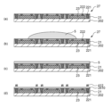
- FIG. 1 is a vertical cross-sectional view showing an example of the configuration of an electronic device.
- FIG. 2 is a partially enlarged view of the area surrounded by the chain line in FIG. 2 is a process diagram showing a method for manufacturing the electronic device shown in FIG. 1.
- FIG. 2 is a diagram for explaining a method of manufacturing the electronic device shown in FIG. 1.
- FIG. 2 is a diagram for explaining a method of manufacturing the electronic device shown in FIG. 1.
- FIG. 2 is a diagram for explaining a method of manufacturing the electronic device shown in FIG. 1.
- FIG. 1 is a vertical cross-sectional view showing an example of the configuration of an electronic device.
- FIG. 2 is a partially enlarged view of the area surrounded by the chain line in FIG. 2 is a process diagram showing a method for manufacturing the electronic device shown in FIG. 1.
- FIG. 2 is a diagram for explaining a method of manufacturing the electronic device shown in FIG. 1.
- FIG. 2 is a diagram for explaining a method of manufacturing the electronic device shown in FIG
- the photosensitive resin composition of the present embodiment contains a polyimide (A) having an imide ring structure in the molecule and a photosensitizer (B), and has a
- the water content is configured to be 0.30% by mass or more and 10% by mass or less.
- the adhesion between the resin film made of the photosensitive resin composition and the copper base material (90° peel It has been found that copper adhesion stability can be improved because manufacturing variations in strength) can be suppressed.
- the detailed mechanism is not clear, it is possible that if the composition contains more than a predetermined amount of water, the performance of the composition will deviate from the predetermined range when storage environmental conditions such as humidity change. It is estimated that it can be suppressed.
- the photosensitive resin composition contains a silane coupling agent, the state of silanization is considered to be stable even if the humidity environment changes.
- polyimide (A) having an imide ring structure in a photosensitive resin composition containing a predetermined amount of water or more, it is possible to suppress fluctuations in the viscosity of the photosensitive resin composition after storage, thereby improving storage stability. It turns out that it can be improved. Further, it is also possible to suppress reduction in elongation of the resin film made of the photosensitive resin composition. On the other hand, by keeping the water content in the photosensitive resin composition below the upper limit above, it is possible to suppress the appearance of the photosensitive resin composition from deteriorating over time immediately after adjustment, and therefore improve storage stability. found.
- the lower limit of the water content in the photosensitive resin composition measured by the Karl Fischer method is 0.30% by mass or more, preferably 0.5% by mass or more, and more preferably 0.6% by mass or more. Thereby, the number of 90° peel strength fluctuations can be reduced and the copper adhesion stability can be improved. Further, the lower limit of the water content in the photosensitive resin composition measured by the Karl Fischer method is more preferably 1.0% by mass or more, and even more preferably The content is 1.5% by mass or more, more preferably 1.8% by mass or more, even more preferably 2.0% by mass or more, even more preferably 2.3% by mass or more, even more preferably 2.5% by mass or more.
- the upper limit of the water content in the photosensitive resin composition is 10% by mass or less, preferably 6% by mass or less, and more preferably 5% by mass or less.
- the amount of water in the photosensitive resin composition measured by the Karl Fischer method further improves storage stability and copper adhesion stability, while preventing the occurrence of turbidity and precipitation in the varnish-like photosensitive resin composition.
- the water content measured by the Karl Fischer method is stable during storage.
- the water content measured by the Karl Fischer method is stable during storage.
- the amount is 0 parts by weight or less, more preferably 28.0 parts by weight or less, even more preferably 24.0 parts by weight or less, even more preferably 20.0 parts by weight or less, even more preferably 18.0 parts by weight or less.
- examples of methods for measuring the water content in the photosensitive resin composition include the following method.
- the mass of water generated from the photosensitive resin composition ( mg) is measured according to the volumetric titration method specified in JIS K 0113:2005.
- the water content is determined when the total amount of the photosensitive resin composition (varnish or solid content) is 100% by mass, and is defined as the water content (mass%).
- the photosensitive resin composition of this embodiment can be used as a negative photosensitive resin composition.
- a resin film (cured film) made of the photosensitive resin composition is obtained.
- the photosensitive resin composition of this embodiment is preferably used for forming a permanent film, a protective film, an insulating film, and a rewiring material in an electronic device.
- electronic equipment refers to semiconductor chips, semiconductor elements, printed wiring boards, electric circuits, display devices such as television receivers and monitors, information and communication terminals, light emitting diodes, physical batteries, chemical batteries, etc. Refers to elements, devices, final products, and other electrical equipment that apply technology.
- the photosensitive resin composition of this embodiment is also applicable to the production of optical waveguides. Specifically, the photosensitive resin composition of this embodiment can be applied to the formation of a core layer and/or a cladding layer of an optical waveguide. It is preferable to apply the method to a pattern forming method using a developer. The use of an organic solvent developer as the developer will be described in detail later.
- the photosensitive resin composition of this embodiment contains polyimide (A) having an imide ring structure in the molecule.
- Polyimide (A) having an imide ring structure in the molecule Polyimide (A) having an imide ring structure in the molecule)
- Polyimide having an imide ring structure (hereinafter sometimes simply referred to as "polyimide”) has an azole structure.
- the photosensitive resin composition of this embodiment can contain one or more polyimides.
- the imide cyclization rate is expressed as ⁇ IM/(IM+AM) ⁇ 100(%) is preferably 90% or more, more preferably 95% or more, even more preferably 98% or more.
- the polyimide resin has no or little amide structure and many imide ring structures.
- the imide cyclization rate can be determined, for example, from the area of a peak corresponding to an amide group or the area of a peak corresponding to an imide ring group in an NMR spectrum.
- the imide cyclization rate can be determined from the area of a peak corresponding to an amide group or the area of a peak corresponding to an imide ring group in an infrared absorption spectrum.
- the 1 H-NMR spectrum of the polyimide (A) of the present embodiment is measured, and in the measured 1 H-NMR spectrum, the area of the peak corresponding to the amide group is defined as A AM and the imide ring group.
- the imide cyclization rate can be determined by the calculation formula ⁇ A IM /(A IM +A AM ) ⁇ 100(%).
- the imide cyclization rate is also referred to as "imidization rate.”
- the azole structure may be present in the side chain of the polyimide, or may be present at the end.
- the polyimide preferably has an azole structure at least at one end.
- Polyimide may have an azole structure at both ends, or may have an azole structure only at one end.
- Preferred azole structures include triazole structures and tetrazole structures.
- triazole structures There are two types of triazole structures: a 1,2,3-triazole structure and a 1,2,4-triazole structure in which the nitrogen atom is located at a different position. Either triazole structure can be used in this embodiment.
- the triazole structure examples include monovalent groups obtained by removing hydrogen atoms from the triazole compounds listed below. However, from the viewpoint of particularly good copper adhesion in this embodiment, the triazole structure is preferably a triazole structure that does not contain a benzene ring skeleton.
- Triazole benzotriazole, tolyltriazole (benzotriazole with a methyl group substituted on the benzene ring, carboxybenzotriazole, 4,5,6,7-tetrahydrobenzotriazole, 4,5,6,7-tetrahydrobenzotriazole, 2- (2'-hydroxy-5'-methylphenyl)benzotriazole, 2-(2'-hydroxy-5'-tert-butylphenyl)benzotriazole, 2-(2'-hydroxy-3'5'-di-tert -butylphenyl)benzotriazole, 2-(2'-hydroxy-4-octoxyphenyl)benzotriazole, etc.
- Examples of the tetrazole structure include monovalent groups obtained by removing hydrogen atoms from the following tetrazole compounds. 1,2,3,4-tetrazole, 5-amino-1,2,3,4-tetrazole, 5-methyl-1,2,3,4-tetrazole, 1H-tetrazole-5-acetic acid, 1H-tetrazole- 5-Succinic acid.
- the azole structure can include a structure represented by the following general formula (AZ).
- "*" represents a bond with polyimide.
- R is a hydrogen atom, a halogen atom, a substituted or unsubstituted alkyl group having 1 to 20 carbon atoms, a substituted or unsubstituted cycloalkyl group having 3 to 15 carbon atoms, or a substituted or unsubstituted cycloalkyl group having 6 to 20 carbon atoms.
- the alkyl group of R may be linear or branched.
- linear alkyl groups include methyl group, ethyl group, propyl group, butyl group, pentyl group, hexyl group, heptyl group, octyl group, nonyl group, decanyl group, undecyl group, dodecyl group, tridecyl group, isotridecyl group, Examples include a tetradecyl group, a pentadecyl group, a hexadecyl group, an isohexadecyl group, a heptadecyl group, an octadecyl group, a nonadecyl group, an icosyl group, an icosyl group, a docosyl group, and the like.
- Examples of branched alkyl groups include 1-methylethyl group, 1-methylpropyl group, 2-methylpropyl group, 1-methylbutyl group, 2-methylbutyl group, 3-methylbutyl group, 1-ethylbutyl group, 2-ethylbutyl group, Examples include 1-methylpentyl group, 2-methylpentyl group, 3-methylpentyl group, and 4-methylpentyl group.
- the cycloalkyl group of R may be monocyclic or polycyclic. Specific examples include cyclopropyl group, cyclobutyl group, cyclopentyl group, cyclohexyl group, cycloheptyl group, cyclooctyl group, and the like.
- Examples of the polycyclic alicyclic group include a norbornyl group, an isobornyl group, a tricyclononyl group, a tricyclodecyl group, and a tetracyclododecyl group.
- Examples of the aromatic hydrocarbon group for R include a phenyl group, a naphthyl group, an anthranyl group, and the like.
- the polyimide of this embodiment may have other functional groups in its side chains.
- the other functional groups are preferably functional groups having 1 to 20 carbon atoms that may contain unsaturated bonds; More preferably, it is a functional group having 1 to 10 carbon atoms.
- the polyimide includes polyimide containing a fluorine atom.
- the present inventors have found that polyimides containing fluorine atoms tend to have better solubility in organic solvents than polyimides containing no fluorine atoms. Therefore, by using polyimide containing a fluorine atom, it is easy to make the photosensitive resin composition have a varnish-like property.
- the amount (mass ratio) of fluorine atoms in the polyimide containing fluorine atoms is, for example, 1 to 30% by mass, preferably 3 to 28% by mass, and more preferably 5 to 25% by mass.
- the amount of fluorine atoms is not too large.
- the polyimide of this embodiment preferably does not contain fluorine atoms.
- the content of fluorine atoms in the polyimide of this embodiment is preferably 0% by mass or more, and preferably 30% by mass when the total amount of polyimide is 100% by mass. % or less, more preferably 20% by mass or less, still more preferably 10% by mass or less, even more preferably 5% by mass or less, even more preferably 3% by mass or less, even more preferably 1% by mass or less, even more preferably 0.5% by mass. % or less, more preferably 0.1% by mass or less.
- the polyimide contains a structural unit represented by the following general formula (a).
- X is a divalent organic group
- Y is a tetravalent organic group
- At least one of X and Y is a fluorine atom-containing group.
- the divalent organic group of X and/or the tetravalent organic group of Y preferably contains an aromatic ring structure, more preferably a benzene ring structure. This tends to further improve heat resistance. From the viewpoint of organic solvent solubility, both X and Y are preferably fluorine atom-containing groups.
- the divalent organic group of X and/or the tetravalent organic group of Y preferably has a structure in which 2 to 6 benzene rings are bonded via a single bond or a divalent linking group. Examples of the divalent linking group here include an alkylene group, a fluorinated alkylene group, and an ether group. The alkylene group and fluorinated alkylene group may be linear or branched.
- the divalent organic group of X has, for example, 6 to 30 carbon atoms.
- the number of carbon atoms in the tetravalent organic group of Y is, for example, 6 to 20. It is preferable that each of the two imide rings in general formula (a) is a 5-membered ring.
- the polyimide contains a structural unit represented by the following general formula (aa).
- Y' represents a single bond or an alkylene group
- X has the same meaning as X in general formula (a).
- the alkylene group of Y' may be linear or branched. It is preferable that some or all of the hydrogen atoms in the alkylene group of Y' are substituted with fluorine atoms.
- the alkylene group of Y' has, for example, 1 to 6 carbon atoms, preferably 1 to 4 carbon atoms, and more preferably 1 to 3 carbon atoms.
- the polyimide of the present embodiment includes a structural unit in which X and Y are organic groups containing no fluorine atom in the structural unit represented by the above-mentioned general formula (a). More preferably, the structural unit represented by the general formula (aa) described above includes a structural unit in which X and Y' are organic groups containing no fluorine atom.
- the polyimide may be soluble or insoluble in the alkaline developer. Whether the polyimide is designed to be soluble in an alkaline developer depends on whether the photosensitive resin composition of this embodiment is applied to development with an alkaline developer or an organic solvent developer.
- the photosensitive resin composition of this embodiment is preferably applied to development using an organic solvent developer.
- the polyimide is substantially insoluble in an alkaline developer.
- the polyimide preferably has no or only a small amount of alkali-soluble groups such as phenolic hydroxy groups or carboxy groups.
- the proportion of structural units having alkali-soluble groups in the polyimide is preferably 0 to 10 mol%, more preferably 0 to 5 mol%, based on all structural units.
- the ratio of structural units having a phenolic hydroxy group in the polyimide is preferably 0 to 10 mol%, more preferably 0 to 5 mol%, based on all structural units.
- polyimide when polyimide has a structural unit represented by the above-mentioned general formula (a), general formula (aa), or general formula (aa), these structural units are phenolic hydroxyl. It is preferable not to have an alkali-soluble group such as a group or a carboxy group.
- polyimide is produced by: (i) first reacting diamine and acid dianhydride (condensation polymerization) to synthesize polyamide; (ii) then imidizing the polyamide (ring-closing reaction); (iii) It can be obtained by introducing a desired functional group to the polymer terminal as necessary.
- a compound containing an azole structure may be reacted with the diamine and the acid dianhydride, and step (iii) above may not be performed.
- the compound containing an azole structure to be reacted in the above step (i) is an azole compound having an amino group, specifically, in the above general formula (AZ), the part "*" is an amino group or an amino group-containing group.
- azole compounds include azole compounds.
- polyimide is synthesized using this method. For specific reaction conditions, please refer to the Examples below.
- the diamine is incorporated into the polymer as a divalent organic group X in general formula (a).
- the acid dianhydride is incorporated into the polymer as a tetravalent organic group Y in general formula (a).
- one or more diamines can be used, and one or more acid dianhydrides can be used.
- raw material diamine examples include 3,4'-diaminodiphenyl ether (3,4'-ODA), 4,4'-diamino-2,2'-bis(trifluoromethyl)biphenyl (TFMB), 3,3 ',5,5'-tetramethylbenzidine, 2,3,5,6-tetramethyl-1,4-phenylenediamine, 3,3'-diaminodiphenylsulfone, 3,3'dimethylbenzidine, 3,3'- Bis(trifluoromethyl)benzidine, 2,2'-bis(p-aminophenyl)hexafluoropropane, bis(trifluoromethoxy)benzidine (TFMOB), 2,2'-bis(pentafluoroethoxy)benzidine (TFEOB) , 2,2'-trifluoromethyl-4,4'-oxydianiline (OBABTF), 2-phenyl-2-trifluoromethyl-bis(p-aminophenyl)methane
- diamines are not limited to these.
- One or more types of diamine can be used.
- the diamines used in the synthesis of the polyimide of this embodiment are preferably 2,2'-bis(trifluoromethyl)benzidine and 4,4 from the viewpoint of further improving storage stability and copper adhesion stability. It contains one or more selected from the group consisting of '-diamino-3,3'-diethyl-5,5'-dimethyldiphenylmethane.
- raw acid dianhydrides include pyromellitic anhydride (PMDA), diphenyl ether-3,3',4,4'-tetracarboxylic dianhydride (ODPA), benzophenone-3,3', 4,4'-tetracarboxylic dianhydride (BTDA), biphenyl-3,3',4,4'-tetracarboxylic dianhydride (BPDA), diphenylsulfone-3,3',4,4'- Tetracarboxylic dianhydride (DSDA), diphenylmethane-3,3',4,4'-tetracarboxylic dianhydride, 2,2-bis(3,4-phthalic anhydride)propane, 2,2-bis (3,4-phthalic anhydride)-1,1,1,3,3,3-hexafluoropropane (6FDA), 4,4'-(hexafluoroisopropylidene)diphthalic anhydride, 4,4'- Oxydiphthalic dian
- the acid dianhydride used in the synthesis of the polyimide of this embodiment is preferably 4,4'-(hexafluoroisopropylidene) diphthalic acid from the viewpoint of further improving storage stability and copper adhesion stability.
- the ratio of diamine and acid dianhydride used is basically 1:1 in molar ratio. However, one may be used in excess in order to obtain a desired terminal structure. Specifically, by using an excessive amount of diamine, the ends (both ends) of the polyimide tend to become amino groups. On the other hand, by using an excessive amount of acid dianhydride, the ends (both ends) of the polyimide tend to become acid anhydride groups. If a polyimide having an acid anhydride group at the end is obtained in the reaction system and an azole compound having an amino group is reacted with the acid anhydride group, a polyimide having an azole structure at the end is obtained.
- terminal amino groups and/or acid anhydride groups of the polyimide obtained by condensation polymerization may be reacted with some reagent so that the polyimide terminals have a desired functional group.
- the weight average molecular weight of the polyimide is, for example, 5,000 to 100,000, preferably 7,000 to 75,000, and more preferably 10,000 to 50,000.
- the weight average molecular weight of the polyimide is high to a certain extent, sufficient heat resistance of the cured film can be obtained, for example.
- the weight average molecular weight of the polyimide is not too large, it becomes easier to dissolve the polyimide in an organic solvent.
- the weight average molecular weight can usually be determined by gel permeation chromatography (GPC) using polystyrene as a standard substance.
- the polystyrene equivalent value was determined from a standard polystyrene calibration curve obtained by GPC (Gel Permeation Chromatography) measurement using THF as a solvent, measurement temperature of 40 ° C., and sample concentration of 0.5 wt%.
- GPC Gel Permeation Chromatography
- the weight average molecular weight of the polyimide of this embodiment is preferably 27,000 or more, more preferably 30,000 or more, still more preferably 33,000 or more, and even more preferably 35,000 or more, more preferably 37,000 or more, even more preferably 40,000 or more, even more preferably 50,000 or more, even more preferably 60,000 or more, even more preferably 70,000 or more, and preferably 200,000 or less, more preferably 150,000 or less, even more preferably is 120,000 or less, more preferably 100,000 or less, even more preferably 90,000 or less.
- the content of polyimide in this embodiment is preferably 5% by mass or more when the total amount of the photosensitive resin composition (varnish) is 100% by mass from the viewpoint of further improving storage stability and copper adhesion stability. , more preferably 8% by mass or more, further preferably 10% by mass or more, still more preferably 12% by mass or more, still more preferably 14% by mass or more, still more preferably 15% by mass or more, and preferably 50% by mass.
- the content is more preferably 40% by mass or less, further preferably 30% by mass or less, still more preferably 25% by mass or less, still more preferably 22% by mass or less, even more preferably 20% by mass or less.
- the photosensitive resin composition of this embodiment contains a photosensitizer.
- the photosensitizer is not particularly limited as long as it is capable of curing the photosensitive resin composition by generating active species when exposed to light.
- the photosensitizer preferably contains a photoradical generator.
- Photoradical generators are particularly effective in polymerizing polyfunctional (meth)acrylate compounds.
- the photoradical generator that can be used is not particularly limited, and known ones can be used as appropriate.
- photosensitizer When using a photosensitizer, only one photosensitizer or two or more photosensitizers may be used.
- the content of the photosensitizer is, for example, 1 to 30 parts by weight, preferably 5 to 20 parts by weight, based on 100 parts by weight of the polyfunctional (meth)acrylate compound.
- the photosensitive resin composition of this embodiment may also contain a silane coupling agent (C).
- a silane coupling agent When using a silane coupling agent, only one silane coupling agent may be used, or two or more silane coupling agents may be used. By using a silane coupling agent, it is possible to further improve the adhesion between the resin film formed from the photosensitive resin composition and the base material.
- silane coupling agent examples include an amino group-containing silane coupling agent, an epoxy group-containing silane coupling agent, a (meth)acryloyl group-containing silane coupling agent, a mercapto group-containing silane coupling agent, and a vinyl group-containing silane coupling agent.
- a silane coupling agent such as the following can be used.
- a silane coupling agent having a cyclic anhydride structure and/or a silane coupling agent having a structure in which a part of the structure derived from an acid anhydride group is ring-opened is used.
- the details are unknown, it is presumed that the cyclic anhydride structure and/or carboxylic acid structure easily reacts with the main chain, side chain, and/or terminal of polyimide, and therefore a particularly good adhesion-improving effect can be obtained.
- the amount of silane coupling agent (C) used in the photosensitive resin composition is, for example, 0.1 to 20 parts by mass, preferably 0.5 to 10 parts by mass, when the amount of polyimide (A) used is 100 parts by mass. Parts by weight, more preferably 1 to 8 parts by weight.
- the photosensitive resin composition of this embodiment preferably contains a polyfunctional (meth)acrylic compound.
- a polyfunctional (meth)acrylic compound refers to a compound in which the number of (meth)acryloyl groups in one molecule is 2 or more. It is thought that the polyfunctional (meth)acrylic compound forms a network structure that "wraps" the polyimide skeleton through polymerization. It is presumed that the performance of the resin film is improved by forming such a complex intertwined structure.
- a polyfunctional (meth)acrylic compound represented by the following general formula can be used as an example of the polyfunctional (meth)acrylic compound.
- R' is a hydrogen atom or a methyl group
- n is 0 to 3
- R is a hydrogen atom or a (meth)acryloyl group.
- polyfunctional (meth)acrylic compounds include the following. Of course, polyfunctional (meth)acrylic compounds are not limited to these.
- Urethane (meth)acrylate, etc. obtained by reaction of hydroxyl group-containing (meth)acrylate such as hydroxyethyl (meth)acrylate.
- the polyfunctional (meth)acrylic compound of the present embodiment preferably contains polyol polyacrylates, more preferably dipentaerythritol polyacrylate and Contains one or more selected from the group consisting of 1,6-hexanediol diacrylate.
- Aronix M-400, Aronix M-460, Aronix M-402, Aronix M-510, Aronix M-520 (manufactured by Toagosei), KAYARAD T-1420, KAYARAD DPHA, KAYARAD DPCA20, KAYARAD DPCA30, KAYAR AD DPCA60, KAYARAD DPCA120 (manufactured by Nippon Kayaku Co., Ltd.), Viscoat #230, Viscoat #300, Viscoat #802, Viscoat #2500, Viscoat #1000, Viscoat #1080 (manufactured by Osaka Organic Chemical Industry Co., Ltd.), NK Ester A-BPE-10, NK Ester Commercial products such as A-GLY-9E, NK Ester A-9550, and NK Ester A-DPH (manufactured by Shin-Nakamura Chemical Industry Co., Ltd.).
- the amount of the polyfunctional (meth)acrylate compound relative to 100 parts by mass of polyimide is preferably 1 to 150 parts by mass, more preferably 20 to 120 parts by mass, and even more preferably 50 to 100 parts by mass. Part by mass.
- the photosensitive resin composition contains a polyfunctional (meth)acrylate compound
- it may contain only one polyfunctional (meth)acrylate compound, or it may contain two or more polyfunctional (meth)acrylate compounds.
- it is preferable to use polyfunctional (meth)acrylate compounds having different numbers of functional groups together. It is thought that by using polyfunctional (meth)acrylate compounds with different numbers of functional groups in combination, a more complex "entangled structure" can be created, further improving the properties of the cured film.
- polyfunctional (meth)acrylate compounds there are also mixtures of polyfunctional (meth)acrylate compounds having different numbers of functional groups.
- polyimide and a polyfunctional (meth)acrylic compound when polyimide and a polyfunctional (meth)acrylic compound are used together, a polymerization reaction of the polyfunctional (meth)acrylic compound can be employed as the curing mechanism. Since this polymerization reaction does not involve dehydration in principle, the combination of polyimide and a polyfunctional (meth)acrylic compound is advantageous in that shrinkage due to heating is small.
- the photosensitive resin composition of this embodiment may also contain a thermal radical initiator.
- a thermal radical initiator accelerates the polymerization reaction of the polyfunctional (meth)acrylic compound, improving the heat resistance of the cured film. and/or the chemical resistance (resistance to organic solvents, etc.) of the cured film can be improved.
- the thermal radical initiator preferably contains an organic peroxide.
- organic peroxides include octanoyl peroxide, lauroyl peroxide, stearoyl peroxide, 1,1,3,3-tetramethylbutylperoxy 2-ethylhexanoate, oxalic acid peroxide, 2,5-dimethyl- 2,5-di(2-ethylhexanoylperoxy)hexane, 1-cyclohexyl-1-methylethylperoxy 2-ethylhexanoate, t-hexylperoxy 2-ethylhexanoate, t-butylperoxy 2-Ethylhexanoate, m-toluyl peroxide, benzoyl peroxide, benzoyl peroxide, methyl ethyl ketone peroxide, acetyl peroxide, t-butyl hydroperoxide, di-t-butyl per
- thermal radical initiator When using a thermal radical initiator, only one thermal radical initiator or two or more thermal radical initiators may be used. When a thermal radical initiator is used, the amount thereof is preferably 0.1 to 30 parts by weight, more preferably 1 to 20 parts by weight, based on 100 parts by weight of the polyfunctional (meth)acrylic compound.
- the photosensitive resin composition of this embodiment may also contain an epoxy compound. It is thought that epoxy compounds form chemical bonds by reacting with polyimide or by reacting with each other. The bonds formed in this way can improve the mechanical properties (tensile elongation, etc.) of the cured film.
- the epoxy compound is not particularly limited as long as it is a compound having an epoxy group in its molecule.
- a specific example of the epoxy compound is an epoxy resin.
- epoxy resins include the following. Of course, epoxy resins are not limited to these. Bisphenol A epoxy resin, bisphenol F epoxy resin, bisphenol E epoxy resin, bisphenol S epoxy resin, hydrogenated bisphenol A epoxy resin, bisphenol M epoxy resin (4,4'-(1,3-phenylenedi) (isopridiene) bisphenol type epoxy resin), bisphenol P type epoxy resin (4,4'-(1,4-phenylene diisopridiene) bisphenol type epoxy resin), bisphenol Z type epoxy resin (4,4'-cyclohexyl Bisphenol-type epoxy resins such as bisphenol-type epoxy resin), tetramethylbisphenol-F-type epoxy resin; phenol novolac-type epoxy resin, brominated phenol novolak-type epoxy resin, cresol novolak-type epoxy resin, tetraphenol-based ethane-type novolac-type epoxy resin, novolac type epoxy resin such as novolac type epoxy resin having a condensed ring aromatic hydro
- the epoxy resin can include a trifunctional or higher polyfunctional epoxy resin (that is, one having three or more epoxy groups in one molecule).
- a trifunctional or higher polyfunctional epoxy resin that is, one having three or more epoxy groups in one molecule.
- the polyfunctional epoxy resin those having 3 or more functionalities and 20 or less functionalities are more preferable.
- examples of the epoxy compound include compounds each having one or more epoxy-containing groups and one or more (meth)acryloyl groups in one molecule. This compound preferably has one epoxy-containing group at one end of the molecule and one (meth)acryloyl group at the other end. Specific examples include glycidyl (meth)acrylate, 4-hydroxybutyl acrylate glycidyl ether, and 3,4-epoxycyclohexylmethyl methacrylate.
- the epoxy compound of this embodiment preferably includes a compound having one or more epoxy-containing groups and one or more (meth)acryloyl groups in one molecule, and more preferably Contains 4-hydroxybutyl acrylate glycidyl ether.
- an epoxy compound When using an epoxy compound, only one epoxy compound may be used, or two or more epoxy compounds may be used in combination.
- the amount thereof is, for example, 0.5 to 100 parts by weight, preferably 1 to 50 parts by weight, and more preferably 3 to 20 parts by weight, based on 100 parts by weight of polyimide.
- the photosensitive resin composition of this embodiment may also contain a curing catalyst.
- a curing catalyst When the photosensitive resin composition contains an epoxy compound, by using a curing catalyst, the polymerization reaction of the epoxy compound is promoted, and for example, the tensile elongation rate of the cured film can be further improved.
- curing catalyst examples include compounds generally known as curing catalysts (often also called curing accelerators) for epoxy resins.
- curing catalysts for example, diazabicycloalkenes and their derivatives such as 1,8-diazabicyclo[5,4,0]undecene-7; amine compounds such as tributylamine and benzyldimethylamine; imidazole compounds such as 2-methylimidazole; triphenyl Organic phosphines such as phosphine and methyldiphenylphosphine; tetraphenylphosphonium/tetraphenylborate, tetraphenylphosphonium/tetrabenzoic acid borate, tetraphenylphosphonium/tetranaphthoic acid borate, tetraphenylphosphonium/tetranaphthoyloxyborate, tetraphenyl Tetra-substituted phosphonium salts such as phosphon
- a curing catalyst When using a curing catalyst, only one curing catalyst may be used, or two or more curing catalysts may be used. When a curing catalyst is used, the amount thereof is, for example, 1 to 80 parts by weight, preferably 5 to 50 parts by weight, and more preferably 5 to 30 parts by weight, based on 100 parts by weight of the epoxy compound.
- the photosensitive resin composition of this embodiment preferably contains an adhesive from the viewpoint of further improving copper adhesion stability.
- the adhesive of this embodiment is, for example, 3-mercapto-1,2,4-triazole, 5-mercapto-4H-1,2,4-triazol-3-ol, 5-mercapto-4-methyl-1, 2,4-triazol-3-ol, 3-methylthio-4H-1,2,4-triazole, 3-methylthio-4-methyl-1,2,4-triazole, 3-mercapto-4-methyl-4H- From the group consisting of 1,2,4-triazole, 3-methylthio-4H-1,2,4-triazole, 5-mercapto-1H-tetrazole, 5-mercapto-1-methyltetrazole, 5-methylthio-1H-tetrazole One or more selected types may be included.
- the adhesive of the present embodiment preferably contains 3-mercapto-1,2,4-triazole from the viewpoint of further improving copper adhesion stability.
- the adhesive of this embodiment is reacted with the epoxy compound of this embodiment dissolved in a solvent at a temperature of 40°C or more and 100°C or less for 1 hour or more and 10 hours or less, It is preferable to prepare a solution of 5% or more and 50% or less and then mix it with other components.
- the content of the adhesive agent (solid content) of this embodiment is preferably 1 part by mass or more, more preferably 2 parts by mass or more, and The amount is preferably 3 parts by mass or more, and preferably 10 parts by mass or less, more preferably 7 parts by mass or less, and still more preferably 5 parts by mass or less.
- the photosensitive resin composition of this embodiment preferably contains a solvent. Thereby, a photosensitive resin film can be easily formed on a base material (particularly a base material having steps) by a coating method.
- the solvent usually includes an organic solvent.
- the organic solvent is not particularly limited as long as it can dissolve or disperse each of the above-mentioned components and does not substantially chemically react with each component.
- organic solvents examples include acetone, methyl ethyl ketone, toluene, propylene glycol methyl ethyl ether, propylene glycol dimethyl ether, propylene glycol 1-monomethyl ether 2-acetate, diethylene glycol ethyl methyl ether, diethylene glycol monoethyl ether acetate, diethylene glycol monobutyl ether acetate, and benzyl.
- the organic solvent of the present embodiment preferably contains one or more selected from the group consisting of ethyl lactate and ⁇ -butyrolactone.
- the photosensitive resin composition of this embodiment contains a solvent
- the photosensitive resin composition of this embodiment is usually varnish-like. Since the photosensitive resin composition of this embodiment is varnish-like, it is possible to form a uniform film by coating. Moreover, it is preferable that the photosensitive resin composition of this embodiment is varnish-like and that at least the polyimide is dissolved in a solvent. As described above, by selecting a polyimide with an appropriate chemical structure, the solvent solubility of the polyimide can be increased.
- the concentration of the total solid content in the photosensitive resin composition is preferably 10 to 50% by mass, more preferably 20% by mass. It is used in an amount of ⁇ 45% by mass. By setting it as this range, each component can be fully dissolved or dispersed. In addition, good coating properties can be ensured, which in turn leads to improved flatness during spin coating. Furthermore, by adjusting the content of nonvolatile components, the viscosity of the photosensitive resin composition can be appropriately controlled.
- the photosensitive resin composition of this embodiment may contain components other than the above-mentioned components, if necessary.
- examples of such components include surfactants, antioxidants, fillers such as silica, sensitizers, film-forming agents, and the like.
- the lower limit of the glass transition temperature of the cured film of the photosensitive resin composition measured by TMA is, for example, 200°C or higher, preferably 230°C or higher, and more preferably 250°C or higher. Thereby, the heat resistance of the cured film can be improved.
- the upper limit of the glass transition temperature of the cured film of the photosensitive resin composition is not particularly limited, but is, for example, 400° C. or lower.
- the appearance of the photosensitive resin composition of the present embodiment after being left at 23° C. for 24 hours is preferably free of precipitation, and more preferably free of precipitation or turbidity.
- the 90 degree peel strength of the photosensitive resin composition measured according to the procedure described in Examples is, for example, 0.9 N/cm or more, preferably 1.0 N/cm or more, more preferably 1.6 N/cm. That's all. This makes it possible to realize a resin film with excellent copper adhesion in actual processes.
- the upper limit of the 90 degree peel strength of the photosensitive resin composition of the present embodiment is not particularly limited, but is, for example, 10.0 N/cm or less, may be 7.0 N/cm or less, and may be 5.0 N/cm or less. It may be less than cm.
- the 90 degree peel strength fluctuation number of the photosensitive resin composition of the present embodiment is preferably 70% or less, more preferably 60% or less, from the viewpoint of further improving copper adhesion stability. % or less, more preferably 50% or less, even more preferably 45% or less, still more preferably 40% or less, even more preferably 35% or less.
- the lower limit of the number of changes in 90 degree peel strength of the photosensitive resin composition of the present embodiment is not particularly limited, but may be, for example, 0% or more, 3% or more, or 5% or more. .
- the viscosity of the photosensitive resin composition is ⁇ 0
- the viscosity of the photosensitive resin composition left standing at 23° C. for 7 days is ⁇ 1 .
- the value of ⁇ 1 / ⁇ 0 is preferably 1.5 or less, more preferably 1.3 or less, even more preferably 1.1 or less.
- the value of ⁇ 1 / ⁇ 0 is 1, but depending on various conditions, it may be less than 1, for example, 0.9.
- the value of ⁇ 1 / ⁇ 0 of the photosensitive resin composition of the present embodiment is more preferably 1.08 or less, still more preferably 1.05 or less, and even more preferably It is 1.03 or less.
- the viscosity in this embodiment is a value obtained by measuring the viscosity of the photosensitive resin composition immediately after blending using an E-type viscometer.
- An example of the method for producing the photosensitive resin composition of the present embodiment includes a step of dissolving polyimide (A) having an imide ring structure in the molecule and a photosensitizer (B) in a solvent to obtain a photosensitive resin composition.
- a step of dissolving polyimide (A) having an imide ring structure in the molecule and a photosensitizer (B) in a solvent to obtain a photosensitive resin composition.
- the water content in the photosensitive resin composition measured by the Karl Fischer method is 0.30% by mass or more and 10% by mass or less (a predetermined range).
- the above-mentioned numerical range can be adopted as the predetermined range of the water content in the photosensitive resin composition.
- the method for adjusting the water content is not particularly limited.
- the method for producing the photosensitive resin composition includes at least one step of measuring the water content in the photosensitive resin composition by the Karl Fischer method and determining that the water content is within a predetermined range. is preferred. If the moisture content is below a predetermined range, water is added to adjust the moisture content.
- the method for producing the photosensitive resin composition includes preparing an aqueous solution containing the silane coupling agent (C) and water during the process of obtaining the photosensitive resin composition, and adding this aqueous solution to the photosensitive resin composition. It may also include a step of.
- the timing of adding the aqueous solution to the photosensitive resin composition is not particularly limited, but it may be before or after adding the above-mentioned component (A) and component (B) to the solvent. It may be added to the solvent.
- the aqueous solution may be added to the solvent once or twice or more.
- the method for manufacturing an electronic device is as follows: a film forming step of forming a photosensitive resin film on the substrate using the above photosensitive resin composition; an exposure step of exposing the photosensitive resin film; a development step of developing the exposed photosensitive resin film; can include. Moreover, it is preferable that the manufacturing method of the electronic device of this embodiment includes the thermosetting process of heating and hardening the exposed photosensitive resin film after the above-mentioned image development process. Thereby, a cured film with sufficient heat resistance can be obtained. In the manner described above, an electronic device including a resin film made of a cured film of the photosensitive resin composition of this embodiment can be manufactured.
- FIG. 1 is a longitudinal cross-sectional view showing an example of an electronic device according to this embodiment.
- FIG. 2 is a partially enlarged view of the area surrounded by the chain line in FIG.
- the upper side in FIG. 1 will be referred to as “upper” and the lower side will be referred to as “lower”.
- the electronic device 1 shown in FIG. 1 has a so-called package-on-package structure including a through electrode substrate 2 and a semiconductor package 3 mounted thereon.
- the through electrode substrate 2 includes an insulating layer 21 , a plurality of through wirings 221 penetrating from the top surface to the bottom surface of the insulating layer 21 , a semiconductor chip 23 embedded inside the insulating layer 21 , and a semiconductor chip 23 provided on the bottom surface of the insulating layer 21 .
- the semiconductor package 3 includes a package substrate 31, a semiconductor chip 32 mounted on the package substrate 31, a bonding wire 33 that electrically connects the semiconductor chip 32 and the package substrate 31, and a semiconductor chip 32 and the bonding wire 33. It includes an embedded sealing layer 34 and solder bumps 35 provided on the lower surface of the package substrate 31.
- a semiconductor package 3 is stacked on the through electrode substrate 2. Thereby, the solder bumps 35 of the semiconductor package 3 and the upper wiring layer 25 of the through electrode substrate 2 are electrically connected.
- the through electrode substrate 2 and the semiconductor package 3, which are equipped with mutually different semiconductor chips, are stacked, the packaging density per unit area can be increased. Therefore, it is possible to achieve both miniaturization and high performance.
- the lower wiring layer 24 and the upper wiring layer 25 included in the through electrode substrate 2 shown in FIG. 2 each include an insulating layer, a wiring layer, a through wiring, and the like.
- the lower wiring layer 24 and the upper wiring layer 25 include wiring inside and on the surface, and are electrically connected to each other via the through wiring 221 that penetrates the insulating layer 21.
- the wiring layer included in the lower wiring layer 24 is connected to the semiconductor chip 23 and the solder bumps 26. Therefore, the lower wiring layer 24 functions as a rewiring layer of the semiconductor chip 23, and the solder bumps 26 function as external terminals of the semiconductor chip 23.
- the through wiring 221 shown in FIG. 2 is provided so as to penetrate through the insulating layer 21, as described above. Thereby, the lower wiring layer 24 and the upper wiring layer 25 are electrically connected, and the through electrode substrate 2 and the semiconductor package 3 can be stacked, so that the electronic device 1 can be highly functional. can.
- the wiring layer 253 included in the upper wiring layer 25 shown in FIG. 2 is connected to the through wiring 221 and the solder bumps 35. Therefore, the upper wiring layer 25 is electrically connected to the semiconductor chip 23 and functions as a rewiring layer for the semiconductor chip 23 and as an interposer interposed between the semiconductor chip 23 and the package substrate 31. also works.
- the cured film of the photosensitive resin composition of this embodiment can be used to constitute the insulating layer of the rewiring layer.
- the semiconductor chip 23 and the rewiring layer (upper wiring layer 25) provided on the surface of the semiconductor chip 23 are provided, and the insulating layer in the rewiring layer is the photosensitive layer of the present embodiment. It is possible to realize an electronic device composed of a cured product of a polyurethane resin composition.
- the effect of reinforcing the insulating layer 21 can be obtained. Therefore, even if the lower wiring layer 24 and the upper wiring layer 25 have low mechanical strength, the mechanical strength of the through electrode substrate 2 as a whole can be prevented from decreasing. As a result, it is possible to further reduce the thickness of the lower wiring layer 24 and the upper wiring layer 25, and it is possible to further reduce the height of the electronic device 1.
- the electronic device 1 shown in FIG. 1 also includes a through wiring 222 provided to penetrate the insulating layer 21 located on the upper surface of the semiconductor chip 23. Thereby, electrical connection between the upper surface of the semiconductor chip 23 and the upper wiring layer 25 can be achieved.
- the insulating layer 21 is provided to cover the semiconductor chip 23. This increases the effect of protecting the semiconductor chip 23. As a result, the reliability of the electronic device 1 can be improved. Moreover, the electronic device 1 can be easily applied to a mounting method such as the package-on-package structure according to the present embodiment.
- the diameter W (see FIG. 2) of the through wiring 221 is not particularly limited, but is preferably about 1 to 100 ⁇ m, more preferably about 2 to 80 ⁇ m. Thereby, the conductivity of the through wiring 221 can be ensured without impairing the mechanical properties of the insulating layer 21.
- the semiconductor package 3 shown in FIG. 1 may be any type of package.
- QFP Quad Flat Package
- SOP Small Outline Package
- BGA Bit Grid Array
- CSP Chip Size Package
- QFN Quadrature Non-leaded Package
- SON Small Outline Non-leaded Package
- forms such as LF-BGA (Lead Flame BGA).
- the arrangement of the semiconductor chips 32 is not particularly limited, but as an example, in FIG. 1, a plurality of semiconductor chips 32 are stacked. As a result, the packaging density is increased. Note that the plurality of semiconductor chips 32 may be arranged side by side in the plane direction, or may be stacked in the thickness direction and arranged side by side in the plane direction.
- the package substrate 31 may be any type of substrate, but may include, for example, an insulating layer, a wiring layer, a through wiring, etc. (not shown). Among these, the solder bumps 35 and the bonding wires 33 can be electrically connected via the through wiring.
- the sealing layer 34 is made of, for example, a known sealing resin material. By providing such a sealing layer 34, the semiconductor chip 32 and bonding wires 33 can be protected from external forces and the external environment.
- the semiconductor chip 23 included in the through electrode substrate 2 and the semiconductor chip 32 included in the semiconductor package 3 are arranged close to each other. This makes it possible to enjoy benefits such as faster mutual communication and lower loss.
- one of the semiconductor chips 23 and 32 is used as an arithmetic element such as a CPU (Central Processing Unit), a GPU (Graphics Processing Unit), or an AP (Application Processor), and the other is used as a D RAM (Dynamic Random Access
- storage elements such as memory (Memory) or flash memory, these elements can be placed close to each other in the same device. Thereby, it is possible to realize an electronic device 1 that is both highly functional and compact.
- FIG. 3 is a process diagram showing a method for manufacturing the electronic device 1 shown in FIG. 1. Further, FIGS. 4 to 6 are diagrams for explaining a method of manufacturing the electronic device 1 shown in FIG. 1, respectively.
- the manufacturing method of the electronic device 1 includes a chip placement step S1 in which the insulating layer 21 is obtained so as to embed the semiconductor chip 23 provided on the substrate 202 and the through wirings 221 and 222, and an upper layer is formed on the insulating layer 21 and the semiconductor chip 23.
- An upper wiring layer forming step S2 for forming the wiring layer 25 a substrate peeling step S3 for peeling off the substrate 202, a lower wiring layer forming step S4 for forming the lower wiring layer 24, forming the solder bumps 26, and forming the through electrode substrate. 2, and a stacking step S6 of stacking the semiconductor package 3 on the through electrode substrate 2.
- a photosensitive resin varnish 5 (varnish-like photosensitive resin composition) is placed on the insulating layer 21 and the semiconductor chip 23, and a first resin is used to form the photosensitive resin layer 2510.
- the process includes a second curing step S28 and a through wiring forming step S29 in which the through wiring 254 is formed in the opening 424 (through hole).
- Chip placement process S1 First, as shown in FIG. 4A, a chip includes a substrate 202, a semiconductor chip 23 and through wirings 221 and 222 provided on the substrate 202, and an insulating layer 21 provided to embed these. An embedded structure 27 is prepared.
- the constituent material of the substrate 202 is not particularly limited, and examples thereof include metal materials, glass materials, ceramic materials, semiconductor materials, organic materials, and the like. Furthermore, the substrate 202 may be a semiconductor wafer such as a silicon wafer, a glass wafer, or the like.
- the semiconductor chip 23 is bonded onto the substrate 202.
- a plurality of semiconductor chips 23 are placed on the same substrate 202 while being spaced apart from each other.
- the plurality of semiconductor chips 23 may be of the same type or may be of different types.
- the substrate 202 and the semiconductor chip 23 may be fixed via an adhesive layer (not shown) such as a die attach film.
- an interposer (not shown) may be provided between the substrate 202 and the semiconductor chip 23.
- the interposer functions as a rewiring layer for the semiconductor chip 23, for example. Therefore, the interposer may include pads (not shown) for electrical connection with electrodes of the semiconductor chip 23, which will be described later. Thereby, the pad spacing and arrangement pattern of the semiconductor chip 23 can be changed, and the degree of freedom in designing the electronic device 1 can be further increased.
- an inorganic substrate such as a silicon substrate, a ceramic substrate, or a glass substrate, an organic substrate such as a resin substrate, etc. are used as the interposer.
- the insulating layer 21 may be, for example, a resin film (organic insulating layer) containing a thermosetting resin or a thermoplastic resin as mentioned as a component of the photosensitive resin composition, or a general sealing layer used in the semiconductor technical field. It may also be a stopper.
- Examples of the constituent material of the through wirings 221 and 222 include copper or a copper alloy, aluminum or an aluminum alloy, gold or a gold alloy, silver or a silver alloy, nickel or a nickel alloy, and the like.
- chip-embedded structure 27 may be prepared using a method different from that described above.
- the application of the photosensitive resin varnish 5 is performed using, for example, a spin coater, a bar coater, a spray device, an inkjet device, or the like.
- the viscosity of the photosensitive resin varnish 5 is not particularly limited, but is 10 cP to 6000 cP, preferably 20 cP to 5000 cP, and more preferably 30 cP to 4000 cP.
- a thinner photosensitive resin layer 2510 (see FIG. 4(d)) can be formed.
- the upper wiring layer 25 can be made thinner, making it easier to make the electronic device 1 thinner.
- the viscosity of the photosensitive resin varnish 5 is, for example, a value measured using a cone-plate viscometer (TV-25, manufactured by Toki Sangyo Co., Ltd.) at a rotation speed of 100 rpm.
- the drying conditions for the photosensitive resin varnish 5 are not particularly limited, but include, for example, heating at a temperature of 80 to 150° C. for 1 to 60 minutes.
- the photosensitive resin film is a photosensitive resin composition of this embodiment, and is a resin film having photosensitivity.
- the photosensitive resin film is manufactured, for example, by applying the photosensitive resin varnish 5 onto a base such as a carrier film using various coating devices, and then drying the resulting coating film.
- the photosensitive resin layer 2510 is subjected to pre-exposure heat treatment, if necessary.
- pre-exposure heat treatment By performing the pre-exposure heat treatment, the molecules contained in the photosensitive resin layer 2510 are stabilized, and the reaction in the first exposure step S21 described later can be stabilized.
- the adverse effects of heating on the photoacid generator can be minimized.
- the temperature of the pre-exposure heat treatment is preferably 70 to 130°C, more preferably 75 to 120°C, and even more preferably 80 to 110°C. If the temperature of the pre-exposure heat treatment is below the lower limit, there is a possibility that the purpose of stabilizing molecules by the pre-exposure heat treatment will not be achieved. On the other hand, if the temperature of the pre-exposure heat treatment exceeds the upper limit, the movement of the photoacid generator becomes too active, resulting in the effect that it becomes difficult to generate acid even when light is irradiated in the first exposure step S21, which will be described later. There is a possibility that the patterning accuracy will decrease due to the wide range of patterning.
- the time of the pre-exposure heat treatment is appropriately set depending on the temperature of the pre-exposure heat treatment, but at the above temperature it is preferably 1 to 10 minutes, more preferably 2 to 8 minutes, still more preferably 3 to 8 minutes. It is said to be 6 minutes. If the time for the pre-exposure heat treatment is less than the lower limit, the heating time will be insufficient, and there is a risk that the purpose of the pre-exposure heat treatment, which is stabilization of molecules, will not be achieved. On the other hand, if the pre-exposure heat treatment time exceeds the above upper limit, the heating time will be too long and the action of the photoacid generator will be inhibited even if the pre-exposure heat treatment temperature is within the above range. There is a risk of it getting lost.
- the atmosphere for the heat treatment is not particularly limited. Although an inert gas atmosphere, a reducing gas atmosphere, etc. may be used, in consideration of work efficiency, etc., it is preferable to use the atmosphere.
- the atmospheric pressure is not particularly limited. It may be under reduced pressure or increased pressure, but in consideration of work efficiency etc., normal pressure is used. Note that normal pressure refers to a pressure of about 30 to 150 kPa, preferably atmospheric pressure.
- a mask 412 is placed in a predetermined area on the photosensitive resin layer 2510. Then, light (active radiation) is irradiated through the mask 412. Thereby, exposure processing is performed on the photosensitive resin layer 2510 according to the pattern of the mask 412.
- FIG. 4(d) shows a case where the photosensitive resin layer 2510 has so-called negative photosensitivity.
- a region of the photosensitive resin layer 2510 corresponding to the light-blocking portion of the mask 412 is dissolved in the developer.
- active chemical species are generated from the photocationic polymerization initiator.
- the active species acts as a catalyst for the curing reaction.
- the amount of exposure in the exposure process is not particularly limited. 100 to 2000 mJ/cm 2 is preferable, and 200 to 1000 mJ/cm 2 is more preferable. Thereby, underexposure and overexposure in the photosensitive resin layer 2510 can be suppressed. As a result, high patterning accuracy can finally be achieved. Thereafter, if necessary, the photosensitive resin layer 2510 is subjected to post-exposure heat treatment.
- the temperature of the post-exposure heat treatment is not particularly limited.
- the temperature is preferably 50 to 150°C, more preferably 50 to 130°C, even more preferably 55 to 120°C, particularly preferably 60 to 110°C.
- the time for the post-exposure heat treatment is appropriately set depending on the temperature of the post-exposure heat treatment.
- the heating time is preferably 1 to 30 minutes, more preferably 2 to 20 minutes, and even more preferably 3 to 15 minutes.
- the atmosphere for the post-exposure heat treatment is not particularly limited. Although an inert gas atmosphere, a reducing gas atmosphere, etc. may be used, in consideration of work efficiency, etc., it is preferable to use the atmosphere.
- the atmospheric pressure of the post-exposure heat treatment is not particularly limited. It may be under reduced pressure or increased pressure, but in consideration of work efficiency etc., normal pressure is used. Thereby, the pre-exposure heat treatment can be performed relatively easily.
- normal pressure refers to a pressure of about 30 to 150 kPa, preferably atmospheric pressure.
- the developer examples include an organic solvent developer, a water-soluble developer, and the like.
- the developer preferably contains an organic solvent. More specifically, the developer is preferably a developer containing an organic solvent as a main component (a developer in which 95% by mass or more of the components is an organic solvent). By developing with a developer containing an organic solvent, swelling of the pattern due to the developer can be suppressed more than when developing with an alkaline developer (aqueous). In other words, it is easier to obtain a finer pattern.
- organic solvents that can be used in the developer include ketone solvents such as cyclopentanone, ester solvents such as propylene glycol monomethyl ether acetate (PGMEA) and butyl acetate, ether solvents such as propylene glycol monomethyl ether, etc.
- an organic solvent developer may be used, which consists only of an organic solvent and does not contain any impurities other than unavoidable impurities. Impurities that are unavoidably included include metal elements and water, but from the viewpoint of preventing contamination of electronic devices, it is better to have fewer impurities that are unavoidably included.
- the method of bringing the developer into contact with the photosensitive resin layer 2510 is not particularly limited. Generally known methods such as a dipping method, a paddle method, and a spray method can be applied as appropriate.
- the time for the development step is usually about 5 to 300 seconds, preferably about 10 to 120 seconds, and is adjusted as appropriate based on the thickness of the resin film, the shape of the pattern to be formed, etc.
- the photosensitive resin layer 2510 is subjected to a curing process (post-development heat treatment).
- the conditions of the curing treatment are not particularly limited, but the heating temperature is about 160 to 250° C. and the heating time is about 30 to 240 minutes. Thereby, the photosensitive resin layer 2510 can be cured and the organic insulating layer 251 can be obtained while suppressing the thermal influence on the semiconductor chip 23.
- Wiring layer forming step S24 Next, a wiring layer 253 is formed on the organic insulating layer 251 (see FIG. 5(f)).
- the wiring layer 253 is formed by obtaining a metal layer using a vapor phase film forming method such as a sputtering method or a vacuum evaporation method, and then patterning the metal layer using a photolithography method and an etching method. Prior to forming the wiring layer 253, surface modification treatment such as plasma treatment may be performed.
- a photosensitive resin layer 2520 is obtained in the same manner as in the first resin film arrangement step S20.
- the photosensitive resin layer 2520 is arranged to cover the wiring layer 253. Thereafter, if necessary, the photosensitive resin layer 2520 is subjected to pre-exposure heat treatment.
- the processing conditions are, for example, the conditions described in the first resin film placement step S20.
- Second exposure step S26 Next, the photosensitive resin layer 2520 is exposed to light.
- the processing conditions are, for example, the conditions described in the first exposure step S21. Thereafter, the photosensitive resin layer 2520 is subjected to post-exposure heat treatment, if necessary.
- the processing conditions are, for example, the conditions described in the first exposure step S21.
- Second development step S27 the photosensitive resin layer 2520 is subjected to a development process.
- the processing conditions are, for example, the conditions described in the first development step S22.
- an opening 424 passing through the photosensitive resin layers 2510 and 2520 is formed (see FIG. 5(h)).
- Second curing step S28 After the development process, the photosensitive resin layer 2520 is subjected to a curing process (post-development heat treatment).
- the curing conditions are, for example, the conditions described in the first curing step S23. Thereby, the photosensitive resin layer 2520 is cured, and an organic insulating layer 252 is obtained (see FIG. 6(i)).
- the upper wiring layer 25 has two layers, the organic insulating layer 251 and the organic insulating layer 252, but it may have three or more layers. In this case, after the second curing step S28, a series of steps from the wiring layer forming step S24 to the second curing step S28 may be repeatedly added.
- a known method is used to form the through wiring 254, and for example, the following method is used.
- a seed layer (not shown) is formed on the organic insulating layer 252.
- the seed layer is formed on the inner surface (side surface and bottom surface) of the opening 424 as well as on the upper surface of the organic insulating layer 252.
- a copper seed layer is used as the seed layer.
- the seed layer is formed by, for example, a sputtering method.
- the seed layer may be made of the same type of metal as the through wiring 254 to be formed, or may be made of a different type of metal.
- a resist layer (not shown) is formed on a region other than the opening 424 of the seed layer (not shown). Then, using this resist layer as a mask, the opening 424 is filled with metal. For example, electrolytic plating is used for this filling. Examples of the metal to be filled include copper or a copper alloy, aluminum or an aluminum alloy, gold or a gold alloy, silver or a silver alloy, nickel or a nickel alloy. In this way, the conductive material is buried in the opening 424, and the through wiring 254 is formed.
- the resist layer (not shown) is removed. Furthermore, the seed layer (not shown) on the organic insulating layer 252 is removed. For this purpose, for example, a flash etching method can be used.
- the location where the through wiring 254 is formed is not limited to the illustrated position.
- Lower wiring layer forming step S4 Next, as shown in FIG. 6(k), a lower wiring layer 24 is formed on the lower surface side of the insulating layer 21.
- the lower wiring layer 24 may be formed by any method, for example, in the same manner as the upper wiring layer forming step S2 described above.
- the lower wiring layer 24 formed in this way is electrically connected to the upper wiring layer 25 via the through wiring 221.
- solder bump forming step S5 As shown in FIG. 6(L), solder bumps 26 are formed on the lower wiring layer 24. Further, a protective film such as a solder resist layer may be formed on the upper wiring layer 25 and the lower wiring layer 24 as necessary. In the manner described above, the through electrode substrate 2 is obtained.
- the through electrode substrate 2 shown in FIG. 6(L) can be divided into a plurality of regions. Therefore, for example, by dividing the through electrode substrate 2 into pieces along the dashed line shown in FIG. 6(L), a plurality of through electrode substrates 2 can be efficiently manufactured. Note that, for example, a diamond cutter or the like can be used to separate the pieces into pieces.
- Such a method of manufacturing the electronic device 1 can be applied to a wafer level process or a panel level process using a large-area substrate. Thereby, manufacturing efficiency of the electronic device 1 can be increased and costs can be reduced.
- the imidization rate of the resin analyzed by 1 H-NMR was 95% or more.
- the weight average molecular weight (Mw) is determined by GPC (Gel Permeation Chromatography) measurement of polyimide resin using THF as a solvent at a measurement temperature of 40°C and a sample concentration of 0.5 wt%, and then by GPC measurement under the same conditions. It was determined using the polystyrene equivalent value calculated from the standard polystyrene (PS) calibration curve obtained by.
- the imidization rate is determined by measuring the 1 H-NMR spectrum of the polyimide resin.
- the area of the peak corresponding to the amide group is A AM
- the area of the peak corresponding to the imide ring group is A AM
- IM it was calculated using the formula ⁇ A IM /(A IM +A AM ) ⁇ 100(%).
- ⁇ Synthesis of polyimide precursor resin (A-4)> Put 428 g of ⁇ -butyrolactone, 155.11 g of 4,4'-oxydiphthalic dianhydride, and 130.14 g of 2-hydroxyethyl methacrylate into a 2 L separable flask, and stir the components in the flask at room temperature to completely dissolve them. Ta. Subsequently, 79.1 g of pyridine was added while stirring at room temperature, and the mixture was further stirred at room temperature for 16 hours.
- Resin (A-4) had a weight average molecular weight (Mw) of 30,000 as measured by GPC. Furthermore, the imidization rate of the resin analyzed by 1 H-NMR was less than 5%.
- the water content (mass%) in the varnish is the water content in the varnish that includes all the water added as raw materials during formulation, the water contained in the silane coupling agent (C-1), and the water mixed during composition preparation.
- the amount is a value measured using a Karl Fischer moisture meter.
- A-1) Polyimide resin having an imide ring structure synthesized above (A-1)
- A-2) Polyimide resin having an imide ring structure synthesized above (A-2)
- A-3) Polyimide resin having an imide ring structure synthesized above (A-3)
- A-4) Polyimide precursor synthesized above ⁇ for comparative example>
- A-5) Polyimide resin having an imide ring structure synthesized above (A-5)
- D-1 NK ester A-9550 (manufactured by Shin Nakamura Chemical Co., Ltd., dipentaerythritol polyacrylate, compound having 5 to 6 acryloyl groups in one molecule)
- D-2) Viscoat #230 (manufactured by Osaka Organic Chemical Industry Co., Ltd., a compound having two acryloyl groups in one molecule)
- G-1 Ethyl lactate (EL)
- G-2 Gamma-butyrolactone (GBL)
- the obtained photosensitive resin composition was evaluated based on the items listed in Table 1. Note that in Table 1, "-" means that no evaluation was performed.
- the mass of water generated from the photosensitive resin composition ( mg) was measured according to the volumetric titration method specified in JIS K 0113:2005. Next, the water content was determined when the total amount of the photosensitive resin composition (varnish) was 100% by mass, and was defined as the water content (mass%).
- ⁇ Adhesion 90 degree peel strength> (Creation of substrate for 90 degree peel strength evaluation)
- the obtained photosensitive resin composition was spin-coated onto a 12-inch silicon wafer having a 3000 ⁇ plated copper layer on its surface to a dry film thickness of 10 ⁇ m, and then coated at 120° C. for 3 minutes.
- a photosensitive resin film was obtained by heating.
- the obtained photosensitive resin film was exposed to 300 mJ/cm 2 using an i-line stepper through a photomask so that a range of 6.5 mm in width and 50 mm in length was exposed.
- the exposed resin film was developed with cyclopentanone and propylene glycol monomethyl ether acetate together with the silicon wafer using a spray developing machine, and then air-dried using a spin dryer and then dried on a hot plate at 120°C for 2 minutes. went. Furthermore, after that, heat treatment was performed at 200° C. for 90 minutes in a nitrogen atmosphere to obtain a cured film. Subsequently, the silicon wafer was cut so that the obtained cured film with a width of 6.5 mm and a length of 50 mm remained, and the end portion (5 mm) of the cured film was immersed in a 2% hydrofluoric acid aqueous solution at 23 ° C. for 6 hours. The substrate was washed with water and dried to obtain a substrate for evaluation of 90 degree peel strength from which the film at the edges was peeled off.
- the unit of 90 degree peel strength is N/cm. A higher 90 degree peel strength is preferable from the viewpoint of reliability.
- the obtained photosensitive resin composition was spin-coated onto a 12-inch silicon wafer with a 3000 ⁇ plated copper layer on the surface to a dry film thickness of 5 ⁇ m, and dried on a hot plate at 120° C. for 3 minutes.
- a photosensitive resin film was obtained.
- the i-line stepper manufactured by CANON, FPA-5500iX ), the i-line was irradiated while changing the exposure amount.
- the exposed film was developed using a spray developer using cyclopentanone at 2500 rpm for 30 seconds, then developed using propylene glycol monomethyl ether acetate at 2500 rpm for 10 seconds, and then spin-dried at 2500 rpm for 10 seconds.
- ⁇ Normal temperature viscosity change rate> The viscosity of the photosensitive resin composition immediately after blending was measured using an E-type viscometer (TVE-25L). The viscosity at this time was designated as A. Thereafter, the varnish of the photosensitive resin composition used to measure the viscosity A was stored at 23° C. for 7 days, and the viscosity was measured again. The viscosity at this time was designated as B. Using the values of viscosity A and viscosity B, "viscosity change rate" was calculated based on the following formula.
- Viscosity change rate [%] ⁇ (viscosity A - viscosity B)/viscosity A ⁇ x 100
- the obtained cured product was cut with a dicing saw along with the silicon wafer to a width of 5 mm, and then peeled off from the substrate by immersing it in a 2% by mass hydrofluoric acid aqueous solution.
- the peeled film was dried at 60° C. for 10 hours to obtain a test piece (30 mm x 5 mm x 10 ⁇ m thick).
- Tg glass transition temperature
- the exposed resin film was developed with cyclopentanone and propylene glycol monomethyl ether acetate together with the silicon wafer using a spray developing machine, and then air-dried using a spin dryer and then dried on a hot plate at 140°C for 2 minutes. went. Furthermore, after that, heat treatment was performed at 200° C. for 120 minutes in a nitrogen atmosphere to obtain a resin film.
- the obtained resin film was peeled from the substrate by immersing it in a 2% by mass hydrofluoric acid aqueous solution, washed with water, and then dried at 60°C for 10 hours to obtain a test piece for measurement (50 mm x 5 mm x 10 ⁇ m thick). .
- the measurement test piece obtained in the above was tested in accordance with JIS K 7161 in an atmosphere of 23°C using a tensile tester (manufactured by Orientech, Tensilon RTC-1210A). A tensile test was conducted in accordance with the method, and the tensile elongation rate of the test piece was measured. The stretching speed in the tensile test was 5 mm/min. The unit of tensile elongation is %.
- the photosensitive resin compositions of Examples 1 to 6 have a smaller room temperature viscosity change rate than Comparative Example 1, and have a better varnish appearance than Comparative Example 3, so they have excellent storage stability. Since the number of 90 degree peel strength fluctuations was smaller than that of Sample No. 2, the result showed that excellent copper adhesion stability was exhibited.
- the photosensitive resin compositions of Examples 7 to 9 have a smaller room-temperature viscosity change rate than Comparative Example 1, and have a better varnish appearance than Comparative Example 3, so they have excellent storage stability. Compared to Comparative Examples 2 and 4, the number of changes in 90 degree peel strength was smaller, indicating excellent copper adhesion stability.
Abstract
This photosensitive resin composition contains a polyimide (A) having an imide ring structure in the molecule, and a photosensitizer (B), and the water content measured by the Karl Fischer method is 0.30-10 mass% inclusive.
Description
本発明は、感光性樹脂組成物、樹脂膜、および電子装置に関する。
The present invention relates to a photosensitive resin composition, a resin film, and an electronic device.
電気・電子分野においては、絶縁層などの硬化膜を形成するために、ポリアミド樹脂および/またはポリイミド樹脂を含む感光性樹脂組成物が用いられることがある。そのため、ポリアミド樹脂および/またはポリイミド樹脂を含む感光性樹脂組成物がこれまで検討されてきている。
特許文献1には、ポリイミド樹脂および光重合開始剤を含む感光性樹脂組成物が記載されている。 In the electrical and electronic fields, photosensitive resin compositions containing polyamide resins and/or polyimide resins are sometimes used to form cured films such as insulating layers. Therefore, photosensitive resin compositions containing polyamide resins and/or polyimide resins have been studied so far.
Patent Document 1 describes a photosensitive resin composition containing a polyimide resin and a photopolymerization initiator.
特許文献1には、ポリイミド樹脂および光重合開始剤を含む感光性樹脂組成物が記載されている。 In the electrical and electronic fields, photosensitive resin compositions containing polyamide resins and/or polyimide resins are sometimes used to form cured films such as insulating layers. Therefore, photosensitive resin compositions containing polyamide resins and/or polyimide resins have been studied so far.
しかしながら、本発明者が検討した結果、上記特許文献1に記載の感光性樹脂組成物において、保管安定性および銅密着安定性の点で改善の余地があることが判明した。
However, as a result of studies conducted by the present inventor, it was found that there is room for improvement in the photosensitive resin composition described in Patent Document 1 in terms of storage stability and copper adhesion stability.
本発明者はさらに検討したところ、ポリイミドを含む感光性樹脂組成物中の水分量の範囲を適切に制御することにより、感光性樹脂組成物の保管安定性を向上できるとともに、感光性樹脂組成物からなる樹脂膜と銅を含む金属基材との銅密着安定性を向上できることを見出し、本発明を完成するに至った。
Upon further study, the present inventor found that by appropriately controlling the range of water content in a photosensitive resin composition containing polyimide, it is possible to improve the storage stability of the photosensitive resin composition, and to improve the storage stability of the photosensitive resin composition. The present inventors have discovered that it is possible to improve the stability of copper adhesion between a resin film consisting of a metal substrate containing copper and a metal substrate containing copper, and have completed the present invention.
本発明の一態様によれば、以下の感光性樹脂組成物、樹脂膜、および電子装置が提供される。
According to one aspect of the present invention, the following photosensitive resin composition, resin film, and electronic device are provided.
1. 分子内にイミド環構造を有するポリイミド(A)と、
感光剤(B)と、
を含む感光性樹脂組成物であって、
カールフィッシャー法により測定される水分量が0.30質量%以上10質量%以下である、感光性樹脂組成物。
2. 1.に記載の感光性樹脂組成物であって、
前記水分量が0.5質量%以上6質量%以下である、感光性樹脂組成物。
3. 1.または2.に記載の感光性樹脂組成物であって、
前記ポリイミド(A)中に含まれるイミド環基のモル数をIMとし、
前記ポリイミド(A)中に含まれるアミド基のモル数をAMとしたとき、
{IM/(IM+AM)}×100(%)で表されるイミド環化率が90%以上である、感光性樹脂組成物。
4. 1.~3.のいずれか一つに記載の感光性樹脂組成物であって、
前記ポリイミド(A)の重量平均分子量が27000以上である、感光性樹脂組成物。
5. 1.~4.のいずれか一つに記載の感光性樹脂組成物であって、
シランカップリング剤(C)を含む、感光性樹脂組成物。
6. 5.に記載の感光性樹脂組成物であって、
前記シランカップリング剤(C)が、酸無水物基を含むシランカップリング剤、および/または酸無水物基由来の構造の一部が開環した構造を有するシランカップリング剤を含む、感光性樹脂組成物。
7. 1.~6.のいずれか一つに記載の感光性樹脂組成物であって、
エポキシ化合物をさらに含む、感光性樹脂組成物。
8. 7.に記載の感光性樹脂組成物であって、
前記エポキシ化合物が1分子内にエポキシ含有基および(メタ)アクリロイル基をそれぞれ1以上有する化合物を含む、感光性樹脂組成物。
9. 1.~8.のいずれか一つに記載の感光性樹脂組成物であって、
有機溶剤をさらに含み、かつ、ワニス状である、感光性樹脂組成物。
10. 1.~9.のいずれか一つに記載の感光性樹脂組成物であって、
前記感光性樹脂組成物中の全固形分の濃度が10~50質量%である、感光性樹脂組成物。
11. 1.~10.のいずれか一つに記載の感光性樹脂組成物であって、
当該感光性樹脂組成物の硬化膜のガラス転移温度が、200℃以上である、感光性樹脂組成物。
12. 1.~11.のいずれか一つに記載の感光性樹脂組成物であって、
以下の方法による90度ピール強度変動数が70%以下である、感光性樹脂組成物。
(方法)
前記感光性樹脂組成物を、表面に3000Åのメッキ銅層を有した12インチシリコンウェハ上に乾燥後の膜厚が10μmとなるようにスピンコートにて塗布し、続いて120℃で3分間加熱することで感光性樹脂膜を得る。次いで、前記感光性樹脂膜に、i線ステッパーにて幅6.5mm、長さ50mmの範囲が露光されるようにフォトマスクを介して300mJ/cm2の露光を行う。次いで、前記感光性樹脂膜をシリコンウェハごとスプレー現像機にてシクロペンタノンおよびプロピレングリコールモノメチルエーテルアセテートにて現像し、更にスピンドライにて風乾後、120℃で2分間、ホットプレート上で乾燥を行い、さらにその後、窒素雰囲気下、200℃で90分間熱処理し、硬化膜を得る。次いで、幅6.5mm、長さ50mmの前記硬化膜が残るようにシリコンウェハをカットし、前記硬化膜の長手方向の端部(5mm)を2%フッ酸水溶液に23℃で6時間浸漬後、水洗・乾燥し、端部のフィルムが剥離した評価用基板を得る。次いで、前記評価用基板を、90度ピール強度測定装置を用い、剥離速度20mm/分の条件で1cm剥離を行い、そのときの剥離強度の最大値をピール強度として測定する。そして、サンプル数10本を測定し、10本のピール強度の平均値をピール強度として算出し、下記式から計算されるサンプル10本の測定ばらつきを前記90度ピール強度変動数とする。
変動数[%]=(最大値-最小値)/平均値×100
13. 1.~12.のいずれか一つに記載の感光性樹脂組成物であって、
当該感光性樹脂組成物の粘度をη0とし、
当該感光性樹脂組成物を23℃で7日間静置した感光性樹脂組成物の粘度をη1としたとき、η1/η0の値が1.5以下である、感光性樹脂組成物。
14. 1.~13.のいずれか一つに記載の感光性樹脂組成物であって、
前記感光剤(B)が、光ラジカル発生剤を含む、感光性樹脂組成物。
15. 1.~14.のいずれか一つに記載の感光性樹脂組成物であって、
ネガ型感光性樹脂組成物である、感光性樹脂組成物。
16. 1.~15.のいずれか一つに記載の感光性樹脂組成物の硬化物からなる樹脂膜。
17. 16.に記載の樹脂膜を備える電子装置。
18. 分子内にイミド環構造を有するポリイミド(A)と、感光剤(B)を溶剤に溶解して感光性樹脂組成物を得る工程を含み、
前記感光性樹脂組成物を得る工程において、
カールフィッシャー法により測定される前記感光性樹脂組成物中の水分量が0.30質量%以上10質量%以下となるように調整する工程を有する、感光性樹脂組成物の製造方法。
19. 18.に記載の感光性樹脂組成物の製造方法であって、更に
シランカップリング剤(C)と水とを含む水溶液を調製し、感光性樹脂組成物に添加する工程を含む、感光性樹脂組成物の製造方法。 1. A polyimide (A) having an imide ring structure in the molecule,
A photosensitizer (B),
A photosensitive resin composition comprising:
A photosensitive resin composition having a moisture content of 0.30% by mass or more and 10% by mass or less as measured by the Karl Fischer method.
2. 1. The photosensitive resin composition described in
A photosensitive resin composition having a water content of 0.5% by mass or more and 6% by mass or less.
3. 1. or 2. The photosensitive resin composition described in
The number of moles of imide ring groups contained in the polyimide (A) is IM,
When the number of moles of amide groups contained in the polyimide (A) is AM,
A photosensitive resin composition having an imide cyclization rate expressed by {IM/(IM+AM)}×100(%) of 90% or more.
4. 1. ~3. The photosensitive resin composition according to any one of
A photosensitive resin composition, wherein the polyimide (A) has a weight average molecular weight of 27,000 or more.
5. 1. ~4. The photosensitive resin composition according to any one of
A photosensitive resin composition containing a silane coupling agent (C).
6. 5. The photosensitive resin composition described in
The photosensitive silane coupling agent (C) contains a silane coupling agent containing an acid anhydride group and/or a silane coupling agent having a structure in which a part of the structure derived from the acid anhydride group is ring-opened. Resin composition.
7. 1. ~6. The photosensitive resin composition according to any one of
A photosensitive resin composition further comprising an epoxy compound.
8. 7. The photosensitive resin composition described in
A photosensitive resin composition, wherein the epoxy compound includes a compound each having one or more epoxy-containing groups and one or more (meth)acryloyl groups in one molecule.
9. 1. ~8. The photosensitive resin composition according to any one of
A photosensitive resin composition that further contains an organic solvent and is in the form of a varnish.
10. 1. ~9. The photosensitive resin composition according to any one of
The photosensitive resin composition, wherein the total solid content concentration in the photosensitive resin composition is 10 to 50% by mass.
11. 1. ~10. The photosensitive resin composition according to any one of
A photosensitive resin composition, wherein a cured film of the photosensitive resin composition has a glass transition temperature of 200°C or higher.
12. 1. ~11. The photosensitive resin composition according to any one of
A photosensitive resin composition having a 90 degree peel strength variation of 70% or less by the following method.
(Method)
The photosensitive resin composition was applied by spin coating onto a 12-inch silicon wafer having a 3000 Å plated copper layer on the surface so that the film thickness after drying was 10 μm, and then heated at 120° C. for 3 minutes. By doing so, a photosensitive resin film is obtained. Next, the photosensitive resin film is exposed to light at 300 mJ/cm 2 using an i-line stepper through a photomask so that a range of 6.5 mm in width and 50 mm in length is exposed. Next, the photosensitive resin film was developed with cyclopentanone and propylene glycol monomethyl ether acetate together with the silicon wafer using a spray developing machine, and then air-dried using a spin dryer and then dried on a hot plate at 120°C for 2 minutes. After that, heat treatment is performed at 200° C. for 90 minutes in a nitrogen atmosphere to obtain a cured film. Next, the silicon wafer was cut so that the cured film with a width of 6.5 mm and a length of 50 mm remained, and the longitudinal end (5 mm) of the cured film was immersed in a 2% hydrofluoric acid aqueous solution at 23 ° C. for 6 hours. , washed with water and dried to obtain an evaluation substrate from which the film at the edges was peeled off. Next, the evaluation substrate is peeled by 1 cm using a 90 degree peel strength measuring device at a peeling rate of 20 mm/min, and the maximum value of the peel strength at that time is measured as the peel strength. Then, 10 samples are measured, the average value of the peel strength of the 10 samples is calculated as the peel strength, and the measurement variation of the 10 samples calculated from the following formula is defined as the 90 degree peel strength fluctuation number.
Number of fluctuations [%] = (maximum value - minimum value) / average value x 100
13. 1. ~12. The photosensitive resin composition according to any one of
The viscosity of the photosensitive resin composition is η 0 ,
A photosensitive resin composition having a value of η 1 /η 0 of 1.5 or less, where η 1 is the viscosity of the photosensitive resin composition left at 23° C. for 7 days.
14. 1. ~13. The photosensitive resin composition according to any one of
A photosensitive resin composition, wherein the photosensitizer (B) contains a photoradical generator.
15. 1. ~14. The photosensitive resin composition according to any one of
A photosensitive resin composition that is a negative photosensitive resin composition.
16. 1. ~15. A resin film made of a cured product of the photosensitive resin composition according to any one of the above.
17. 16. An electronic device comprising the resin film described in .
18. A step of dissolving a polyimide (A) having an imide ring structure in the molecule and a photosensitizer (B) in a solvent to obtain a photosensitive resin composition,
In the step of obtaining the photosensitive resin composition,
A method for producing a photosensitive resin composition, comprising the step of adjusting the water content of the photosensitive resin composition to be 0.30% by mass or more and 10% by mass or less, as measured by Karl Fischer method.
19. 18. The method for producing a photosensitive resin composition according to , further comprising the step of preparing an aqueous solution containing a silane coupling agent (C) and water and adding it to the photosensitive resin composition. manufacturing method.
本発明によれば、保管安定性および銅密着安定性に優れた感光性樹脂組成物、それを用いた樹脂膜および電子装置が提供される。
According to the present invention, a photosensitive resin composition with excellent storage stability and copper adhesion stability, a resin film using the same, and an electronic device are provided.
以下、本発明の実施の形態について、図面を用いて説明する。なお、すべての図面において、同様な構成要素には同様の符号を付し、適宜説明を省略する。また、図は概略図であり、実際の寸法比率とは一致していない。
Hereinafter, embodiments of the present invention will be described using the drawings. Note that in all the drawings, similar components are denoted by the same reference numerals, and descriptions thereof will be omitted as appropriate. Furthermore, the figure is a schematic diagram and does not correspond to the actual dimensional ratio.
本実施形態の感光性樹脂組成物の概要を説明する。
An overview of the photosensitive resin composition of this embodiment will be explained.
本実施形態の感光性樹脂組成物は、分子内にイミド環構造を有するポリイミド(A)と、感光剤(B)と、を含み、カールフィッシャー法により測定される当該感光性樹脂組成物中の水分量が0.30質量%以上10質量%以下となるように構成される。
The photosensitive resin composition of the present embodiment contains a polyimide (A) having an imide ring structure in the molecule and a photosensitizer (B), and has a The water content is configured to be 0.30% by mass or more and 10% by mass or less.
本発明者らの知見によれば、感光性樹脂組成物中の水分量を上記下限値以上とすることにより、感光性樹脂組成物からなる樹脂膜と銅基材との密着力(90°ピール強度)の製造バラツキを抑制できるため、銅密着安定性を向上できることが判明した。詳細なメカニズムは定かではないが、所定量以上の水分が組成物中に含まれている状態により、湿度などの保管環境条件が変動したときに組成物の性能が所定範囲から外れてしまうことを抑制できると推定される。例えば、感光性樹脂組成物がシランカップリング剤を含む場合には、湿度環境が変動したとしても、シラノール化の状態が安定するものと考えられる。
また、所定量以上の水分を含む感光性樹脂組成物にイミド環構造を有するポリイミド(A)を使用することにより、保管後における感光性樹脂組成物の粘度変動を抑制できることから、保管安定性を向上できることが判明した。また、感光性樹脂組成物からなる樹脂膜の伸びが低減することも抑制できる。
一方、感光性樹脂組成物中の水分量を上記上限値以下とすることにより、感光性樹脂組成物の外観が調整直後から経時的に劣化することを抑制できるため、保管安定性を向上できることが判明した。 According to the findings of the present inventors, by setting the water content in the photosensitive resin composition to the above lower limit value or more, the adhesion between the resin film made of the photosensitive resin composition and the copper base material (90° peel It has been found that copper adhesion stability can be improved because manufacturing variations in strength) can be suppressed. Although the detailed mechanism is not clear, it is possible that if the composition contains more than a predetermined amount of water, the performance of the composition will deviate from the predetermined range when storage environmental conditions such as humidity change. It is estimated that it can be suppressed. For example, when the photosensitive resin composition contains a silane coupling agent, the state of silanization is considered to be stable even if the humidity environment changes.
In addition, by using polyimide (A) having an imide ring structure in a photosensitive resin composition containing a predetermined amount of water or more, it is possible to suppress fluctuations in the viscosity of the photosensitive resin composition after storage, thereby improving storage stability. It turns out that it can be improved. Further, it is also possible to suppress reduction in elongation of the resin film made of the photosensitive resin composition.
On the other hand, by keeping the water content in the photosensitive resin composition below the upper limit above, it is possible to suppress the appearance of the photosensitive resin composition from deteriorating over time immediately after adjustment, and therefore improve storage stability. found.
カールフィッシャー法により測定される感光性樹脂組成物中の水分量の下限は、0.30質量%以上、好ましくは0.5質量%以上、より好ましくは0.6質量%以上である。これにより、90°ピール強度変動数を低減でき、銅密着安定性を向上できる。
また、カールフィッシャー法により測定される感光性樹脂組成物中の水分量の下限は、保管安定性および銅密着安定性をより向上させる観点から、さらに好ましくは1.0質量%以上、さらに好ましくは1.5質量%以上、さらに好ましくは1.8質量%以上、さらに好ましくは2.0質量%以上、さらに好ましくは2.3質量%以上、さらに好ましくは2.5質量%以上である。
一方、上記の感光性樹脂組成物中の水分量の上限は、10質量%以下、好ましくは6質量%以下、より好ましくは5質量%以下である。これにより、ワニス状の感光性樹脂組成物中における濁りや沈殿の発生を抑制できる。
また、カールフィッシャー法により測定される感光性樹脂組成物中の水分量は、保管安定性および銅密着安定性をより向上させつつ、ワニス状の感光性樹脂組成物中における濁りや沈殿の発生を抑制する観点から、好ましくは0.5質量%以上10質量%以下、より好ましくは1.0質量%以上10質量%以下、さらに好ましくは1.5質量%以上10質量%以下、さらに好ましくは2.0質量%以上10質量%以下、さらに好ましくは2.5質量%以上10質量%以下、さらに好ましくは2.5質量%以上6質量%以下、さらに好ましくは2.5質量%以上5質量%以下である。
なお、上記の感光性樹脂組成物中の水分量の値はいずれも、溶剤を含む感光性樹脂組成物(ワニス)の全量を100質量%としたときの、水の含有率の値である。 The lower limit of the water content in the photosensitive resin composition measured by the Karl Fischer method is 0.30% by mass or more, preferably 0.5% by mass or more, and more preferably 0.6% by mass or more. Thereby, the number of 90° peel strength fluctuations can be reduced and the copper adhesion stability can be improved.
Further, the lower limit of the water content in the photosensitive resin composition measured by the Karl Fischer method is more preferably 1.0% by mass or more, and even more preferably The content is 1.5% by mass or more, more preferably 1.8% by mass or more, even more preferably 2.0% by mass or more, even more preferably 2.3% by mass or more, even more preferably 2.5% by mass or more.
On the other hand, the upper limit of the water content in the photosensitive resin composition is 10% by mass or less, preferably 6% by mass or less, and more preferably 5% by mass or less. Thereby, the occurrence of turbidity and precipitation in the varnish-like photosensitive resin composition can be suppressed.
In addition, the amount of water in the photosensitive resin composition measured by the Karl Fischer method further improves storage stability and copper adhesion stability, while preventing the occurrence of turbidity and precipitation in the varnish-like photosensitive resin composition. From the viewpoint of suppressing, preferably 0.5% by mass or more and 10% by mass or less, more preferably 1.0% by mass or more and 10% by mass or less, still more preferably 1.5% by mass or more and 10% by mass or less, even more preferably 2 .0 mass% or more and 10 mass% or less, more preferably 2.5 mass% or more and 10 mass% or less, still more preferably 2.5 mass% or more and 6 mass% or less, even more preferably 2.5 mass% or more and 5 mass% It is as follows.
In addition, all the values of the water content in the above-mentioned photosensitive resin composition are the values of the water content when the total amount of the photosensitive resin composition (varnish) containing a solvent is 100% by mass.
別の観点として、本実施形態の感光性樹脂組成物中の、溶剤を除く全固形分(不揮発成分)の量を100質量部としたときにカールフィッシャー法により測定される水分量は、保管安定性および銅密着安定性をより向上させる観点から、好ましくは5.0質量部超過、より好ましくは5.5質量部以上、さらに好ましくは6.0質量部以上、さらに好ましくは7.0質量部以上、さらに好ましくは8.0質量部以上、さらに好ましくは8.5質量部以上、さらに好ましくは9.0質量部以上であり、そして、好ましくは36.0質量部以下、より好ましくは32.0質量部以下、さらに好ましくは28.0質量部以下、さらに好ましくは24.0質量部以下、さらに好ましくは20.0質量部以下、さらに好ましくは18.0質量部以下である。
As another point of view, when the total solid content (non-volatile components) excluding the solvent in the photosensitive resin composition of the present embodiment is 100 parts by mass, the water content measured by the Karl Fischer method is stable during storage. From the viewpoint of further improving properties and copper adhesion stability, preferably more than 5.0 parts by mass, more preferably 5.5 parts by mass or more, still more preferably 6.0 parts by mass or more, and even more preferably 7.0 parts by mass. Above, more preferably 8.0 parts by mass or more, still more preferably 8.5 parts by mass or more, even more preferably 9.0 parts by mass or more, and preferably 36.0 parts by mass or less, more preferably 32.0 parts by mass or less. The amount is 0 parts by weight or less, more preferably 28.0 parts by weight or less, even more preferably 24.0 parts by weight or less, even more preferably 20.0 parts by weight or less, even more preferably 18.0 parts by weight or less.
本実施形態において、感光性樹脂組成物中の水分量を測定する方法としては、例えば、以下の方法が挙げられる。
カールフィッシャー水分率計および水分気化装置を用い、滴定試薬としてカールフィッシャー試薬を用いて、窒素ガス流量250mL/minの条件で170℃まで加熱した際に感光性樹脂組成物から発生する水の質量(mg)を、JIS K 0113:2005に規定された容量滴定法に準拠して測定する。次いで、感光性樹脂組成物(ワニスまたは固形分)の全量を100質量%としたときの水の含有率を求め、水分量(質量%)とする。 In this embodiment, examples of methods for measuring the water content in the photosensitive resin composition include the following method.
The mass of water generated from the photosensitive resin composition ( mg) is measured according to the volumetric titration method specified in JIS K 0113:2005. Next, the water content is determined when the total amount of the photosensitive resin composition (varnish or solid content) is 100% by mass, and is defined as the water content (mass%).
本実施形態の感光性樹脂組成物は、ネガ型感光性樹脂組成物として用いることができる。露光後の加熱処理により、感光性樹脂組成物からなる樹脂膜(硬化膜)が得られる。
The photosensitive resin composition of this embodiment can be used as a negative photosensitive resin composition. By heat treatment after exposure, a resin film (cured film) made of the photosensitive resin composition is obtained.
本実施形態の感光性樹脂組成物は、好ましくは、電子装置における永久膜、保護膜、絶縁膜、再配線材料の形成に用いられる。
ここで、「電子装置」とは、半導体チップ、半導体素子、プリント配線基板、電気回路、テレビ受像機やモニター等のディスプレイ装置、情報通信端末、発光ダイオード、物理電池、化学電池など、電子工学の技術を応用した素子、デバイス、最終製品、その他電気に関係する機器一般のことをいう。
また、本実施形態の感光性樹脂組成物は、光導波路の製造にも適用可能である。具体的には、光導波路のコア層および/またはクラッド層の形成に、本実施形態の感光性樹脂組成物を適用可能である
別観点として、本実施形態の感光性樹脂組成物は、有機溶剤現像液を用いたパターン形成方法に適用されることが好ましい。現像液として有機溶剤現像液を用いることについては追って詳述する。 The photosensitive resin composition of this embodiment is preferably used for forming a permanent film, a protective film, an insulating film, and a rewiring material in an electronic device.
Here, "electronic equipment" refers to semiconductor chips, semiconductor elements, printed wiring boards, electric circuits, display devices such as television receivers and monitors, information and communication terminals, light emitting diodes, physical batteries, chemical batteries, etc. Refers to elements, devices, final products, and other electrical equipment that apply technology.
Furthermore, the photosensitive resin composition of this embodiment is also applicable to the production of optical waveguides. Specifically, the photosensitive resin composition of this embodiment can be applied to the formation of a core layer and/or a cladding layer of an optical waveguide. It is preferable to apply the method to a pattern forming method using a developer. The use of an organic solvent developer as the developer will be described in detail later.
以下、本実施形態の感光性樹脂組成物の構成を詳述する。
Hereinafter, the structure of the photosensitive resin composition of this embodiment will be explained in detail.
<感光性樹脂組成物>
本実施形態の感光性樹脂組成物は、分子内にイミド環構造を有するポリイミド(A)を含む。 <Photosensitive resin composition>
The photosensitive resin composition of this embodiment contains polyimide (A) having an imide ring structure in the molecule.
本実施形態の感光性樹脂組成物は、分子内にイミド環構造を有するポリイミド(A)を含む。 <Photosensitive resin composition>
The photosensitive resin composition of this embodiment contains polyimide (A) having an imide ring structure in the molecule.
(分子内にイミド環構造を有するポリイミド(A))
イミド環構造を有するポリイミド(以下、単に「ポリイミド」と呼称することもある。)は、アゾール構造を有する。本実施形態の感光性樹脂組成物は、1または2以上のポリイミドを含むことができる。 (Polyimide (A) having an imide ring structure in the molecule)
Polyimide having an imide ring structure (hereinafter sometimes simply referred to as "polyimide") has an azole structure. The photosensitive resin composition of this embodiment can contain one or more polyimides.
ポリイミド中に含まれるイミド環基のモル数をIMとし、ポリイミドに含まれるアミド基のモル数をAMとしたとき、{IM/(IM+AM)}×100(%)で表されるイミド環化率は、好ましくは90%以上、より好ましくは95%以上、さらに好ましくは98%以上である。要するに、ポリイミド樹脂は、アミド構造が無いまたは少なく、イミド環構造が多い樹脂であることが好ましい。このようなポリイミド樹脂を用いることで、閉環反応による脱水が起こらないため、加熱による収縮(硬化収縮)を一層抑えることができる。これにより、電子装置の信頼性の一層の向上や、硬化膜の平坦性の一層の向上などを図ることができる。
イミド環化率は、一例として、NMRスペクトルにおける、アミド基に対応するピークの面積やイミド環基に対応するピークの面積などから知ることができる。別の例として、イミド環化率は、赤外吸収スペクトルにおける、アミド基に対応するピークの面積やイミド環基に対応するピークの面積などから知ることができる。
具体的には、例えば、本実施形態のポリイミド(A)の1H-NMRスペクトルを測定し、測定された1H-NMRスペクトルにおいて、アミド基に対応するピークの面積をAAM、イミド環基に対応するピークの面積をAIMとしたときに、計算式{AIM/(AIM+AAM)}×100(%)によりイミド環化率を求めることができる。
ここで、本明細書では、イミド環化率を「イミド化率」とも表記する。 When the number of moles of imide ring groups contained in polyimide is IM, and the number of moles of amide groups contained in polyimide is AM, the imide cyclization rate is expressed as {IM/(IM+AM)}×100(%) is preferably 90% or more, more preferably 95% or more, even more preferably 98% or more. In short, it is preferable that the polyimide resin has no or little amide structure and many imide ring structures. By using such a polyimide resin, dehydration due to a ring-closing reaction does not occur, so shrinkage due to heating (curing shrinkage) can be further suppressed. Thereby, it is possible to further improve the reliability of the electronic device and the flatness of the cured film.
The imide cyclization rate can be determined, for example, from the area of a peak corresponding to an amide group or the area of a peak corresponding to an imide ring group in an NMR spectrum. As another example, the imide cyclization rate can be determined from the area of a peak corresponding to an amide group or the area of a peak corresponding to an imide ring group in an infrared absorption spectrum.
Specifically, for example, the 1 H-NMR spectrum of the polyimide (A) of the present embodiment is measured, and in the measured 1 H-NMR spectrum, the area of the peak corresponding to the amide group is defined as A AM and the imide ring group. When the area of the peak corresponding to A IM is defined as A IM , the imide cyclization rate can be determined by the calculation formula {A IM /(A IM +A AM )}×100(%).
Here, in this specification, the imide cyclization rate is also referred to as "imidization rate."
アゾール構造は、ポリイミドの側鎖にあってもよいし、末端にあってもよい。原料の入手容易性や合成のしやすさなどから、ポリイミドは、少なくともその片末端にアゾール構造を有することが好ましい。ポリイミドは、その両末端にアゾール構造を有していてもよいし、片末端のみにアゾール構造を有していてもよい。
The azole structure may be present in the side chain of the polyimide, or may be present at the end. In view of ease of availability of raw materials and ease of synthesis, the polyimide preferably has an azole structure at least at one end. Polyimide may have an azole structure at both ends, or may have an azole structure only at one end.
アゾール構造として好ましくは、トリアゾール構造およびテトラゾール構造が挙げられる。トリアゾール構造には、窒素原子の位置が異なる1,2,3-トリアゾール構造と、1,2,4-トリアゾール構造と、の2種類がある。本実施形態においてはどちらのトリアゾール構造も利用可能である。
Preferred azole structures include triazole structures and tetrazole structures. There are two types of triazole structures: a 1,2,3-triazole structure and a 1,2,4-triazole structure in which the nitrogen atom is located at a different position. Either triazole structure can be used in this embodiment.
トリアゾール構造としては、例えば、以下に挙げるトリアゾール化合物から水素原子を除いた1価の基を挙げることができる。ただし、本実施形態における特に良好な銅密着性の観点から、トリアゾール構造は、ベンゼン環骨格を含まないトリアゾール構造であることが好ましい。
トリアゾール、ベンゾトリアゾール、トリルトリアゾール(ベンゼン環にメチル基が置換したベンゾトリアゾール、カルボキシベンゾトリアゾール、4,5,6,7-テトラハイドロベンゾトリアゾール、4,5,6,7-テトラハイドロトリアゾール、2-(2’-ヒドロキシ-5’-メチルフェニル)ベンゾトリアゾール、2-(2’-ヒドロキシ-5’-tert-ブチルフェニル)ベンゾトリアゾール、2-(2’-ヒドロキシ-3’5’-ジ-tert-ブチルフェニル)ベンゾトリアゾール、2-(2’-ヒドロキシ-4-オクトキシフェニル)ベンゾトリアゾール等。 Examples of the triazole structure include monovalent groups obtained by removing hydrogen atoms from the triazole compounds listed below. However, from the viewpoint of particularly good copper adhesion in this embodiment, the triazole structure is preferably a triazole structure that does not contain a benzene ring skeleton.
Triazole, benzotriazole, tolyltriazole (benzotriazole with a methyl group substituted on the benzene ring, carboxybenzotriazole, 4,5,6,7-tetrahydrobenzotriazole, 4,5,6,7-tetrahydrobenzotriazole, 2- (2'-hydroxy-5'-methylphenyl)benzotriazole, 2-(2'-hydroxy-5'-tert-butylphenyl)benzotriazole, 2-(2'-hydroxy-3'5'-di-tert -butylphenyl)benzotriazole, 2-(2'-hydroxy-4-octoxyphenyl)benzotriazole, etc.
テトラゾール構造としては、例えば、以下に挙げるテトラゾール化合物から水素原子を除いた1価の基を挙げることができる。
1,2,3,4-テトラゾール、5-アミノ-1,2,3,4-テトラゾール、5-メチル-1,2,3,4-テトラゾール、1H-テトラゾール-5-酢酸、1H-テトラゾール-5-コハク酸。 Examples of the tetrazole structure include monovalent groups obtained by removing hydrogen atoms from the following tetrazole compounds.
1,2,3,4-tetrazole, 5-amino-1,2,3,4-tetrazole, 5-methyl-1,2,3,4-tetrazole, 1H-tetrazole-5-acetic acid, 1H-tetrazole- 5-Succinic acid.
より具体的には、アゾール構造は、以下一般式(AZ)で表される構造を含むことができる。ちなみに、「*」は、ポリイミドとの結合手を表す。
More specifically, the azole structure can include a structure represented by the following general formula (AZ). Incidentally, "*" represents a bond with polyimide.

一般式(AZ)中、
Rは、水素原子、ハロゲン原子、炭素原子数1~20である置換もしくは非置換のアルキル基、炭素原子数3~15である置換もしくは非置換のシクロアルキル基、または炭素原子数6~20である置換もしくは非置換の芳香族炭化水素基であり、
Yは、-CH=または-N=である。 In the general formula (AZ),
R is a hydrogen atom, a halogen atom, a substituted or unsubstituted alkyl group having 1 to 20 carbon atoms, a substituted or unsubstituted cycloalkyl group having 3 to 15 carbon atoms, or a substituted or unsubstituted cycloalkyl group having 6 to 20 carbon atoms. a certain substituted or unsubstituted aromatic hydrocarbon group,
Y is -CH= or -N=.
Rのアルキル基は、直鎖状でも分岐状でもよい。直鎖状アルキル基としては、メチル基、エチル基、プロピル基、ブチル基、ペンチル基、ヘキシル基、ヘプチル基、オクチル基、ノニル基、デカニル基、ウンデシル基、ドデシル基、トリデシル基、イソトリデシル基、テトラデシル基、ペンタデシル基、ヘキサデシル基、イソヘキサデシル基、ヘプタデシル基、オクタデシル基、ノナデシル基、イコシル基、ヘンイコシル基、ドコシル基等が挙げられる。分岐状アルキル基としては、1-メチルエチル基、1-メチルプロピル基、2-メチルプロピル基、1-メチルブチル基、2-メチルブチル基、3-メチルブチル基、1-エチルブチル基、2-エチルブチル基、1-メチルペンチル基、2-メチルペンチル基、3-メチルペンチル基、4-メチルペンチル基などが挙げられる。
Rのシクロアルキル基は、単環でも多環でもよい。具体的には、シクロプロピル基、シクロブチル基、シクロペンチル基、シクロヘキシル基、シクロヘプチル基、シクロオクチル基等が挙げられる。また、多環の脂環式基としては、ノルボルニル基、イソボルニル基、トリシクロノニル基、トリシクロデシル基、テトラシクロドデシル基等が挙げられる。
Rの芳香族炭化水素基としては、フェニル基、ナフチル基、アントラニル基などを挙げることができる。 The alkyl group of R may be linear or branched. Examples of linear alkyl groups include methyl group, ethyl group, propyl group, butyl group, pentyl group, hexyl group, heptyl group, octyl group, nonyl group, decanyl group, undecyl group, dodecyl group, tridecyl group, isotridecyl group, Examples include a tetradecyl group, a pentadecyl group, a hexadecyl group, an isohexadecyl group, a heptadecyl group, an octadecyl group, a nonadecyl group, an icosyl group, an icosyl group, a docosyl group, and the like. Examples of branched alkyl groups include 1-methylethyl group, 1-methylpropyl group, 2-methylpropyl group, 1-methylbutyl group, 2-methylbutyl group, 3-methylbutyl group, 1-ethylbutyl group, 2-ethylbutyl group, Examples include 1-methylpentyl group, 2-methylpentyl group, 3-methylpentyl group, and 4-methylpentyl group.
The cycloalkyl group of R may be monocyclic or polycyclic. Specific examples include cyclopropyl group, cyclobutyl group, cyclopentyl group, cyclohexyl group, cycloheptyl group, cyclooctyl group, and the like. Examples of the polycyclic alicyclic group include a norbornyl group, an isobornyl group, a tricyclononyl group, a tricyclodecyl group, and a tetracyclododecyl group.
Examples of the aromatic hydrocarbon group for R include a phenyl group, a naphthyl group, an anthranyl group, and the like.
本実施形態のポリイミドは、側鎖に他の官能基を有してもよい。本実施形態のポリイミドが側鎖に他の官能基を有する場合、他の官能基は、不飽和結合を含んでもよい炭素数1~20の官能基であることが好ましく、不飽和結合を含んでもよい炭素数1~10の官能基であることがより好ましい。
The polyimide of this embodiment may have other functional groups in its side chains. When the polyimide of this embodiment has other functional groups in the side chains, the other functional groups are preferably functional groups having 1 to 20 carbon atoms that may contain unsaturated bonds; More preferably, it is a functional group having 1 to 10 carbon atoms.
ポリイミドは、フッ素原子を含むポリイミドを含むことが好ましい。本発明者らの知見として、フッ素原子を含むポリイミドは、フッ素原子を含まないポリイミドよりも、有機溶剤溶解性が良好な傾向がある。このため、フッ素原子を含むポリイミドを用いることで、感光性樹脂組成物の性状をワニス状としやすい。
フッ素原子を含むポリイミド中のフッ素原子の量(質量比率)は、例えば1~30質量%、好ましくは3~28質量%、より好ましくは5~25質量%である。ある程度多くの量のフッ素原子がポリイミド中に含まれることで、十分な有機溶剤溶解性を得やすい。一方、他の性能とのバランスの観点からは、フッ素原子の量が多すぎないことが好ましい。 It is preferable that the polyimide includes polyimide containing a fluorine atom. The present inventors have found that polyimides containing fluorine atoms tend to have better solubility in organic solvents than polyimides containing no fluorine atoms. Therefore, by using polyimide containing a fluorine atom, it is easy to make the photosensitive resin composition have a varnish-like property.
The amount (mass ratio) of fluorine atoms in the polyimide containing fluorine atoms is, for example, 1 to 30% by mass, preferably 3 to 28% by mass, and more preferably 5 to 25% by mass. By containing a certain amount of fluorine atoms in the polyimide, it is easy to obtain sufficient solubility in organic solvents. On the other hand, from the viewpoint of balance with other performances, it is preferable that the amount of fluorine atoms is not too large.
一方で、環境性を向上する観点からは、本実施形態のポリイミドはフッ素原子を含まないことが好ましい。
本実施形態のポリイミド中のフッ素原子の含有量は、環境性を向上する観点からは、ポリイミドの全量を100質量%としたときに、好ましくは0質量%以上であり、そして、好ましくは30質量%以下、より好ましくは20質量%以下、さらに好ましくは10質量%以下、さらに好ましくは5質量%以下、さらに好ましくは3質量%以下、さらに好ましくは1質量%以下、さらに好ましくは0.5質量%以下、さらに好ましくは0.1質量%以下である。 On the other hand, from the viewpoint of improving environmental friendliness, the polyimide of this embodiment preferably does not contain fluorine atoms.
From the viewpoint of improving environmental friendliness, the content of fluorine atoms in the polyimide of this embodiment is preferably 0% by mass or more, and preferably 30% by mass when the total amount of polyimide is 100% by mass. % or less, more preferably 20% by mass or less, still more preferably 10% by mass or less, even more preferably 5% by mass or less, even more preferably 3% by mass or less, even more preferably 1% by mass or less, even more preferably 0.5% by mass. % or less, more preferably 0.1% by mass or less.
ポリイミドは、下記一般式(a)で表される構造単位を含むことが好ましい。
It is preferable that the polyimide contains a structural unit represented by the following general formula (a).

一般式(a)中、
Xは2価の有機基であり、
Yは4価の有機基であり、
XおよびYの少なくとも一方は、フッ素原子含有基である。 In general formula (a),
X is a divalent organic group,
Y is a tetravalent organic group,
At least one of X and Y is a fluorine atom-containing group.
Xは2価の有機基であり、
Yは4価の有機基であり、
XおよびYの少なくとも一方は、フッ素原子含有基である。 In general formula (a),
X is a divalent organic group,
Y is a tetravalent organic group,
At least one of X and Y is a fluorine atom-containing group.
Xの2価の有機基および/またはYの4価の有機基は、芳香環構造を含むことが好ましく、ベンゼン環構造を含むことがより好ましい。これにより耐熱性が一層高まる傾向がある。
有機溶剤溶解性の観点では、XおよびYの両方が、フッ素原子含有基であることが好ましい。
Xの2価の有機基および/またはYの4価の有機基は、好ましくは、2~6個のベンゼン環が、単結合または2価の連結基を介して結合した構造を有する。ここでの2価の連結基としては、アルキレン基、フッ化アルキレン基、エーテル基などを挙げることができる。アルキレン基およびフッ化アルキレン基は、直鎖状であっても分岐状であってもよい。
Xの2価の有機基の炭素数は、例えば6~30である。
Yの4価の有機基の炭素数は、例えば6~20である。
一般式(a)中の2つのイミド環は、それぞれ、5員環であることが好ましい。 The divalent organic group of X and/or the tetravalent organic group of Y preferably contains an aromatic ring structure, more preferably a benzene ring structure. This tends to further improve heat resistance.
From the viewpoint of organic solvent solubility, both X and Y are preferably fluorine atom-containing groups.
The divalent organic group of X and/or the tetravalent organic group of Y preferably has a structure in which 2 to 6 benzene rings are bonded via a single bond or a divalent linking group. Examples of the divalent linking group here include an alkylene group, a fluorinated alkylene group, and an ether group. The alkylene group and fluorinated alkylene group may be linear or branched.
The divalent organic group of X has, for example, 6 to 30 carbon atoms.
The number of carbon atoms in the tetravalent organic group of Y is, for example, 6 to 20.
It is preferable that each of the two imide rings in general formula (a) is a 5-membered ring.
ポリイミドは、下記一般式(aa)で表される構造単位を含むことが、さらに好ましい。
It is more preferable that the polyimide contains a structural unit represented by the following general formula (aa).

一般式(aa)において、
Y’は、単結合またはアルキレン基を表し、
Xは、一般式(a)におけるXと同義である。
Y’のアルキレン基は、直鎖状でも分岐状でもよい。Y’のアルキレン基の水素原子の一部または全部は、フッ素原子で置換されていることが好ましい。Y’のアルキレン基の炭素数は、例えば1~6、好ましくは1~4、さらに好ましくは1~3である。 In general formula (aa),
Y' represents a single bond or an alkylene group,
X has the same meaning as X in general formula (a).
The alkylene group of Y' may be linear or branched. It is preferable that some or all of the hydrogen atoms in the alkylene group of Y' are substituted with fluorine atoms. The alkylene group of Y' has, for example, 1 to 6 carbon atoms, preferably 1 to 4 carbon atoms, and more preferably 1 to 3 carbon atoms.
一方で、環境性を向上する観点からは、本実施形態のポリイミドは、上述した一般式(a)で表される構成単位においてXおよびYがフッ素原子を含有しない有機基である構成単位を含むことが好ましく、上述した一般式(aa)で表される構成単位においてXおよびY’がフッ素原子を含有しない有機基である構成単位を含むことがより好ましい。
On the other hand, from the viewpoint of improving environmental friendliness, the polyimide of the present embodiment includes a structural unit in which X and Y are organic groups containing no fluorine atom in the structural unit represented by the above-mentioned general formula (a). More preferably, the structural unit represented by the general formula (aa) described above includes a structural unit in which X and Y' are organic groups containing no fluorine atom.
ポリイミドは、アルカリ現像液に可溶であってもよいし、不溶であってもよい。ポリイミドをアルカリ現像液に可溶に設計するかどうかは、本実施形態の感光性樹脂組成物を、アルカリ現像液による現像に適用するか、有機溶剤系現像液による現像に適用するか、による。
The polyimide may be soluble or insoluble in the alkaline developer. Whether the polyimide is designed to be soluble in an alkaline developer depends on whether the photosensitive resin composition of this embodiment is applied to development with an alkaline developer or an organic solvent developer.
後述するように、本実施形態の感光性樹脂組成物は、好ましくは有機溶剤系現像液による現像に適用される。この点で、ポリイミドは、アルカリ現像液に実質的に不溶であることが好ましい。
別の言い方として、ポリイミドは、好ましくは、フェノール性ヒドロキシ基やカルボキシ基などのアルカリ可溶性基を有しないか、有するとしても少量である。具体的には、ポリイミド中の、アルカリ可溶性基を有する構造単位の比率は、全構造単位中、好ましくは0~10mol%、より好ましくは0~5mol%である。また、具体的には、ポリイミド中の、フェノール性ヒドロキシ基を有する構造単位の比率は、全構造単位中、好ましくは0~10mol%、より好ましくは0~5mol%である。
さらに別の言い方として、ポリイミドが前述の一般式(a)で表される構造単位や一般式(aa)一般式(aa)で表される構造単位を有する場合、これら構造単位は、フェノール性ヒドロキシ基やカルボキシ基などのアルカリ可溶性基を有しないことが好ましい。 As described later, the photosensitive resin composition of this embodiment is preferably applied to development using an organic solvent developer. In this regard, it is preferred that the polyimide is substantially insoluble in an alkaline developer.
In other words, the polyimide preferably has no or only a small amount of alkali-soluble groups such as phenolic hydroxy groups or carboxy groups. Specifically, the proportion of structural units having alkali-soluble groups in the polyimide is preferably 0 to 10 mol%, more preferably 0 to 5 mol%, based on all structural units. Further, specifically, the ratio of structural units having a phenolic hydroxy group in the polyimide is preferably 0 to 10 mol%, more preferably 0 to 5 mol%, based on all structural units.
In other words, when polyimide has a structural unit represented by the above-mentioned general formula (a), general formula (aa), or general formula (aa), these structural units are phenolic hydroxyl. It is preferable not to have an alkali-soluble group such as a group or a carboxy group.
ポリイミドは、典型的には、(i)まず、ジアミンと酸二無水物とを反応(縮重合)させてポリアミドを合成し、(ii)その後、そのポリアミドをイミド化させ(閉環反応させ)、(iii)必要に応じてポリマー末端に所望の官能基を導入すること、により得ることができる。
あるいは、上記工程(i)で、ジアミンと酸二無水物とともに、アゾール構造を含む化合物を反応させて、上記工程(iii)は実施しなくてもよい。上記工程(i)で反応させるアゾール構造を含む化合物としては、アミノ基を有するアゾール化合物、具体的には、前掲の一般式(AZ)において、「*」の部分がアミノ基またはアミノ基含有基であるアゾール化合物を挙げることができる。後掲の実施例ではこの方法でポリイミドを合成している。具体的な反応条件については、後掲の実施例を参照されたい。 Typically, polyimide is produced by: (i) first reacting diamine and acid dianhydride (condensation polymerization) to synthesize polyamide; (ii) then imidizing the polyamide (ring-closing reaction); (iii) It can be obtained by introducing a desired functional group to the polymer terminal as necessary.
Alternatively, in step (i) above, a compound containing an azole structure may be reacted with the diamine and the acid dianhydride, and step (iii) above may not be performed. The compound containing an azole structure to be reacted in the above step (i) is an azole compound having an amino group, specifically, in the above general formula (AZ), the part "*" is an amino group or an amino group-containing group. Examples include azole compounds. In the examples described later, polyimide is synthesized using this method. For specific reaction conditions, please refer to the Examples below.
最終的に得られるポリイミドにおいて、ジアミンは、一般式(a)における2価の有機基Xとしてポリマー中に組み込まれる。また、酸二無水物は、一般式(a)における4価の有機基Yとしてポリマー中に組み込まれる。
ポリイミドの合成においては、1または2以上のジアミンを用いることができ、また、1または2以上の酸二無水物を用いることができる。 In the polyimide finally obtained, the diamine is incorporated into the polymer as a divalent organic group X in general formula (a). Further, the acid dianhydride is incorporated into the polymer as a tetravalent organic group Y in general formula (a).
In the synthesis of polyimide, one or more diamines can be used, and one or more acid dianhydrides can be used.
原料のジアミンとしては、例えば、3,4’-ジアミノジフェニルエーテル(3,4’-ODA)、4,4’-ジアミノ-2,2’-ビス(トリフルオロメチル)ビフェニル(TFMB)、3,3’,5,5’-テトラメチルベンジジン、2,3,5,6-テトラメチル-1,4-フェニレンジアミン、3,3’-ジアミノジフェニルスルホン、3,3’ジメチルベンジジン、3,3’-ビス(トリフルオロメチル)ベンジジン、2,2’-ビス(p-アミノフェニル)ヘキサフルオロプロパン、ビス(トリフルオロメトキシ)ベンジジン(TFMOB)、2,2’-ビス(ペンタフルオロエトキシ)ベンジジン(TFEOB)、2,2’-トリフルオロメチル-4,4’-オキシジアニリン(OBABTF)、2-フェニル-2-トリフルオロメチル-ビス(p-アミノフェニル)メタン、2-フェニル-2-トリフルオロメチル-ビス(m-アミノフェニル)メタン、2,2’-ビス(2-ヘプタフルオロイソプロポキシ-テトラフルオロエトキシ)ベンジジン(DFPOB)、2,2-ビス(m-アミノフェニル)ヘキサフルオロプロパン(6-FmDA)、2,2-ビス(3-アミノ-4-メチルフェニル)ヘキサフルオロプロパン、3,6-ビス(トリフルオロメチル)-1,4-ジアミノベンゼン(2TFMPDA)、1-(3,5-ジアミノフェニル)-2,2-ビス(トリフルオロメチル)-3,3,4,4,5,5,5-ヘプタフルオロペンタン、3,5-ジアミノベンゾトリフルオリド(3,5-DABTF)、3,5-ジアミノ-5-(ペンタフルオロエチル)ベンゼン、3,5-ジアミノ-5-(ヘプタフルオロプロピル)ベンゼン、2,2’-ジメチルベンジジン(DMBZ)、2,2’,6,6’-テトラメチルベンジジン(TMBZ)、3,6-ジアミノ-9,9-ビス(トリフルオロメチル)キサンテン(6FCDAM)、3,6-ジアミノ-9-トリフルオロメチル-9-フェニルキサンテン(3FCDAM)、3,6-ジアミノ-9,9-ジフェニルキサンテン、2,2’-ビス(トリフルオロメチル)ベンジジン、4,4’-ジアミノ-3,3’-ジエチル-5,5’-ジメチルジフェニルメタン等を挙げることができる。もちろん、使用可能なジアミンはこれらのみに限定されない。ジアミンは1種または2種以上使用可能である。
これらの中でも、本実施形態のポリイミドの合成に用いられるジアミンは、保管安定性および銅密着安定性をより向上させる観点から、好ましくは2,2’-ビス(トリフルオロメチル)ベンジジン及び4,4’-ジアミノ-3,3’-ジエチル-5,5’-ジメチルジフェニルメタンからなる群より選択される一種または二種以上を含む。 Examples of the raw material diamine include 3,4'-diaminodiphenyl ether (3,4'-ODA), 4,4'-diamino-2,2'-bis(trifluoromethyl)biphenyl (TFMB), 3,3 ',5,5'-tetramethylbenzidine, 2,3,5,6-tetramethyl-1,4-phenylenediamine, 3,3'-diaminodiphenylsulfone, 3,3'dimethylbenzidine, 3,3'- Bis(trifluoromethyl)benzidine, 2,2'-bis(p-aminophenyl)hexafluoropropane, bis(trifluoromethoxy)benzidine (TFMOB), 2,2'-bis(pentafluoroethoxy)benzidine (TFEOB) , 2,2'-trifluoromethyl-4,4'-oxydianiline (OBABTF), 2-phenyl-2-trifluoromethyl-bis(p-aminophenyl)methane, 2-phenyl-2-trifluoromethyl -bis(m-aminophenyl)methane, 2,2'-bis(2-heptafluoroisopropoxy-tetrafluoroethoxy)benzidine (DFPOB), 2,2-bis(m-aminophenyl)hexafluoropropane (6- FmDA), 2,2-bis(3-amino-4-methylphenyl)hexafluoropropane, 3,6-bis(trifluoromethyl)-1,4-diaminobenzene (2TFMPDA), 1-(3,5- Diaminophenyl)-2,2-bis(trifluoromethyl)-3,3,4,4,5,5,5-heptafluoropentane, 3,5-diaminobenzotrifluoride (3,5-DABTF), 3 , 5-diamino-5-(pentafluoroethyl)benzene, 3,5-diamino-5-(heptafluoropropyl)benzene, 2,2'-dimethylbenzidine (DMBZ), 2,2',6,6'- Tetramethylbenzidine (TMBZ), 3,6-diamino-9,9-bis(trifluoromethyl)xanthene (6FCDAM), 3,6-diamino-9-trifluoromethyl-9-phenylxanthene (3FCDAM), 3, Examples include 6-diamino-9,9-diphenylxanthene, 2,2'-bis(trifluoromethyl)benzidine, 4,4'-diamino-3,3'-diethyl-5,5'-dimethyldiphenylmethane, etc. can. Of course, usable diamines are not limited to these. One or more types of diamine can be used.
Among these, the diamines used in the synthesis of the polyimide of this embodiment are preferably 2,2'-bis(trifluoromethyl)benzidine and 4,4 from the viewpoint of further improving storage stability and copper adhesion stability. It contains one or more selected from the group consisting of '-diamino-3,3'-diethyl-5,5'-dimethyldiphenylmethane.
原料の酸二無水物としては、例えば、無水ピロメリット酸無水物(PMDA)、ジフェニルエーテル-3,3’,4,4’-テトラカルボン酸二無水物(ODPA)、ベンゾフェノン-3,3’,4,4’-テトラカルボン酸二無水物(BTDA)、ビフェニル-3,3’,4,4’-テトラカルボン酸二無水物(BPDA)、ジフェニルスルホン-3,3’,4,4’-テトラカルボン酸二無水物(DSDA)、ジフェニルメタン-3,3’,4,4’-テトラカルボン酸二無水物、2,2-ビス(3,4-無水フタル酸)プロパン、2,2-ビス(3,4-無水フタル酸)-1,1,1,3,3,3-ヘキサフルオロプロパン(6FDA)、4,4’-(ヘキサフルオロイソプロピリデン)ジフタル酸無水物、4,4’-オキシジフタル酸二無水物、4-[4-(1,3-ジオキソイソベンゾフラン-5-イルカルボニロキシ)-2,3,5-トリメチルフェニル]-2,3,6-トリメチルフェニル、1,3-ジオキソイソベンゾフラン-5-カルボキシレート等を挙げることができる。もちろん、使用可能な酸二無水物はこれらのみに限定されない。酸二無水物は1種または2種以上使用可能である。
これらの中でも、本実施形態のポリイミドの合成に用いられる酸二無水物は、保管安定性および銅密着安定性をより向上させる観点から、好ましくは4,4’-(ヘキサフルオロイソプロピリデン)ジフタル酸無水物、4,4’-オキシジフタル酸二無水物、4-[4-(1,3-ジオキソイソベンゾフラン-5-イルカルボニロキシ)-2,3,5-トリメチルフェニル]-2,3,6-トリメチルフェニル及び1,3-ジオキソイソベンゾフラン-5-カルボキシレートからなる群より選択される一種または二種以上を含む。 Examples of raw acid dianhydrides include pyromellitic anhydride (PMDA), diphenyl ether-3,3',4,4'-tetracarboxylic dianhydride (ODPA), benzophenone-3,3', 4,4'-tetracarboxylic dianhydride (BTDA), biphenyl-3,3',4,4'-tetracarboxylic dianhydride (BPDA), diphenylsulfone-3,3',4,4'- Tetracarboxylic dianhydride (DSDA), diphenylmethane-3,3',4,4'-tetracarboxylic dianhydride, 2,2-bis(3,4-phthalic anhydride)propane, 2,2-bis (3,4-phthalic anhydride)-1,1,1,3,3,3-hexafluoropropane (6FDA), 4,4'-(hexafluoroisopropylidene)diphthalic anhydride, 4,4'- Oxydiphthalic dianhydride, 4-[4-(1,3-dioxoisobenzofuran-5-ylcarbonyloxy)-2,3,5-trimethylphenyl]-2,3,6-trimethylphenyl, 1, Examples include 3-dioxoisobenzofuran-5-carboxylate. Of course, usable acid dianhydrides are not limited to these. One type or two or more types of acid dianhydrides can be used.
Among these, the acid dianhydride used in the synthesis of the polyimide of this embodiment is preferably 4,4'-(hexafluoroisopropylidene) diphthalic acid from the viewpoint of further improving storage stability and copper adhesion stability. Anhydride, 4,4'-oxydiphthalic dianhydride, 4-[4-(1,3-dioxoisobenzofuran-5-ylcarbonyloxy)-2,3,5-trimethylphenyl]-2,3 , 6-trimethylphenyl, and 1,3-dioxoisobenzofuran-5-carboxylate.
ジアミンと酸二無水物との使用比率は、基本的にはモル比で1:1である。ただし、所望の末端構造を得るために、一方を過剰に用いてもよい。具体的には、ジアミンを過剰に用いることで、ポリイミドの末端(両末端)はアミノ基となりやすい。一方、酸二無水物を過剰に用いることで、ポリイミドの末端(両末端)は酸無水物基となりやすい。反応系中で酸無水物基が末端のポリイミドを得、その酸無水物基にアミノ基を有するアゾール化合物が反応すれば、末端にアゾール構造を有するポリイミドが得られる。
The ratio of diamine and acid dianhydride used is basically 1:1 in molar ratio. However, one may be used in excess in order to obtain a desired terminal structure. Specifically, by using an excessive amount of diamine, the ends (both ends) of the polyimide tend to become amino groups. On the other hand, by using an excessive amount of acid dianhydride, the ends (both ends) of the polyimide tend to become acid anhydride groups. If a polyimide having an acid anhydride group at the end is obtained in the reaction system and an azole compound having an amino group is reacted with the acid anhydride group, a polyimide having an azole structure at the end is obtained.
縮重合により得られたポリイミドの末端のアミノ基および/または酸無水物基に、何らかの試薬を反応させて、ポリイミド末端が所望の官能基を有するようにしてもよい。
The terminal amino groups and/or acid anhydride groups of the polyimide obtained by condensation polymerization may be reacted with some reagent so that the polyimide terminals have a desired functional group.
ポリイミドの重量平均分子量は、例えば5000~100000、好ましくは7000~75000、より好ましくは10000~50000である。ポリイミドの重量平均分子量がある程度大きいことにより、例えば硬化膜の十分な耐熱性を得ることができる。また、ポリイミドの重量平均分子量が大きすぎないことにより、ポリイミドを有機溶剤に溶解させやすくなる。
重量平均分子量は、通常、ポリスチレンを標準物質として用いたゲルパーミエーションクロマトグラフィー(GPC)法により求めることができる。
具体的には、例えば、溶剤としてTHFを用い、測定温度40℃、試料濃度0.5wt%の条件でGPC(Gel Permeation Chromatography)測定により得られる標準ポリスチレンの検量線から求めた、ポリスチレン換算値を用いる方法が挙げられる。 The weight average molecular weight of the polyimide is, for example, 5,000 to 100,000, preferably 7,000 to 75,000, and more preferably 10,000 to 50,000. When the weight average molecular weight of the polyimide is high to a certain extent, sufficient heat resistance of the cured film can be obtained, for example. Furthermore, since the weight average molecular weight of the polyimide is not too large, it becomes easier to dissolve the polyimide in an organic solvent.
The weight average molecular weight can usually be determined by gel permeation chromatography (GPC) using polystyrene as a standard substance.
Specifically, for example, the polystyrene equivalent value was determined from a standard polystyrene calibration curve obtained by GPC (Gel Permeation Chromatography) measurement using THF as a solvent, measurement temperature of 40 ° C., and sample concentration of 0.5 wt%. Examples of methods used include:
一方で、本実施形態のポリイミドの重量平均分子量は、保管安定性および銅密着安定性をより向上させる観点からは、好ましくは27000以上、より好ましくは30000以上、さらに好ましくは33000以上、さらに好ましくは35000以上、さらに好ましくは37000以上、さらに好ましくは40000以上、さらに好ましくは50000以上、さらに好ましくは60000以上、さらに好ましくは70000以上であり、そして、好ましくは200000以下、より好ましくは150000以下、さらに好ましくは120000以下、さらに好ましくは100000以下、さらに好ましくは90000以下である。
On the other hand, from the viewpoint of further improving storage stability and copper adhesion stability, the weight average molecular weight of the polyimide of this embodiment is preferably 27,000 or more, more preferably 30,000 or more, still more preferably 33,000 or more, and even more preferably 35,000 or more, more preferably 37,000 or more, even more preferably 40,000 or more, even more preferably 50,000 or more, even more preferably 60,000 or more, even more preferably 70,000 or more, and preferably 200,000 or less, more preferably 150,000 or less, even more preferably is 120,000 or less, more preferably 100,000 or less, even more preferably 90,000 or less.
本実施形態のポリイミドの含有量は、保管安定性および銅密着安定性をより向上させる観点から、感光性樹脂組成物(ワニス)の全量を100質量%としたときに、好ましくは5質量%以上、より好ましくは8質量%以上、さらに好ましくは10質量%以上、さらに好ましくは12質量%以上、さらに好ましくは14質量%以上、さらに好ましくは15質量%以上であり、そして、好ましくは50質量%以下、より好ましくは40質量%以下、さらに好ましくは30質量%以下、さらに好ましくは25質量%以下、さらに好ましくは22質量%以下、さらに好ましくは20質量%以下である。
The content of polyimide in this embodiment is preferably 5% by mass or more when the total amount of the photosensitive resin composition (varnish) is 100% by mass from the viewpoint of further improving storage stability and copper adhesion stability. , more preferably 8% by mass or more, further preferably 10% by mass or more, still more preferably 12% by mass or more, still more preferably 14% by mass or more, still more preferably 15% by mass or more, and preferably 50% by mass. The content is more preferably 40% by mass or less, further preferably 30% by mass or less, still more preferably 25% by mass or less, still more preferably 22% by mass or less, even more preferably 20% by mass or less.
(感光剤(B))
本実施形態の感光性樹脂組成物は、感光剤を含む。
感光剤は、光により活性種を発生して感光性樹脂組成物を硬化させることが可能なものである限り、特に限定されない。 (Photosensitizer (B))
The photosensitive resin composition of this embodiment contains a photosensitizer.
The photosensitizer is not particularly limited as long as it is capable of curing the photosensitive resin composition by generating active species when exposed to light.
感光剤は、好ましくは光ラジカル発生剤を含む。光ラジカル発生剤は、特に、多官能(メタ)アクリレート化合物を重合させるのに効果的である。
The photosensitizer preferably contains a photoradical generator. Photoradical generators are particularly effective in polymerizing polyfunctional (meth)acrylate compounds.
用いることができる光ラジカル発生剤は特に限定されず、公知のものを適宜用いることができる。
例えば、2,2-ジエトキシアセトフェノン、2,2-ジメトキシー2-フェニルアセトフェノン、1-ヒドロキシシクロヘキシルフェニルケトン、2-ヒドロキシ-2-メチル-1-フェニルプロパン-1-オン、1-〔4-(2-ヒドロキシエトキシ)フェニル〕-2-ヒドロキシ-2-メチル-1-プロパン-1-オン、2-ヒドロキシ-1-{4-〔4-(2-ヒドロキシ-2-メチルプロピオニル)ベンジル〕フェニル}-2-メチルプロパン-1-オン、2-メチル-1-(4-メチルチオフェニル)-2-モルフォリノプロパン1-オン、2-ベンジル-2-ジメチルアミノ-1-(4-モルフォリノフェニル)-ブタノン-1、2-(ジメチルアミノ)-2-〔(4-メチルフェニル)メチル〕-1-〔4-(4-モルホリニル)フェニル〕-1-ブタノン等のアルキルフェノン系化合物;ベンゾフェノン、4,4′-ビス(ジメチルアミノ)ベンゾフェノン、2-カルボキシベンゾフェノン等のベンゾフェノン系化合物;ベンゾインメチルエーテル、ベンゾインエチルエーテル、ベンゾインイソプロピルエーテル、ベンゾインイソブチルエーテ等のベンゾイン系化合物;チオキサントン、2-エチルチオキサントン、2-イソプロピルチオキサントン、2-クロロチオキサントン、2,4-ジメチルチオキサントン、2,4-ジエチルチオキサントン等のチオキサントン系化合物;2-(4-メトキシフェニル)-4,6-ビス(トリクロロメチル)-s-トリアジン、2-(4-メトキシナフチル)-4,6-ビス(トリクロロメチル)-s-トリアジン、2-(4-エトキシナフチル)-4,6-ビス(トリクロロメチル)-s-トリアジン、2-(4-エトキシカルボキニルナフチル)-4,6-ビス(トリクロロメチル)-s-トリアジン等のハロメチル化トリアジン系化合物;2-トリクロロメチル-5-(2′-ベンゾフリル)-1,3,4-オキサジアゾール、2-トリクロロメチル-5-〔β-(2′-ベンゾフリル)ビニル〕-1,3,4-オキサジアゾール、4-オキサジアゾール、2-トリクロロメチル-5-フリル-1,3,4-オキサジアゾール等のハロメチル化オキサジアゾール系化合物;2,2′-ビス(2-クロロフェニル)-4,4′,5,5′-テトラフェニル-1,2′-ビイミダゾール、2,2′-ビス(2,4-ジクロロフェニル)-4,4′,5,5′-テトラフェニル-1,2′-ビイミダゾール、2,2′-ビス(2,4,6-トリクロロフェニル)-4,4′,5,5′-テトラフェニル-1,2′-ビイミダゾール等のビイミダゾール系化合物;1,2-オクタンジオン,1-〔4-(フェニルチオ)フェニル〕-2-(O-ベンゾイルオキシム)、エタノン,1-〔9-エチル-6-(2-メチルベンゾイル)-9H-カルバゾール-3-イル〕-,1-(O-アセチルオキシム)等のオキシムエステル系化合物;ビス(η5-2,4-シクロペンタジエン-1-イル)-ビス(2,6-ジフルオロ-3-(1H-ピロール-1-イル)-フェニル)チタニウム等のチタノセン系化合物;p-ジメチルアミノ安息香酸、p-ジエチルアミノ安息香酸等の安息香酸エステル系化合物;9-フェニルアクリジン等のアクリジン系化合物;等を挙げることができる。これらの中でも、特にオキシムエステル系化合物を好ましく用いることができる。 The photoradical generator that can be used is not particularly limited, and known ones can be used as appropriate.
For example, 2,2-diethoxyacetophenone, 2,2-dimethoxy2-phenylacetophenone, 1-hydroxycyclohexylphenylketone, 2-hydroxy-2-methyl-1-phenylpropan-1-one, 1-[4-( 2-hydroxyethoxy)phenyl]-2-hydroxy-2-methyl-1-propan-1-one, 2-hydroxy-1-{4-[4-(2-hydroxy-2-methylpropionyl)benzyl]phenyl} -2-methylpropan-1-one, 2-methyl-1-(4-methylthiophenyl)-2-morpholinopropan-1-one, 2-benzyl-2-dimethylamino-1-(4-morpholinophenyl) -Butanone-1,2-(dimethylamino)-2-[(4-methylphenyl)methyl]-1-[4-(4-morpholinyl)phenyl]-1-butanone and other alkylphenone compounds; benzophenone, 4 , 4'-bis(dimethylamino)benzophenone, 2-carboxybenzophenone, and other benzophenone compounds; benzoin methyl ether, benzoin ethyl ether, benzoin isopropyl ether, benzoin isobutyl ether, and other benzoin compounds; thioxanthone, 2-ethylthioxanthone, - Thioxanthone compounds such as isopropylthioxanthone, 2-chlorothioxanthone, 2,4-dimethylthioxanthone, 2,4-diethylthioxanthone; 2-(4-methoxyphenyl)-4,6-bis(trichloromethyl)-s-triazine , 2-(4-methoxynaphthyl)-4,6-bis(trichloromethyl)-s-triazine, 2-(4-ethoxynaphthyl)-4,6-bis(trichloromethyl)-s-triazine, 2-( Halomethylated triazine compounds such as 4-ethoxycarboxinylnaphthyl)-4,6-bis(trichloromethyl)-s-triazine; 2-trichloromethyl-5-(2'-benzofuryl)-1,3,4-oxa Diazole, 2-trichloromethyl-5-[β-(2'-benzofuryl)vinyl]-1,3,4-oxadiazole, 4-oxadiazole, 2-trichloromethyl-5-furyl-1,3 , 4-oxadiazole and other halomethylated oxadiazole compounds; 2,2'-bis(2-chlorophenyl)-4,4',5,5'-tetraphenyl-1,2'-biimidazole, 2 , 2'-bis(2,4-dichlorophenyl)-4,4',5,5'-tetraphenyl-1,2'-biimidazole, 2,2'-bis(2,4,6-trichlorophenyl) Biimidazole compounds such as -4,4',5,5'-tetraphenyl-1,2'-biimidazole; 1,2-octanedione, 1-[4-(phenylthio)phenyl]-2-(O -benzoyloxime), ethanone, 1-[9-ethyl-6-(2-methylbenzoyl)-9H-carbazol-3-yl]-,1-(O-acetyloxime); Titanocene compounds such as η5-2,4-cyclopentadien-1-yl)-bis(2,6-difluoro-3-(1H-pyrrol-1-yl)-phenyl) titanium; p-dimethylaminobenzoic acid, Examples include benzoic acid ester compounds such as p-diethylaminobenzoic acid; acridine compounds such as 9-phenylacridine; and the like. Among these, oxime ester compounds can be particularly preferably used.
感光剤を用いる場合、1のみの感光剤を用いてもよいし、2以上の感光剤を用いてもよい。
感光剤の含有量は、多官能(メタ)アクリレート化合物100質量部に対して、例えば1~30質量部であり、好ましくは5~20質量部である。 When using a photosensitizer, only one photosensitizer or two or more photosensitizers may be used.
The content of the photosensitizer is, for example, 1 to 30 parts by weight, preferably 5 to 20 parts by weight, based on 100 parts by weight of the polyfunctional (meth)acrylate compound.
(シランカップリング剤(C))
本実施形態の感光性樹脂組成物は、シランカップリング剤(C)を含んでもよい。シランカップリング剤を用いる場合、1のみのシランカップリング剤を用いてもよいし、2以上のシランカップリング剤を用いてもよい。シランカップリング剤を用いることにより、感光性樹脂組成物により形成される樹脂膜と、基材との密着性をより高めることができる。 (Silane coupling agent (C))
The photosensitive resin composition of this embodiment may also contain a silane coupling agent (C). When using a silane coupling agent, only one silane coupling agent may be used, or two or more silane coupling agents may be used. By using a silane coupling agent, it is possible to further improve the adhesion between the resin film formed from the photosensitive resin composition and the base material.
シランカップリング剤としては、例えば、アミノ基含有シランカップリング剤、エポキシ基含有シランカップリング剤、(メタ)アクリロイル基含有シランカップリング剤、メルカプト基含有シランカップリング剤、ビニル基含有シランカップリング剤、ウレイド基含有シランカップリング剤、スルフィド基含有シランカップリング剤、酸無水物基を有するシランカップリング剤、酸無水物基由来の構造の一部が開環した構造を有するシランカップリング剤などのシランカップリング剤を用いることができる。この中でも、酸無水物基を含むシランカップリング剤、および/または酸無水物基由来の構造の一部が開環した構造を有するシランカップリング剤を含むことが好ましい。
Examples of the silane coupling agent include an amino group-containing silane coupling agent, an epoxy group-containing silane coupling agent, a (meth)acryloyl group-containing silane coupling agent, a mercapto group-containing silane coupling agent, and a vinyl group-containing silane coupling agent. ureido group-containing silane coupling agent, sulfide group-containing silane coupling agent, silane coupling agent having an acid anhydride group, silane coupling agent having a structure in which a part of the structure derived from the acid anhydride group is ring-opened A silane coupling agent such as the following can be used. Among these, it is preferable to include a silane coupling agent containing an acid anhydride group and/or a silane coupling agent having a structure in which a part of the structure derived from the acid anhydride group is ring-opened.
本実施形態においては、ポリイミドとの相性の点で、環状無水物構造を有するシランカップリング剤、および/または酸無水物基由来の構造の一部が開環した構造を有するシランカップリング剤が好ましく用いられる。詳細は不明だが、環状無水物構造および/またはカルボン酸構造は、ポリイミドの主鎖、側鎖および/または末端と反応しやすく、そのために特に良好な密着性向上効果が得られると推測される。
In this embodiment, from the viewpoint of compatibility with polyimide, a silane coupling agent having a cyclic anhydride structure and/or a silane coupling agent having a structure in which a part of the structure derived from an acid anhydride group is ring-opened is used. Preferably used. Although the details are unknown, it is presumed that the cyclic anhydride structure and/or carboxylic acid structure easily reacts with the main chain, side chain, and/or terminal of polyimide, and therefore a particularly good adhesion-improving effect can be obtained.
感光性樹脂組成物中のシランカップリング剤(C)の使用量は、ポリイミド(A)の使用量を100質量部としたとき、例えば0.1~20質量部、好ましくは0.5~10質量部、より好ましく1~8質量部である。
The amount of silane coupling agent (C) used in the photosensitive resin composition is, for example, 0.1 to 20 parts by mass, preferably 0.5 to 10 parts by mass, when the amount of polyimide (A) used is 100 parts by mass. Parts by weight, more preferably 1 to 8 parts by weight.
(多官能(メタ)アクリレート化合物)
本実施形態の感光性樹脂組成物は、好ましくは多官能(メタ)アクリル化合物を含む。
多官能(メタ)アクリル化合物とは、1分子中の(メタ)アクリロイル基の個数が2以上である化合物のことを指す。多官能(メタ)アクリル化合物は、重合により、ポリイミドの骨格を「包む」ようなネットワーク構造を形成するものと考えられる。このような複雑に絡み合った構造が形成されることにより、樹脂膜の性能が良化すると推測される。 (Polyfunctional (meth)acrylate compound)
The photosensitive resin composition of this embodiment preferably contains a polyfunctional (meth)acrylic compound.
A polyfunctional (meth)acrylic compound refers to a compound in which the number of (meth)acryloyl groups in one molecule is 2 or more. It is thought that the polyfunctional (meth)acrylic compound forms a network structure that "wraps" the polyimide skeleton through polymerization. It is presumed that the performance of the resin film is improved by forming such a complex intertwined structure.
多官能(メタ)アクリレート化合物中の(メタ)アクリロイル基の個数に上限は特に無いが、原料入手の容易性などから、例えば11程度である。
There is no particular upper limit to the number of (meth)acryloyl groups in the polyfunctional (meth)acrylate compound, but it is about 11, for example, from the viewpoint of ease of obtaining raw materials.
大まかな傾向として、(メタ)アクリロイル基の個数が多い場合、硬化膜の耐薬品性が高まる傾向がある。一方、(メタ)アクリロイル基の個数が少ない場合、硬化膜の引張り伸びなどの機械物性が良好となる傾向がある。
As a general tendency, when the number of (meth)acryloyl groups is large, the chemical resistance of the cured film tends to increase. On the other hand, when the number of (meth)acryloyl groups is small, mechanical properties such as tensile elongation of the cured film tend to be good.
多官能(メタ)アクリル化合物としては、一例として、以下一般式で表される多官能(メタ)アクリル化合物を用いることができる。以下一般式において、R’は水素原子またはメチル基、nは0~3、Rは水素原子または(メタ)アクリロイル基である。
As an example of the polyfunctional (meth)acrylic compound, a polyfunctional (meth)acrylic compound represented by the following general formula can be used. In the following general formula, R' is a hydrogen atom or a methyl group, n is 0 to 3, and R is a hydrogen atom or a (meth)acryloyl group.

多官能(メタ)アクリル化合物の具体例としては、以下を挙げることができる。もちろん、多官能(メタ)アクリル化合物はこれらのみに限定されない。
Specific examples of polyfunctional (meth)acrylic compounds include the following. Of course, polyfunctional (meth)acrylic compounds are not limited to these.
エチレングリコールジ(メタ)アクリレート、トリメチロールプロパントリ(メタ)アクリレート、ジトリメチロールプロパンテトラ(メタ)アクリレート、ペンタエリスリトールトリ(メタ)アクリレート、ペンタエリスリトールテトラ(メタ)アクリレート、ジペンタエリスリトールペンタ(メタ)アクリレート、ジペンタエリスリトールヘキサ(メタ)アクリレート等のポリオールポリアクリレート類、ビスフェノールAジグリシジルエーテルのジ(メタ)アクリレート、ヘキサンジオールジグリシジルエーテルのジ(メタ)アクリレート等のエポキシアクリレート類、ポリイソシナネートとヒドロキシエチル(メタ)アクリレート等の水酸基含有(メタ)アクリレートの反応によって得られるウレタン(メタ)アクリレートなど。
これらの中でも、本実施形態の多官能(メタ)アクリル化合物は、保管安定性および銅密着安定性をより向上させる観点から、好ましくはポリオールポリアクリレート類を含み、より好ましくはジペンタエリスリトールポリアクリレート及び1,6-ヘキサンジオールジアクリレートからなる群より選択される一種または二種以上を含む。 Ethylene glycol di(meth)acrylate, trimethylolpropane tri(meth)acrylate, ditrimethylolpropane tetra(meth)acrylate, pentaerythritol tri(meth)acrylate, pentaerythritol tetra(meth)acrylate, dipentaerythritol penta(meth)acrylate , polyol polyacrylates such as dipentaerythritol hexa(meth)acrylate, epoxy acrylates such as di(meth)acrylate of bisphenol A diglycidyl ether, di(meth)acrylate of hexanediol diglycidyl ether, and polyisocyanates. Urethane (meth)acrylate, etc. obtained by reaction of hydroxyl group-containing (meth)acrylate such as hydroxyethyl (meth)acrylate.
Among these, the polyfunctional (meth)acrylic compound of the present embodiment preferably contains polyol polyacrylates, more preferably dipentaerythritol polyacrylate and Contains one or more selected from the group consisting of 1,6-hexanediol diacrylate.
アロニックスM-400、アロニックスM-460、アロニックスM-402、アロニックスM-510、アロニックスM-520(東亜合成社製)、KAYARAD T-1420、KAYARAD DPHA、KAYARAD DPCA20、KAYARAD DPCA30、KAYARAD DPCA60、KAYARAD DPCA120(日本化薬社製)、ビスコート#230、ビスコート#300、ビスコート#802、ビスコート#2500、ビスコート#1000、ビスコート#1080(大阪有機化学工業社製)、NKエステルA-BPE-10、NKエステルA-GLY-9E、NKエステルA-9550、NKエステルA-DPH(新中村化学工業社製)などの市販品。
Aronix M-400, Aronix M-460, Aronix M-402, Aronix M-510, Aronix M-520 (manufactured by Toagosei), KAYARAD T-1420, KAYARAD DPHA, KAYARAD DPCA20, KAYARAD DPCA30, KAYAR AD DPCA60, KAYARAD DPCA120 (manufactured by Nippon Kayaku Co., Ltd.), Viscoat #230, Viscoat #300, Viscoat #802, Viscoat #2500, Viscoat #1000, Viscoat #1080 (manufactured by Osaka Organic Chemical Industry Co., Ltd.), NK Ester A-BPE-10, NK Ester Commercial products such as A-GLY-9E, NK Ester A-9550, and NK Ester A-DPH (manufactured by Shin-Nakamura Chemical Industry Co., Ltd.).
多官能(メタ)アクリレート化合物を用いる場合、ポリイミド100質量部に対する多官能(メタ)アクリレート化合物の量は、好ましくは1~150質量部、より好ましくは20~120質量部、さらに好ましくは50~100質量部である。
When using a polyfunctional (meth)acrylate compound, the amount of the polyfunctional (meth)acrylate compound relative to 100 parts by mass of polyimide is preferably 1 to 150 parts by mass, more preferably 20 to 120 parts by mass, and even more preferably 50 to 100 parts by mass. Part by mass.
前述のように、本実施形態の感光性樹脂組成物においては、硬化により、ポリイミドと多官能(メタ)アクリレートとの「絡み合い構造」が形成されると考えられるが、ポリイミドに対する多官能(メタ)アクリレート化合物の使用量を適切に調整することで、ポリイミドと多官能(メタ)アクリレート化合物が適度に絡み合い、また、絡み合いに関与しない余分な成分が少なくなると考えられる。そして、性能が一層良化すると考えられる。
As mentioned above, in the photosensitive resin composition of this embodiment, it is thought that an "entangled structure" of polyimide and polyfunctional (meth)acrylate is formed by curing, but the polyfunctional (meth)acrylate for polyimide is It is thought that by appropriately adjusting the amount of the acrylate compound used, the polyimide and the polyfunctional (meth)acrylate compound are appropriately entangled, and the amount of extra components that do not participate in the entanglement is reduced. It is thought that the performance will further improve.
感光性樹脂組成物が多官能(メタ)アクリル化合物を含む場合、1のみの多官能(メタ)アクリレート化合物を含んでもよいし、2以上の多官能(メタ)アクリレート化合物を含んでもよい。後者の場合、官能基数が異なる多官能(メタ)アクリレート化合物を併用することが好ましい。官能基数が異なる多官能(メタ)アクリレート化合物を併用することで、より複雑な「絡み合い構造」ができ、硬化膜の特性が一層向上すると考えられる。
ちなみに、市販の多官能(メタ)アクリレート化合物の中には、官能基数が異なる多官能(メタ)アクリレート化合物の混合物もある。 When the photosensitive resin composition contains a polyfunctional (meth)acrylate compound, it may contain only one polyfunctional (meth)acrylate compound, or it may contain two or more polyfunctional (meth)acrylate compounds. In the latter case, it is preferable to use polyfunctional (meth)acrylate compounds having different numbers of functional groups together. It is thought that by using polyfunctional (meth)acrylate compounds with different numbers of functional groups in combination, a more complex "entangled structure" can be created, further improving the properties of the cured film.
Incidentally, among commercially available polyfunctional (meth)acrylate compounds, there are also mixtures of polyfunctional (meth)acrylate compounds having different numbers of functional groups.
また、ポリイミドと多官能(メタ)アクリル化合物とを併用する場合、硬化のメカニズムとして、多官能(メタ)アクリル化合物の重合反応を採用することができる。この重合反応は、原理的に脱水を伴わないので、加熱による収縮が小さいという点でも、ポリイミドと多官能(メタ)アクリル化合物との併用は有利である。
Furthermore, when polyimide and a polyfunctional (meth)acrylic compound are used together, a polymerization reaction of the polyfunctional (meth)acrylic compound can be employed as the curing mechanism. Since this polymerization reaction does not involve dehydration in principle, the combination of polyimide and a polyfunctional (meth)acrylic compound is advantageous in that shrinkage due to heating is small.
(熱ラジカル開始剤)
本実施形態の感光性樹脂組成物は、熱ラジカル開始剤を含んでもよい。
感光性樹脂組成物が添加剤として多官能(メタ)アクリル化合物を含有する場合、熱ラジカル開始剤を用いることにより、多官能(メタ)アクリル化合物の重合反応が促進され、硬化膜の耐熱性をより高める、かつ/または、硬化膜の耐薬品性(有機溶剤などに対する耐性)を高めることができる。 (Thermal radical initiator)
The photosensitive resin composition of this embodiment may also contain a thermal radical initiator.
When the photosensitive resin composition contains a polyfunctional (meth)acrylic compound as an additive, the use of a thermal radical initiator accelerates the polymerization reaction of the polyfunctional (meth)acrylic compound, improving the heat resistance of the cured film. and/or the chemical resistance (resistance to organic solvents, etc.) of the cured film can be improved.
熱ラジカル開始剤は、好ましくは、有機過酸化物を含む。有機過酸化物としては、オクタノイルパーオキシド、ラウロイルパーオキシド、ステアロイルパーオキシド、1,1,3,3-テトラメチルブチルパーオキシ2-エチルヘキサノエート、シュウ酸パーオキシド、2,5-ジメチル-2,5-ジ(2-エチルヘキサノイルパーオキシ)ヘキサン、1-シクロヘキシル-1-メチルエチルパーオキシ2-エチルヘキサノエート、t-ヘキシルパーオキシ2-エチルヘキサノエート、t-ブチルパーオキシ2-エチルヘキサノエート、m-トルイルパーオキシド、ベンゾイルパーオキシド、ベンゾイルパーオキシド、メチルエチルケトンパーオキシド、アセチルパーオキシド、t-ブチルヒドロパーオキシド、ジ-t-ブチルパーオキシド、クメンヒドロパーオキシド、ジクミルパーオキシド、t-ブチルパーベンゾエート、パラクロロベンゾイルパーオキシド、シクロヘキサノンパーオキシド、などを挙げることができる。
The thermal radical initiator preferably contains an organic peroxide. Examples of organic peroxides include octanoyl peroxide, lauroyl peroxide, stearoyl peroxide, 1,1,3,3-tetramethylbutylperoxy 2-ethylhexanoate, oxalic acid peroxide, 2,5-dimethyl- 2,5-di(2-ethylhexanoylperoxy)hexane, 1-cyclohexyl-1-methylethylperoxy 2-ethylhexanoate, t-hexylperoxy 2-ethylhexanoate, t-butylperoxy 2-Ethylhexanoate, m-toluyl peroxide, benzoyl peroxide, benzoyl peroxide, methyl ethyl ketone peroxide, acetyl peroxide, t-butyl hydroperoxide, di-t-butyl peroxide, cumene hydroperoxide, dichloride Examples include milperoxide, t-butyl perbenzoate, parachlorobenzoyl peroxide, cyclohexanone peroxide, and the like.
熱ラジカル開始剤を用いる場合、1のみの熱ラジカル開始剤を用いてもよいし、2以上の熱ラジカル開始剤を用いてもよい。
熱ラジカル開始剤を用いる場合、その量は、多官能(メタ)アクリル化合物100質量部に対して、好ましくは0.1~30質量部、より好ましくは1~20質量部である。 When using a thermal radical initiator, only one thermal radical initiator or two or more thermal radical initiators may be used.
When a thermal radical initiator is used, the amount thereof is preferably 0.1 to 30 parts by weight, more preferably 1 to 20 parts by weight, based on 100 parts by weight of the polyfunctional (meth)acrylic compound.
(エポキシ化合物)
本実施形態の感光性樹脂組成物は、エポキシ化合物を含んでもよい。エポキシ化合物は、ポリイミドと反応する、エポキシ化合物同士で反応する、などの形で化学結合を形成すると考えられる。このようにして形成された結合により、硬化膜の機械物性(引張り伸びなど)を高めることが可能である。エポキシ化合物は、分子中にエポキシ基を有する化合物である限り特に限定されない。 (epoxy compound)
The photosensitive resin composition of this embodiment may also contain an epoxy compound. It is thought that epoxy compounds form chemical bonds by reacting with polyimide or by reacting with each other. The bonds formed in this way can improve the mechanical properties (tensile elongation, etc.) of the cured film. The epoxy compound is not particularly limited as long as it is a compound having an epoxy group in its molecule.
エポキシ化合物の具体例としては、エポキシ樹脂を挙げることができる。エポキシ樹脂の具体例としては、以下を挙げることができる。もちろん、エポキシ樹脂はこれらのみに限定されない。
ビスフェノールA型エポキシ樹脂、ビスフェノールF型エポキシ樹脂、ビスフェノールE型エポキシ樹脂、ビスフェノールS型エポキシ樹脂、水添ビスフェノールA型エポキシ樹脂、ビスフェノールM型エポキシ樹脂(4,4’-(1,3-フェニレンジイソプリジエン)ビスフェノール型エポキシ樹脂)、ビスフェノールP型エポキシ樹脂(4,4’-(1,4-フェニレンジイソプリジエン)ビスフェノール型エポキシ樹脂)、ビスフェノールZ型エポキシ樹脂(4,4’-シクロヘキシジエンビスフェノール型エポキシ樹脂)、テトラメチルビスフェノールF型エポキシ樹脂などのビスフェノール型エポキシ樹脂;フェノールノボラック型エポキシ樹脂、臭素化フェノールノボラック型エポキシ樹脂、クレゾールノボラック型エポキシ樹脂、テトラフェノール基エタン型ノボラック型エポキシ樹脂、縮合環芳香族炭化水素構造を有するノボラック型エポキシ樹脂などのノボラック型エポキシ樹脂;ビフェニル型エポキシ樹脂;キシリレン型エポキシ樹脂、ビフェニルアラルキル型エポキシ樹脂などのアラルキル型エポキシ樹脂;ナフチレンエーテル型エポキシ樹脂、ナフトール型エポキシ樹脂、ナフタレン型エポキシ樹脂、ナフタレンジオール型エポキシ樹脂、2~4官能エポキシ型ナフタレン樹脂、ビナフチル型エポキシ樹脂、ナフタレンアラルキル型エポキシ樹脂などのナフタレン骨格を有するエポキシ樹脂;アントラセン型エポキシ樹脂;フェノキシ型エポキシ樹脂;ジシクロペンタジエン型エポキシ樹脂;ノルボルネン型エポキシ樹脂;アダマンタン型エポキシ樹脂;フルオレン型エポキシ樹脂、リン含有エポキシ樹脂、脂環式エポキシ樹脂、脂肪族鎖状エポキシ樹脂、ビスフェノールAノボラック型エポキシ樹脂、ビキシレノール型エポキシ樹脂、トリヒドロキシフェニルメタン型エポキシ樹脂、スチルベン型エポキシ樹脂、テトラフェニロールエタン型エポキシ樹脂、トリグリシジルイソシアヌレートなどの複素環式エポキシ樹脂;N,N,N’,N’-テトラグリシジルメタキシレンジアミン、N,N,N’,N’-テトラグリシジルビスアミノメチルシクロヘキサン、N,N-ジグリシジルアニリンなどのグリシジルアミン類や、グリシジル(メタ)アクリレートとエチレン性不飽和二重結合を有する化合物との共重合物;ブタジエン構造を有するエポキシ樹脂;ビスフェノールのジグリシジルエーテル化物;ナフタレンジオールのジグリシジルエーテル化物;フェノール類のグリシジルエーテル化物など。 A specific example of the epoxy compound is an epoxy resin. Specific examples of epoxy resins include the following. Of course, epoxy resins are not limited to these.
Bisphenol A epoxy resin, bisphenol F epoxy resin, bisphenol E epoxy resin, bisphenol S epoxy resin, hydrogenated bisphenol A epoxy resin, bisphenol M epoxy resin (4,4'-(1,3-phenylenedi) (isopridiene) bisphenol type epoxy resin), bisphenol P type epoxy resin (4,4'-(1,4-phenylene diisopridiene) bisphenol type epoxy resin), bisphenol Z type epoxy resin (4,4'-cyclohexyl Bisphenol-type epoxy resins such as bisphenol-type epoxy resin), tetramethylbisphenol-F-type epoxy resin; phenol novolac-type epoxy resin, brominated phenol novolak-type epoxy resin, cresol novolak-type epoxy resin, tetraphenol-based ethane-type novolac-type epoxy resin, novolac type epoxy resin such as novolac type epoxy resin having a condensed ring aromatic hydrocarbon structure; biphenyl type epoxy resin; aralkyl type epoxy resin such as xylylene type epoxy resin, biphenylaralkyl type epoxy resin; naphthylene ether type epoxy resin , naphthol type epoxy resin, naphthalene type epoxy resin, naphthalene diol type epoxy resin, di- to tetrafunctional epoxy type naphthalene resin, binaphthyl type epoxy resin, naphthalene aralkyl type epoxy resin; epoxy resin having a naphthalene skeleton; anthracene type epoxy resin; Phenoxy type epoxy resin; dicyclopentadiene type epoxy resin; norbornene type epoxy resin; adamantane type epoxy resin; fluorene type epoxy resin, phosphorus-containing epoxy resin, alicyclic epoxy resin, aliphatic chain epoxy resin, bisphenol A novolac type epoxy Resin, heterocyclic epoxy resin such as bixylenol type epoxy resin, trihydroxyphenylmethane type epoxy resin, stilbene type epoxy resin, tetraphenylolethane type epoxy resin, triglycidyl isocyanurate; N, N, N', N' -Glycidyl amines such as tetraglycidyl metaxylene diamine, N,N,N',N'-tetraglycidylbisaminomethylcyclohexane, N,N-diglycidylaniline, glycidyl (meth)acrylate and ethylenically unsaturated double A copolymer with a compound having a bond; an epoxy resin having a butadiene structure; a diglycidyl ether of bisphenol; a diglycidyl ether of naphthalene diol; a glycidyl ether of phenols, etc.
また、エポキシ樹脂としては、3官能以上の多官能エポキシ樹脂(つまり、1分子中にエポキシ基が3個以上あるもの)を含むことができる。多官能エポキシ樹脂としては、3官能以上20官能以下のものがより好ましい。
Furthermore, the epoxy resin can include a trifunctional or higher polyfunctional epoxy resin (that is, one having three or more epoxy groups in one molecule). As the polyfunctional epoxy resin, those having 3 or more functionalities and 20 or less functionalities are more preferable.
また、エポキシ化合物として、1分子内にエポキシ含有基および(メタ)アクリロイル基をそれぞれ1以上有する化合物を挙げることもできる。この化合物は、分子内の一方の末端にエポキシ含有基を、他方の末端に(メタ)アクリロイル基をそれぞれ1つずつ有する化合物であることが好ましい。具体例としては、(メタ)アクリル酸グリシジル、4-ヒドロキシブチルアクリレートグリシジルエーテル、3,4-エポキシシクロヘキシルメチルメタアクリレートなどを挙げることができる。
本実施形態のエポキシ化合物は、保管安定性および銅密着安定性をより向上させる観点から、好ましくは1分子内にエポキシ含有基および(メタ)アクリロイル基をそれぞれ1以上有する化合物を含み、より好ましくは4-ヒドロキシブチルアクリレートグリシジルエーテルを含む。 Further, examples of the epoxy compound include compounds each having one or more epoxy-containing groups and one or more (meth)acryloyl groups in one molecule. This compound preferably has one epoxy-containing group at one end of the molecule and one (meth)acryloyl group at the other end. Specific examples include glycidyl (meth)acrylate, 4-hydroxybutyl acrylate glycidyl ether, and 3,4-epoxycyclohexylmethyl methacrylate.
From the viewpoint of further improving storage stability and copper adhesion stability, the epoxy compound of this embodiment preferably includes a compound having one or more epoxy-containing groups and one or more (meth)acryloyl groups in one molecule, and more preferably Contains 4-hydroxybutyl acrylate glycidyl ether.
エポキシ化合物を用いる場合、1のみのエポキシ化合物を用いてもよいし、2以上のエポキシ化合物を併用してもよい。
エポキシ化合物を用いる場合、その量は、ポリイミド100質量部に対して、例えば0.5~100質量部、好ましくは1~50質量部、さらに好ましくは3~20質量部である。 When using an epoxy compound, only one epoxy compound may be used, or two or more epoxy compounds may be used in combination.
When using an epoxy compound, the amount thereof is, for example, 0.5 to 100 parts by weight, preferably 1 to 50 parts by weight, and more preferably 3 to 20 parts by weight, based on 100 parts by weight of polyimide.
(硬化触媒)
本実施形態の感光性樹脂組成物は、硬化触媒を含んでもよい。
感光性樹脂組成物がエポキシ化合物を含有する場合、硬化触媒を用いることにより、エポキシ化合物の重合反応が促進され、例えば硬化膜の引張り伸び率を一層向上させることができる。 (curing catalyst)
The photosensitive resin composition of this embodiment may also contain a curing catalyst.
When the photosensitive resin composition contains an epoxy compound, by using a curing catalyst, the polymerization reaction of the epoxy compound is promoted, and for example, the tensile elongation rate of the cured film can be further improved.
硬化触媒としては、一般的にエポキシ樹脂の硬化触媒(しばしば、硬化促進剤とも呼ばれる)として知られている化合物を挙げることができる。例えば、1,8-ジアザビシクロ[5,4,0]ウンデセン-7等のジアザビシクロアルケンおよびその誘導体;トリブチルアミン、ベンジルジメチルアミン等のアミン系化合物;2-メチルイミダゾール等のイミダゾール化合物;トリフェニルホスフィン、メチルジフェニルホスフィン等の有機ホスフィン類;テトラフェニルホスホニウム・テトラフェニルボレート、テトラフェニルホスホニウム・テトラ安息香酸ボレート、テトラフェニルホスホニウム・テトラナフトイックアシッドボレート、テトラフェニルホスホニウム・テトラナフトイルオキシボレート、テトラフェニルホスホニウム・テトラナフチルオキシボレート、テトラフェニルホスホニウム・4,4’-スルフォニルジフェノラート等のテトラ置換ホスホニウム塩;ベンゾキノンをアダクトしたトリフェニルホスフィン等が挙げられる。なかでも、有機ホスフィン類が好ましく挙げられる。
Examples of the curing catalyst include compounds generally known as curing catalysts (often also called curing accelerators) for epoxy resins. For example, diazabicycloalkenes and their derivatives such as 1,8-diazabicyclo[5,4,0]undecene-7; amine compounds such as tributylamine and benzyldimethylamine; imidazole compounds such as 2-methylimidazole; triphenyl Organic phosphines such as phosphine and methyldiphenylphosphine; tetraphenylphosphonium/tetraphenylborate, tetraphenylphosphonium/tetrabenzoic acid borate, tetraphenylphosphonium/tetranaphthoic acid borate, tetraphenylphosphonium/tetranaphthoyloxyborate, tetraphenyl Tetra-substituted phosphonium salts such as phosphonium tetranaphthyloxyborate and tetraphenylphosphonium 4,4'-sulfonyldiphenolate; triphenylphosphine adducted with benzoquinone, and the like. Among them, organic phosphines are preferred.
硬化触媒を用いる場合、1のみの硬化触媒を用いてもよいし、2以上の硬化触媒を用いてもよい。
硬化触媒を用いる場合、その量は、エポキシ化合物100質量部に対して、例えば1~80質量部、好ましくは5~50質量部、より好ましくは5~30質量部である。 When using a curing catalyst, only one curing catalyst may be used, or two or more curing catalysts may be used.
When a curing catalyst is used, the amount thereof is, for example, 1 to 80 parts by weight, preferably 5 to 50 parts by weight, and more preferably 5 to 30 parts by weight, based on 100 parts by weight of the epoxy compound.
(密着剤)
本実施形態の感光性樹脂組成物は、銅密着安定性をより向上させる観点から、好ましくは密着剤を含む。
本実施形態の密着剤は、例えば、3-メルカプト-1,2,4-トリアゾール、5-メルカプト-4H-1,2,4-トリアゾール-3-オール、5-メルカプト-4-メチル-1,2,4-トリアゾール-3-オール、3-メチルチオ-4H-1,2,4-トリアゾール、3-メチルチオ-4-メチル-1,2,4-トリアゾール、3-メルカプト-4-メチル-4H-1,2,4-トリアゾール、3-メチルチオ-4H-1,2,4-トリアゾール、5-メルカプト-1H-テトラゾール、5-メルカプト-1-メチルテトラゾール、5-メチルチオ-1H-テトラゾールからなる群より選択される一種または二種以上を含むことができる。
これらの中でも、本実施形態の密着剤は、銅密着安定性をより向上させる観点から、好ましくは3-メルカプト-1,2,4-トリアゾールを含む。 (Adhesive)
The photosensitive resin composition of this embodiment preferably contains an adhesive from the viewpoint of further improving copper adhesion stability.
The adhesive of this embodiment is, for example, 3-mercapto-1,2,4-triazole, 5-mercapto-4H-1,2,4-triazol-3-ol, 5-mercapto-4-methyl-1, 2,4-triazol-3-ol, 3-methylthio-4H-1,2,4-triazole, 3-methylthio-4-methyl-1,2,4-triazole, 3-mercapto-4-methyl-4H- From the group consisting of 1,2,4-triazole, 3-methylthio-4H-1,2,4-triazole, 5-mercapto-1H-tetrazole, 5-mercapto-1-methyltetrazole, 5-methylthio-1H-tetrazole One or more selected types may be included.
Among these, the adhesive of the present embodiment preferably contains 3-mercapto-1,2,4-triazole from the viewpoint of further improving copper adhesion stability.
本実施形態の密着剤は、銅密着安定性をより向上させる観点から、溶剤に溶解した状態の本実施形態のエポキシ化合物と40℃以上100℃以下の条件で1時間以上10時間以下反応させ、5%以上50%以下の溶液とした後、他の成分と混合されることが好ましい。
From the viewpoint of further improving copper adhesion stability, the adhesive of this embodiment is reacted with the epoxy compound of this embodiment dissolved in a solvent at a temperature of 40°C or more and 100°C or less for 1 hour or more and 10 hours or less, It is preferable to prepare a solution of 5% or more and 50% or less and then mix it with other components.
本実施形態の密着剤(固形分)の含有量は、銅密着安定性をより向上させる観点から、ポリイミド100質量部に対して、好ましくは1質量部以上、より好ましくは2質量部以上、さらに好ましくは3質量部以上であり、そして、好ましくは10質量部以下、より好ましくは7質量部以下、さらに好ましくは5質量部以下である。
From the viewpoint of further improving copper adhesion stability, the content of the adhesive agent (solid content) of this embodiment is preferably 1 part by mass or more, more preferably 2 parts by mass or more, and The amount is preferably 3 parts by mass or more, and preferably 10 parts by mass or less, more preferably 7 parts by mass or less, and still more preferably 5 parts by mass or less.
(溶剤)
本実施形態の感光性樹脂組成物は、好ましくは溶剤を含む。これにより、基材(特に、段差を有する基材)に対して塗布法により感光性樹脂膜を容易に形成することができる。
溶剤は、通常、有機溶剤を含む。上述の各成分を溶解または分散可能で、かつ、各構成成分と実質的に化学反応しないものである限り、有機溶剤は特に限定されない。 (solvent)
The photosensitive resin composition of this embodiment preferably contains a solvent. Thereby, a photosensitive resin film can be easily formed on a base material (particularly a base material having steps) by a coating method.
The solvent usually includes an organic solvent. The organic solvent is not particularly limited as long as it can dissolve or disperse each of the above-mentioned components and does not substantially chemically react with each component.
有機溶剤としては、例えば、アセトン、メチルエチルケトン、トルエン、プロピレングリコールメチルエチルエーテル、プロピレングリコールジメチルエーテル、プロピレングリコール1-モノメチルエーテル2-アセテート、ジエチレングリコールエチルメチルエーテル、ジエチレングリコールモノエチルエーテルアセテート、ジエチレングリコールモノブチルエーテルアセテート、ベンジルアルコール、プロピレンカーボネート、エチレングリコールジアセテート、プロピレングリコールジアセテート、プロピレングリコールモノメチルエーテルアセテート、ジプロプレングリコールメチル-n-プロピルエーテル、酢酸ブチル、γ-ブチロラクトン、乳酸メチル、乳酸エチル、乳酸ブチル等が挙げられる。これらは単独で用いても、複数組み合わせて用いてもよい。
これらの中でも、本実施形態の有機溶剤は、好ましくは乳酸エチル及びγ-ブチロラクトンからなる群より選択される一種または二種以上を含む。 Examples of organic solvents include acetone, methyl ethyl ketone, toluene, propylene glycol methyl ethyl ether, propylene glycol dimethyl ether, propylene glycol 1-monomethyl ether 2-acetate, diethylene glycol ethyl methyl ether, diethylene glycol monoethyl ether acetate, diethylene glycol monobutyl ether acetate, and benzyl. Alcohol, propylene carbonate, ethylene glycol diacetate, propylene glycol diacetate, propylene glycol monomethyl ether acetate, dipropylene glycol methyl-n-propyl ether, butyl acetate, γ-butyrolactone, methyl lactate, ethyl lactate, butyl lactate, etc. . These may be used alone or in combination.
Among these, the organic solvent of the present embodiment preferably contains one or more selected from the group consisting of ethyl lactate and γ-butyrolactone.
本実施形態の感光性樹脂組成物が溶剤を含む場合、本実施形態の感光性樹脂組成物は、通常、ワニス状である。本実施形態の感光性樹脂組成物がワニス状であることにより、塗布による均一な膜形成を行うことができる。また、本実施形態の感光性樹脂組成物は、ワニス状であり、かつ、少なくともポリイミドが溶剤に溶解していることが好ましい。前述したように、適切な化学構造のポリイミドを選択することで、ポリイミドの溶剤溶解性を高めることができる。
When the photosensitive resin composition of this embodiment contains a solvent, the photosensitive resin composition of this embodiment is usually varnish-like. Since the photosensitive resin composition of this embodiment is varnish-like, it is possible to form a uniform film by coating. Moreover, it is preferable that the photosensitive resin composition of this embodiment is varnish-like and that at least the polyimide is dissolved in a solvent. As described above, by selecting a polyimide with an appropriate chemical structure, the solvent solubility of the polyimide can be increased.
感光性樹脂組成物中の不揮発成分を「全固形分」とすると、溶剤を用いる場合は、感光性樹脂組成物中の全固形分の濃度が、好ましくは10~50質量%、より好ましくは20~45質量%となるように用いられる。この範囲とすることで、各成分を十分に溶解または分散させることができる。また、良好な塗布性を担保することができ、ひいてはスピンコート時の平坦性の良化にもつながる。さらに、不揮発成分の含有量を調整することにより、感光性樹脂組成物の粘度を適切に制御できる。
When the non-volatile components in the photosensitive resin composition are defined as "total solid content", when a solvent is used, the concentration of the total solid content in the photosensitive resin composition is preferably 10 to 50% by mass, more preferably 20% by mass. It is used in an amount of ~45% by mass. By setting it as this range, each component can be fully dissolved or dispersed. In addition, good coating properties can be ensured, which in turn leads to improved flatness during spin coating. Furthermore, by adjusting the content of nonvolatile components, the viscosity of the photosensitive resin composition can be appropriately controlled.
(その他成分)
本実施形態の感光性樹脂組成物は、必要に応じて、上掲の成分以外の成分を含んでもよい。そのような成分としては、例えば、界面活性剤、酸化防止剤、シリカ等の充填材、増感剤、フィルム化剤等が挙げられる。 (Other ingredients)
The photosensitive resin composition of this embodiment may contain components other than the above-mentioned components, if necessary. Examples of such components include surfactants, antioxidants, fillers such as silica, sensitizers, film-forming agents, and the like.
TMAにより測定される感光性樹脂組成物の硬化膜におけるガラス転移温度の下限は、例えば、200℃以上、好ましくは230℃以上、より好ましくは250℃以上である。これにより、硬化膜の耐熱性を向上できる。
感光性樹脂組成物の硬化膜におけるガラス転移温度の上限は、特に限定されないが、例えば、400℃以下である。 The lower limit of the glass transition temperature of the cured film of the photosensitive resin composition measured by TMA is, for example, 200°C or higher, preferably 230°C or higher, and more preferably 250°C or higher. Thereby, the heat resistance of the cured film can be improved.
The upper limit of the glass transition temperature of the cured film of the photosensitive resin composition is not particularly limited, but is, for example, 400° C. or lower.
本実施形態の感光性樹脂組成物を23℃で24時間静置した後の外観は、保管安定性をより向上させる観点から、沈殿が無いことが好ましく、沈殿も濁りも無いことがより好ましい。
From the viewpoint of further improving storage stability, the appearance of the photosensitive resin composition of the present embodiment after being left at 23° C. for 24 hours is preferably free of precipitation, and more preferably free of precipitation or turbidity.
また、実施例に記載の手順に従って測定される感光性樹脂組成物の90度ピール強度は、例えば、0.9N/cm以上、好ましくは1.0N/cm以上、より好ましくは1.6N/cm以上である。これにより、実プロセスにおける銅密着性に優れた樹脂膜を実現できる。
本実施形態の感光性樹脂組成物の90度ピール強度の上限値は特に限定されないが、例えば、10.0N/cm以下であり、7.0N/cm以下であってもよく、5.0N/cm以下であってもよい。 Further, the 90 degree peel strength of the photosensitive resin composition measured according to the procedure described in Examples is, for example, 0.9 N/cm or more, preferably 1.0 N/cm or more, more preferably 1.6 N/cm. That's all. This makes it possible to realize a resin film with excellent copper adhesion in actual processes.
The upper limit of the 90 degree peel strength of the photosensitive resin composition of the present embodiment is not particularly limited, but is, for example, 10.0 N/cm or less, may be 7.0 N/cm or less, and may be 5.0 N/cm or less. It may be less than cm.
実施例に記載の手順に従って測定される、本実施形態の感光性樹脂組成物の90度ピール強度変動数は、銅密着安定性をより向上させる観点から、好ましくは70%以下、より好ましくは60%以下、さらに好ましくは50%以下、さらに好ましくは45%以下、さらに好ましくは40%以下、さらに好ましくは35%以下である。
本実施形態の感光性樹脂組成物の90度ピール強度変動数の下限値は特に制限されないが、例えば、0%以上であり、3%以上であってもよく、5%以上であってもよい。 The 90 degree peel strength fluctuation number of the photosensitive resin composition of the present embodiment, measured according to the procedure described in Examples, is preferably 70% or less, more preferably 60% or less, from the viewpoint of further improving copper adhesion stability. % or less, more preferably 50% or less, even more preferably 45% or less, still more preferably 40% or less, even more preferably 35% or less.
The lower limit of the number of changes in 90 degree peel strength of the photosensitive resin composition of the present embodiment is not particularly limited, but may be, for example, 0% or more, 3% or more, or 5% or more. .
また、感光性樹脂組成物の粘度をη0とし、感光性樹脂組成物を23℃で7日間静置した感光性樹脂組成物の粘度をη1とする。
η1/η0の値は、好ましくは1.5以下、より好ましくは1.3以下、さらに好ましくは1.1以下である。
η1/η0の値は、理想的には1であるが、種々の条件により、1を下回って例えば0.9となることもあり得る。
また、本実施形態の感光性樹脂組成物のη1/η0の値は、保管安定性をより向上させる観点から、さらに好ましくは1.08以下、さらに好ましくは1.05以下、さらに好ましくは1.03以下である。
ここで、本実施形態の粘度は、配合直後の感光性樹脂組成物の粘度をE型粘度計にて測定した値である。 Further, the viscosity of the photosensitive resin composition is η 0 , and the viscosity of the photosensitive resin composition left standing at 23° C. for 7 days is η 1 .
The value of η 1 /η 0 is preferably 1.5 or less, more preferably 1.3 or less, even more preferably 1.1 or less.
Ideally, the value of η 1 /η 0 is 1, but depending on various conditions, it may be less than 1, for example, 0.9.
Further, from the viewpoint of further improving storage stability, the value of η 1 /η 0 of the photosensitive resin composition of the present embodiment is more preferably 1.08 or less, still more preferably 1.05 or less, and even more preferably It is 1.03 or less.
Here, the viscosity in this embodiment is a value obtained by measuring the viscosity of the photosensitive resin composition immediately after blending using an E-type viscometer.
本実施形態の感光性樹脂組成物の製造方法の一例は、分子内にイミド環構造を有するポリイミド(A)と、感光剤(B)を溶剤に溶解して感光性樹脂組成物を得る工程を含む。
感光性樹脂組成物の製造方法は、感光性樹脂組成物を得る工程中、カールフィッシャー法により測定される感光性樹脂組成物中の水分量が0.30質量%以上10質量%以下(所定範囲)となるように調整する工程を有する。感光性樹脂組成物中の水分量の所定範囲には、上述の数値範囲を採用することができる。かかる水分量の調整方法は、とくに限定されない。
なお、感光性樹脂組成物の製造方法は、感光性樹脂組成物中の水分量をカールフィッシャー法により測定し、当該水分量が所定範囲内にあることを判断する工程を少なくとも1回以上含むことが好ましい。そして、当該水分量が所定範囲を下回る場合には、水分を追加して、水分量を調整する。 An example of the method for producing the photosensitive resin composition of the present embodiment includes a step of dissolving polyimide (A) having an imide ring structure in the molecule and a photosensitizer (B) in a solvent to obtain a photosensitive resin composition. include.
In the method for producing a photosensitive resin composition, during the process of obtaining the photosensitive resin composition, the water content in the photosensitive resin composition measured by the Karl Fischer method is 0.30% by mass or more and 10% by mass or less (a predetermined range). ). The above-mentioned numerical range can be adopted as the predetermined range of the water content in the photosensitive resin composition. The method for adjusting the water content is not particularly limited.
Note that the method for producing the photosensitive resin composition includes at least one step of measuring the water content in the photosensitive resin composition by the Karl Fischer method and determining that the water content is within a predetermined range. is preferred. If the moisture content is below a predetermined range, water is added to adjust the moisture content.
水分は、各成分中に含まれる水分、溶剤に含まれる水分、あるいは、水溶媒などが挙げられる。溶剤には、水分を溶解するものを採用することが好ましい。
成分中に含まれる水分として、例えば、シランカップリング剤(C)と水とを含む水溶液が挙げられる。この場合、感光性樹脂組成物の製造方法は、感光性樹脂組成物を得る工程中、シランカップリング剤(C)と水とを含む水溶液を調製し、かかる水溶液を感光性樹脂組成物に添加する工程を含んでもよい。水溶液を感光性樹脂組成物に添加するタイミングは、特に限定されないが、上記成分(A)や成分(B)を溶剤に添加する前や添加した後でもよく、これらの成分に混合した混合液を溶剤に添加してもよい。水溶液は、溶剤に対して、1回または2回以上添加してもよい。 Examples of water include water contained in each component, water contained in a solvent, and water solvent. It is preferable to use a solvent that dissolves water.
Examples of the water contained in the components include an aqueous solution containing the silane coupling agent (C) and water. In this case, the method for producing the photosensitive resin composition includes preparing an aqueous solution containing the silane coupling agent (C) and water during the process of obtaining the photosensitive resin composition, and adding this aqueous solution to the photosensitive resin composition. It may also include a step of. The timing of adding the aqueous solution to the photosensitive resin composition is not particularly limited, but it may be before or after adding the above-mentioned component (A) and component (B) to the solvent. It may be added to the solvent. The aqueous solution may be added to the solvent once or twice or more.
<電子装置の製造方法および電子装置>
本実施形態の電子装置の製造方法は、
基板上に、上述の感光性樹脂組成物を用いて感光性樹脂膜を形成する膜形成工程と、
感光性樹脂膜を露光する露光工程と、
露光された感光性樹脂膜を現像する現像工程と、
を含むことができる。
また、本実施形態の電子装置の製造方法は、上述の現像工程の後に、露光された感光性樹脂膜を加熱して硬化させる熱硬化工程を含むことが好ましい。これにより、耐熱性が十二分な硬化膜を得ることができる。
以上のようにして、本実施形態の感光性樹脂組成物の硬化膜からなる樹脂膜を備える電子装置を製造することができる。 <Manufacturing method of electronic device and electronic device>
The method for manufacturing an electronic device according to this embodiment is as follows:
a film forming step of forming a photosensitive resin film on the substrate using the above photosensitive resin composition;
an exposure step of exposing the photosensitive resin film;
a development step of developing the exposed photosensitive resin film;
can include.
Moreover, it is preferable that the manufacturing method of the electronic device of this embodiment includes the thermosetting process of heating and hardening the exposed photosensitive resin film after the above-mentioned image development process. Thereby, a cured film with sufficient heat resistance can be obtained.
In the manner described above, an electronic device including a resin film made of a cured film of the photosensitive resin composition of this embodiment can be manufactured.
本実施形態の電子装置の製造方法や、本実施形態の感光性樹脂組成物の硬化物を備える電子装置の構造などについて、以下、図面を交えつつより詳細に説明する。
The method for manufacturing the electronic device of this embodiment, the structure of the electronic device including the cured product of the photosensitive resin composition of this embodiment, etc. will be described in more detail below with reference to the drawings.
図1は、本実施形態の電子装置の一例を示す縦断面図である。また、図2は、図1の鎖線で囲まれた領域の部分拡大図である。
以下の説明では、図1中の上側を「上」、下側を「下」と言う。 FIG. 1 is a longitudinal cross-sectional view showing an example of an electronic device according to this embodiment. Moreover, FIG. 2 is a partially enlarged view of the area surrounded by the chain line in FIG.
In the following description, the upper side in FIG. 1 will be referred to as "upper" and the lower side will be referred to as "lower".
図1に示す電子装置1は、貫通電極基板2と、その上に実装された半導体パッケージ3と、を備えた、いわゆるパッケージオンパッケージ構造を有する。
The electronic device 1 shown in FIG. 1 has a so-called package-on-package structure including a through electrode substrate 2 and a semiconductor package 3 mounted thereon.
貫通電極基板2は、絶縁層21と、絶縁層21の上面から下面を貫通する複数の貫通配線221と、絶縁層21の内部に埋め込まれた半導体チップ23と、絶縁層21の下面に設けられた下層配線層24と、絶縁層21の上面に設けられた上層配線層25と、下層配線層24の下面に設けられた半田バンプ26と、を備えている。
The through electrode substrate 2 includes an insulating layer 21 , a plurality of through wirings 221 penetrating from the top surface to the bottom surface of the insulating layer 21 , a semiconductor chip 23 embedded inside the insulating layer 21 , and a semiconductor chip 23 provided on the bottom surface of the insulating layer 21 . A lower wiring layer 24 , an upper wiring layer 25 provided on the upper surface of the insulating layer 21 , and solder bumps 26 provided on the lower surface of the lower wiring layer 24 .
半導体パッケージ3は、パッケージ基板31と、パッケージ基板31上に実装された半導体チップ32と、半導体チップ32とパッケージ基板31とを電気的に接続するボンディングワイヤー33と、半導体チップ32やボンディングワイヤー33が埋め込まれた封止層34と、パッケージ基板31の下面に設けられた半田バンプ35と、を備えている。
The semiconductor package 3 includes a package substrate 31, a semiconductor chip 32 mounted on the package substrate 31, a bonding wire 33 that electrically connects the semiconductor chip 32 and the package substrate 31, and a semiconductor chip 32 and the bonding wire 33. It includes an embedded sealing layer 34 and solder bumps 35 provided on the lower surface of the package substrate 31.
そして、貫通電極基板2上に半導体パッケージ3が積層されている。これにより、半導体パッケージ3の半田バンプ35と、貫通電極基板2の上層配線層25と、が電気的に接続されている。
Then, a semiconductor package 3 is stacked on the through electrode substrate 2. Thereby, the solder bumps 35 of the semiconductor package 3 and the upper wiring layer 25 of the through electrode substrate 2 are electrically connected.
このような電子装置1では、貫通電極基板2においてコア層を含む有機基板のような厚い基板を用いる必要がないため、低背化を容易に図ることができる。このため、電子装置1を内蔵する電子機器の小型化にも貢献することができる。
In such an electronic device 1, since there is no need to use a thick substrate such as an organic substrate including a core layer in the through electrode substrate 2, the height can be easily reduced. Therefore, it is possible to contribute to miniaturization of electronic equipment incorporating the electronic device 1.
また、互いに異なる半導体チップを備えた貫通電極基板2と半導体パッケージ3とを積層しているため、単位面積当たりの実装密度を高めることができる。このため、小型化と高性能化との両立を図ることができる。
Furthermore, since the through electrode substrate 2 and the semiconductor package 3, which are equipped with mutually different semiconductor chips, are stacked, the packaging density per unit area can be increased. Therefore, it is possible to achieve both miniaturization and high performance.
以下、貫通電極基板2および半導体パッケージ3についてさらに詳述する。
図2に示す貫通電極基板2が備える下層配線層24および上層配線層25は、それぞれ絶縁層、配線層および貫通配線等を含んでいる。これにより、下層配線層24および上層配線層25は、内部や表面に配線を含むとともに、絶縁層21を貫通する貫通配線221を介して相互の電気的接続が図られる。 Hereinafter, the throughelectrode substrate 2 and the semiconductor package 3 will be explained in further detail.
Thelower wiring layer 24 and the upper wiring layer 25 included in the through electrode substrate 2 shown in FIG. 2 each include an insulating layer, a wiring layer, a through wiring, and the like. As a result, the lower wiring layer 24 and the upper wiring layer 25 include wiring inside and on the surface, and are electrically connected to each other via the through wiring 221 that penetrates the insulating layer 21.
図2に示す貫通電極基板2が備える下層配線層24および上層配線層25は、それぞれ絶縁層、配線層および貫通配線等を含んでいる。これにより、下層配線層24および上層配線層25は、内部や表面に配線を含むとともに、絶縁層21を貫通する貫通配線221を介して相互の電気的接続が図られる。 Hereinafter, the through
The
下層配線層24に含まれる配線層は、半導体チップ23や半田バンプ26と接続されている。このため、下層配線層24は半導体チップ23の再配線層として機能するとともに、半田バンプ26は半導体チップ23の外部端子として機能する。
The wiring layer included in the lower wiring layer 24 is connected to the semiconductor chip 23 and the solder bumps 26. Therefore, the lower wiring layer 24 functions as a rewiring layer of the semiconductor chip 23, and the solder bumps 26 function as external terminals of the semiconductor chip 23.
図2に示す貫通配線221は、前述したように、絶縁層21を貫通するように設けられている。これにより、下層配線層24と上層配線層25との間が電気的に接続され、貫通電極基板2と半導体パッケージ3との積層が可能になるため、電子装置1の高機能化を図ることができる。
The through wiring 221 shown in FIG. 2 is provided so as to penetrate through the insulating layer 21, as described above. Thereby, the lower wiring layer 24 and the upper wiring layer 25 are electrically connected, and the through electrode substrate 2 and the semiconductor package 3 can be stacked, so that the electronic device 1 can be highly functional. can.
図2に示す上層配線層25に含まれる配線層253は、貫通配線221や半田バンプ35と接続されている。このため、上層配線層25は、半導体チップ23と電気的に接続されることとなり、半導体チップ23の再配線層として機能するとともに、半導体チップ23とパッケージ基板31との間に介在するインターポーザーとしても機能する。本実施形態の感光性樹脂組成物の硬化膜を、再配線層の絶縁層を構成するために用いることができる。
The wiring layer 253 included in the upper wiring layer 25 shown in FIG. 2 is connected to the through wiring 221 and the solder bumps 35. Therefore, the upper wiring layer 25 is electrically connected to the semiconductor chip 23 and functions as a rewiring layer for the semiconductor chip 23 and as an interposer interposed between the semiconductor chip 23 and the package substrate 31. also works. The cured film of the photosensitive resin composition of this embodiment can be used to constitute the insulating layer of the rewiring layer.
本実施形態によれば、半導体チップ23と、半導体チップ23の表面上に設けられた再配線層(上層配線層25)と、を備え、再配線層中の絶縁層が、本実施形態の感光性樹脂組成物の硬化物で構成される、電子装置を実現できる。
According to the present embodiment, the semiconductor chip 23 and the rewiring layer (upper wiring layer 25) provided on the surface of the semiconductor chip 23 are provided, and the insulating layer in the rewiring layer is the photosensitive layer of the present embodiment. It is possible to realize an electronic device composed of a cured product of a polyurethane resin composition.
貫通配線221が絶縁層21を貫通していることにより、絶縁層21を補強する効果が得られる。このため、下層配線層24や上層配線層25の機械的強度が低い場合でも、貫通電極基板2全体の機械的強度の低下を避けることができる。その結果、下層配線層24や上層配線層25のさらなる薄型化を図ることができ、電子装置1のさらなる低背化を図ることができる。
By penetrating the insulating layer 21 with the through wiring 221, the effect of reinforcing the insulating layer 21 can be obtained. Therefore, even if the lower wiring layer 24 and the upper wiring layer 25 have low mechanical strength, the mechanical strength of the through electrode substrate 2 as a whole can be prevented from decreasing. As a result, it is possible to further reduce the thickness of the lower wiring layer 24 and the upper wiring layer 25, and it is possible to further reduce the height of the electronic device 1.
また、図1に示す電子装置1は、貫通配線221の他に、半導体チップ23の上面に位置する絶縁層21を貫通するように設けられた貫通配線222も備えている。これにより、半導体チップ23の上面と上層配線層25との電気的接続を図ることができる。
In addition to the through wiring 221, the electronic device 1 shown in FIG. 1 also includes a through wiring 222 provided to penetrate the insulating layer 21 located on the upper surface of the semiconductor chip 23. Thereby, electrical connection between the upper surface of the semiconductor chip 23 and the upper wiring layer 25 can be achieved.
絶縁層21は、半導体チップ23を覆うように設けられている。これにより、半導体チップ23を保護する効果が高められる。その結果、電子装置1の信頼性を高めることができる。また、本実施形態に係るパッケージオンパッケージ構造のような実装方式にも容易に適用可能な電子装置1が得られる。
The insulating layer 21 is provided to cover the semiconductor chip 23. This increases the effect of protecting the semiconductor chip 23. As a result, the reliability of the electronic device 1 can be improved. Moreover, the electronic device 1 can be easily applied to a mounting method such as the package-on-package structure according to the present embodiment.
貫通配線221の直径W(図2参照)は、特に限定されないが、1~100μm程度であるのが好ましく、2~80μm程度であるのがより好ましい。これにより、絶縁層21の機械的特性を損なうことなく、貫通配線221の導電性を確保することができる。
The diameter W (see FIG. 2) of the through wiring 221 is not particularly limited, but is preferably about 1 to 100 μm, more preferably about 2 to 80 μm. Thereby, the conductivity of the through wiring 221 can be ensured without impairing the mechanical properties of the insulating layer 21.
図1に示す半導体パッケージ3は、いかなる形態のパッケージであってもよい。例えば、QFP(Quad Flat Package)、SOP(Small Outline Package)、BGA(Ball Grid Array)、CSP(Chip Size Package)、QFN(Quad Flat Non-leaded Package)、SON(Small Outline Non-leaded Package)、LF-BGA(Lead Flame BGA)等の形態が挙げられる。
The semiconductor package 3 shown in FIG. 1 may be any type of package. For example, QFP (Quad Flat Package), SOP (Small Outline Package), BGA (Ball Grid Array), CSP (Chip Size Package), QFN (Quad Flat Non-leaded Package), SON (Small Outline Non-leaded Package), Examples include forms such as LF-BGA (Lead Flame BGA).
半導体チップ32の配置は、特に限定されないが、一例として図1では複数の半導体チップ32が積層されている。これにより、実装密度の高密度化が図られている。なお、複数の半導体チップ32は、平面方向に併設されていてもよく、厚さ方向に積層されつつ平面方向にも併設されていてもよい。
The arrangement of the semiconductor chips 32 is not particularly limited, but as an example, in FIG. 1, a plurality of semiconductor chips 32 are stacked. As a result, the packaging density is increased. Note that the plurality of semiconductor chips 32 may be arranged side by side in the plane direction, or may be stacked in the thickness direction and arranged side by side in the plane direction.
パッケージ基板31は、いかなる基板であってもよいが、例えば図示しない絶縁層、配線層および貫通配線等を含む基板とされる。このうち、貫通配線を介して半田バンプ35とボンディングワイヤー33とを電気的に接続することができる。
The package substrate 31 may be any type of substrate, but may include, for example, an insulating layer, a wiring layer, a through wiring, etc. (not shown). Among these, the solder bumps 35 and the bonding wires 33 can be electrically connected via the through wiring.
封止層34は、例えば公知の封止樹脂材料で構成されている。このような封止層34を設けることにより、半導体チップ32やボンディングワイヤー33を外力や外部環境から保護することができる。
The sealing layer 34 is made of, for example, a known sealing resin material. By providing such a sealing layer 34, the semiconductor chip 32 and bonding wires 33 can be protected from external forces and the external environment.
貫通電極基板2が備える半導体チップ23と半導体パッケージ3が備える半導体チップ32は、互いに近接して配置されることになる。これにより、相互通信の高速化や低損失化等のメリットを享受することができる。かかる観点から、例えば、半導体チップ23と半導体チップ32のうち、一方をCPU(Central Processing Unit)やGPU(Graphics Processing Unit)、AP(Application Processor)等の演算素子とし、他方をDRAM(Dynamic Random Access Memory)やフラッシュメモリー等の記憶素子等にすれば、同一装置内においてこれらの素子同士を近接して配置することができる。これにより、高機能化と小型化とを両立した電子装置1を実現することができる。
The semiconductor chip 23 included in the through electrode substrate 2 and the semiconductor chip 32 included in the semiconductor package 3 are arranged close to each other. This makes it possible to enjoy benefits such as faster mutual communication and lower loss. From this point of view, for example, one of the semiconductor chips 23 and 32 is used as an arithmetic element such as a CPU (Central Processing Unit), a GPU (Graphics Processing Unit), or an AP (Application Processor), and the other is used as a D RAM (Dynamic Random Access By using storage elements such as memory (Memory) or flash memory, these elements can be placed close to each other in the same device. Thereby, it is possible to realize an electronic device 1 that is both highly functional and compact.
次に、図1に示す電子装置1を製造する方法について説明する。
Next, a method for manufacturing the electronic device 1 shown in FIG. 1 will be described.
図3は、図1に示す電子装置1を製造する方法を示す工程図である。また、図4~図6は、それぞれ図1に示す電子装置1を製造する方法を説明するための図である。
FIG. 3 is a process diagram showing a method for manufacturing the electronic device 1 shown in FIG. 1. Further, FIGS. 4 to 6 are diagrams for explaining a method of manufacturing the electronic device 1 shown in FIG. 1, respectively.
電子装置1の製造方法は、基板202上に設けられた半導体チップ23および貫通配線221、222を埋め込むように絶縁層21を得るチップ配置工程S1と、絶縁層21上および半導体チップ23上に上層配線層25を形成する上層配線層形成工程S2と、基板202を剥離する基板剥離工程S3と、下層配線層24を形成する下層配線層形成工程S4と、半田バンプ26を形成し、貫通電極基板2を得る半田バンプ形成工程S5と、貫通電極基板2上に半導体パッケージ3を積層する積層工程S6と、を有する。
The manufacturing method of the electronic device 1 includes a chip placement step S1 in which the insulating layer 21 is obtained so as to embed the semiconductor chip 23 provided on the substrate 202 and the through wirings 221 and 222, and an upper layer is formed on the insulating layer 21 and the semiconductor chip 23. An upper wiring layer forming step S2 for forming the wiring layer 25, a substrate peeling step S3 for peeling off the substrate 202, a lower wiring layer forming step S4 for forming the lower wiring layer 24, forming the solder bumps 26, and forming the through electrode substrate. 2, and a stacking step S6 of stacking the semiconductor package 3 on the through electrode substrate 2.
このうち、上層配線層形成工程S2は、絶縁層21上および半導体チップ23上に感光性樹脂ワニス5(ワニス状の感光性樹脂組成物)を配置し、感光性樹脂層2510を得る第1樹脂膜配置工程S20と、感光性樹脂層2510に露光処理を施す第1露光工程S21と、感光性樹脂層2510に現像処理を施す第1現像工程S22と、感光性樹脂層2510に硬化処理を施す第1硬化工程S23と、配線層253を形成する配線層形成工程S24と、感光性樹脂層2510および配線層253上に感光性樹脂ワニス5を配置し、感光性樹脂層2520を得る第2樹脂膜配置工程S25と、感光性樹脂層2520に露光処理を施す第2露光工程S26と、感光性樹脂層2520に現像処理を施す第2現像工程S27と、感光性樹脂層2520に硬化処理を施す第2硬化工程S28と、開口部424(貫通孔)に貫通配線254を形成する貫通配線形成工程S29と、を含む。
Among these, in the upper wiring layer forming step S2, a photosensitive resin varnish 5 (varnish-like photosensitive resin composition) is placed on the insulating layer 21 and the semiconductor chip 23, and a first resin is used to form the photosensitive resin layer 2510. A film arrangement step S20, a first exposure step S21 in which the photosensitive resin layer 2510 is exposed to light, a first development step S22 in which the photosensitive resin layer 2510 is developed, and a curing treatment is performed on the photosensitive resin layer 2510. A first curing step S23, a wiring layer forming step S24 of forming the wiring layer 253, and a second resin step in which the photosensitive resin varnish 5 is placed on the photosensitive resin layer 2510 and the wiring layer 253 to obtain the photosensitive resin layer 2520. A film arrangement step S25, a second exposure step S26 in which the photosensitive resin layer 2520 is exposed to light, a second development step S27 in which the photosensitive resin layer 2520 is developed, and a curing treatment is performed on the photosensitive resin layer 2520. The process includes a second curing step S28 and a through wiring forming step S29 in which the through wiring 254 is formed in the opening 424 (through hole).
以下、各工程について順次説明する。以下の製造方法は一例であり、これに限定されるものではない。
Hereinafter, each process will be explained in order. The following manufacturing method is an example, and is not limited thereto.
[1]チップ配置工程S1
まず、図4(a)に示すように、基板202と、基板202上に設けられた半導体チップ23および貫通配線221、222と、これらを埋め込むように設けられた絶縁層21と、を備えるチップ埋込構造体27を用意する。 [1] Chip placement process S1
First, as shown in FIG. 4A, a chip includes asubstrate 202, a semiconductor chip 23 and through wirings 221 and 222 provided on the substrate 202, and an insulating layer 21 provided to embed these. An embedded structure 27 is prepared.
まず、図4(a)に示すように、基板202と、基板202上に設けられた半導体チップ23および貫通配線221、222と、これらを埋め込むように設けられた絶縁層21と、を備えるチップ埋込構造体27を用意する。 [1] Chip placement process S1
First, as shown in FIG. 4A, a chip includes a
基板202の構成材料としては、特に限定されないが、例えば、金属材料、ガラス材料、セラミック材料、半導体材料、有機材料等が挙げられる。また、基板202には、シリコンウェハのような半導体ウエハー、ガラスウエハー等を用いるようにしてもよい。
The constituent material of the substrate 202 is not particularly limited, and examples thereof include metal materials, glass materials, ceramic materials, semiconductor materials, organic materials, and the like. Furthermore, the substrate 202 may be a semiconductor wafer such as a silicon wafer, a glass wafer, or the like.
半導体チップ23は、基板202上に接着されている。本製造方法では、一例として、複数の半導体チップ23を互いに離間させつつ同一の基板202上に併設する。複数の半導体チップ23は、互いに同じ種類のものであってもよいし、互いに異なる種類のものであってもよい。また、ダイアタッチフィルムのような接着剤層(図示せず)を介して基板202と半導体チップ23との間を固定するようにしてもよい。
The semiconductor chip 23 is bonded onto the substrate 202. In this manufacturing method, for example, a plurality of semiconductor chips 23 are placed on the same substrate 202 while being spaced apart from each other. The plurality of semiconductor chips 23 may be of the same type or may be of different types. Alternatively, the substrate 202 and the semiconductor chip 23 may be fixed via an adhesive layer (not shown) such as a die attach film.
必要に応じて、基板202と半導体チップ23との間にインターポーザー(図示せず)を設けるようにしてもよい。インターポーザーは、例えば半導体チップ23の再配線層として機能する。したがって、インターポーザーは、後述する半導体チップ23の電極と電気的に接続させるための図示しないパッドを備えていてもよい。これにより、半導体チップ23のパッド間隔や配列パターンを変換することができ、電子装置1の設計自由度をより高めることができる。
インターポーザーには、例えば、シリコン基板、セラミック基板、ガラス基板のような無機系基板、樹脂基板のような有機系基板等が用いられる。 If necessary, an interposer (not shown) may be provided between thesubstrate 202 and the semiconductor chip 23. The interposer functions as a rewiring layer for the semiconductor chip 23, for example. Therefore, the interposer may include pads (not shown) for electrical connection with electrodes of the semiconductor chip 23, which will be described later. Thereby, the pad spacing and arrangement pattern of the semiconductor chip 23 can be changed, and the degree of freedom in designing the electronic device 1 can be further increased.
For example, an inorganic substrate such as a silicon substrate, a ceramic substrate, or a glass substrate, an organic substrate such as a resin substrate, etc. are used as the interposer.
インターポーザーには、例えば、シリコン基板、セラミック基板、ガラス基板のような無機系基板、樹脂基板のような有機系基板等が用いられる。 If necessary, an interposer (not shown) may be provided between the
For example, an inorganic substrate such as a silicon substrate, a ceramic substrate, or a glass substrate, an organic substrate such as a resin substrate, etc. are used as the interposer.
絶縁層21は、例えば感光性樹脂組成物の成分として挙げたような熱硬化性樹脂や熱可塑性樹脂を含む樹脂膜(有機絶縁層)であってもよく、半導体の技術分野で用いる通常の封止材であってもよい。
The insulating layer 21 may be, for example, a resin film (organic insulating layer) containing a thermosetting resin or a thermoplastic resin as mentioned as a component of the photosensitive resin composition, or a general sealing layer used in the semiconductor technical field. It may also be a stopper.
貫通配線221、222の構成材料としては、例えば銅または銅合金、アルミニウムまたはアルミニウム合金、金または金合金、銀または銀合金、ニッケルまたはニッケル合金等が挙げられる。
Examples of the constituent material of the through wirings 221 and 222 include copper or a copper alloy, aluminum or an aluminum alloy, gold or a gold alloy, silver or a silver alloy, nickel or a nickel alloy, and the like.
なお、上記とは異なる方法で作製したチップ埋込構造体27を用意するようにしてもよい。
Note that the chip-embedded structure 27 may be prepared using a method different from that described above.
[2]上層配線層形成工程S2
次に、絶縁層21上および半導体チップ23上に、上層配線層25を形成する。 [2] Upper wiring layer forming step S2
Next, anupper wiring layer 25 is formed on the insulating layer 21 and the semiconductor chip 23.
次に、絶縁層21上および半導体チップ23上に、上層配線層25を形成する。 [2] Upper wiring layer forming step S2
Next, an
[2-1]第1樹脂膜配置工程S20
まず、図4(b)に示すように、絶縁層21上および半導体チップ23上に感光性樹脂ワニス5を塗布する(配置する)。これにより、図4(c)に示すように、感光性樹脂ワニス5の液状被膜が得られる。感光性樹脂ワニス5は、本実施形態の感光性樹脂組成物である。 [2-1] First resin film arrangement step S20
First, as shown in FIG. 4(b),photosensitive resin varnish 5 is applied (disposed) on the insulating layer 21 and the semiconductor chip 23. As shown in FIG. As a result, a liquid film of photosensitive resin varnish 5 is obtained as shown in FIG. 4(c). The photosensitive resin varnish 5 is the photosensitive resin composition of this embodiment.
まず、図4(b)に示すように、絶縁層21上および半導体チップ23上に感光性樹脂ワニス5を塗布する(配置する)。これにより、図4(c)に示すように、感光性樹脂ワニス5の液状被膜が得られる。感光性樹脂ワニス5は、本実施形態の感光性樹脂組成物である。 [2-1] First resin film arrangement step S20
First, as shown in FIG. 4(b),
感光性樹脂ワニス5の塗布は、例えば、スピンコーター、バーコーター、スプレー装置、インクジェット装置等を用いて行われる。
The application of the photosensitive resin varnish 5 is performed using, for example, a spin coater, a bar coater, a spray device, an inkjet device, or the like.
感光性樹脂ワニス5の粘度は、特に限定されないが、10cP~6000cP、好ましくは20cP~5000cP、より好ましくは30cP~4000cPである。感光性樹脂ワニス5の粘度が前記範囲内であることにより、より薄い感光性樹脂層2510(図4(d)参照)を形成することができる。その結果、上層配線層25をより薄くすることができ、電子装置1の薄型化が容易になる。
感光性樹脂ワニス5の粘度は、例えば、コーンプレート型粘度計(TV-25、東機産業社製)を用い、回転速度100rpmの条件で測定された値とされる。 The viscosity of thephotosensitive resin varnish 5 is not particularly limited, but is 10 cP to 6000 cP, preferably 20 cP to 5000 cP, and more preferably 30 cP to 4000 cP. When the viscosity of the photosensitive resin varnish 5 is within the above range, a thinner photosensitive resin layer 2510 (see FIG. 4(d)) can be formed. As a result, the upper wiring layer 25 can be made thinner, making it easier to make the electronic device 1 thinner.
The viscosity of thephotosensitive resin varnish 5 is, for example, a value measured using a cone-plate viscometer (TV-25, manufactured by Toki Sangyo Co., Ltd.) at a rotation speed of 100 rpm.
感光性樹脂ワニス5の粘度は、例えば、コーンプレート型粘度計(TV-25、東機産業社製)を用い、回転速度100rpmの条件で測定された値とされる。 The viscosity of the
The viscosity of the
次に、感光性樹脂ワニス5の液状被膜を乾燥させる。これにより、図4(d)に示す感光性樹脂層2510を得る。
Next, the liquid film of photosensitive resin varnish 5 is dried. Thereby, a photosensitive resin layer 2510 shown in FIG. 4(d) is obtained.
感光性樹脂ワニス5の乾燥条件は、特に限定されないが、例えば80~150℃の温度で、1~60分間加熱する条件が挙げられる。
The drying conditions for the photosensitive resin varnish 5 are not particularly limited, but include, for example, heating at a temperature of 80 to 150° C. for 1 to 60 minutes.
本工程では、感光性樹脂ワニス5を塗布するプロセスに代えて、感光性樹脂ワニス5をフィルム化してなる感光性樹脂フィルムを配置するプロセスを採用するようにしてもよい。感光性樹脂フィルムは、本実施形態の感光性樹脂組成物であって、感光性を有する樹脂フィルムである。
In this step, instead of the process of applying the photosensitive resin varnish 5, a process of disposing a photosensitive resin film formed by forming the photosensitive resin varnish 5 into a film may be adopted. The photosensitive resin film is a photosensitive resin composition of this embodiment, and is a resin film having photosensitivity.
感光性樹脂フィルムは、例えば感光性樹脂ワニス5を各種塗布装置によってキャリアーフィルム等の下地上に塗布し、その後、得られた塗膜を乾燥させることによって製造される。
The photosensitive resin film is manufactured, for example, by applying the photosensitive resin varnish 5 onto a base such as a carrier film using various coating devices, and then drying the resulting coating film.
このようにして感光性樹脂層2510を形成した後、必要に応じて、感光性樹脂層2510に対して露光前加熱処理を施す。露光前加熱処理を施すことにより、感光性樹脂層2510に含まれる分子が安定化して、後述する第1露光工程S21における反応の安定化を図ることができる。また、その一方、後述するような加熱条件で加熱されることで、加熱による光酸発生剤への悪影響を最小限に留めることができる。
After forming the photosensitive resin layer 2510 in this manner, the photosensitive resin layer 2510 is subjected to pre-exposure heat treatment, if necessary. By performing the pre-exposure heat treatment, the molecules contained in the photosensitive resin layer 2510 are stabilized, and the reaction in the first exposure step S21 described later can be stabilized. On the other hand, by heating under the heating conditions described below, the adverse effects of heating on the photoacid generator can be minimized.
露光前加熱処理の温度は、好ましくは70~130℃、より好ましくは75~120℃、さらに好ましくは80~110℃である。露光前加熱処理の温度が前記下限値を下回ると、露光前加熱処理による分子の安定化という目的が果たされないおそれがある。一方、露光前加熱処理の温度が前記上限値を上回ると、光酸発生剤の動きが活発になりすぎ、後述する第1露光工程S21において光が照射されても酸が発生しにくくなるという影響が広範囲化してパターニングの加工精度が低下するおそれがある。
The temperature of the pre-exposure heat treatment is preferably 70 to 130°C, more preferably 75 to 120°C, and even more preferably 80 to 110°C. If the temperature of the pre-exposure heat treatment is below the lower limit, there is a possibility that the purpose of stabilizing molecules by the pre-exposure heat treatment will not be achieved. On the other hand, if the temperature of the pre-exposure heat treatment exceeds the upper limit, the movement of the photoacid generator becomes too active, resulting in the effect that it becomes difficult to generate acid even when light is irradiated in the first exposure step S21, which will be described later. There is a possibility that the patterning accuracy will decrease due to the wide range of patterning.
露光前加熱処理の時間は、露光前加熱処理の温度に応じて適宜設定されるが、前記温度において好ましくは1~10分間とされ、より好ましくは2~8分間とされ、さらに好ましくは3~6分間とされる。露光前加熱処理の時間が前記下限値を下回ると、加熱時間が不足するため、露光前加熱処理による分子の安定化という目的が果たされないおそれがある。一方、露光前加熱処理の時間が前記上限値を上回ると、加熱時間が長すぎるため、露光前加熱処理の温度が前記範囲内に収まっていたとしても、光酸発生剤の作用が阻害されてしまうおそれがある。
The time of the pre-exposure heat treatment is appropriately set depending on the temperature of the pre-exposure heat treatment, but at the above temperature it is preferably 1 to 10 minutes, more preferably 2 to 8 minutes, still more preferably 3 to 8 minutes. It is said to be 6 minutes. If the time for the pre-exposure heat treatment is less than the lower limit, the heating time will be insufficient, and there is a risk that the purpose of the pre-exposure heat treatment, which is stabilization of molecules, will not be achieved. On the other hand, if the pre-exposure heat treatment time exceeds the above upper limit, the heating time will be too long and the action of the photoacid generator will be inhibited even if the pre-exposure heat treatment temperature is within the above range. There is a risk of it getting lost.
加熱処理の雰囲気は、特に限定されない。不活性ガス雰囲気や還元性ガス雰囲気等であってもよいが、作業効率等を考慮すれば大気下とされる。
The atmosphere for the heat treatment is not particularly limited. Although an inert gas atmosphere, a reducing gas atmosphere, etc. may be used, in consideration of work efficiency, etc., it is preferable to use the atmosphere.
雰囲気圧力は、特に限定されない。減圧下や加圧下であってもよいが、作業効率等を考慮すれば常圧とされる。なお、常圧とは、30~150kPa程度の圧力のことをいい、好ましくは大気圧である。
The atmospheric pressure is not particularly limited. It may be under reduced pressure or increased pressure, but in consideration of work efficiency etc., normal pressure is used. Note that normal pressure refers to a pressure of about 30 to 150 kPa, preferably atmospheric pressure.
[2-2]第1露光工程S21
次に、感光性樹脂層2510に露光処理を施す。 [2-2] First exposure step S21
Next, thephotosensitive resin layer 2510 is exposed to light.
次に、感光性樹脂層2510に露光処理を施す。 [2-2] First exposure step S21
Next, the
まず、図4(d)に示すように、感光性樹脂層2510上の所定の領域にマスク412を配置する。そして、マスク412を介して光(活性放射線)を照射する。これにより、マスク412のパターンに応じて感光性樹脂層2510に露光処理が施される。
First, as shown in FIG. 4(d), a mask 412 is placed in a predetermined area on the photosensitive resin layer 2510. Then, light (active radiation) is irradiated through the mask 412. Thereby, exposure processing is performed on the photosensitive resin layer 2510 according to the pattern of the mask 412.
図4(d)では、感光性樹脂層2510がいわゆるネガ型の感光性を有している場合を図示している。この例では、感光性樹脂層2510のうち、マスク412の遮光部に対応する領域は、現像液に溶解する。
FIG. 4(d) shows a case where the photosensitive resin layer 2510 has so-called negative photosensitivity. In this example, a region of the photosensitive resin layer 2510 corresponding to the light-blocking portion of the mask 412 is dissolved in the developer.
一方、マスク412の透過部に対応する領域では、光カチオン重合開始剤から活性化学種が発生する。活性化学種は、硬化反応の触媒として作用する。
On the other hand, in the region corresponding to the transparent part of the mask 412, active chemical species are generated from the photocationic polymerization initiator. The active species acts as a catalyst for the curing reaction.
露光処理における露光量は、特に限定されない。100~2000mJ/cm2が好ましく、200~1000mJ/cm2がより好ましい。これにより、感光性樹脂層2510における露光不足および露光過剰を抑制することができる。その結果、最終的に高いパターニング精度を実現することができる。
その後、必要に応じて、感光性樹脂層2510に露光後加熱処理を施す。 The amount of exposure in the exposure process is not particularly limited. 100 to 2000 mJ/cm 2 is preferable, and 200 to 1000 mJ/cm 2 is more preferable. Thereby, underexposure and overexposure in thephotosensitive resin layer 2510 can be suppressed. As a result, high patterning accuracy can finally be achieved.
Thereafter, if necessary, thephotosensitive resin layer 2510 is subjected to post-exposure heat treatment.
その後、必要に応じて、感光性樹脂層2510に露光後加熱処理を施す。 The amount of exposure in the exposure process is not particularly limited. 100 to 2000 mJ/cm 2 is preferable, and 200 to 1000 mJ/cm 2 is more preferable. Thereby, underexposure and overexposure in the
Thereafter, if necessary, the
露光後加熱処理の温度は、特に限定されない。好ましくは50~150℃、より好ましくは50~130℃、さらに好ましくは55~120℃、特に好ましくは60~110℃とされる。このような温度で露光後加熱処理を施すことにより、発生した酸の触媒作用が十分に増強され、熱硬化性樹脂をより短時間でかつ十分に反応させることができる。温度を前記範囲内とすることにより、酸拡散の促進によるパターニングの加工精度の低下を抑制できる。
露光後加熱処理の温度を上記下限値以上とすることにより、熱硬化性樹脂の反応率を高められ、生産性を高めることができる。一方、露光後加熱処理の温度を上記上限値以下とすることにより、酸拡散の促進によるパターニングの加工精度の低下を抑制できる。 The temperature of the post-exposure heat treatment is not particularly limited. The temperature is preferably 50 to 150°C, more preferably 50 to 130°C, even more preferably 55 to 120°C, particularly preferably 60 to 110°C. By performing the post-exposure heat treatment at such a temperature, the catalytic action of the generated acid is sufficiently enhanced, and the thermosetting resin can be reacted sufficiently in a shorter time. By controlling the temperature within the above range, it is possible to suppress deterioration in patterning accuracy due to promotion of acid diffusion.
By setting the temperature of the post-exposure heat treatment to the above lower limit or higher, the reaction rate of the thermosetting resin can be increased and productivity can be increased. On the other hand, by controlling the temperature of the post-exposure heat treatment to be equal to or lower than the above upper limit, it is possible to suppress a decrease in patterning accuracy due to promotion of acid diffusion.
露光後加熱処理の時間は、露光後加熱処理の温度に応じて適宜設定される。上記温度において、好ましくは1~30分間、より好ましくは2~20分間、さらに好ましくは3~15分間とされる。このような時間で露光後加熱処理を施すことにより、熱硬化性樹脂を十分に反応させることができるとともに、酸の拡散を抑えてパターニングの加工精度が低下するのを抑制することができる。
The time for the post-exposure heat treatment is appropriately set depending on the temperature of the post-exposure heat treatment. At the above temperature, the heating time is preferably 1 to 30 minutes, more preferably 2 to 20 minutes, and even more preferably 3 to 15 minutes. By performing the post-exposure heat treatment for such a period of time, the thermosetting resin can be sufficiently reacted, and the diffusion of acid can be suppressed, thereby suppressing a decrease in patterning accuracy.
露光後加熱処理の雰囲気は、特に限定されない。不活性ガス雰囲気や還元性ガス雰囲気等であってもよいが、作業効率等を考慮すれば大気下とされる。
The atmosphere for the post-exposure heat treatment is not particularly limited. Although an inert gas atmosphere, a reducing gas atmosphere, etc. may be used, in consideration of work efficiency, etc., it is preferable to use the atmosphere.
露光後加熱処理の雰囲気圧力は、特に限定されない。減圧下や加圧下であってもよいが、作業効率等を考慮すれば常圧とされる。これにより、比較的容易に露光前加熱処理を施すことができる。なお、常圧とは、30~150kPa程度の圧力のことをいい、好ましくは大気圧である。
The atmospheric pressure of the post-exposure heat treatment is not particularly limited. It may be under reduced pressure or increased pressure, but in consideration of work efficiency etc., normal pressure is used. Thereby, the pre-exposure heat treatment can be performed relatively easily. Note that normal pressure refers to a pressure of about 30 to 150 kPa, preferably atmospheric pressure.
[2-3]第1現像工程S22
次に、感光性樹脂層2510に現像処理を施す。これにより、マスク412の遮光部に対応した領域に、感光性樹脂層2510を貫通する開口部423が形成される(図5(e)参照)。 [2-3] First development step S22
Next, thephotosensitive resin layer 2510 is subjected to a development process. As a result, an opening 423 penetrating the photosensitive resin layer 2510 is formed in a region corresponding to the light-shielding portion of the mask 412 (see FIG. 5E).
次に、感光性樹脂層2510に現像処理を施す。これにより、マスク412の遮光部に対応した領域に、感光性樹脂層2510を貫通する開口部423が形成される(図5(e)参照)。 [2-3] First development step S22
Next, the
現像液としては、例えば、有機溶剤系現像液、水溶性現像液等が挙げられる。本実施形態においては、現像液は、有機溶剤を含有することが好ましい。より具体的には、現像液は、有機溶剤を主成分とする現像液(成分の95質量%以上が有機溶剤である現像液)であることが好ましい。有機溶剤を含有する現像液で現像することにより、アルカリ現像液(水系)で現像する場合よりも、現像液によるパターンの膨潤を抑えること等が可能になる。つまり、よりファインなパターンを得やすい。
Examples of the developer include an organic solvent developer, a water-soluble developer, and the like. In this embodiment, the developer preferably contains an organic solvent. More specifically, the developer is preferably a developer containing an organic solvent as a main component (a developer in which 95% by mass or more of the components is an organic solvent). By developing with a developer containing an organic solvent, swelling of the pattern due to the developer can be suppressed more than when developing with an alkaline developer (aqueous). In other words, it is easier to obtain a finer pattern.
現像液に使用可能な有機溶剤として具体的には、シクロペンタノンなどのケトン系溶剤、プロピレングリコールモノメチルエーテルアセテート(PGMEA)や酢酸ブチルなどのエステル系溶剤、プロピレングリコールモノメチルエーテルなどのエーテル系溶剤、等が挙げられる。
現像液としては、有機溶剤のみからなり、不可避的に含まれる不純物以外は含まない有機溶剤現像液を使用してもよい。不可避的に含まれる不純物としては、金属元素や水分があるが、電子装置の汚染防止などの観点からは不可避的に含まれる不純物は少ないに越したことは無い。 Specifically, organic solvents that can be used in the developer include ketone solvents such as cyclopentanone, ester solvents such as propylene glycol monomethyl ether acetate (PGMEA) and butyl acetate, ether solvents such as propylene glycol monomethyl ether, etc.
As the developer, an organic solvent developer may be used, which consists only of an organic solvent and does not contain any impurities other than unavoidable impurities. Impurities that are unavoidably included include metal elements and water, but from the viewpoint of preventing contamination of electronic devices, it is better to have fewer impurities that are unavoidably included.
現像液を感光性樹脂層2510に接触させる方法は特に限定されない。一般的に知られている、浸漬法、パドル法、スプレー法などを適宜適用することができる。
The method of bringing the developer into contact with the photosensitive resin layer 2510 is not particularly limited. Generally known methods such as a dipping method, a paddle method, and a spray method can be applied as appropriate.
現像工程の時間は、通常5~300秒程度、好ましくは10~120秒程度の範囲で、樹脂膜の膜厚や形成されるパターンの形状などに基づき適宜調整される。
The time for the development step is usually about 5 to 300 seconds, preferably about 10 to 120 seconds, and is adjusted as appropriate based on the thickness of the resin film, the shape of the pattern to be formed, etc.
[2-4]第1硬化工程S23
現像処理の後、感光性樹脂層2510に対して硬化処理(現像後加熱処理)を施す。硬化処理の条件は、特に限定されないが、160~250℃程度の加熱温度で、30~240分程度の加熱時間とされる。これにより、半導体チップ23に対する熱影響を抑えつつ、感光性樹脂層2510を硬化させ、有機絶縁層251を得ることができる。 [2-4] First curing step S23
After the development process, thephotosensitive resin layer 2510 is subjected to a curing process (post-development heat treatment). The conditions of the curing treatment are not particularly limited, but the heating temperature is about 160 to 250° C. and the heating time is about 30 to 240 minutes. Thereby, the photosensitive resin layer 2510 can be cured and the organic insulating layer 251 can be obtained while suppressing the thermal influence on the semiconductor chip 23.
現像処理の後、感光性樹脂層2510に対して硬化処理(現像後加熱処理)を施す。硬化処理の条件は、特に限定されないが、160~250℃程度の加熱温度で、30~240分程度の加熱時間とされる。これにより、半導体チップ23に対する熱影響を抑えつつ、感光性樹脂層2510を硬化させ、有機絶縁層251を得ることができる。 [2-4] First curing step S23
After the development process, the
[2-5]配線層形成工程S24
次に、有機絶縁層251上に配線層253を形成する(図5(f)参照)。配線層253は、例えばスパッタリング法、真空蒸着法等の気相成膜法を用いて金属層を得た後、フォトリソグラフィー法およびエッチング法によりパターニングされることによって形成される。
配線層253の形成に先立ち、プラズマ処理のような表面改質処理を施すようにしてもよい。 [2-5] Wiring layer forming step S24
Next, awiring layer 253 is formed on the organic insulating layer 251 (see FIG. 5(f)). The wiring layer 253 is formed by obtaining a metal layer using a vapor phase film forming method such as a sputtering method or a vacuum evaporation method, and then patterning the metal layer using a photolithography method and an etching method.
Prior to forming thewiring layer 253, surface modification treatment such as plasma treatment may be performed.
次に、有機絶縁層251上に配線層253を形成する(図5(f)参照)。配線層253は、例えばスパッタリング法、真空蒸着法等の気相成膜法を用いて金属層を得た後、フォトリソグラフィー法およびエッチング法によりパターニングされることによって形成される。
配線層253の形成に先立ち、プラズマ処理のような表面改質処理を施すようにしてもよい。 [2-5] Wiring layer forming step S24
Next, a
Prior to forming the
[2-6]第2樹脂膜配置工程S25
次に、図5(g)に示すように、第1樹脂膜配置工程S20と同様にして感光性樹脂層2520を得る。感光性樹脂層2520は、配線層253を覆うように配置される。
その後、必要に応じて、感光性樹脂層2520に対して露光前加熱処理を施す。処理条件は、例えば第1樹脂膜配置工程S20で記載した条件とされる。 [2-6] Second resin film arrangement step S25
Next, as shown in FIG. 5(g), aphotosensitive resin layer 2520 is obtained in the same manner as in the first resin film arrangement step S20. The photosensitive resin layer 2520 is arranged to cover the wiring layer 253.
Thereafter, if necessary, thephotosensitive resin layer 2520 is subjected to pre-exposure heat treatment. The processing conditions are, for example, the conditions described in the first resin film placement step S20.
次に、図5(g)に示すように、第1樹脂膜配置工程S20と同様にして感光性樹脂層2520を得る。感光性樹脂層2520は、配線層253を覆うように配置される。
その後、必要に応じて、感光性樹脂層2520に対して露光前加熱処理を施す。処理条件は、例えば第1樹脂膜配置工程S20で記載した条件とされる。 [2-6] Second resin film arrangement step S25
Next, as shown in FIG. 5(g), a
Thereafter, if necessary, the
[2-7]第2露光工程S26
次に、感光性樹脂層2520に露光処理を施す。処理条件は、例えば第1露光工程S21で記載した条件とされる。
その後、必要に応じて、感光性樹脂層2520に対して露光後加熱処理を施す。処理条件は、例えば第1露光工程S21で記載した条件とされる。 [2-7] Second exposure step S26
Next, thephotosensitive resin layer 2520 is exposed to light. The processing conditions are, for example, the conditions described in the first exposure step S21.
Thereafter, thephotosensitive resin layer 2520 is subjected to post-exposure heat treatment, if necessary. The processing conditions are, for example, the conditions described in the first exposure step S21.
次に、感光性樹脂層2520に露光処理を施す。処理条件は、例えば第1露光工程S21で記載した条件とされる。
その後、必要に応じて、感光性樹脂層2520に対して露光後加熱処理を施す。処理条件は、例えば第1露光工程S21で記載した条件とされる。 [2-7] Second exposure step S26
Next, the
Thereafter, the
[2-8]第2現像工程S27
次に、感光性樹脂層2520に現像処理を施す。処理条件は、例えば第1現像工程S22で記載した条件とされる。これにより、感光性樹脂層2510、2520を貫通する開口部424が形成される(図5(h)参照)。 [2-8] Second development step S27
Next, thephotosensitive resin layer 2520 is subjected to a development process. The processing conditions are, for example, the conditions described in the first development step S22. As a result, an opening 424 passing through the photosensitive resin layers 2510 and 2520 is formed (see FIG. 5(h)).
次に、感光性樹脂層2520に現像処理を施す。処理条件は、例えば第1現像工程S22で記載した条件とされる。これにより、感光性樹脂層2510、2520を貫通する開口部424が形成される(図5(h)参照)。 [2-8] Second development step S27
Next, the
[2-9]第2硬化工程S28
現像処理の後、感光性樹脂層2520に対して硬化処理(現像後加熱処理)を施す。硬化条件は、例えば第1硬化工程S23で記載した条件とされる。これにより、感光性樹脂層2520を硬化させ、有機絶縁層252を得る(図6(i)参照)。 [2-9] Second curing step S28
After the development process, thephotosensitive resin layer 2520 is subjected to a curing process (post-development heat treatment). The curing conditions are, for example, the conditions described in the first curing step S23. Thereby, the photosensitive resin layer 2520 is cured, and an organic insulating layer 252 is obtained (see FIG. 6(i)).
現像処理の後、感光性樹脂層2520に対して硬化処理(現像後加熱処理)を施す。硬化条件は、例えば第1硬化工程S23で記載した条件とされる。これにより、感光性樹脂層2520を硬化させ、有機絶縁層252を得る(図6(i)参照)。 [2-9] Second curing step S28
After the development process, the
本実施形態では、上層配線層25が有機絶縁層251と有機絶縁層252の2層を有しているが、3層以上を有していてもよい。この場合、第2硬化工程S28の後、配線層形成工程S24から第2硬化工程S28までの一連の工程を繰り返し追加するようにすればよい。
In this embodiment, the upper wiring layer 25 has two layers, the organic insulating layer 251 and the organic insulating layer 252, but it may have three or more layers. In this case, after the second curing step S28, a series of steps from the wiring layer forming step S24 to the second curing step S28 may be repeatedly added.
[2-10]貫通配線形成工程S29
次に、開口部424に対し、図6(i)に示す貫通配線254を形成する。 [2-10] Through-hole wiring formation step S29
Next, a through wiring 254 shown in FIG. 6(i) is formed in theopening 424.
次に、開口部424に対し、図6(i)に示す貫通配線254を形成する。 [2-10] Through-hole wiring formation step S29
Next, a through wiring 254 shown in FIG. 6(i) is formed in the
貫通配線254の形成には、公知の方法が用いられるが、例えば以下の方法が用いられる。
A known method is used to form the through wiring 254, and for example, the following method is used.
まず、有機絶縁層252上に、図示しないシード層を形成する。シード層は、開口部424の内面(側面および底面)とともに、有機絶縁層252の上面に形成される。
シード層としては、例えば、銅シード層が用いられる。また、シード層は、例えばスパッタリング法により形成される。
シード層は、形成しようとする貫通配線254と同種の金属で構成されていてもよいし、異種の金属で構成されていてもよい。 First, a seed layer (not shown) is formed on the organic insulatinglayer 252. The seed layer is formed on the inner surface (side surface and bottom surface) of the opening 424 as well as on the upper surface of the organic insulating layer 252.
For example, a copper seed layer is used as the seed layer. Further, the seed layer is formed by, for example, a sputtering method.
The seed layer may be made of the same type of metal as the through wiring 254 to be formed, or may be made of a different type of metal.
シード層としては、例えば、銅シード層が用いられる。また、シード層は、例えばスパッタリング法により形成される。
シード層は、形成しようとする貫通配線254と同種の金属で構成されていてもよいし、異種の金属で構成されていてもよい。 First, a seed layer (not shown) is formed on the organic insulating
For example, a copper seed layer is used as the seed layer. Further, the seed layer is formed by, for example, a sputtering method.
The seed layer may be made of the same type of metal as the through wiring 254 to be formed, or may be made of a different type of metal.
次いで、図示しないシード層のうち、開口部424以外の領域上に図示しないレジスト層を形成する。そして、このレジスト層をマスクとして、開口部424内に金属を充填する。この充填には、例えば電解めっき法が用いられる。充填される金属としては、例えば銅または銅合金、アルミニウムまたはアルミニウム合金、金または金合金、銀または銀合金、ニッケルまたはニッケル合金等が挙げられる。このようにして開口部424内に導電性材料が埋設され、貫通配線254が形成される。
Next, a resist layer (not shown) is formed on a region other than the opening 424 of the seed layer (not shown). Then, using this resist layer as a mask, the opening 424 is filled with metal. For example, electrolytic plating is used for this filling. Examples of the metal to be filled include copper or a copper alloy, aluminum or an aluminum alloy, gold or a gold alloy, silver or a silver alloy, nickel or a nickel alloy. In this way, the conductive material is buried in the opening 424, and the through wiring 254 is formed.
次いで、図示しないレジスト層を除去する。さらに、有機絶縁層252上の図示しないシード層を除去する。これには、例えばフラッシュエッチング法を用いることができる。
貫通配線254の形成箇所は、図示の位置に限定されない。 Next, the resist layer (not shown) is removed. Furthermore, the seed layer (not shown) on the organic insulatinglayer 252 is removed. For this purpose, for example, a flash etching method can be used.
The location where the through wiring 254 is formed is not limited to the illustrated position.
貫通配線254の形成箇所は、図示の位置に限定されない。 Next, the resist layer (not shown) is removed. Furthermore, the seed layer (not shown) on the organic insulating
The location where the through wiring 254 is formed is not limited to the illustrated position.
[3]基板剥離工程S3
次に、図6(j)に示すように、基板202を剥離する。これにより、絶縁層21の下面が露出することとなる。 [3] Substrate peeling process S3
Next, as shown in FIG. 6(j), thesubstrate 202 is peeled off. As a result, the lower surface of the insulating layer 21 is exposed.
次に、図6(j)に示すように、基板202を剥離する。これにより、絶縁層21の下面が露出することとなる。 [3] Substrate peeling process S3
Next, as shown in FIG. 6(j), the
[4]下層配線層形成工程S4
次に、図6(k)に示すように、絶縁層21の下面側に下層配線層24を形成する。下層配線層24は、いかなる方法で形成されてもよく、例えば上述した上層配線層形成工程S2と同様にして形成されてもよい。
このようにして形成された下層配線層24は、貫通配線221を介して上層配線層25と電気的に接続される。 [4] Lower wiring layer forming step S4
Next, as shown in FIG. 6(k), alower wiring layer 24 is formed on the lower surface side of the insulating layer 21. The lower wiring layer 24 may be formed by any method, for example, in the same manner as the upper wiring layer forming step S2 described above.
Thelower wiring layer 24 formed in this way is electrically connected to the upper wiring layer 25 via the through wiring 221.
次に、図6(k)に示すように、絶縁層21の下面側に下層配線層24を形成する。下層配線層24は、いかなる方法で形成されてもよく、例えば上述した上層配線層形成工程S2と同様にして形成されてもよい。
このようにして形成された下層配線層24は、貫通配線221を介して上層配線層25と電気的に接続される。 [4] Lower wiring layer forming step S4
Next, as shown in FIG. 6(k), a
The
[5]半田バンプ形成工程S5
次に、図6(L)に示すように、下層配線層24に半田バンプ26を形成する。また、上層配線層25や下層配線層24には、必要に応じてソルダーレジスト層のような保護膜を形成するようにしてもよい。
以上のようにして、貫通電極基板2が得られる。 [5] Solder bump forming step S5
Next, as shown in FIG. 6(L), solder bumps 26 are formed on thelower wiring layer 24. Further, a protective film such as a solder resist layer may be formed on the upper wiring layer 25 and the lower wiring layer 24 as necessary.
In the manner described above, the throughelectrode substrate 2 is obtained.
次に、図6(L)に示すように、下層配線層24に半田バンプ26を形成する。また、上層配線層25や下層配線層24には、必要に応じてソルダーレジスト層のような保護膜を形成するようにしてもよい。
以上のようにして、貫通電極基板2が得られる。 [5] Solder bump forming step S5
Next, as shown in FIG. 6(L), solder bumps 26 are formed on the
In the manner described above, the through
図6(L)に示す貫通電極基板2は、複数の領域に分割可能になっている。したがって、例えば図6(L)に示す一点鎖線に沿って貫通電極基板2を個片化することにより、複数の貫通電極基板2を効率よく製造することができる。なお、個片化には、例えばダイヤモンドカッター等を用いることができる。
The through electrode substrate 2 shown in FIG. 6(L) can be divided into a plurality of regions. Therefore, for example, by dividing the through electrode substrate 2 into pieces along the dashed line shown in FIG. 6(L), a plurality of through electrode substrates 2 can be efficiently manufactured. Note that, for example, a diamond cutter or the like can be used to separate the pieces into pieces.
[6]積層工程S6
次に、個片化した貫通電極基板2上に半導体パッケージ3を配置する。これにより、図1に示す電子装置1が得られる。 [6] Lamination process S6
Next, thesemiconductor package 3 is placed on the through electrode substrate 2 that has been cut into pieces. Thereby, the electronic device 1 shown in FIG. 1 is obtained.
次に、個片化した貫通電極基板2上に半導体パッケージ3を配置する。これにより、図1に示す電子装置1が得られる。 [6] Lamination process S6
Next, the
このような電子装置1の製造方法は、大面積の基板を用いたウエハーレベルプロセスやパネルレベルプロセスに適用することが可能である。これにより、電子装置1の製造効率を高め、低コスト化を図ることができる。
Such a method of manufacturing the electronic device 1 can be applied to a wafer level process or a panel level process using a large-area substrate. Thereby, manufacturing efficiency of the electronic device 1 can be increased and costs can be reduced.
以上、本発明の実施形態について述べたが、これらは本発明の例示であり、上記以外の様々な構成を採用することができる。また、本発明は上述の実施形態に限定されるものではなく、本発明の目的を達成できる範囲での変形、改良等は本発明に含まれる。
Although the embodiments of the present invention have been described above, these are merely examples of the present invention, and various configurations other than those described above can be adopted. Furthermore, the present invention is not limited to the above-described embodiments, and the present invention includes modifications, improvements, etc. within a range that can achieve the purpose of the present invention.
以下、本発明について実施例を参照して詳細に説明するが、本発明は、これらの実施例の記載に何ら限定されるものではない。
Hereinafter, the present invention will be described in detail with reference to Examples, but the present invention is not limited to the description of these Examples.
[各原料の合成]
<ポリイミド樹脂(A-1)の合成>
撹拌機および冷却管を備えた5Lのセパラブルフラスコに、2,2’-ビス(トリフルオロメチル)ベンジジン272.2g(0.85モル)、4,4’-(ヘキサフルオロイソプロピリデン)ジフタル酸無水物355.4g(0.80モル)、4,4’-オキシジフタル酸二無水物62.0g(0.20モル)及びGBL2299gを加えて窒素雰囲気下で室温にて16時間反応し重合反応を行った。続いてオイルバスにて反応液温度を180℃まで上げ3時間反応を行ったのち室温まで冷却してポリイミド樹脂溶液を作成した。
続いて、反応液をイソプロパノール/水=4/7の混合溶液に撹拌しながら滴下し、樹脂固体を析出させた。得られた固体を荒濾過したのち、更にイソプロパノール/水=4/7で洗浄してポリイミドの白色固体を得た。得られた白色固体を200℃にて真空乾燥することにより、イミド環構造を有するポリイミド樹脂(A-1)を得た。
樹脂(A-1)のGPC測定による重量平均分子量(Mw)は38,000であった。また1H-NMRにより解析した樹脂のイミド化率は95%以上であった。
重量平均分子量(Mw)は、溶剤としてTHFを用い、測定温度40℃、試料濃度0.5wt%の条件でポリイミド樹脂のGPC(Gel Permeation Chromatography)測定を行った上で、同様の条件のGPC測定により得られる標準ポリスチレン(PS)の検量線から算出される、ポリスチレン換算値を用いて求めた。
イミド化率は、ポリイミド樹脂の1H-NMRスペクトルを測定し、測定された1H-NMRスペクトルにおいて、アミド基に対応するピークの面積をAAM、イミド環基に対応するピークの面積をAIMとしたときに、計算式{AIM/(AIM+AAM)}×100(%)により求めた。 [Synthesis of each raw material]
<Synthesis of polyimide resin (A-1)>
In a 5 L separable flask equipped with a stirrer and condenser, 272.2 g (0.85 mol) of 2,2'-bis(trifluoromethyl)benzidine and 4,4'-(hexafluoroisopropylidene) diphthalic acid were added. 355.4 g (0.80 mol) of anhydride, 62.0 g (0.20 mol) of 4,4'-oxydiphthalic dianhydride, and 2299 g of GBL were added and reacted for 16 hours at room temperature under a nitrogen atmosphere to initiate a polymerization reaction. went. Subsequently, the temperature of the reaction solution was raised to 180° C. in an oil bath, the reaction was carried out for 3 hours, and then cooled to room temperature to prepare a polyimide resin solution.
Subsequently, the reaction solution was added dropwise to a mixed solution of isopropanol/water = 4/7 with stirring to precipitate a resin solid. The obtained solid was roughly filtered and further washed with isopropanol/water=4/7 to obtain a white solid of polyimide. The obtained white solid was vacuum-dried at 200° C. to obtain a polyimide resin (A-1) having an imide ring structure.
Resin (A-1) had a weight average molecular weight (Mw) of 38,000 as measured by GPC. Furthermore, the imidization rate of the resin analyzed by 1 H-NMR was 95% or more.
The weight average molecular weight (Mw) is determined by GPC (Gel Permeation Chromatography) measurement of polyimide resin using THF as a solvent at a measurement temperature of 40°C and a sample concentration of 0.5 wt%, and then by GPC measurement under the same conditions. It was determined using the polystyrene equivalent value calculated from the standard polystyrene (PS) calibration curve obtained by.
The imidization rate is determined by measuring the 1 H-NMR spectrum of the polyimide resin. In the measured 1 H-NMR spectrum, the area of the peak corresponding to the amide group is A AM , and the area of the peak corresponding to the imide ring group is A AM When IM , it was calculated using the formula {A IM /(A IM +A AM )}×100(%).
<ポリイミド樹脂(A-2)の合成>
撹拌機および冷却管を備えた5Lのセパラブルフラスコに、2,2’-ビス(トリフルオロメチル)ベンジジン144.1g(0.45モル)、4,4’-ジアミノ-3,3’-ジエチル-5,5’-ジメチルジフェニルメタン113.0g(0.40モル)、4,4’-(ヘキサフルオロイソプロピリデン)ジフタル酸無水物444.2g(1.00モル)及びGBL2338gを加えて窒素雰囲気下で室温にて16時間反応し重合反応を行った。続いてオイルバスにて反応液温度を180℃まで上げ3時間反応を行ったのち室温まで冷却してポリイミド樹脂溶液を作成した。
続いて、反応液をイソプロパノール/水=4/7の混合溶液に撹拌しながら滴下し、樹脂固体を析出させた。得られた固体を荒濾過したのち、更にイソプロパノール/水=4/7で洗浄してポリイミドの白色固体を得た。得られた白色固体を200℃にて真空乾燥することにより、末端に酸無水物基を有するポリイミド樹脂(A-2)を得た。
樹脂(A-2)のGPC測定による重量平均分子量(Mw)は40,000であった。また1H-NMRにより解析した樹脂のイミド化率は95%以上であった。 <Synthesis of polyimide resin (A-2)>
In a 5 L separable flask equipped with a stirrer and condenser, 144.1 g (0.45 mol) of 2,2'-bis(trifluoromethyl)benzidine and 4,4'-diamino-3,3'-diethyl were added. 113.0 g (0.40 mol) of -5,5'-dimethyldiphenylmethane, 444.2 g (1.00 mol) of 4,4'-(hexafluoroisopropylidene) diphthalic anhydride, and 2338 g of GBL were added under a nitrogen atmosphere. A polymerization reaction was carried out at room temperature for 16 hours. Subsequently, the temperature of the reaction solution was raised to 180° C. in an oil bath, the reaction was carried out for 3 hours, and then cooled to room temperature to prepare a polyimide resin solution.
Subsequently, the reaction solution was added dropwise to a mixed solution of isopropanol/water = 4/7 with stirring to precipitate a resin solid. The obtained solid was roughly filtered and further washed with isopropanol/water=4/7 to obtain a white solid of polyimide. The obtained white solid was vacuum-dried at 200° C. to obtain a polyimide resin (A-2) having an acid anhydride group at the terminal.
Resin (A-2) had a weight average molecular weight (Mw) of 40,000 as measured by GPC. Furthermore, the imidization rate of the resin analyzed by 1 H-NMR was 95% or more.
<ポリイミド樹脂(A-3)の合成>
撹拌機および冷却管を備えた5Lのセパラブルフラスコに、2,2’-ビス(トリフルオロメチル)ベンジジン304.2g(0.95モル)、4,4’-(ヘキサフルオロイソプロピリデン)ジフタル酸無水物355.4g(0.80モル)、4,4’-オキシジフタル酸二無水物62.0g(0.20モル)及びGBL2406gを加えて窒素雰囲気下で室温にて16時間反応し重合反応を行った。続いてオイルバスにて反応液温度を180℃まで上げ3時間反応を行ったのち室温まで冷却してポリイミド樹脂溶液を作成した。
続いて、反応液をイソプロパノール/水=4/7の混合溶液に撹拌しながら滴下し、樹脂固体を析出させた。得られた固体を荒濾過したのち、更にイソプロパノール/水=4/7で洗浄してポリイミドの白色固体を得た。得られた白色固体を200℃にて真空乾燥することにより、イミド環構造を有するポリイミド樹脂(A-3)を得た。
樹脂(A-3)のGPC測定による重量平均分子量(Mw)は83,000であった。また1H-NMRにより解析した樹脂のイミド化率は95%以上であった。 <Synthesis of polyimide resin (A-3)>
In a 5 L separable flask equipped with a stirrer and condenser, 304.2 g (0.95 mol) of 2,2'-bis(trifluoromethyl)benzidine and 4,4'-(hexafluoroisopropylidene) diphthalic acid were added. 355.4 g (0.80 mol) of anhydride, 62.0 g (0.20 mol) of 4,4'-oxydiphthalic dianhydride, and 2406 g of GBL were added and reacted for 16 hours at room temperature under a nitrogen atmosphere to initiate a polymerization reaction. went. Subsequently, the temperature of the reaction solution was raised to 180° C. in an oil bath, the reaction was carried out for 3 hours, and then cooled to room temperature to prepare a polyimide resin solution.
Subsequently, the reaction solution was added dropwise to a mixed solution of isopropanol/water = 4/7 with stirring to precipitate a resin solid. The obtained solid was roughly filtered and further washed with isopropanol/water=4/7 to obtain a white solid of polyimide. The obtained white solid was vacuum-dried at 200° C. to obtain a polyimide resin (A-3) having an imide ring structure.
Resin (A-3) had a weight average molecular weight (Mw) of 83,000 as measured by GPC. Furthermore, the imidization rate of the resin analyzed by 1 H-NMR was 95% or more.
<ポリイミド前駆体樹脂(A-4)の合成>
2Lのセパラブルフラスコに、γ-ブチロラクトン428g、4,4’-オキシジフタル酸二無水物155.11gおよび2-ヒドロキシエチルメタクリレート130.14gを入れ、室温でフラスコ内の成分を撹拌し完全に溶解させた。続いて室温下で攪拌しながらピリジン79.1gを加えて、更に室温で16時間撹拌した。
上記のようにして得られた溶液を氷冷下で冷却攪拌しながら、その溶液に、ジシクロヘキシルカルボジイミド206.3gをγ-ブチロラクトン206gに溶解した溶液を30分かけて加えた。続いて4,4’-ジアミノジフェニルエーテル120.1gおよびγ-ブチロラクトン240gを加え、更に室温で2時間攪拌を継続した。
反応終了後、エタノール30gを加えて1時間攪拌した。その後、γ-ブチロラクトン400gを加え更に撹拌し、生じた沈殿物をろ過により取り除いた。これによりポリアミド酸エステルの反応液を得た。
得られた反応液を、室温下で、大量の30質量%メタノール水溶液に撹拌しながら滴下し、樹脂を沈殿させた。得られた沈殿物を濾取し、50℃で16時間真空乾燥することにより、ポリアミド酸樹脂(A-4)を得た。
樹脂(A-4)のGPC測定による重量平均分子量(Mw)は30,000であった。また1H-NMRにより解析した樹脂のイミド化率は5%未満であった。 <Synthesis of polyimide precursor resin (A-4)>
Put 428 g of γ-butyrolactone, 155.11 g of 4,4'-oxydiphthalic dianhydride, and 130.14 g of 2-hydroxyethyl methacrylate into a 2 L separable flask, and stir the components in the flask at room temperature to completely dissolve them. Ta. Subsequently, 79.1 g of pyridine was added while stirring at room temperature, and the mixture was further stirred at room temperature for 16 hours.
While cooling and stirring the solution obtained above under ice cooling, a solution of 206.3 g of dicyclohexylcarbodiimide dissolved in 206 g of γ-butyrolactone was added to the solution over 30 minutes. Subsequently, 120.1 g of 4,4'-diaminodiphenyl ether and 240 g of γ-butyrolactone were added, and stirring was continued for an additional 2 hours at room temperature.
After the reaction was completed, 30 g of ethanol was added and stirred for 1 hour. Thereafter, 400 g of γ-butyrolactone was added and further stirred, and the resulting precipitate was removed by filtration. As a result, a polyamic acid ester reaction solution was obtained.
The obtained reaction solution was added dropwise to a large amount of 30% by mass methanol aqueous solution with stirring at room temperature to precipitate the resin. The obtained precipitate was collected by filtration and vacuum-dried at 50° C. for 16 hours to obtain a polyamic acid resin (A-4).
Resin (A-4) had a weight average molecular weight (Mw) of 30,000 as measured by GPC. Furthermore, the imidization rate of the resin analyzed by 1 H-NMR was less than 5%.
<ポリイミド樹脂(A-5)の合成>
撹拌機および冷却管を備えた適切なサイズの反応容器に、4,4-ジアミノ-3,3-ジエチル-5,5-ジメチルジフェニルメタン10.83g(38.3mmol)、4-[4-(1,3-ジオキソイソベンゾフラン-5-イルカルボニロキシ)-2,3,5-トリメチルフェニル]-2,3,6-トリメチルフェニル 1,3-ジオキソイソベンゾフラン-5-カルボキシレート25.77g(41.7mmol)及びGBL109.80gを加えて窒素雰囲気下で60℃にて1.5時間反応し重合反応を行った。続いてオイルバスにて反応液温度を180℃まで上げ3時間反応を行ったのち室温まで冷却してポリイミド樹脂溶液を作成した。
続いて、反応液をテトラヒドロフランで希釈して希釈液を作製し、次いで、希釈液をメタノールに滴下することで、白色固体を析出させた。得られた白色固体を回収し、温度80℃にて真空乾燥することにより、イミド環構造を有するポリイミド樹脂(A-5)を得た。
樹脂(A-5)のGPC測定による重量平均分子量(Mw)は55,900であった。また1H-NMRにより解析した樹脂のイミド化率は95%以上であった。 <Synthesis of polyimide resin (A-5)>
Into an appropriately sized reaction vessel equipped with a stirrer and condenser, 10.83 g (38.3 mmol) of 4,4-diamino-3,3-diethyl-5,5-dimethyldiphenylmethane, 4-[4-(1 ,3-dioxoisobenzofuran-5-ylcarbonyloxy)-2,3,5-trimethylphenyl]-2,3,6-trimethylphenyl 1,3-dioxoisobenzofuran-5-carboxylate 25.77 g (41.7 mmol) and 109.80 g of GBL were added and reacted for 1.5 hours at 60° C. under a nitrogen atmosphere to perform a polymerization reaction. Subsequently, the temperature of the reaction solution was raised to 180° C. in an oil bath, the reaction was carried out for 3 hours, and then cooled to room temperature to prepare a polyimide resin solution.
Subsequently, the reaction solution was diluted with tetrahydrofuran to prepare a diluted solution, and the diluted solution was then dropped into methanol to precipitate a white solid. The obtained white solid was collected and vacuum-dried at a temperature of 80° C. to obtain a polyimide resin (A-5) having an imide ring structure.
Resin (A-5) had a weight average molecular weight (Mw) of 55,900 as measured by GPC. Furthermore, the imidization rate of the resin analyzed by 1 H-NMR was 95% or more.
撹拌機および冷却管を備えた適切なサイズの反応容器に、4,4-ジアミノ-3,3-ジエチル-5,5-ジメチルジフェニルメタン10.83g(38.3mmol)、4-[4-(1,3-ジオキソイソベンゾフラン-5-イルカルボニロキシ)-2,3,5-トリメチルフェニル]-2,3,6-トリメチルフェニル 1,3-ジオキソイソベンゾフラン-5-カルボキシレート25.77g(41.7mmol)及びGBL109.80gを加えて窒素雰囲気下で60℃にて1.5時間反応し重合反応を行った。続いてオイルバスにて反応液温度を180℃まで上げ3時間反応を行ったのち室温まで冷却してポリイミド樹脂溶液を作成した。
続いて、反応液をテトラヒドロフランで希釈して希釈液を作製し、次いで、希釈液をメタノールに滴下することで、白色固体を析出させた。得られた白色固体を回収し、温度80℃にて真空乾燥することにより、イミド環構造を有するポリイミド樹脂(A-5)を得た。
樹脂(A-5)のGPC測定による重量平均分子量(Mw)は55,900であった。また1H-NMRにより解析した樹脂のイミド化率は95%以上であった。 <Synthesis of polyimide resin (A-5)>
Into an appropriately sized reaction vessel equipped with a stirrer and condenser, 10.83 g (38.3 mmol) of 4,4-diamino-3,3-diethyl-5,5-dimethyldiphenylmethane, 4-[4-(1 ,3-dioxoisobenzofuran-5-ylcarbonyloxy)-2,3,5-trimethylphenyl]-2,3,6-
Subsequently, the reaction solution was diluted with tetrahydrofuran to prepare a diluted solution, and the diluted solution was then dropped into methanol to precipitate a white solid. The obtained white solid was collected and vacuum-dried at a temperature of 80° C. to obtain a polyimide resin (A-5) having an imide ring structure.
Resin (A-5) had a weight average molecular weight (Mw) of 55,900 as measured by GPC. Furthermore, the imidization rate of the resin analyzed by 1 H-NMR was 95% or more.
<シランカップリング剤(C-1)の合成>
1Lのセパラブルフラスコに3-トリメトキシシリルプロピルこはく酸無水物26.0g(0.10mol)及びガンマ-ブチロラクトン494.0gを仕込み、室温で1時間撹拌を行った。続いて蒸留水35.59g(2.00mol)を撹拌しながらゆっくり滴下した。そのまま室温で16時間撹拌を行い、シランカップリング剤(C-1)の4.7%GBL溶液を得た。 <Synthesis of silane coupling agent (C-1)>
A 1 L separable flask was charged with 26.0 g (0.10 mol) of 3-trimethoxysilylpropylsuccinic anhydride and 494.0 g of gamma-butyrolactone, and stirred at room temperature for 1 hour. Subsequently, 35.59 g (2.00 mol) of distilled water was slowly added dropwise while stirring. The mixture was stirred at room temperature for 16 hours to obtain a 4.7% GBL solution of the silane coupling agent (C-1).
<密着剤(E-1)の合成>
撹拌装置付きのセパラブルフラスコに、4-ヒドロキシブチルアクリレートグリシジルエーテル200.23g(1.00mol)、GBL691gを仕込み、室温で撹拌溶解した。更に攪拌しながら3-メルカプト-1,2,4-トリアゾール96.07g(0.95mol)を添加した。次いでオイルバスにて溶液を60℃まで加熱し、更に60℃で6時間反応を行い、密着剤(E-1)の30%GBL溶液を得た。 <Synthesis of adhesive (E-1)>
In a separable flask equipped with a stirring device, 200.23 g (1.00 mol) of 4-hydroxybutyl acrylate glycidyl ether and 691 g of GBL were charged and dissolved with stirring at room temperature. Further, while stirring, 96.07 g (0.95 mol) of 3-mercapto-1,2,4-triazole was added. Next, the solution was heated to 60°C in an oil bath, and the reaction was further carried out at 60°C for 6 hours to obtain a 30% GBL solution of adhesive (E-1).
[感光性樹脂組成物の調製]
後掲の表1に従い各原料を配合し、室温下で原料が完全に溶解するまで撹拌した。撹拌後にカールフィッシャー水分計にてワニス中の水分量の測定を行い、目的の水分量になるように水分を追加し更に室温下で撹拌を行った。その後、その溶液を孔径0.2μmのポリプロピレン製フィルターで濾過した。このようにして、ワニス状の感光性樹脂組成物を得た。
なお、表1において、密着剤(E-1)の配合組成の値は、GBLを除いた固形分の質量についての値である。
また、ワニス中の水分量(質量%)は、配合時に原料として加えた水分、シランカップリング剤(C-1)に含まれる水分、組成物調製時に混入した水分をすべて含んだワニス中の水分量について、カールフィッシャー水分計により測定された値である。 [Preparation of photosensitive resin composition]
Each raw material was blended according to Table 1 below, and stirred at room temperature until the raw materials were completely dissolved. After stirring, the amount of water in the varnish was measured using a Karl Fischer moisture meter, water was added to the desired amount of water, and the mixture was further stirred at room temperature. Thereafter, the solution was filtered through a polypropylene filter with a pore size of 0.2 μm. In this way, a varnish-like photosensitive resin composition was obtained.
In Table 1, the values of the composition of the adhesive (E-1) are values based on the mass of solid content excluding GBL.
In addition, the water content (mass%) in the varnish is the water content in the varnish that includes all the water added as raw materials during formulation, the water contained in the silane coupling agent (C-1), and the water mixed during composition preparation. The amount is a value measured using a Karl Fischer moisture meter.
下記の表1における各成分の原料の詳細は下記のとおりである。
Details of the raw materials for each component in Table 1 below are as follows.
<樹脂(A)>
(A-1):上記で合成したイミド環構造を有するポリイミド樹脂(A-1)
(A-2):上記で合成したイミド環構造を有するポリイミド樹脂(A-2)
(A-3):上記で合成したイミド環構造を有するポリイミド樹脂(A-3)
(A-4):上記で合成したポリイミド前駆体<比較例用>
(A-5):上記で合成したイミド環構造を有するポリイミド樹脂(A-5) <Resin (A)>
(A-1): Polyimide resin having an imide ring structure synthesized above (A-1)
(A-2): Polyimide resin having an imide ring structure synthesized above (A-2)
(A-3): Polyimide resin having an imide ring structure synthesized above (A-3)
(A-4): Polyimide precursor synthesized above <for comparative example>
(A-5): Polyimide resin having an imide ring structure synthesized above (A-5)
<感光剤(B)>
(B-1):Irugacure OXE01(BASF社製、オキシムエステル型光ラジカル発生剤) <Photosensitizer (B)>
(B-1): Irugacure OXE01 (manufactured by BASF, oxime ester type photoradical generator)
(B-1):Irugacure OXE01(BASF社製、オキシムエステル型光ラジカル発生剤) <Photosensitizer (B)>
(B-1): Irugacure OXE01 (manufactured by BASF, oxime ester type photoradical generator)
<シランカップリング剤(C)>
(C-1):上記で合成したシランカップリング剤(C-1)の4.7%GBL溶液
(C-2):KBM-403E(信越化学工業社製、エポキシ基を有するシランカップリング剤) <Silane coupling agent (C)>
(C-1): 4.7% GBL solution of the silane coupling agent (C-1) synthesized above (C-2): KBM-403E (manufactured by Shin-Etsu Chemical Co., Ltd., silane coupling agent having an epoxy group) )
(C-1):上記で合成したシランカップリング剤(C-1)の4.7%GBL溶液
(C-2):KBM-403E(信越化学工業社製、エポキシ基を有するシランカップリング剤) <Silane coupling agent (C)>
(C-1): 4.7% GBL solution of the silane coupling agent (C-1) synthesized above (C-2): KBM-403E (manufactured by Shin-Etsu Chemical Co., Ltd., silane coupling agent having an epoxy group) )
<多官能(メタ)アクリル化合物>
(D-1):NKエステル A-9550 (新中村化学社製、ジペンタエリスリトールポリアクリレート、1分子中にアクリロイル基を5~6個有する化合物)
(D-2):ビスコート#230(大阪有機化学工業社製、1分子中にアクリロイル基を2個有する化合物) <Polyfunctional (meth)acrylic compound>
(D-1): NK ester A-9550 (manufactured by Shin Nakamura Chemical Co., Ltd., dipentaerythritol polyacrylate, compound having 5 to 6 acryloyl groups in one molecule)
(D-2): Viscoat #230 (manufactured by Osaka Organic Chemical Industry Co., Ltd., a compound having two acryloyl groups in one molecule)
<密着剤>
(E-1):上記合成で作成した密着剤(E-1)の30%GBL溶液 <Adhesive>
(E-1): 30% GBL solution of adhesive (E-1) created by the above synthesis
(E-1):上記合成で作成した密着剤(E-1)の30%GBL溶液 <Adhesive>
(E-1): 30% GBL solution of adhesive (E-1) created by the above synthesis
<エポキシ化合物>
(F-1):4HBAGE(新菱社製、4-ヒドロキシブチルアクリレートグリシジルエーテル)
(F-2):VG3101L(プリンテック社製、3官能エポキシ化合物) <Epoxy compound>
(F-1): 4HBAGE (manufactured by Shinryosha, 4-hydroxybutyl acrylate glycidyl ether)
(F-2): VG3101L (manufactured by Printec, trifunctional epoxy compound)
(F-1):4HBAGE(新菱社製、4-ヒドロキシブチルアクリレートグリシジルエーテル)
(F-2):VG3101L(プリンテック社製、3官能エポキシ化合物) <Epoxy compound>
(F-1): 4HBAGE (manufactured by Shinryosha, 4-hydroxybutyl acrylate glycidyl ether)
(F-2): VG3101L (manufactured by Printec, trifunctional epoxy compound)
<溶剤>
(G-1):乳酸エチル(EL)
(G-2):ガンマ-ブチロラクトン(GBL) <Solvent>
(G-1): Ethyl lactate (EL)
(G-2): Gamma-butyrolactone (GBL)
(G-1):乳酸エチル(EL)
(G-2):ガンマ-ブチロラクトン(GBL) <Solvent>
(G-1): Ethyl lactate (EL)
(G-2): Gamma-butyrolactone (GBL)

得られた感光性樹脂組成物について、表1に記載の項目に基づいて評価を行った。
なお、表1中、「-」は評価を実施していないことを意味する。 The obtained photosensitive resin composition was evaluated based on the items listed in Table 1.
Note that in Table 1, "-" means that no evaluation was performed.
なお、表1中、「-」は評価を実施していないことを意味する。 The obtained photosensitive resin composition was evaluated based on the items listed in Table 1.
Note that in Table 1, "-" means that no evaluation was performed.
<ワニス中の水分量>
得られた感光性樹脂組成物(ワニス)中の水分量について、カールフィッシャー水分率計「型番:CA-31」(商品名、日東精工アナリテック社製)及び水分気化装置「型番:VA-230」(日東精工アナリテック社製)を用い、滴定試薬としてカールフィッシャー試薬「アクアミクロン水標準液」(三菱ケミカル社製)を用いて、JIS K 0113:2005に規定された容量滴定法に準拠して測定した。
具体的には、以下の方法により、得られた感光性樹脂組成物(ワニス)中の水分量を測定した。
カールフィッシャー水分率計および水分気化装置を用い、滴定試薬としてカールフィッシャー試薬を用いて、窒素ガス流量250mL/minの条件で170℃まで加熱した際に感光性樹脂組成物から発生する水の質量(mg)を、JIS K 0113:2005に規定された容量滴定法に準拠して測定した。次いで、感光性樹脂組成物(ワニス)の全量を100質量%としたときの水の含有率を求め、水分量(質量%)とした。 <Moisture content in varnish>
The moisture content in the obtained photosensitive resin composition (varnish) was measured using a Karl Fischer moisture meter "model number: CA-31" (product name, manufactured by Nitto Seiko Analytech) and a moisture vaporizer "model number: VA-230". ” (manufactured by Nitto Seiko Analytech Co., Ltd.) and the Karl Fischer reagent “Aquamicron water standard solution” (manufactured by Mitsubishi Chemical Corporation) as the titration reagent, in accordance with the volumetric titration method specified in JIS K 0113:2005. It was measured using
Specifically, the water content in the obtained photosensitive resin composition (varnish) was measured by the following method.
The mass of water generated from the photosensitive resin composition ( mg) was measured according to the volumetric titration method specified in JIS K 0113:2005. Next, the water content was determined when the total amount of the photosensitive resin composition (varnish) was 100% by mass, and was defined as the water content (mass%).
<ワニスの外観測定>
得られた感光性樹脂組成物を23℃で24時間静置し、外観を観察した。濁りや沈殿がない正常なものを「優」、濁りが発生したものを「可」、沈殿が発生したものを「不可」として評価した。 <Varnish appearance measurement>
The obtained photosensitive resin composition was allowed to stand at 23° C. for 24 hours, and its appearance was observed. A normal sample with no turbidity or precipitate was rated as "excellent", a sample with turbidity as "fair", and a sample with precipitate as "poor".
<密着性:90度ピール強度>
(90度ピール強度評価用基板の作成)
得られた感光性樹脂組成物を表面に3000Åのメッキ銅層を有した12インチシリコンウェハ上に乾燥後の膜厚が10μmとなるようにスピンコートにて塗布し、続いて120℃で3分間加熱することで感光性樹脂膜を得た。
得られた感光性樹脂膜に、i線ステッパーにて幅6.5mm、長さ50mmの範囲が露光されるようにフォトマスクを介して300mJ/cm2の露光を行った。その後、露光された樹脂膜をシリコンウェハごとスプレー現像機にてシクロペンタノンおよびプロピレングリコールモノメチルエーテルアセテートにて現像し、更にスピンドライにて風乾後、120℃で2分間、ホットプレート上で乾燥を行った。さらにその後、窒素雰囲気下、200℃で90分間熱処理し、硬化膜を得た。
続いて、得られた幅6.5mm、長さ50mmの硬化膜が残るようにシリコンウェハをカットし、硬化膜の端部(5mm)を2%フッ酸水溶液に23℃で6時間浸漬後、水洗・乾燥し、端部のフィルムが剥離した90度ピール強度評価用基板を得た。 <Adhesion: 90 degree peel strength>
(Creation of substrate for 90 degree peel strength evaluation)
The obtained photosensitive resin composition was spin-coated onto a 12-inch silicon wafer having a 3000 Å plated copper layer on its surface to a dry film thickness of 10 μm, and then coated at 120° C. for 3 minutes. A photosensitive resin film was obtained by heating.
The obtained photosensitive resin film was exposed to 300 mJ/cm 2 using an i-line stepper through a photomask so that a range of 6.5 mm in width and 50 mm in length was exposed. Thereafter, the exposed resin film was developed with cyclopentanone and propylene glycol monomethyl ether acetate together with the silicon wafer using a spray developing machine, and then air-dried using a spin dryer and then dried on a hot plate at 120°C for 2 minutes. went. Furthermore, after that, heat treatment was performed at 200° C. for 90 minutes in a nitrogen atmosphere to obtain a cured film.
Subsequently, the silicon wafer was cut so that the obtained cured film with a width of 6.5 mm and a length of 50 mm remained, and the end portion (5 mm) of the cured film was immersed in a 2% hydrofluoric acid aqueous solution at 23 ° C. for 6 hours. The substrate was washed with water and dried to obtain a substrate for evaluation of 90 degree peel strength from which the film at the edges was peeled off.
(90度ピール強度)
上記の(90度ピール強度評価用基板の作成)に従って得られた基板を、90度ピール強度測定装置(島津製作所社製、AUTOGRAPH AG-Xplus)にセットし、剥離速度20mm/分の条件で1cm剥離を行い、そのときの剥離強度の最大値を評価した。
サンプル数10本を評価し、10本のピール強度の平均値をピール強度として算出し、下記式から計算されるサンプル10本の測定ばらつきを変動数として評価した。
変動数[%]=(最大値-最小値)/平均値×100
90度ピール強度の単位はN/cmである。90度ピール強度は信頼性の面から高い方が好ましい。 (90 degree peel strength)
The substrate obtained according to the above (preparation of substrate for 90 degree peel strength evaluation) was set in a 90 degree peel strength measuring device (Shimadzu Corporation, AUTOGRAPH AG-Xplus), and was peeled at a peeling speed of 20 mm/min for 1 cm. Peeling was performed, and the maximum value of peel strength at that time was evaluated.
Ten samples were evaluated, the average value of the peel strength of the ten samples was calculated as the peel strength, and the measurement variation of the ten samples calculated from the following formula was evaluated as the number of fluctuations.
Number of fluctuations [%] = (maximum value - minimum value) / average value x 100
The unit of 90 degree peel strength is N/cm. A higher 90 degree peel strength is preferable from the viewpoint of reliability.
<パターニング性評価>
得られた感光性樹脂組成物を表面に3000Åのメッキ銅層を有した12インチシリコンウェハ上に乾燥後の膜厚が5μmとなるようにスピンコートし、ホットプレートにて120℃で3分間乾燥し、感光性樹脂膜を得た。この感光性樹脂膜に、凸版印刷社製マスク(テストチャートNo.1:幅0.5~50μmの残しパターンおよび抜きパターンが描かれている)を通して、i線ステッパー(CANON社製、FPA-5500iX)を用いて、露光量を変化させながらi線を照射した。
露光後の膜をスプレー現像機にてシクロペンタノンを用いて2500回転で30秒、続いてプロピレングリコールモノメチルエーテルアセテートを用いて2500回転で10秒現像し、更に2500回転で10秒スピンドライにて風乾後、ホットプレート上120℃で2分間の乾燥を行った。さらにその後、窒素雰囲気下、200℃で90分間熱処理し、パターン付きの樹脂膜を得た。
得られたパターンについて観察し、5μmΦ未満のビアホールが開口したものを「優」(とても良い)、5μmΦ以上10μmΦ未満のビアホールが開口したものを「良」(良い)、10μmΦ以上のビアホールが開口したものを「不可」(悪い)として評価した。 <Patternability evaluation>
The obtained photosensitive resin composition was spin-coated onto a 12-inch silicon wafer with a 3000 Å plated copper layer on the surface to a dry film thickness of 5 μm, and dried on a hot plate at 120° C. for 3 minutes. A photosensitive resin film was obtained. The i-line stepper (manufactured by CANON, FPA-5500iX ), the i-line was irradiated while changing the exposure amount.
The exposed film was developed using a spray developer using cyclopentanone at 2500 rpm for 30 seconds, then developed using propylene glycol monomethyl ether acetate at 2500 rpm for 10 seconds, and then spin-dried at 2500 rpm for 10 seconds. After air drying, drying was performed on a hot plate at 120° C. for 2 minutes. Furthermore, after that, heat treatment was performed at 200° C. for 90 minutes in a nitrogen atmosphere to obtain a patterned resin film.
The resulting pattern was observed, and those with via holes of less than 5 μm Φ were rated "excellent" (very good), those with via holes of 5 μm or more but less than 10 μm Φ were rated "good", and those with via holes of 10 μm or more were rated "good". The item was rated as "unacceptable" (bad).
<常温粘度変化率>
配合直後の感光性樹脂組成物の粘度を、E型粘度計(TVE-25L)にて測定した。この時の粘度をAとした。その後、粘度Aの測定に用いた感光性樹脂組成物のワニスを23℃にて7日間保管を行い、再度粘度を測定した。この時の粘度をBとした。
粘度Aおよび粘度Bの値を用いて、下記式に基づいて「粘度変化率」を算出した。粘度変化率が±3%以下のものを「優」(とても良い)、±3%超え8%以下のものを「良」(良い)、±8%を超えたものを「不可」(悪い)として評価した。粘度変化率は、安定した膜厚を得るために、低いほうが好ましい。
粘度変化率[%]={(粘度A-粘度B)/粘度A}×100 <Normal temperature viscosity change rate>
The viscosity of the photosensitive resin composition immediately after blending was measured using an E-type viscometer (TVE-25L). The viscosity at this time was designated as A. Thereafter, the varnish of the photosensitive resin composition used to measure the viscosity A was stored at 23° C. for 7 days, and the viscosity was measured again. The viscosity at this time was designated as B.
Using the values of viscosity A and viscosity B, "viscosity change rate" was calculated based on the following formula. ``Excellent'' (very good) if the viscosity change rate is ±3% or less, ``good'' if it exceeds ±3% and 8% or less, and ``unacceptable'' (bad) if the viscosity change rate exceeds ±8%. It was evaluated as A lower viscosity change rate is preferable in order to obtain a stable film thickness.
Viscosity change rate [%] = {(viscosity A - viscosity B)/viscosity A} x 100
<耐熱性:ガラス転移温度(Tg)の評価>
(ガラス転移温度(Tg)の測定用試験片の作成)
得られた感光性樹脂組成物を、8インチシリコンウェハ上に、乾燥後の膜厚が10μmとなるようにスピンコートし、続いて120℃で3分間加熱することで感光性樹脂膜を得た。
得られた感光性樹脂膜に、高圧水銀灯にて、300mJ/cm2の露光を行った。その後、露光された樹脂膜をシリコンウェハごとシクロペンタノン中に30秒浸漬した。さらにその後、窒素雰囲気下、200℃で90分間熱処理した。以上により、感光性樹脂組成物の硬化物を得た。
得られた硬化物を幅5mmになるようにシリコンウェハごとダイシングソーにてカットし、その後、2質量%フッ酸水溶液中に浸漬することで基板より剥離した。剥離したフィルムを60℃で10時間乾燥して、試験片(30mm×5mm×10μm厚)を得た。 <Heat resistance: Evaluation of glass transition temperature (Tg)>
(Creation of test piece for measuring glass transition temperature (Tg))
The obtained photosensitive resin composition was spin-coated onto an 8-inch silicon wafer so that the film thickness after drying was 10 μm, and then heated at 120° C. for 3 minutes to obtain a photosensitive resin film. .
The obtained photosensitive resin film was exposed to light of 300 mJ/cm 2 using a high-pressure mercury lamp. Thereafter, the exposed resin film and the silicon wafer were immersed in cyclopentanone for 30 seconds. Furthermore, after that, heat treatment was performed at 200° C. for 90 minutes in a nitrogen atmosphere. Through the above steps, a cured product of the photosensitive resin composition was obtained.
The obtained cured product was cut with a dicing saw along with the silicon wafer to a width of 5 mm, and then peeled off from the substrate by immersing it in a 2% by mass hydrofluoric acid aqueous solution. The peeled film was dried at 60° C. for 10 hours to obtain a test piece (30 mm x 5 mm x 10 μm thick).
(ガラス転移温度(Tg)の測定)
熱機械分析装置(セイコーインスツルメンツ社製、TMA/SS6000)を用いて、得られた試験片を、10℃/分の昇温速度で300℃まで加熱し、得られた試験片の熱膨張率を測定した。
次いで、得られた測定結果に基づき、熱膨張率の変曲点から硬化物のガラス転移温度(Tg)を算出した。Tgの単位は、℃である。 (Measurement of glass transition temperature (Tg))
Using a thermomechanical analyzer (TMA/SS6000, manufactured by Seiko Instruments), the obtained test piece was heated to 300°C at a heating rate of 10°C/min, and the coefficient of thermal expansion of the obtained test piece was calculated. It was measured.
Next, based on the obtained measurement results, the glass transition temperature (Tg) of the cured product was calculated from the inflection point of the coefficient of thermal expansion. The unit of Tg is °C.
<引張り伸び率の測定>
(引張り伸び率測定用試験片の作成)
各実施例および各比較例の感光性樹脂組成物を12インチのシリコンウェハ上に乾燥後の膜厚が10μmとなるようにスピンコートにて塗布し、続いて120℃で3分間加熱することで感光性樹脂膜を得た。得られた塗布膜にi線ステッパーにて幅5mm、長さ50mmの範囲が露光されるようにフォトマスクを介して300mJ/cm2の露光を行った。その後、露光された樹脂膜をシリコンウェハごとスプレー現像機にてシクロペンタノンおよびプロピレングリコールモノメチルエーテルアセテートにて現像し、更にスピンドライにて風乾後、140℃で、2分間ホットプレート上で乾燥を行った。さらにその後、窒素雰囲気下、200℃で120分間熱処理し、樹脂膜を得た。
得られた樹脂膜を2質量%フッ酸水溶液中に浸漬することで基板より剥離し、水洗後、60℃で10時間乾燥して、測定用試験片(50mm×5mm×10μm厚)を得た。 <Measurement of tensile elongation rate>
(Creation of test piece for tensile elongation measurement)
The photosensitive resin compositions of each example and each comparative example were applied on a 12-inch silicon wafer by spin coating so that the film thickness after drying was 10 μm, and then heated at 120° C. for 3 minutes. A photosensitive resin film was obtained. The obtained coating film was exposed to light at 300 mJ/cm 2 using an i-line stepper through a photomask so that a range of 5 mm in width and 50 mm in length was exposed. Thereafter, the exposed resin film was developed with cyclopentanone and propylene glycol monomethyl ether acetate together with the silicon wafer using a spray developing machine, and then air-dried using a spin dryer and then dried on a hot plate at 140°C for 2 minutes. went. Furthermore, after that, heat treatment was performed at 200° C. for 120 minutes in a nitrogen atmosphere to obtain a resin film.
The obtained resin film was peeled from the substrate by immersing it in a 2% by mass hydrofluoric acid aqueous solution, washed with water, and then dried at 60°C for 10 hours to obtain a test piece for measurement (50 mm x 5 mm x 10 μm thick). .
(引張り伸び率の測定)
前述の(引張り伸び率測定用試験片の作成)にて得られた測定用試験片について、引張試験機(オリエンテック社製、テンシロンRTC-1210A)を用い、23℃雰囲気下、JIS K 7161に準拠した方法で引張試験を実施し、試験片の引張伸び率を測定した。引張試験における延伸速度は、5mm/分とした。引張伸び率の単位は、%である。 (Measurement of tensile elongation rate)
The measurement test piece obtained in the above (preparation of test piece for tensile elongation measurement) was tested in accordance with JIS K 7161 in an atmosphere of 23°C using a tensile tester (manufactured by Orientech, Tensilon RTC-1210A). A tensile test was conducted in accordance with the method, and the tensile elongation rate of the test piece was measured. The stretching speed in the tensile test was 5 mm/min. The unit of tensile elongation is %.
実施例1~6の感光性樹脂組成物は、比較例1に比べて常温粘度変化率が小さく、比較例3と比べてワニスの外観が良好であることから保管安定性に優れること、比較例2に比べて90度ピール強度変動数が小さいことから、優れた銅密着安定性を発揮する結果を示した。
また、実施例7~9の感光性樹脂組成物は、比較例1に比べて常温粘度変化率が小さく、比較例3と比べてワニスの外観が良好であることから保管安定性に優れること、比較例2および4に比べて90度ピール強度変動数が小さいことから、優れた銅密着安定性を発揮する結果を示した。 The photosensitive resin compositions of Examples 1 to 6 have a smaller room temperature viscosity change rate than Comparative Example 1, and have a better varnish appearance than Comparative Example 3, so they have excellent storage stability. Since the number of 90 degree peel strength fluctuations was smaller than that of Sample No. 2, the result showed that excellent copper adhesion stability was exhibited.
In addition, the photosensitive resin compositions of Examples 7 to 9 have a smaller room-temperature viscosity change rate than Comparative Example 1, and have a better varnish appearance than Comparative Example 3, so they have excellent storage stability. Compared to Comparative Examples 2 and 4, the number of changes in 90 degree peel strength was smaller, indicating excellent copper adhesion stability.
この出願は、2022年9月8日に出願された日本出願特願2022-142797号を基礎とする優先権を主張し、その開示の全てをここに取り込む。
This application claims priority based on Japanese Patent Application No. 2022-142797 filed on September 8, 2022, and the entire disclosure thereof is incorporated herein.
1 電子装置
1A 電子装置
1B 電子装置
2 貫通電極基板
3 半導体パッケージ
5 感光性樹脂ワニス
21 絶縁層
23 半導体チップ
24 下層配線層
24A 下層配線層
24B 下層配線層
25 上層配線層
26 半田バンプ
27 チップ埋込構造体
31 パッケージ基板
32 半導体チップ
33 ボンディングワイヤー
34 封止層
35 半田バンプ
202 基板
221 貫通配線
222 貫通配線
231 ランド
240 有機絶縁層
241 有機絶縁層
242 有機絶縁層
243 配線層
245 バンプ密着層
251 有機絶縁層
252 有機絶縁層
253 配線層
254 貫通配線
412 マスク
423 開口部
424 開口部
2510 感光性樹脂層
2520 感光性樹脂層
S1 チップ配置工程
S2 上層配線層形成工程
S20 第1樹脂膜配置工程
S21 第1露光工程
S22 第1現像工程
S23 第1硬化工程
S24 配線層形成工程
S25 第2樹脂膜配置工程
S26 第2露光工程
S27 第2現像工程
S28 第2硬化工程
S29 貫通配線形成工程
S3 基板剥離工程
S4 下層配線層形成工程
S5 半田バンプ形成工程
S6 積層工程
W 直径 1 Electronic device 1A Electronic device1B Electronic device 2 Through electrode substrate 3 Semiconductor package 5 Photosensitive resin varnish 21 Insulating layer 23 Semiconductor chip 24 Lower wiring layer 24A Lower wiring layer 24B Lower wiring layer 25 Upper wiring layer 26 Solder bump 27 Chip embedding Structure 31 Package substrate 32 Semiconductor chip 33 Bonding wire 34 Sealing layer 35 Solder bump 202 Substrate 221 Penetrating wiring 222 Penetrating wiring 231 Land 240 Organic insulating layer 241 Organic insulating layer 242 Organic insulating layer 243 Wiring layer 245 Bump adhesion layer 251 Organic insulation Layer 252 Organic insulating layer 253 Wiring layer 254 Penetrating wiring 412 Mask 423 Opening 424 Opening 2510 Photosensitive resin layer 2520 Photosensitive resin layer S1 Chip arrangement step S2 Upper wiring layer forming step S20 First resin film arrangement step S21 First exposure Step S22 First developing step S23 First curing step S24 Wiring layer forming step S25 Second resin film placement step S26 Second exposure step S27 Second developing step S28 Second curing step S29 Penetrating wiring forming step S3 Substrate peeling step S4 Lower layer wiring Layer formation process S5 Solder bump formation process S6 Lamination process W Diameter
1A 電子装置
1B 電子装置
2 貫通電極基板
3 半導体パッケージ
5 感光性樹脂ワニス
21 絶縁層
23 半導体チップ
24 下層配線層
24A 下層配線層
24B 下層配線層
25 上層配線層
26 半田バンプ
27 チップ埋込構造体
31 パッケージ基板
32 半導体チップ
33 ボンディングワイヤー
34 封止層
35 半田バンプ
202 基板
221 貫通配線
222 貫通配線
231 ランド
240 有機絶縁層
241 有機絶縁層
242 有機絶縁層
243 配線層
245 バンプ密着層
251 有機絶縁層
252 有機絶縁層
253 配線層
254 貫通配線
412 マスク
423 開口部
424 開口部
2510 感光性樹脂層
2520 感光性樹脂層
S1 チップ配置工程
S2 上層配線層形成工程
S20 第1樹脂膜配置工程
S21 第1露光工程
S22 第1現像工程
S23 第1硬化工程
S24 配線層形成工程
S25 第2樹脂膜配置工程
S26 第2露光工程
S27 第2現像工程
S28 第2硬化工程
S29 貫通配線形成工程
S3 基板剥離工程
S4 下層配線層形成工程
S5 半田バンプ形成工程
S6 積層工程
W 直径 1 Electronic device 1A Electronic device
Claims (19)
- 分子内にイミド環構造を有するポリイミド(A)と、
感光剤(B)と、
を含む感光性樹脂組成物であって、
カールフィッシャー法により測定される水分量が0.30質量%以上10質量%以下である、感光性樹脂組成物。 A polyimide (A) having an imide ring structure in the molecule,
A photosensitizer (B),
A photosensitive resin composition comprising:
A photosensitive resin composition having a moisture content of 0.30% by mass or more and 10% by mass or less as measured by the Karl Fischer method. - 請求項1に記載の感光性樹脂組成物であって、
前記水分量が0.5質量%以上6質量%以下である、感光性樹脂組成物。 The photosensitive resin composition according to claim 1,
A photosensitive resin composition having a water content of 0.5% by mass or more and 6% by mass or less. - 請求項1または2に記載の感光性樹脂組成物であって、
前記ポリイミド(A)中に含まれるイミド環基のモル数をIMとし、
前記ポリイミド(A)中に含まれるアミド基のモル数をAMとしたとき、
{IM/(IM+AM)}×100(%)で表されるイミド環化率が90%以上である、感光性樹脂組成物。 The photosensitive resin composition according to claim 1 or 2,
The number of moles of imide ring groups contained in the polyimide (A) is IM,
When the number of moles of amide groups contained in the polyimide (A) is AM,
A photosensitive resin composition having an imide cyclization rate expressed by {IM/(IM+AM)}×100(%) of 90% or more. - 請求項1~3のいずれかに記載の感光性樹脂組成物であって、
前記ポリイミド(A)の重量平均分子量が27000以上である、感光性樹脂組成物。 The photosensitive resin composition according to any one of claims 1 to 3,
A photosensitive resin composition, wherein the polyimide (A) has a weight average molecular weight of 27,000 or more. - 請求項1~4のいずれかに記載の感光性樹脂組成物であって、
シランカップリング剤(C)を含む、感光性樹脂組成物。 The photosensitive resin composition according to any one of claims 1 to 4,
A photosensitive resin composition containing a silane coupling agent (C). - 請求項5に記載の感光性樹脂組成物であって、
前記シランカップリング剤(C)が、酸無水物基を含むシランカップリング剤、および/または酸無水物基由来の構造の一部が開環した構造を有するシランカップリング剤を含む、感光性樹脂組成物。 The photosensitive resin composition according to claim 5,
The photosensitive silane coupling agent (C) contains a silane coupling agent containing an acid anhydride group and/or a silane coupling agent having a structure in which a part of the structure derived from the acid anhydride group is ring-opened. Resin composition. - 請求項1~6のいずれかに記載の感光性樹脂組成物であって、
エポキシ化合物をさらに含む、感光性樹脂組成物。 The photosensitive resin composition according to any one of claims 1 to 6,
A photosensitive resin composition further comprising an epoxy compound. - 請求項7に記載の感光性樹脂組成物であって、
前記エポキシ化合物が1分子内にエポキシ含有基および(メタ)アクリロイル基をそれぞれ1以上有する化合物を含む、感光性樹脂組成物。 The photosensitive resin composition according to claim 7,
A photosensitive resin composition, wherein the epoxy compound includes a compound each having one or more epoxy-containing groups and one or more (meth)acryloyl groups in one molecule. - 請求項1~8のいずれかに記載の感光性樹脂組成物であって、
有機溶剤をさらに含み、かつ、ワニス状である、感光性樹脂組成物。 The photosensitive resin composition according to any one of claims 1 to 8,
A photosensitive resin composition that further contains an organic solvent and is in the form of a varnish. - 請求項1~9のいずれかに記載の感光性樹脂組成物であって、
前記感光性樹脂組成物中の全固形分の濃度が10~50質量%である、感光性樹脂組成物。 The photosensitive resin composition according to any one of claims 1 to 9,
The photosensitive resin composition, wherein the total solid content concentration in the photosensitive resin composition is 10 to 50% by mass. - 請求項1~10のいずれかに記載の感光性樹脂組成物であって、
当該感光性樹脂組成物の硬化膜のガラス転移温度が、200℃以上である、感光性樹脂組成物。 The photosensitive resin composition according to any one of claims 1 to 10,
A photosensitive resin composition, wherein a cured film of the photosensitive resin composition has a glass transition temperature of 200°C or higher. - 請求項1~11のいずれかに記載の感光性樹脂組成物であって、
以下の方法による90度ピール強度変動数が70%以下である、感光性樹脂組成物。
(方法)
前記感光性樹脂組成物を、表面に3000Åのメッキ銅層を有した12インチシリコンウェハ上に乾燥後の膜厚が10μmとなるようにスピンコートにて塗布し、続いて120℃で3分間加熱することで感光性樹脂膜を得る。次いで、前記感光性樹脂膜に、i線ステッパーにて幅6.5mm、長さ50mmの範囲が露光されるようにフォトマスクを介して300mJ/cm2の露光を行う。次いで、前記感光性樹脂膜をシリコンウェハごとスプレー現像機にてシクロペンタノンおよびプロピレングリコールモノメチルエーテルアセテートにて現像し、更にスピンドライにて風乾後、120℃で2分間、ホットプレート上で乾燥を行い、さらにその後、窒素雰囲気下、200℃で90分間熱処理し、硬化膜を得る。次いで、幅6.5mm、長さ50mmの前記硬化膜が残るようにシリコンウェハをカットし、前記硬化膜の長手方向の端部(5mm)を2%フッ酸水溶液に23℃で6時間浸漬後、水洗・乾燥し、端部のフィルムが剥離した評価用基板を得る。次いで、前記評価用基板を、90度ピール強度測定装置を用い、剥離速度20mm/分の条件で1cm剥離を行い、そのときの剥離強度の最大値をピール強度として測定する。そして、サンプル数10本を測定し、10本のピール強度の平均値をピール強度として算出し、下記式から計算されるサンプル10本の測定ばらつきを前記90度ピール強度変動数とする。
変動数[%]=(最大値-最小値)/平均値×100 The photosensitive resin composition according to any one of claims 1 to 11,
A photosensitive resin composition having a 90 degree peel strength variation of 70% or less by the following method.
(Method)
The photosensitive resin composition was applied by spin coating onto a 12-inch silicon wafer having a 3000 Å plated copper layer on the surface so that the film thickness after drying was 10 μm, and then heated at 120° C. for 3 minutes. By doing so, a photosensitive resin film is obtained. Next, the photosensitive resin film is exposed to light at 300 mJ/cm 2 using an i-line stepper through a photomask so that a range of 6.5 mm in width and 50 mm in length is exposed. Next, the photosensitive resin film was developed with cyclopentanone and propylene glycol monomethyl ether acetate together with the silicon wafer using a spray developing machine, and then air-dried using a spin dryer and then dried on a hot plate at 120°C for 2 minutes. After that, heat treatment is performed at 200° C. for 90 minutes in a nitrogen atmosphere to obtain a cured film. Next, the silicon wafer was cut so that the cured film with a width of 6.5 mm and a length of 50 mm remained, and the longitudinal end (5 mm) of the cured film was immersed in a 2% hydrofluoric acid aqueous solution at 23 ° C. for 6 hours. , washed with water and dried to obtain an evaluation substrate from which the film at the edges was peeled off. Next, the evaluation substrate is peeled by 1 cm using a 90 degree peel strength measuring device at a peeling rate of 20 mm/min, and the maximum value of the peel strength at that time is measured as the peel strength. Then, 10 samples are measured, the average value of the peel strength of the 10 samples is calculated as the peel strength, and the measurement variation of the 10 samples calculated from the following formula is defined as the 90 degree peel strength fluctuation number.
Number of fluctuations [%] = (maximum value - minimum value) / average value x 100 - 請求項1~12のいずれかに記載の感光性樹脂組成物であって、
当該感光性樹脂組成物の粘度をη0とし、
当該感光性樹脂組成物を23℃で7日間静置した感光性樹脂組成物の粘度をη1としたとき、η1/η0の値が1.5以下である、感光性樹脂組成物。 The photosensitive resin composition according to any one of claims 1 to 12,
The viscosity of the photosensitive resin composition is η 0 ,
A photosensitive resin composition having a value of η 1 /η 0 of 1.5 or less, where η 1 is the viscosity of the photosensitive resin composition left at 23° C. for 7 days. - 請求項1~13のいずれかに記載の感光性樹脂組成物であって、
前記感光剤(B)が、光ラジカル発生剤を含む、感光性樹脂組成物。 The photosensitive resin composition according to any one of claims 1 to 13,
A photosensitive resin composition, wherein the photosensitizer (B) contains a photoradical generator. - 請求項1~14のいずれかに記載の感光性樹脂組成物であって、
ネガ型感光性樹脂組成物である、感光性樹脂組成物。 The photosensitive resin composition according to any one of claims 1 to 14,
A photosensitive resin composition that is a negative photosensitive resin composition. - 請求項1~15のいずれか一項に記載の感光性樹脂組成物の硬化物からなる樹脂膜。 A resin film made of a cured product of the photosensitive resin composition according to any one of claims 1 to 15.
- 請求項16に記載の樹脂膜を備える電子装置。 An electronic device comprising the resin film according to claim 16.
- 分子内にイミド環構造を有するポリイミド(A)と、感光剤(B)を溶剤に溶解して感光性樹脂組成物を得る工程を含み、
前記感光性樹脂組成物を得る工程において、
カールフィッシャー法により測定される前記感光性樹脂組成物中の水分量が0.30質量%以上10質量%以下となるように調整する工程を有する、感光性樹脂組成物の製造方法。 A step of dissolving a polyimide (A) having an imide ring structure in the molecule and a photosensitizer (B) in a solvent to obtain a photosensitive resin composition,
In the step of obtaining the photosensitive resin composition,
A method for producing a photosensitive resin composition, comprising the step of adjusting the water content of the photosensitive resin composition to be 0.30% by mass or more and 10% by mass or less, as measured by Karl Fischer method. - 請求項18に記載の感光性樹脂組成物の製造方法であって、更に
シランカップリング剤(C)と水とを含む水溶液を調製し、感光性樹脂組成物に添加する工程を含む、感光性樹脂組成物の製造方法。 19. The method for producing a photosensitive resin composition according to claim 18, further comprising the step of preparing an aqueous solution containing a silane coupling agent (C) and water and adding it to the photosensitive resin composition. A method for producing a resin composition.
Applications Claiming Priority (2)
| Application Number | Priority Date | Filing Date | Title |
|---|---|---|---|
| JP2022142797 | 2022-09-08 | ||
| JP2022-142797 | 2022-09-08 |
Publications (1)
| Publication Number | Publication Date |
|---|---|
| WO2024053564A1 true WO2024053564A1 (en) | 2024-03-14 |
Family
ID=90191064
Family Applications (1)
| Application Number | Title | Priority Date | Filing Date |
|---|---|---|---|
| PCT/JP2023/031925 WO2024053564A1 (en) | 2022-09-08 | 2023-08-31 | Photosensitive resin composition, resin film, and electronic device |
Country Status (1)
| Country | Link |
|---|---|
| WO (1) | WO2024053564A1 (en) |
Citations (3)
| Publication number | Priority date | Publication date | Assignee | Title |
|---|---|---|---|---|
| JP2021162834A (en) * | 2020-03-31 | 2021-10-11 | 住友ベークライト株式会社 | Photosensitive resin composition, method for producing electronic device, and electronic device |
| JP2022019609A (en) * | 2020-07-16 | 2022-01-27 | 住友ベークライト株式会社 | Photosensitive resin composition, method for manufacturing electronic device, electronic device and method for producing photosensitive resin composition |
| WO2022145136A1 (en) * | 2020-12-28 | 2022-07-07 | 富士フイルム株式会社 | Resin composition, cured product, laminate, production method for cured product, semiconductor device, and compound |
-
2023
- 2023-08-31 WO PCT/JP2023/031925 patent/WO2024053564A1/en unknown
Patent Citations (3)
| Publication number | Priority date | Publication date | Assignee | Title |
|---|---|---|---|---|
| JP2021162834A (en) * | 2020-03-31 | 2021-10-11 | 住友ベークライト株式会社 | Photosensitive resin composition, method for producing electronic device, and electronic device |
| JP2022019609A (en) * | 2020-07-16 | 2022-01-27 | 住友ベークライト株式会社 | Photosensitive resin composition, method for manufacturing electronic device, electronic device and method for producing photosensitive resin composition |
| WO2022145136A1 (en) * | 2020-12-28 | 2022-07-07 | 富士フイルム株式会社 | Resin composition, cured product, laminate, production method for cured product, semiconductor device, and compound |
Similar Documents
| Publication | Publication Date | Title |
|---|---|---|
| JP7173103B2 (en) | Photosensitive resin composition, method for producing electronic device, and electronic device | |
| JP5758300B2 (en) | Photosensitive resin composition containing polyimide precursor, photosensitive film, coverlay, flexible printed wiring board, and laminate thereof | |
| TWI658063B (en) | Photosensitive resin composition, production method of patterned hardened film using the same, patterned hardened film and semiconductor device | |
| CN114755883B (en) | Photosensitive resin composition, and preparation method and application thereof | |
| JP5748638B2 (en) | Polyimide precursor or polyimide and photosensitive resin composition | |
| JP6528421B2 (en) | Photosensitive resin composition | |
| JP5117281B2 (en) | Photosensitive heat resistant resin composition | |
| JP2018146964A (en) | Photosensitive resin composition, method for producing pattern cured product, cured product, interlayer insulation film, cover coat layer, surface protective film and electronic component | |
| WO2024053564A1 (en) | Photosensitive resin composition, resin film, and electronic device | |
| JP2024038631A (en) | Photosensitive resin compositions, resin films, and electronic devices | |
| WO2023021684A1 (en) | Photosensitive resin composition, method for producing electronic device, and electronic device | |
| JP2024024808A (en) | Photosensitive resin composition, electronic device manufacturing method, and electronic device | |
| JP2024038630A (en) | Photosensitive resin composition, electronic device manufacturing method, and electronic device | |
| JP2011195736A (en) | Polyimide precursor and photosensitive resin composition | |
| JP2022019609A (en) | Photosensitive resin composition, method for manufacturing electronic device, electronic device and method for producing photosensitive resin composition | |
| CN111033379A (en) | Negative photosensitive resin composition, semiconductor device, and electronic device | |
| WO2023054381A1 (en) | Photosensitive resin composition, method for producing electronic device, electronic device and light device | |
| JP6707854B2 (en) | Positive photosensitive resin composition, cured film, protective film, insulating film and electronic device | |
| JP7375406B2 (en) | Photosensitive resin composition, electronic device manufacturing method, and electronic device | |
| TW202309150A (en) | Photosensitive resin composition, method for producing electronic device and electronic device | |
| JP7302228B2 (en) | Photosensitive resin composition, wiring layer and semiconductor device | |
| WO2023021688A1 (en) | Photosensitive resin composition, electronic device manufacturing method, and electronic device | |
| JP7135864B2 (en) | Semiconductor device manufacturing method | |
| JP2011227133A (en) | Photosensitive resin composition | |
| JP2021192086A (en) | Photosensitive resin composition having low dielectric properties, method for producing pattern cured product with the same, and cured product of photosensitive resin composition having low dielectric properties |
Legal Events
| Date | Code | Title | Description |
|---|---|---|---|
| 121 | Ep: the epo has been informed by wipo that ep was designated in this application |
Ref document number: 23863102 Country of ref document: EP Kind code of ref document: A1 |