WO2023153271A1 - Detection device - Google Patents
Detection device Download PDFInfo
- Publication number
- WO2023153271A1 WO2023153271A1 PCT/JP2023/003025 JP2023003025W WO2023153271A1 WO 2023153271 A1 WO2023153271 A1 WO 2023153271A1 JP 2023003025 W JP2023003025 W JP 2023003025W WO 2023153271 A1 WO2023153271 A1 WO 2023153271A1
- Authority
- WO
- WIPO (PCT)
- Prior art keywords
- electrode
- layer
- detection device
- switching element
- cavity
- Prior art date
Links
- 238000001514 detection method Methods 0.000 title claims abstract description 117
- 239000000758 substrate Substances 0.000 claims abstract description 67
- 238000006243 chemical reaction Methods 0.000 claims abstract description 9
- 230000005540 biological transmission Effects 0.000 claims description 29
- 230000010355 oscillation Effects 0.000 claims description 10
- 238000000034 method Methods 0.000 claims description 2
- 239000010410 layer Substances 0.000 description 155
- 239000012528 membrane Substances 0.000 description 32
- 239000011347 resin Substances 0.000 description 18
- 229920005989 resin Polymers 0.000 description 18
- 238000012545 processing Methods 0.000 description 17
- 239000004065 semiconductor Substances 0.000 description 16
- 238000012986 modification Methods 0.000 description 14
- 230000004048 modification Effects 0.000 description 14
- 239000007769 metal material Substances 0.000 description 12
- 239000011521 glass Substances 0.000 description 11
- 238000010586 diagram Methods 0.000 description 10
- 239000011241 protective layer Substances 0.000 description 10
- ZOKXTWBITQBERF-UHFFFAOYSA-N Molybdenum Chemical compound [Mo] ZOKXTWBITQBERF-UHFFFAOYSA-N 0.000 description 6
- RTAQQCXQSZGOHL-UHFFFAOYSA-N Titanium Chemical compound [Ti] RTAQQCXQSZGOHL-UHFFFAOYSA-N 0.000 description 6
- 239000012790 adhesive layer Substances 0.000 description 6
- 229910052782 aluminium Inorganic materials 0.000 description 6
- XAGFODPZIPBFFR-UHFFFAOYSA-N aluminium Chemical compound [Al] XAGFODPZIPBFFR-UHFFFAOYSA-N 0.000 description 6
- PCHJSUWPFVWCPO-UHFFFAOYSA-N gold Chemical compound [Au] PCHJSUWPFVWCPO-UHFFFAOYSA-N 0.000 description 6
- 229910052737 gold Inorganic materials 0.000 description 6
- 239000010931 gold Substances 0.000 description 6
- 229910052750 molybdenum Inorganic materials 0.000 description 6
- 239000011733 molybdenum Substances 0.000 description 6
- 239000010936 titanium Substances 0.000 description 6
- 229910052719 titanium Inorganic materials 0.000 description 6
- 238000000605 extraction Methods 0.000 description 5
- 230000008054 signal transmission Effects 0.000 description 5
- 229910052710 silicon Inorganic materials 0.000 description 4
- 239000010703 silicon Substances 0.000 description 4
- 239000000956 alloy Substances 0.000 description 3
- 229920002120 photoresistant polymer Polymers 0.000 description 3
- 229910021420 polycrystalline silicon Inorganic materials 0.000 description 3
- 239000004925 Acrylic resin Substances 0.000 description 2
- 229920000178 Acrylic resin Polymers 0.000 description 2
- PMHQVHHXPFUNSP-UHFFFAOYSA-M copper(1+);methylsulfanylmethane;bromide Chemical compound Br[Cu].CSC PMHQVHHXPFUNSP-UHFFFAOYSA-M 0.000 description 2
- 239000000284 extract Substances 0.000 description 2
- HFGPZNIAWCZYJU-UHFFFAOYSA-N lead zirconate titanate Chemical compound [O-2].[O-2].[O-2].[O-2].[O-2].[Ti+4].[Zr+4].[Pb+2] HFGPZNIAWCZYJU-UHFFFAOYSA-N 0.000 description 2
- 229910052451 lead zirconate titanate Inorganic materials 0.000 description 2
- 239000000463 material Substances 0.000 description 2
- 229920001721 polyimide Polymers 0.000 description 2
- 239000009719 polyimide resin Substances 0.000 description 2
- 229920005591 polysilicon Polymers 0.000 description 2
- 229920002981 polyvinylidene fluoride Polymers 0.000 description 2
- 238000003860 storage Methods 0.000 description 2
- 239000002033 PVDF binder Substances 0.000 description 1
- 229910052581 Si3N4 Inorganic materials 0.000 description 1
- 239000003990 capacitor Substances 0.000 description 1
- 239000011248 coating agent Substances 0.000 description 1
- 238000000576 coating method Methods 0.000 description 1
- 238000004891 communication Methods 0.000 description 1
- 239000013078 crystal Substances 0.000 description 1
- 230000006866 deterioration Effects 0.000 description 1
- 238000005530 etching Methods 0.000 description 1
- 239000011888 foil Substances 0.000 description 1
- 229910010272 inorganic material Inorganic materials 0.000 description 1
- 239000011147 inorganic material Substances 0.000 description 1
- 238000003475 lamination Methods 0.000 description 1
- 239000004973 liquid crystal related substance Substances 0.000 description 1
- 238000004519 manufacturing process Methods 0.000 description 1
- 239000011159 matrix material Substances 0.000 description 1
- 229910052751 metal Inorganic materials 0.000 description 1
- 239000002184 metal Substances 0.000 description 1
- 239000011368 organic material Substances 0.000 description 1
- HQVNEWCFYHHQES-UHFFFAOYSA-N silicon nitride Chemical compound N12[Si]34N5[Si]62N3[Si]51N64 HQVNEWCFYHHQES-UHFFFAOYSA-N 0.000 description 1
- 238000012546 transfer Methods 0.000 description 1
Images


Classifications
-
- G—PHYSICS
- G06—COMPUTING; CALCULATING OR COUNTING
- G06F—ELECTRIC DIGITAL DATA PROCESSING
- G06F3/00—Input arrangements for transferring data to be processed into a form capable of being handled by the computer; Output arrangements for transferring data from processing unit to output unit, e.g. interface arrangements
- G06F3/01—Input arrangements or combined input and output arrangements for interaction between user and computer
- G06F3/03—Arrangements for converting the position or the displacement of a member into a coded form
- G06F3/041—Digitisers, e.g. for touch screens or touch pads, characterised by the transducing means
- G06F3/043—Digitisers, e.g. for touch screens or touch pads, characterised by the transducing means using propagating acoustic waves
-
- H—ELECTRICITY
- H04—ELECTRIC COMMUNICATION TECHNIQUE
- H04R—LOUDSPEAKERS, MICROPHONES, GRAMOPHONE PICK-UPS OR LIKE ACOUSTIC ELECTROMECHANICAL TRANSDUCERS; DEAF-AID SETS; PUBLIC ADDRESS SYSTEMS
- H04R17/00—Piezoelectric transducers; Electrostrictive transducers
Definitions
- the present disclosure relates to an ultrasonic transducer using ultrasonic waves and a detection device using the same.
- An object of the present disclosure is to provide a detection device having a low-cost, highly reliable ultrasonic transducer.
- a detection device is a detection device including a plurality of ultrasonic transducers that transmit and receive ultrasonic waves, the detection device including a flexible substrate, a plurality of first electrodes and at least one second electrode, a laminate including a circuit layer laminated on the flexible substrate and a piezoelectric layer laminated on the circuit layer; and a first surface of the laminate and a second surface opposite to the first surface.
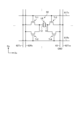
- FIG. 1 is a plan view showing a schematic configuration of a detection device provided with an ultrasonic element according to Embodiment 1.
- FIG. FIG. 2 is a block diagram showing a configuration example of the detection device according to the first embodiment.
- FIG. 3 is a schematic diagram showing a schematic cross-sectional configuration of the detection device of Embodiment 1.
- FIG. 4 is a schematic diagram showing the relationship between the object to be detected and the detection device in the space above the detection area.
- FIG. 5 is a circuit diagram showing one detection area among a plurality of detection areas according to the first embodiment.
- FIG. 6 is a plan view showing the detection area of Embodiment 1.
- FIG. 7 is a timing chart showing the operation of one ultrasonic transducer in Embodiment 1.
- FIG. 8 is a cross-sectional view showing the detection area and the frame area of Embodiment 1.
- FIG. 9 is a cross-sectional view showing the detection area of Embodiment 2.
- FIG. 10 is a cross-sectional view showing the detection area of Embodiment 3.
- FIG. 11 is a cross-sectional view showing the detection area of the fourth embodiment.
- FIG. 12 is a cross-sectional view showing the detection area of the fifth embodiment.
- FIG. 13 is a circuit diagram showing one detection area among a plurality of detection areas according to the fifth embodiment.
- FIG. 14 is a cross-sectional view showing the detection area of Embodiment 6.
- FIG. 15 is a plan view showing the first electrode and the second electrode of Embodiment 6.
- FIG. 16 is a plan view showing a first electrode and a second electrode according to Modification 1 of Embodiment 6.
- FIG. 17 is a plan view showing a first electrode and a second electrode according to Modification 2 of Embodiment 6.
- FIG. 18 is a plan view showing a first electrode and a second electrode according to Modification 3 of Embodiment 6.
- FIG. 19 is a plan view showing a first electrode and a second electrode according to Modification 4 of Embodiment 6.
- FIG. FIG. 20 is a plan view showing the detection area of Embodiment 7.
- FIG. 21 is a cross-sectional view showing the detection area of Embodiment 7.
- FIG. 1 is a plan view showing a schematic configuration of a detection device provided with an ultrasonic element according to Embodiment 1.
- the detection device 1 includes an ultrasonic transducer array 10 and a controller 20 .
- the ultrasonic transducer array 10 has a flexible substrate 51 and a plurality of ultrasonic transducer elements SE provided in the detection area AA of the flexible substrate 51 .
- one first electrode 12 is arranged for one ultrasonic transducer SE.
- the flexible substrate 51 has a frame area GA outside the detection area AA.
- a signal line selection circuit 16 and a scanning circuit 17 are arranged in the frame area GA.
- the control unit 20 has a control board 43 , an ultrasonic processing circuit 40 mounted on the control board 43 , a power supply circuit 41 , and an interface circuit 42 .
- a control board 43 is electrically connected to the flexible board 51 via the wiring board 31 .
- the wiring board 31 is, for example, a flexible printed board.
- the control board 43 is, for example, a rigid board.
- the power supply circuit 41 supplies power to the interface circuit 42 and the ultrasonic processing circuit 40 based on power supplied from the outside.
- the power supply circuit 41 supplies necessary power to the signal line selection circuit 16, the scanning circuit 17, the ultrasonic processing circuit 40, and the ultrasonic transducer SE via the wiring board 31 based on the power supplied from the outside.
- the power supply circuit 41 is a circuit that manages power required for the signal line selection circuit 16 , the scanning circuit 17 , the ultrasonic transducer SE, the interface circuit 42 and the ultrasonic processing circuit 40 .
- the interface circuit 42 is, for example, a USB controller IC, and controls communication between the A/D conversion circuit 23 and a host controller (not shown) of the host device on which the detection system is mounted. Power supplied from the outside is supplied to the power supply circuit 41 via the interface circuit 42 .
- the detection area AA of the flexible substrate 51 is an area provided with a plurality of ultrasonic conversion elements SE arranged in a matrix in the Dx direction (first direction) and the Dy direction (second direction).
- the flexible substrate 51 is, for example, a flexible printed circuit board (FPC Flexible Printed Circuits).
- the Dx direction (first direction) and the Dy direction (second direction) intersect and are orthogonal. Also, in the present disclosure, the direction perpendicular to the Dx direction (first direction) and the Dy direction (second direction) is defined as the Dz direction (third direction).
- ultrasonic transducer elements SE are arranged in the Dx direction and four ultrasonic transducer elements SE are arranged in the Dy direction. It is provided in the detection area AA of the substrate 51 .
- the plurality of ultrasonic transducer elements SE is an ultrasonic transducer array. Note that the plurality of ultrasonic transducer elements SE may be arranged in a staggered arrangement. Also, the number of ultrasonic transducers SE provided in the detection area AA of the flexible substrate 51 is not limited to the embodiment.
- FIG. 2 is a block diagram showing a configuration example of the detection device of Embodiment 1.
- the ultrasonic processing circuit 40 includes a signal transmission circuit 21, a signal detection circuit 22, an A/D conversion circuit 23, a signal processing circuit 24, a coordinate extraction circuit 25, a storage circuit 26, Prepare.
- the ultrasonic processing circuit 40 is, for example, a PLD (Programmable Logic Device) such as an FPGA (Field Programmable Gate Array).
- the signal transmission circuit 21 transmits the oscillation pulse Set(n) (n is a natural number from 1 to N, N is the number of electrodes in the detection area AA) to the ultrasonic transducer. It is delivered to the first electrode 12 (see FIG. 1) of the SE.
- the signal detection circuit 22 is, for example, an analog front end (AFE) IC.
- the signal detection circuit 22 detects the detection signal Det(n) output from the ultrasonic transducer array 10 (n is a natural number from 1 to N, N is a number assigned to the electrodes within the detection area AA, and the maximum The value is the number of electrodes.), the detection value S(n) of each first electrode 12 is generated.
- the A/D conversion circuit 23 samples the detected value S(n) of each first electrode 12 and converts it into a digital signal.
- the signal processing circuit 24 performs predetermined signal processing on the detected value S(n) from the A/D conversion circuit 23 . Specifically, the signal processing circuit 24 performs comparison arithmetic processing of the detected value S(n).
- the coordinate extraction circuit 25 extracts the spatial coordinates of the position where the object to be detected exists based on the result of the comparison operation processing of the signal processing circuit 24 .
- the coordinate extraction circuit 25 uses the detection value S(n) of each first electrode 12 processed by the signal processing circuit 24 to extract a space indicating the position of the object F in the space on the detection area AA shown in FIG. Extract the coordinates R (Rx, Ry, Rz).
- Information on the spatial coordinates R (Rx, Ry, Rz) is output to an external device via the interface circuit 42 (see FIG. 1).
- the storage circuit 26 has a function of storing information on the spatial coordinates R (Rx, Ry, Rz) extracted by the coordinate extraction circuit 25 .
- FIG. 3 is a schematic diagram showing a schematic cross-sectional configuration of the detection device of Embodiment 1.
- the detection device 1 of Embodiment 1 is arranged to face the display panel 200 .
- the detection area AA (see FIG. 1) of the ultrasonic transducer array 10 and the display area DA of the display panel 200 are arranged so as to overlap in the Dz direction (third direction).
- the detection area AA of the ultrasonic transducer array 10 and the display area DA of the display panel 200 are arranged so as to entirely overlap. may be arranged so as to overlap with the
- the display panel 200 is exemplified by, for example, a liquid crystal display (LCD).
- the display panel 200 may be, for example, an organic EL display (OLED: Organic Light Emitting Diode) or an inorganic EL display (micro LED, mini LED).
- OLED Organic Light Emitting Diode
- micro LED mini LED
- the ultrasonic transducer array 10 includes a flexible substrate 51 , a frame layer 52 , a circuit layer 53 , a piezoelectric layer 54 and a protective layer 55 .
- the ultrasonic transducer array 10 is laminated in the order of a frame layer 52 , a flexible substrate 51 , a circuit layer 53 , a piezoelectric layer 54 and a protective layer 55 from the opposite side of the display panel 200 .
- FIG. 4 is a schematic diagram showing the relationship between the object to be detected and the detection device in the space above the detection area.
- the ultrasonic transducer SE converts the oscillation pulse Set(n) to generate an ultrasonic wave Tu, and the ultrasonic wave Tu is transmitted.
- the ultrasonic conversion element SE receives the ultrasonic wave Ru reflected by the object to be detected F (for example, operator's fingers, etc.) and converts it into a detection signal Det(n).
- the coordinate extraction circuit 25 determines whether the detected object F (for example, the operator's fingers, etc.) exists on the detection area AA. Generates spatial coordinates that indicate a position.
- the ultrasonic transducer SE detects the object to be detected F (for example, fingers of the operator) based on the time until it receives the ultrasonic wave Ru reflected by the object to be detected F (for example, fingers of the operator). can also measure the distance of the object to be detected F (for example, fingers of the operator).
- FIG. 5 is a circuit diagram showing one detection area among the plurality of detection areas of the first embodiment.
- FIG. 6 is a plan view showing the detection area of Embodiment 1.
- FIG. 5 is a circuit diagram showing one detection area among the plurality of detection areas of the first embodiment.
- FIG. 6 is a plan view showing the detection area of Embodiment 1.
- the scanning circuit 17 shown in FIG. 1 is a circuit that drives a plurality of scanning lines 61Tx and scanning lines 61Rx shown in FIGS. 5 and 6 based on various control signals.
- the scanning circuit 17 serves both as a driving circuit for scanning the scanning lines 61Tx of the plurality of ultrasonic transducers SE and as a driving circuit for scanning the scanning lines 61Rx of the plurality of ultrasonic transducers SE.
- the scanning circuit 17 sequentially selects a plurality of scanning lines 61Tx and 61Rx, and supplies gate drive signals to the selected scanning lines 61Tx and 61Rx. Thereby, the scanning circuit 17 selects a plurality of ultrasonic transducers SE connected to the scanning lines 61Tx and 61Rx.
- the scanning lines 61Tx and the scanning lines 61Rx are made of metal materials such as aluminum (Al), gold, molybdenum, and titanium.
- the signal line selection circuit 16 is a switch circuit that sequentially or simultaneously selects a plurality of transmission signal lines 62Tx and a plurality of reception signal lines 62Rx.
- the signal line selection circuit 16 is, for example, a multiplexer.
- the signal line selection circuit 16 connects the selected transmission signal line 62Tx and the signal transmission circuit 21 based on the selection signal supplied from the ultrasonic processing circuit 40 .
- the signal line selection circuit 16 connects the selected reception signal line 62Rx and the signal detection circuit 22 based on the selection signal supplied from the ultrasonic processing circuit 40 . Thereby, the signal line selection circuit 16 outputs the detection signal Det(n) of the ultrasonic transducer SE to the signal detection circuit 22 .
- Metal materials such as aluminum (Al), gold, molybdenum, and titanium are used for the transmission signal line 62Tx and the reception signal line 62Rx.
- Each ultrasonic transducer SE includes a first switching element Tr1, a second switching element Tr2, and a membrane vibrator UE.
- the first switching element Tr1 switches and controls the connection between the transmission signal line 62Tx and the membrane vibrator UE.
- the second switching element Tr2 switches and controls the connection between the reception signal line 62Rx and the membrane vibrator UE.
- the first electrode 12 on one end side of the membrane vibrating body UE is connected to the drain of the first switching element Tr1 and the drain of the second switching element Tr2, and the second electrode 14 on the other end side of the membrane vibrating body UE is connected to the reference potential. It is connected to a reference potential wiring 63 to which GND is supplied. As shown in FIG. 6, the first electrode 12 is connected to the drain of the first switching element Tr1 and the drain of the second switching element Tr2 via the connection wiring 12W.
- the transmission signal line 62Tx is connected to the source of the first switching element Tr1.
- the reception signal line 62Rx is connected to the source of the second switching element Tr2.
- the scanning line 61Tx is connected to the gate of the first switching element Tr1.
- the scanning line 61Rx is connected to the gate of the second switching element Tr2.
- the connection to the drain of the first switching element Tr1 and the second switching element Tr2 and the connection to the source of the first switching element Tr1 and the second switching element Tr2 may be interchanged.
- the reference potential wiring 63 is made of a metal material such as aluminum (Al), gold, molybdenum, titanium, or the like.
- the circuits shown in FIGS. 5 and 6 may further include other transistors, signal amplifier circuits, bandpass filters, capacitors, and the like.
- FIG. 7 is a timing chart showing the operation of one ultrasonic transducer in the first embodiment.
- transmission of ultrasonic waves and reception of ultrasonic waves are processed in a time division manner.
- a gate drive signal is transmitted to the scanning line 61Tx selected by the scanning circuit 17, and the signal line selection circuit 16 transmits the oscillation pulse Set(n) from the signal transmission circuit 21 to the selected transmission signal line 62Tx. transmit.
- the membrane vibrator UE vibrates based on the oscillation pulse Set(n) to generate the ultrasonic waves Tu.
- the frequency of the ultrasonic wave Tu is, for example, 1 kHz or more and 1 MHz or less.
- a gate drive signal is transmitted to the scanning line 61Rx selected by the scanning circuit 17, and the signal line selection circuit 16 connects the selected reception signal line 62Rx and the signal detection circuit 22.
- the membrane vibrator UE Upon receiving the ultrasonic wave Ru, the membrane vibrator UE converts the ultrasonic wave Ru into a detection signal Det(n) of an electric signal, and the detection signal Det(n) is transmitted to the signal detection circuit 22 .
- the timing at which the gate driving signal is transmitted to the scanning line 61Tx and the timing at which the gate driving signal is transmitted to the scanning line 61Rx are shifted.
- the timings at which the drive signals are transmitted may be the same. By doing so at the same time, although there is a risk of crosstalk between the oscillation pulse Set(n) and the detection signal Det(n), a closer object can be detected.
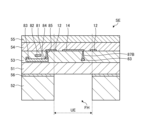
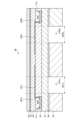
- FIG. 8 is a cross-sectional view showing the detection area and the frame area of Embodiment 1.
- the flexible substrate 51 on which the cross section of one ultrasonic transducer SE in the detection area AA is described together with the cross section of the frame area GA is a flexible resin substrate, such as polyimide resin. Used.
- the thickness of the flexible substrate 51 is 1 ⁇ m or more and 100 ⁇ m or less.
- a cavity FH is opened in the frame layer 52 for each ultrasonic transducer SE.
- a region that overlaps with the cavity FH in plan view becomes the membrane vibrator UE.
- the cavity FH surrounds the first electrode 12 in plan view.
- the frame layer 52 is, for example, polyimide resin or metal foil.
- the thickness of the frame layer 52 is 1 ⁇ m or more and 100 ⁇ m or less.
- the frame layer 52 is less bendable than the flexible substrate 51 .
- the frame layer 52 is made of the same material as the flexible substrate 51, so that the frame layer 52 is thicker than the flexible substrate 51, so that the flexible substrate overlaps the first electrode 12 and the cavity FH in plan view. 51 vibrate together and function as a membrane vibrator UE.
- the Young's modulus and thickness of the frame layer 52 are set so that the frame layer 52 is more difficult to bend than the flexible substrate 51 .
- the cavity FH is circular with a diameter ⁇ D.
- Diameter ⁇ D is smaller than the range surrounded by scanning lines 61Tx, scanning lines 61Rx, transmission signal lines 62Tx, and reception signal lines 62Rx shown in FIG.
- the diameter ⁇ D is, for example, 0.1 mm or more and 5 mm or less.
- the piezoelectric layer 54 is made of an inorganic material such as PZT (lead zirconate titanate) or AlN (aluminum nitride), or an organic material such as polyvinylidene fluoride resin (polyvinylidene difluoride resin).
- the thickness of the piezoelectric layer 54 is, for example, 10 nm or more and 10000 nm or less.
- the piezoelectric layer 54 may optionally include buffer layers, crystal adjustment layers, protective layers, matching layers, backing layers, and the like.
- the piezoelectric layer 54 is formed over the entire sensing area AA.
- the area where the piezoelectric layer 54 is formed may have the same size as the area of the cavity FH in plan view, and may be provided so as to overlap the area of the cavity FH in plan view.
- the piezoelectric layer 54 may have a similar shape to the area of the cavity FH in plan view, and may be larger than the boundary of the area of the cavity FH.
- the piezoelectric layer 54 may be similar in shape to the area of the cavity FH in plan view, smaller than the area of the cavity FH, and larger than the first electrode 12 .
- the circuit layer 53 and piezoelectric layer 54 are formed on a glass substrate, and the circuit layer 53 and piezoelectric layer 54 are transferred from the glass substrate to the flexible substrate 51 .
- a piezoelectric layer 54 is formed on the glass substrate.
- a first electrode 12 is formed on the piezoelectric layer 54 .
- a first resin layer 71 is formed on the first electrode 12 .
- Metal materials such as aluminum (Al), gold, molybdenum, and titanium are used for the first electrode 12 .
- the first electrode 12 may be an alloy material containing at least one of these metal materials or a laminate of at least two of these metal materials.
- a gate electrode 82 is formed on the first resin layer 71 when viewed from the glass substrate.
- a second resin layer 72 is laminated on the gate electrode 82 .
- a source electrode 83 and a drain electrode 84 are formed on the second resin layer 72 .
- the drain electrode 84 and the first electrode 12 are electrically connected via a through hole 85 .
- the second resin layer 72 around the source electrode 83 and the drain electrode 84 is covered with a third resin layer 73 .
- a semiconductor layer 81 is formed on the source electrode 83 and the drain electrode 84, and the semiconductor layer 81 and the source electrode 83 and the drain electrode 84 are bonded to each other.
- the semiconductor layer 81, gate electrode 82, source electrode 83 and drain electrode 84 function as a first switching element Tr1.
- the gate electrode 82, the source electrode 83, the drain electrode 84, and the through hole 8 are made of metal material such as aluminum (Al), gold, molybdenum, and titanium.
- the gate electrode 82, the source electrode 83, the drain electrode 84, and the through hole 85 may be an alloy material containing at least one of these metal materials or a laminate of at least two of these metal materials. Since the second switching element Tr2 has the same configuration as the first switching element Tr1, detailed description thereof will be omitted.
- the semiconductor layer 81 is an oxide semiconductor. More preferably, the semiconductor layer 81 is a transparent amorphous oxide semiconductor (TAOS) among oxide semiconductors. Leakage current is suppressed by using an oxide semiconductor for the semiconductor layer 81 . That is, it is possible to reduce the leak current from the non-selected transistor of the first switching element Tr1 or the second switching element Tr2. Therefore, the detection device 1 can improve the S/N ratio.
- the semiconductor layer 81 is not limited to this, and may be a microcrystalline oxide semiconductor, an amorphous oxide semiconductor, polysilicon, low temperature polysilicon (LTPS: Low Temperature Polycrystalline Silicon), or the like.
- a fourth resin layer 74 is formed on the semiconductor layer 81 and the third resin layer 73 . Since the circuit layer 53 is transferred from the glass substrate to the flexible substrate 51, the stacking order is reversed when viewed from the flexible substrate 51. FIG.
- the second resin layer 72 is an inorganic insulating film such as silicon nitride.
- the first resin layer 71, the third resin layer 73, and the fourth resin layer 74 may be inorganic insulating films or organic insulating films, and are organic insulating films such as acrylic resin, for example. If the first resin layer 71, the third resin layer 73, and the fourth resin layer 74 are organic insulating films, the circuit layer 53 is less likely to crack. The thickness of the circuit layer 53 may be partially changed. It may be thinned or removed.
- a second electrode 14 is formed on the second surface opposite to the first surface of the piezoelectric layer 54 on which the first electrode 12 is formed.
- the second electrode 14 is also called a counter electrode, and is connected via a through hole 87 to the reference potential wiring 63 in the frame area GA.
- Metal materials such as aluminum (Al), gold, molybdenum, and titanium are used for the second electrode 14 .
- the second electrode 14 may be an alloy material containing at least one of these metal materials or a laminate of at least two of these metal materials.
- the second electrode 14 is covered with a protective layer 55 of an organic insulating film such as acrylic resin.
- the second electrode 14 is in contact with the surface of the piezoelectric layer 54 opposite to the surface with which the first electrode 12 is in contact, and the piezoelectric layer 54 is sandwiched between the first electrode 12 and the second electrode 14 .
- the second electrode 14 is provided across the plurality of ultrasonic transducers SE, and serves as the second electrode 14 common to the plurality of ultrasonic transducers SE. This reduces the electrical resistance of the second electrode 14 .
- the flexible substrate 51 and the frame layer 52 are bonded via an adhesive layer 56 .
- the adhesive layer 56 has tackiness on both sides, and has a cavity FH formed by press working or the like while being bonded to the frame layer 52 .
- the ultrasonic transducer SE is formed by transfer in the example shown in FIG. 8, it may be formed by other methods.
- a flexible substrate 51 is formed on a glass substrate, and a circuit layer 53, a piezoelectric layer 54, a second electrode 14, and a protective layer 55 are formed thereon. After that, the flexible substrate 51 may be separated from the glass substrate, and the flexible substrate 51 and the frame layer 52 may be bonded.
- the circuit layer 53, the piezoelectric layer 54, the second electrode 14, and the protective layer 55 are sequentially laminated, the order of lamination is not reversed even when viewed from the flexible substrate 51.
- the first switching element Tr1 is provided at a position that does not overlap the cavity FH in plan view, and the first switching element Tr1 and the first electrode 12 are electrically connected at a position that does not overlap the cavity FH in plan view. .
- the frame layer 52 may be formed by covering the region of the cavity FH with a photoresist, coating or forming a film around the photoresist, and then removing the photoresist.
- the frame layer 52 may be 3D printed and directly formed on the surface of the flexible substrate 51 .
- the detection device 1 of Embodiment 1 includes a plurality of ultrasonic transducers SE that transmit and receive ultrasonic waves.
- the detection device 1 includes a laminate and a frame layer 52 laminated to a first surface of the laminate and a second surface opposite to the first surface.
- the laminate includes a flexible substrate 51 , a circuit layer 53 laminated on the flexible substrate 51 , and a piezoelectric layer 54 laminated on the circuit layer 53 .
- the frame layer 52 is bonded to the flexible substrate 51 .
- the ultrasonic transducer SE includes a first electrode 12 in contact with the piezoelectric layer 54 and a second electrode 14 in contact with the piezoelectric layer 54 .
- the frame layer 52 has a cavity FH at a position overlapping the first electrode 12 in plan view.
- the flexible substrate 51 bends more easily in response to vibration than a substrate made of glass, silicon, or the like, so that the bonding surfaces of the flexible substrate 51, the circuit layer 53, and the piezoelectric layer 54 are less likely to break. Further, the membrane vibrator UE can be manufactured at low cost only by bonding the flexible substrate 51 and the frame layer 52 having the cavity FH.
- FIG. 9 is a cross-sectional view showing the detection area of Embodiment 2.
- FIG. 9 the same reference numerals are assigned to the same configurations as in the first embodiment, and the description may be omitted.
- a cross-section of one ultrasonic transducer SE of the detection area AA is shown.
- the frame layer 52 is bonded to one surface of the flexible substrate 51, but in the second embodiment, the frame layer 52 is attached to the circuit layer 53 and the piezoelectric layer 54 on the opposite side of the first embodiment. It is in.
- the frame layer 52 is bonded to one surface of the protective layer 55 via an adhesive layer 56 .
- a cavity FH is opened in the frame layer 52 for each ultrasonic transducer SE.
- the detection device 1 of Embodiment 2 includes a plurality of ultrasonic transducers SE that transmit and receive ultrasonic waves.
- the detection device 1 includes a laminate and a frame layer 52 laminated to the second of the first side of the laminate and the second side opposite to the first side.
- the laminate includes a flexible substrate 51 , a circuit layer 53 laminated on the flexible substrate 51 , and a piezoelectric layer 54 laminated on the circuit layer 53 .
- the frame layer 52 is bonded to a protective layer 55 on the opposite side of the laminate from the flexible substrate 51 .
- the ultrasonic transducer SE includes a first electrode 12 in contact with the piezoelectric layer 54 and a second electrode 14 in contact with the piezoelectric layer 54 .
- the frame layer 52 has a cavity FH at a position overlapping the first electrode 12 in plan view.
- the flexible substrate 51 bends more easily in response to vibration than a substrate made of glass, silicon, or the like, so that the bonding surfaces of the flexible substrate 51, the circuit layer 53, and the piezoelectric layer 54 are less likely to break. Further, the membrane vibrator UE can be manufactured at low cost only by bonding the flexible substrate 51 and the frame layer 52 having the cavity FH.
- FIG. 10 is a cross-sectional view showing the detection area of Embodiment 3.
- FIG. 10 shows a cross section of one ultrasonic transducer SE of the detection area AA.
- a frame layer 52A is bonded to one surface of the flexible substrate 51 via an adhesive layer 56A.
- a cavity FHA is opened in the frame layer 52A for each ultrasonic transducer SE.
- a frame layer 52B is bonded to one surface of the protective layer 55 via an adhesive layer 56B.
- a cavity FHB is opened in the frame layer 52B for each ultrasonic transducer SE.
- the detection device 1 of Embodiment 3 includes a plurality of ultrasonic transducers SE that transmit and receive ultrasonic waves.
- the detection device 1 includes a laminate, a frame layer 52A laminated on a first side of the laminate, and a frame layer 52B laminated on a second side opposite to the first side.
- the laminate includes a flexible substrate 51 , a circuit layer 53 laminated on the flexible substrate 51 , and a piezoelectric layer 54 laminated on the circuit layer 53 .
- the circuit layer 53 and the piezoelectric layer 54 are sandwiched between the frame layers 52A and 52B.
- the ultrasonic transducer SE includes a first electrode 12 in contact with the piezoelectric layer 54 and a second electrode 14 in contact with the piezoelectric layer 54 .
- the frame layer 52 has a cavity FHA and a cavity FHB at positions overlapping the first electrode 12 in plan view.
- the cavity FHA of one frame layer 52A and the cavity FHB of the other frame layer 52B are positioned to overlap each other in plan view.
- the flexible substrate 51 bends more easily in response to vibration than a substrate made of glass, silicon, or the like, so that the bonding surfaces of the flexible substrate 51, the circuit layer 53, and the piezoelectric layer 54 are less likely to break. Further, the membrane vibrator UE can be manufactured at low cost only by bonding the flexible substrate 51 and the frame layer 52 having the cavity FH.
- FIG. 11 is a cross-sectional view showing the detection area of the fourth embodiment.
- the same reference numerals are assigned to the same configurations as in the first to third embodiments, and the description thereof may be omitted.
- FIG. 11 shows a cross-section of one ultrasonic transducer SE of the detection area AA.
- a reference potential wiring 63 is routed to each ultrasonic transducer SE.
- the reference potential wiring 63 is formed in a layer different from that of the source electrode 83 and the drain electrode 84, and is formed in the same layer as the semiconductor layer 81, for example.
- a relay wiring 88 in the same layer as the first electrode 12 is connected to the reference potential wiring 63 via a through hole 87A.
- the second electrode 14 and the relay wiring 88 are connected via a through hole 89 . Thereby, the frame area GA can be narrowed.
- the second electrode 14 of each ultrasonic transducer SE is provided in a region overlapping the cavity FH in plan view. Since adjacent second electrodes 14 are separated from each other, crosstalk of ultrasonic waves Ru detected by adjacent ultrasonic transducer elements SE is reduced.
- the second electrode 14 and the reference potential wiring 63 are electrically connected at a position not overlapping the cavity FH in plan view, the possibility of disconnection of the reference potential wiring 63 is reduced.
- FIG. 12 is a cross-sectional view showing the detection area of the fifth embodiment.
- FIG. 13 is a circuit diagram showing one detection area among a plurality of detection areas according to the fifth embodiment.
- the same reference numerals are assigned to the same configurations as in the first to fourth embodiments, and the description thereof may be omitted.
- FIG. 12 shows a cross-section of one ultrasonic transducer SE of the detection area AA.
- the second electrode 14 is electrically connected to the third switching element Tr3. Since the third switching element Tr3 has the same configuration as the first switching element Tr1, detailed description thereof will be omitted.
- the drain electrode 84 of the third switching element Tr3 and the second electrode 14 are electrically connected via a through hole 85, a relay wiring 88 and a through hole 89. As shown in FIG.
- Each ultrasonic transducer SE includes a first switching element Tr1, a second switching element Tr2, a third switching element Tr3, a fourth switching element Tr4, and a membrane vibrator UE.
- the first switching element Tr1 switches and controls the connection between the transmission signal line 62Tx and the membrane vibrator UE.
- the second switching element Tr2 switches and controls the connection between the reception signal line 62Rx and the membrane vibrator UE.
- the third switching element Tr3 switches and controls the connection between the transmission signal line 62Txx and the membrane vibrator UE.
- the second switching element Tr2 switches and controls the connection between the reference potential wiring 63 and the membrane vibrator UE.
- the second electrode 14 is connected to the drain of the third switching element Tr3.
- the transmission signal line 62Txx is connected to the source of the third switching element Tr3.
- a signal opposite in phase to the oscillation pulse Set(n) of the transmission signal line 62Tx (first transmission signal line) is transmitted to the transmission signal line 62Txx (second transmission signal line).
- the second electrode 14 is connected to the drain of the fourth switching element Tr4.
- the reference potential wiring 63 is connected to the source of the fourth switching element Tr4.
- the first switching element Tr1 and the third switching element Tr3 are simultaneously turned on, and the second switching element Tr2 and the fourth switching element Tr4 are simultaneously turned off.
- the transmission signal line 62Tx transmits the signal of the oscillation pulse Set(n) to the first electrode 12 via the first switching element Tr1
- the transmission signal line 62Txx transmits the signal to the second electrode 14 via the third switching element Tr3.
- a signal opposite in phase to the oscillation pulse Set(n) is transmitted.
- the amplitude of the signal applied to the piezoelectric layer 54 is double that of the first embodiment, and the ultrasonic output is improved.
- the first switching element Tr1 and the third switching element Tr3 are simultaneously turned off, and the second switching element Tr2 and the fourth switching element Tr4 are simultaneously turned on.
- the reception signal line 62Rx and the first electrode 12 are connected via the second switching element Tr2, and the reference potential wiring 63 and the second electrode 14 are connected via the third switching element Tr3.
- the detection signal Det(n) of the ultrasonic transducer SE is output to the signal detection circuit 22 .
- the second electrode 14 of each ultrasonic transducer SE is provided in a region overlapping the cavity FH in plan view. Adjacent second electrodes 14 are separated from each other. In the ultrasonic transducers SE not selected by the scanning circuit 17, the second electrode 14 becomes the reference potential GND, and noise from the ultrasonic transducers SE not selected by the scanning circuit 17 is suppressed.
- the reverse running signal of the oscillation pulse Set(n) is transmitted to the second electrode 14, so the amplitude of the membrane vibrator UE increases.
- the second electrode 14 becomes the reference potential GND, and the influence of the vibration of the other ultrasonic transducers SE can be suppressed.
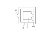
- FIG. 14 is a cross-sectional view showing the detection area of Embodiment 6.
- FIG. 15 is a plan view showing the first electrode and the second electrode of Embodiment 6.
- FIG. 14 is the XIV-XIV cross section of FIG.
- the same components as in Embodiments 1 to 5 are denoted by the same reference numerals, and description thereof may be omitted.
- FIG. 14 shows a cross-section of one ultrasonic transducer SE of the detection area AA.
- a reference potential wiring 63 is routed to each ultrasonic transducer SE.
- the reference potential wiring 63 is formed in a layer different from that of the source electrode 83 and the drain electrode 84, and is formed in the same layer as the semiconductor layer 81, for example.
- the second electrode 14 in the same layer as the first electrode 12 is connected to the reference potential wiring 63 via the through hole 87B. As shown in FIG. 15, the second electrode 14 is in contact with the same side of the piezoelectric layer 54 as the first electrode 12 is in contact with. And the second electrode 14 is inside the second electrode 14 . Thereby, the frame area GA can be narrowed.
- the second electrode 14 of each ultrasonic transducer SE is provided in a region overlapping the cavity FH in plan view. Since adjacent second electrodes 14 are separated from each other, crosstalk of ultrasonic waves Ru detected by adjacent ultrasonic transducer elements SE is reduced.
- the area where the second electrode 14 is formed has a similar shape to the area of the cavity FH in plan view and is smaller than the area of the cavity FH.
- the area where the first electrode 12 is formed overlaps with the boundary of the area of the cavity FH in plan view, and the first electrode 12 has an annular shape.
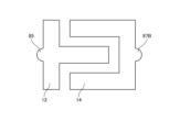
- FIG. 16 is a plan view showing the first electrode and the second electrode according to Modification 1 of Embodiment 6.
- FIG. 16 in Modification 1, the second electrode 14 is rectangular, and the outer diameter of the first electrode 12 is rectangular and annular.
- the first electrode 12 and the second electrode 14 are the same layer as in the sixth embodiment.
- FIG. 17 is a plan view showing a first electrode and a second electrode according to Modification 2 of Embodiment 6.
- FIG. 17 the region where the second electrode 14 is formed is similar in shape to the region of the cavity FH in plan view, and is smaller than the region of the cavity FH.
- the area where the first electrode 12 is formed overlaps with the boundary of the area of the cavity FH in plan view, and the first electrode 12 has an annular shape. Note that the first electrode 12 and the second electrode 14 are the same layer as in the sixth embodiment.
- a through hole 87B is arranged outside the first electrode 12, and the through hole 87B and the second electrode 14 are connected by wiring.
- the reference potential wiring 63 does not overlap with the region overlapping the cavity FH region in plan view, so that the reference potential wiring 63 is less susceptible to the vibration of the membrane vibrating body UE, and the reliability of the detection device 1 is improved. improves.
- FIG. 18 is a plan view showing a first electrode and a second electrode according to Modification 3 of Embodiment 6.
- FIG. 18 As shown in FIG. 18, in Modification 3, the first electrode 12 and the second electrode 14 are rectangular, and the first electrode 12 and the second electrode 14 are adjacent to each other. Note that the first electrode 12 and the second electrode 14 are the same layer as in the sixth embodiment.
- a through-hole 87B is arranged at a position outside an area overlapping with the area of the cavity FH in plan view, and the through-hole 87B and the second electrode 14 are connected by wiring.
- the reference potential wiring 63 does not overlap with the region overlapping the cavity FH region in plan view, so that the reference potential wiring 63 is less susceptible to the vibration of the membrane vibrating body UE, and the reliability of the detection device 1 is improved. improves.
- FIG. 19 is a plan view showing a first electrode and a second electrode according to Modification 4 of Embodiment 6.
- FIG. 19 As shown in FIG. 19, in Modification 4, the first electrode 12 and the second electrode 14 are interdigitated comb electrodes. Note that the first electrode 12 and the second electrode 14 are the same layer as in the sixth embodiment.
- a through-hole 87B is arranged at a position outside an area overlapping with the area of the cavity FH in plan view, and the through-hole 87B and the second electrode 14 are connected by wiring.
- the reference potential wiring 63 does not overlap with the region overlapping the cavity FH region in plan view, so that the reference potential wiring 63 is less susceptible to the vibration of the membrane vibrating body UE, and the reliability of the detection device 1 is improved. improves.
- FIG. 20 is a plan view showing the detection area of Embodiment 7.
- FIG. 21 is a cross-sectional view showing the detection area of Embodiment 7.
- FIG. 20 is the XX-XX' section of FIG.
- the same components as in Embodiments 1 to 6 are denoted by the same reference numerals, and description thereof may be omitted.
- a cross section of one ultrasonic transducer SE of the detection area AA is shown.
- the first electrode 12Tx and the first electrode 12Rx are arranged for one ultrasonic transducer SE.
- the first electrode 12Tx is an ultrasonic transmitting electrode that generates an ultrasonic wave Tu
- the first electrode 12Rx is an ultrasonic receiving electrode that receives an ultrasonic wave Ru.
- Each ultrasonic transducer SE includes a first switching element Tr1, a second switching element Tr2, a membrane oscillator UETx, and a membrane oscillator UERx.
- the first switching element Tr1 and the first electrode 12Tx are electrically connected via a through hole 85Tx.
- the first switching element Tr1 switches and controls the connection between the transmission signal line 62Tx and the membrane vibrator UETx.
- the second switching element Tr2 and the first electrode 12Rx are electrically connected via a through hole 85Rx.
- the second switching element Tr2 switches and controls the connection between the reception signal line 62Rx and the membrane vibrator UERx.
- a first cavity FHTx and a second cavity FHRx are opened in the frame layer 52 for each ultrasonic transducer SE.
- the frame layer 52 has a first cavity FHTx at a position overlapping with one of the first electrodes 12Tx in plan view, and a second cavity FHRx at a position overlapping with the other first electrode 12Rx.
- a region that overlaps with the first cavity FHTx in plan view becomes the membrane vibrator UETx.
- a region that overlaps with the second cavity FHRx in plan view becomes the membrane vibrator UERx.
- Ultrasonic wave transmission and ultrasonic wave reception are processed in a time-division manner.
- the membrane vibrating body UETx and the membrane vibrating body UERx are operated separately.
- the vibrator UERx is less affected.
- the detection device 1 has a shorter detection cycle and improved detection accuracy.
- the first electrode 12Tx may be arranged on the first row of ultrasonic transducer elements SE, and the first electrode 12Rx may be arranged on the second row of ultrasonic transducer elements SE.
Landscapes
- Engineering & Computer Science (AREA)
- Physics & Mathematics (AREA)
- General Engineering & Computer Science (AREA)
- Theoretical Computer Science (AREA)
- Acoustics & Sound (AREA)
- Human Computer Interaction (AREA)
- General Physics & Mathematics (AREA)
- Signal Processing (AREA)
- Transducers For Ultrasonic Waves (AREA)
Abstract
Provided is a detection device having a highly reliable ultrasonic conversion element with low cost. The detection device comprises a laminated body and a frame layer that is laminated on at least one of a first surface and second surface of the laminated body, the second surface being positioned on the opposite side of the first surface. The laminated body comprises a flexible substrate, a circuit layer including a plurality of first electrodes and laminated on the flexible substrate, and a piezoelectric layer laminated on the circuit layer. One ultrasonic conversion element comprises at least one first electrode contacting the piezoelectric layer and at least one second electrode contacting the piezoelectric layer. The frame layer has a cavity at a position overlapping with the first electrode in a plan view.
Description
本開示は、超音波を利用した超音波変換素子及びそれを用いた検出装置に関する。
The present disclosure relates to an ultrasonic transducer using ultrasonic waves and a detection device using the same.
超音波変換素子が知られている(例えば、特許文献1、2参照)。
An ultrasonic transducer is known (see Patent Documents 1 and 2, for example).
超音波変換素子は、圧電層に接するキャビティをアンカー構造体やガラスやシリコンなどの基板に形成する必要がある。アンカー構造体にキャビティを設けると、圧電層とアンカー構造体とが接合する、貼り合わせ面が振動するので、強度が不足する可能性がある。また、基板の裏面を裏面エッチングしてキャビティを製造するには、コストがかかる可能性がある。
For ultrasonic transducers, it is necessary to form a cavity in contact with the piezoelectric layer in the anchor structure or substrate such as glass or silicon. If a cavity is provided in the anchor structure, the bonding surface where the piezoelectric layer and the anchor structure are bonded vibrates, which may result in insufficient strength. Also, manufacturing cavities by back etching the back side of the substrate can be costly.
本開示は、低コストで、信頼性の高い超音波変換素子を有する検出装置を提供することを目的とする。
An object of the present disclosure is to provide a detection device having a low-cost, highly reliable ultrasonic transducer.
本開示の一態様の検出装置は、超音波を送受信する複数の超音波変換素子を含む検出装置であって、可撓性基板と、複数の第1電極及び少なくとも1つの第2電極を含み、かつ前記可撓性基板に積層された回路層と、前記回路層に積層された圧電層と、を含む積層体と、前記積層体の第1面及び前記第1面の反対側の第2面の少なくとも1つの面に積層するフレーム層と、を含み、1つの前記超音波変換素子は、前記圧電層に接する少なくとも1つの前記第1電極と、前記圧電層に接する少なくとも1つの前記第2電極と、を含み、前記フレーム層には、平面視して前記第1電極と重なる位置に、キャビティがある。
A detection device according to one aspect of the present disclosure is a detection device including a plurality of ultrasonic transducers that transmit and receive ultrasonic waves, the detection device including a flexible substrate, a plurality of first electrodes and at least one second electrode, a laminate including a circuit layer laminated on the flexible substrate and a piezoelectric layer laminated on the circuit layer; and a first surface of the laminate and a second surface opposite to the first surface. a frame layer laminated on at least one surface of the ultrasonic transducer, wherein the one ultrasonic transducer includes at least one first electrode in contact with the piezoelectric layer and at least one second electrode in contact with the piezoelectric layer and, the frame layer has a cavity at a position overlapping with the first electrode in plan view.
本開示を実施するための形態(実施形態)につき、図面を参照しつつ詳細に説明する。なお、以下の実施形態に記載した内容により本開示が限定されるものではない。また、以下に記載した構成要素には、当業者が容易に想定できるもの、実質的に同一のものが含まれる。さらに、以下に記載した構成要素は適宜組み合わせることが可能である。また、開示はあくまで一例にすぎず、当業者において、発明の主旨を保っての適宜変更について容易に想到し得るものについては、当然に本開示の範囲に含有されるものである。また、図面は説明をより明確にするため、実際の態様に比べ、各部の幅、厚さ、形状等について模式的に表される場合があるが、あくまで一例であって、本開示の解釈を限定するものではない。また、本明細書と各図において、既出の図に関して前述したものと同様の要素には、同一の符号を付して、詳細な説明を適宜省略することがある。
A form (embodiment) for carrying out the present disclosure will be described in detail with reference to the drawings. The present disclosure is not limited by the contents described in the following embodiments. In addition, the components described below include those that can be easily assumed by those skilled in the art and those that are substantially the same. Furthermore, the components described below can be combined as appropriate. Moreover, the disclosure is merely an example, and those skilled in the art can easily conceive appropriate modifications while maintaining the gist of the invention are, of course, included in the scope of the present disclosure. In addition, in order to make the description clearer, the drawings may schematically show the width, thickness, shape, etc. of each part compared to the actual embodiment, but this is only an example, and the interpretation of the present disclosure is not intended. It is not limited. In addition, in this specification and each figure, the same reference numerals may be given to the same elements as those described above with respect to the existing figures, and detailed description thereof may be omitted as appropriate.
(実施形態1)
図1は、実施形態1の超音波素子を備える検出装置の概略構成を示す平面図である。図1に示すように、検出装置1は、超音波変換アレイ10と、制御部20と、を備える。 (Embodiment 1)
FIG. 1 is a plan view showing a schematic configuration of a detection device provided with an ultrasonic element according toEmbodiment 1. FIG. As shown in FIG. 1 , the detection device 1 includes an ultrasonic transducer array 10 and a controller 20 .
図1は、実施形態1の超音波素子を備える検出装置の概略構成を示す平面図である。図1に示すように、検出装置1は、超音波変換アレイ10と、制御部20と、を備える。 (Embodiment 1)
FIG. 1 is a plan view showing a schematic configuration of a detection device provided with an ultrasonic element according to
超音波変換アレイ10は、可撓性基板51と、可撓性基板51の検出領域AAに設けられる複数の超音波変換素子SEと、を有する。実施形態1では、1つの超音波変換素子SEについて、1つの第1電極12が配置されている。可撓性基板51は、検出領域AAの外側に額縁領域GAを有している。額縁領域GAには、信号線選択回路16と、走査回路17とが配置されている。制御部20は、制御基板43と、制御基板43に実装された、超音波処理回路40と、電源回路41と、インターフェース回路42と、を有する。
The ultrasonic transducer array 10 has a flexible substrate 51 and a plurality of ultrasonic transducer elements SE provided in the detection area AA of the flexible substrate 51 . In Embodiment 1, one first electrode 12 is arranged for one ultrasonic transducer SE. The flexible substrate 51 has a frame area GA outside the detection area AA. A signal line selection circuit 16 and a scanning circuit 17 are arranged in the frame area GA. The control unit 20 has a control board 43 , an ultrasonic processing circuit 40 mounted on the control board 43 , a power supply circuit 41 , and an interface circuit 42 .
可撓性基板51には、配線基板31を介して制御基板43が電気的に接続される。配線基板31は、例えばフレキシブルプリント基板である。制御基板43は、例えばリジット基板である。
A control board 43 is electrically connected to the flexible board 51 via the wiring board 31 . The wiring board 31 is, for example, a flexible printed board. The control board 43 is, for example, a rigid board.
電源回路41は、外部から供給された電力を基に、インターフェース回路42及び超音波処理回路40に電力供給を行う。電源回路41は、外部から供給された電力を基に、配線基板31を介して信号線選択回路16、走査回路17、超音波処理回路40、超音波変換素子SEに必要な電力を供給する。電源回路41は、信号線選択回路16、走査回路17、超音波変換素子SE、インターフェース回路42及び超音波処理回路40に必要な電力の電力管理を行う回路である。
The power supply circuit 41 supplies power to the interface circuit 42 and the ultrasonic processing circuit 40 based on power supplied from the outside. The power supply circuit 41 supplies necessary power to the signal line selection circuit 16, the scanning circuit 17, the ultrasonic processing circuit 40, and the ultrasonic transducer SE via the wiring board 31 based on the power supplied from the outside. The power supply circuit 41 is a circuit that manages power required for the signal line selection circuit 16 , the scanning circuit 17 , the ultrasonic transducer SE, the interface circuit 42 and the ultrasonic processing circuit 40 .
インターフェース回路42は、例えばUSBコントローラICであり、A/D変換回路23と検出システムが搭載されるホストデバイスのホストコントローラ(不図示)との間の通信制御を行う。インターフェース回路42を介して、外部から供給された電力が電源回路41へ供給される。
The interface circuit 42 is, for example, a USB controller IC, and controls communication between the A/D conversion circuit 23 and a host controller (not shown) of the host device on which the detection system is mounted. Power supplied from the outside is supplied to the power supply circuit 41 via the interface circuit 42 .
可撓性基板51の検出領域AAは、Dx方向(第1方向)及びDy方向(第2方向)にマトリクス状に並ぶ複数の超音波変換素子SEが設けられた領域である。可撓性基板51は、例えば、フレキシブルプリント基板(FPCFlexible Printed Circuits)である。
The detection area AA of the flexible substrate 51 is an area provided with a plurality of ultrasonic conversion elements SE arranged in a matrix in the Dx direction (first direction) and the Dy direction (second direction). The flexible substrate 51 is, for example, a flexible printed circuit board (FPC Flexible Printed Circuits).
本開示において、Dx方向(第1方向)及びDy方向(第2方向)は、交差しており、直交している。また、本開示では、Dx方向(第1方向)及びDy方向(第2方向)に直交する方向をDz方向(第3方向)としている。
In the present disclosure, the Dx direction (first direction) and the Dy direction (second direction) intersect and are orthogonal. Also, in the present disclosure, the direction perpendicular to the Dx direction (first direction) and the Dy direction (second direction) is defined as the Dz direction (third direction).
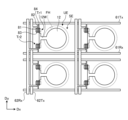
図1に示すように、Dx方向に5つの超音波変換素子SEが並び、Dy方向に4つの超音波変換素子SEが並ぶ、5×4(=20)の超音波変換素子SEが可撓性基板51の検出領域AAに、設けられている。複数の超音波変換素子SEは、超音波変換アレイである。なお、複数の超音波変換素子SEは、千鳥配置で並べられていてもよい。また、可撓性基板51の検出領域AAに設けられる超音波変換素子SEの数は、実施形態に限定されない。
As shown in FIG. 1, five ultrasonic transducer elements SE are arranged in the Dx direction and four ultrasonic transducer elements SE are arranged in the Dy direction. It is provided in the detection area AA of the substrate 51 . The plurality of ultrasonic transducer elements SE is an ultrasonic transducer array. Note that the plurality of ultrasonic transducer elements SE may be arranged in a staggered arrangement. Also, the number of ultrasonic transducers SE provided in the detection area AA of the flexible substrate 51 is not limited to the embodiment.
図2は、実施形態1の検出装置の構成例を示すブロック図である。図2に示すように、超音波処理回路40は、信号送出回路21、信号検出回路22と、A/D変換回路23と、信号処理回路24と、座標抽出回路25と、記憶回路26と、を備える。超音波処理回路40は、例えばFPGA(Field Programmable Gate Array)等のPLD(Programmable Logic Device)である。
FIG. 2 is a block diagram showing a configuration example of the detection device of Embodiment 1. FIG. As shown in FIG. 2, the ultrasonic processing circuit 40 includes a signal transmission circuit 21, a signal detection circuit 22, an A/D conversion circuit 23, a signal processing circuit 24, a coordinate extraction circuit 25, a storage circuit 26, Prepare. The ultrasonic processing circuit 40 is, for example, a PLD (Programmable Logic Device) such as an FPGA (Field Programmable Gate Array).
信号送出回路21は、信号処理回路24からの信号に基づいて、発振パルスSet(n)(nは、1からNまでの自然数、Nは、検出領域AA内の電極数)を超音波変換素子SEの第1電極12(図1参照)へ送出する。
Based on the signal from the signal processing circuit 24, the signal transmission circuit 21 transmits the oscillation pulse Set(n) (n is a natural number from 1 to N, N is the number of electrodes in the detection area AA) to the ultrasonic transducer. It is delivered to the first electrode 12 (see FIG. 1) of the SE.
信号検出回路22は、例えばアナログフロントエンド(AFE:Analog Front End)ICである。信号検出回路22は、超音波変換アレイ10から出力される検出信号Det(n)(nは、1からNまでの自然数、Nは、検出領域AA内の電極に割り当てられた番号であり、最大値は、電極数となる。)に基づき、各第1電極12の検出値S(n)を生成する。A/D変換回路23は、各第1電極12の検出値S(n)をそれぞれサンプリングしてデジタル信号に変換する。
The signal detection circuit 22 is, for example, an analog front end (AFE) IC. The signal detection circuit 22 detects the detection signal Det(n) output from the ultrasonic transducer array 10 (n is a natural number from 1 to N, N is a number assigned to the electrodes within the detection area AA, and the maximum The value is the number of electrodes.), the detection value S(n) of each first electrode 12 is generated. The A/D conversion circuit 23 samples the detected value S(n) of each first electrode 12 and converts it into a digital signal.
信号処理回路24は、A/D変換回路23からの検出値S(n)に対し、所定の信号処理を行う。具体的に、信号処理回路24は、検出値S(n)の比較演算処理を行う。
The signal processing circuit 24 performs predetermined signal processing on the detected value S(n) from the A/D conversion circuit 23 . Specifically, the signal processing circuit 24 performs comparison arithmetic processing of the detected value S(n).
座標抽出回路25は、信号処理回路24の比較演算処理結果に基づき、被検出体が存在する位置の空間座標を抽出する。座標抽出回路25は、信号処理回路24によって処理された各第1電極12の検出値S(n)を用いて、図4に示す検出領域AA上の空間における被検出体Fの位置を示す空間座標R(Rx,Ry,Rz)を抽出する。空間座標R(Rx,Ry,Rz)の情報は、インターフェース回路42(図1参照)を介して外部装置へ出力される。
The coordinate extraction circuit 25 extracts the spatial coordinates of the position where the object to be detected exists based on the result of the comparison operation processing of the signal processing circuit 24 . The coordinate extraction circuit 25 uses the detection value S(n) of each first electrode 12 processed by the signal processing circuit 24 to extract a space indicating the position of the object F in the space on the detection area AA shown in FIG. Extract the coordinates R (Rx, Ry, Rz). Information on the spatial coordinates R (Rx, Ry, Rz) is output to an external device via the interface circuit 42 (see FIG. 1).
記憶回路26は、座標抽出回路25において抽出された空間座標R(Rx,Ry,Rz)の情報を記憶する機能を有している。
The storage circuit 26 has a function of storing information on the spatial coordinates R (Rx, Ry, Rz) extracted by the coordinate extraction circuit 25 .
図3は、実施形態1の検出装置の概略断面構成を示す模式図である。実施形態1の検出装置1は、表示パネル200に対向配置される。平面視において超音波変換アレイ10の検出領域AA(図1参照)と表示パネル200の表示領域DAとがDz方向(第3方向)に重なるように配置される。なお、図示した例では、超音波変換アレイ10の検出領域AAと表示パネル200の表示領域DAが全体的に重なるように配置されているが、超音波変換アレイ10は、表示パネル200の一部分のみと重なるように配置されていてもよい。
FIG. 3 is a schematic diagram showing a schematic cross-sectional configuration of the detection device of Embodiment 1. FIG. The detection device 1 of Embodiment 1 is arranged to face the display panel 200 . In plan view, the detection area AA (see FIG. 1) of the ultrasonic transducer array 10 and the display area DA of the display panel 200 are arranged so as to overlap in the Dz direction (third direction). In the illustrated example, the detection area AA of the ultrasonic transducer array 10 and the display area DA of the display panel 200 are arranged so as to entirely overlap. may be arranged so as to overlap with the
表示パネル200は、例えば液晶ディスプレイ(LCD:Liquid Crystal Display)が例示される。表示パネル200は、例えば、有機ELディスプレイ(OLED:Organic Light Emitting Diode)や無機ELディスプレイ(マイクロLED、ミニLED)であってもよい。
The display panel 200 is exemplified by, for example, a liquid crystal display (LCD). The display panel 200 may be, for example, an organic EL display (OLED: Organic Light Emitting Diode) or an inorganic EL display (micro LED, mini LED).
実施形態1において、超音波変換アレイ10は、可撓性基板51と、フレーム層52と、回路層53と、圧電層54と、保護層55と、を備える。超音波変換アレイ10は、表示パネル200の反対側から、フレーム層52、可撓性基板51、回路層53、圧電層54及び保護層55の順に積層される。
In Embodiment 1, the ultrasonic transducer array 10 includes a flexible substrate 51 , a frame layer 52 , a circuit layer 53 , a piezoelectric layer 54 and a protective layer 55 . The ultrasonic transducer array 10 is laminated in the order of a frame layer 52 , a flexible substrate 51 , a circuit layer 53 , a piezoelectric layer 54 and a protective layer 55 from the opposite side of the display panel 200 .
図4は、検出領域上の空間における被検出体と検出装置との関係を示す模式図である。超音波変換素子SEは、発振パルスSet(n)を変換して超音波Tuを生成し、超音波Tuが送出される。超音波変換素子SEは、被検出体F(例えば、操作者の手指等)に反射した超音波Ruを受けて、検出信号Det(n)に変換する。座標抽出回路25(図2参照)は、検出信号Det(n)から生成した検出値S(n)に基づき、検出領域AA上において被検出体F(例えば、操作者の手指等)が存在する位置を示す空間座標を生成する。また、超音波変換素子SEは、被検出体F(例えば、操作者の手指等)に反射した超音波Ruを受けるまでの時間に基づき、被検出体F(例えば、操作者の手指等)との距離を測定することもできる。
FIG. 4 is a schematic diagram showing the relationship between the object to be detected and the detection device in the space above the detection area. The ultrasonic transducer SE converts the oscillation pulse Set(n) to generate an ultrasonic wave Tu, and the ultrasonic wave Tu is transmitted. The ultrasonic conversion element SE receives the ultrasonic wave Ru reflected by the object to be detected F (for example, operator's fingers, etc.) and converts it into a detection signal Det(n). Based on the detection value S(n) generated from the detection signal Det(n), the coordinate extraction circuit 25 (see FIG. 2) determines whether the detected object F (for example, the operator's fingers, etc.) exists on the detection area AA. Generates spatial coordinates that indicate a position. In addition, the ultrasonic transducer SE detects the object to be detected F (for example, fingers of the operator) based on the time until it receives the ultrasonic wave Ru reflected by the object to be detected F (for example, fingers of the operator). can also measure the distance of
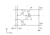
図5は、実施形態1の複数の検出領域のうち1つの検出領域を示す回路図である。図6は、実施形態1の検出領域を示す平面図である。
FIG. 5 is a circuit diagram showing one detection area among the plurality of detection areas of the first embodiment. FIG. 6 is a plan view showing the detection area of Embodiment 1. FIG.
図1に示す走査回路17は、各種制御信号に基づいて、図5及び図6に示す複数の走査線61Tx、走査線61Rxを駆動する回路である。走査回路17は、複数の超音波変換素子SEの走査線61Txを走査する駆動回路と、複数の超音波変換素子SEの走査線61Rxを走査する駆動回路と、を兼ねる。走査回路17は、複数の走査線61Tx、走査線61Rxを順次選択し、選択された走査線61Tx、走査線61Rxにゲート駆動信号を供給する。これにより、走査回路17は、走査線61Tx、走査線61Rxに接続された複数の超音波変換素子SEを選択する。なお、走査線61Tx、走査線61Rxは、アルミニウム(Al)、金、モリブデン、チタン等の金属材料が用いられる。
The scanning circuit 17 shown in FIG. 1 is a circuit that drives a plurality of scanning lines 61Tx and scanning lines 61Rx shown in FIGS. 5 and 6 based on various control signals. The scanning circuit 17 serves both as a driving circuit for scanning the scanning lines 61Tx of the plurality of ultrasonic transducers SE and as a driving circuit for scanning the scanning lines 61Rx of the plurality of ultrasonic transducers SE. The scanning circuit 17 sequentially selects a plurality of scanning lines 61Tx and 61Rx, and supplies gate drive signals to the selected scanning lines 61Tx and 61Rx. Thereby, the scanning circuit 17 selects a plurality of ultrasonic transducers SE connected to the scanning lines 61Tx and 61Rx. Note that the scanning lines 61Tx and the scanning lines 61Rx are made of metal materials such as aluminum (Al), gold, molybdenum, and titanium.
信号線選択回路16は、複数の送信信号線62Tx及び複数の受信信号線62Rxを順次又は同時に選択するスイッチ回路である。信号線選択回路16は、例えばマルチプレクサである。信号線選択回路16は、超音波処理回路40から供給される選択信号に基づいて、選択された送信信号線62Txと信号送出回路21とを接続する。信号線選択回路16は、超音波処理回路40から供給される選択信号に基づいて、選択された受信信号線62Rxと信号検出回路22とを接続する。これにより、信号線選択回路16は、超音波変換素子SEの検出信号Det(n)を信号検出回路22に出力する。なお、送信信号線62Tx及び受信信号線62Rxは、アルミニウム(Al)、金、モリブデン、チタン等の金属材料が用いられる。
The signal line selection circuit 16 is a switch circuit that sequentially or simultaneously selects a plurality of transmission signal lines 62Tx and a plurality of reception signal lines 62Rx. The signal line selection circuit 16 is, for example, a multiplexer. The signal line selection circuit 16 connects the selected transmission signal line 62Tx and the signal transmission circuit 21 based on the selection signal supplied from the ultrasonic processing circuit 40 . The signal line selection circuit 16 connects the selected reception signal line 62Rx and the signal detection circuit 22 based on the selection signal supplied from the ultrasonic processing circuit 40 . Thereby, the signal line selection circuit 16 outputs the detection signal Det(n) of the ultrasonic transducer SE to the signal detection circuit 22 . Metal materials such as aluminum (Al), gold, molybdenum, and titanium are used for the transmission signal line 62Tx and the reception signal line 62Rx.
各超音波変換素子SEは、それぞれ第1スイッチング素子Tr1、第2スイッチング素子Tr2及びメンブレン振動体UEを備えている。第1スイッチング素子Tr1は、送信信号線62Txとメンブレン振動体UEとの接続をスイッチング制御する。第2スイッチング素子Tr2は、受信信号線62Rxとメンブレン振動体UEとの接続をスイッチング制御する。
Each ultrasonic transducer SE includes a first switching element Tr1, a second switching element Tr2, and a membrane vibrator UE. The first switching element Tr1 switches and controls the connection between the transmission signal line 62Tx and the membrane vibrator UE. The second switching element Tr2 switches and controls the connection between the reception signal line 62Rx and the membrane vibrator UE.
メンブレン振動体UEの一端側の第1電極12は、第1スイッチング素子Tr1のドレイン及び第2スイッチング素子Tr2のドレインに接続され、メンブレン振動体UEの他端側の第2電極14は、基準電位GNDが供給される基準電位配線63に接続されている。図6に示すように、第1電極12は、接続配線12Wを介して、第1スイッチング素子Tr1のドレイン及び第2スイッチング素子Tr2のドレインに接続される。送信信号線62Txは、第1スイッチング素子Tr1のソースに接続されている。受信信号線62Rxは、第2スイッチング素子Tr2のソースに接続されている。そして、走査線61Txは、第1スイッチング素子Tr1のゲートに接続される。走査線61Rxは、第2スイッチング素子Tr2のゲートに接続される。なお、第1スイッチング素子Tr1及び第2スイッチング素子Tr2のドレインへの接続と、第1スイッチング素子Tr1及び第2スイッチング素子Tr2のソースへの接続は、互いに入れ替わっていてもよい。なお、基準電位配線63は、アルミニウム(Al)、金、モリブデン、チタン等の金属材料が用いられる。
The first electrode 12 on one end side of the membrane vibrating body UE is connected to the drain of the first switching element Tr1 and the drain of the second switching element Tr2, and the second electrode 14 on the other end side of the membrane vibrating body UE is connected to the reference potential. It is connected to a reference potential wiring 63 to which GND is supplied. As shown in FIG. 6, the first electrode 12 is connected to the drain of the first switching element Tr1 and the drain of the second switching element Tr2 via the connection wiring 12W. The transmission signal line 62Tx is connected to the source of the first switching element Tr1. The reception signal line 62Rx is connected to the source of the second switching element Tr2. The scanning line 61Tx is connected to the gate of the first switching element Tr1. The scanning line 61Rx is connected to the gate of the second switching element Tr2. The connection to the drain of the first switching element Tr1 and the second switching element Tr2 and the connection to the source of the first switching element Tr1 and the second switching element Tr2 may be interchanged. Note that the reference potential wiring 63 is made of a metal material such as aluminum (Al), gold, molybdenum, titanium, or the like.
図5及び図6に示す回路には、他のトランジスタ、信号増幅回路、バンドパスフィルタ、容量などがさらに含まれてもよい。
The circuits shown in FIGS. 5 and 6 may further include other transistors, signal amplifier circuits, bandpass filters, capacitors, and the like.
図7は、実施形態1において、1つの超音波変換素子の動作を示すタイミングチャートである。図7に示すように、超音波の送信と超音波の受信とは、時分割で処理される。超音波の送信では、走査回路17が選択した走査線61Txにゲート駆動信号が伝送され、信号線選択回路16は、選択した送信信号線62Txに信号送出回路21からの発振パルスSet(n)を伝送する。メンブレン振動体UEは、発振パルスSet(n)に基づいて振動し、超音波Tuを発生させる。超音波Tuの周波数は、例えば、1kHz以上1MHz以下である。
FIG. 7 is a timing chart showing the operation of one ultrasonic transducer in the first embodiment. As shown in FIG. 7, transmission of ultrasonic waves and reception of ultrasonic waves are processed in a time division manner. In transmission of ultrasonic waves, a gate drive signal is transmitted to the scanning line 61Tx selected by the scanning circuit 17, and the signal line selection circuit 16 transmits the oscillation pulse Set(n) from the signal transmission circuit 21 to the selected transmission signal line 62Tx. transmit. The membrane vibrator UE vibrates based on the oscillation pulse Set(n) to generate the ultrasonic waves Tu. The frequency of the ultrasonic wave Tu is, for example, 1 kHz or more and 1 MHz or less.
次に、走査回路17が選択した走査線61Rxにゲート駆動信号が伝送され、信号線選択回路16は、選択した受信信号線62Rxと信号検出回路22とを接続する。超音波Ruを受けて、メンブレン振動体UEは、超音波Ruを電気信号の検出信号Det(n)に変換し、検出信号Det(n)が信号検出回路22へ伝送される。なお、図示した例では、走査線61Txにゲート駆動信号が伝送されるタイミングと、走査線61Rxにゲート駆動信号が伝送されるタイミングとがずれているが、走査線61Txと走査線61Rxとにゲート駆動信号が伝送されるタイミングは同時でもよい。同時にすることで、発振パルスSet(n)と検出信号Det(n)が混線するリスクはあるが、より近い物体の検知をすることができる。
Next, a gate drive signal is transmitted to the scanning line 61Rx selected by the scanning circuit 17, and the signal line selection circuit 16 connects the selected reception signal line 62Rx and the signal detection circuit 22. Upon receiving the ultrasonic wave Ru, the membrane vibrator UE converts the ultrasonic wave Ru into a detection signal Det(n) of an electric signal, and the detection signal Det(n) is transmitted to the signal detection circuit 22 . In the illustrated example, the timing at which the gate driving signal is transmitted to the scanning line 61Tx and the timing at which the gate driving signal is transmitted to the scanning line 61Rx are shifted. The timings at which the drive signals are transmitted may be the same. By doing so at the same time, although there is a risk of crosstalk between the oscillation pulse Set(n) and the detection signal Det(n), a closer object can be detected.
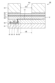
図8は、実施形態1の検出領域及び額縁領域を示す断面図である。図8では、額縁領域GAの断面とともに、検出領域AAの1つの超音波変換素子SEの断面が記載されている可撓性基板51は、可撓性を有する樹脂基板で、例えば、ポリイミド樹脂が用いられる。可撓性基板51の厚みは、1μm以上100μm以下である。
FIG. 8 is a cross-sectional view showing the detection area and the frame area of Embodiment 1. FIG. In FIG. 8, the flexible substrate 51 on which the cross section of one ultrasonic transducer SE in the detection area AA is described together with the cross section of the frame area GA is a flexible resin substrate, such as polyimide resin. Used. The thickness of the flexible substrate 51 is 1 μm or more and 100 μm or less.
フレーム層52には、超音波変換素子SE毎に、キャビティFHが開けられている。キャビティFHと平面視で重なる領域が、メンブレン振動体UEとなる。図6に示すように、平面視で、キャビティFHが第1電極12を取り囲む。
A cavity FH is opened in the frame layer 52 for each ultrasonic transducer SE. A region that overlaps with the cavity FH in plan view becomes the membrane vibrator UE. As shown in FIG. 6, the cavity FH surrounds the first electrode 12 in plan view.
フレーム層52は、例えば、ポリイミド樹脂、金属フォイルである。フレーム層52の厚みは、1μm以上100μm以下である。フレーム層52は、可撓性基板51よりも曲げにくい。例えば、フレーム層52が可撓性基板51と同じ材料である場合は、フレーム層52が可撓性基板51よりも厚いことで、第1電極12とキャビティFHに平面視で重なる可撓性基板51とが共に振動し、メンブレン振動体UEとして機能する。フレーム層52が可撓性基板51と異なる材料である場合は、可撓性基板51よりも曲げにくいフレーム層52のヤング率と厚みが設定される。
The frame layer 52 is, for example, polyimide resin or metal foil. The thickness of the frame layer 52 is 1 μm or more and 100 μm or less. The frame layer 52 is less bendable than the flexible substrate 51 . For example, when the frame layer 52 is made of the same material as the flexible substrate 51, the frame layer 52 is thicker than the flexible substrate 51, so that the flexible substrate overlaps the first electrode 12 and the cavity FH in plan view. 51 vibrate together and function as a membrane vibrator UE. When the frame layer 52 is made of a material different from that of the flexible substrate 51 , the Young's modulus and thickness of the frame layer 52 are set so that the frame layer 52 is more difficult to bend than the flexible substrate 51 .
キャビティFHは、直径φDの円形である。これにより、メンブレン振動体UEも円形となる。直径φDは、図6に示す走査線61Tx、走査線61Rx、送信信号線62Tx及び受信信号線62Rxで囲まれる範囲よりも小さい。直径φDは、例えば、0.1mm以上5mm以下である。
The cavity FH is circular with a diameter φD. As a result, the membrane vibrator UE also becomes circular. Diameter φD is smaller than the range surrounded by scanning lines 61Tx, scanning lines 61Rx, transmission signal lines 62Tx, and reception signal lines 62Rx shown in FIG. The diameter φD is, for example, 0.1 mm or more and 5 mm or less.
圧電層54は、PZT(チタン酸ジルコン酸鉛)、AlN(窒化アルミニウム)などの無機材料、ポリフッ化ビニリデン樹脂(ポリビニリデンジフロライド樹脂)などの有機材料で形成される。圧電層54の厚みは、例えば、10nm以上10000nm以下である。圧電層54には、必要に応じてバッファー層、結晶調整層、保護層、マッチング層、バッキング層などを含めてもよい。圧電層54は、検出領域AAの全体に形成されている。
The piezoelectric layer 54 is made of an inorganic material such as PZT (lead zirconate titanate) or AlN (aluminum nitride), or an organic material such as polyvinylidene fluoride resin (polyvinylidene difluoride resin). The thickness of the piezoelectric layer 54 is, for example, 10 nm or more and 10000 nm or less. The piezoelectric layer 54 may optionally include buffer layers, crystal adjustment layers, protective layers, matching layers, backing layers, and the like. The piezoelectric layer 54 is formed over the entire sensing area AA.
なお、圧電層54が形成される領域は、平面視でキャビティFHの領域と同じ大きさで、平面視でキャビティFHの領域と重ねて設けられてもよい。また、圧電層54は、平面視でキャビティFHの領域と相似形であって、キャビティFHの領域の境界よりも大きくしてもよい。あるいは、圧電層54は、平面視でキャビティFHの領域と相似形であって、キャビティFHの領域よりも小さく、第1電極12よりも大きくしてもよい。
Note that the area where the piezoelectric layer 54 is formed may have the same size as the area of the cavity FH in plan view, and may be provided so as to overlap the area of the cavity FH in plan view. In addition, the piezoelectric layer 54 may have a similar shape to the area of the cavity FH in plan view, and may be larger than the boundary of the area of the cavity FH. Alternatively, the piezoelectric layer 54 may be similar in shape to the area of the cavity FH in plan view, smaller than the area of the cavity FH, and larger than the first electrode 12 .
回路層53及び圧電層54は、ガラス基板上で形成され、回路層53及び圧電層54がガラス基板から可撓性基板51に転写される。ガラス基板上では、圧電層54が形成される。圧電層54の上には、第1電極12が形成される。第1電極12上には、第1樹脂層71が形成される。第1電極12は、例えば、アルミニウム(Al)、金、モリブデン、チタン等の金属材料が用いられる。又は、第1電極12は、これらの金属材料の少なくとも1以上を含む合金材料やこれらの金属材料の少なくとも2以上の積層体であってもよい。
The circuit layer 53 and piezoelectric layer 54 are formed on a glass substrate, and the circuit layer 53 and piezoelectric layer 54 are transferred from the glass substrate to the flexible substrate 51 . A piezoelectric layer 54 is formed on the glass substrate. A first electrode 12 is formed on the piezoelectric layer 54 . A first resin layer 71 is formed on the first electrode 12 . Metal materials such as aluminum (Al), gold, molybdenum, and titanium are used for the first electrode 12 . Alternatively, the first electrode 12 may be an alloy material containing at least one of these metal materials or a laminate of at least two of these metal materials.
ガラス基板からみて、第1樹脂層71上には、ゲート電極82が形成される。ゲート電極82の上には第2樹脂層72が積層される。第2樹脂層72の上には、ソース電極83と、ドレイン電極84とが形成される。ドレイン電極84と、第1電極12とは、スルーホール85を介して電気的に接続されている。ソース電極83及びドレイン電極84の周りの第2樹脂層72の上は、第3樹脂層73で覆われている。ソース電極83及びドレイン電極84の上には、半導体層81が形成されており、半導体層81と、ソース電極83及びドレイン電極84のそれぞれが、接合される。半導体層81、ゲート電極82、ソース電極83及びドレイン電極84は、第1スイッチング素子Tr1として機能する。ゲート電極82、ソース電極83、ドレイン電極84及びスルーホール8は、例えば、アルミニウム(Al)、金、モリブデン、チタン等の金属材料が用いられる。又は、ゲート電極82、ソース電極83、ドレイン電極84及びスルーホール85は、これらの金属材料の少なくとも1以上を含む合金材料やこれらの金属材料の少なくとも2以上の積層体であってもよい。第2スイッチング素子Tr2は、第1スイッチング素子Tr1と同じ構成であるので、詳細な説明を省略する。
A gate electrode 82 is formed on the first resin layer 71 when viewed from the glass substrate. A second resin layer 72 is laminated on the gate electrode 82 . A source electrode 83 and a drain electrode 84 are formed on the second resin layer 72 . The drain electrode 84 and the first electrode 12 are electrically connected via a through hole 85 . The second resin layer 72 around the source electrode 83 and the drain electrode 84 is covered with a third resin layer 73 . A semiconductor layer 81 is formed on the source electrode 83 and the drain electrode 84, and the semiconductor layer 81 and the source electrode 83 and the drain electrode 84 are bonded to each other. The semiconductor layer 81, gate electrode 82, source electrode 83 and drain electrode 84 function as a first switching element Tr1. The gate electrode 82, the source electrode 83, the drain electrode 84, and the through hole 8 are made of metal material such as aluminum (Al), gold, molybdenum, and titanium. Alternatively, the gate electrode 82, the source electrode 83, the drain electrode 84, and the through hole 85 may be an alloy material containing at least one of these metal materials or a laminate of at least two of these metal materials. Since the second switching element Tr2 has the same configuration as the first switching element Tr1, detailed description thereof will be omitted.
半導体層81は、酸化物半導体である。より好ましくは、半導体層81は、酸化物半導体のうち透明アモルファス酸化物半導体(TAOS:Transparent Amorphous Oxide Semiconductor)である。半導体層81に酸化物半導体を用いることにより、リーク電流が抑制される。すなわち、第1スイッチング素子Tr1または、第2スイッチング素子Tr2のうち非選択のトランジスタからのリーク電流を低減できる。このため、検出装置1は、S/N比を向上させることができる。ただし、半導体層81は、これに限定されず、微結晶酸化物半導体、アモルファス酸化物半導体、ポリシリコン、低温ポリシリコン(LTPS:Low Temperature Polycrystalline Silicone)等であってもよい。
The semiconductor layer 81 is an oxide semiconductor. More preferably, the semiconductor layer 81 is a transparent amorphous oxide semiconductor (TAOS) among oxide semiconductors. Leakage current is suppressed by using an oxide semiconductor for the semiconductor layer 81 . That is, it is possible to reduce the leak current from the non-selected transistor of the first switching element Tr1 or the second switching element Tr2. Therefore, the detection device 1 can improve the S/N ratio. However, the semiconductor layer 81 is not limited to this, and may be a microcrystalline oxide semiconductor, an amorphous oxide semiconductor, polysilicon, low temperature polysilicon (LTPS: Low Temperature Polycrystalline Silicon), or the like.
半導体層81と、第3樹脂層73の上には、第4樹脂層74が形成される。回路層53がガラス基板から可撓性基板51に転写されるので、可撓性基板51からみると、積層順は逆になる。
A fourth resin layer 74 is formed on the semiconductor layer 81 and the third resin layer 73 . Since the circuit layer 53 is transferred from the glass substrate to the flexible substrate 51, the stacking order is reversed when viewed from the flexible substrate 51. FIG.
第2樹脂層72は、窒化シリコンなどの無機絶縁膜である。第1樹脂層71、第3樹脂層73、第4樹脂層74は、無機絶縁膜でも有機絶縁膜でもよいが、例えば、アクリル樹脂などの有機絶縁膜である。第1樹脂層71、第3樹脂層73、第4樹脂層74は、有機絶縁膜であると、回路層53に亀裂が生じにくい。回路層53は、部分的に厚みを変えてもよく、例えば、第1樹脂層71、第3樹脂層73、第4樹脂層74の少なくとも1つの、平面視で重なるキャビティFHの領域の厚みを薄くしたり、除去したりしてもよい。
The second resin layer 72 is an inorganic insulating film such as silicon nitride. The first resin layer 71, the third resin layer 73, and the fourth resin layer 74 may be inorganic insulating films or organic insulating films, and are organic insulating films such as acrylic resin, for example. If the first resin layer 71, the third resin layer 73, and the fourth resin layer 74 are organic insulating films, the circuit layer 53 is less likely to crack. The thickness of the circuit layer 53 may be partially changed. It may be thinned or removed.
第1電極12が形成される圧電層54の第1面とは反対側の第2面には、第2電極14が形成されている。第2電極14は、対向電極とも呼ばれ、額縁領域GAにある基準電位配線63と、スルーホール87を介して接続される。第2電極14は、例えば、アルミニウム(Al)、金、モリブデン、チタン等の金属材料が用いられる。又は、第2電極14は、これらの金属材料の少なくとも1以上を含む合金材料やこれらの金属材料の少なくとも2以上の積層体であってもよい。
A second electrode 14 is formed on the second surface opposite to the first surface of the piezoelectric layer 54 on which the first electrode 12 is formed. The second electrode 14 is also called a counter electrode, and is connected via a through hole 87 to the reference potential wiring 63 in the frame area GA. Metal materials such as aluminum (Al), gold, molybdenum, and titanium are used for the second electrode 14 . Alternatively, the second electrode 14 may be an alloy material containing at least one of these metal materials or a laminate of at least two of these metal materials.
第2電極14は、アクリル樹脂などの有機絶縁膜の保護層55で覆われる。第2電極14は、第1電極12が接する圧電層54の面と反対側の面に接しており、圧電層54は、第1電極12と第2電極14とに挟まれる。第2電極14は、複数の超音波変換素子SEに跨がって設けられて、複数の超音波変換素子SEに共通の第2電極14となっている。これにより、第2電極14の電気抵抗が小さくなる。
The second electrode 14 is covered with a protective layer 55 of an organic insulating film such as acrylic resin. The second electrode 14 is in contact with the surface of the piezoelectric layer 54 opposite to the surface with which the first electrode 12 is in contact, and the piezoelectric layer 54 is sandwiched between the first electrode 12 and the second electrode 14 . The second electrode 14 is provided across the plurality of ultrasonic transducers SE, and serves as the second electrode 14 common to the plurality of ultrasonic transducers SE. This reduces the electrical resistance of the second electrode 14 .
可撓性基板51とフレーム層52とは、接着層56を介して接合されている。接着層56は、両面が粘着性を有しており、フレーム層52に接合された状態で、プレス加工などにより、キャビティFHが開けられている。
The flexible substrate 51 and the frame layer 52 are bonded via an adhesive layer 56 . The adhesive layer 56 has tackiness on both sides, and has a cavity FH formed by press working or the like while being bonded to the frame layer 52 .
なお、図8に示した例では転写によって超音波変換素子SEを形成しているが、その他の方法で形成されてもよい。例えば、ガラス基板上に可撓性基板51を形成し、その上に回路層53、圧電層54、第2電極14、保護層55を形成する。その後、ガラス基板から可撓性基板51を剥離し、可撓性基板51とフレーム層52とを接合してもよい。この場合、回路層53、圧電層54、第2電極14、保護層55が順次積層して形成されるため、可撓性基板51からみても積層順は逆にならない。
Although the ultrasonic transducer SE is formed by transfer in the example shown in FIG. 8, it may be formed by other methods. For example, a flexible substrate 51 is formed on a glass substrate, and a circuit layer 53, a piezoelectric layer 54, a second electrode 14, and a protective layer 55 are formed thereon. After that, the flexible substrate 51 may be separated from the glass substrate, and the flexible substrate 51 and the frame layer 52 may be bonded. In this case, since the circuit layer 53, the piezoelectric layer 54, the second electrode 14, and the protective layer 55 are sequentially laminated, the order of lamination is not reversed even when viewed from the flexible substrate 51. FIG.
第1スイッチング素子Tr1は、平面視でキャビティFHに重ならない位置に設けられ、平面視でキャビティFHに重ならない位置で、第1スイッチング素子Tr1と第1電極12とが電気的に接続されている。これにより、メンブレン振動体UEの振動により、第1スイッチング素子Tr1の劣化や第1スイッチング素子Tr1と第1電極12との接続が断線する可能性を抑制できる。
The first switching element Tr1 is provided at a position that does not overlap the cavity FH in plan view, and the first switching element Tr1 and the first electrode 12 are electrically connected at a position that does not overlap the cavity FH in plan view. . As a result, it is possible to suppress deterioration of the first switching element Tr1 and disconnection between the first switching element Tr1 and the first electrode 12 due to vibration of the membrane vibrator UE.
フレーム層52は、キャビティFHの領域をフォトレジストで覆っておき、フォトレジストの周りを塗布や成膜し、その後、フォトレジストを除去することで形成してもよい。または、フレーム層52が3Dプリントで、可撓性基板51の表面に直接形成されてもよい。
The frame layer 52 may be formed by covering the region of the cavity FH with a photoresist, coating or forming a film around the photoresist, and then removing the photoresist. Alternatively, the frame layer 52 may be 3D printed and directly formed on the surface of the flexible substrate 51 .
以上説明したように、実施形態1の検出装置1は、超音波を送受信する複数の超音波変換素子SEを含む。検出装置1は、積層体と、この積層体の第1面及び第1面の反対側の第2面のうち第1面に積層するフレーム層52と、を含む。そして、積層体は、可撓性基板51と、可撓性基板51に積層された回路層53と、回路層53に積層された圧電層54とを含む。具体的には、フレーム層52は、可撓性基板51に接合されている。超音波変換素子SEは、圧電層54に接する第1電極12と、圧電層54に接する第2電極14と、を含む。フレーム層52には、平面視して第1電極12と重なる位置に、キャビティFHがある。
As described above, the detection device 1 of Embodiment 1 includes a plurality of ultrasonic transducers SE that transmit and receive ultrasonic waves. The detection device 1 includes a laminate and a frame layer 52 laminated to a first surface of the laminate and a second surface opposite to the first surface. The laminate includes a flexible substrate 51 , a circuit layer 53 laminated on the flexible substrate 51 , and a piezoelectric layer 54 laminated on the circuit layer 53 . Specifically, the frame layer 52 is bonded to the flexible substrate 51 . The ultrasonic transducer SE includes a first electrode 12 in contact with the piezoelectric layer 54 and a second electrode 14 in contact with the piezoelectric layer 54 . The frame layer 52 has a cavity FH at a position overlapping the first electrode 12 in plan view.
この構成により、ガラスやシリコンなどの基板よりも可撓性基板51の方が振動に応じて撓みやすいので、可撓性基板51、回路層53及び圧電層54の接合面の破壊が生じにくい。また、可撓性基板51と、キャビティFHがあるフレーム層52とを貼り合わせるだけで、メンブレン振動体UEを安価に製造することができる。
With this configuration, the flexible substrate 51 bends more easily in response to vibration than a substrate made of glass, silicon, or the like, so that the bonding surfaces of the flexible substrate 51, the circuit layer 53, and the piezoelectric layer 54 are less likely to break. Further, the membrane vibrator UE can be manufactured at low cost only by bonding the flexible substrate 51 and the frame layer 52 having the cavity FH.
(実施形態2)
図9は、実施形態2の検出領域を示す断面図である。実施形態2では、実施形態1と同じ構成については同じ符号を付して、説明を省略することがある。図9では、検出領域AAの1つの超音波変換素子SEの断面が記載されている。 (Embodiment 2)
FIG. 9 is a cross-sectional view showing the detection area of Embodiment 2. FIG. In the second embodiment, the same reference numerals are assigned to the same configurations as in the first embodiment, and the description may be omitted. In FIG. 9, a cross-section of one ultrasonic transducer SE of the detection area AA is shown.
実施形態1では、可撓性基板51の一面に、フレーム層52が接合されているが、実施形態2では、フレーム層52が回路層53及び圧電層54に対して、実施形態1の反対側にある。
In the first embodiment, the frame layer 52 is bonded to one surface of the flexible substrate 51, but in the second embodiment, the frame layer 52 is attached to the circuit layer 53 and the piezoelectric layer 54 on the opposite side of the first embodiment. It is in.
保護層55の一面に、フレーム層52が接着層56を介して接合されている。フレーム層52には、超音波変換素子SE毎に、キャビティFHが開けられている。
The frame layer 52 is bonded to one surface of the protective layer 55 via an adhesive layer 56 . A cavity FH is opened in the frame layer 52 for each ultrasonic transducer SE.
以上説明したように、実施形態2の検出装置1は、超音波を送受信する複数の超音波変換素子SEを含む。検出装置1は、積層体と、この積層体の第1面及び第1面の反対側の第2面のうち第2面に積層するフレーム層52と、を含む。そして、積層体は、可撓性基板51と、可撓性基板51に積層された回路層53と、回路層53に積層された圧電層54とを含む。具体的には、フレーム層52は、積層体の可撓性基板51がある側とは反対側の保護層55に接合されている。超音波変換素子SEは、圧電層54に接する第1電極12と、圧電層54に接する第2電極14と、を含む。フレーム層52には、平面視して第1電極12と重なる位置に、キャビティFHがある。
As described above, the detection device 1 of Embodiment 2 includes a plurality of ultrasonic transducers SE that transmit and receive ultrasonic waves. The detection device 1 includes a laminate and a frame layer 52 laminated to the second of the first side of the laminate and the second side opposite to the first side. The laminate includes a flexible substrate 51 , a circuit layer 53 laminated on the flexible substrate 51 , and a piezoelectric layer 54 laminated on the circuit layer 53 . Specifically, the frame layer 52 is bonded to a protective layer 55 on the opposite side of the laminate from the flexible substrate 51 . The ultrasonic transducer SE includes a first electrode 12 in contact with the piezoelectric layer 54 and a second electrode 14 in contact with the piezoelectric layer 54 . The frame layer 52 has a cavity FH at a position overlapping the first electrode 12 in plan view.
この構成により、ガラスやシリコンなどの基板よりも可撓性基板51の方が振動に応じて撓みやすいので、可撓性基板51、回路層53及び圧電層54の接合面の破壊が生じにくい。また、可撓性基板51と、キャビティFHがあるフレーム層52とを貼り合わせるだけで、メンブレン振動体UEを安価に製造することができる。
With this configuration, the flexible substrate 51 bends more easily in response to vibration than a substrate made of glass, silicon, or the like, so that the bonding surfaces of the flexible substrate 51, the circuit layer 53, and the piezoelectric layer 54 are less likely to break. Further, the membrane vibrator UE can be manufactured at low cost only by bonding the flexible substrate 51 and the frame layer 52 having the cavity FH.
また、フレーム層52が、実施形態1よりも回路層53及び圧電層54に近いので、1つの超音波変換素子SEの圧電層54の振動が隣接する超音波変換素子SEに伝搬するクロストークが抑制される。
In addition, since the frame layer 52 is closer to the circuit layer 53 and the piezoelectric layer 54 than in the first embodiment, crosstalk in which the vibration of the piezoelectric layer 54 of one ultrasonic transducer SE propagates to the adjacent ultrasonic transducer SE occurs. Suppressed.
(実施形態3)
図10は、実施形態3の検出領域を示す断面図である。実施形態3では、実施形態1及び実施形態2と同じ構成については同じ符号を付して、説明を省略することがある。図10では、検出領域AAの1つの超音波変換素子SEの断面が記載されている。 (Embodiment 3)
FIG. 10 is a cross-sectional view showing the detection area of Embodiment 3. FIG. In the third embodiment, the same reference numerals are assigned to the same configurations as in the first and second embodiments, and the description thereof may be omitted. FIG. 10 shows a cross section of one ultrasonic transducer SE of the detection area AA.
可撓性基板51の一面に、フレーム層52Aが接着層56Aを介して接合されている。フレーム層52Aには、超音波変換素子SE毎に、キャビティFHAが開けられている。
A frame layer 52A is bonded to one surface of the flexible substrate 51 via an adhesive layer 56A. A cavity FHA is opened in the frame layer 52A for each ultrasonic transducer SE.
保護層55の一面に、フレーム層52Bが接着層56Bを介して接合されている。フレーム層52Bには、超音波変換素子SE毎に、キャビティFHBが開けられている。
A frame layer 52B is bonded to one surface of the protective layer 55 via an adhesive layer 56B. A cavity FHB is opened in the frame layer 52B for each ultrasonic transducer SE.
以上説明したように、実施形態3の検出装置1は、超音波を送受信する複数の超音波変換素子SEを含む。検出装置1は、積層体と、この積層体の第1面に積層するフレーム層52A及び第1面の反対側の第2面に積層するフレーム層52Bと、を含む。そして、積層体は、可撓性基板51と、可撓性基板51に積層された回路層53と、回路層53に積層された圧電層54とを含む。具体的には、回路層53及び圧電層54は、フレーム層52Aとフレーム層52Bとに挟まれている。超音波変換素子SEは、圧電層54に接する第1電極12と、圧電層54に接する第2電極14と、を含む。フレーム層52には、平面視して第1電極12と重なる位置に、キャビティFHA、キャビティFHBがある。そして、一方のフレーム層52AのキャビティFHAと、他方のフレーム層52BのキャビティFHBとが平面視で重なる位置にある。
As described above, the detection device 1 of Embodiment 3 includes a plurality of ultrasonic transducers SE that transmit and receive ultrasonic waves. The detection device 1 includes a laminate, a frame layer 52A laminated on a first side of the laminate, and a frame layer 52B laminated on a second side opposite to the first side. The laminate includes a flexible substrate 51 , a circuit layer 53 laminated on the flexible substrate 51 , and a piezoelectric layer 54 laminated on the circuit layer 53 . Specifically, the circuit layer 53 and the piezoelectric layer 54 are sandwiched between the frame layers 52A and 52B. The ultrasonic transducer SE includes a first electrode 12 in contact with the piezoelectric layer 54 and a second electrode 14 in contact with the piezoelectric layer 54 . The frame layer 52 has a cavity FHA and a cavity FHB at positions overlapping the first electrode 12 in plan view. The cavity FHA of one frame layer 52A and the cavity FHB of the other frame layer 52B are positioned to overlap each other in plan view.
この構成により、ガラスやシリコンなどの基板よりも可撓性基板51の方が振動に応じて撓みやすいので、可撓性基板51、回路層53及び圧電層54の接合面の破壊が生じにくい。また、可撓性基板51と、キャビティFHがあるフレーム層52とを貼り合わせるだけで、メンブレン振動体UEを安価に製造することができる。
With this configuration, the flexible substrate 51 bends more easily in response to vibration than a substrate made of glass, silicon, or the like, so that the bonding surfaces of the flexible substrate 51, the circuit layer 53, and the piezoelectric layer 54 are less likely to break. Further, the membrane vibrator UE can be manufactured at low cost only by bonding the flexible substrate 51 and the frame layer 52 having the cavity FH.
回路層53及び圧電層54は、フレーム層52Aとフレーム層52Bとに挟まれているので、1つの超音波変換素子SEの圧電層54の振動が隣接する超音波変換素子SEに伝搬するクロストークが抑制される。
Since the circuit layer 53 and the piezoelectric layer 54 are sandwiched between the frame layer 52A and the frame layer 52B, the vibration of the piezoelectric layer 54 of one ultrasonic transducer SE propagates to the adjacent ultrasonic transducer SE. is suppressed.
(実施形態4)
図11は、実施形態4の検出領域を示す断面図である。実施形態4では、実施形態1から実施形態3と同じ構成については同じ符号を付して、説明を省略することがある。図11では、検出領域AAの1つの超音波変換素子SEの断面が記載されている。 (Embodiment 4)
FIG. 11 is a cross-sectional view showing the detection area of the fourth embodiment. In the fourth embodiment, the same reference numerals are assigned to the same configurations as in the first to third embodiments, and the description thereof may be omitted. FIG. 11 shows a cross-section of one ultrasonic transducer SE of the detection area AA.
図11に示すように、基準電位配線63が各超音波変換素子SEに引き回されている。基準電位配線63は、ソース電極83及びドレイン電極84とは異なる層に形成されており、例えば、半導体層81と同層に形成されている。
As shown in FIG. 11, a reference potential wiring 63 is routed to each ultrasonic transducer SE. The reference potential wiring 63 is formed in a layer different from that of the source electrode 83 and the drain electrode 84, and is formed in the same layer as the semiconductor layer 81, for example.
第1電極12と同層の中継配線88は、基準電位配線63とスルーホール87Aを介して接続されている。第2電極14と、中継配線88とは、スルーホール89を介して接続されている。これにより、額縁領域GAが狭くできる。
A relay wiring 88 in the same layer as the first electrode 12 is connected to the reference potential wiring 63 via a through hole 87A. The second electrode 14 and the relay wiring 88 are connected via a through hole 89 . Thereby, the frame area GA can be narrowed.
各超音波変換素子SEの第2電極14は、キャビティFHと平面視で重なる領域にそれぞれ設けられている。隣接する第2電極14は、互いに分離されているので、隣接する超音波変換素子SEが検出する超音波Ruのクロストークが低減する。
The second electrode 14 of each ultrasonic transducer SE is provided in a region overlapping the cavity FH in plan view. Since adjacent second electrodes 14 are separated from each other, crosstalk of ultrasonic waves Ru detected by adjacent ultrasonic transducer elements SE is reduced.
平面視でキャビティFHに重ならない位置において、第2電極14と基準電位配線63とが電気的に接続されているので、基準電位配線63の断線の可能性が低くなる。
Since the second electrode 14 and the reference potential wiring 63 are electrically connected at a position not overlapping the cavity FH in plan view, the possibility of disconnection of the reference potential wiring 63 is reduced.
(実施形態5)
図12は、実施形態5の検出領域を示す断面図である。図13は、実施形態5の複数の検出領域のうち1つの検出領域を示す回路図である。実施形態4では、実施形態1から実施形態4と同じ構成については同じ符号を付して、説明を省略することがある。図12では、検出領域AAの1つの超音波変換素子SEの断面が記載されている。 (Embodiment 5)
FIG. 12 is a cross-sectional view showing the detection area of the fifth embodiment. FIG. 13 is a circuit diagram showing one detection area among a plurality of detection areas according to the fifth embodiment. In the fourth embodiment, the same reference numerals are assigned to the same configurations as in the first to fourth embodiments, and the description thereof may be omitted. FIG. 12 shows a cross-section of one ultrasonic transducer SE of the detection area AA.
図12に示すように、第2電極14は、第3スイッチング素子Tr3に電気的に接続されている。第3スイッチング素子Tr3は、第1スイッチング素子Tr1と同じ構成であるので、詳細な説明を省略する。第3スイッチング素子Tr3のドレイン電極84と、第2電極14とは、スルーホール85、中継配線88、スルーホール89を介して電気的に接続されている。
As shown in FIG. 12, the second electrode 14 is electrically connected to the third switching element Tr3. Since the third switching element Tr3 has the same configuration as the first switching element Tr1, detailed description thereof will be omitted. The drain electrode 84 of the third switching element Tr3 and the second electrode 14 are electrically connected via a through hole 85, a relay wiring 88 and a through hole 89. As shown in FIG.
各超音波変換素子SEは、それぞれ第1スイッチング素子Tr1、第2スイッチング素子Tr2、第3スイッチング素子Tr3、第4スイッチング素子Tr4及びメンブレン振動体UEを備えている。第1スイッチング素子Tr1は、送信信号線62Txとメンブレン振動体UEとの接続をスイッチング制御する。第2スイッチング素子Tr2は、受信信号線62Rxとメンブレン振動体UEとの接続をスイッチング制御する。第3スイッチング素子Tr3は、送信信号線62Txxとメンブレン振動体UEとの接続をスイッチング制御する。第2スイッチング素子Tr2は、基準電位配線63とメンブレン振動体UEとの接続をスイッチング制御する。
Each ultrasonic transducer SE includes a first switching element Tr1, a second switching element Tr2, a third switching element Tr3, a fourth switching element Tr4, and a membrane vibrator UE. The first switching element Tr1 switches and controls the connection between the transmission signal line 62Tx and the membrane vibrator UE. The second switching element Tr2 switches and controls the connection between the reception signal line 62Rx and the membrane vibrator UE. The third switching element Tr3 switches and controls the connection between the transmission signal line 62Txx and the membrane vibrator UE. The second switching element Tr2 switches and controls the connection between the reference potential wiring 63 and the membrane vibrator UE.
第2電極14は、第3スイッチング素子Tr3のドレインに接続されている。送信信号線62Txxは、第3スイッチング素子Tr3のソースに接続されている。送信信号線62Txx(第2送信信号線)には、送信信号線62Tx(第1送信信号線)の発振パルスSet(n)の逆相の信号が伝送される。また、第2電極14は、第4スイッチング素子Tr4のドレインに接続されている。基準電位配線63は、第4スイッチング素子Tr4のソースに接続されている。
The second electrode 14 is connected to the drain of the third switching element Tr3. The transmission signal line 62Txx is connected to the source of the third switching element Tr3. A signal opposite in phase to the oscillation pulse Set(n) of the transmission signal line 62Tx (first transmission signal line) is transmitted to the transmission signal line 62Txx (second transmission signal line). Also, the second electrode 14 is connected to the drain of the fourth switching element Tr4. The reference potential wiring 63 is connected to the source of the fourth switching element Tr4.
超音波送信時では、第1スイッチング素子Tr1及び第3スイッチング素子Tr3は、同時にオン動作し、第2スイッチング素子Tr2及び第4スイッチング素子Tr4は、同時にオフ動作する。送信信号線62Txが、第1スイッチング素子Tr1を介して第1電極12に、発振パルスSet(n)の信号を伝送し、送信信号線62Txxが、第3スイッチング素子Tr3を介して第2電極14に、発振パルスSet(n)の逆相の信号を伝送する。その結果、圧電層54に印加される信号の振幅が実施形態1の倍となり、超音波の出力が向上する。
During ultrasonic wave transmission, the first switching element Tr1 and the third switching element Tr3 are simultaneously turned on, and the second switching element Tr2 and the fourth switching element Tr4 are simultaneously turned off. The transmission signal line 62Tx transmits the signal of the oscillation pulse Set(n) to the first electrode 12 via the first switching element Tr1, and the transmission signal line 62Txx transmits the signal to the second electrode 14 via the third switching element Tr3. , a signal opposite in phase to the oscillation pulse Set(n) is transmitted. As a result, the amplitude of the signal applied to the piezoelectric layer 54 is double that of the first embodiment, and the ultrasonic output is improved.
超音波受信時では、第1スイッチング素子Tr1及び第3スイッチング素子Tr3は、同時にオフ動作し、第2スイッチング素子Tr2及び第4スイッチング素子Tr4は、同時にオン動作する。受信信号線62Rxと第1電極12とが、第2スイッチング素子Tr2を介して接続され、基準電位配線63と第2電極14とが、第3スイッチング素子Tr3を介して接続される。その結果、超音波変換素子SEの検出信号Det(n)が信号検出回路22に出力される。
When receiving ultrasonic waves, the first switching element Tr1 and the third switching element Tr3 are simultaneously turned off, and the second switching element Tr2 and the fourth switching element Tr4 are simultaneously turned on. The reception signal line 62Rx and the first electrode 12 are connected via the second switching element Tr2, and the reference potential wiring 63 and the second electrode 14 are connected via the third switching element Tr3. As a result, the detection signal Det(n) of the ultrasonic transducer SE is output to the signal detection circuit 22 .
各超音波変換素子SEの第2電極14は、キャビティFHと平面視で重なる領域にそれぞれ設けられている。隣接する第2電極14は、互いに分離されている。走査回路17が選択していない超音波変換素子SEでは、第2電極14が基準電位GNDとなり、走査回路17が選択していない超音波変換素子SEからのノイズが抑制される。
The second electrode 14 of each ultrasonic transducer SE is provided in a region overlapping the cavity FH in plan view. Adjacent second electrodes 14 are separated from each other. In the ultrasonic transducers SE not selected by the scanning circuit 17, the second electrode 14 becomes the reference potential GND, and noise from the ultrasonic transducers SE not selected by the scanning circuit 17 is suppressed.
走査回路17が選択している超音波変換素子SEでは、第2電極14に、発振パルスSet(n)の逆走の信号が伝送されるため、メンブレン振動体UEの振幅が大きくなる。走査回路17が選択していない超音波変換素子SEでは、第2電極14が基準電位GNDとなり、他の超音波変換素子SEの振動の影響を抑制できる。
In the ultrasonic transducer SE selected by the scanning circuit 17, the reverse running signal of the oscillation pulse Set(n) is transmitted to the second electrode 14, so the amplitude of the membrane vibrator UE increases. In the ultrasonic transducers SE not selected by the scanning circuit 17, the second electrode 14 becomes the reference potential GND, and the influence of the vibration of the other ultrasonic transducers SE can be suppressed.
(実施形態6)
図14は、実施形態6の検出領域を示す断面図である。図15は、実施形態6の第1電極及び第2電極を示す平面図である。図14は、図15のXIV-XIV断面である。実施形態6では、実施形態1から実施形態5と同じ構成については同じ符号を付して、説明を省略することがある。図14では、検出領域AAの1つの超音波変換素子SEの断面が記載されている。 (Embodiment 6)
FIG. 14 is a cross-sectional view showing the detection area of Embodiment 6. FIG. 15 is a plan view showing the first electrode and the second electrode of Embodiment 6. FIG. FIG. 14 is the XIV-XIV cross section of FIG. In Embodiment 6, the same components as inEmbodiments 1 to 5 are denoted by the same reference numerals, and description thereof may be omitted. FIG. 14 shows a cross-section of one ultrasonic transducer SE of the detection area AA.
図14は、実施形態6の検出領域を示す断面図である。図15は、実施形態6の第1電極及び第2電極を示す平面図である。図14は、図15のXIV-XIV断面である。実施形態6では、実施形態1から実施形態5と同じ構成については同じ符号を付して、説明を省略することがある。図14では、検出領域AAの1つの超音波変換素子SEの断面が記載されている。 (Embodiment 6)
FIG. 14 is a cross-sectional view showing the detection area of Embodiment 6. FIG. 15 is a plan view showing the first electrode and the second electrode of Embodiment 6. FIG. FIG. 14 is the XIV-XIV cross section of FIG. In Embodiment 6, the same components as in
図14に示すように、基準電位配線63が各超音波変換素子SEに引き回されている。基準電位配線63は、ソース電極83及びドレイン電極84とは異なる層に形成されており、例えば、半導体層81と同層に形成されている。
As shown in FIG. 14, a reference potential wiring 63 is routed to each ultrasonic transducer SE. The reference potential wiring 63 is formed in a layer different from that of the source electrode 83 and the drain electrode 84, and is formed in the same layer as the semiconductor layer 81, for example.
第1電極12と同層の第2電極14は、基準電位配線63とスルーホール87Bを介して接続されている。図15に示すように、第2電極14は、第1電極12が接する圧電層54の面と同じ側の面に接している。そして、第2電極14は、第2電極14の内側にある。これにより、額縁領域GAが狭くできる。
The second electrode 14 in the same layer as the first electrode 12 is connected to the reference potential wiring 63 via the through hole 87B. As shown in FIG. 15, the second electrode 14 is in contact with the same side of the piezoelectric layer 54 as the first electrode 12 is in contact with. And the second electrode 14 is inside the second electrode 14 . Thereby, the frame area GA can be narrowed.
各超音波変換素子SEの第2電極14は、キャビティFHと平面視で重なる領域にそれぞれ設けられている。隣接する第2電極14は、互いに分離されているので、隣接する超音波変換素子SEが検出する超音波Ruのクロストークが低減する。
The second electrode 14 of each ultrasonic transducer SE is provided in a region overlapping the cavity FH in plan view. Since adjacent second electrodes 14 are separated from each other, crosstalk of ultrasonic waves Ru detected by adjacent ultrasonic transducer elements SE is reduced.
第2電極14が形成される領域は、平面視でキャビティFHの領域と相似形であって、キャビティFHの領域よりも小さい。第1電極12が形成される領域は、平面視で、キャビティFHの領域の境界と重なり、第1電極12は、円環状である。
The area where the second electrode 14 is formed has a similar shape to the area of the cavity FH in plan view and is smaller than the area of the cavity FH. The area where the first electrode 12 is formed overlaps with the boundary of the area of the cavity FH in plan view, and the first electrode 12 has an annular shape.
図16は、実施形態6の変形例1に係る第1電極及び第2電極を示す平面図である。図16に示すように、変形例1では、第2電極14が矩形であり、第1電極12の外径が矩形で、環状である。なお、第1電極12と第2電極14とは、実施形態6と同層である。
16 is a plan view showing the first electrode and the second electrode according to Modification 1 of Embodiment 6. FIG. As shown in FIG. 16, in Modification 1, the second electrode 14 is rectangular, and the outer diameter of the first electrode 12 is rectangular and annular. The first electrode 12 and the second electrode 14 are the same layer as in the sixth embodiment.
図17は、実施形態6の変形例2に係る第1電極及び第2電極を示す平面図である。図17に示すように、変形例2では、第2電極14が形成される領域が、平面視でキャビティFHの領域と相似形であって、キャビティFHの領域よりも小さい。第1電極12が形成される領域は、平面視で、キャビティFHの領域の境界と重なり、第1電極12は、円環状である。なお、第1電極12と第2電極14とは、実施形態6と同様に同層である。
17 is a plan view showing a first electrode and a second electrode according to Modification 2 of Embodiment 6. FIG. As shown in FIG. 17, in Modification 2, the region where the second electrode 14 is formed is similar in shape to the region of the cavity FH in plan view, and is smaller than the region of the cavity FH. The area where the first electrode 12 is formed overlaps with the boundary of the area of the cavity FH in plan view, and the first electrode 12 has an annular shape. Note that the first electrode 12 and the second electrode 14 are the same layer as in the sixth embodiment.
第1電極12よりも外側の位置に、スルーホール87Bが配置されており、スルーホール87Bと第2電極14とが配線で接続されている。これにより、基準電位配線63が平面視でキャビティFHの領域と重なる領域と重ならなくなることから、基準電位配線63がメンブレン振動体UEの振動の影響を受けにくくなり、検出装置1の信頼性が向上する。
A through hole 87B is arranged outside the first electrode 12, and the through hole 87B and the second electrode 14 are connected by wiring. As a result, the reference potential wiring 63 does not overlap with the region overlapping the cavity FH region in plan view, so that the reference potential wiring 63 is less susceptible to the vibration of the membrane vibrating body UE, and the reliability of the detection device 1 is improved. improves.
図18は、実施形態6の変形例3に係る第1電極及び第2電極を示す平面図である。図18に示すように、変形例3では、第1電極12及び第2電極14が矩形であり、第1電極12及び第2電極14が互いに隣接する。なお、第1電極12と第2電極14とは、実施形態6と同様に同層である。
18 is a plan view showing a first electrode and a second electrode according to Modification 3 of Embodiment 6. FIG. As shown in FIG. 18, in Modification 3, the first electrode 12 and the second electrode 14 are rectangular, and the first electrode 12 and the second electrode 14 are adjacent to each other. Note that the first electrode 12 and the second electrode 14 are the same layer as in the sixth embodiment.
平面視でキャビティFHの領域と重なる領域よりも外側の位置に、スルーホール87Bが配置されており、スルーホール87Bと第2電極14とが配線で接続されている。これにより、基準電位配線63が平面視でキャビティFHの領域と重なる領域と重ならなくなることから、基準電位配線63がメンブレン振動体UEの振動の影響を受けにくくなり、検出装置1の信頼性が向上する。
A through-hole 87B is arranged at a position outside an area overlapping with the area of the cavity FH in plan view, and the through-hole 87B and the second electrode 14 are connected by wiring. As a result, the reference potential wiring 63 does not overlap with the region overlapping the cavity FH region in plan view, so that the reference potential wiring 63 is less susceptible to the vibration of the membrane vibrating body UE, and the reliability of the detection device 1 is improved. improves.
図19は、実施形態6の変形例4に係る第1電極及び第2電極を示す平面図である。図19に示すように、変形例4では、第1電極12及び第2電極14が互いにかみ合う櫛歯電極である。なお、第1電極12と第2電極14とは、実施形態6と同様に同層である。
19 is a plan view showing a first electrode and a second electrode according to Modification 4 of Embodiment 6. FIG. As shown in FIG. 19, in Modification 4, the first electrode 12 and the second electrode 14 are interdigitated comb electrodes. Note that the first electrode 12 and the second electrode 14 are the same layer as in the sixth embodiment.
平面視でキャビティFHの領域と重なる領域よりも外側の位置に、スルーホール87Bが配置されており、スルーホール87Bと第2電極14とが配線で接続されている。これにより、基準電位配線63が平面視でキャビティFHの領域と重なる領域と重ならなくなることから、基準電位配線63がメンブレン振動体UEの振動の影響を受けにくくなり、検出装置1の信頼性が向上する。
A through-hole 87B is arranged at a position outside an area overlapping with the area of the cavity FH in plan view, and the through-hole 87B and the second electrode 14 are connected by wiring. As a result, the reference potential wiring 63 does not overlap with the region overlapping the cavity FH region in plan view, so that the reference potential wiring 63 is less susceptible to the vibration of the membrane vibrating body UE, and the reliability of the detection device 1 is improved. improves.
(実施形態7)
図20は、実施形態7の検出領域を示す平面図である。図21は、実施形態7の検出領域を示す断面図である。図20は、図21のXX-XX’断面である。実施形態7では、実施形態1から実施形態6と同じ構成については同じ符号を付して、説明を省略することがある。図20では、検出領域AAの1つの超音波変換素子SEの断面が記載されている。 (Embodiment 7)
FIG. 20 is a plan view showing the detection area of Embodiment 7. FIG. FIG. 21 is a cross-sectional view showing the detection area of Embodiment 7. FIG. FIG. 20 is the XX-XX' section of FIG. In Embodiment 7, the same components as inEmbodiments 1 to 6 are denoted by the same reference numerals, and description thereof may be omitted. In FIG. 20, a cross section of one ultrasonic transducer SE of the detection area AA is shown.
図20は、実施形態7の検出領域を示す平面図である。図21は、実施形態7の検出領域を示す断面図である。図20は、図21のXX-XX’断面である。実施形態7では、実施形態1から実施形態6と同じ構成については同じ符号を付して、説明を省略することがある。図20では、検出領域AAの1つの超音波変換素子SEの断面が記載されている。 (Embodiment 7)
FIG. 20 is a plan view showing the detection area of Embodiment 7. FIG. FIG. 21 is a cross-sectional view showing the detection area of Embodiment 7. FIG. FIG. 20 is the XX-XX' section of FIG. In Embodiment 7, the same components as in
実施形態7では、1つの超音波変換素子SEについて、第1電極12Txと第1電極12Rxとが配置されている。第1電極12Txは、超音波Tuを生成する超音波送信用の電極であり、第1電極12Rxは、超音波Ruを受ける超音波受信用の電極である。
In Embodiment 7, the first electrode 12Tx and the first electrode 12Rx are arranged for one ultrasonic transducer SE. The first electrode 12Tx is an ultrasonic transmitting electrode that generates an ultrasonic wave Tu, and the first electrode 12Rx is an ultrasonic receiving electrode that receives an ultrasonic wave Ru.
各超音波変換素子SEは、それぞれ第1スイッチング素子Tr1、第2スイッチング素子Tr2、メンブレン振動体UETx、及びメンブレン振動体UERxを備えている。第1スイッチング素子Tr1と、第1電極12Txとは、スルーホール85Txを介して電気的に接続されている。第1スイッチング素子Tr1は、送信信号線62Txとメンブレン振動体UETxとの接続をスイッチング制御する。第2スイッチング素子Tr2と、第1電極12Rxとは、スルーホール85Rxを介して電気的に接続されている。第2スイッチング素子Tr2は、受信信号線62Rxとメンブレン振動体UERxとの接続をスイッチング制御する。
Each ultrasonic transducer SE includes a first switching element Tr1, a second switching element Tr2, a membrane oscillator UETx, and a membrane oscillator UERx. The first switching element Tr1 and the first electrode 12Tx are electrically connected via a through hole 85Tx. The first switching element Tr1 switches and controls the connection between the transmission signal line 62Tx and the membrane vibrator UETx. The second switching element Tr2 and the first electrode 12Rx are electrically connected via a through hole 85Rx. The second switching element Tr2 switches and controls the connection between the reception signal line 62Rx and the membrane vibrator UERx.
フレーム層52には、超音波変換素子SE毎に、第1キャビティFHTx、第2キャビティFHRxが開けられている。フレーム層52には、平面視して一方の第1電極12Txと重なる位置に、第1キャビティFHTxがあり、他方の第1電極12Rxと重なる位置に、第2キャビティFHRxがある。そして、第1キャビティFHTxと平面視で重なる領域が、メンブレン振動体UETxとなる。第2キャビティFHRxと平面視で重なる領域が、メンブレン振動体UERxとなる。
A first cavity FHTx and a second cavity FHRx are opened in the frame layer 52 for each ultrasonic transducer SE. The frame layer 52 has a first cavity FHTx at a position overlapping with one of the first electrodes 12Tx in plan view, and a second cavity FHRx at a position overlapping with the other first electrode 12Rx. A region that overlaps with the first cavity FHTx in plan view becomes the membrane vibrator UETx. A region that overlaps with the second cavity FHRx in plan view becomes the membrane vibrator UERx.
超音波の送信と超音波の受信とは、時分割で処理される。実施形態7では、メンブレン振動体UETxと、メンブレン振動体UERxとを分けて動作させているので、超音波の送信から超音波の受信へ切り替える切り替え時間を短くしても、メンブレン振動体UETxからメンブレン振動体UERxが受ける影響が少ない。その結果、検出装置1は、検出サイクルが短くなり、検出精度が向上する。
Ultrasonic wave transmission and ultrasonic wave reception are processed in a time-division manner. In Embodiment 7, the membrane vibrating body UETx and the membrane vibrating body UERx are operated separately. The vibrator UERx is less affected. As a result, the detection device 1 has a shorter detection cycle and improved detection accuracy.
なお、第1列の超音波変換素子SEには、第1電極12Txが配置され、第2列の超音波変換素子SEには、第1電極12Rxが配置されていてもよい。
The first electrode 12Tx may be arranged on the first row of ultrasonic transducer elements SE, and the first electrode 12Rx may be arranged on the second row of ultrasonic transducer elements SE.
以上、本開示の好適な実施の形態を説明したが、本開示このような実施の形態に限定されるものではない。実施の形態で開示された内容はあくまで一例にすぎず、本開示の趣旨を逸脱しない範囲で種々の変更が可能である。例えば、実施の形態では、送受信兼用の超音波変換素子で記載しているが、送信専用もしくは受信専用の超音波変換素子にも適用できる。本開示の趣旨を逸脱しない範囲で行われた適宜の変更についても、当然に本開示の技術的範囲に属する。
Although the preferred embodiments of the present disclosure have been described above, the present disclosure is not limited to such embodiments. The content disclosed in the embodiment is merely an example, and various modifications are possible without departing from the gist of the present disclosure. For example, in the embodiments, ultrasonic transducers for both transmission and reception are described, but ultrasonic transducers for transmission and reception are also applicable. Appropriate changes that do not deviate from the spirit of the present disclosure also naturally belong to the technical scope of the present disclosure.
1 検出装置
10 超音波変換アレイ
12、12Rx、12Tx 第1電極
12W 接続配線
14 第2電極
16 信号線選択回路
17 走査回路
20 制御部
21 信号送出回路
22 信号検出回路
51 可撓性基板
52、52A、52B フレーム層
53 回路層
54 圧電層
55 保護層
56、56A、56B 接着層
61Rx、61Tx 走査線
62Rx 受信信号線
62Tx、62Txx 送信信号線
63 基準電位配線
200 表示パネル
AA 検出領域
F 被検出体
FH、FHA、FHB キャビティ
FHTx 第1キャビティ
FHRx 第2キャビティ
GA 額縁領域
UE、UERx、UETx メンブレン振動体 1detection device 10 ultrasonic transducer array 12, 12Rx, 12Tx first electrode 12W connection wiring 14 second electrode 16 signal line selection circuit 17 scanning circuit 20 control unit 21 signal transmission circuit 22 signal detection circuit 51 flexible substrates 52, 52A , 52B Frame layer 53 Circuit layer 54 Piezoelectric layer 55 Protective layers 56, 56A, 56B Adhesive layers 61Rx, 61Tx Scanning line 62Rx Receiving signal lines 62Tx, 62Txx Transmitting signal line 63 Reference potential wiring 200 Display panel AA Detection area F Object to be detected FH , FHA, FHB Cavity FHTx First cavity FHRx Second cavity GA Frame region UE, UERx, UETx Membrane vibrator
10 超音波変換アレイ
12、12Rx、12Tx 第1電極
12W 接続配線
14 第2電極
16 信号線選択回路
17 走査回路
20 制御部
21 信号送出回路
22 信号検出回路
51 可撓性基板
52、52A、52B フレーム層
53 回路層
54 圧電層
55 保護層
56、56A、56B 接着層
61Rx、61Tx 走査線
62Rx 受信信号線
62Tx、62Txx 送信信号線
63 基準電位配線
200 表示パネル
AA 検出領域
F 被検出体
FH、FHA、FHB キャビティ
FHTx 第1キャビティ
FHRx 第2キャビティ
GA 額縁領域
UE、UERx、UETx メンブレン振動体 1
Claims (17)
- 超音波を送受信する複数の超音波変換素子を含む検出装置であって、
可撓性基板と、
複数の第1電極及び少なくとも1つの第2電極を含み、かつ前記可撓性基板に積層された回路層と、
前記回路層に積層された圧電層と、
を含む積層体と、
前記積層体の第1面及び前記第1面の反対側の第2面の少なくとも1つの面に積層するフレーム層と、を含み、
1つの前記超音波変換素子は、
前記圧電層に接する少なくとも1つの前記第1電極と、
前記圧電層に接する少なくとも1つの前記第2電極と、を含み、
前記フレーム層には、平面視して前記第1電極と重なる位置に、キャビティがある、
検出装置。 A detection device including a plurality of ultrasonic transducers that transmit and receive ultrasonic waves,
a flexible substrate;
a circuit layer including a plurality of first electrodes and at least one second electrode and laminated to the flexible substrate;
a piezoelectric layer laminated on the circuit layer;
a laminate comprising
a frame layer laminated to at least one of a first side of the laminate and a second side opposite the first side;
One said ultrasonic transducer,
at least one first electrode in contact with the piezoelectric layer;
at least one second electrode in contact with the piezoelectric layer;
The frame layer has a cavity at a position overlapping with the first electrode in plan view,
detection device. - 前記第2電極は、前記第1電極が接する前記圧電層の面と反対側の前記圧電層の面に接しており、前記圧電層は、前記第1電極と前記第2電極とに挟まれる、
請求項1に記載の検出装置。 The second electrode is in contact with a surface of the piezoelectric layer opposite to the surface of the piezoelectric layer in contact with the first electrode, and the piezoelectric layer is sandwiched between the first electrode and the second electrode.
A detection device according to claim 1 . - 前記第2電極は、複数の前記超音波変換素子に跨がって設けられている、
請求項2に記載の検出装置。 The second electrode is provided across a plurality of the ultrasonic transducers,
3. A detection device according to claim 2. - 前記第2電極は、前記超音波変換素子にそれぞれ設けられている、
請求項2に記載の検出装置。 The second electrodes are respectively provided on the ultrasonic transducers,
3. A detection device according to claim 2. - 前記第2電極は、前記超音波変換素子にそれぞれ設けられ、
前記第2電極は、前記第1電極が接する前記圧電層の面と同じ側の面に接している、
請求項1に記載の検出装置。 The second electrodes are provided on the ultrasonic transducers respectively,
The second electrode is in contact with a surface on the same side as the surface of the piezoelectric layer with which the first electrode is in contact,
A detection device according to claim 1 . - 前記第2電極は、前記超音波変換素子にそれぞれ設けられ、
前記第1電極は、環状であり、
前記第2電極は、前記第1電極に囲まれている、
請求項5に記載の検出装置。 The second electrodes are provided on the ultrasonic transducers respectively,
the first electrode is annular,
wherein the second electrode is surrounded by the first electrode;
6. A detection device according to claim 5. - 前記第2電極は、前記超音波変換素子にそれぞれ設けられ、
前記第1電極と、前記第2電極とは、隣接して配置されている、
請求項5に記載の検出装置。 The second electrodes are provided on the ultrasonic transducers respectively,
The first electrode and the second electrode are arranged adjacent to each other,
6. A detection device according to claim 5. - 前記第2電極に電位を供給する基準電位配線をさらに含み、
前記基準電位配線は、前記超音波変換素子に引き回され、
平面視で前記キャビティに重ならない位置において、前記第2電極と前記基準電位配線とが電気的に接続されている、
請求項4から7のいずれか1項に記載の検出装置。 further comprising a reference potential wiring that supplies a potential to the second electrode;
The reference potential wiring is routed around the ultrasonic transducer,
The second electrode and the reference potential wiring are electrically connected at a position not overlapping the cavity in a plan view,
A detection device according to any one of claims 4 to 7. - 前記超音波変換素子は、第1スイッチング素子を含み、
平面視で前記キャビティに重ならない位置において、前記第1スイッチング素子と、前記第1電極とが電気的に接続されている、
請求項1から8のいずれか1項に記載の検出装置。 The ultrasonic transducer includes a first switching element,
The first switching element and the first electrode are electrically connected at a position not overlapping the cavity in plan view,
9. A detection device according to any one of claims 1-8. - 複数の送信信号線及び複数の受信信号線をさらに含み、
前記超音波変換素子は、第1スイッチング素子と、第2スイッチング素子と、を含み、
前記第1電極は、前記第1スイッチング素子を介して1つの前記送信信号線に接続され、かつ前記第2スイッチング素子を介して、1つの前記受信信号線に接続されている、請求項1に記載の検出装置。 further comprising a plurality of transmission signal lines and a plurality of reception signal lines;
The ultrasonic conversion element includes a first switching element and a second switching element,
2. The method according to claim 1, wherein said first electrode is connected to said one transmission signal line through said first switching element, and is connected to said one reception signal line through said second switching element. A detection device as described. - 前記第2電極は、前記超音波変換素子にそれぞれ設けられており、
前記超音波変換素子は、第3スイッチング素子をさらに含み、
前記第1電極は、前記第1スイッチング素子を介して、複数の前記送信信号線のうち第1送信信号線に接続され、
前記第2電極は、前記第3スイッチング素子を介して、前記第1送信信号線とは逆相の発振パルスが伝送される第2送信信号線に接続されている、請求項10に記載の検出装置。 The second electrodes are provided on the ultrasonic transducers respectively,
The ultrasonic transducer further includes a third switching element,
the first electrode is connected to a first transmission signal line among the plurality of transmission signal lines via the first switching element;
11. The detection according to claim 10, wherein said second electrode is connected via said third switching element to a second transmission signal line through which an oscillation pulse having a phase opposite to that of said first transmission signal line is transmitted. Device. - 前記第2電極に電位を供給する基準電位配線をさらに含み、
前記超音波変換素子は、第4スイッチング素子をさらに含み、
前記第2電極は、前記第4スイッチング素子を介して、前記基準電位配線に接続されている、請求項11に記載の検出装置。 further comprising a reference potential wiring that supplies a potential to the second electrode;
The ultrasonic transducer further includes a fourth switching element,
12. The detecting device according to claim 11, wherein said second electrode is connected to said reference potential wiring via said fourth switching element. - 1つの前記超音波変換素子は、
前記圧電層に接する2つの前記第1電極を含み、
前記フレーム層には、平面視して一方の第1電極と重なる位置に、第1キャビティがあり、他方の第1電極と重なる位置に、第2キャビティがある、請求項1に記載の検出装置。 One said ultrasonic transducer,
comprising two said first electrodes in contact with said piezoelectric layer;
The detection device according to claim 1, wherein the frame layer has a first cavity at a position overlapping one of the first electrodes in plan view, and a second cavity at a position overlapping the other first electrode. . - 前記一方の第1電極は、超音波送信用の電極であり、
前記他方の第1電極は、超音波受信用の電極である、
請求項13に記載の検出装置。 The one first electrode is an electrode for transmitting ultrasonic waves,
The other first electrode is an electrode for receiving ultrasonic waves,
14. A detection device according to claim 13. - 前記フレーム層は、前記可撓性基板に接合されている、
請求項1から14のいずれか1項に記載の検出装置。 the frame layer is bonded to the flexible substrate;
15. A detection device according to any one of claims 1-14. - 前記フレーム層は、前記積層体の前記可撓性基板がある側とは反対側に接合されている、
請求項1から14のいずれか1項に記載の検出装置。 the frame layer is bonded to a side of the laminate opposite to the flexible substrate;
15. A detection device according to any one of claims 1-14. - 2つ前記フレーム層は、前記積層体を挟み、
一方の前記フレーム層のキャビティと、他方の前記フレーム層のキャビティとが平面視で重なる位置にある、
請求項1から14のいずれか1項に記載の検出装置。 The two frame layers sandwich the laminate,
the cavity of one of the frame layers and the cavity of the other frame layer are positioned to overlap in plan view;
15. A detection device according to any one of claims 1-14.
Applications Claiming Priority (2)
| Application Number | Priority Date | Filing Date | Title |
|---|---|---|---|
| JP2022-018689 | 2022-02-09 | ||
| JP2022018689 | 2022-02-09 |
Publications (1)
| Publication Number | Publication Date |
|---|---|
| WO2023153271A1 true WO2023153271A1 (en) | 2023-08-17 |
Family
ID=87564203
Family Applications (1)
| Application Number | Title | Priority Date | Filing Date |
|---|---|---|---|
| PCT/JP2023/003025 WO2023153271A1 (en) | 2022-02-09 | 2023-01-31 | Detection device |
Country Status (1)
| Country | Link |
|---|---|
| WO (1) | WO2023153271A1 (en) |
Citations (2)
| Publication number | Priority date | Publication date | Assignee | Title |
|---|---|---|---|---|
| JP2006166985A (en) * | 2004-12-13 | 2006-06-29 | Fuji Photo Film Co Ltd | Ultrasonic probe for internal diagnosis of body cavities and method of making the same |
| JP6776481B1 (en) * | 2020-01-30 | 2020-10-28 | サンコール株式会社 | Ultrasonic transducer and its manufacturing method |
-
2023
- 2023-01-31 WO PCT/JP2023/003025 patent/WO2023153271A1/en unknown
Patent Citations (2)
| Publication number | Priority date | Publication date | Assignee | Title |
|---|---|---|---|---|
| JP2006166985A (en) * | 2004-12-13 | 2006-06-29 | Fuji Photo Film Co Ltd | Ultrasonic probe for internal diagnosis of body cavities and method of making the same |
| JP6776481B1 (en) * | 2020-01-30 | 2020-10-28 | サンコール株式会社 | Ultrasonic transducer and its manufacturing method |
Similar Documents
| Publication | Publication Date | Title |
|---|---|---|
| US10497748B2 (en) | Integrated piezoelectric micromechanical ultrasonic transducer pixel and array | |
| US20210305487A1 (en) | Piezoelectric sensor and manufacturing method thereof, method for recognizing fingerprint, and electronic device | |
| CN109815918B (en) | Fingerprint identification module, manufacturing method and driving method thereof, and display device | |
| CN107107114B (en) | Three port piezoelectric ultrasonic transducers | |
| JP6065421B2 (en) | Ultrasonic probe and ultrasonic inspection device | |
| JP6205704B2 (en) | Ultrasonic measuring device, head unit, probe and diagnostic device | |
| JP6123171B2 (en) | Ultrasonic transducer, ultrasonic probe and ultrasonic inspection equipment | |
| WO2016061410A1 (en) | Three-port piezoelectric ultrasonic transducer | |
| CN110210435B (en) | Display panel, control method thereof and display device | |
| US20200055088A1 (en) | Ultrasonic sensor | |
| TW202026941A (en) | Ultrasound fingerprint detection and related apparatus and methods | |
| JP2014083283A (en) | Ultrasonic measuring device, head unit, probe, and diagnostic system | |
| CN111782090B (en) | Display module, ultrasonic touch detection method and ultrasonic fingerprint identification method | |
| US11018291B2 (en) | Ultrasonic device and ultrasonic apparatus | |
| JP6732099B2 (en) | Ultrasonic sensor and ultrasonic sensor device | |
| WO2021056713A1 (en) | Display panel and display device | |
| WO2023153271A1 (en) | Detection device | |
| WO2020133719A1 (en) | Fingerprint recognition sensing module and display panel | |
| TWI777485B (en) | Fingerprint sensing apparatus | |
| WO2024093318A1 (en) | Ultrasonic transducer, fingerprint recognition module, and electronic device | |
| JP6466719B2 (en) | Sound generator and portable terminal | |
| JP2021007117A (en) | Piezoelectric transducer and piezoelectric module | |
| JP6288235B2 (en) | Ultrasonic probe and ultrasonic inspection device | |
| WO2021125087A1 (en) | Ultrasound device and ultrasonic diagnostic apparatus | |
| JP7211030B2 (en) | Ultrasonic sensors and ultrasonic devices |
Legal Events
| Date | Code | Title | Description |
|---|---|---|---|
| 121 | Ep: the epo has been informed by wipo that ep was designated in this application |
Ref document number: 23752736 Country of ref document: EP Kind code of ref document: A1 |