WO2023089778A1 - Memory circuit - Google Patents
Memory circuit Download PDFInfo
- Publication number
- WO2023089778A1 WO2023089778A1 PCT/JP2021/042634 JP2021042634W WO2023089778A1 WO 2023089778 A1 WO2023089778 A1 WO 2023089778A1 JP 2021042634 W JP2021042634 W JP 2021042634W WO 2023089778 A1 WO2023089778 A1 WO 2023089778A1
- Authority
- WO
- WIPO (PCT)
- Prior art keywords
- memory
- signal
- control unit
- memory group
- group
- Prior art date
Links
Images


Classifications
-
- G—PHYSICS
- G11—INFORMATION STORAGE
- G11C—STATIC STORES
- G11C5/00—Details of stores covered by group G11C11/00
- G11C5/14—Power supply arrangements, e.g. power down, chip selection or deselection, layout of wirings or power grids, or multiple supply levels
-
- G—PHYSICS
- G11—INFORMATION STORAGE
- G11C—STATIC STORES
- G11C7/00—Arrangements for writing information into, or reading information out from, a digital store
- G11C7/10—Input/output [I/O] data interface arrangements, e.g. I/O data control circuits, I/O data buffers
-
- Y—GENERAL TAGGING OF NEW TECHNOLOGICAL DEVELOPMENTS; GENERAL TAGGING OF CROSS-SECTIONAL TECHNOLOGIES SPANNING OVER SEVERAL SECTIONS OF THE IPC; TECHNICAL SUBJECTS COVERED BY FORMER USPC CROSS-REFERENCE ART COLLECTIONS [XRACs] AND DIGESTS
- Y02—TECHNOLOGIES OR APPLICATIONS FOR MITIGATION OR ADAPTATION AGAINST CLIMATE CHANGE
- Y02D—CLIMATE CHANGE MITIGATION TECHNOLOGIES IN INFORMATION AND COMMUNICATION TECHNOLOGIES [ICT], I.E. INFORMATION AND COMMUNICATION TECHNOLOGIES AIMING AT THE REDUCTION OF THEIR OWN ENERGY USE
- Y02D10/00—Energy efficient computing, e.g. low power processors, power management or thermal management
Definitions
- the present invention relates to memory circuits.
- an image processing device having SRAM Static Random Access Memory
- SRAM Static Random Access Memory
- An image processing apparatus reduces power consumption by switching only a group storing encoded image data from a low power mode to a normal mode (see, for example, Patent Document 1).
- a semiconductor device such as a system LSI (Large-Scale Integration) that processes video data may have a memory circuit such as a frame memory that stores video data in units of frames.
- a memory circuit such as a frame memory that stores video data in units of frames.
- the memory capacity to be used increases, and the scale of the memory circuit mounted on the system LSI increases.
- the power consumption of the memory circuit increases, and the access time of the memory circuit increases due to the lengthening of the bus wiring and the like in the memory circuit.
- the present invention has been made in view of the above points, and an object of the present invention is to suppress an increase in power consumption while suppressing an increase in access time.
- a memory circuit includes a plurality of memory groups each including a plurality of memory cells and executing a write operation or a read operation in response to a request signal, and provided corresponding to each of the plurality of memory groups. a plurality of memory group control units; and a first memory control unit for outputting a request signal received from outside to an adjacent memory group control unit, wherein each of the plurality of memory group control units receives the request When the address signal included in the signal indicates the corresponding memory group, the request signal is output to the corresponding memory group, and when the address signal indicates a memory group other than the corresponding memory group, the request signal is output to the subsequent memory group. Output to the control unit.
- FIG. 1 is a block diagram showing an example of a memory circuit according to a first embodiment
- FIG. 2 is a block diagram showing an example of a memory control unit in FIG. 1
- FIG. 2 is a block diagram showing an example of a configuration of a memory block in FIG. 1
- FIG. 4 is a block diagram showing an example of a configuration of a memory group in FIG. 3
- FIG. 5 is a block diagram showing an example of a configuration of a memory unit in FIG. 4
- FIG. 6 is a timing diagram showing an example of read and write operations of the memory of FIG. 5
- FIG. 2 is a block diagram showing an example of a configuration of a memory group control unit in FIG. 1;
- FIG. 5 is a state transition diagram showing an example of transition of operation states of the memory unit column of FIG. 4;
- FIG. FIG. 8 is a flow chart showing an example of the operation of the memory group control unit in FIG. 7;
- FIG. 10 is a flowchart showing an example of step S100 in FIG. 9;
- FIG. 10 is a flow diagram showing an example of step S200 in FIG. 9;
- FIG. FIG. 12 is a flowchart showing an example of step S220 in FIG. 11;
- FIG. 10 is a flow diagram showing an example of step S300 of FIG. 9;
- 2 is an explanatory diagram showing an example of an operation of transitioning a memory unit column to an active mode ACT in the memory circuit of FIG. 1;
- FIG. 15 is a timing diagram showing an example of timing of signals when transitioning to the active mode of FIG. 14;
- FIG. 16 is a timing chart showing a continuation of FIG. 15;
- 2 is an explanatory diagram showing an example of a write operation of the memory circuit in FIG. 1;
- FIG. FIG. 18 is a timing chart showing an example of signal timings during the write operation of FIG. 17;
- FIG. 19 is a timing chart showing a continuation of FIG. 18;
- 2 is an explanatory diagram showing an example of read operation of the memory circuit in FIG. 1;
- FIG. FIG. 21 is a timing chart showing an example of signal timings during the read operation of FIG. 20;
- FIG. 22 is a timing chart showing a continuation of FIG. 21;
- FIG. 23 is a timing chart showing a continuation of FIG.
- FIG. FIG. 26 is a timing chart showing a continuation of FIG. 25;
- FIG. 27 is a timing chart showing a continuation of FIG. 26;
- FIG. 28 is a timing chart showing a continuation of FIG. 27;
- 2 is a block diagram showing an example of a redundant circuit mounted in the memory circuit of FIG. 1;
- FIG. 2 is a block diagram showing an example of a system in which the memory circuit of FIG. 1 is mounted;
- FIG. FIG. 11 is a block diagram showing an example of another memory circuit;
- 32 is a block diagram showing an example of a configuration of a memory group in FIG. 31;
- FIG. 32 is an explanatory diagram showing an example of read operation of the memory circuit of FIG. 31;
- FIG. 32 is an explanatory diagram showing another example of the read operation of the
- signal lines through which information such as signals is transmitted are denoted by the same reference numerals as the signal names.
- the signal lines indicated by thick lines are composed of multiple bits, the signal lines indicated by single lines may be composed of multiple bits.
- FIG. 1 shows an example of the memory circuit of the first embodiment.
- the memory circuit 100 shown in FIG. 1 is mounted in a semiconductor device such as a system LSI that processes image data.
- the semiconductor device including the memory circuit 100 is installed in an imaging device such as a surveillance camera, a head-mounted device such as AR/VR (Augmented Reality/Virtual Reality) glasses, a digital camera, or the like, and displays moving image data on a display device. etc.
- an imaging device such as a surveillance camera, a head-mounted device such as AR/VR (Augmented Reality/Virtual Reality) glasses, a digital camera, or the like, and displays moving image data on a display device.
- AR/VR Augmented Reality/Virtual Reality
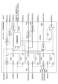
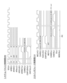
- the memory circuit 100 includes a memory block MBLK, a memory control section 200 (input side) connected to the input side of the memory block MBLK, and a memory control section 200 (output side) connected to the output side of the memory block MBLK.
- the memory control unit 200 (input side) is an example of a first memory control unit
- the memory control unit 200 (output side) is an example of a second memory control unit.
- the memory control unit 200 (input side) and 200 (output side) will be referred to as the memory control unit 200 when described without distinction.
- the memory block MBLK has a plurality of memory groups MG including a plurality of memory cells and arranged in one direction, and a plurality of memory group control units MCNT arranged on the signal input side of each of the plurality of memory groups MG. .
- the memory block MBLK also has a memory group control unit MCNT arranged on the signal output side of the memory group MG at the final stage.
- each memory group MG is arranged between a pair of memory group controllers MCNT.
- the memory group control units MCNT and the memory groups MG are alternately arranged.
- the memory group control unit MCNT functions as an interface circuit for signals input/output between the memory control unit 200 and the memory group MG, or as an interface circuit for signals input/output between the memory group control units MCNT.
- Each memory group control unit MCNT has a flip-flop FF that receives access request signals (control signal CMD, address signal A, etc.), memory write data signal D, and read data signal Q, respectively.
- each memory group control unit MCNT receives an access request signal for a memory group MG adjacent to its output side (hereinafter also referred to as its own memory group MG or managed memory group MG)
- each memory group control unit MCNT outputs an access request signal to its own memory group. Output to MG.
- the memory group control unit MCNT that outputs an access request signal to the memory group control unit MCNT of interest is referred to as the preceding memory group control unit MCNT.
- a memory group control unit MCNT that receives an access request signal from the memory group control unit MCNT of interest is referred to as a subsequent memory group control unit MCNT.
- each memory group control unit MCNT suppresses the output of the access request signal to the memory group control unit MCNT at the subsequent stage, except for the signal used by the memory group control unit MCNT at the final stage.
- the memory group control unit MCNT in the subsequent stage is the memory group control unit MCNT located on the memory control unit 200 (output side) side with one memory group MG in between with respect to the memory group control unit MCNT of interest.
- each memory group control unit MCNT when each memory group control unit MCNT receives an access request signal for a memory group MG other than its own memory group MG, it transfers the access request signal to the subsequent memory group control unit MCNT. In this case, each memory group control unit MCNT suppresses the output of the access request signal to its own memory group MG.
- Each memory group control unit MCNT transmits a memory read data signal Q read from its own memory group MG during a read operation or a memory read data signal Q transferred from the preceding memory group control unit MCNT to the subsequent memory group control unit MCNT. Forward.
- each memory group control unit MCNT Since the command line CMD, address line A, write data line D, and read data line Q are not wired over a long distance across a plurality of memory groups MG, an increase in wiring load can be suppressed. As a result, an increase in power consumption can be suppressed while suppressing an increase in the access time of the memory circuit 100 .
- the number of clock cycles required for transferring the access request signal, the memory write data signal D and the memory read data signal Q between the pair of memory group control units MCNT arranged on both sides of the memory group MG is set to be the same. be done. For example, the number of clock cycles required for signal transfer between a pair of memory group control units MCNT arranged on both sides of the memory group MG is "1". Signals transferred between the memory group control units MCNT are not affected by the load (signal skew, etc.) of the signal wiring in the memory group MG. can always be the same.
- the number of clock cycles should be increased according to the number of additions.
- timing design can be easily performed even when the number of memory groups MG is increased or decreased to newly design another memory circuit having a different storage capacity.
- the memory group control unit MCNT at the final stage adjacent to the memory control unit 200 (output side) does not have the memory group MG to be managed, but has the function of re-taking the timing for the memory control unit 200 (output side). have.
- the final-stage memory group controller MCNT that does not have a managed memory group MG is functionally a subset of the other memory group controllers MCNT.
- the memory control unit 200 is connected to a system bus SBUS of the semiconductor device and peripheral buses for inputting/outputting various control signals CNTL.
- the system bus SBUS may input/output signals based on AXI4 (Advanced eXtensible Interface 4) (trademark of another company) of ARM Corporation (trademark of another company), for example.
- the memory control unit 200 functions as an interface circuit between signals input/output to/from the system bus SBUS and signals input/output to/from the memory group control unit MCNT.
- FIG. 1 shows an example in which two columns of memory group control units MCNT and memory groups MG are arranged between the memory control unit 200 (input side) and the memory control unit 200 (output side).
- the number of columns of the memory group control units MCNT and the memory groups MG should be one or more.
- the columns of the memory group control units MCNT and the memory groups MG may be arranged in a U shape.
- the memory control unit 200 (input side) and the memory control unit 200 (output side) are collectively arranged on one end side of the arrangement area of the memory group control unit MCNT and the memory group MG.
- the memory control unit 200 transmits a request signal REQ for a read operation or a write operation to the memory circuit 100, an address signal ADR, a write data signal WD, etc. to a CPU (Central Processing Unit) or the like via the system bus SBUS. Received from the upper controller.
- the request signal REQ is an example of a request signal (access request signal) that causes the memory group MG to perform a write operation or a read operation, or a request signal that causes the memory group MG to change the operation mode.
- the access request signal is a write request signal or a read request signal. Note that FIG. 1 shows only the main flow of information signals for the sake of simplification of the drawing. Although not shown, there are also additional information, signals indicating whether each signal is valid or invalid, or control signals indicating data output instructions, data capture instructions, and the like.
- the memory control unit 200 (input side) outputs the control signal CMD including additional information for accessing the memory in the memory group MG based on the request signal REQ including information such as the address signal ADR, request ID or access size. Generate.
- the memory control unit 200 (input side) outputs the generated control signal CMD to the first-stage memory group control unit MCNT.
- the memory control unit 200 outputs the 512-bit memory write data signal D by 256 bits to the first two memory group control units. Output to MCNT. That is, the memory control unit 200 (input side) converts the N-bit (64 bits in this example) write data signal WD received from the system bus SBUS into (N ⁇ M) bits (M is "8" in this example). , and causes the memory group MG to execute the write operation of the memory write data signal D.
- all 512 bits of the memory write data signal D may not be valid data. Only valid data is written to the memory circuit 100 by the mask information.
- the memory control unit 200 (input side) also receives a control signal CNTL that sets the operation specifications of at least one of the memory group MG and the memory group control unit MCNT via the peripheral bus. Furthermore, the memory control unit 200 (input side) outputs the operation specification of at least one of the memory group MG and the memory group control unit MCNT to the peripheral bus as a control signal CNTL.
- the peripheral bus is a slower interface than the system bus SBUS.
- the memory control unit 200 receives access control signals such as the command signal CMD and the address signal A from one of the last-stage two memory group control units MCNT.
- the memory control unit 200 receives the memory read data signal Q from the last-stage two memory group control units MCNT, and outputs the read data signal RDT to the system bus SBUS.
- the memory control unit 200 outputs the 64-bit read data signal RDT eight times each time it receives two 256-bit memory read data signals Q.
- the 512-bit data input/output to/from the memory block BLK is eight times the 64-bit data input/output to/from the system bus SBUS. Therefore, ideally, the operating frequency of the memory block MBLK can be reduced to 1/8 of the operating frequency of the system bus SBUS. Therefore, power consumption of the memory block MBLK can be reduced as compared with the case of inputting/outputting 64-bit data to/from the memory block MBLK. Since the operating frequency of the memory block MBLK can be lowered, the operating margin of the memory group control unit MCNT and the memory group MG can be increased, and the timing design of the circuit can be easily performed.
- FIG. 2 is a block diagram showing an example of the memory control unit 200 of FIG.
- the memory control unit 200 (input side) has a system bus input control unit 202 , buffers 204 and 206 , a peripheral bus control unit 208 , an overall control unit 210 , a memory state control unit 212 and an input interface control unit 214 .
- the memory controller 200 (output side) has an output interface controller 220 , buffers 222 and 224 and a system bus output controller 226 .
- a system bus input control unit 202 buffers a command signal CMD containing additional information for memory control and an address signal A from an address signal ADR received from the system bus SBUS, a request signal REQ containing information such as a request ID or an access size. 204, and the write data signal WD received from the system bus SBUS is received eight times at maximum, resulting in 512-bit data and 1-bit additional information (Last information), for a total of 513 bits (hereinafter, the description of the Last signal will be 512 bits in total) are stored in the buffer 206 .
- the buffers 204 and 206 are, for example, FIFO (First-In First-Out) buffers.
- Buffer 204 outputs control signal CMD and address signal A to input interface control section 214 in the order in which they are held.
- the buffer 206 outputs the write data WD to the input interface control unit 214 in the order in which they are held.
- the buffer 204 outputs 512-bit memory write data WD to the input interface controller 214 .
- the input interface control unit 214 waits for valid information to be prepared in the buffer 204 .
- the information in the buffer 204 becomes valid, the information A is checked, and if the state of the memory area to be accessed in the target memory block MBLK is not in the active state, processing is performed to make it active.
- the active state the CMD information in the buffer 204 is checked, and in the case of a read operation for the memory block MBLK, the information in the buffer 204 is taken out, and the control signal CMD and the address A etc. for executing the read operation to the memory block MBLK are sent. Output to memory block MBLK.
- the peripheral bus control unit 208 outputs various control signals CNTL received from the peripheral bus to the overall management unit 210 . In addition, the peripheral bus control unit 208 outputs various control signals CNTL received from the overall management unit 210 to the peripheral bus.
- the overall management unit 210 has a plurality of registers (not shown) for setting operation specifications such as the operation mode of the memory group MG (FIG. 1).
- the general manager 210 sets registers according to various control signals CNTL from the peripheral bus.
- operating modes include shutdown mode, sleep mode, and active mode.
- the shutdown mode, sleep mode, and active mode are switched for each memory unit column MUC, which will be described later. Note that the units for switching between the shutdown mode, the sleep mode, and the active mode are not limited to the memory unit column MUC.
- the shutdown mode in the memory unit column MUC to be shut down, power to the memory cell area is cut off, and power to peripheral circuits not related to shutdown and sleep control is cut off for peripheral circuits other than the memory cell area.
- the sleep mode in the sleep-targeted memory unit column MUC, the power supply of the memory cell area is lowered to a low voltage that can maintain the data held in the memory cells, and the peripheral circuits other than the memory cell area are shut down and put into sleep mode. Power to peripheral circuits not related to control is cut off.
- the memory block MBLK itself has a built-in power supply circuit for the shutdown function and the sleep function.
- the power supply voltage of the memory cell area can be adjusted, and the power supply voltage of the peripheral circuits other than the memory cell area can be adjusted or the power supply can be cut off. If so, this technique is applicable.
- the register of the memory state management unit 212 may be set with a period of time until transition to the sleep mode when there is no access during the active mode.
- the memory state management unit 212 manages the operation mode of the memory unit array MUC based on the set values of the multiple internal registers. In addition, the memory state management unit 212 holds defect information indicating the position of a defective memory cell in the memory group MG, and manages access to a normal memory cell instead of the defective memory cell.
- the output interface control unit 220 stores two 256-bit memory read data signals Q received from the memory block in the buffer 224 in the read operation of the memory block MBLK. Output interface control unit 220 also stores control signal CMD including additional information for memory control and address signal A received from memory block MBLK in buffer 222 .
- Buffers 222 and 224 are, for example, FIFO buffers.
- Buffer 222 outputs control signal CMD including additional information for memory control and address signal A to system bus output control section 226 in the order in which they are held.
- the buffer 224 outputs the two 256-bit memory read data signals Q to the system bus output controller 226 as 512-bit read data.
- the memory control unit 200 has a function of mutually converting the frequency of data input/output to/from the system bus SBUS and the frequency of data input/output to/from the memory block MBLK.
- the input sides of the buffers 204 and 206 operate with the system clock signal SCLK used by the system bus SBUS.
- the output sides of the buffers 204 and 206 operate with the memory clock signal MCLK used in the memory block MBLK.
- the input sides of the buffers 222 and 224 operate with the memory clock signal MCLK used in the memory block MBLK.
- the output sides of the buffers 222 and 224 operate with the system clock signal SCLK used by the system bus SBUS. In this manner, buffers 204, 206, 222, 224 also operate as clock domain crossing circuits.
- the system bus output control unit 226 receives the control signal CMD including additional information for memory control output from the buffer 222 and the address signal A, and the 512-bit memory read data signal Q output from the buffer 224. .
- the system bus output control unit 226 converts the 512-bit memory read data signal Q into a maximum of eight 64-bit read data RDT according to the control signal CMD including additional information for memory control and the address signal A. They are sequentially output to the bus SBUS.
- the 512-bit memory read data signal Q may include data that is not to be accessed. Only data to be accessed is output to the system bus SBUS.
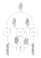
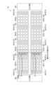
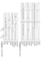
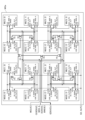
- FIG. 3 shows an example of the configuration of the memory block MBLK in FIG.
- memory block MBLK is described as having eight memory groups MG (MG10, MG11, MG20, MG21, MG30, MG31, MG40, MG41), two vertically and four horizontally.
- the number and arrangement of memory groups MG mounted in memory block MBLK are not limited to the example shown in FIG.
- the memory block MBLK has memory group control units MCNT (MCNT10, MCNT11, MCNT20, MCNT21, MCNT30, MCNT31, MCNT40, MCNT41) arranged on the input side of each memory group MG.
- the memory block MBLK also has memory group control units MCNT50 and MCNT51 arranged on the output sides of the final-stage memory groups MG40 and MG41, respectively.
- Each memory group MG has 16 memory units MU, 4 vertically and 4 horizontally.
- the number and arrangement of memory units MU mounted in each memory group MG are not limited to the example shown in FIG.
- a memory group column MGC is formed by two memory groups MG arranged in the vertical direction.
- a memory unit column MUC is formed by four memory units MU arranged in the vertical direction.
- Memory unit column MUC is an example of a sub memory group.
- each memory group column MGC is identified by bits AD[24:23] of the address signal A of 25 bits.
- Each memory unit column MUC is identified by bits AD[22:21] of address signal A of 25 bits.
- the unit for switching between shutdown mode, sleep mode, and active mode is the memory unit column MUC.
- Sleep mode is an example of a low power mode.
- the memory unit column MUC is an example of a sub memory group that is a unit for switching between sleep mode and active mode.
- the shutdown mode, sleep mode, and active mode may be switched in units of two vertical memory unit columns MUC, or may be switched in units of columns obtained by subdividing the memory unit column MUC into a plurality of columns. For example, the switching may be performed in units of memory columns MEMC in FIG. 5, which will be described later. Furthermore, the shutdown mode, sleep mode, and active mode may be switched for each memory group MG.
- the power consumption in shutdown mode is about 1/10 of the standby power in active mode, and the power consumption in sleep mode is 3/3 of the standby power in active mode. It is about 1.
- the memory group control unit MCNT on the input side of each memory group MG sends a control signal CMD, an address signal A and a memory write data signal D to the memory group MG and the memory group control unit MCNT on the output side of the memory group MG. Output.
- Each memory group MG outputs a memory read data signal Q to the memory group control unit MCNT on the output side.
- command lines CMD and address lines A are not routed across a plurality of memory groups MG. Therefore, an increase in wiring load can be suppressed. As a result, an increase in power consumption can be suppressed while suppressing an increase in the access time of the memory circuit 100 .
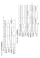
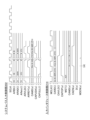
- FIG. 4 shows an example of the configuration of the memory group MG in FIG.
- a symbol (i) attached to the end of a signal indicates an input signal, and a symbol (o) attached to the end of a signal indicates an output signal.
- the memory group MG receives the memory clock signal MCLK, 16 chip enable signals CEB, write enable signal WEB and bit write enable signal BWEB from the memory group controller MCNT as the control signal CMD in FIG.
- the 16 chip enable signals CEB are supplied four by four to the memory unit column MUC and used to select the memory unit column MUC and the memory column MEMC (FIG. 5, which will be described later) within the memory unit column MUC.
- a signal with a sign B at the end is a signal of negative logic
- a signal without a sign B at the end is a signal of positive logic
- the bit write enable signal BWEB is a signal that controls the writing of data signals in units of bits, and the bit write enable signal BWEB corresponding to the bit whose writing is masked is set to high level.
- the memory group MG receives an address signal A and a 256-bit memory write data signal D, and outputs a memory read data signal Q.
- the 256-bit memory write data signal D is supplied to four memory units MU of the memory unit column MUC by 64 bits.
- the memory group MG has a plurality of selectors SEL that select one of the 64-bit memory read data signals Q output from the four memory units MU arranged in the horizontal direction and output it to the memory group control unit MCNT.
- the memory group MG receives the shutdown signal SD and the sleep signal SLP from the memory group controller MCNT as the control signal CMD in FIG. As described with reference to FIG. 3, in this embodiment, switching between shutdown mode, sleep mode, and active mode is performed for each memory unit column MUC. Therefore, the shutdown signal SD and sleep signal SLP are supplied for each memory unit column MUC.
- a symbol SDO of each memory unit MU indicates a terminal that outputs a shutdown signal SD to adjacent memory units MU in the memory unit column MUC.
- a symbol SLPO of each memory unit MU indicates a terminal for outputting a sleep signal SLP to an adjacent memory unit MU in the memory unit column MUC.
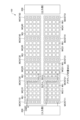
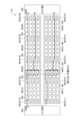
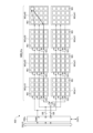
- FIG. 5 shows an example of the configuration of the memory unit MU in FIG.
- the memory unit MU has eight memories MEM, two vertically and four horizontally.
- the memory MEM has a plurality of SRAM memory cells, but may have other volatile memory cells.
- the memory MEM may also have memory cells of non-volatile memory such as MRAM (Magnetoresistive Random Access Memory) or ReRAM (Resistive Random Access Memory). Note that the number and arrangement of the memories MEM mounted in the memory unit MU are not limited to the example shown in FIG.
- the memory MEM in the memory unit MU sequentially transmits the shutdown signal SD and the sleep signal SLP in the same way as the memory unit MU in the memory group MG shown in FIG. Thereby, the peak current can be further suppressed.
- the shutdown signal SD and the sleep signal SLP may be further subdivided.
- the peak current can be further suppressed by controlling the shutdown signal SD and the sleep signal SLP for each memory column MEMC including two memories MEM arranged in the vertical direction.
- FIG. 6 shows an example of read and write operations of the memory MEM of FIG.
- shutdown signal SD and sleep signal SLP must be fixed at low level (L)
- memory unit column MUC to be operated must be in an active state.
- a read operation is started at the rising edge of the clock signal CLK when the chip enable signal CEB is at low level and the write enable signal WEB is at high level.
- the memory MEM reads data from the memory area indicated by the address signal A received in synchronization with the rising edge of the clock signal CLK, and outputs the memory read data signal Q after the time tcd from the rising edge of the clock signal CLK.
- a write operation is started at the rising edge of the clock signal CLK when the chip enable signal CEB is at low level and the write enable signal WEB is at low level.
- the memory MEM receives the address signal A and the memory write data signal D in synchronization with the rising edge of the clock signal CLK. Then, the memory MEM writes the memory write data signal D to the memory area indicated by the received address signal A. FIG. However, the memory MEM masks the write operation for the bit value of the bit write enable signal BWEB received in synchronization with the rising edge of the clock signal MCLK and having a high level bit.
- FIG. 6 shows that in Write Cycle i, since the BWEB(i) bit is low level, the value of the corresponding D(i) bit is written to the memory cell, and since the BWEB(j) bit is high level, the corresponding D(j ) writes of bit values to memory cells are masked. Also, in Write Cycle j, since the BWEB(j) bit is at low level, the corresponding D(j) bit is written to the memory cell, and since the BWEB(i) bit is at high level, the corresponding D(i) bit is written to the memory cell. Writes to the cell are masked. Although not shown in the figure, when all BWEB bits are at low level, the values of all D bits are written to memory cells, and when all BWEB bits are at high level, all D bits are written to memory cells. Writing values to memory cells is masked.
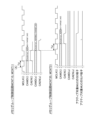
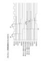
- FIG. 7 shows an example of the configuration of the memory group control unit MCNT of FIG.
- the memory group controller MCNT has a plurality of flip-flops FF (FF1, FF2, FF3, FF4, FF5, FF6, FF7), a relay controller RCNT, and a plurality of mask circuits MSK (MSKC, MSKW1, MSKW2, MSKR).
- a plurality of flip-flops FF are connected to the thick signal line.
- a signal suffixed with (i) indicates an input signal
- a signal suffixed with (o) indicates an output signal.
- PARAM(i) is a multi-bit signal used to identify the memory group control unit MCNT, and is fixed to high level or low level bit by bit.
- the logic of the PARAM(i) signal is determined when memory circuit 100 is designed.
- Reference CAWD(i) indicates the control signal CMD and the address A received from the preceding memory group control unit MCNT.
- Symbol D[255:0](i) indicates the memory write data signal D received from the preceding memory group controller MCNT.
- the upper code Q[255:0](i) indicates the memory read data signal Q from the preceding memory group MG.
- the lower code Q[255:0](i) indicates the memory read data signal Q received from the preceding memory group control unit MCNT.
- a symbol CAWD(o) indicates the control signal CMD and the address signal A to be output to the subsequent memory group control unit MCNT.
- Symbols CEB[3:0], WEB[3:0], A, BWEB, SLP[3:0], and SD[3:0] indicate various control signals and address signal A output to its own memory group MG.
- the upper code D[255:0](o) indicates the memory write data signal D output to the memory group control unit MCNT in the subsequent stage.
- the lower code D[255:0](o) indicates the write data signal D output to its own memory group MG.
- Reference character Q[255:0](o) indicates a memory read data signal Q to be output to the memory group control unit MCNT in the subsequent stage.
- the memory clock signal MCLK is transmitted to each synchronization circuit in the memory group control unit MCNT via the buffer BUF1.
- the memory clock signal MCLK output from the buffer BUF1 is output to the subsequent memory group control unit MCNT via the buffer BUF2.
- the memory clock signal MCLK output from the buffer BUF1 is output to its own memory group MG as the memory clock signal IMCLK via the buffer BUF3.
- command address enable signal CAEN When the command address enable signal CAEN is at the valid level, the flip-flop FF1 holds and outputs the received control signal CMD, address signal A, and additional information (command address signal CAWD).
- Command address enable signal CAEN is output from memory control unit 200 together with control signal CMD and address signal A.
- FIG. The flip-flop FF2 transfers the command address enable signal CAEN received from the memory control unit 200 or the preceding memory group control unit MCNT to the succeeding memory group control unit MCNT. For example, the valid level of the command address enable signal CAEN is high level.
- the flip-flop FF3 holds and outputs the received 256-bit write data signal D when the write data enable signal WDEN is at the valid level.
- the write data enable signal WDEN is output from the memory control section 200 together with the write data signal D.
- FIG. The flip-flop FF4 transfers the write data enable signal WDEN received from the memory controller 200 or the preceding memory group controller MCNT to the subsequent memory group controller MCNT. For example, the valid level of the write data enable signal WDEN is high level.
- the flip-flop FF5 holds and outputs the 256-bit memory read data signal Q received via the selector SELQ when the read data enable signal RDEN received from the preceding memory group control unit MCNT is at a valid level.
- the valid level of the read data enable signal RDEN is high level.
- the memory read data signal Q is output from the preceding memory group MG and the preceding memory group control unit MCNT.
- the preceding memory group MG is a memory group MG arranged adjacent to the memory control unit 200 (input side) with respect to the memory group control unit MCNT of interest.
- the operation of the preceding memory group MG is controlled by the preceding memory group control unit MCNT of the focused memory group control unit MCNT.
- the selector SELQ selects the memory read data signal Q read from the preceding memory group MG or the memory read data signal Q transferred from the preceding memory group control unit MCNT, according to the level of the control signal from the relay control unit RCNT. do.
- the memory read data signal Q can be transferred to the memory control unit 200 by the selector SELQ regardless of the position of the memory group MG that outputs the memory read data signal Q.
- the read data enable signal RDEN is output from either the preceding stage or the memory group control section MCNT preceding the preceding stage.
- the flip-flop FF6 transfers the read data enable signal RDEN received from the preceding memory group control unit MCNT to the succeeding memory group control unit MCNT via the OR circuit OR.
- the first stage memory group control unit MCNT does not receive the memory read data signal Q from the preceding stage memory group MG and the memory read data signal Q from the preceding stage memory group control unit MCNT.
- the memory group control unit MCNT in the second stage does not receive the memory read data signal Q from the memory group control unit MCNT in the previous stage.
- the flip-flop FF7 in the memory group control unit MCNT in the previous stage receives the read data enable signal IRDEN output from the relay control unit RCNT, and receives the read data enable signal IRDEN output from the relay control unit RCNT. Output to the memory group control unit MCNT of interest.
- the memory read data signal Q in which data is read from the memory group MG in the previous stage is taken in by the flip-flop FF5 in the memory group control unit MCNT in the subsequent stage.
- the valid level of the read data enable signal IRDEN is high level.
- the relay control unit RCNT controls the operation of the relay control unit RCNT itself and also controls the operation of the memory group MG in the subsequent stage.
- the memory group MG in the subsequent stage is a memory group MG arranged adjacent to the memory control unit 200 (output side) with respect to the memory group control unit MCNT of interest, and is operated by the memory group control unit MCNT of interest.
- a controlled memory group MG is a memory group MG arranged adjacent to the memory control unit 200 (output side) with respect to the memory group control unit MCNT of interest, and is operated by the memory group control unit MCNT of interest.
- the relay control unit RCNT operates according to a parameter signal PARAM for indicating at what stage from the memory control unit 200 the memory group control unit MCNT is.
- Each bit of the parameter signal PARAM is fixed to a high level or a low level outside each memory group control unit MCNT based on the overall design of the memory circuit 100, and each memory group control unit MCNT determines which stage memory Specifies whether it is a group control unit MCNT. For example, in the configuration of FIG. 3, there are five memory group control units MCNT in the horizontal direction. In this case, the PARAM signal indicates any one of 0 to 7 with 3 bits.
- the relay control unit RCNT can detect the memory group MG executing the write operation or the read operation.
- the relay control unit RCNT outputs a low-level chip enable signal CEB, a low-level write enable signal WEB, an address A, and a bit write enable signal BWEB to the subsequent memory group MG when determining the write operation of the subsequent memory group MG.
- Chip enable signal CEB and write enable signal WEB are generated corresponding to each of four memory unit columns MUC in memory group MG in the subsequent stage.
- the relay control unit RCNT determines the read operation of its own memory group MG, it outputs a low-level chip enable signal CEB, a high-level write enable signal WEB, and an address A to the read target memory unit column MUC.
- the relay control unit RCNT When determining that the memory group MG is to be switched to the sleep mode or the shutdown mode, the relay control unit RCNT outputs a sleep signal SLP and a shutdown signal SD at a predetermined logic level to the memory unit column MUC to be controlled. Sleep signal SLP and shutdown signal SD are generated corresponding to each of four memory unit columns MUC within own memory group MG.
- the relay control unit RCNT outputs a low-level sleep signal SLP and a low-level shutdown signal SD to its own memory group MG when it determines that the sleep mode or shutdown mode of its own memory group MG is to be released.
- the state of each memory unit column MUC is collectively managed by the memory state management section 212 in the memory control section 200 . Then, if the sleep mode or shutdown mode needs to be released before the write operation or read operation is executed, the memory control unit 200 outputs the command for the write operation or read operation before the memory unit MUC. Output change commands that change state.
- the sleep signal SLP and shutdown signal SD are set to low level and high level, respectively.
- sleep signal SLP and shutdown signal SD are set to high and low levels, respectively.
- sleep signal SLP and shutdown signal SD are both set to low level.
- the sleep signal SLP and the shutdown signal SD are set to low level and high level, respectively, and the memory unit columns MUC in all memory groups MG are set to the shutdown mode. After that, only the memory unit column MUC to be operated is shifted from the shutdown mode to the active mode ACT, and the write operation or read operation is performed. Further, when there is no access for a predetermined period during the active mode, the memory control unit 200 outputs a command to change the memory state, and the memory unit column MUC in the memory group MG managed by the corresponding memory group control unit MCNT is Transition from active mode to sleep mode.
- the predetermined period for judging the transition from the active mode to the sleep mode can be changed by setting the register value of the memory state management unit 212 in FIG.
- the memory unit column MUC in sleep mode or active mode can shift to shutdown mode based on an instruction from the memory control section 200 .
- the memory unit column MUC in which the write operation or read operation is performed is set to the active mode, and the active mode is maintained while the access is continuously performed. Also, if there is no access for a certain period of time, it is returned to sleep mode.
- power consumption of the memory circuit MEM can be reduced.
- the relay control unit RCNT Based on the control signal CMD and the address signal A received from the preceding memory group control unit MCNT, the relay control unit RCNT detects that the memory read data signal Q is output from the preceding stage or the preceding stage memory group MG. . When the memory read data signal Q is output from the preceding memory group MG, the relay control unit RCNT selects the memory read data signal Q from the preceding memory group MG with the selector SELQ. When the memory read data signal Q is output from the memory group MG preceding the previous stage, the relay control unit RCNT selects the memory read data signal Q transferred from the memory group control unit MCNT of the preceding stage with the selector SELQ.
- the relay control unit RCNT releases the masking state of the mask circuit MSKR when the read data enable signal RDEN is at a valid level (for example, high level), and closes the mask circuit MSKR when the read data enable signal RDEN is at an invalid level (for example, low level). to be masked.
- the memory group control unit MCNT receives the 256-bit memory read data signal Q by executing the read operation of the memory group MG in the preceding stage, the memory group control unit MCNT relays the memory read data signal Q to the memory group control unit MCNT in the subsequent stage.
- the relay control unit RCNT when the relay control unit RCNT does not receive the memory read data signal Q from the previous stage, it suppresses the transfer of the invalid memory read data signal Q to the memory group control unit MCNT in the subsequent stage. Thereby, power consumption can be reduced.
- the relay control unit RCNT outputs a memory read data signal Q from its own memory group MG based on the control signal CMD, the address signal A, and the command address signal CAWD including additional information received from the preceding memory group control unit MCNT. detect that When the memory read data signal Q is output from its own memory group MG, the relay control unit RCNT outputs the read data enable signal IRDEN of a valid level to the flip-flop FF7. The flip-flop FF7 outputs the read data enable signal IRDEN to the subsequent memory group control unit MCNT via the OR circuit OR.
- the relay control unit RCNT outputs the read data enable signal IRDEN in the same cycle as the chip enable signal CEB for causing the subsequent memory group MG to perform the read operation. Therefore, the read data enable signal RDEN output from the flip-flop FF7 is supplied to the subsequent memory group control unit MCNT one cycle after the read operation of the subsequent memory group MG is started. Therefore, the subsequent memory group control unit MCNT can hold the memory read data signal Q received from the corresponding memory group MG in the flip-flop FF5.
- the relay control unit RCNT cancels the masking state of the mask circuit MSKR in order to transfer the memory read data signal Q to the memory group control unit MCNT in the subsequent stage when the read operation is performed in the memory group MG in the preceding stage or in the preceding stage. do. Further, when the write operation is performed in the memory group MG in the subsequent stage or in the subsequent stage, the relay control unit RCNT releases the masking state of the mask circuit MSKW1 in order to transfer the write data signal D to the subsequent stage MCNT. In addition, the mask circuit MSKW2 is set to the mask state in order to suppress the transfer of the write data signal D to its own memory group MG.
- the relay control unit RCNT sets the mask state of the mask circuit MSKC to be released in order to transfer the control signal CMD, the address signal A, and the command address signal CAWD including the additional information to the subsequent memory group control unit MCNT.
- the relay control unit RCNT transfers the control signal CMD, the address signal A, and the command address signal CAWD including additional information to the memory group control unit MCNT in the subsequent stage when the write operation is performed in the memory group MG in the subsequent stage or in the subsequent stage. In order to do so, the mask state of the mask circuit MSKC is released.
- the relay control unit RCNT sets the mask circuit MSKC to the mask state in order to transfer the command address signal CAWD to the subsequent memory group control unit MCNT.
- the final-stage memory group control unit MCNT can perform control to output the control signal CMD, the address signal A, the command address signal CAWD including additional information, and the memory read data signal Q to the memory control unit 200. can.
- the relay control unit RCNT sets the mask circuit MSKW1 to a masked state in order to suppress transfer of the write data signal D to the subsequent memory group control unit MCNT. Furthermore, in order to transfer the memory write data signal D to its own memory group MG, the masking state of the mask circuit MSKW2 is released.
- the relay control unit RCNT cancels the masking state of the mask circuit MSKW1 in order to transfer the write data signal D to the memory group control unit MCNT in the subsequent stage when the write operation is performed in the memory group MG in the subsequent stage and in the subsequent stage.
- the relay control unit RCNT sets the mask circuit MSKW2 to a masked state in order to suppress the transfer of the memory write data signal D to its own memory group MG when the write operation is performed in the memory group MG in the subsequent stage and in the memory group MG subsequent to the subsequent stage. do.
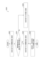
- FIG. 8 shows an example of transition of the operating state of the memory unit column MUC of FIG.
- the state transitions in FIG. 8 are managed by the memory group controller MCNT that controls the operation of the memory unit array MUC.
- transition to the shutdown mode SD is performed by register setting of the memory state management unit 212 of the memory control unit 200 .
- FIG. 8 shows state transitions in units of switching among shutdown mode SD, sleep mode SLP, and active mode ACT. Therefore, when the unit of switching between the shutdown mode SD, the sleep mode SLP, and the active mode ACT is the memory group MG, FIG. 8 shows the state transition of the memory group MG. When the operation mode is switched in units of memory columns MEMC in the memory unit column MUC, FIG. 8 shows state transitions in units of memory columns MEMC. An example of control for each memory unit column MUC will be described below.
- the state of all the memory unit columns MUC is set to the shutdown mode SD.
- a memory unit column MUC in which a write request or a read request has occurred is transitioned from the shutdown mode SD to the active transition mode ATRNS, and, for example, peripheral circuits other than the memory cell area are powered on.
- the memory unit column MUC transitions to the active mode ACT after the elapse of time for the power supply to be stabilized, and the write operation or read operation is performed.
- active mode ACT a write operation or read operation is executed each time a write request or read request for the memory unit column MUC is generated.
- the memory unit column MUC In the active mode ACT, if a non-access state in which no write request or read request is generated continues for a predetermined time, the memory unit column MUC is transitioned to the sleep mode SLP.
- the sleep mode SLP is an example of a low power mode that suppresses power consumption while holding data held by the memory unit column MUC.
- the power consumption of the memory circuit 100 can be reduced by switching the memory unit column MUC, which does not perform the write operation or the read operation for a predetermined period, from the active mode ACT to the sleep mode SLP.
- the memory unit column MUC for which a write request or read request has occurred is transitioned to the active transition mode ATRNS.
- the memory unit column MUC is shifted to the shutdown mode SD when a shutdown instruction for the memory unit column MUC is issued in the active mode ACT or the sleep mode SLP.
- the shutdown instruction is performed by register setting of the memory state management unit 212 based on reception of the control signal CTNL in FIG. 2, for example.
- the memory unit row MUC transitions to the shutdown mode SD when the sleep mode SLP continues for a predetermined time.
- the duration of the sleep mode SLP may be preset in the register of the general manager 210 of FIG.
- the automatic transition to the shutdown mode SD is performed, for example, when the frame image data held in the memory circuit 100 is always accessed within a certain period of time during processing of a moving image, and if there is no access for the certain period of time or longer, there is an automatic transition to the shutdown mode SD.
- This is the case, for example, when it can be guaranteed that the data held in the For example, when memory access processing is being performed on a certain screen size, it is used when processing on the first screen size, such as when switching to a smaller screen size and memory access processing continues.
- When switching to a smaller screen size in the memory area unused memory area occurs.
- access control of the memory circuit 100 can be facilitated compared to issuing a shutdown instruction from the outside. can be done.
- the duration of the sleep mode SLP until transition to the shutdown mode SD may be set based on the acquired statistical information obtained by obtaining statistical information such as access frequency.
- the memory control unit 200 acquires statistical information such as the time from the transition to the sleep state to the active state, the frequency of transition from the active state to the sleep state, and the frequency of access in the active state. A circuit and a duration calculation circuit are added.
- FIGS. 9 to 13 show an example of the operation of the memory group control unit MCNT shown in FIG.
- the processes shown in FIGS. 9 to 13 are executed for each memory unit column MUC by the relay control units RCNT of the plurality of memory group control units MCNT in the memory circuit 100.
- FIG. Note that the processing shown in FIGS. 9 to 13 shows an example in which the unit of switching among the shutdown mode SD, the sleep mode SLP, and the active mode ACT is the memory unit column MUC.
- step S10 the relay control unit RCNT waits until it detects a positive edge of the system clock signal SCLK, and when it detects a positive edge, it executes step S12.
- step S12 the relay control unit RCNT executes step S100 (state transition processing) when a state transition request is issued, and executes step S14 when a state transition request is not issued.
- step S100 state transition processing
- the state transition request is an active command for transitioning to active mode ACT, a sleep command for transitioning to sleep mode SLP, or a shutdown command for transitioning to shutdown mode SD.
- the active command is issued by the corresponding relay control unit RCNT based on the issuance of a write request or read request.
- a shutdown command is issued by the memory control unit 200 based on a request issued to the memory circuit 100 via the system bus SBUS.
- the sleep command is issued by the corresponding relay control unit RCNT when the memory unit column MUC in active mode ACT is to be transitioned to sleep mode SLP. Note that the sleep command may be issued by the memory control unit 200 based on a request issued to the memory circuit 100 via the system bus SBUS.
- step S14 the relay control unit RCNT executes step S200 (read operation) if a read request has been issued, and executes step S16 if no read request has been issued.
- step S200 is shown in FIGS.
- step S16 the relay control unit RCNT executes step S300 (write operation) if a write request has been issued, and returns to step S10 if a write request has not been issued.
- step S300 is shown in FIG.
- step S100 the relay control unit RCNT executes the state transition process shown in FIG. 10, and returns to step S10.
- step S200 the relay control unit RCNT executes the read processing shown in FIG. 11, and returns to step S10.
- step S300 the relay control unit RCNT executes write processing and returns to step S10.
- FIG. 10 shows an example of step S100 (state transition processing) in FIG.
- the relay control unit RCNT determines whether or not the address signal A received together with the state transition command indicates its own memory group MG.
- the own memory group MG is the own memory group MG of the memory group control unit MCNT in the example of FIG. 1, and is the memory group MG to be accessed for executing the write operation or the read operation.
- the relay control unit RCNT executes step S104 when the address signal A indicates its own memory group MG, and executes step S116 when the address signal A does not indicate its own memory group MG.
- step S104 the relay control unit RCNT executes step S106 if the state transition command is the active command or the wake-up command.
- the relay control unit RCNT executes step S108 when the state transition command is not the active command or the sleep release command.
- step S106 the relay control unit RCNT outputs a low-level sleep signal SLP and a low-level shutdown signal SD to the active target memory unit column MUC indicated by the address signal A. As a result, the active target memory unit column MUC transitions to the active mode ACT. After step S106, step S114 is executed.
- step S108 the relay control unit RCNT executes step S110 if the state transition command is the sleep command, and executes step S112 if the state transition command is not the sleep command.
- step S110 the relay control unit RCNT outputs a high-level (H) sleep signal SLP and a low-level shutdown signal SD to the active target memory unit column MUC indicated by the address signal A (target for transition to the active mode ACT). do. As a result, the active target memory unit column MUC transitions to the sleep mode SLP.
- step S114 is executed.
- step S112 the relay control unit RCNT outputs a low-level sleep signal SLP and a high-level shutdown signal SD to the active target memory unit column MUC indicated by the address signal A. As a result, the active target memory unit column MUC transitions to the shutdown mode SD.
- step S114 is executed.
- step S114 the relay control unit RCNT suppresses transfer of the control signal CMD and the address signal A to the subsequent memory group control unit MCNT by setting the mask circuit MSKC to the mask state, and performs the processing shown in FIG. finish.
- step S116 the relay control unit RCNT sets the mask circuit MSKC to the unmasked state, thereby permitting the transfer of the control signal CMD and the address signal A to the memory group control unit MCNT in the succeeding stage. Terminate the indicated process.
- FIG. 11 shows an example of step S200 (read operation) in FIG.
- the relay control unit RCNT determines whether or not the address signal A received together with the read request signal indicates its own memory group MG.
- the relay control unit RCNT executes step S204 when the address signal A indicates its own memory group MG, and executes step S210 when the address signal A does not indicate its own memory group MG.
- step S204 the relay control unit RCNT outputs a low-level chip enable signal CEB to the read target memory unit column MUC indicated by the address signal A.
- the relay control unit RCNT outputs a high-level chip enable signal CEB to the memory unit columns MUC that are not to be read.
- step S206 the relay control unit RCNT outputs a high-level write enable signal WEB and a high-level bit write enable signal BWEB to its own memory group MG.
- the relay control unit RCNT outputs the received address signal A together with the control signal CMD to its own memory group MG.
- step S208 the target relay control unit RCNT corresponding to the read target memory group MG outputs a high-level read enable signal RDEN.
- the target relay control unit RCNT causes the selector SELQ to select the invalid memory read data signal Q from the preceding memory group control unit MCNT.
- the relay control unit RCNT may cause the selector SELQ to select an invalid memory read data signal Q from the preceding memory group MG.
- step S210 the relay control unit RCNT outputs a high-level chip enable signal CEB, a high-level write enable signal WEB, and a high-level bit write enable signal BWEB to each memory unit column MUC.
- the relay control unit RCNT outputs a low-level address signal A to each memory unit column MUC. Power consumption can be reduced by not causing the logic level of the address signal A to transition.
- step S212 the relay control unit RCNT determines whether or not the address signal A received together with the read request signal indicates the memory group MG on the previous stage side (the previous stage or before the previous stage).
- the relay control unit RCNT executes step S214 when the address signal A indicates the preceding memory group MG, and executes step S216 when the address signal A does not indicate the preceding memory group MG.
- the relay control unit RCNT outputs a low-level read enable signal RDEN. Further, the relay control unit RCNT causes the selector SELQ to select the memory read data signal Q from the preceding memory group MG or the memory read data signal Q from the preceding memory group control unit MCNT. As a result, the memory read data signal Q read from any of the memory unit columns MUC of the memory group MG on the front stage side can be transferred to the rear stage. Note that the relay control unit RCNT receives the high-level read enable signal RDEN output from the previous-stage memory group control unit MCNT at the OR circuit OR, and transfers it to the subsequent-stage memory group control circuit MCNT. After step S214, step S220 is performed.
- the relay control unit RCNT outputs a low-level read enable signal RDEN. Further, the relay control unit RCNT causes the selector SELQ to select the invalid memory read data signal Q from the preceding memory group control unit MCNT. Note that the relay control unit RCNT may cause the selector SELQ to select an invalid memory read data signal Q from the preceding memory group MG. After step S216, step S220 is performed.
- the relay control unit RCNT sets the masking state of the masking circuits MSKC and MSKR, and ends the operation shown in FIG.
- FIG. 12 shows an example of step S220 in FIG.
- the relay control unit RCNT sets the mask circuit MSKC to the unmasked state, and permits transfer of the control signal CMD and the address signal A to the memory group control unit MCNT in the subsequent stage.
- step S224 the relay control unit RCNT determines whether or not the memory group MG on the preceding stage executes the read operation based on the address signal A received together with the read request signal.
- step S226 is executed. If the preceding memory group MG does not execute the read operation, step S228 is executed.
- step S226 the relay control unit RCNT sets the mask circuit MSKR to the unmasked state, and transmits the memory read data signal Q from the preceding memory group MG or the memory read data signal Q from the preceding memory group control unit MCNT to the subsequent stage. be transferable to After step S226, step S230 is performed.
- step S2208 the relay control unit RCNT sets the mask circuit MSKR to the mask state because the memory read data signal Q from the preceding memory group MG or the memory read data signal Q from the preceding memory group control unit MCNT is not transferred. do. Power consumption can be reduced by suppressing the transfer of the invalid memory read data signal Q.
- step S230 is performed.
- the relay control unit RCNT sets the mask circuits MSKW1 and MSKW2 to the mask state, and ends the operation of FIG. By suppressing the transfer of the invalid write data signal D and the invalid memory write data signal D, power consumption can be reduced.
- FIG. 13 shows an example of step S300 (write operation) in FIG.
- the relay control unit RCNT determines whether or not the address signal A received together with the write request signal indicates its own memory group MG.
- the relay control unit RCNT executes step S304 when the address signal A indicates its own memory group MG, and executes step S312 when the address signal A does not indicate its own memory group MG.
- step S304 the relay control unit RCNT outputs a low-level chip enable signal CEB and a low-level write enable signal WEB to the write target memory unit column MUC indicated by the address signal A.
- the relay control unit RCNT outputs a high-level chip enable signal CEB and a high-level write enable signal WEB to memory unit columns MUC that are not to be written.
- step S306 the relay control unit RCNT outputs the bit write enable signal BWEB included in the control signal CMD and the address signal A received together with the control signal CMD to its own memory group MG.
- step S308 the relay control unit RCNT outputs a low-level read enable signal RDEN.
- the relay control unit RCNT causes the selector SELQ to select the invalid memory read data signal Q from the preceding memory group control unit MCNT.
- the relay control unit RCNT may cause the selector SELQ to select an invalid memory read data signal Q from the preceding memory group MG.
- step S310 the relay control unit RCNT sets the mask circuits MSKC and MSKW1 to the masked state, sets the mask circuit MSKW2 to the unmasked state, and ends the operation of FIG.
- the mask circuit MSKC By setting the mask circuit MSKC to the mask state, the transfer of the control signal CMD and the address signal A to the subsequent stage, which is not related to the write operation, is suppressed, so power consumption can be reduced.
- the mask circuit MSKW1 to the mask state the transfer of the memory write data signal D to the subsequent stage is suppressed, so power consumption can be reduced.
- the mask circuit MSK2 By setting the mask circuit MSK2 to the unmasked state, the memory write data signal D can be transferred to the memory unit column MUC to be written.
- step S312 the relay control unit RCNT outputs a high-level chip enable signal CEB, a high-level write enable signal WEB, and a high-level bit write enable signal BWEB to each memory unit column MUC.
- the relay control unit RCNT outputs a low-level address signal A to each memory unit column MUC.
- step S314 the relay control unit RCNT outputs a low-level read enable signal RDEN.
- the relay control unit RCNT causes the selector SELQ to select the invalid memory read data signal Q from the preceding memory group control unit MCNT.
- the relay control unit RCNT may cause the selector SELQ to select an invalid memory read data signal Q from the preceding memory group MG.
- step S316 the relay control unit RCNT sets the masking state or unmasking state of the masking circuits MSKC, MSKR, MSKW1, and MSKW2.
- the relay control unit RCNT sets the mask circuit MSCR to a mask state.
- the relay control unit RCNT determines whether or not the memory group MG on the preceding stage executes the write operation.
- the relay control unit RCNT sets the mask circuits MSKC, MSKW1, and MSKW2 to the unmasked state when the preceding memory group MG executes the write operation.
- the relay control unit RCNT sets the mask circuits MSKC and MSKW1 to the unmasked state, and sets the mask circuit MSKW2 to the masked state. Then, the relay control unit RCNT ends the operation of FIG.
- power consumption can be reduced by setting the mask circuits MSKC and MSKW1 to the mask state.
- FIG. 14 shows an example of the operation of transitioning the memory unit column MUC to the active mode ACT in the memory circuit 100 of FIG. In FIG. 14 only the signals used for the transition to active mode ACT are shown.
- the memory control unit 200 When the memory control unit 200 receives an access request signal (write request or read request) during the shutdown mode SD, the memory control unit 200 issues a state transition request to transition the memory unit column MUC to be accessed from the shutdown mode SD to the active mode ACT. Output. Further, when the memory control unit 200 receives an access request signal during the sleep mode SLP, it outputs a state transition request for transitioning the memory unit column MUC to be accessed from the sleep mode SLP to the active mode ACT.
- an access request signal write request or read request
- each memory group control unit MCNT sends a low-level shutdown signal SD and a low-level shutdown signal SD to the corresponding memory unit column MUC if it is a memory state transition request for the memory unit column MUC within its own memory group. It outputs the sleep signal SLP.
- the second memory unit column MUC of the memory group MG20 is called the target memory unit column MUC (described as active target MUC in the figure). Hereinafter, it will be described in order until it reaches the active state.
- the memory control unit 200 outputs a state transition request for setting the target memory unit column MUC to the active state to the first-stage memory group control units MCNT10 and MCNT11. Based on the address signal A included in the state transition request, the memory group control units MCNT10 and MCNT11 determine that the memory unit column MUC included in its own memory group MG10 and MG11 is not the target memory unit column MUC. Therefore, the memory group control units MCNT10 and MCNT11 transfer the state transition request to the subsequent memory group control units MCNT20 and MCNT21.
- the memory group control units MCNT20 and MCNT21 determine that the memory unit columns MUC included in their own memory groups MG20 and MG21 are the target memory unit columns MUC. Then, the memory group control units MCNT20 and MCNT21 output a low-level sleep signal SLP and a low-level shutdown signal SD to one of the target memory unit columns MUC for each of the memory groups MG20 and MG21.
- the memory group control units MCNT20 and MCNT21 have determined that the memory unit column MUC in their own memory groups MG20 and MG21 is the target memory unit column MUC, the memory group control units MCNT30, MCNT31, MCNT40 and MCNT41 in the subsequent stage make a state transition. Do not forward requests.
- FIG. 15 and 16 show an example of signal timing at the time of transition to active mode ACT in FIG. 15 and 16 show timing waveforms of various signals corresponding to the operation described in FIG.
- the symbol (i) at the end of the signal indicates the input signal to the target circuit
- the symbol (o) at the end of the signal indicates the output signal from the target circuit.
- each signal may be described by a symbol instead of a signal name.
- the signal names shown in the waveforms of the timing diagrams after FIG. 15 may differ from the signal names described above.
- the code ID indicates a command signal or the like
- the code ADR indicates an address signal A
- the code ETC indicates other control signals or the like.
- AWID(i), AWetc(i) and AWVLD(i) indicate request signals REQ from the system bus SBUS.
- Reference AWA(i) indicates an address signal ADR from the system bus SBUS.
- Symbol AWRDY(o) indicates an acknowledge signal to the system bus SBUS.
- the system bus input control unit 202 of FIG. 2 is an example of a request signal REQ and an address signal ADR based on a high-level AWVLD signal (an example of a request signal REQ and an address signal ADR) input from the system bus SBUS. It detects that valid AWID, AWA, and AWetc signals are supplied from the system bus SBUS.
- the AWID signal contains information identifying the state transition request, and the AWA signal indicates the address to use in the state transition request.
- the AWetc signal indicates additional information used in the state transition request.
- the system bus input control unit 202 converts the AWID signal, AWA signal, and AWetc signal received during the high level period of the AWVLD signal into a control signal CMD containing additional information and a 512-bit address A that is a memory area access unit.
- a CAWD signal (data) including and is stored (pushed) in the buffer 204 .
- the system bus input control unit 202 sends a high-level AWRDY signal (acknowledge signal) indicating acceptance of the state transition request to the system bus SBUS. Output.
- the CAFULL signal is set high when the buffer 204 is full.
- the CAPUSH signal indicates the timing of storage in buffer 204 .
- the input interface control unit 214 checks the information held in the buffer 204 and detects the memory unit column MUC to be subjected to state transition based on the address information.
- the input interface control section 214 receives from the memory state management section 212 the state of the memory unit column MUC, which is the target of state transition, as an MST signal.
- the input interface control unit 214 outputs an instruction to change to the active state and information indicating the active target memory unit column MUC to the first-stage memory group control units MCNT10 and CNT11.
- the instruction to change to the active state and the information indicating the active target memory unit column MUC are output to the memory group control units MCNT10 and CNT11 as the CAWD signal in synchronization with the high level of the CAEN signal.
- the instruction to change to the active state is also output to the memory state management unit 212.
- the memory state management unit 212 changes the MST signal from the shutdown state SD to the transition state TOACT to the active mode ACT in the next clock cycle after receiving the instruction to change to the active state. Further, memory state management unit 212 sets the MST signal to active state ACT after time T1 has elapsed.
- symbol (A) indicates the timing of symbol (A) in FIG.
- symbol (A) indicates the timing of symbol (A) in FIG.
- the signal output from the input interface controller 214 reaches the memory group controllers MCNT10 and MCNT11 after the time Td.
- the state transition target memory unit column MUC is included in the memory group MG subsequent to the memory group control units MCNT20 and MCNT21, and is controlled by the memory group control units MCNT20 and MCNT21. Therefore, the memory group control units MCNT10 and MCNT11 transfer the CAWD signal as the CAWD signal to the memory group control units MCNT20 and MCNT21 one clock cycle after receiving the CAWD signal indicating the received instruction to change to the active state.
- the memory group control units MCNT20 and MCNT21 detect that the memory unit column MUC in its own memory group MG is the active target based on the address included in the received CAWD signal. Then, the memory group control units MCNT20 and MCNT21 set the SD terminal of the memory unit column MUC to be activated from high level to low level, thereby transitioning to the active state. Since the memory group control units MCNT20 and MCNT21 have detected the active target memory unit column MUC, they mask the output of the CAWD(o) and CAEN(o) signals to the subsequent memory group control units MCNT30 and MCNT31, and transfer them. do not.
- FIG. 17 shows an example of the write operation of the memory circuit 100 of FIG. Detailed descriptions of operations similar to those in FIG. 14 are omitted.
- FIG. 17 explains the operation when data is written to the memory unit columns MUC to be written in the memory groups MG20 and MG21.
- the memory control unit 200 When the memory control unit 200 receives the write request signal, as described with reference to FIG. One bit of the LAST signal, which will be described later (hereinafter, description of the LAST signal will be omitted unless otherwise specified), is sequentially stored in the buffer 206 of FIG. When the memory unit column MUC including the memory cell to be written is in the shutdown state, the memory control unit 200 changes the target memory unit column MUC to the active state as shown in FIG. Perform the actions shown.
- the memory control unit 200 outputs, for example, a 512-bit memory write data signal D together with the control signal CMD and the address signal A to the first-stage memory group control units MCNT10 and MCNT11. Based on the received address signal A, the memory group control units MCNT10 and MCNT11 determine that their own memory groups MG10 and MG11 are not write targets. Therefore, the memory group control units MCNT10 and MCNT11 transfer the control signal CMD, the address signal A and the memory write data signal D to the subsequent memory group control units MCNT20 and MCNT21.
- the memory group control units MCNT20 and MCNT21 determine that their own memory groups MG20 and MG21 are write targets. Then, the memory group control units MCNT20 and MCNT21 output a 64-bit memory write data signal D for each memory unit MU to be written. In addition, the memory group control units MCNT20 and MCNT21 output the control signal CMD and the address signal A to each memory unit MU to be written. Then, the write data is written to the memory cell to be written.
- each memory group control unit MCNT20, MCNT21 receives the address signal together with the write request signal indicating its own memory group MG. , mask the transfer of address signal A and memory write data signal D.
- Each memory group control unit MCNT transfers the write request signal and the address signal to the subsequent memory group control unit MCNT when the address signal received together with the write request signal indicates a memory group other than its own memory group MG.
- the charging and discharging currents of the command line CMD, the address line A and the write data line D are reduced compared to the case where the control signal CMD, the address signal A and the memory write data signal D are commonly supplied to each memory group MG. can be suppressed.
- an increase in power consumption can be suppressed while further suppressing an increase in the access time of the memory circuit 100 .
- 18 and 19 show an example of signal timings during the write operation of FIG. Detailed descriptions of operations similar to those in FIGS. 15 and 16 are omitted. 18 and 19 show timing waveforms of various signals corresponding to the write operation described in FIG.
- the system bus input control unit 202 in FIG. 2 detects that a valid WDATA signal (data) or the like is supplied based on the high-level WVLD signal.
- the WDATA signal includes data to be written to memory cells by a write operation, a write address, and the like.
- the system bus input control unit 202 temporarily stores the DWATA signal received during the high level period of the WVLD signal, collects 512 bits of data for up to eight times, and stores (pushes) them in the buffers 204 and 206. . After confirming that there is space in the buffers 204 and 206 based on the low-level WFULL signal, the system bus input control unit 202 sends a high-level WRDY signal (acknowledge signal) indicating acceptance of the write request to the system bus SBUS. output to
- the WPUSH signal indicates the timing of storing write data, etc. in the buffers 204 and 206.
- 512-bit data is collectively stored in the buffer 206 each time 64-bit data is received from the system bus SBUS eight times.
- the WLAST signal indicating that the data from the system bus SBUS is the last is stored in the buffer 204 .
- "not-last" in the write data signal D indicates that the data is not the final data, and "last" indicates that the data is the final data.
- the input interface control unit 214 When the input interface control unit 214 detects a write request from the information held in the buffer 204, it reads the control signal CMD, the address signal A and the memory write data signal D from the buffers 204 and 206. The input interface control unit 214 determines whether or not it is the final memory write data signal D based on last and not-last in WDRD. This example shows that the 512-bit memory write data signal D is obtained from the buffer 206 twice.
- the input interface control unit 214 generates a CAWD signal, a CAEN signal, a D signal, and a WDEN signal based on the control signal CMD read from the buffers 204 and 206, the address signal A, and the memory write data signal D. Output to the control units MCNT10 and MCNT11.
- symbol (B) indicates the timing of symbol (B) in FIG.
- the memory group controllers MCNT10 and MCNT11 receive the signal output from the input interface controller 214 after time Td. Based on the received control signal CMD and address signal A, the memory group control units MCNT10 and MCNT11 determine that their own memory group MG is not a write access target. Therefore, the memory group control units MCNT10 and MCNT11 transfer the signals received from the input interface control unit 214 to the subsequent memory group control units MCNT20 and MCNT21.
- the memory group control units MCNT20 and MCNT21 Based on the received control signal CMD and address signal A, the memory group control units MCNT20 and MCNT21 detect that the memory unit column MUC in its own memory group MG is to be written. Then, the memory group control units MCNT20 and MCNT21 set the CEB terminal and the WEB terminal of the memory unit column MUC to be written to low level. In addition, the memory group control units MCNT20 and MCNT21 output the address A and the bit write enable signal BWEB to the A terminal and BWEB terminal of the memory unit column MUC to be written. As a result, data is written to the memory cells of the memory unit column MUC to be written.
- the memory group control units MCNT20 and MCNT21 output the signals CAWD(o) and CAEN(o) to the subsequent memory group control units MCNT30 and MCNT31. , D(o) and WDEN(o) transfers.
- FIG. 20 shows an example of read operation of the memory circuit 100 of FIG. Detailed descriptions of operations similar to those in FIGS. 14 and 17 are omitted.
- FIG. 20 describes the operation when data is read from the read target memory unit column MUC in the memory groups MG20 and MG21.
- the memory control unit 200 When receiving a read request, the memory control unit 200 operates in the same manner as when a write request is received, except that the memory write data signal D is not received. Note that when the memory unit column MUC including the read target memory cell is in the shutdown state, the memory control unit 200 puts the target memory unit column MUC (denoted as active target MUC in the figure) into the active state as shown in FIG. , the operation shown in FIG. 20 is performed.
- the memory control unit 200 (output side) outputs the control signal CMD and the address signal A to the first-stage memory group control units MCNT10 and MCNT11. Based on the received address signal A, the memory group control units MCNT10 and MCNT11 determine that their own memory groups MG10 and MG11 are not read targets. Therefore, the memory group control units MCNT10 and MCNT11 transfer the control signal CMD and the address signal A to the subsequent memory group control units MCNT20 and MCNT21.
- the memory group control units MCNT20 and MCNT21 determine that their own memory groups MG20 and MG21 are read targets. Then, the memory group control units MCNT20 and MCNT21 output the control signal CMD and the address signal A to each of the read target memory units MU. Then, the memory read data signal Q is read from the memory cell to be read, and is output to the subsequent memory group control units MCNT30 and MCNT31.
- the memory group control units MCNT30 and MCNT31 transfer the received control signal CMD, address signal A and memory read data signal Q to the subsequent memory group control units MCNT40 and MCNT41.
- the memory group control units MCNT40 and MCNT41 transfer the received control signal CMD, address signal A and memory read data signal Q to the memory group control units MCNT50 and MCNT51 in the subsequent stage.
- the memory group control units MCNT50 and MCNT51 Based on the received control signal CMD and address signal A, the memory group control units MCNT50 and MCNT51 output the received memory read data signal Q to the memory control unit 200 (output side).
- the memory control unit 200 divides and outputs the received 512-bit memory read data signal Q as a serial read data signal DT (for example, 64 bits) multiple times.
- the memory block MBLK can receive an access request signal from the memory controller 200 (input side) and output a memory read data signal Q to the memory controller 200 (output side).
- the sum of the length of the signal line for transferring the access request signal from the memory control unit 200 to the memory group MG to be read and the length of the signal line for transferring the memory read data signal Q to the memory control unit 200 is set as the access request signal. It can be made almost constant regardless of the position. As a result, it is possible to suppress the read access time from fluctuating depending on the position of the memory group MG in which the read operation is performed.
- Each memory group control unit MCNT outputs a read request signal to its own memory group MG when the address signal A included in the read request signal indicates its own memory group MG.
- Each memory group control unit MCNT transfers the read request signal to the subsequent memory group control unit MCNT when the address signal included in the read request signal indicates a memory group other than its own memory group MG.
- FIGS. 21 to 24 show examples of signal timings during the read operation of FIG. 15, 16, 18 and 19 will not be described in detail. 21 and 24 show timing waveforms of various signals corresponding to the read operation described in FIG.
- References ARID(i), ARetc(i) and ARVLD(i) indicate request signals REQ from the system bus SBUS.
- Reference ARAD(i) indicates an address signal ADR from the system bus SBUS.
- Symbol ARRDY(o) indicates an acknowledge signal to the system bus SBUS.
- the system bus input control unit 202 of FIG. 2 controls the request signal REQ received from the system bus SBUS during the high level period of the ARVLD signal (an example of the request signal REQ and the address signal ADR) input from the system bus SBUS. and the control signal CMD containing additional information converted from the ARID signal (command), the ARAD signal (address) and the ARetc signal (other signals), which are examples of the address signal ADR, and the 512-bit memory area access unit.
- the CAWD signal (data) including the indicated address A is stored (pushed) in the buffer 204 .
- the system bus input control unit 202 After confirming that there is space in the buffer 204 based on the low-level CAFULL signal input from the system bus SBUS, the system bus input control unit 202 outputs a high-level ARRDY signal (acknowledge signal) indicating acceptance of the read request. ) to the system bus SBUS.
- the CAPUSH signal indicates the timing of storing the read request signal included in the read request in the buffer 204 .
- the input interface control unit 214 When the input interface control unit 214 detects a read request from the information held in the buffer 204, it reads the control signal CMD, the address signal A, etc. from the buffer 204. The input interface control unit 214 outputs information used for read access to the first-stage memory group control units MCNT10 and MCNT11 based on the control signal CMD and the address signal A read from the buffer 204 .
- the signals that are output for use with read accesses are the CAWD signal, the CAEN signal, and the WDEN signal. Note that the write data line D is not used in the read operation.
- a read request may not be completed in one access to the memory unit column MUC if the burst length, which is the number of times the read data signal RDT is output for one read request, is large.
- the input interface control unit 214 generates the second and subsequent read requests.
- not-last in CAWD indicates that the read request is not final, and last indicates that it is final.
- symbol (A) indicates the timing of symbol (A) in FIG.
- the memory group controllers MCNT10 and MCNT11 receive the signal output from the input interface controller 214 after time Td. Based on the received control signal CMD and address signal A, the memory group control units MCNT10 and MCNT11 determine that their own memory group MG is not read access target. Therefore, the memory group control units MCNT10 and MCNT11 transfer the signals received from the input interface control unit 214 to the subsequent memory group control units MCNT20 and MCNT21.
- the memory group control units MCNT20 and MCNT21 Based on the received control signal CMD and address signal A, the memory group control units MCNT20 and MCNT21 detect that the memory unit column MUC in its own memory group MG is to be read. Then, the memory group control units MCNT20 and MCNT21 set the CEB terminal of the memory unit column MUC to be read to low level, and set the WEB terminal to high level. In addition, the memory group control units MCNT20 and MCNT21 output the address A to the A terminal of the memory unit column MUC to be read. As a result, data is read from the memory cells of the memory unit column MUC to be read.
- the memory group control units MCNT20 and MCNT21 generate a read data enable signal IRDEN (FIG. 7) in order to transfer the memory read data signal Q to the memory group control unit MCNT in the subsequent stage.
- the read data enable signal IRDEN is output to the memory group control units MCNT30 and MCNT31 as the read data enable signal RDEN.
- the memory read data signal Q read from the memory unit column MUC is serial-parallel converted by the system bus output control section 226 and output to the system bus SBUS as the read data signal RDT. Therefore, the memory group control units MCNT20 and MCNT21 output the received control signal CMD and address signal A together with the memory read data signal Q to the memory group control units MCNT30 and MCNT31.
- symbols (B), (C), and (D) indicate the timings of symbols (B), (C), and (D) in FIG.
- the memory group controllers MCNT30 and MCNT31 receive the signals output from the memory group controllers MCNT20 and MCNT21 after time Td.
- the memory group controllers MCNT30 and MCNT31 transfer the received control signal CMD, address signal A and memory read data signal Q to the memory group controllers MCNT40 and MCNT41.
- the memory group control units MCNT40 and MCNT41 transfer the received control signal CMD, address signal A and memory read data signal Q to the memory group control units MCNT50 and MCNT51.
- the memory group control units MCNT50 and MCNT51 output the received control signal CMD, address signal A and memory read data signal Q to the memory control unit 200 .
- symbols (E) and (F) indicate the timing of symbols (E) and (F) in FIG.
- the output interface control section 220 of the memory control section 200 stores (pushes) the received control signal CMD and address signal A in the buffer 222 and stores (push) the received memory read data signal Q in the buffer 224 .
- the system bus output control unit 226 of the memory control unit 200 refers to the CRAVLD signal output from the buffer 222 and the RDVLD signal output from the buffer 224, and waits for the buffers 222 and 224 to be in a readable state (valid state). wait.
- the RID signal and RDATA signal use the control signal CMD and address signal A held in the buffer 222 and the memory read data signal Q held in the buffer 224 to read data RDATE (read data signal) to the system bus side.
- RDT read data signal
- additional information RID and RLAST are generated.
- read data from the memory block MBLK is in 512-bit units
- read data on the system bus SBUS side is in 64-bit units. For this reason, the read data is divided up to eight times and output to the system bus SBUS.
- the CRAPOP signal and RDPOP signal are set to the valid level (H)
- the next command, address and data are output to buffers 222 and 224 .
- the system bus output control unit 226 sequentially selects the 512-bit memory read data signal Q read from the memory block MBLK according to the 64-bit data bus width on the system bus SBUS side. .
- the first 64-bit data Q1.1 to Q1.8 are output to the system bus SBUS in 8 clocks.
- the next 512-bit memory read data signal Q from the memory block MBLK is also output to the system bus SBUS in 8 clocks from data Q2.1 to Q2.8.
- the system bus output control unit 226 outputs the valid level (for example, high level) of RLAST when the data Q2.8, which is the last memory read data signal Q, is output, and the read operation is completed.
- FIGS. 25 to 28 show another example of signal timings during the read operation of the memory circuit 100 of FIG.
- FIGS. 25 to 28 are examples in which a read request for any of the memory unit columns MUC of the memory groups MG10 and MG20 is issued after a read request for any of the memory unit columns MUC of the memory groups MG40 and MG50 is issued. is shown.
- each circuit element in FIGS. 25 to 28 is the same as that of each circuit element shown in FIGS. 21 to 24, except that two read requests are issued sequentially.
- the operation for each read request is the same as the operation shown in FIGS. 21-24.
- the access request signal, the memory write data signal D and the memory read data signal Q can be pipeline-transferred between the memory group control units MCNT. Therefore, for example, other read requests can be sequentially supplied to the memory block BLK before the memory read data signal Q responding to one read request is output from the memory block MBLK.
- the memory groups MG10 and MG20 can be read accessed in the next clock cycle after the read access to the memory groups MG40 and MG50.
- FIG. 29 shows an example of a redundant circuit mounted on the memory circuit 100 of FIG.
- the memory groups MG11, MG21, MG31 and MG41 and the memory group control units MCNT11, MCNT21, MCNT31, MCNT41 and MCNT51 are omitted for the sake of clarity.
- the redundant circuits corresponding to memory groups MG11-MG41 are similar to the redundant circuits corresponding to memory groups MG10-MG40.
- Semiconductor memories such as SRAMs usually have redundant memory cells that are operated in place of defective memory cells in addition to the memory cells of the necessary capacity in the memory in order to improve the yield, which is the ratio of non-defective products. Then, when a defective memory cell is detected in an operation test in the semiconductor memory manufacturing process, the defective memory cell is used as a redundant memory cell so that, for example, a redundant memory cell is used instead of the defective memory cell. be replaced.
- the word line replacement unit may be one or four.
- a predetermined number of normal word lines of the memory unit column MUC adjacent to the memory control section 200 are used as redundant word lines.
- the number of redundant word lines is not limited to four.
- the amount of memory used is determined by the image size and the like. do not have.
- a redundant word line is commonly assigned to all memory groups MG10 to MG40 in memory unit column MUC adjacent to memory control section 200 (input side or output side).
- the circuit scale of the redundant circuit can be reduced compared to the case where redundant memory cells are provided in each of the 64 memory units MU.
- Defect information such as an address indicating a defective memory cell (or a defective word) and a redundant address indicating a redundant word line to be replaced detected in an operation test of the memory circuit 100 is stored in a non-volatile memory such as an e-Fuse provided in the memory circuit 100. are stored in the physical memory. Further, the memory circuit 100 executes a self-test when the memory circuit 100 is activated, detects defective memory cells, and stores defect information such as defective addresses indicating the detected defective memory cells in a volatile memory or a nonvolatile memory. You can remember. In the case of volatile memory, a self-test at startup is required each time the power is turned on, but in the case of storing in non-volatile memory, the self-test at startup is not required when the power is turned on for the second and subsequent times.
- a self-test at startup is required each time the power is turned on, but in the case of storing in non-volatile memory, the self-test at startup is not required when the power is turned on for the second and
- the memory control unit 200 When the memory circuit 100 is activated, the memory control unit 200 reads the defect information from the nonvolatile memory and stores it in the register of the memory state management unit 212 or the like.
- the input interface control unit 214 refers to the memory state management unit 212 when accessing the memory block MBLK, and determines whether or not the access address is a defective address. When the access address is a defective address, the input interface control unit 214 outputs a redundant address instead of the defective address to the memory group control unit MCNT10 (MCNT11).
- the memory circuit 100 may have a redundant memory cell for each memory group MG, memory unit MU or memory MEM.
- FIG. 30 shows an example of a system 300 in which the memory circuit 100 of FIG. 1 is installed.
- the system 300 is a head-mounted device such as AR/VR glasses capable of processing moving images, a digital camera, a game machine, or the like.
- the system 300 may be an image processing system mounted on a vehicle.
- the system in which the memory circuit 100 is mounted is not limited to the configuration of the system 300 .
- the system 300 has a controller 310 , an imaging device 320 , a display device 330 and an external memory 340 .
- Controller 310 has CPU 311, image processing unit 312, display processing unit 313, encoder/decoder 314, external memory control unit 315, and memory circuit 100 shown in FIG. 1, which are interconnected via system bus SBUS.
- controller 310 may be designed as a system LSI.
- the CPU 311 controls the entire system 300.
- the image processing unit 312 processes the image data acquired by the imaging device 320 , converts the processed image data into frame image data that can be displayed on the display device 330 , and stores the frame image data in the memory circuit 100 .
- the display processing unit 313 reads frame image data from the memory circuit 100 and causes the display device 330 to display the image.
- Encoder/decoder 314 encodes the image data before it is stored in memory circuit 100 and decodes the compressed image data read from memory circuit 100 .
- An external memory control unit 315 controls access to an external memory 340 such as a DRAM (Dynamic Random Access Memory).
- DRAM Dynamic Random Access Memory
- the resolution of moving images handled by the system 300 is VGA (Video Graphics Array), full high definition, 4K, or the like.
- the memory circuit 100 of the system 300 is equipped with memory groups MG (not shown) whose number matches the resolution of the moving image. As described above, even when the number of mounted memory groups MG increases or decreases, the clock cycle required for signal transfer between the memory group control units MCNT does not change. increase can be suppressed.
- Memory circuit 400 has memory block MBLKa including a plurality of memory groups MGa and memory control unit 200a.
- the memory block MBLKa differs from the memory block MBLK of FIG. 3 in that it does not have the memory group control unit MCNT.
- Each memory group MGa selects one of the four memory units MU arranged in the direction orthogonal to the arrangement direction of the memory groups MGa10, MGa20, MGa30, and MGa40 at the time of memory access, and inputs 64-bit data. Output.
- the memory control unit 200a accesses the memory group MGa in units of 64 bits according to the access request signal (write request signal or read request signal) received via the system bus SBUS.
- the memory control unit 200a is arranged adjacent to the memory groups MGa10 and MGa11. Therefore, for example, read data read from the memory group MGa40 is transmitted to the memory control unit 200 through the memory groups MGa30, MGa20, and MGa10.
- the memory circuit 400 does not have the memory group control unit MCNT between the memory groups MGa. Therefore, the memory control unit 200a outputs the memory write data signal D to the write data line provided commonly to the memory groups MGa10, MGa20, MGa30, and MGa40.
- the memory control unit 200a receives the memory read data signal Q, for example, from a read data line provided in common to the memory groups MGa10, MGa20, MGa30, and MGa40.
- the memory block MBLKa has a selector SEL for avoiding collision of the memory read data signals Q output from each memory group MGa.
- FIG. 32 shows an example of the configuration of memory group MGa in FIG.
- Memory group MGa has 16 memory units MU, similar to memory group MG shown in FIG.
- the memory group MGa transmits a 64-bit memory read data signal Q output from each memory unit MU to read data terminals Q of the memory group MGa via four selectors SEL.
- the memory group MGa commonly supplies the memory write data signal D received at the 64-bit write data terminal D to each memory unit MU.
- the 64 chip enable signals CEB received by the memory group MG are supplied four by four to the memory units MU and used to select the memory units MU and the memory columns MEMC within the memory units MU.
- FIG. 33 shows an example of read operation of the memory circuit 400 of FIG.
- the memory control section 200a receives a read request for the memory units MU of the memory group MGa10 close to the memory control section 200a.
- the memory control unit 200a outputs the control signal CMD and the address signal A to all memory groups MG. Since the command line CMD and the address line A are wired in common to all the memory groups MG, the load capacitance is increased and the propagation delay time is increased as compared with the case where the memory group control unit MCNT is arranged.
- the memory control unit 200a receives the 64-bit memory read data signal Q read from the read access target memory unit MU via the selector SEL, and outputs it to the system bus SBUS.
- the memory circuit 400 performs a 64-bit read operation on the memory block MBLKa for each read request supplied via the system bus SBUS.
- the memory circuit 400 has a lower read rate of the memory read data signal Q than the memory circuit 100 of FIG. 1, which performs a 512-bit read operation for each read request. Furthermore, the memory circuit 400 accesses the memory block MBLKa at the same frequency as the read request signal supplied via the system bus SBUS. Therefore, timing design for read control of the memory circuit 400 is more difficult than timing design for the memory circuit 100 .
- the write rate of the memory write data signal D for the write request is lower than that of the memory circuit 100 of FIG. It becomes more difficult than timing design.
- FIG. 34 shows another example of the read operation of the memory circuit 400 of FIG. A detailed description of the same operations as in FIG. 33 will be omitted.
- the memory control section 200a receives a read request for the memory units MU of the memory group MGa40 far from the memory control section 200a.
- the memory control unit 200a sequentially receives the 64-bit memory read data signal Q read from the memory units MU of the memory group MGa40 to be read accessed via a plurality of selectors SEL, and outputs it to the system bus SBUS. Since the read data line Q is wired in common to all memory groups MG, it has a large load and a large propagation delay time.
- the control signal CMD, the address signal A, and the memory read data signal Q are transmitted across the four memory groups MG.
- the timing design of memory circuit 400 is done in the worst case. Therefore, the read access timing specification of the memory circuit 400 is determined by the access timing of the memory group MGa40.
- a memory group controller MCNT is provided for each of a plurality of memory groups MG.
- Each memory group control unit MCNT outputs an access request signal to its own memory group MG when the access request signal indicates its own memory group MG.
- Each memory group control unit MCNT transfers the access request signal to the subsequent memory group control unit MCNT when the access request signal indicates a memory group other than the own memory group MG.
- access can be controlled for each memory group MG by each memory group control unit MCNT. Since the command lines CMD and the address lines A are not wired across a plurality of memory groups MG, an increase in wiring load can be suppressed. As a result, an increase in power consumption can be suppressed while suppressing an increase in the access time of the memory circuit 100 .
- the control signal CMD, the address signal A and the memory write data signal D are not transferred beyond the memory group control unit MCNT corresponding to the memory group MG to be written.
- the control signal CMD and the address signal A are supplied to the read target memory group MG and not supplied to the non-read target memory group MG.
- the charging and discharging currents of the command line CMD, the address line A and the write data line D are reduced compared to the case where the control signal CMD, the address signal A and the memory write data signal D are commonly supplied to each memory group MG. can be suppressed. As a result, it is possible to further suppress an increase in power consumption while further suppressing an increase in the access time of the memory circuit 100 .
- the memory group control unit MCNT selects the memory read data signal Q from the previous stage memory group MG or the memory read data signal Q from the previous stage memory group control unit MCNT, and selects the selected memory read data signal Q from the previous stage memory group control unit MCNT, and transfers it to the subsequent stage memory group control unit MCNT.
- the memory circuit 100 has memory group control units MCNT and memory groups MG alternately arranged between the memory control unit 200 (input side) and the memory control unit 200 (output side).
- the memory block MBLK can receive an access request signal from the memory controller 200 (input side) and output a memory read data signal Q to the memory controller 200 (output side).
- the sum of the length of the signal line for transferring the access request signal from the memory control unit 200 to the memory group MG to be read and the length of the signal line for transferring the memory read data signal Q to the memory control unit 200 is set as the access request signal. It can be made almost constant regardless of the position. As a result, it is possible to suppress the read access time from fluctuating depending on the position of the memory group MG in which the read operation is performed.
- the memory control unit 200 collects a plurality of write data signals WD received from the system bus SBUS as a memory write data signal D, and causes the memory group MG to execute the write operation of the memory write data signal D. Also, the memory control unit 200 converts the memory read data signal Q read from the memory group MG into a plurality of read data signals RDT and outputs them to the system bus SBUS. Thereby, the operating frequency of the memory block MBLK can be made lower than the operating frequency of the system bus SBUS, and the power consumption of the memory block MBLK can be reduced. Since the operating frequency of the memory block MBLK can be lowered, the operating margin of the memory group control unit MCNT and the memory group MG can be increased, and the timing design of the circuit can be easily performed.
- Each memory group control unit MCNT sets the memory unit column MUC that executes the write operation or read operation to active mode ACT, and sets the other memory unit columns MUC to shutdown mode SD or sleep mode SLP. Thereby, the power consumption of the memory circuit 100 can be suppressed. Further, each memory group control unit MCNT can further reduce the power consumption of the memory circuit 100 by switching the memory unit column MUC, which does not perform the write operation or read operation for a predetermined period, from the active mode ACT to the sleep mode SLP. .
- the number of clock cycles required for transferring the access request signal, the memory write data signal D and the memory read data signal Q between the pair of memory group control units MCNT arranged on both sides of the memory group MG is set to be the same. .
- timing design can be easily performed even when the number of memory groups MG is increased or decreased to newly design another memory circuit having a different storage capacity.
- Redundant word lines for relieving defective memory cells are provided in a memory group MG close to at least one of the memory group control units MCNT10 and CNT50 and shared by a plurality of memory groups MG. As a result, the circuit scale of the redundant circuit can be reduced compared to the case where redundant word lines are provided for each memory group MG.
Landscapes
- Engineering & Computer Science (AREA)
- Power Engineering (AREA)
- Dram (AREA)
Abstract
A memory circuit that has: a plurality of memory groups that execute a write operation or a read operation in response to a request signal; a plurality of memory group control units that are provided corresponding to each of the plurality of memory groups; and a first memory control unit that outputs a request signal to an adjacent memory group control unit. Each memory group control unit outputs to a memory group corresponding to the request signal or to a later-stage memory group control unit, according to an address signal included in the received request signal. As a result, each of the memory group control units can control access for each memory group and increase in power consumption can be suppressed while still suppressing increase in access time.
Description
本発明は、メモリ回路に関する。
The present invention relates to memory circuits.
SRAM(Static Random Access Memory)を有する画像処理装置において、SRAMを低電力モードと通常モードとに切り替え可能な複数のグループに分割し、グループの1つに符号化された画像データを格納する手法が知られている。画像処理装置は、符号化された画像データを格納するグループのみを低電力モードから通常モードに切り替えることで、消費電力を低減させる(例えば、特許文献1参照)。
In an image processing device having SRAM (Static Random Access Memory), there is a method of dividing the SRAM into a plurality of groups that can be switched between a low power mode and a normal mode, and storing encoded image data in one of the groups. Are known. An image processing apparatus reduces power consumption by switching only a group storing encoded image data from a low power mode to a normal mode (see, for example, Patent Document 1).
ところで、映像データを処理するシステムLSI(Large-Scale Integration)等の半導体装置は、例えば、映像データをフレーム単位で記憶するフレームメモリ等のメモリ回路を有する場合がある。映像データの1フレームのサイズが大きくなるほど、使用するメモリ容量は大きくなり、システムLSIに搭載されるメモリ回路の規模は大きくなる。これにより、メモリ回路の消費電力は増大し、メモリ回路内のバス配線等が長くなることでメモリ回路のアクセス時間は増加する。
By the way, a semiconductor device such as a system LSI (Large-Scale Integration) that processes video data may have a memory circuit such as a frame memory that stores video data in units of frames. As the size of one frame of video data increases, the memory capacity to be used increases, and the scale of the memory circuit mounted on the system LSI increases. As a result, the power consumption of the memory circuit increases, and the access time of the memory circuit increases due to the lengthening of the bus wiring and the like in the memory circuit.
本発明は、上記の点に鑑みてなされたもので、アクセス時間の増加を抑制しつつ消費電力の増加を抑制することを目的とする。
The present invention has been made in view of the above points, and an object of the present invention is to suppress an increase in power consumption while suppressing an increase in access time.
本発明の一態様では、メモリ回路は、複数のメモリセルを各々含み、要求信号に応じて書き込み動作または読み出し動作を実行する複数のメモリグループと、前記複数のメモリグループにそれぞれ対応して設けられる複数のメモリグループ制御部と、外部から受信する要求信号を隣接するメモリグループ制御部に出力する第1メモリ制御部と、を有し、前記複数のメモリグループ制御部の各々は、受信する前記要求信号に含まれるアドレス信号が、対応するメモリグループを示す場合、前記要求信号を対応するメモリグループに出力し、前記アドレス信号が、対応するメモリグループ以外を示す場合、前記要求信号を後段のメモリグループ制御部に出力する。
In one aspect of the present invention, a memory circuit includes a plurality of memory groups each including a plurality of memory cells and executing a write operation or a read operation in response to a request signal, and provided corresponding to each of the plurality of memory groups. a plurality of memory group control units; and a first memory control unit for outputting a request signal received from outside to an adjacent memory group control unit, wherein each of the plurality of memory group control units receives the request When the address signal included in the signal indicates the corresponding memory group, the request signal is output to the corresponding memory group, and when the address signal indicates a memory group other than the corresponding memory group, the request signal is output to the subsequent memory group. Output to the control unit.
開示の技術によれば、アクセス時間の増加を抑制しつつ消費電力の増加を抑制することができる。
According to the disclosed technology, it is possible to suppress an increase in power consumption while suppressing an increase in access time.
以下、図面を用いて実施形態を説明する。以下では、信号等の情報が伝達される信号線には、信号名と同じ符号を使用する。また、太線で示す信号線は、複数ビットで構成されるが、単線で示す信号線が、複数ビットの場合もある。
The embodiments will be described below with reference to the drawings. In the following description, signal lines through which information such as signals is transmitted are denoted by the same reference numerals as the signal names. In addition, although the signal lines indicated by thick lines are composed of multiple bits, the signal lines indicated by single lines may be composed of multiple bits.
図1は、第1の実施形態のメモリ回路の一例を示す。図1に示すメモリ回路100は、例えば、画像データを処理するシステムLSI等の半導体装置に実装される。例えば、メモリ回路100を含む半導体装置は、監視カメラ等の撮像装置、AR/VR(Augmented Reality/Virtual Reality)グラスなどのヘッドマウントデバイスまたはデジタルカメラ等に搭載され、表示デバイスに表示する動画像データ等を生成する。
FIG. 1 shows an example of the memory circuit of the first embodiment. The memory circuit 100 shown in FIG. 1 is mounted in a semiconductor device such as a system LSI that processes image data. For example, the semiconductor device including the memory circuit 100 is installed in an imaging device such as a surveillance camera, a head-mounted device such as AR/VR (Augmented Reality/Virtual Reality) glasses, a digital camera, or the like, and displays moving image data on a display device. etc.
メモリ回路100は、メモリブロックMBLKと、メモリブロックMBLKの入力側に接続されるメモリ制御部200(入力側)と、メモリブロックMBLKの出力側に接続されるメモリ制御部200(出力側)とを有する。メモリ制御部200(入力側)は、第1メモリ制御部の一例であり、メモリ制御部200(出力側)は、第2メモリ制御部の一例である。以下では、メモリ制御部200(入力側)、200(出力側)を区別なく説明する場合、メモリ制御部200と称する。
The memory circuit 100 includes a memory block MBLK, a memory control section 200 (input side) connected to the input side of the memory block MBLK, and a memory control section 200 (output side) connected to the output side of the memory block MBLK. have. The memory control unit 200 (input side) is an example of a first memory control unit, and the memory control unit 200 (output side) is an example of a second memory control unit. Hereinafter, the memory control unit 200 (input side) and 200 (output side) will be referred to as the memory control unit 200 when described without distinction.
メモリブロックMBLKは、複数のメモリセルを含み一方向に配列される複数のメモリグループMGと、複数のメモリグループMGのそれぞれの信号の入力側に配置される複数のメモリグループ制御部MCNTとを有する。また、メモリブロックMBLKは、最終段のメモリグループMGの信号の出力側に配置されるメモリグループ制御部MCNTを有する。例えば、各メモリグループMGは、一対のメモリグループ制御部MCNT間に配置される。換言すれば、メモリグループ制御部MCNTとメモリグループMGとは、交互に配置される。メモリグループ制御部MCNTは、メモリ制御部200とメモリグループMGとの間で入出力される信号のインタフェース回路、または、メモリグループ制御部MCNT間で入出力される信号のインタフェース回路として機能する。
The memory block MBLK has a plurality of memory groups MG including a plurality of memory cells and arranged in one direction, and a plurality of memory group control units MCNT arranged on the signal input side of each of the plurality of memory groups MG. . The memory block MBLK also has a memory group control unit MCNT arranged on the signal output side of the memory group MG at the final stage. For example, each memory group MG is arranged between a pair of memory group controllers MCNT. In other words, the memory group control units MCNT and the memory groups MG are alternately arranged. The memory group control unit MCNT functions as an interface circuit for signals input/output between the memory control unit 200 and the memory group MG, or as an interface circuit for signals input/output between the memory group control units MCNT.
各メモリグループ制御部MCNTは、アクセス要求信号(制御信号CMD、アドレス信号A等)、メモリ書き込みデータ信号Dおよび読み出しデータ信号Qをそれぞれ受信するフリップフロップFFを有する。各メモリグループ制御部MCNTは、出力側に隣接するメモリグループMG(以下、自メモリグループMGまたは管理対象メモリグループMGとも称される)に対するアクセス要求信号を受信した場合、アクセス要求信号を自メモリグループMGに出力する。以下では、着目するメモリグループ制御部MCNTにアクセス要求信号を出力するメモリグループ制御部MCNTは、前段のメモリグループ制御部MCNTと称される。着目するメモリグループ制御部MCNTからアクセス要求信号を受信するメモリグループ制御部MCNTは、後段のメモリグループ制御部MCNTと称される。
Each memory group control unit MCNT has a flip-flop FF that receives access request signals (control signal CMD, address signal A, etc.), memory write data signal D, and read data signal Q, respectively. When each memory group control unit MCNT receives an access request signal for a memory group MG adjacent to its output side (hereinafter also referred to as its own memory group MG or managed memory group MG), each memory group control unit MCNT outputs an access request signal to its own memory group. Output to MG. Hereinafter, the memory group control unit MCNT that outputs an access request signal to the memory group control unit MCNT of interest is referred to as the preceding memory group control unit MCNT. A memory group control unit MCNT that receives an access request signal from the memory group control unit MCNT of interest is referred to as a subsequent memory group control unit MCNT.
この場合、各メモリグループ制御部MCNTは、最終段のメモリグループ制御部MCNTで使用する信号を除き、後段のメモリグループ制御部MCNTへのアクセス要求信号の出力を抑止する。後段のメモリグループ制御部MCNTとは、着目するメモリグループ制御部MCNTに対して、1つのメモリグループMGを挟んでメモリ制御部200(出力側)側に位置するメモリグループ制御部MCNTである。
In this case, each memory group control unit MCNT suppresses the output of the access request signal to the memory group control unit MCNT at the subsequent stage, except for the signal used by the memory group control unit MCNT at the final stage. The memory group control unit MCNT in the subsequent stage is the memory group control unit MCNT located on the memory control unit 200 (output side) side with one memory group MG in between with respect to the memory group control unit MCNT of interest.
また、各メモリグループ制御部MCNTは、自メモリグループMG以外のメモリグループMGに対するアクセス要求信号を受信した場合、アクセス要求信号を後段のメモリグループ制御部MCNTに転送する。この場合、各メモリグループ制御部MCNTは、自メモリグループMGへのアクセス要求信号の出力を抑止する。
Also, when each memory group control unit MCNT receives an access request signal for a memory group MG other than its own memory group MG, it transfers the access request signal to the subsequent memory group control unit MCNT. In this case, each memory group control unit MCNT suppresses the output of the access request signal to its own memory group MG.
各メモリグループ制御部MCNTは、読み出し動作時に自メモリグループMGから読み出されるメモリ読み出しデータ信号Qまたは前段のメモリグループ制御部MCNTから転送されるメモリ読み出しデータ信号Qを、後段のメモリグループ制御部MCNTに転送する。
Each memory group control unit MCNT transmits a memory read data signal Q read from its own memory group MG during a read operation or a memory read data signal Q transferred from the preceding memory group control unit MCNT to the subsequent memory group control unit MCNT. Forward.
このように、各メモリグループ制御部MCNTによりメモリグループMG毎にアクセスを制御することができる。コマンド線CMD、アドレス線A、書き込みデータ線Dおよび読み出しデータ線Qが複数のメモリグループMGを跨いで長い距離を配線されないため、配線負荷の増加を抑えることができる。この結果、メモリ回路100のアクセス時間の増加を抑制しつつ、消費電力の増加を抑制することができる。
Thus, access can be controlled for each memory group MG by each memory group control unit MCNT. Since the command line CMD, address line A, write data line D, and read data line Q are not wired over a long distance across a plurality of memory groups MG, an increase in wiring load can be suppressed. As a result, an increase in power consumption can be suppressed while suppressing an increase in the access time of the memory circuit 100 .
また、メモリグループMGの両側に配置される一対のメモリグループ制御部MCNTの間でのアクセス要求信号、メモリ書き込みデータ信号Dおよびメモリ読み出しデータ信号Qの転送に要するクロックサイクル数は、互いに同じに設定される。例えば、メモリグループMGの両側に配置される一対のメモリグループ制御部MCNTの間での信号の転送に要するクロックサイクル数は、"1"である。メモリグループ制御部MCNT間で転送される信号は、メモリグループMG内の信号配線の負荷の影響(信号スキュー等)を受けないため、転送に要するクロックサイクル数を、メモリグループMGの配列数によらず常に同じにすることができる。
The number of clock cycles required for transferring the access request signal, the memory write data signal D and the memory read data signal Q between the pair of memory group control units MCNT arranged on both sides of the memory group MG is set to be the same. be done. For example, the number of clock cycles required for signal transfer between a pair of memory group control units MCNT arranged on both sides of the memory group MG is "1". Signals transferred between the memory group control units MCNT are not affected by the load (signal skew, etc.) of the signal wiring in the memory group MG. can always be the same.
このため、例えば、メモリ制御部200(入力側)とメモリ制御部200(出力側)との間にメモリグループMGを追加する場合、追加する数に応じてクロックサイクル数を増やせばよい。これにより、メモリグループMGの数を増加または減少させて、記憶容量が異なる他のメモリ回路を新たに設計する場合にも、タイミング設計を容易に行うことができる。なお、図1において、メモリ制御部200(出力側)に隣接する最終段のメモリグループ制御部MCNTは、管理対象メモリグループMGを持たないが、メモリ制御部200(出力側)に対するタイミングを取り直す機能を持つ。管理対象メモリグループMGを持たない最終段のメモリグループ制御部MCNTは、機能的には他のメモリグループ制御部MCNTのサブセットとなる。
Therefore, for example, when adding memory groups MG between the memory control unit 200 (input side) and the memory control unit 200 (output side), the number of clock cycles should be increased according to the number of additions. As a result, timing design can be easily performed even when the number of memory groups MG is increased or decreased to newly design another memory circuit having a different storage capacity. In FIG. 1, the memory group control unit MCNT at the final stage adjacent to the memory control unit 200 (output side) does not have the memory group MG to be managed, but has the function of re-taking the timing for the memory control unit 200 (output side). have. The final-stage memory group controller MCNT that does not have a managed memory group MG is functionally a subset of the other memory group controllers MCNT.
メモリ制御部200は、半導体装置のシステムバスSBUSと、各種制御信号CNTLを入出力する周辺バスとに接続される。特に限定されないが、システムバスSBUSは、例えば、ARM社(他社商標)のAXI4(Advanced eXtensible Interface 4)(他社商標)に基づく信号を入出力してもよい。メモリ制御部200は、システムバスSBUSに対して入出力する信号と、メモリグループ制御部MCNTに対して入出力する信号とのインタフェース回路として機能する。
The memory control unit 200 is connected to a system bus SBUS of the semiconductor device and peripheral buses for inputting/outputting various control signals CNTL. Although not particularly limited, the system bus SBUS may input/output signals based on AXI4 (Advanced eXtensible Interface 4) (trademark of another company) of ARM Corporation (trademark of another company), for example. The memory control unit 200 functions as an interface circuit between signals input/output to/from the system bus SBUS and signals input/output to/from the memory group control unit MCNT.
図1では、メモリ制御部200(入力側)とメモリ制御部200(出力側)との間に、メモリグループ制御部MCNTとメモリグループMGとの列が2列配置される例が示される。しかしながら、メモリグループ制御部MCNTとメモリグループMGとの列は、1列以上であればよい。また、メモリグループ制御部MCNTとメモリグループMGとの列は、コ字状(U字状)に配置されてもよい。この場合、メモリ制御部200(入力側)とメモリ制御部200(出力側)とは、メモリグループ制御部MCNTとメモリグループMGとの配置領域の一端側にまとめて配置される。
FIG. 1 shows an example in which two columns of memory group control units MCNT and memory groups MG are arranged between the memory control unit 200 (input side) and the memory control unit 200 (output side). However, the number of columns of the memory group control units MCNT and the memory groups MG should be one or more. Also, the columns of the memory group control units MCNT and the memory groups MG may be arranged in a U shape. In this case, the memory control unit 200 (input side) and the memory control unit 200 (output side) are collectively arranged on one end side of the arrangement area of the memory group control unit MCNT and the memory group MG.
メモリ制御部200(入力側)は、メモリ回路100に対する読み出し動作や書き込み動作などの要求信号REQ、アドレス信号ADRおよび書き込みデータ信号WD等を、システムバスSBUSを介してCPU(Central Processing Unit)等の上位のコントローラから受ける。要求信号REQは、メモリグループMGに書き込み動作または読み出し動作を実行させる要求信号(アクセス要求信号)、または、メモリグループMGの動作モードを変更させる要求信号の一例である。アクセス要求信号は、書き込み要求信号または読み出し要求信号である。なお、図1では、図の簡略化のため、主要な情報信号の流れのみ記載している。図示は省略するが、付加的な情報、各信号の有効または無効を示す信号、または、データの出力指示や取り込み指示等を示す制御信号もある。
The memory control unit 200 (input side) transmits a request signal REQ for a read operation or a write operation to the memory circuit 100, an address signal ADR, a write data signal WD, etc. to a CPU (Central Processing Unit) or the like via the system bus SBUS. Received from the upper controller. The request signal REQ is an example of a request signal (access request signal) that causes the memory group MG to perform a write operation or a read operation, or a request signal that causes the memory group MG to change the operation mode. The access request signal is a write request signal or a read request signal. Note that FIG. 1 shows only the main flow of information signals for the sake of simplification of the drawing. Although not shown, there are also additional information, signals indicating whether each signal is valid or invalid, or control signals indicating data output instructions, data capture instructions, and the like.
メモリ制御部200(入力側)は、アドレス信号ADR、リクエストIDまたはアクセスサイズ等の情報を含む要求信号REQに基づいて、メモリグループMG内のメモリにアクセスするための付加情報を含む制御信号CMDを生成する。メモリ制御部200(入力側)は、生成した制御信号CMDを、初段のメモリグループ制御部MCNTに出力する。
The memory control unit 200 (input side) outputs the control signal CMD including additional information for accessing the memory in the memory group MG based on the request signal REQ including information such as the address signal ADR, request ID or access size. Generate. The memory control unit 200 (input side) outputs the generated control signal CMD to the first-stage memory group control unit MCNT.
例えば、メモリ制御部200(入力側)は、64ビットの書き込みデータ信号WDを最大で8回受信する毎に、512ビットのメモリ書き込みデータ信号Dを、256ビットずつ初段の2つのメモリグループ制御部MCNTに出力する。すなわち、メモリ制御部200(入力側)は、システムバスSBUSから受信するNビット(この例では64ビット)の書き込みデータ信号WDを(N×M)ビット(この例では、Mは"8")のメモリ書き込みデータ信号Dに変換して、メモリ書き込みデータ信号Dの書き込み動作をメモリグループMGに実行させる。システムバスSBUSからのアドレスADRまたはデータサイズによっては、書き込みデータ信号WDを8回受信する前、すなわち、メモリ書き込みデータ信号Dの512ビットがすべて有効データでない場合もあるが、制御信号CMD等に含まれるマスク情報により、有効データのみがメモリ回路100に書き込まれる。
For example, every time the memory control unit 200 (input side) receives the 64-bit write data signal WD eight times at maximum, the memory control unit 200 outputs the 512-bit memory write data signal D by 256 bits to the first two memory group control units. Output to MCNT. That is, the memory control unit 200 (input side) converts the N-bit (64 bits in this example) write data signal WD received from the system bus SBUS into (N×M) bits (M is "8" in this example). , and causes the memory group MG to execute the write operation of the memory write data signal D. Depending on the address ADR from the system bus SBUS or the data size, before receiving the write data signal WD eight times, that is, all 512 bits of the memory write data signal D may not be valid data. Only valid data is written to the memory circuit 100 by the mask information.
また、メモリ制御部200(入力側)は、メモリグループMGおよびメモリグループ制御部MCNTの少なくともいずれかの動作仕様を設定する制御信号CNTLを周辺バスを介して受信する。さらに、メモリ制御部200(入力側)は、メモリグループMGおよびメモリグループ制御部MCNTの少なくともいずれかの動作仕様を制御信号CNTLとして周辺バスに出力する。例えば、周辺バスは、システムバスSBUSに比べて低速なインタフェースである。
The memory control unit 200 (input side) also receives a control signal CNTL that sets the operation specifications of at least one of the memory group MG and the memory group control unit MCNT via the peripheral bus. Furthermore, the memory control unit 200 (input side) outputs the operation specification of at least one of the memory group MG and the memory group control unit MCNT to the peripheral bus as a control signal CNTL. For example, the peripheral bus is a slower interface than the system bus SBUS.
メモリ制御部200(出力側)は、最終段の2つのメモリグループ制御部MCNTの一方からコマンド信号CMD、アドレス信号A等のアクセス制御信号を受信する。メモリ制御部200(出力側)は、最終段の2つのメモリグループ制御部MCNTからメモリ読み出しデータ信号Qを受信し、読み出しデータ信号RDTをシステムバスSBUSに出力する。例えば、メモリ制御部200(出力側)は、256ビットの2つのメモリ読み出しデータ信号Qを受信する毎に、64ビットの読み出しデータ信号RDTを8回出力する。すなわち、メモリ制御部200は、メモリグループMGから読み出される並列のメモリ読み出しデータ信号Qを直列の読み出しデータ信号RDTに変換して、システムバスSBUSに出力する。
The memory control unit 200 (output side) receives access control signals such as the command signal CMD and the address signal A from one of the last-stage two memory group control units MCNT. The memory control unit 200 (output side) receives the memory read data signal Q from the last-stage two memory group control units MCNT, and outputs the read data signal RDT to the system bus SBUS. For example, the memory control unit 200 (output side) outputs the 64-bit read data signal RDT eight times each time it receives two 256-bit memory read data signals Q. FIG. That is, the memory control unit 200 converts the parallel memory read data signal Q read from the memory group MG into a serial read data signal RDT, and outputs the serial read data signal RDT to the system bus SBUS.
メモリブロックBLKに対して入出力される512ビットのデータは、システムバスSBUSに対して入出力される64ビットのデータの8倍である。このため、メモリブロックMBLKの動作周波数を、理想的には、システムバスSBUSの動作周波数の8分の1にすることができる。したがって、メモリブロックMBLKに対して64ビットのデータを入出力する場合に比べて、メモリブロックMBLKの消費電力を削減することができる。メモリブロックMBLKの動作周波数を低くできるため、メモリグループ制御部MCNTおよびメモリグループMGの動作マージンに余裕を持たせることができ、回路のタイミング設計等を容易に実施することができる。
The 512-bit data input/output to/from the memory block BLK is eight times the 64-bit data input/output to/from the system bus SBUS. Therefore, ideally, the operating frequency of the memory block MBLK can be reduced to 1/8 of the operating frequency of the system bus SBUS. Therefore, power consumption of the memory block MBLK can be reduced as compared with the case of inputting/outputting 64-bit data to/from the memory block MBLK. Since the operating frequency of the memory block MBLK can be lowered, the operating margin of the memory group control unit MCNT and the memory group MG can be increased, and the timing design of the circuit can be easily performed.
なお、メモリブロックBLKに対して入出力されるデータのビット数は、システムバスSBUSに対して入出力されるデータのビット数の2のn乗倍(nは1以上の整数;この例ではn=3)であればよい。
Note that the number of bits of data input/output to/from the memory block BLK is the number of bits of data input/output to/from the system bus SBUS multiplied by 2 to the nth power (n is an integer equal to or greater than 1; in this example, n =3).
図2は、図1のメモリ制御部200の一例を示すブロック図である。メモリ制御部200(入力側)は、システムバス入力制御部202、バッファ204、206、周辺バス制御部208、全体管理部210、メモリステート管理部212および入力インタフェース制御部214を有する。メモリ制御部200(出力側)は、出力インタフェース制御部220、バッファ222、224およびシステムバス出力制御部226を有する。
FIG. 2 is a block diagram showing an example of the memory control unit 200 of FIG. The memory control unit 200 (input side) has a system bus input control unit 202 , buffers 204 and 206 , a peripheral bus control unit 208 , an overall control unit 210 , a memory state control unit 212 and an input interface control unit 214 . The memory controller 200 (output side) has an output interface controller 220 , buffers 222 and 224 and a system bus output controller 226 .
システムバス入力制御部202は、システムバスSBUSから受信するアドレス信号ADR、リクエストIDまたはアクセスサイズ等情報を含む要求信号REQから、メモリ制御のための付加情報を含むコマンド信号CMD、アドレス信号Aをバッファ204に格納し、システムバスSBUSから受信する書き込みデータ信号WDを最大で8回受信して512ビットのデータと、付加情報(Last情報)1ビットの合計513ビット(以下、Last信号の説明は特に断らない限りは省略し、合計512ビットとする)を、バッファ206に格納する。
A system bus input control unit 202 buffers a command signal CMD containing additional information for memory control and an address signal A from an address signal ADR received from the system bus SBUS, a request signal REQ containing information such as a request ID or an access size. 204, and the write data signal WD received from the system bus SBUS is received eight times at maximum, resulting in 512-bit data and 1-bit additional information (Last information), for a total of 513 bits (hereinafter, the description of the Last signal will be 512 bits in total) are stored in the buffer 206 .
バッファ204、206は、例えば、FIFO(First-In First-Out)バッファである。バッファ204は、制御信号CMDおよびアドレス信号Aを、保持した順に入力インタフェース制御部214に出力する。バッファ206は、書き込みデータWDを保持した順に入力インタフェース制御部214に出力する。バッファ204は、512ビットのメモリ書き込みデータWDを入力インタフェース制御部214に出力する。
The buffers 204 and 206 are, for example, FIFO (First-In First-Out) buffers. Buffer 204 outputs control signal CMD and address signal A to input interface control section 214 in the order in which they are held. The buffer 206 outputs the write data WD to the input interface control unit 214 in the order in which they are held. The buffer 204 outputs 512-bit memory write data WD to the input interface controller 214 .
入力インタフェース制御部214は、バッファ204に有効情報が用意されるのを待つ。バッファ204の情報が有効になったら、情報Aを確認し、対象のメモリブロックMBLK内のアクセス対象となるメモリ領域の状態がアクティブ状態でない場合は、アクティブ状態にする処理を行う。アクティブ状態になったら、バッファ204のCMD情報を確認し、メモリブロックMBLKに対する読み出し動作の場合は、バッファ204の情報を取り出して、メモリブロックMBLKに読み出し動作を実行させる制御信号CMDおよびアドレスA等をメモリブロックMBLKに出力する。
The input interface control unit 214 waits for valid information to be prepared in the buffer 204 . When the information in the buffer 204 becomes valid, the information A is checked, and if the state of the memory area to be accessed in the target memory block MBLK is not in the active state, processing is performed to make it active. In the active state, the CMD information in the buffer 204 is checked, and in the case of a read operation for the memory block MBLK, the information in the buffer 204 is taken out, and the control signal CMD and the address A etc. for executing the read operation to the memory block MBLK are sent. Output to memory block MBLK.
バッファ204のCMD情報を確認し、メモリブロックMBLKに対する書き込み動作の場合は、さらに、バッファ206の情報が有効になるのを待つ。バッファ206の情報が有効になったら、情報DとLast情報を取り出し、メモリブロックMBLKに書き込み動作または読み出し動作を実行させる制御信号CMDおよびアドレスA等を出力するとともに、書き込みデータ信号WDを2つの256ビットのメモリ書き込みデータ信号DとしてメモリブロックMBLKに出力する。
Confirm the CMD information in the buffer 204, and wait for the information in the buffer 206 to become valid in the case of a write operation to the memory block MBLK. When the information in the buffer 206 becomes valid, the information D and the Last information are extracted, and the control signal CMD and the address A for executing the write operation or read operation to the memory block MBLK are output, and the write data signal WD is divided into two 256 It is output to the memory block MBLK as a memory write data signal D of bits.
周辺バス制御部208は、周辺バスから受信する各種制御信号CNTLを全体管理部210に出力する。また、周辺バス制御部208は、全体管理部210から受信する各種制御信号CNTLを周辺バスに出力する。
The peripheral bus control unit 208 outputs various control signals CNTL received from the peripheral bus to the overall management unit 210 . In addition, the peripheral bus control unit 208 outputs various control signals CNTL received from the overall management unit 210 to the peripheral bus.
全体管理部210は、メモリグループMG(図1)の動作モード等の動作仕様を設定する複数の図示しないレジスタを有する。全体管理部210は、周辺バスからの各種制御信号CNTLに応じてレジスタを設定する。例えば、動作モードとして、シャットダウンモード、スリープモードおよびアクティブモードがある。例えば、シャットダウンモード、スリープモードおよびアクティブモードは、後述するメモリユニット列MUCを単位として切り替えられる。なお、シャットダウンモード、スリープモードおよびアクティブモードの切り替え単位は、メモリユニット列MUCに限定されない。
The overall management unit 210 has a plurality of registers (not shown) for setting operation specifications such as the operation mode of the memory group MG (FIG. 1). The general manager 210 sets registers according to various control signals CNTL from the peripheral bus. For example, operating modes include shutdown mode, sleep mode, and active mode. For example, the shutdown mode, sleep mode, and active mode are switched for each memory unit column MUC, which will be described later. Note that the units for switching between the shutdown mode, the sleep mode, and the active mode are not limited to the memory unit column MUC.
例えば、シャットダウンモードでは、シャットダウン対象のメモリユニット列MUCにおいて、メモリセル領域の電源が遮断され、メモリセル領域以外の周辺回路についてはシャットダウンおよびスリープの制御に関係しない周辺回路の電源が遮断される。スリープモードでは、スリープ対象のメモリユニット列MUCにおいて、メモリセル領域の電源が、メモリセルに保持されたデータを維持可能な低電圧まで下げられ、メモリセル領域以外の周辺回路についてはシャットダウンおよびスリープの制御に関係しない周辺回路の電源が遮断される。なお、本実施例では、メモリブロックMBLK自体が、シャットダウン機能やスリープ機能ための電源回路を内蔵している例を示しているが、メモリブロックMBLK自体が電源回路を持たない場合でも、メモリブロックMBLKの外部に設けられる電源回路により、メモリユニット列MUC単位またはメモリグループMG単位で、メモリセル領域の電源電圧の調整、およびメモリセル領域以外の周辺回路の電源電圧の調整または電源の遮断が行えるのであれば、本技術は適用可能である。
For example, in the shutdown mode, in the memory unit column MUC to be shut down, power to the memory cell area is cut off, and power to peripheral circuits not related to shutdown and sleep control is cut off for peripheral circuits other than the memory cell area. In the sleep mode, in the sleep-targeted memory unit column MUC, the power supply of the memory cell area is lowered to a low voltage that can maintain the data held in the memory cells, and the peripheral circuits other than the memory cell area are shut down and put into sleep mode. Power to peripheral circuits not related to control is cut off. In this embodiment, the memory block MBLK itself has a built-in power supply circuit for the shutdown function and the sleep function. With the power supply circuit provided outside the memory unit column MUC unit or memory group MG unit, the power supply voltage of the memory cell area can be adjusted, and the power supply voltage of the peripheral circuits other than the memory cell area can be adjusted or the power supply can be cut off. If so, this technique is applicable.
アクティブモードでは、書き込み動作または読み出し動作が実行可能である。また、メモリステート管理部212のレジスタには、アクティブモード中にアクセスがない場合に、スリープモードに移行するまでの時間が設定されてもよい。
In active mode, a write operation or a read operation can be executed. Also, the register of the memory state management unit 212 may be set with a period of time until transition to the sleep mode when there is no access during the active mode.
メモリステート管理部212は、内蔵する複数のレジスタの設定値に基づいて、メモリユニット列MUCの動作モードを管理する。また、メモリステート管理部212は、メモリグループMG内の不良のメモリセルの位置を示す不良情報を保持し、不良のメモリセルの代わりに、正常なメモリセルをアクセスする管理を実施する。
The memory state management unit 212 manages the operation mode of the memory unit array MUC based on the set values of the multiple internal registers. In addition, the memory state management unit 212 holds defect information indicating the position of a defective memory cell in the memory group MG, and manages access to a normal memory cell instead of the defective memory cell.
出力インタフェース制御部220は、メモリブロックMBLKの読み出し動作において、メモリブロックから受信する2つの256ビットのメモリ読み出しデータ信号Qをバッファ224に格納する。また、出力インタフェース制御部220は、メモリブロックMBLKから受信するメモリ制御のための付加情報を含む制御信号CMDおよびアドレス信号Aをバッファ222に格納する。
The output interface control unit 220 stores two 256-bit memory read data signals Q received from the memory block in the buffer 224 in the read operation of the memory block MBLK. Output interface control unit 220 also stores control signal CMD including additional information for memory control and address signal A received from memory block MBLK in buffer 222 .
バッファ222、224は、例えば、FIFOバッファである。バッファ222は、メモリ制御のための付加情報を含む制御信号CMDおよびアドレス信号Aを、保持した順にシステムバス出力制御部226に出力する。バッファ224は、256ビットの2つのメモリ読み出しデータ信号Qを512ビットの読み出しデータとして、システムバス出力制御部226に出力する。
Buffers 222 and 224 are, for example, FIFO buffers. Buffer 222 outputs control signal CMD including additional information for memory control and address signal A to system bus output control section 226 in the order in which they are held. The buffer 224 outputs the two 256-bit memory read data signals Q to the system bus output controller 226 as 512-bit read data.
なお、メモリ制御部200は、システムバスSBUSに対して入出力するデータ等の周波数とメモリブロックMBLKに対して入出力するデータ等の周波数とを相互に変換する機能を有する。例えば、メモリ制御部200において、バッファ204、206の入力側は、システムバスSBUSで使用するシステムクロック信号SCLKで動作する。メモリ制御部200において、バッファ204、206の出力側は、メモリブロックMBLKで使用するメモリクロック信号MCLKで動作する。
The memory control unit 200 has a function of mutually converting the frequency of data input/output to/from the system bus SBUS and the frequency of data input/output to/from the memory block MBLK. For example, in the memory controller 200, the input sides of the buffers 204 and 206 operate with the system clock signal SCLK used by the system bus SBUS. In the memory control unit 200, the output sides of the buffers 204 and 206 operate with the memory clock signal MCLK used in the memory block MBLK.
同様に、メモリ制御部200において、バッファ222、224の入力側は、メモリブロックMBLKで使用するメモリクロック信号MCLKで動作する。メモリ制御部200において、バッファ222、224の出力側は、システムバスSBUSで使用するシステムクロック信号SCLKで動作する。このように、バッファ204、206、222、224は、クロック乗せ換え回路としても動作する。
Similarly, in the memory control unit 200, the input sides of the buffers 222 and 224 operate with the memory clock signal MCLK used in the memory block MBLK. In the memory control unit 200, the output sides of the buffers 222 and 224 operate with the system clock signal SCLK used by the system bus SBUS. In this manner, buffers 204, 206, 222, 224 also operate as clock domain crossing circuits.
システムバス出力制御部226は、バッファ222から出力されるメモリ制御のための付加情報を含む制御信号CMDおよびアドレス信号Aと、バッファ224から出力される512ビットのメモリ読み出しデータ信号Qとを受信する。システムバス出力制御部226は、メモリ制御のための付加情報を含む制御信号CMDおよびアドレス信号Aに応じて、512ビットのメモリ読み出しデータ信号Qを最大で8個の64ビットの読み出しデータRDTとしてシステムバスSBUSに順次出力する。アドレス信号Aや付加情報に含まれるサイズ情報によっては、512ビットのメモリ読み出しデータ信号Qのうち、アクセス対象外のデータが含まれる場合がある。システムバスSBUSには、アクセス対象のデータのみ出力する。
The system bus output control unit 226 receives the control signal CMD including additional information for memory control output from the buffer 222 and the address signal A, and the 512-bit memory read data signal Q output from the buffer 224. . The system bus output control unit 226 converts the 512-bit memory read data signal Q into a maximum of eight 64-bit read data RDT according to the control signal CMD including additional information for memory control and the address signal A. They are sequentially output to the bus SBUS. Depending on the size information included in the address signal A and additional information, the 512-bit memory read data signal Q may include data that is not to be accessed. Only data to be accessed is output to the system bus SBUS.
図3は、図1のメモリブロックMBLKの構成の一例を示す。以下の説明では、メモリブロックMBLKは、縦2個、横4個の8個のメモリグループMG(MG10、MG11、MG20、MG21、MG30、MG31、MG40、MG41)を有するとして説明される。なお、メモリブロックMBLKに搭載されるメモリグループMGの数と配列は、図3に示す例に限定されない。
FIG. 3 shows an example of the configuration of the memory block MBLK in FIG. In the following description, memory block MBLK is described as having eight memory groups MG (MG10, MG11, MG20, MG21, MG30, MG31, MG40, MG41), two vertically and four horizontally. The number and arrangement of memory groups MG mounted in memory block MBLK are not limited to the example shown in FIG.
メモリブロックMBLKは、各メモリグループMGの入力側に配置されたメモリグループ制御部MCNT(MCNT10、MCNT11、MCNT20、MCNT21、MCNT30、MCNT31、MCNT40、MCNT41)を有する。また、メモリブロックMBLKは、最終段のメモリグループMG40、MG41の出力側にそれぞれ配置されたメモリグループ制御部MCNT50、MCNT51を有する。
The memory block MBLK has memory group control units MCNT (MCNT10, MCNT11, MCNT20, MCNT21, MCNT30, MCNT31, MCNT40, MCNT41) arranged on the input side of each memory group MG. The memory block MBLK also has memory group control units MCNT50 and MCNT51 arranged on the output sides of the final-stage memory groups MG40 and MG41, respectively.
各メモリグループMGは、縦4個、横4個の16個のメモリユニットMUを有する。なお、各メモリグループMGに搭載されるメモリユニットMUの数と配列は、図3に示す例に限定されない。
Each memory group MG has 16 memory units MU, 4 vertically and 4 horizontally. The number and arrangement of memory units MU mounted in each memory group MG are not limited to the example shown in FIG.
特に限定されないが、各メモリユニットMUのサイズは、32kワード×64ビット(=2Mビット)であり、縦方向に並ぶ4個のメモリユニットMUは、256ビットのデータを入出力する。16個のメモリユニットMUを含むメモリグループMGのサイズは、128kワード×256ビット(=32Mビット)である。8個のメモリグループMGを含むメモリブロックMBLKのサイズは、512kワード×512ビット(=256Mビット)である。
Although not particularly limited, the size of each memory unit MU is 32 kwords×64 bits (=2 Mbits), and the four vertically aligned memory units MU input/output 256-bit data. The size of the memory group MG including 16 memory units MU is 128 kwords×256 bits (=32 Mbits). The size of the memory block MBLK including 8 memory groups MG is 512 kwords×512 bits (=256 Mbits).
縦方向に並ぶ2個のメモリグループMGによりメモリグループ列MGCが構成される。縦方向に並ぶ4個のメモリユニットMUによりメモリユニット列MUCが構成される。メモリユニット列MUCは、サブメモリグループの一例である。例えば、各メモリグループ列MGCは、25ビットのアドレス信号Aのうち、ビットAD[24:23]により識別される。各メモリユニット列MUCは、25ビットのアドレス信号Aのうち、ビットAD[22:21]により識別される。
A memory group column MGC is formed by two memory groups MG arranged in the vertical direction. A memory unit column MUC is formed by four memory units MU arranged in the vertical direction. Memory unit column MUC is an example of a sub memory group. For example, each memory group column MGC is identified by bits AD[24:23] of the address signal A of 25 bits. Each memory unit column MUC is identified by bits AD[22:21] of address signal A of 25 bits.
この実施形態では、シャットダウンモード、スリープモードおよびアクティブモードの切り替えの単位は、メモリユニット列MUCである。スリープモードは、低電力モードの一例である。メモリユニット列MUCは、スリープモードおよびアクティブモードの切り替えの単位であるサブメモリグループの一例である。
In this embodiment, the unit for switching between shutdown mode, sleep mode, and active mode is the memory unit column MUC. Sleep mode is an example of a low power mode. The memory unit column MUC is an example of a sub memory group that is a unit for switching between sleep mode and active mode.
なお、シャットダウンモード、スリープモードおよびアクティブモードは、縦2つのメモリユニット列MUCを単位に切り替えられてもよく、メモリユニット列MUCをさらに複数列に細分化した列を単位に切り替えられてもよい。例えば、後述の図5のメモリ列MEMC単位で切り替えられてもよい。さらに、シャットダウンモード、スリープモードおよびアクティブモードは、メモリグループMG単位で切り替えられてもよい。
Note that the shutdown mode, sleep mode, and active mode may be switched in units of two vertical memory unit columns MUC, or may be switched in units of columns obtained by subdividing the memory unit column MUC into a plurality of columns. For example, the switching may be performed in units of memory columns MEMC in FIG. 5, which will be described later. Furthermore, the shutdown mode, sleep mode, and active mode may be switched for each memory group MG.
例えば、各メモリユニット列MUCにおいて、シャットダウンモード中の消費電力は、アクティブモード中のスタンバイ電力の10分の1程度であり、スリープモード中の消費電力は、アクティブモード中のスタンバイ電力の3分の1程度である。
For example, in each memory unit column MUC, the power consumption in shutdown mode is about 1/10 of the standby power in active mode, and the power consumption in sleep mode is 3/3 of the standby power in active mode. It is about 1.
各メモリグループMGの入力側のメモリグループ制御部MCNTは、当該メモリグループMGと、当該メモリグループMGの出力側のメモリグループ制御部MCNTに、制御信号CMD、アドレス信号Aおよびメモリ書き込みデータ信号Dを出力する。各メモリグループMGは、出力側のメモリグループ制御部MCNTにメモリ読み出しデータ信号Qを出力する。図3に示すように、コマンド線CMDおよびアドレス線Aは、複数のメモリグループMGを跨いで配線されない。このため、配線負荷の増加を抑えることができる。この結果、メモリ回路100のアクセス時間の増加を抑制しつつ、消費電力の増加を抑制することができる。
The memory group control unit MCNT on the input side of each memory group MG sends a control signal CMD, an address signal A and a memory write data signal D to the memory group MG and the memory group control unit MCNT on the output side of the memory group MG. Output. Each memory group MG outputs a memory read data signal Q to the memory group control unit MCNT on the output side. As shown in FIG. 3, command lines CMD and address lines A are not routed across a plurality of memory groups MG. Therefore, an increase in wiring load can be suppressed. As a result, an increase in power consumption can be suppressed while suppressing an increase in the access time of the memory circuit 100 .
図4は、図3のメモリグループMGの構成の一例を示す。信号の末尾に付す符号(i)は、入力信号を示し、信号の末尾に付す符号(o)は、出力信号を示す。メモリグループMGは、メモリクロック信号MCLK、16本のチップイネーブル信号CEB、ライトイネーブル信号WEBおよびビットライトイネーブル信号BWEBを、図3の制御信号CMDとしてメモリグループ制御部MCNTから受信する。16本のチップイネーブル信号CEBは、4本ずつメモリユニット列MUCに供給され、メモリユニット列MUCおよびメモリユニット列MUC内のメモリ列MEMC(後述の図5)の選択に使用される。
4 shows an example of the configuration of the memory group MG in FIG. A symbol (i) attached to the end of a signal indicates an input signal, and a symbol (o) attached to the end of a signal indicates an output signal. The memory group MG receives the memory clock signal MCLK, 16 chip enable signals CEB, write enable signal WEB and bit write enable signal BWEB from the memory group controller MCNT as the control signal CMD in FIG. The 16 chip enable signals CEB are supplied four by four to the memory unit column MUC and used to select the memory unit column MUC and the memory column MEMC (FIG. 5, which will be described later) within the memory unit column MUC.
例えば、末尾に符号Bが付く信号は、負論理の信号であり、末尾に符号Bが付かない信号は、正論理の信号である。ビットライトイネーブル信号BWEBは、データ信号の書き込みをビット単位で制御する信号で、書き込みをマスクするビットに対応するビットライトイネーブル信号BWEBはハイレベルに設定される。
For example, a signal with a sign B at the end is a signal of negative logic, and a signal without a sign B at the end is a signal of positive logic. The bit write enable signal BWEB is a signal that controls the writing of data signals in units of bits, and the bit write enable signal BWEB corresponding to the bit whose writing is masked is set to high level.
また、メモリグループMGは、アドレス信号Aおよび256ビットのメモリ書き込みデータ信号Dを受信し、メモリ読み出しデータ信号Qを出力する。なお、256ビットのメモリ書き込みデータ信号Dは、64ビットずつメモリユニット列MUCの4個のメモリユニットMUに供給される。メモリグループMGは、横方向に並ぶ4個のメモリユニットMUから出力される64ビットのメモリ読み出しデータ信号Qのいずれかを選択してメモリグループ制御部MCNTに出力する複数のセレクタSELを有する。
Also, the memory group MG receives an address signal A and a 256-bit memory write data signal D, and outputs a memory read data signal Q. The 256-bit memory write data signal D is supplied to four memory units MU of the memory unit column MUC by 64 bits. The memory group MG has a plurality of selectors SEL that select one of the 64-bit memory read data signals Q output from the four memory units MU arranged in the horizontal direction and output it to the memory group control unit MCNT.
さらに、メモリグループMGは、シャットダウン信号SDおよびスリープ信号SLPを、図3の制御信号CMDとしてメモリグループ制御部MCNTから受信する。図3で説明したように、この実施形態では、シャットダウンモード、スリープモードおよびアクティブモードの切り替えは、メモリユニット列MUCを単位に実施される。このため、シャットダウン信号SDおよびスリープ信号SLPは、メモリユニット列MUC毎に供給される。
Furthermore, the memory group MG receives the shutdown signal SD and the sleep signal SLP from the memory group controller MCNT as the control signal CMD in FIG. As described with reference to FIG. 3, in this embodiment, switching between shutdown mode, sleep mode, and active mode is performed for each memory unit column MUC. Therefore, the shutdown signal SD and sleep signal SLP are supplied for each memory unit column MUC.
各メモリユニットMUの符号SDOは、メモリユニット列MUC内の隣接するメモリユニットMUにシャットダウン信号SDを出力する端子を示す。各メモリユニットMUの符号SLPOは、メモリユニット列MUC内の隣接するメモリユニットMUにスリープ信号SLPを出力する端子を示す。これにより、メモリユニット列MUC内の末端のメモリユニットMUに共有されたシャットダウン信号SDおよびスリープ信号SLPを、メモリユニット列MUC内の他のメモリユニットMUに順次伝達することができる。メモリユニットMUの動作モードの切り替え時は、一時的に電流が通常時より多く流れる突入電流と呼ばれる現象が発生する。シャットダウン信号SDおよびスリープ信号SLPをメモリユニットMUに順次伝達することで、メモリユニット列MUC内の4個のメモリユニットMUの動作モードの切り替えタイミングを順次ずらすことができ、突入電流の発生タイミングもずれるためピーク電流を抑制することができる。
A symbol SDO of each memory unit MU indicates a terminal that outputs a shutdown signal SD to adjacent memory units MU in the memory unit column MUC. A symbol SLPO of each memory unit MU indicates a terminal for outputting a sleep signal SLP to an adjacent memory unit MU in the memory unit column MUC. As a result, the shutdown signal SD and the sleep signal SLP shared by the end memory units MU in the memory unit column MUC can be sequentially transmitted to the other memory units MU in the memory unit column MUC. When the operation mode of the memory unit MU is switched, a phenomenon called inrush current, in which a current temporarily flows more than usual, occurs. By sequentially transmitting the shutdown signal SD and the sleep signal SLP to the memory units MU, it is possible to sequentially shift the switching timings of the operation modes of the four memory units MU in the memory unit column MUC, and to shift the generation timing of the rush current. Therefore, the peak current can be suppressed.
図5は、図4のメモリユニットMUの構成の一例を示す。メモリユニットMUは、縦2個、横4個の8個のメモリMEMを有する。各メモリMEMのサイズは、8kワード×32ビット(=256kビット)である。例えば、メモリMEMは、複数のSRAMのメモリセルを有するが、他の揮発性メモリのメモリセルを有してもよい。また、メモリMEMは、MRAM(Magnetoresistive Random Access Memory)またはReRAM(Resistive Random Access Memory)等の不揮発性メモリのメモリセルを有してもよい。なお、メモリユニットMUに搭載されるメモリMEMの数と配列は、図5に示す例に限定されない。
FIG. 5 shows an example of the configuration of the memory unit MU in FIG. The memory unit MU has eight memories MEM, two vertically and four horizontally. The size of each memory MEM is 8 kwords×32 bits (=256 kbits). For example, the memory MEM has a plurality of SRAM memory cells, but may have other volatile memory cells. The memory MEM may also have memory cells of non-volatile memory such as MRAM (Magnetoresistive Random Access Memory) or ReRAM (Resistive Random Access Memory). Note that the number and arrangement of the memories MEM mounted in the memory unit MU are not limited to the example shown in FIG.
メモリユニットMU内のメモリMEMは、図4に示したメモリグループMG内のメモリユニットMUと同様に、シャットダウン信号SDおよびスリープ信号SLPを順次伝達する。これにより、ピーク電流をさらに抑制することができる。なお、シャットダウン信号SDおよびスリープ信号SLPは、さらに細分化されてもよい。例えば、縦方向に配列される2個のメモリMEMを含むメモリ列MEMC単位でシャットダウン信号SDおよびスリープ信号SLPを制御することで、ピーク電流をさらに抑制することができる。
The memory MEM in the memory unit MU sequentially transmits the shutdown signal SD and the sleep signal SLP in the same way as the memory unit MU in the memory group MG shown in FIG. Thereby, the peak current can be further suppressed. Note that the shutdown signal SD and the sleep signal SLP may be further subdivided. For example, the peak current can be further suppressed by controlling the shutdown signal SD and the sleep signal SLP for each memory column MEMC including two memories MEM arranged in the vertical direction.
図6は、図5のメモリMEMの読み出し動作と書き込み動作の一例を示す。読み出し動作および書き込み動作では、シャットダウン信号SDおよびスリープ信号SLPは、ロウレベル(L)に固定されて、動作対象のメモリユニット列MUCは、アクティブ状態になっている必要がある。
FIG. 6 shows an example of read and write operations of the memory MEM of FIG. In read and write operations, shutdown signal SD and sleep signal SLP must be fixed at low level (L), and memory unit column MUC to be operated must be in an active state.
読み出し動作は、クロック信号CLKの立ち上がりエッジで、チップイネーブル信号CEBがロウレベル、ライトイネーブル信号WEBがハイレベルのときに開始される。メモリMEMは、クロック信号CLKの立ち上がりエッジに同期して受信するアドレス信号Aにより示されるメモリ領域からデータを読み出し、クロック信号CLKの立ち上がりエッジから時間tcd後に、メモリ読み出しデータ信号Qを出力する。
A read operation is started at the rising edge of the clock signal CLK when the chip enable signal CEB is at low level and the write enable signal WEB is at high level. The memory MEM reads data from the memory area indicated by the address signal A received in synchronization with the rising edge of the clock signal CLK, and outputs the memory read data signal Q after the time tcd from the rising edge of the clock signal CLK.
書き込み動作は、クロック信号CLKの立ち上がりエッジで、チップイネーブル信号CEBがロウレベル、ライトイネーブル信号WEBがロウレベルのときに開始される。メモリMEMは、クロック信号CLKの立ち上がりエッジに同期してアドレス信号Aおよびメモリ書き込みデータ信号Dを受信する。そして、メモリMEMは、受信したアドレス信号Aにより示されるメモリ領域にメモリ書き込みデータ信号Dを書き込む。但し、メモリMEMは、クロック信号MCLKの立ち上がりエッジに同期して受信するビットライトイネーブル信号BWEBのビット値がハイレベルのビットに対する書き込み動作をマスクする。
A write operation is started at the rising edge of the clock signal CLK when the chip enable signal CEB is at low level and the write enable signal WEB is at low level. The memory MEM receives the address signal A and the memory write data signal D in synchronization with the rising edge of the clock signal CLK. Then, the memory MEM writes the memory write data signal D to the memory area indicated by the received address signal A. FIG. However, the memory MEM masks the write operation for the bit value of the bit write enable signal BWEB received in synchronization with the rising edge of the clock signal MCLK and having a high level bit.
ビットライトイネーブル信号BWEBのビット値がロウレベルの場合は、対応するメモリ書き込みデータ信号Dのビット値はメモリセルに書き込まれる。図6は、WriteCycle iでは、BWEB(i)ビットがロウレベルのため、対応するD(i)ビットの値はメモリセルに書き込まれ、BWEB(j)ビットがハイレベルのため、対応するD(j)ビットの値のメモリセルへの書き込みがマスクされる。また、WriteCycle jでは、BWEB(j)ビットがロウレベルのため、対応するD(j)ビットはメモリセルに書き込まれ、BWEB(i)ビットがハイレベルのため、対応するD(i)ビットのメモリセルへの書き込みはマスクされる。なお、図には示していないが、全てのBWEBビットがロウレベルの場合は、すべでのDビットの値はメモリセルに書き込まれ、全てのBWEBビットがハイレベルの場合は、全てのDビットの値のメモリセルへの書き込みはマスクされる。
When the bit value of the bit write enable signal BWEB is at low level, the corresponding bit value of the memory write data signal D is written to the memory cell. FIG. 6 shows that in Write Cycle i, since the BWEB(i) bit is low level, the value of the corresponding D(i) bit is written to the memory cell, and since the BWEB(j) bit is high level, the corresponding D(j ) writes of bit values to memory cells are masked. Also, in Write Cycle j, since the BWEB(j) bit is at low level, the corresponding D(j) bit is written to the memory cell, and since the BWEB(i) bit is at high level, the corresponding D(i) bit is written to the memory cell. Writes to the cell are masked. Although not shown in the figure, when all BWEB bits are at low level, the values of all D bits are written to memory cells, and when all BWEB bits are at high level, all D bits are written to memory cells. Writing values to memory cells is masked.
図7は、図1のメモリグループ制御部MCNTの構成の一例を示す。メモリグループ制御部MCNTは、複数のフリップフロップFF(FF1、FF2、FF3、FF4、FF5、FF6、FF7)、中継制御部RCNT、複数のマスク回路MSK(MSKC、MSKW1、MSKW2、MSKR)を有する。太い信号線が接続されるフリップフロップFFは、複数個で構成される。末尾に(i)が付加される信号は、入力信号を示し、末尾に(o)が付加される信号は、出力信号を示す。
FIG. 7 shows an example of the configuration of the memory group control unit MCNT of FIG. The memory group controller MCNT has a plurality of flip-flops FF (FF1, FF2, FF3, FF4, FF5, FF6, FF7), a relay controller RCNT, and a plurality of mask circuits MSK (MSKC, MSKW1, MSKW2, MSKR). A plurality of flip-flops FF are connected to the thick signal line. A signal suffixed with (i) indicates an input signal, and a signal suffixed with (o) indicates an output signal.
図7において、符号PARAM(i)は、メモリグループ制御部MCNTを識別するために使用される複数ビットの信号であり、ビット単位でハイレベルまたはロウレベルに固定される。PARAM(i)信号の論理は、メモリ回路100の設計時に決定される。符号CAWD(i)は、前段のメモリグループ制御部MCNTから受信する制御信号CMDおよびアドレスAを示す。符号D[255:0](i)は、前段のメモリグループ制御部MCNTから受信するメモリ書き込みデータ信号Dを示す。上側の符号Q[255:0](i)は、前段のメモリグループMGからのメモリ読み出しデータ信号Qを示す。下側の符号Q[255:0](i)は、前段のメモリグループ制御部MCNTから受信するメモリ読み出しデータ信号Qを示す。
In FIG. 7, symbol PARAM(i) is a multi-bit signal used to identify the memory group control unit MCNT, and is fixed to high level or low level bit by bit. The logic of the PARAM(i) signal is determined when memory circuit 100 is designed. Reference CAWD(i) indicates the control signal CMD and the address A received from the preceding memory group control unit MCNT. Symbol D[255:0](i) indicates the memory write data signal D received from the preceding memory group controller MCNT. The upper code Q[255:0](i) indicates the memory read data signal Q from the preceding memory group MG. The lower code Q[255:0](i) indicates the memory read data signal Q received from the preceding memory group control unit MCNT.
符号CAWD(o)は、後段のメモリグループ制御部MCNTに出力する制御信号CMDおよびアドレス信号Aを示す。符号CEB[3:0]、WEB[3:0]、A、BWEB、SLP[3:0]、SD[3:0]は、自メモリグループMGに出力する各種制御信号およびアドレス信号Aを示す。上側の符号D[255:0](o)は、後段のメモリグループ制御部MCNTに出力するメモリ書き込みデータ信号Dを示す。下側の符号D[255:0](o)は、自メモリグループMGに出力する書き込みデータ信号Dを示す。符号Q[255:0](o)は、後段のメモリグループ制御部MCNTに出力するメモリ読み出しデータ信号Qを示す。
A symbol CAWD(o) indicates the control signal CMD and the address signal A to be output to the subsequent memory group control unit MCNT. Symbols CEB[3:0], WEB[3:0], A, BWEB, SLP[3:0], and SD[3:0] indicate various control signals and address signal A output to its own memory group MG. . The upper code D[255:0](o) indicates the memory write data signal D output to the memory group control unit MCNT in the subsequent stage. The lower code D[255:0](o) indicates the write data signal D output to its own memory group MG. Reference character Q[255:0](o) indicates a memory read data signal Q to be output to the memory group control unit MCNT in the subsequent stage.
メモリクロック信号MCLKは、バッファBUF1を介してメモリグループ制御部MCNT内の各同期回路に伝達される。バッファBUF1から出力されるメモリクロック信号MCLKは、バッファBUF2を介して、後段のメモリグループ制御部MCNTに出力される。また、バッファBUF1から出力されるメモリクロック信号MCLKは、バッファBUF3を介して、メモリクロック信号IMCLKとして自メモリグループMGに出力される。
The memory clock signal MCLK is transmitted to each synchronization circuit in the memory group control unit MCNT via the buffer BUF1. The memory clock signal MCLK output from the buffer BUF1 is output to the subsequent memory group control unit MCNT via the buffer BUF2. Also, the memory clock signal MCLK output from the buffer BUF1 is output to its own memory group MG as the memory clock signal IMCLK via the buffer BUF3.
フリップフロップFF1は、コマンドアドレスイネーブル信号CAENが有効レベルのとき、受信した制御信号CMDおよびアドレス信号Aおよび付加情報を含む(コマンドアドレス信号CAWD)を保持して出力する。コマンドアドレスイネーブル信号CAENは、制御信号CMDおよびアドレス信号Aとともにメモリ制御部200から出力される。フリップフロップFF2は、メモリ制御部200または前段のメモリグループ制御部MCNTから受信するコマンドアドレスイネーブル信号CAENを後段のメモリグループ制御部MCNTに転送する。例えば、コマンドアドレスイネーブル信号CAENの有効レベルは、ハイレベルである。
When the command address enable signal CAEN is at the valid level, the flip-flop FF1 holds and outputs the received control signal CMD, address signal A, and additional information (command address signal CAWD). Command address enable signal CAEN is output from memory control unit 200 together with control signal CMD and address signal A. FIG. The flip-flop FF2 transfers the command address enable signal CAEN received from the memory control unit 200 or the preceding memory group control unit MCNT to the succeeding memory group control unit MCNT. For example, the valid level of the command address enable signal CAEN is high level.
フリップフロップFF3は、書き込みデータイネーブル信号WDENが有効レベルのとき、受信した256ビットの書き込みデータ信号Dを保持して出力する。書き込みデータイネーブル信号WDENは、書き込みデータ信号Dとともにメモリ制御部200から出力される。フリップフロップFF4は、メモリ制御部200または前段のメモリグループ制御部MCNTから受信する書き込みデータイネーブル信号WDENを後段のメモリグループ制御部MCNTに転送する。例えば、書き込みデータイネーブル信号WDENの有効レベルは、ハイレベルである。
The flip-flop FF3 holds and outputs the received 256-bit write data signal D when the write data enable signal WDEN is at the valid level. The write data enable signal WDEN is output from the memory control section 200 together with the write data signal D. FIG. The flip-flop FF4 transfers the write data enable signal WDEN received from the memory controller 200 or the preceding memory group controller MCNT to the subsequent memory group controller MCNT. For example, the valid level of the write data enable signal WDEN is high level.
フリップフロップFF5は、前段のメモリグループ制御部MCNTから受信する読み出しデータイネーブル信号RDENが有効レベルのとき、セレクタSELQを介して受信する256ビットのメモリ読み出しデータ信号Qを保持して出力する。例えば、読み出しデータイネーブル信号RDENの有効レベルは、ハイレベルである。
The flip-flop FF5 holds and outputs the 256-bit memory read data signal Q received via the selector SELQ when the read data enable signal RDEN received from the preceding memory group control unit MCNT is at a valid level. For example, the valid level of the read data enable signal RDEN is high level.
メモリ読み出しデータ信号Qは、前段のメモリグループMGおよび前段のメモリグループ制御部MCNTからそれぞれ出力される。前段のメモリグループMGとは、着目するメモリグループ制御部MCNTに対して、メモリ制御部200(入力側)に隣接して配置されるメモリグループMGである。前段のメモリグループMGは、着目するメモリグループ制御部MCNTの前段のメモリグループ制御部MCNTにより動作が制御される。
The memory read data signal Q is output from the preceding memory group MG and the preceding memory group control unit MCNT. The preceding memory group MG is a memory group MG arranged adjacent to the memory control unit 200 (input side) with respect to the memory group control unit MCNT of interest. The operation of the preceding memory group MG is controlled by the preceding memory group control unit MCNT of the focused memory group control unit MCNT.
セレクタSELQは、前段のメモリグループMGから読み出されるメモリ読み出しデータ信号Qまたは前段のメモリグループ制御部MCNTから転送されるメモリ読み出しデータ信号Qを、中継制御部RCNTからの制御信号のレベルに応じて選択する。セレクタSELQにより、メモリ読み出しデータ信号Qを出力するメモリグループMGの位置にかかわらず、メモリ読み出しデータ信号Qをメモリ制御部200まで転送することができる。
The selector SELQ selects the memory read data signal Q read from the preceding memory group MG or the memory read data signal Q transferred from the preceding memory group control unit MCNT, according to the level of the control signal from the relay control unit RCNT. do. The memory read data signal Q can be transferred to the memory control unit 200 by the selector SELQ regardless of the position of the memory group MG that outputs the memory read data signal Q.
読み出しデータイネーブル信号RDENは、前段または前段より前のメモリグループ制御部MCNTのいずれかから出力される。フリップフロップFF6は、前段のメモリグループ制御部MCNTから受信する読み出しデータイネーブル信号RDENを、オア回路ORを介して後段のメモリグループ制御部MCNTに転送する。なお、初段のメモリグループ制御部MCNTは、前段のメモリグループMGからのメモリ読み出しデータ信号Qおよび前段のメモリグループ制御部MCNTからのメモリ読み出しデータ信号Qを受けない。2段目のメモリグループ制御部MCNTは、前段のメモリグループ制御部MCNTからのメモリ読み出しデータ信号Qを受けない。
The read data enable signal RDEN is output from either the preceding stage or the memory group control section MCNT preceding the preceding stage. The flip-flop FF6 transfers the read data enable signal RDEN received from the preceding memory group control unit MCNT to the succeeding memory group control unit MCNT via the OR circuit OR. The first stage memory group control unit MCNT does not receive the memory read data signal Q from the preceding stage memory group MG and the memory read data signal Q from the preceding stage memory group control unit MCNT. The memory group control unit MCNT in the second stage does not receive the memory read data signal Q from the memory group control unit MCNT in the previous stage.
前段のメモリグループ制御部MCNT内のフリップフロップFF7は、中継制御部RCNTから出力される読み出しデータイネーブル信号IRDENを受信して1クロック遅らせたタイミングで、オア回路ORを経由して、RDEN信号として、着目するメモリグループ制御部MCNTに出力する。図6で示したように、本実施形態のメモリ回路100は、読み出し要求タイミング(CEB=L、WEB=HでCLK立ち上がり)に対して、tcd時間遅れてデータが出力されるため、IRDEN信号により、前段のメモリグループMGからデータが読み出されたメモリ読み出しデータ信号Qは、後段のメモリグループ制御部MCNT内のフリップフロップFF5にて取り込まれる。例えば、読み出しデータイネーブル信号IRDENの有効レベルは、ハイレベルである。なお、図6で示した本実施形態のメモリ回路100の読み出しデータが有効になるタイミングと異なるメモリ回路を使用する場合は、メモリグループ制御部MCNT内のIRDEN信号からRDEN信号を生成する部分の回路構成は変わってくる。
The flip-flop FF7 in the memory group control unit MCNT in the previous stage receives the read data enable signal IRDEN output from the relay control unit RCNT, and receives the read data enable signal IRDEN output from the relay control unit RCNT. Output to the memory group control unit MCNT of interest. As shown in FIG. 6, the memory circuit 100 of this embodiment outputs data with a delay of tcd from the read request timing (CEB=L, WEB=H and CLK rises). , the memory read data signal Q in which data is read from the memory group MG in the previous stage is taken in by the flip-flop FF5 in the memory group control unit MCNT in the subsequent stage. For example, the valid level of the read data enable signal IRDEN is high level. When using a memory circuit different from the timing at which the read data of the memory circuit 100 of this embodiment shown in FIG. The composition will change.
中継制御部RCNTは、中継制御部RCNT自身の動作を制御するとともに、後段のメモリグループMGの動作を制御する。後段のメモリグループMGとは、着目するメモリグループ制御部MCNTに対して、メモリ制御部200(出力側)に隣接して配置されるメモリグループMGであり、着目するメモリグループ制御部MCNTにより動作が制御されるメモリグループMGである。
The relay control unit RCNT controls the operation of the relay control unit RCNT itself and also controls the operation of the memory group MG in the subsequent stage. The memory group MG in the subsequent stage is a memory group MG arranged adjacent to the memory control unit 200 (output side) with respect to the memory group control unit MCNT of interest, and is operated by the memory group control unit MCNT of interest. A controlled memory group MG.
中継制御部RCNTは、メモリ制御部200から何段目のメモリグループ制御部MCNTであるかを示すためのパラメータ信号PARAMに応じて動作する。パラメータ信号PARAMの各ビットは、メモリ回路100の全体の設計に基づいて、各メモリグループ制御部MCNT部の外部でハイレベルまたはロウレベルに固定され、各メモリグループ制御部MCNTが、何段目のメモリグループ制御部MCNTであるかを指定する。例えば、図3の構成の場合、メモリグループ制御部MCNTは、横方向に5つある。この場合、PARAM信号は、3ビットで0から7のいずれかを示す。
The relay control unit RCNT operates according to a parameter signal PARAM for indicating at what stage from the memory control unit 200 the memory group control unit MCNT is. Each bit of the parameter signal PARAM is fixed to a high level or a low level outside each memory group control unit MCNT based on the overall design of the memory circuit 100, and each memory group control unit MCNT determines which stage memory Specifies whether it is a group control unit MCNT. For example, in the configuration of FIG. 3, there are five memory group control units MCNT in the horizontal direction. In this case, the PARAM signal indicates any one of 0 to 7 with 3 bits.
図3の一番左側のメモリグループ制御部MCNT10およびMCNT11は、PARAM=1に設定される。左から2番目のメモリグループ制御部MCNT20およびMCNT21は、PARAM=2に設定される。一番右側の自MGを持たないメモリグループ制御部MCNT50およびMCNT51は、PARAM=0に設定される。PARAM=1のメモリグループ制御部MCNT10およびMCNT11は、一番左に位置し、前段からのメモリ読み出しデータ信号Qを受けないため、前段からのメモリ読み出しデータ信号を受けるためのフリップフロップFF5、FF6およびセレクタSELQ等の回路を持たなくてもよい。PARAM=0のメモリグループ制御部MCNT50およびMCNT51は、一番右に位置し、後段にメモリ書き込みデータ信号Dを伝える必要はないため、フリップフロップFF3、FF4及びマスク回路MSKW1、MSKW2等の回路を持たなくてもよい。
The leftmost memory group control units MCNT10 and MCNT11 in FIG. 3 are set to PARAM=1. The second memory group control units MCNT20 and MCNT21 from the left are set to PARAM=2. The rightmost memory group control units MCNT50 and MCNT51 that do not have their own MG are set to PARAM=0. Memory group control units MCNT10 and MCNT11 with PARAM=1 are located on the leftmost side and do not receive memory read data signal Q from the previous stage. It is not necessary to have a circuit such as the selector SELQ. The memory group control units MCNT50 and MCNT51 with PARAM=0 are located on the rightmost side and have circuits such as flip-flops FF3 and FF4 and mask circuits MSKW1 and MSKW2 because there is no need to transmit the memory write data signal D to the subsequent stage. It doesn't have to be.
中継制御部RCNTは、フリップフロップFF1からの制御信号CMD、アドレス信号Aおよび付加情報を含むコマンドアドレス信号CAWDを処理することで、書き込み動作または読み出し動作を実行するメモリグループMGを検出可能である。中継制御部RCNTは、後段のメモリグループMGの書き込み動作を判定した場合、ロウレベルのチップイネーブル信号CEB、ロウレベルのライトイネーブル信号WEB、アドレスAおよびビットライトイネーブル信号BWEBを後段のメモリグループMGに出力する。チップイネーブル信号CEBおよびライトイネーブル信号WEBは、後段のメモリグループMG内の4個のメモリユニット列MUCのそれぞれに対応して生成される。
By processing the control signal CMD from the flip-flop FF1, the address signal A, and the command address signal CAWD including additional information, the relay control unit RCNT can detect the memory group MG executing the write operation or the read operation. The relay control unit RCNT outputs a low-level chip enable signal CEB, a low-level write enable signal WEB, an address A, and a bit write enable signal BWEB to the subsequent memory group MG when determining the write operation of the subsequent memory group MG. . Chip enable signal CEB and write enable signal WEB are generated corresponding to each of four memory unit columns MUC in memory group MG in the subsequent stage.
中継制御部RCNTは、自メモリグループMGの読み出し動作を判定した場合、ロウレベルのチップイネーブル信号CEB、ハイレベルのライトイネーブル信号WEBおよびアドレスAを読み出し対象のメモリユニット列MUCに出力する。中継制御部RCNTは、自メモリグループMGのスリープモードまたはシャットダウンモードへの遷移を判定した場合、所定の論理レベルのスリープ信号SLPおよびシャットダウン信号SDを制御対象のメモリユニット列MUCに出力する。スリープ信号SLPおよびシャットダウン信号SDは、自メモリグループMG内の4個のメモリユニット列MUCのそれぞれに対応して生成される。
When the relay control unit RCNT determines the read operation of its own memory group MG, it outputs a low-level chip enable signal CEB, a high-level write enable signal WEB, and an address A to the read target memory unit column MUC. When determining that the memory group MG is to be switched to the sleep mode or the shutdown mode, the relay control unit RCNT outputs a sleep signal SLP and a shutdown signal SD at a predetermined logic level to the memory unit column MUC to be controlled. Sleep signal SLP and shutdown signal SD are generated corresponding to each of four memory unit columns MUC within own memory group MG.
中継制御部RCNTは、自メモリグループMGのスリープモードまたはシャットダウンモードからの解除を判定した場合、ロウレベルのスリープ信号SLPおよびロウレベルのシャットダウン信号SDを自メモリグループMGに出力する。なお、各メモリユニット列MUCの状態は、メモリ制御部200内のメモリステート管理部212により一括して管理されている。そして、書き込み動作または読み出し動作が実行される前に、スリープモードまたはシャットダウンモードからの解除が必要な場合、メモリ制御部200は、書き込み動作または読み出し動作のコマンドを出力する前に、メモリユニットMUCの状態を変更する変更コマンドを出力する。
The relay control unit RCNT outputs a low-level sleep signal SLP and a low-level shutdown signal SD to its own memory group MG when it determines that the sleep mode or shutdown mode of its own memory group MG is to be released. The state of each memory unit column MUC is collectively managed by the memory state management section 212 in the memory control section 200 . Then, if the sleep mode or shutdown mode needs to be released before the write operation or read operation is executed, the memory control unit 200 outputs the command for the write operation or read operation before the memory unit MUC. Output change commands that change state.
例えば、シャットダウンモード中、スリープ信号SLPおよびシャットダウン信号SDは、ロウレベルおよびハイレベルにそれぞれ設定される。スリープモード中、スリープ信号SLPおよびシャットダウン信号SDは、ハイレベルおよびロウレベルにそれぞれ設定される。アクティブモード中、スリープ信号SLPおよびシャットダウン信号SDは、ともにロウレベルに設定される。
For example, during the shutdown mode, the sleep signal SLP and shutdown signal SD are set to low level and high level, respectively. During sleep mode, sleep signal SLP and shutdown signal SD are set to high and low levels, respectively. During the active mode, sleep signal SLP and shutdown signal SD are both set to low level.
なお、メモリ回路100の起動時、スリープ信号SLPおよびシャットダウン信号SDは、ロウレベルおよびハイレベルにそれぞれ設定され、全てのメモリグループMG内のメモリユニット列MUCは、シャットダウンモードに設定される。この後、動作させるメモリユニット列MUCのみシャットダウンモードからアクティブモードACTに移行され、書き込み動作または読み出し動作が実行される。さらに、アクティブモード中に所定期間、アクセスがない場合、メモリ制御部200から、メモリ状態の変更コマンドが出力され、対応するメモリグループ制御部MCNTの管理するメモリグループMG内のメモリユニット列MUCは、アクティブモードからスリープモードに移行する。アクティブモードからスリープモードへの移行を判断する所定期間は、図2のメモリステート管理部212のレジスタの設定値により変更することができる。
Note that when the memory circuit 100 is activated, the sleep signal SLP and the shutdown signal SD are set to low level and high level, respectively, and the memory unit columns MUC in all memory groups MG are set to the shutdown mode. After that, only the memory unit column MUC to be operated is shifted from the shutdown mode to the active mode ACT, and the write operation or read operation is performed. Further, when there is no access for a predetermined period during the active mode, the memory control unit 200 outputs a command to change the memory state, and the memory unit column MUC in the memory group MG managed by the corresponding memory group control unit MCNT is Transition from active mode to sleep mode. The predetermined period for judging the transition from the active mode to the sleep mode can be changed by setting the register value of the memory state management unit 212 in FIG.
また、スリープモード中またはアクティブモード中のメモリユニット列MUCは、メモリ制御部200からの指示に基づいて、シャットダウンモードに移行可能である。このように、書き込み動作または読み出し動作が実行されるメモリユニット列MUCは、アクティブモードに設定され、継続的にアクセスが行われている間、アクティブモードが維持される。また、アクセスが一定時間ない場合、スリープモードに戻される。アクティブモードに設定されるメモリユニット列MUCの数を最小限にすることで、メモリ回路MEMの消費電力を削減することができる。
In addition, the memory unit column MUC in sleep mode or active mode can shift to shutdown mode based on an instruction from the memory control section 200 . In this way, the memory unit column MUC in which the write operation or read operation is performed is set to the active mode, and the active mode is maintained while the access is continuously performed. Also, if there is no access for a certain period of time, it is returned to sleep mode. By minimizing the number of memory unit columns MUC set to the active mode, power consumption of the memory circuit MEM can be reduced.
中継制御部RCNTは、前段のメモリグループ制御部MCNTから受信する制御信号CMDおよびアドレス信号Aに基づいて、前段または前段より前のメモリグループMGからメモリ読み出しデータ信号Qが出力されることを検出する。中継制御部RCNTは、前段のメモリグループMGからメモリ読み出しデータ信号Qが出力される場合、セレクタSELQで前段のメモリグループMGからのメモリ読み出しデータ信号Qを選択する。中継制御部RCNTは、前段より前のメモリグループMGからメモリ読み出しデータ信号Qが出力される場合、セレクタSELQで前段のメモリグループ制御部MCNTから転送されるメモリ読み出しデータ信号Qを選択する。
Based on the control signal CMD and the address signal A received from the preceding memory group control unit MCNT, the relay control unit RCNT detects that the memory read data signal Q is output from the preceding stage or the preceding stage memory group MG. . When the memory read data signal Q is output from the preceding memory group MG, the relay control unit RCNT selects the memory read data signal Q from the preceding memory group MG with the selector SELQ. When the memory read data signal Q is output from the memory group MG preceding the previous stage, the relay control unit RCNT selects the memory read data signal Q transferred from the memory group control unit MCNT of the preceding stage with the selector SELQ.
中継制御部RCNTは、読み出しデータイネーブル信号RDENが有効レベル(例えばハイレベル)の時、マスク回路MSKRのマスク状態を解除し、読み出しデータイネーブル信号RDENが無効レベル(例えばロウレベル)の時、マスク回路MSKRをマスク状態に設定する。これにより、メモリグループ制御部MCNTは、前段側のメモリグループMGの読み出し動作の実行による256ビットのメモリ読み出しデータ信号Qを受ける場合、メモリ読み出しデータ信号Qを中継して後段のメモリグループ制御部MCNTに転送できる。また、中継制御部RCNTは、前段側からメモリ読み出しデータ信号Qを受けない場合、無効なメモリ読み出しデータ信号Qの後段のメモリグループ制御部MCNTへの転送を抑止する。これにより、消費電力を削減することができる。
The relay control unit RCNT releases the masking state of the mask circuit MSKR when the read data enable signal RDEN is at a valid level (for example, high level), and closes the mask circuit MSKR when the read data enable signal RDEN is at an invalid level (for example, low level). to be masked. As a result, when the memory group control unit MCNT receives the 256-bit memory read data signal Q by executing the read operation of the memory group MG in the preceding stage, the memory group control unit MCNT relays the memory read data signal Q to the memory group control unit MCNT in the subsequent stage. can be transferred to Further, when the relay control unit RCNT does not receive the memory read data signal Q from the previous stage, it suppresses the transfer of the invalid memory read data signal Q to the memory group control unit MCNT in the subsequent stage. Thereby, power consumption can be reduced.
中継制御部RCNTは、前段のメモリグループ制御部MCNTから受信する制御信号CMD、アドレス信号Aおよび付加情報を含むコマンドアドレス信号CAWDに基づいて、自メモリグループMGからメモリ読み出しデータ信号Qが出力されることを検出する。中継制御部RCNTは、自メモリグループMGからメモリ読み出しデータ信号Qが出力される場合、有効レベルの読み出しデータイネーブル信号IRDENをフリップフロップFF7に出力する。フリップフロップFF7は、読み出しデータイネーブル信号IRDENを、オア回路ORを介して、後段のメモリグループ制御部MCNTに出力する。
The relay control unit RCNT outputs a memory read data signal Q from its own memory group MG based on the control signal CMD, the address signal A, and the command address signal CAWD including additional information received from the preceding memory group control unit MCNT. detect that When the memory read data signal Q is output from its own memory group MG, the relay control unit RCNT outputs the read data enable signal IRDEN of a valid level to the flip-flop FF7. The flip-flop FF7 outputs the read data enable signal IRDEN to the subsequent memory group control unit MCNT via the OR circuit OR.
中継制御部RCNTは、後段のメモリグループMGに読み出し動作を実行させるためのチップイネーブル信号CEBと同じサイクルで読み出しデータイネーブル信号IRDENを出力する。このため、フリップフロップFF7から出力される読み出しデータイネーブル信号RDENは、後段のメモリグループMGの読み出し動作を開始後、1サイクル後に後段のメモリグループ制御部MCNTに供給される。したがって、後段のメモリグループ制御部MCNTは、対応するメモリグループMGから受信するメモリ読み出しデータ信号QをフリップフロップFF5に保持することができる。
The relay control unit RCNT outputs the read data enable signal IRDEN in the same cycle as the chip enable signal CEB for causing the subsequent memory group MG to perform the read operation. Therefore, the read data enable signal RDEN output from the flip-flop FF7 is supplied to the subsequent memory group control unit MCNT one cycle after the read operation of the subsequent memory group MG is started. Therefore, the subsequent memory group control unit MCNT can hold the memory read data signal Q received from the corresponding memory group MG in the flip-flop FF5.
中継制御部RCNTは、前段または前段より前のメモリグループMGで読み出し動作が実行される場合、メモリ読み出しデータ信号Qを後段のメモリグループ制御部MCNTに転送するためにマスク回路MSKRのマスク状態を解除する。また、中継制御部RCNTは、後段または、後段より後ろのメモリグループMGで書き込み動作が実行される場合、書き込みデータ信号Dを後段MCNTに転送するため、マスク回路MSKW1のマスク状態を解除する。また書き込みデータ信号Dの自メモリグループMGへの転送を抑止するためにマスク回路MSKW2をマスク状態に設定する。
The relay control unit RCNT cancels the masking state of the mask circuit MSKR in order to transfer the memory read data signal Q to the memory group control unit MCNT in the subsequent stage when the read operation is performed in the memory group MG in the preceding stage or in the preceding stage. do. Further, when the write operation is performed in the memory group MG in the subsequent stage or in the subsequent stage, the relay control unit RCNT releases the masking state of the mask circuit MSKW1 in order to transfer the write data signal D to the subsequent stage MCNT. In addition, the mask circuit MSKW2 is set to the mask state in order to suppress the transfer of the write data signal D to its own memory group MG.
中継制御部RCNTは、制御信号CMD、アドレス信号Aおよび付加情報を含むコマンドアドレス信号CAWDを後段のメモリグループ制御部MCNTへ転送するためにマスク回路MSKCのマスク状態を解除に設定する。中継制御部RCNTは、後段または後段より後ろのメモリグループMGで書き込み動作が実行される場合、制御信号CMD、アドレス信号Aおよび付加情報を含むコマンドアドレス信号CAWDを後段のメモリグループ制御部MCNTに転送するためにマスク回路MSKCのマスク状態を解除する。中継制御部RCNTは、自メモリグループMGのいずれかで書き込み動作が実行される場合、コマンドアドレス信号CAWDを後段のメモリグループ制御部MCNTに転送するためにマスク回路MSKCのマスク状態に設定する。読み出し動作では、最終段のメモリグループ制御部MCNTは、制御信号CMD、アドレス信号Aおよび付加情報を含むコマンドアドレス信号CAWDおよびメモリ読み出しデータ信号Qをメモリ制御部200に出力する制御を実行することができる。
The relay control unit RCNT sets the mask state of the mask circuit MSKC to be released in order to transfer the control signal CMD, the address signal A, and the command address signal CAWD including the additional information to the subsequent memory group control unit MCNT. The relay control unit RCNT transfers the control signal CMD, the address signal A, and the command address signal CAWD including additional information to the memory group control unit MCNT in the subsequent stage when the write operation is performed in the memory group MG in the subsequent stage or in the subsequent stage. In order to do so, the mask state of the mask circuit MSKC is released. When the write operation is executed in any of the memory groups MG, the relay control unit RCNT sets the mask circuit MSKC to the mask state in order to transfer the command address signal CAWD to the subsequent memory group control unit MCNT. In the read operation, the final-stage memory group control unit MCNT can perform control to output the control signal CMD, the address signal A, the command address signal CAWD including additional information, and the memory read data signal Q to the memory control unit 200. can.
中継制御部RCNTは、自メモリグループMGで書き込み動作が実行される場合、書き込みデータ信号Dの後段のメモリグループ制御部MCNTへの転送を抑止するためにマスク回路MSKW1をマスク状態に設定する。さらに、メモリ書き込みデータ信号Dを自メモリグループMGに転送するためにマスク回路MSKW2のマスク状態を解除する。
When a write operation is performed in its own memory group MG, the relay control unit RCNT sets the mask circuit MSKW1 to a masked state in order to suppress transfer of the write data signal D to the subsequent memory group control unit MCNT. Furthermore, in order to transfer the memory write data signal D to its own memory group MG, the masking state of the mask circuit MSKW2 is released.
中継制御部RCNTは、後段および後段より後のメモリグループMGで書き込み動作が実行される場合、書き込みデータ信号Dを後段のメモリグループ制御部MCNTに転送するため、マスク回路MSKW1のマスク状態を解除する。中継制御部RCNTは、後段および後段より後のメモリグループMGで書き込み動作が実行される場合、メモリ書き込みデータ信号Dの自メモリグループMGへの転送を抑止するためにマスク回路MSKW2をマスク状態に設定する。
The relay control unit RCNT cancels the masking state of the mask circuit MSKW1 in order to transfer the write data signal D to the memory group control unit MCNT in the subsequent stage when the write operation is performed in the memory group MG in the subsequent stage and in the subsequent stage. . The relay control unit RCNT sets the mask circuit MSKW2 to a masked state in order to suppress the transfer of the memory write data signal D to its own memory group MG when the write operation is performed in the memory group MG in the subsequent stage and in the memory group MG subsequent to the subsequent stage. do.
図8は、図4のメモリユニット列MUCの動作状態の遷移の一例を示す。図8の状態遷移は、メモリユニット列MUCの動作を制御するメモリグループ制御部MCNTにより管理される。但し、シャットダウンモードSDへの遷移は、メモリ制御部200のメモリステート管理部212のレジスタ設定により行われる。
FIG. 8 shows an example of transition of the operating state of the memory unit column MUC of FIG. The state transitions in FIG. 8 are managed by the memory group controller MCNT that controls the operation of the memory unit array MUC. However, transition to the shutdown mode SD is performed by register setting of the memory state management unit 212 of the memory control unit 200 .
なお、図8は、シャットダウンモードSD、スリープモードSLPおよびアクティブモードACTの切り替えの単位での状態遷移を示す。このため、シャットダウンモードSD、スリープモードSLPおよびアクティブモードACTの切り替えの単位がメモリグループMGの場合、図8は、メモリグループMGの状態遷移を示す。動作モードの切り替えを、メモリユニット列MUC内のメモリ列MEMC単位で行う場合、図8は、メモリ列MEMC単位の状態遷移を示す。以下では、メモリユニット列MUC単位での制御の例が説明される。
Note that FIG. 8 shows state transitions in units of switching among shutdown mode SD, sleep mode SLP, and active mode ACT. Therefore, when the unit of switching between the shutdown mode SD, the sleep mode SLP, and the active mode ACT is the memory group MG, FIG. 8 shows the state transition of the memory group MG. When the operation mode is switched in units of memory columns MEMC in the memory unit column MUC, FIG. 8 shows state transitions in units of memory columns MEMC. An example of control for each memory unit column MUC will be described below.
図1のメモリ回路MEMの起動時、全てのメモリユニット列MUCの状態は、シャットダウンモードSDに設定される。書き込み要求または読み出し要求が発生したメモリユニット列MUCは、シャットダウンモードSDからアクティブ遷移モードATRNSに遷移され、例えば、メモリセル領域以外の周辺回路の電源が投入される。そして、メモリユニット列MUCは、電源が安定する時間の経過後、アクティブモードACTに遷移され、書き込み動作または読み出し動作が実行される。アクティブモードACTでは、当該メモリユニット列MUCの書き込み要求または読み出し要求が発生する毎に書き込み動作または読み出し動作が実行される。
When the memory circuit MEM of FIG. 1 is started, the state of all the memory unit columns MUC is set to the shutdown mode SD. A memory unit column MUC in which a write request or a read request has occurred is transitioned from the shutdown mode SD to the active transition mode ATRNS, and, for example, peripheral circuits other than the memory cell area are powered on. Then, the memory unit column MUC transitions to the active mode ACT after the elapse of time for the power supply to be stabilized, and the write operation or read operation is performed. In active mode ACT, a write operation or read operation is executed each time a write request or read request for the memory unit column MUC is generated.
アクティブモードACTにおいて、書き込み要求または読み出し要求が発生しない非アクセス状態が所定時間続いた場合、メモリユニット列MUCは、スリープモードSLPに遷移される。スリープモードSLPは、メモリユニット列MUCが保持するデータを保持しつつ電力の消費を抑制する低電力モードの一例である。書き込み動作または読み出し動作を所定期間実行しないメモリユニット列MUCをアクティブモードACTからスリープモードSLPに切り替えることで、メモリ回路100の消費電力を削減することができる。スリープモードSLPにおいて、書き込み要求または読み出し要求が発生したメモリユニット列MUCは、アクティブ遷移モードATRNSに遷移される。
In the active mode ACT, if a non-access state in which no write request or read request is generated continues for a predetermined time, the memory unit column MUC is transitioned to the sleep mode SLP. The sleep mode SLP is an example of a low power mode that suppresses power consumption while holding data held by the memory unit column MUC. The power consumption of the memory circuit 100 can be reduced by switching the memory unit column MUC, which does not perform the write operation or the read operation for a predetermined period, from the active mode ACT to the sleep mode SLP. In the sleep mode SLP, the memory unit column MUC for which a write request or read request has occurred is transitioned to the active transition mode ATRNS.
メモリユニット列MUCは、アクティブモードACTまたはスリープモードSLPにおいて、メモリユニット列MUCのシャットダウン指示が発生した場合、シャットダウンモードSDに移行される。シャットダウン指示は、例えば、図2の制御信号CTNLの受信に基づいてメモリステート管理部212のレジスタ設定により行われる。なお、用途によっては、スリープモードSLPが所定時間続いた場合、メモリユニット列MUCをシャットダウンモードSDに遷移させる実施形態も可能である。この場合、スリープモードSLPの継続時間は、図2の全体管理部210のレジスタに予め設定されてもよい。シャットダウンモードSDへの自動での遷移は、例えば、動画像の処理において、メモリ回路100に保持されるフレーム画像データが一定時間以内に必ずアクセスされる場合で、一定時間以上アクセスが無かったら、そこに保持されているデータは利用されないと保証できる場合などである。例えば、ある画面サイズでメモリアクセス処理を実施していて、途中から、より小さい画面サイズに切り替わってメモリアクセス処理が続いている場合など、最初の画面サイズで処理している際に使われていたメモリ領域のうち、より小さい画面サイズに切り替わった場合、使われないメモリ領域が発生する。このようなケースでは、スリープモードSLPの継続時間に基づいてシャットダウン信号SDに自動的に遷移させることで、外部からシャットダウン指示を発行する場合に比べて、メモリ回路100のアクセス制御を容易にすることができる。
The memory unit column MUC is shifted to the shutdown mode SD when a shutdown instruction for the memory unit column MUC is issued in the active mode ACT or the sleep mode SLP. The shutdown instruction is performed by register setting of the memory state management unit 212 based on reception of the control signal CTNL in FIG. 2, for example. Depending on the application, an embodiment is possible in which the memory unit row MUC transitions to the shutdown mode SD when the sleep mode SLP continues for a predetermined time. In this case, the duration of the sleep mode SLP may be preset in the register of the general manager 210 of FIG. The automatic transition to the shutdown mode SD is performed, for example, when the frame image data held in the memory circuit 100 is always accessed within a certain period of time during processing of a moving image, and if there is no access for the certain period of time or longer, there is an automatic transition to the shutdown mode SD. This is the case, for example, when it can be guaranteed that the data held in the For example, when memory access processing is being performed on a certain screen size, it is used when processing on the first screen size, such as when switching to a smaller screen size and memory access processing continues. When switching to a smaller screen size in the memory area, unused memory area occurs. In such a case, by automatically transitioning to the shutdown signal SD based on the duration of the sleep mode SLP, access control of the memory circuit 100 can be facilitated compared to issuing a shutdown instruction from the outside. can be done.
なお、シャットダウンモードSDに遷移させるまでのスリープモードSLPの継続時間は、アクセス頻度などの統計情報を取得し、取得した統計情報に基づいて設定されてもよい。この場合、メモリ制御部200には、スリープ状態への遷移からアクティブ状態に遷移するまでの時間、アクティブ状態からスリープ状態に遷移する頻度、アクティブ状態でのアクセスの頻度等の統計情報を取得する取得回路と、継続時間の算出回路とが追加される。
It should be noted that the duration of the sleep mode SLP until transition to the shutdown mode SD may be set based on the acquired statistical information obtained by obtaining statistical information such as access frequency. In this case, the memory control unit 200 acquires statistical information such as the time from the transition to the sleep state to the active state, the frequency of transition from the active state to the sleep state, and the frequency of access in the active state. A circuit and a duration calculation circuit are added.
図9から図13は、図7のメモリグループ制御部MCNTの動作の一例を示す。図9から図13に示す処理は、メモリ回路100内の複数のメモリグループ制御部MCNTの中継制御部RCNTによりメモリユニット列MUC毎に実行される。なお、図9から図13に示す処理では、シャットダウンモードSD、スリープモードSLPおよびアクティブモードACTの切り替えの単位がメモリユニット列MUCである例が示される。
9 to 13 show an example of the operation of the memory group control unit MCNT shown in FIG. The processes shown in FIGS. 9 to 13 are executed for each memory unit column MUC by the relay control units RCNT of the plurality of memory group control units MCNT in the memory circuit 100. FIG. Note that the processing shown in FIGS. 9 to 13 shows an example in which the unit of switching among the shutdown mode SD, the sleep mode SLP, and the active mode ACT is the memory unit column MUC.
まず、ステップS10において、中継制御部RCNTは、システムクロック信号SCLKのポジティブエッジを検出するまで待ち、ポジティブエッジを検出した場合、ステップS12を実行する。ステップS12において、中継制御部RCNTは、状態遷移要求が発行された場合、ステップS100(状態遷移処理)を実行し、状態遷移要求が発行されていない場合、ステップS14を実行する。ステップS100の例は、図10に示される。
First, in step S10, the relay control unit RCNT waits until it detects a positive edge of the system clock signal SCLK, and when it detects a positive edge, it executes step S12. In step S12, the relay control unit RCNT executes step S100 (state transition processing) when a state transition request is issued, and executes step S14 when a state transition request is not issued. An example of step S100 is shown in FIG.
状態遷移要求は、アクティブモードACTに遷移するアクティブコマンド、スリープモードSLPに遷移するスリープコマンド、またはシャットダウンモードSDに遷移するシャットダウンコマンドである。例えば、アクティブコマンドは、アクセス対象のメモリユニット列MUCがシャットダウンモードSDまたはスリープモードSLPの場合、書き込み要求または読み出し要求の発行に基づいて、対応する中継制御部RCNTにより発行される。シャットダウンコマンドは、システムバスSBUSを介してメモリ回路100に発行されるリクエストに基づいて、メモリ制御部200により発行される。スリープコマンドは、アクティブモードACT中のメモリユニット列MUCをスリープモードSLPに遷移させる場合、対応する中継制御部RCNTにより発行される。なお、スリープコマンドは、システムバスSBUSを介してメモリ回路100に発行されるリクエストに基づいて、メモリ制御部200により発行されてもよい。
The state transition request is an active command for transitioning to active mode ACT, a sleep command for transitioning to sleep mode SLP, or a shutdown command for transitioning to shutdown mode SD. For example, when the memory unit column MUC to be accessed is in shutdown mode SD or sleep mode SLP, the active command is issued by the corresponding relay control unit RCNT based on the issuance of a write request or read request. A shutdown command is issued by the memory control unit 200 based on a request issued to the memory circuit 100 via the system bus SBUS. The sleep command is issued by the corresponding relay control unit RCNT when the memory unit column MUC in active mode ACT is to be transitioned to sleep mode SLP. Note that the sleep command may be issued by the memory control unit 200 based on a request issued to the memory circuit 100 via the system bus SBUS.
ステップS14において、中継制御部RCNTは、読み出し要求が発行された場合、ステップS200(読み出し動作)を実行し、読み出し要求が発行されていない場合、ステップS16を実行する。ステップS200の例は、図11および図12に示される。ステップS16において、中継制御部RCNTは、書き込み要求が発行された場合、ステップS300(書き込み動作)を実行し、書き込み要求が発行されていない場合、ステップS10に戻る。ステップS300の例は、図13に示される。
In step S14, the relay control unit RCNT executes step S200 (read operation) if a read request has been issued, and executes step S16 if no read request has been issued. An example of step S200 is shown in FIGS. In step S16, the relay control unit RCNT executes step S300 (write operation) if a write request has been issued, and returns to step S10 if a write request has not been issued. An example of step S300 is shown in FIG.
ステップS100において、中継制御部RCNTは、図10に示す状態遷移処理を実行し、ステップS10に戻る。ステップS200において、中継制御部RCNTは、図11に示す読み出し処理を実行し、ステップS10に戻る。ステップS300において、中継制御部RCNTは、書き込み処理を実行し、ステップS10に戻る。
In step S100, the relay control unit RCNT executes the state transition process shown in FIG. 10, and returns to step S10. In step S200, the relay control unit RCNT executes the read processing shown in FIG. 11, and returns to step S10. In step S300, the relay control unit RCNT executes write processing and returns to step S10.
図10は、図9のステップS100(状態遷移処理)の一例を示す。まず、ステップS102において、中継制御部RCNTは、状態遷移コマンドとともに受信したアドレス信号Aが自メモリグループMGを示すか否かを判定する。自メモリグループMGとは、図1の例で示すと、メモリグループ制御部MCNTの自メモリグループMGであり、書き込み動作または読み出し動作を実行するアクセス対象のメモリグループMGである。中継制御部RCNTは、アドレス信号Aが自メモリグループMGを示す場合、ステップS104を実行し、アドレス信号Aが自メモリグループMGを示さない場合、ステップS116を実行する。
FIG. 10 shows an example of step S100 (state transition processing) in FIG. First, in step S102, the relay control unit RCNT determines whether or not the address signal A received together with the state transition command indicates its own memory group MG. The own memory group MG is the own memory group MG of the memory group control unit MCNT in the example of FIG. 1, and is the memory group MG to be accessed for executing the write operation or the read operation. The relay control unit RCNT executes step S104 when the address signal A indicates its own memory group MG, and executes step S116 when the address signal A does not indicate its own memory group MG.
ステップS104において、中継制御部RCNTは、状態遷移コマンドがアクティブコマンドまたはスリープ解除コマンドである場合、ステップS106を実行する。中継制御部RCNTは、状態遷移コマンドがアクティブコマンドまたはスリープ解除コマンドでない場合、ステップS108を実行する。
In step S104, the relay control unit RCNT executes step S106 if the state transition command is the active command or the wake-up command. The relay control unit RCNT executes step S108 when the state transition command is not the active command or the sleep release command.
ステップS106において、中継制御部RCNTは、アドレス信号Aが示すアクティブ対象のメモリユニット列MUCに、ロウレベルのスリープ信号SLPとロウレベルのシャットダウン信号SDを出力する。これにより、アクティブ対象のメモリユニット列MUCは、アクティブモードACTに遷移する。ステップS106の後、ステップS114が実行される。
In step S106, the relay control unit RCNT outputs a low-level sleep signal SLP and a low-level shutdown signal SD to the active target memory unit column MUC indicated by the address signal A. As a result, the active target memory unit column MUC transitions to the active mode ACT. After step S106, step S114 is executed.
ステップS108において、中継制御部RCNTは、状態遷移コマンドがスリープコマンドである場合、ステップS110を実行し、状態遷移コマンドがスリープコマンドでない場合、ステップS112を実行する。
In step S108, the relay control unit RCNT executes step S110 if the state transition command is the sleep command, and executes step S112 if the state transition command is not the sleep command.
ステップS110において、中継制御部RCNTは、アドレス信号Aが示すアクティブ対象(アクティブモードACTへ遷移させる対象)のメモリユニット列MUCに、ハイレベル(H)のスリープ信号SLPとロウレベルのシャットダウン信号SDを出力する。これにより、アクティブ対象のメモリユニット列MUCは、スリープモードSLPに遷移する。ステップS110の後、ステップS114が実行される。
In step S110, the relay control unit RCNT outputs a high-level (H) sleep signal SLP and a low-level shutdown signal SD to the active target memory unit column MUC indicated by the address signal A (target for transition to the active mode ACT). do. As a result, the active target memory unit column MUC transitions to the sleep mode SLP. After step S110, step S114 is executed.
ステップS112において、中継制御部RCNTは、アドレス信号Aが示すアクティブ対象のメモリユニット列MUCに、ロウレベルのスリープ信号SLPとハイレベルのシャットダウン信号SDを出力する。これにより、アクティブ対象のメモリユニット列MUCは、シャットダウンモードSDに遷移する。ステップS112の後、ステップS114が実行される。
In step S112, the relay control unit RCNT outputs a low-level sleep signal SLP and a high-level shutdown signal SD to the active target memory unit column MUC indicated by the address signal A. As a result, the active target memory unit column MUC transitions to the shutdown mode SD. After step S112, step S114 is executed.
ステップS114において、中継制御部RCNTは、マスク回路MSKCをマスク状態に設定することで、制御信号CMDおよびアドレス信号Aの後段のメモリグループ制御部MCNTへの転送を抑止し、図10に示す処理を終了する。一方、ステップS116において、中継制御部RCNTは、マスク回路MSKCをマスク解除状態に設定することで、制御信号CMDおよびアドレス信号Aの後段のメモリグループ制御部MCNTへの転送を許可し、図10に示す処理を終了する。
In step S114, the relay control unit RCNT suppresses transfer of the control signal CMD and the address signal A to the subsequent memory group control unit MCNT by setting the mask circuit MSKC to the mask state, and performs the processing shown in FIG. finish. On the other hand, in step S116, the relay control unit RCNT sets the mask circuit MSKC to the unmasked state, thereby permitting the transfer of the control signal CMD and the address signal A to the memory group control unit MCNT in the succeeding stage. Terminate the indicated process.
図11は、図9のステップS200(読み出し動作)の一例を示す。まず、ステップS202において、中継制御部RCNTは、読み出し要求信号とともに受信したアドレス信号Aが自メモリグループMGを示すか否かを判定する。中継制御部RCNTは、アドレス信号Aが自メモリグループMGを示す場合、ステップS204を実行し、アドレス信号Aが自メモリグループMGを示さない場合、ステップS210を実行する。
FIG. 11 shows an example of step S200 (read operation) in FIG. First, in step S202, the relay control unit RCNT determines whether or not the address signal A received together with the read request signal indicates its own memory group MG. The relay control unit RCNT executes step S204 when the address signal A indicates its own memory group MG, and executes step S210 when the address signal A does not indicate its own memory group MG.
ステップS204において、中継制御部RCNTは、アドレス信号Aが示す読み出し対象のメモリユニット列MUCに、ロウレベルのチップイネーブル信号CEBを出力する。中継制御部RCNTは、読み出ししないメモリユニット列MUCに、ハイレベルのチップイネーブル信号CEBを出力する。
In step S204, the relay control unit RCNT outputs a low-level chip enable signal CEB to the read target memory unit column MUC indicated by the address signal A. The relay control unit RCNT outputs a high-level chip enable signal CEB to the memory unit columns MUC that are not to be read.
次に、ステップS206において、中継制御部RCNTは、自メモリグループMGにハイレベルのライトイネーブル信号WEBおよびハイレベルのビットライトイネーブル信号BWEBを出力する。中継制御部RCNTは、自メモリグループMGに、制御信号CMDとともに受信したアドレス信号Aを出力する。
Next, in step S206, the relay control unit RCNT outputs a high-level write enable signal WEB and a high-level bit write enable signal BWEB to its own memory group MG. The relay control unit RCNT outputs the received address signal A together with the control signal CMD to its own memory group MG.
次に、ステップS208において、読み出し対象のメモリグループMGに対応する対象中継制御部RCNTは、ハイレベルのリードイネーブル信号RDENを出力する。対象中継制御部RCNTは、前段のメモリグループ制御部MCNTからの無効なメモリ読み出しデータ信号QをセレクタSELQに選択させる。なお、中継制御部RCNTは、前段のメモリグループMGからの無効なメモリ読み出しデータ信号QをセレクタSELQに選択させてもよい。ステップS208の後、ステップS220が実行される。
Next, in step S208, the target relay control unit RCNT corresponding to the read target memory group MG outputs a high-level read enable signal RDEN. The target relay control unit RCNT causes the selector SELQ to select the invalid memory read data signal Q from the preceding memory group control unit MCNT. Note that the relay control unit RCNT may cause the selector SELQ to select an invalid memory read data signal Q from the preceding memory group MG. After step S208, step S220 is performed.
ステップS210において、中継制御部RCNTは、各メモリユニット列MUCにハイレベルのチップイネーブル信号CEB、ハイレベルのライトイネーブル信号WEBおよびハイレベルのビットライトイネーブル信号BWEBを出力する。中継制御部RCNTは、各メモリユニット列MUCにロウレベルのアドレス信号Aを出力する。アドレス信号Aの論理レベルを遷移させないことで、消費電力を削減することができる。
In step S210, the relay control unit RCNT outputs a high-level chip enable signal CEB, a high-level write enable signal WEB, and a high-level bit write enable signal BWEB to each memory unit column MUC. The relay control unit RCNT outputs a low-level address signal A to each memory unit column MUC. Power consumption can be reduced by not causing the logic level of the address signal A to transition.
ステップS212において、中継制御部RCNTは、読み出し要求信号とともに受信したアドレス信号Aが前段側(前段または前段より前)のメモリグループMGを示すか否かを判定する。中継制御部RCNTは、アドレス信号Aが前段側のメモリグループMGを示す場合、ステップS214を実行し、アドレス信号Aが前段側のメモリグループMGを示さない場合、ステップS216を実行する。
In step S212, the relay control unit RCNT determines whether or not the address signal A received together with the read request signal indicates the memory group MG on the previous stage side (the previous stage or before the previous stage). The relay control unit RCNT executes step S214 when the address signal A indicates the preceding memory group MG, and executes step S216 when the address signal A does not indicate the preceding memory group MG.
ステップS214において、中継制御部RCNTは、ロウレベルのリードイネーブル信号RDENを出力する。また、中継制御部RCNTは、前段のメモリグループMGからのメモリ読み出しデータ信号Qまたは前段のメモリグループ制御部MCNTからのメモリ読み出しデータ信号QをセレクタSELQに選択させる。これにより、前段側のメモリグループMGのメモリユニット列MUCのいずれかから読み出されるメモリ読み出しデータ信号Qを後段に転送することができる。なお、中継制御部RCNTは、前段のメモリグループ制御部MCNTから出力されるハイレベルのリードイネーブル信号RDENをオア回路ORで受信し、後段のメモリグループ制御回路MCNTに転送する。ステップS214の後、ステップS220が実行される。
At step S214, the relay control unit RCNT outputs a low-level read enable signal RDEN. Further, the relay control unit RCNT causes the selector SELQ to select the memory read data signal Q from the preceding memory group MG or the memory read data signal Q from the preceding memory group control unit MCNT. As a result, the memory read data signal Q read from any of the memory unit columns MUC of the memory group MG on the front stage side can be transferred to the rear stage. Note that the relay control unit RCNT receives the high-level read enable signal RDEN output from the previous-stage memory group control unit MCNT at the OR circuit OR, and transfers it to the subsequent-stage memory group control circuit MCNT. After step S214, step S220 is performed.
ステップS216において、中継制御部RCNTは、ロウレベルのリードイネーブル信号RDENを出力する。また、中継制御部RCNTは、前段のメモリグループ制御部MCNTからの無効なメモリ読み出しデータ信号QをセレクタSELQに選択させる。なお、中継制御部RCNTは、前段のメモリグループMGからの無効なメモリ読み出しデータ信号QをセレクタSELQに選択させてもよい。ステップS216の後、ステップS220が実行される。
At step S216, the relay control unit RCNT outputs a low-level read enable signal RDEN. Further, the relay control unit RCNT causes the selector SELQ to select the invalid memory read data signal Q from the preceding memory group control unit MCNT. Note that the relay control unit RCNT may cause the selector SELQ to select an invalid memory read data signal Q from the preceding memory group MG. After step S216, step S220 is performed.
ステップS220において、中継制御部RCNTは、マスク回路MSKC、MSKRのマスク状態を設定し、図11に示す動作を終了する。
At step S220, the relay control unit RCNT sets the masking state of the masking circuits MSKC and MSKR, and ends the operation shown in FIG.
図12は、図11のステップS220の一例を示す。ステップS222において、中継制御部RCNTは、マスク回路MSKCをマスク解除状態に設定し、制御信号CMDおよびアドレス信号Aの後段のメモリグループ制御部MCNTへの転送を許可する。
FIG. 12 shows an example of step S220 in FIG. In step S222, the relay control unit RCNT sets the mask circuit MSKC to the unmasked state, and permits transfer of the control signal CMD and the address signal A to the memory group control unit MCNT in the subsequent stage.
次に、ステップS224において、中継制御部RCNTは、読み出し要求信号とともに受信したアドレス信号Aに基づいて、前段側のメモリグループMGが読み出し動作を実行するか否かを判定する。前段側のメモリグループMGが読み出し動作を実行する場合、ステップS226が実行される。前段側のメモリグループMGが読み出し動作を実行しない場合、ステップS228が実行される。
Next, in step S224, the relay control unit RCNT determines whether or not the memory group MG on the preceding stage executes the read operation based on the address signal A received together with the read request signal. When the preceding memory group MG executes the read operation, step S226 is executed. If the preceding memory group MG does not execute the read operation, step S228 is executed.
ステップS226において、中継制御部RCNTは、マスク回路MSKRをマスク解除状態に設定し、前段のメモリグループMGからのメモリ読み出しデータ信号Qまたは前段のメモリグループ制御部MCNTからのメモリ読み出しデータ信号Qを後段に転送可能にする。ステップS226の後、ステップS230が実行される。
In step S226, the relay control unit RCNT sets the mask circuit MSKR to the unmasked state, and transmits the memory read data signal Q from the preceding memory group MG or the memory read data signal Q from the preceding memory group control unit MCNT to the subsequent stage. be transferable to After step S226, step S230 is performed.
ステップS228において、中継制御部RCNTは、前段のメモリグループMGからのメモリ読み出しデータ信号Qまたは前段のメモリグループ制御部MCNTからのメモリ読み出しデータ信号Qが転送されないため、マスク回路MSKRをマスク状態に設定する。無効なメモリ読み出しデータ信号Qの転送を抑止することで、消費電力を削減することができる。ステップS228の後、ステップS230が実行される。
In step S228, the relay control unit RCNT sets the mask circuit MSKR to the mask state because the memory read data signal Q from the preceding memory group MG or the memory read data signal Q from the preceding memory group control unit MCNT is not transferred. do. Power consumption can be reduced by suppressing the transfer of the invalid memory read data signal Q. FIG. After step S228, step S230 is performed.
ステップS230において、中継制御部RCNTは、マスク回路MSKW1、MSKW2をマスク状態に設定し、図12の動作を終了する。無効な書き込みデータ信号Dおよび無効なメモリ書き込みデータ信号Dの転送を抑止することで、消費電力を削減することができる。
At step S230, the relay control unit RCNT sets the mask circuits MSKW1 and MSKW2 to the mask state, and ends the operation of FIG. By suppressing the transfer of the invalid write data signal D and the invalid memory write data signal D, power consumption can be reduced.
図13は、図9のステップS300(書き込み動作)の一例を示す。まず、ステップS302において、中継制御部RCNTは、書き込み要求信号とともに受信したアドレス信号Aが自メモリグループMGを示すか否かを判定する。中継制御部RCNTは、アドレス信号Aが自メモリグループMGを示す場合、ステップS304を実行し、アドレス信号Aが自メモリグループMGを示さない場合、ステップS312を実行する。
FIG. 13 shows an example of step S300 (write operation) in FIG. First, in step S302, the relay control unit RCNT determines whether or not the address signal A received together with the write request signal indicates its own memory group MG. The relay control unit RCNT executes step S304 when the address signal A indicates its own memory group MG, and executes step S312 when the address signal A does not indicate its own memory group MG.
ステップS304において、中継制御部RCNTは、アドレス信号Aが示す書き込み対象のメモリユニット列MUCに、ロウレベルのチップイネーブル信号CEBおよびロウレベルのライトイネーブル信号WEBを出力する。中継制御部RCNTは、書き込みしないメモリユニット列MUCに、ハイレベルのチップイネーブル信号CEBおよびハイレベルのライトイネーブル信号WEBを出力する。
In step S304, the relay control unit RCNT outputs a low-level chip enable signal CEB and a low-level write enable signal WEB to the write target memory unit column MUC indicated by the address signal A. The relay control unit RCNT outputs a high-level chip enable signal CEB and a high-level write enable signal WEB to memory unit columns MUC that are not to be written.
次に、ステップS306において、中継制御部RCNTは、自メモリグループMGに、制御信号CMDに含まれるビットライトイネーブル信号BWEBと、制御信号CMDとともに受信したアドレス信号Aとを出力する。
Next, in step S306, the relay control unit RCNT outputs the bit write enable signal BWEB included in the control signal CMD and the address signal A received together with the control signal CMD to its own memory group MG.
次に、ステップS308において、中継制御部RCNTは、ロウレベルのリードイネーブル信号RDENを出力する。中継制御部RCNTは、前段のメモリグループ制御部MCNTからの無効なメモリ読み出しデータ信号QをセレクタSELQに選択させる。なお、中継制御部RCNTは、前段のメモリグループMGからの無効なメモリ読み出しデータ信号QをセレクタSELQに選択させてもよい。
Next, in step S308, the relay control unit RCNT outputs a low-level read enable signal RDEN. The relay control unit RCNT causes the selector SELQ to select the invalid memory read data signal Q from the preceding memory group control unit MCNT. Note that the relay control unit RCNT may cause the selector SELQ to select an invalid memory read data signal Q from the preceding memory group MG.
次に、ステップS310において、中継制御部RCNTは、マスク回路MSKC、MSKW1をマスク状態に設定し、マスク回路MSKW2をマスク解除状態に設定し、図13の動作を終了する。マスク回路MSKCをマスク状態に設定することで、書き込み動作と関係ない後段側への制御信号CMDおよびアドレス信号Aの転送が抑止されるため、消費電力を削減することができる。マスク回路MSKW1をマスク状態に設定することで、メモリ書き込みデータ信号Dの後段への転送が抑止されるため、消費電力を削減することができる。マスク回路MSK2をマスク解除状態に設定することで、書き込み対象のメモリユニット列MUCにメモリ書き込みデータ信号Dを転送することができる。
Next, in step S310, the relay control unit RCNT sets the mask circuits MSKC and MSKW1 to the masked state, sets the mask circuit MSKW2 to the unmasked state, and ends the operation of FIG. By setting the mask circuit MSKC to the mask state, the transfer of the control signal CMD and the address signal A to the subsequent stage, which is not related to the write operation, is suppressed, so power consumption can be reduced. By setting the mask circuit MSKW1 to the mask state, the transfer of the memory write data signal D to the subsequent stage is suppressed, so power consumption can be reduced. By setting the mask circuit MSK2 to the unmasked state, the memory write data signal D can be transferred to the memory unit column MUC to be written.
ステップS312において、中継制御部RCNTは、各メモリユニット列MUCにハイレベルのチップイネーブル信号CEB、ハイレベルのライトイネーブル信号WEBおよびハイレベルのビットライトイネーブル信号BWEBを出力する。中継制御部RCNTは、各メモリユニット列MUCにロウレベルのアドレス信号Aを出力する。これにより、図11のステップS210と同様に、消費電力を削減することができる。
In step S312, the relay control unit RCNT outputs a high-level chip enable signal CEB, a high-level write enable signal WEB, and a high-level bit write enable signal BWEB to each memory unit column MUC. The relay control unit RCNT outputs a low-level address signal A to each memory unit column MUC. As a result, power consumption can be reduced as in step S210 of FIG.
次に、ステップS314において、中継制御部RCNTは、ロウレベルのリードイネーブル信号RDENを出力する。中継制御部RCNTは、前段のメモリグループ制御部MCNTからの無効なメモリ読み出しデータ信号QをセレクタSELQに選択させる。なお、中継制御部RCNTは、前段のメモリグループMGからの無効なメモリ読み出しデータ信号QをセレクタSELQに選択させてもよい。
Next, in step S314, the relay control unit RCNT outputs a low-level read enable signal RDEN. The relay control unit RCNT causes the selector SELQ to select the invalid memory read data signal Q from the preceding memory group control unit MCNT. Note that the relay control unit RCNT may cause the selector SELQ to select an invalid memory read data signal Q from the preceding memory group MG.
次に、ステップS316において、中継制御部RCNTは、マスク回路MSKC、MSKR、MSKW1、MSKW2のマスク状態またはマスク解除状態を設定する。まず、中継制御部RCNTは、マスク回路MSCRをマスク状態に設定する。次に、中継制御部RCNTは、書き込み要求信号とともに受信したアドレス信号Aに基づいて、前段側のメモリグループMGが書き込み動作を実行するか否かを判定する。
Next, in step S316, the relay control unit RCNT sets the masking state or unmasking state of the masking circuits MSKC, MSKR, MSKW1, and MSKW2. First, the relay control unit RCNT sets the mask circuit MSCR to a mask state. Next, based on the address signal A received together with the write request signal, the relay control unit RCNT determines whether or not the memory group MG on the preceding stage executes the write operation.
中継制御部RCNTは、前段側のメモリグループMGが書き込み動作を実行する場合、マスク回路MSKC、MSKW1、MSKW2をマスク解除状態に設定する。中継制御部RCNTは、前段側のメモリグループMGが書き込み動作を実行しない場合、マスク回路MSKC、MSKW1をマスク解除状態に設定し、マスク回路MSKW2をマスク状態に設定する。そして、中継制御部RCNTは、図13の動作を終了する。アクセス要求信号および書き込みデータ信号Dを後段側に転送しない場合、マスク回路MSKC、MSKW1をマスク状態に設定することで、消費電力を削減することができる。
The relay control unit RCNT sets the mask circuits MSKC, MSKW1, and MSKW2 to the unmasked state when the preceding memory group MG executes the write operation. When the preceding memory group MG does not execute the write operation, the relay control unit RCNT sets the mask circuits MSKC and MSKW1 to the unmasked state, and sets the mask circuit MSKW2 to the masked state. Then, the relay control unit RCNT ends the operation of FIG. When the access request signal and the write data signal D are not transferred to the subsequent stage, power consumption can be reduced by setting the mask circuits MSKC and MSKW1 to the mask state.
図14は、図1のメモリ回路100において、メモリユニット列MUCをアクティブモードACTに遷移させる動作の一例を示す。図14では、アクティブモードACTへの遷移に使用される信号のみが示される。
FIG. 14 shows an example of the operation of transitioning the memory unit column MUC to the active mode ACT in the memory circuit 100 of FIG. In FIG. 14 only the signals used for the transition to active mode ACT are shown.
メモリ制御部200は、シャットダウンモードSD中にアクセス要求信号(書き込み要求または読み出し要求)を受信した場合、アクセス対象のメモリユニット列MUCをシャットダウンモードSDからアクティブモードACTに遷移させるための状態遷移要求を出力する。また、メモリ制御部200は、スリープモードSLP中にアクセス要求信号を受信した場合、アクセス対象のメモリユニット列MUCをスリープモードSLPからアクティブモードACTに遷移させるための状態遷移要求を出力する。
When the memory control unit 200 receives an access request signal (write request or read request) during the shutdown mode SD, the memory control unit 200 issues a state transition request to transition the memory unit column MUC to be accessed from the shutdown mode SD to the active mode ACT. Output. Further, when the memory control unit 200 receives an access request signal during the sleep mode SLP, it outputs a state transition request for transitioning the memory unit column MUC to be accessed from the sleep mode SLP to the active mode ACT.
各メモリグループ制御部MCNTは、メモリ制御部200からの指示に従い、自メモリグループ内のメモリユニット列MUCに対するメモリ状態遷移要求であれば、対応するメモリユニット列MUCにロウレベルのシャットダウン信号SDおよびロウレベルのスリープ信号SLPを出力する。図14に示す例では、メモリグループMG20の2番目のメモリユニット列MUCは、対象メモリユニット列MUCと称される(図ではアクティブ対象MUCと記載)。以下、アクティブ状態となるまで、順に説明される。
In accordance with instructions from the memory control unit 200, each memory group control unit MCNT sends a low-level shutdown signal SD and a low-level shutdown signal SD to the corresponding memory unit column MUC if it is a memory state transition request for the memory unit column MUC within its own memory group. It outputs the sleep signal SLP. In the example shown in FIG. 14, the second memory unit column MUC of the memory group MG20 is called the target memory unit column MUC (described as active target MUC in the figure). Hereinafter, it will be described in order until it reaches the active state.
メモリ制御部200は、対象メモリユニット列MUCをアクティブ状態に設定する状態遷移要求を、初段のメモリグループ制御部MCNT10、MCNT11に出力する。メモリグループ制御部MCNT10、MCNT11は、状態遷移要求に含まれるアドレス信号Aに基づいて、自メモリグループMG10、MG11に含まれるメモリユニット列MUCが、対象メモリユニット列MUCでないと判定する。このため、メモリグループ制御部MCNT10、MCNT11は、状態遷移要求を後段のメモリグループ制御部MCNT20、MCNT21に転送する。
The memory control unit 200 outputs a state transition request for setting the target memory unit column MUC to the active state to the first-stage memory group control units MCNT10 and MCNT11. Based on the address signal A included in the state transition request, the memory group control units MCNT10 and MCNT11 determine that the memory unit column MUC included in its own memory group MG10 and MG11 is not the target memory unit column MUC. Therefore, the memory group control units MCNT10 and MCNT11 transfer the state transition request to the subsequent memory group control units MCNT20 and MCNT21.
メモリグループ制御部MCNT20、MCNT21は、状態遷移要求に含まれるアドレス信号Aに基づいて、自メモリグループMG20、MG21に含まれるメモリユニット列MUCが、対象メモリユニット列MUCであると判定する。そして、メモリグループ制御部MCNT20、MCNT21は、メモリグループMG20、MG21毎に、対象メモリユニット列MUCの1つにロウレベルのスリープ信号SLPおよびロウレベルのシャットダウン信号SDを出力する。なお、メモリグループ制御部MCNT20、MCNT21は、自メモリグループMG20、MG21内のメモリユニット列MUCが対象メモリユニット列MUCと判定したため、後段のメモリグループ制御部MCNT30、MCNT31、MCNT40、MCNT41は、状態遷移要求を転送しない。
Based on the address signal A included in the state transition request, the memory group control units MCNT20 and MCNT21 determine that the memory unit columns MUC included in their own memory groups MG20 and MG21 are the target memory unit columns MUC. Then, the memory group control units MCNT20 and MCNT21 output a low-level sleep signal SLP and a low-level shutdown signal SD to one of the target memory unit columns MUC for each of the memory groups MG20 and MG21. Note that since the memory group control units MCNT20 and MCNT21 have determined that the memory unit column MUC in their own memory groups MG20 and MG21 is the target memory unit column MUC, the memory group control units MCNT30, MCNT31, MCNT40 and MCNT41 in the subsequent stage make a state transition. Do not forward requests.
図15および図16は、図14のアクティブモードACTへの遷移時の信号のタイミングの一例を示す。図15および図16では、図14で説明した動作に対応する各種信号のタイミング波形が示される。図15、図16および後述するタイミング図において、信号の末尾の符号(i)は、対象回路への入力信号を示し、信号の末尾の符号(o)は、対象回路からの出力信号を示す。以下では、各信号は信号名ではなく、符号で説明される場合がある。図15以降のタイミング図の波形中に示す信号名は、上述した信号名と異なる場合がある。例えば、符号IDは、コマンド信号等を示し、符号ADRは、アドレス信号Aを示し、符号ETCは、その他の制御信号等を示す。符号AWID(i)、AWetc(i)、AWVLD(i)は、システムバスSBUSからの要求信号REQを示す。符号AWA(i)は、システムバスSBUSからのアドレス信号ADRを示す。符号AWRDY(o)は、システムバスSBUSへのアクノリッジ信号を示す。
15 and 16 show an example of signal timing at the time of transition to active mode ACT in FIG. 15 and 16 show timing waveforms of various signals corresponding to the operation described in FIG. In FIGS. 15 and 16 and timing diagrams to be described later, the symbol (i) at the end of the signal indicates the input signal to the target circuit, and the symbol (o) at the end of the signal indicates the output signal from the target circuit. In the following, each signal may be described by a symbol instead of a signal name. The signal names shown in the waveforms of the timing diagrams after FIG. 15 may differ from the signal names described above. For example, the code ID indicates a command signal or the like, the code ADR indicates an address signal A, and the code ETC indicates other control signals or the like. AWID(i), AWetc(i) and AWVLD(i) indicate request signals REQ from the system bus SBUS. Reference AWA(i) indicates an address signal ADR from the system bus SBUS. Symbol AWRDY(o) indicates an acknowledge signal to the system bus SBUS.
図2のシステムバス入力制御部202は、システムバスSBUSから入力されるハイレベルのAWVLD信号(要求信号REQとアドレス信号ADRの一例)に基づいて、要求信号REQとアドレス信号ADRの一例である、有効なAWID信号、AWA信号、AWetc信号がシステムバスSBUSから供給されていることを検出する。AWID信号は、状態遷移要求を識別する情報を含み、AWA信号は、状態遷移要求で使用するアドレスを示す。AWetc信号は、状態遷移要求で使用する付加情報を示す。
The system bus input control unit 202 of FIG. 2 is an example of a request signal REQ and an address signal ADR based on a high-level AWVLD signal (an example of a request signal REQ and an address signal ADR) input from the system bus SBUS. It detects that valid AWID, AWA, and AWetc signals are supplied from the system bus SBUS. The AWID signal contains information identifying the state transition request, and the AWA signal indicates the address to use in the state transition request. The AWetc signal indicates additional information used in the state transition request.
システムバス入力制御部202は、AWVLD信号のハイレベル期間中に受信したAWID信号、AWA信号、AWetc信号から変換した、付加情報を含む制御信号CMDとメモリ領域のアクセス単位である512ビットのアドレスAとを含むCAWD信号(データ)をバッファ204に格納(プッシュ)する。システムバス入力制御部202は、ロウレベルのCAFULL信号に基づいてバッファ204に空きがあることを確認した後、状態遷移要求を受け付けたことを示すハイレベルのAWRDY信号(アクノリッジ信号)をシステムバスSBUSに出力する。CAFULL信号は、バッファ204に空きがないときにハイレベルに設定される。CAPUSH信号は、バッファ204への格納タイミングを示す。
The system bus input control unit 202 converts the AWID signal, AWA signal, and AWetc signal received during the high level period of the AWVLD signal into a control signal CMD containing additional information and a 512-bit address A that is a memory area access unit. A CAWD signal (data) including and is stored (pushed) in the buffer 204 . After confirming that there is space in the buffer 204 based on the low-level CAFULL signal, the system bus input control unit 202 sends a high-level AWRDY signal (acknowledge signal) indicating acceptance of the state transition request to the system bus SBUS. Output. The CAFULL signal is set high when the buffer 204 is full. The CAPUSH signal indicates the timing of storage in buffer 204 .
入力インタフェース制御部214は、バッファ204に保持された情報を確認し、アドレス情報に基づいて、状態遷移の対象のメモリユニット列MUCを検出する。入力インタフェース制御部214は、状態遷移の対象のメモリユニット列MUCの状態をMST信号としてメモリステート管理部212から受信する。
The input interface control unit 214 checks the information held in the buffer 204 and detects the memory unit column MUC to be subjected to state transition based on the address information. The input interface control section 214 receives from the memory state management section 212 the state of the memory unit column MUC, which is the target of state transition, as an MST signal.
例えば、MST信号がシャットダウン状態SDもしくはスリープ状態SLPだったとする。この場合、入力インタフェース制御部214は、アクティブ状態への変更指示と、アクティブ対象のメモリユニット列MUCを示す情報とを初段のメモリグループ制御部MCNT10、CNT11に出力する。アクティブ状態への変更指示およびアクティブ対象のメモリユニット列MUCを示す情報は、CAEN信号のハイレベルに同期してCAWD信号としてメモリグループ制御部MCNT10、CNT11に出力される。
For example, assume that the MST signal is in the shutdown state SD or sleep state SLP. In this case, the input interface control unit 214 outputs an instruction to change to the active state and information indicating the active target memory unit column MUC to the first-stage memory group control units MCNT10 and CNT11. The instruction to change to the active state and the information indicating the active target memory unit column MUC are output to the memory group control units MCNT10 and CNT11 as the CAWD signal in synchronization with the high level of the CAEN signal.
アクティブ状態への変更指示は、メモリステート管理部212にも出力される。メモリステート管理部212は、アクティブ状態への変更指示を受信した次のクロックサイクルでMST信号をシャットダウン状態SDからアクティブモードACTへの移行状態TOACTに変更する。さらに、メモリステート管理部212は、時間T1の経過後、MST信号をアクティブ状態ACTに設定する。
The instruction to change to the active state is also output to the memory state management unit 212. The memory state management unit 212 changes the MST signal from the shutdown state SD to the transition state TOACT to the active mode ACT in the next clock cycle after receiving the instruction to change to the active state. Further, memory state management unit 212 sets the MST signal to active state ACT after time T1 has elapsed.
図16において、符号(A)は、図15の符号(A)のタイミングを示す。入力インタフェース制御部214の出力からメモリグループ制御部MCNT10、MCNT11の入力までは、物理的に距離がある。このため、入力インタフェース制御部214から出力された信号は、時間Td後にメモリグループ制御部MCNT10、MCNT11に到達する。この例では、状態遷移の対象のメモリユニット列MUCは、メモリグループ制御部MCNT20、MCNT21の後段のメモリグループMGに含まれ、メモリグループ制御部MCNT20、MCNT21により制御される。このため、メモリグループ制御部MCNT10、MCNT11は、受信したアクティブ状態への変更指示を示すCAWD信号を受信してから1クロックサイクル後に、CAWD信号としてメモリグループ制御部MCNT20、MCNT21に転送する。
In FIG. 16, symbol (A) indicates the timing of symbol (A) in FIG. There is a physical distance from the output of the input interface controller 214 to the inputs of the memory group controllers MCNT10 and MCNT11. Therefore, the signal output from the input interface controller 214 reaches the memory group controllers MCNT10 and MCNT11 after the time Td. In this example, the state transition target memory unit column MUC is included in the memory group MG subsequent to the memory group control units MCNT20 and MCNT21, and is controlled by the memory group control units MCNT20 and MCNT21. Therefore, the memory group control units MCNT10 and MCNT11 transfer the CAWD signal as the CAWD signal to the memory group control units MCNT20 and MCNT21 one clock cycle after receiving the CAWD signal indicating the received instruction to change to the active state.
メモリグループ制御部MCNT20、MCNT21は、受信したCAWD信号に含まれるアドレスに基づいて、自メモリグループMG内のメモリユニット列MUCがアクティブ対象であることを検出する。そして、メモリグループ制御部MCNT20、MCNT21は、アクティブ対象のメモリユニット列MUCのSD端子をハイレベルからロウレベルに設定し、アクティブ状態に遷移させる。なお、メモリグループ制御部MCNT20、MCNT21は、アクティブ対象のメモリユニット列MUCを検出したため、後段のメモリグループ制御部MCNT30、MCNT31へのCAWD(o)、CAEN(o)信号の出力をマスクし、転送しない。
The memory group control units MCNT20 and MCNT21 detect that the memory unit column MUC in its own memory group MG is the active target based on the address included in the received CAWD signal. Then, the memory group control units MCNT20 and MCNT21 set the SD terminal of the memory unit column MUC to be activated from high level to low level, thereby transitioning to the active state. Since the memory group control units MCNT20 and MCNT21 have detected the active target memory unit column MUC, they mask the output of the CAWD(o) and CAEN(o) signals to the subsequent memory group control units MCNT30 and MCNT31, and transfer them. do not.
図17は、図1のメモリ回路100の書き込み動作の一例を示す。図14と同様の動作については、詳細な説明は省略する。図17では、メモリグループMG20、MG21内の書き込み対象のメモリユニット列MUCにデータが書き込まれるときの動作が説明される。
FIG. 17 shows an example of the write operation of the memory circuit 100 of FIG. Detailed descriptions of operations similar to those in FIG. 14 are omitted. FIG. 17 explains the operation when data is written to the memory unit columns MUC to be written in the memory groups MG20 and MG21.
メモリ制御部200は、書き込み要求信号を受信した場合、図2で説明したように、システムバスSBUSを介して受信する書き込みデータ信号WD(例えば、64ビット)を最大で8個まとめた512ビットと後述のLAST信号1ビット(以下、LAST信号の説明は特に断らない限りは省略)とを、図2のバッファ206に順次格納する。なお、メモリ制御部200は、書き込み対象のメモリセルを含むメモリユニット列MUCがシャットダウン状態の場合、図14に示したように、対象メモリユニット列MUCをアクティブ状態に遷移させた後、図17に示す動作を実施する。
When the memory control unit 200 receives the write request signal, as described with reference to FIG. One bit of the LAST signal, which will be described later (hereinafter, description of the LAST signal will be omitted unless otherwise specified), is sequentially stored in the buffer 206 of FIG. When the memory unit column MUC including the memory cell to be written is in the shutdown state, the memory control unit 200 changes the target memory unit column MUC to the active state as shown in FIG. Perform the actions shown.
メモリ制御部200は、例えば、512ビットのメモリ書き込みデータ信号Dを制御信号CMDおよびアドレス信号Aとともに初段のメモリグループ制御部MCNT10、MCNT11に出力する。メモリグループ制御部MCNT10、MCNT11は、受信するアドレス信号Aに基づいて、自メモリグループMG10、MG11が書き込み対象でないと判定する。このため、メモリグループ制御部MCNT10、MCNT11は、制御信号CMD、アドレス信号Aおよびメモリ書き込みデータ信号Dを後段のメモリグループ制御部MCNT20、MCNT21に転送する。
The memory control unit 200 outputs, for example, a 512-bit memory write data signal D together with the control signal CMD and the address signal A to the first-stage memory group control units MCNT10 and MCNT11. Based on the received address signal A, the memory group control units MCNT10 and MCNT11 determine that their own memory groups MG10 and MG11 are not write targets. Therefore, the memory group control units MCNT10 and MCNT11 transfer the control signal CMD, the address signal A and the memory write data signal D to the subsequent memory group control units MCNT20 and MCNT21.
メモリグループ制御部MCNT20、MCNT21は、受信するアドレス信号Aに基づいて、自メモリグループMG20、MG21が書き込み対象であると判定する。そして、メモリグループ制御部MCNT20、MCNT21は、書き込み対象のメモリユニットMU毎に、64ビットのメモリ書き込みデータ信号Dを出力する。また、メモリグループ制御部MCNT20、MCNT21は、書き込み対象のメモリユニットMUの各々に制御信号CMDおよびアドレス信号Aを出力する。そして、書き込み対象のメモリセルに書き込みデータが書き込まれる。
Based on the received address signal A, the memory group control units MCNT20 and MCNT21 determine that their own memory groups MG20 and MG21 are write targets. Then, the memory group control units MCNT20 and MCNT21 output a 64-bit memory write data signal D for each memory unit MU to be written. In addition, the memory group control units MCNT20 and MCNT21 output the control signal CMD and the address signal A to each memory unit MU to be written. Then, the write data is written to the memory cell to be written.
図17に示すように、各メモリグループ制御部MCNT20、MCNT21は、書き込み要求信号とともに受信するアドレス信号が自メモリグループMGを示しているため、後段のメモリグループ制御部MCNT30、MCNT31への制御信号CMD、アドレス信号Aおよびメモリ書き込みデータ信号Dの転送をマスクする。各メモリグループ制御部MCNTは、書き込み要求信号とともに受信するアドレス信号が自メモリグループMG以外を示す場合、書き込み要求信号およびアドレス信号を後段のメモリグループ制御部MCNTに転送する。これにより、例えば、制御信号CMD、アドレス信号Aおよびメモリ書き込みデータ信号Dを各メモリグループMGに共通に供給する場合に比べて、コマンド線CMD、アドレス線Aおよび書き込みデータ線Dの充放電電流を抑制することができる。この結果、メモリ回路100のアクセス時間の増加をさらに抑制しつつ、消費電力の増加を抑制することができる。
As shown in FIG. 17, each memory group control unit MCNT20, MCNT21 receives the address signal together with the write request signal indicating its own memory group MG. , mask the transfer of address signal A and memory write data signal D. Each memory group control unit MCNT transfers the write request signal and the address signal to the subsequent memory group control unit MCNT when the address signal received together with the write request signal indicates a memory group other than its own memory group MG. As a result, the charging and discharging currents of the command line CMD, the address line A and the write data line D are reduced compared to the case where the control signal CMD, the address signal A and the memory write data signal D are commonly supplied to each memory group MG. can be suppressed. As a result, an increase in power consumption can be suppressed while further suppressing an increase in the access time of the memory circuit 100 .
図18および図19は、図17の書き込み動作時の信号のタイミングの一例を示す。図15および図16と同様の動作については、詳細な説明は省略する。図18および図19では、図17で説明した書き込み動作に対応する各種信号のタイミング波形が示される。
18 and 19 show an example of signal timings during the write operation of FIG. Detailed descriptions of operations similar to those in FIGS. 15 and 16 are omitted. 18 and 19 show timing waveforms of various signals corresponding to the write operation described in FIG.
図2のシステムバス入力制御部202は、ハイレベルのWVLD信号に基づいて、有効なWDATA信号(データ)等が供給されていることを検出する。WDATA信号は、書き込み動作によりメモリセルに書き込むデータおよび書き込みアドレス等を含む。
The system bus input control unit 202 in FIG. 2 detects that a valid WDATA signal (data) or the like is supplied based on the high-level WVLD signal. The WDATA signal includes data to be written to memory cells by a write operation, a write address, and the like.
システムバス入力制御部202は、WVLD信号のハイレベル期間中に受信したDWATA信号を内部に一旦貯めておき、最大で8回分のデータを512ビットまとめて、バッファ204、206に格納(プッシュ)する。システムバス入力制御部202は、ロウレベルのWFULL信号に基づいてバッファ204、206に空きがあることを確認した後、書き込み要求を受け付けたことを示すハイレベルのWRDY信号(アクノリッジ信号)をシステムバスSBUSに出力する。
The system bus input control unit 202 temporarily stores the DWATA signal received during the high level period of the WVLD signal, collects 512 bits of data for up to eight times, and stores (pushes) them in the buffers 204 and 206. . After confirming that there is space in the buffers 204 and 206 based on the low-level WFULL signal, the system bus input control unit 202 sends a high-level WRDY signal (acknowledge signal) indicating acceptance of the write request to the system bus SBUS. output to
WPUSH信号は、書き込みデータ等のバッファ204、206への格納タイミングを示す。この実施形態では、64ビットのデータをシステムバスSBUSから8回受ける毎に、512ビットのデータをバッファ206にまとめて格納する。この際、システムバスSBUSからのデータが最後であることを示すWLAST信号がバッファ204に格納される。書き込みデータ信号D中のnot-lastは、最終データでないことを示し、lastは最終データであることを示す。
The WPUSH signal indicates the timing of storing write data, etc. in the buffers 204 and 206. In this embodiment, 512-bit data is collectively stored in the buffer 206 each time 64-bit data is received from the system bus SBUS eight times. At this time, the WLAST signal indicating that the data from the system bus SBUS is the last is stored in the buffer 204 . "not-last" in the write data signal D indicates that the data is not the final data, and "last" indicates that the data is the final data.
入力インタフェース制御部214は、バッファ204に保持された情報から書き込み要求を検出した場合、バッファ204、206から制御信号CMD、アドレス信号Aおよびメモリ書き込みデータ信号Dを読み出す。入力インタフェース制御部214は、最終のメモリ書き込みデータ信号Dか否かをWDRD中のlast、not-lastで判断する。この例では、バッファ206から512ビットのメモリ書き込みデータ信号Dが2回取得されることを示している。
When the input interface control unit 214 detects a write request from the information held in the buffer 204, it reads the control signal CMD, the address signal A and the memory write data signal D from the buffers 204 and 206. The input interface control unit 214 determines whether or not it is the final memory write data signal D based on last and not-last in WDRD. This example shows that the 512-bit memory write data signal D is obtained from the buffer 206 twice.
入力インタフェース制御部214は、バッファ204、206から読み出した制御信号CMD、アドレス信号Aおよびメモリ書き込みデータ信号Dに基づいて、CAWD信号、CAEN信号、D信号、WDEN信号を生成し、初段のメモリグループ制御部MCNT10、MCNT11に出力する。
The input interface control unit 214 generates a CAWD signal, a CAEN signal, a D signal, and a WDEN signal based on the control signal CMD read from the buffers 204 and 206, the address signal A, and the memory write data signal D. Output to the control units MCNT10 and MCNT11.
図19において、符号(B)は、図18の符号(B)のタイミングを示す。メモリグループ制御部MCNT10、MCNT11は、入力インタフェース制御部214から出力された信号を時間Td後に受信する。メモリグループ制御部MCNT10、MCNT11は、受信した制御信号CMDおよびアドレス信号Aに基づいて、自メモリグループMGが書き込みアクセス対象でないと判定する。このため、メモリグループ制御部MCNT10、MCNT11は、入力インタフェース制御部214から受信した信号を後段のメモリグループ制御部MCNT20、MCNT21に転送する。
In FIG. 19, symbol (B) indicates the timing of symbol (B) in FIG. The memory group controllers MCNT10 and MCNT11 receive the signal output from the input interface controller 214 after time Td. Based on the received control signal CMD and address signal A, the memory group control units MCNT10 and MCNT11 determine that their own memory group MG is not a write access target. Therefore, the memory group control units MCNT10 and MCNT11 transfer the signals received from the input interface control unit 214 to the subsequent memory group control units MCNT20 and MCNT21.
メモリグループ制御部MCNT20、MCNT21は、受信した制御信号CMDおよびアドレス信号Aに基づいて、自メモリグループMG内のメモリユニット列MUCが書き込み対象であることを検出する。そして、メモリグループ制御部MCNT20、MCNT21は、書き込み対象のメモリユニット列MUCのCEB端子、WEB端子をロウレベルに設定する。また、メモリグループ制御部MCNT20、MCNT21は、書き込み対象のメモリユニット列MUCのA端子、BWEB端子にアドレスAおよびビットライトイネーブル信号BWEBを出力する。これにより、書き込み対象のメモリユニット列MUCのメモリセルにデータが書き込まれる。メモリグループ制御部MCNT20、MCNT21は、書き込み要求信号とともに受信するアドレス信号Aが自メモリグループMGを示しているため、後段のメモリグループ制御部MCNT30、MCNT31への信号CAWD(o)、CAEN(o)、D(o)、WDEN(o)の転送をマスクする。
Based on the received control signal CMD and address signal A, the memory group control units MCNT20 and MCNT21 detect that the memory unit column MUC in its own memory group MG is to be written. Then, the memory group control units MCNT20 and MCNT21 set the CEB terminal and the WEB terminal of the memory unit column MUC to be written to low level. In addition, the memory group control units MCNT20 and MCNT21 output the address A and the bit write enable signal BWEB to the A terminal and BWEB terminal of the memory unit column MUC to be written. As a result, data is written to the memory cells of the memory unit column MUC to be written. Since the address signal A received together with the write request signal indicates the own memory group MG, the memory group control units MCNT20 and MCNT21 output the signals CAWD(o) and CAEN(o) to the subsequent memory group control units MCNT30 and MCNT31. , D(o) and WDEN(o) transfers.
図20は、図1のメモリ回路100の読み出し動作の一例を示す。図14および図17と同様の動作については、詳細な説明は省略する。図20では、メモリグループMG20、MG21内の読み出し対象のメモリユニット列MUCからデータが読み出されるときの動作が説明される。
FIG. 20 shows an example of read operation of the memory circuit 100 of FIG. Detailed descriptions of operations similar to those in FIGS. 14 and 17 are omitted. FIG. 20 describes the operation when data is read from the read target memory unit column MUC in the memory groups MG20 and MG21.
メモリ制御部200は、読み出し要求を受信した場合、メモリ書き込みデータ信号Dを受信しないことを除き、書き込み要求の受信時と同様に動作する。なお、メモリ制御部200は、読み出し対象のメモリセルを含むメモリユニット列MUCがシャットダウン状態の場合、図14に示したように、対象メモリユニット列MUC(図ではアクティブ対象MUCと記載)をアクティブ状態に遷移させた後、図20に示す動作を実施する。
When receiving a read request, the memory control unit 200 operates in the same manner as when a write request is received, except that the memory write data signal D is not received. Note that when the memory unit column MUC including the read target memory cell is in the shutdown state, the memory control unit 200 puts the target memory unit column MUC (denoted as active target MUC in the figure) into the active state as shown in FIG. , the operation shown in FIG. 20 is performed.
メモリ制御部200(出力側)は、制御信号CMDおよびアドレス信号Aを初段のメモリグループ制御部MCNT10、MCNT11に出力する。メモリグループ制御部MCNT10、MCNT11は、受信するアドレス信号Aに基づいて、自メモリグループMG10、MG11が読み出し対象でないと判定する。このため、メモリグループ制御部MCNT10、MCNT11は、制御信号CMDおよびアドレス信号Aを後段のメモリグループ制御部MCNT20、MCNT21に転送する。
The memory control unit 200 (output side) outputs the control signal CMD and the address signal A to the first-stage memory group control units MCNT10 and MCNT11. Based on the received address signal A, the memory group control units MCNT10 and MCNT11 determine that their own memory groups MG10 and MG11 are not read targets. Therefore, the memory group control units MCNT10 and MCNT11 transfer the control signal CMD and the address signal A to the subsequent memory group control units MCNT20 and MCNT21.
メモリグループ制御部MCNT20、MCNT21は、受信するアドレス信号Aに基づいて、自メモリグループMG20、MG21が読み出し対象であると判定する。そして、メモリグループ制御部MCNT20、MCNT21は、読み出し対象のメモリユニットMUの各々に制御信号CMDおよびアドレス信号Aを出力する。そして、読み出し対象のメモリセルからメモリ読み出しデータ信号Qが読み出され、後段のメモリグループ制御部MCNT30、MCNT31に出力される。
Based on the received address signal A, the memory group control units MCNT20 and MCNT21 determine that their own memory groups MG20 and MG21 are read targets. Then, the memory group control units MCNT20 and MCNT21 output the control signal CMD and the address signal A to each of the read target memory units MU. Then, the memory read data signal Q is read from the memory cell to be read, and is output to the subsequent memory group control units MCNT30 and MCNT31.
メモリグループ制御部MCNT30、MCNT31は、受信した制御信号CMD、アドレス信号Aおよびメモリ読み出しデータ信号Qを後段のメモリグループ制御部MCNT40、MCNT41に転送する。メモリグループ制御部MCNT40、MCNT41は、受信した制御信号CMD、アドレス信号Aおよびメモリ読み出しデータ信号Qを後段のメモリグループ制御部MCNT50、MCNT51に転送する。メモリグループ制御部MCNT50、MCNT51は、受信した制御信号CMDおよびアドレス信号Aに基づいて、受信したメモリ読み出しデータ信号Qをメモリ制御部200(出力側)に出力する。メモリ制御部200は、受信した512ビットのメモリ読み出しデータ信号Qを直列の読み出しデータ信号DT(例えば、64ビット)として複数回に分けて出力する。
The memory group control units MCNT30 and MCNT31 transfer the received control signal CMD, address signal A and memory read data signal Q to the subsequent memory group control units MCNT40 and MCNT41. The memory group control units MCNT40 and MCNT41 transfer the received control signal CMD, address signal A and memory read data signal Q to the memory group control units MCNT50 and MCNT51 in the subsequent stage. Based on the received control signal CMD and address signal A, the memory group control units MCNT50 and MCNT51 output the received memory read data signal Q to the memory control unit 200 (output side). The memory control unit 200 divides and outputs the received 512-bit memory read data signal Q as a serial read data signal DT (for example, 64 bits) multiple times.
読み出し動作において、メモリブロックMBLKは、メモリ制御部200(入力側)からアクセス要求信号を受信し、メモリ制御部200(出力側)にメモリ読み出しデータ信号Qを出力することができる。これにより、アクセス要求信号をメモリ制御部200から読み出し対象のメモリグループMGまで転送する信号線の長さと、メモリ読み出しデータ信号Qをメモリ制御部200まで転送する信号線の長さとの和を、アクセス位置によらずほぼ一定にすることができる。この結果、読み出し動作を実行するメモリグループMGの位置に依存して読み出しアクセス時間が変動することを抑制することができる。
In the read operation, the memory block MBLK can receive an access request signal from the memory controller 200 (input side) and output a memory read data signal Q to the memory controller 200 (output side). As a result, the sum of the length of the signal line for transferring the access request signal from the memory control unit 200 to the memory group MG to be read and the length of the signal line for transferring the memory read data signal Q to the memory control unit 200 is set as the access request signal. It can be made almost constant regardless of the position. As a result, it is possible to suppress the read access time from fluctuating depending on the position of the memory group MG in which the read operation is performed.
各メモリグループ制御部MCNTは、読み出し要求信号に含まれるアドレス信号Aが自メモリグループMGを示す場合、読み出し要求信号を自メモリグループMGに出力する。各メモリグループ制御部MCNTは、読み出し要求信号に含まれるアドレス信号が自メモリグループMG以外を示す場合、読み出し要求信号を後段のメモリグループ制御部MCNTに転送する。
Each memory group control unit MCNT outputs a read request signal to its own memory group MG when the address signal A included in the read request signal indicates its own memory group MG. Each memory group control unit MCNT transfers the read request signal to the subsequent memory group control unit MCNT when the address signal included in the read request signal indicates a memory group other than its own memory group MG.
図21から図24は、図20の読み出し動作時の信号のタイミングの一例を示す。図15、図16、図18および図19と同様の動作については、詳細な説明は省略する。図21および図24では、図20で説明した読み出し動作に対応する各種信号のタイミング波形が示される。符号ARID(i)、ARetc(i)、ARVLD(i)は、システムバスSBUSからの要求信号REQを示す。符号ARAD(i)は、システムバスSBUSからのアドレス信号ADRを示す。符号ARRDY(o)は、システムバスSBUSへのアクノリッジ信号を示す。
FIGS. 21 to 24 show examples of signal timings during the read operation of FIG. 15, 16, 18 and 19 will not be described in detail. 21 and 24 show timing waveforms of various signals corresponding to the read operation described in FIG. References ARID(i), ARetc(i) and ARVLD(i) indicate request signals REQ from the system bus SBUS. Reference ARAD(i) indicates an address signal ADR from the system bus SBUS. Symbol ARRDY(o) indicates an acknowledge signal to the system bus SBUS.
図21において、図2のシステムバス入力制御部202は、システムバスSBUSから入力されるARVLD信号(要求信号REQとアドレス信号ADRの一例)のハイレベル期間中にシステムバスSBUSから受信した要求信号REQとアドレス信号ADRの一例である、ARID信号(コマンド)、ARAD信号(アドレス)およびARetc信号(その他の信号)から変換した、付加情報を含む制御信号CMDとメモリ領域のアクセス単位である512ビットを示すアドレスAとを含むCAWD信号(データ)をバッファ204に格納(プッシュ)する。システムバス入力制御部202は、システムバスSBUSから入力されるロウレベルのCAFULL信号に基づいてバッファ204に空きがあることを確認した後、読み出し要求を受け付けたことを示すハイレベルのARRDY信号(アクノリッジ信号)をシステムバスSBUSに出力する。CAPUSH信号は、読み出し要求に含まれる読み出し要求信号等のバッファ204への格納タイミングを示す。
21, the system bus input control unit 202 of FIG. 2 controls the request signal REQ received from the system bus SBUS during the high level period of the ARVLD signal (an example of the request signal REQ and the address signal ADR) input from the system bus SBUS. and the control signal CMD containing additional information converted from the ARID signal (command), the ARAD signal (address) and the ARetc signal (other signals), which are examples of the address signal ADR, and the 512-bit memory area access unit. The CAWD signal (data) including the indicated address A is stored (pushed) in the buffer 204 . After confirming that there is space in the buffer 204 based on the low-level CAFULL signal input from the system bus SBUS, the system bus input control unit 202 outputs a high-level ARRDY signal (acknowledge signal) indicating acceptance of the read request. ) to the system bus SBUS. The CAPUSH signal indicates the timing of storing the read request signal included in the read request in the buffer 204 .
入力インタフェース制御部214は、バッファ204に保持された情報から読み出し要求を検出した場合、バッファ204から制御信号CMDおよびアドレス信号A等を読み出す。入力インタフェース制御部214は、バッファ204から読み出した制御信号CMDおよびアドレス信号A等に基づいて、読み出しアクセスに使用する情報を初段のメモリグループ制御部MCNT10、MCNT11に出力する。例えば、読み出しアクセスに使用するために出力される信号は、CAWD信号、CAEN信号、WDEN信号である。なお、読み出し動作では、書き込みデータ線Dは使用されない。
When the input interface control unit 214 detects a read request from the information held in the buffer 204, it reads the control signal CMD, the address signal A, etc. from the buffer 204. The input interface control unit 214 outputs information used for read access to the first-stage memory group control units MCNT10 and MCNT11 based on the control signal CMD and the address signal A read from the buffer 204 . For example, the signals that are output for use with read accesses are the CAWD signal, the CAEN signal, and the WDEN signal. Note that the write data line D is not used in the read operation.
読み出し要求は、1回の読み出し要求に対する読み出しデータ信号RDTの出力回数であるバースト長が大きい場合、メモリユニット列MUCの1回のアクセスで完了しない場合がある。この場合、入力インタフェース制御部214は、2番目以降の読み出し要求を生成する。CAWD中のnot-lastは、読み出し要求が最終でないことを示し、lastは最終であることを示す。
A read request may not be completed in one access to the memory unit column MUC if the burst length, which is the number of times the read data signal RDT is output for one read request, is large. In this case, the input interface control unit 214 generates the second and subsequent read requests. not-last in CAWD indicates that the read request is not final, and last indicates that it is final.
図22において、符号(A)は、図218の符号(A)のタイミングを示す。メモリグループ制御部MCNT10、MCNT11は、入力インタフェース制御部214から出力された信号を時間Td後に受信する。メモリグループ制御部MCNT10、MCNT11は、受信した制御信号CMDおよびアドレス信号Aに基づいて、自メモリグループMGが読み出しアクセス対象でないと判定する。このため、メモリグループ制御部MCNT10、MCNT11は、入力インタフェース制御部214から受信した信号を後段のメモリグループ制御部MCNT20、MCNT21に転送する。
In FIG. 22, symbol (A) indicates the timing of symbol (A) in FIG. The memory group controllers MCNT10 and MCNT11 receive the signal output from the input interface controller 214 after time Td. Based on the received control signal CMD and address signal A, the memory group control units MCNT10 and MCNT11 determine that their own memory group MG is not read access target. Therefore, the memory group control units MCNT10 and MCNT11 transfer the signals received from the input interface control unit 214 to the subsequent memory group control units MCNT20 and MCNT21.
メモリグループ制御部MCNT20、MCNT21は、受信した制御信号CMDおよびアドレス信号Aに基づいて、自メモリグループMG内のメモリユニット列MUCが読み出し対象であることを検出する。そして、メモリグループ制御部MCNT20、MCNT21は、読み出し対象のメモリユニット列MUCのCEB端子をロウレベルに設定し、WEB端子をハイレベルに設定する。また、メモリグループ制御部MCNT20、MCNT21は、読み出し対象のメモリユニット列MUCのA端子にアドレスAを出力する。これにより、読み出し対象のメモリユニット列MUCのメモリセルからデータが読み出される。
Based on the received control signal CMD and address signal A, the memory group control units MCNT20 and MCNT21 detect that the memory unit column MUC in its own memory group MG is to be read. Then, the memory group control units MCNT20 and MCNT21 set the CEB terminal of the memory unit column MUC to be read to low level, and set the WEB terminal to high level. In addition, the memory group control units MCNT20 and MCNT21 output the address A to the A terminal of the memory unit column MUC to be read. As a result, data is read from the memory cells of the memory unit column MUC to be read.
メモリグループ制御部MCNT20、MCNT21は、メモリ読み出しデータ信号Qを後段のメモリグループ制御部MCNTに転送するために、読み出しデータイネーブル信号IRDEN(図7)を生成する。読み出しデータイネーブル信号IRDENは、読み出しデータイネーブル信号RDENとして、メモリグループ制御部MCNT30、MCNT31に出力される。
The memory group control units MCNT20 and MCNT21 generate a read data enable signal IRDEN (FIG. 7) in order to transfer the memory read data signal Q to the memory group control unit MCNT in the subsequent stage. The read data enable signal IRDEN is output to the memory group control units MCNT30 and MCNT31 as the read data enable signal RDEN.
また、読み出し動作では、メモリユニット列MUCから読み出されたメモリ読み出しデータ信号Qは、システムバス出力制御部226で直列並列変換されて、読み出しデータ信号RDTとしてシステムバスSBUSに出力される。このため、メモリグループ制御部MCNT20、MCNT21は、受信した制御信号CMDおよびアドレス信号Aを、メモリ読み出しデータ信号Qとともに、メモリグループ制御部MCNT30、MCNT31に出力する。
In addition, in the read operation, the memory read data signal Q read from the memory unit column MUC is serial-parallel converted by the system bus output control section 226 and output to the system bus SBUS as the read data signal RDT. Therefore, the memory group control units MCNT20 and MCNT21 output the received control signal CMD and address signal A together with the memory read data signal Q to the memory group control units MCNT30 and MCNT31.
図23において、符号(B)、(C)、(D)は、図18の符号(B)、(C)、(D)のタイミングを示す。メモリグループ制御部MCNT30、MCNT31は、メモリグループ制御部MCNT20、MCNT21から出力された信号を時間Td後に受信する。メモリグループ制御部MCNT30、MCNT31は、受信した制御信号CMD、アドレス信号Aおよびメモリ読み出しデータ信号Qをメモリグループ制御部MCNT40、MCNT41に転送する。メモリグループ制御部MCNT40、MCNT41は、受信した制御信号CMD、アドレス信号Aおよびメモリ読み出しデータ信号Qをメモリグループ制御部MCNT50、MCNT51に転送する。メモリグループ制御部MCNT50、MCNT51は、受信した制御信号CMD、アドレス信号Aおよびメモリ読み出しデータ信号Qをメモリ制御部200に出力する。
In FIG. 23, symbols (B), (C), and (D) indicate the timings of symbols (B), (C), and (D) in FIG. The memory group controllers MCNT30 and MCNT31 receive the signals output from the memory group controllers MCNT20 and MCNT21 after time Td. The memory group controllers MCNT30 and MCNT31 transfer the received control signal CMD, address signal A and memory read data signal Q to the memory group controllers MCNT40 and MCNT41. The memory group control units MCNT40 and MCNT41 transfer the received control signal CMD, address signal A and memory read data signal Q to the memory group control units MCNT50 and MCNT51. The memory group control units MCNT50 and MCNT51 output the received control signal CMD, address signal A and memory read data signal Q to the memory control unit 200 .
図24において、符号(E)、(F)は、図18の符号(E)、(F)のタイミングを示す。メモリ制御部200の出力インタフェース制御部220は、受信した制御信号CMDおよびアドレス信号Aをバッファ222に格納(プッシュ)し、受信したメモリ読み出しデータ信号Qをバッファ224に格納(プッシュ)する。メモリ制御部200のシステムバス出力制御部226は、バッファ222から出力されるCRAVLD信号およびバッファ224から出力されるRDVLD信号を参照し、バッファ222、224が読み出し可能状態(バリッド状態)になるのを待つ。システムバス出力制御部226は、バッファ222、224が読み出し可能状態になった場合で、システムバスSBUSがレディ状態の場合(RRDY=H)、システムバスSBUSに出力するRID信号およびRDATA信号を生成する。RID信号およびRDATA信号は、バッファ222に保持された制御信号CMDおよびアドレス信号Aと、バッファ224に保持されたメモリ読み出しデータ信号Qを使用して、システムバス側への読み出しデータRDATE(読み出しデータ信号RDTの一例)および付加情報RID、RLASTを生成する。また、システムバス出力制御部226は、システムバスSBUSへの出力信号が有効であることを示すRVLD信号を有効レベル(RVLD=H)に設定する。メモリブロックMBLKからの読み出しデータが512ビット単位であるのに対し、システムバスSBUS側の読み出しデータは、64ビット単位である。このため、読み出しデータは、最大で8回に分けてシステムバスSBUSに出力される。CRAPOP信号とRDPOP信号を有効レベル(H)にすると、次のコマンド、アドレス、データがバッファ222、224に出力される。
In FIG. 24, symbols (E) and (F) indicate the timing of symbols (E) and (F) in FIG. The output interface control section 220 of the memory control section 200 stores (pushes) the received control signal CMD and address signal A in the buffer 222 and stores (push) the received memory read data signal Q in the buffer 224 . The system bus output control unit 226 of the memory control unit 200 refers to the CRAVLD signal output from the buffer 222 and the RDVLD signal output from the buffer 224, and waits for the buffers 222 and 224 to be in a readable state (valid state). wait. When the buffers 222 and 224 become readable and the system bus SBUS is ready (RRDY=H), the system bus output control unit 226 generates the RID signal and the RDATA signal to be output to the system bus SBUS. . The RID signal and RDATA signal use the control signal CMD and address signal A held in the buffer 222 and the memory read data signal Q held in the buffer 224 to read data RDATE (read data signal) to the system bus side. An example of RDT) and additional information RID and RLAST are generated. The system bus output control unit 226 also sets the RVLD signal indicating that the output signal to the system bus SBUS is valid to the valid level (RVLD=H). While read data from the memory block MBLK is in 512-bit units, read data on the system bus SBUS side is in 64-bit units. For this reason, the read data is divided up to eight times and output to the system bus SBUS. When the CRAPOP signal and RDPOP signal are set to the valid level (H), the next command, address and data are output to buffers 222 and 224 .
図24に示す例では、システムバス出力制御部226は、メモリブロックMBLKから読み出された512ビットのメモリ読み出しデータ信号Qを、システムバスSBUS側の64ビットのデータバス幅に合わせて順次選択する。最初の64ビットのデータQ1.1から、Q1.8までは、8クロックでシステムバスSBUSに出力される。さらに、メモリブロックMBLKからの次の512ビットのメモリ読み出しデータ信号Qについても、データQ2.1からQ2.8まで、8クロックでシステムバスSBUSに出力される。そして、システムバス出力制御部226は、最後のメモリ読み出しデータ信号QであるデータQ2.8の出力時にRLASTを有効レベル(例えば、ハイレベル)を出力し、読み出し動作を完了する。
In the example shown in FIG. 24, the system bus output control unit 226 sequentially selects the 512-bit memory read data signal Q read from the memory block MBLK according to the 64-bit data bus width on the system bus SBUS side. . The first 64-bit data Q1.1 to Q1.8 are output to the system bus SBUS in 8 clocks. Furthermore, the next 512-bit memory read data signal Q from the memory block MBLK is also output to the system bus SBUS in 8 clocks from data Q2.1 to Q2.8. Then, the system bus output control unit 226 outputs the valid level (for example, high level) of RLAST when the data Q2.8, which is the last memory read data signal Q, is output, and the read operation is completed.
図25から図28は、図1のメモリ回路100の読み出し動作時の信号のタイミングの別の例を示す。図25から図28は、メモリグループMG40、50のメモリユニット列MUCのいずれかの読み出し要求が発行された後、メモリグループMG10、20のメモリユニット列MUCのいずれかの読み出し要求が発行される例が示される。
25 to 28 show another example of signal timings during the read operation of the memory circuit 100 of FIG. FIGS. 25 to 28 are examples in which a read request for any of the memory unit columns MUC of the memory groups MG10 and MG20 is issued after a read request for any of the memory unit columns MUC of the memory groups MG40 and MG50 is issued. is shown.
図25から図28の各回路要素の動作は、2つの読み出し要求が順次発行されることを除き、図21から図24に示した各回路要素の動作と同様である。換言すれば、図25から図28において、各読み出し要求に対する動作は、図21から図24に示した動作と同様である。
The operation of each circuit element in FIGS. 25 to 28 is the same as that of each circuit element shown in FIGS. 21 to 24, except that two read requests are issued sequentially. In other words, in FIGS. 25-28, the operation for each read request is the same as the operation shown in FIGS. 21-24.
この実施形態では、アクセス要求信号、メモリ書き込みデータ信号Dおよびメモリ読み出しデータ信号Qをメモリグループ制御部MCNT間でパイプライン的に転送できる。このため、例えば、1つの読み出し要求に応答するメモリ読み出しデータ信号QがメモリブロックMBLKから出力される前に、他の読み出し要求を順次メモリブロックBLKに供給することができる。これにより、図25から図28に示すように、メモリグループMG40、MG50に読み出しアクセスした次のクロックサイクルで、メモリグループMG10、MG20に読み出しアクセスすることができる。
In this embodiment, the access request signal, the memory write data signal D and the memory read data signal Q can be pipeline-transferred between the memory group control units MCNT. Therefore, for example, other read requests can be sequentially supplied to the memory block BLK before the memory read data signal Q responding to one read request is output from the memory block MBLK. Thus, as shown in FIGS. 25 to 28, the memory groups MG10 and MG20 can be read accessed in the next clock cycle after the read access to the memory groups MG40 and MG50.
図29は、図1のメモリ回路100に搭載される冗長回路の一例を示す。図29では、説明を分かりやすくするため、メモリグループMG11、MG21、MG31、MG41およびメモリグループ制御部MCNT11、MCNT21、MCNT31、MCNT41、MCNT51の記載は省略される。メモリグループMG11-MG41に対応する冗長回路は、メモリグループMG10-MG40に対応する冗長回路と同様である。
FIG. 29 shows an example of a redundant circuit mounted on the memory circuit 100 of FIG. In FIG. 29, the memory groups MG11, MG21, MG31 and MG41 and the memory group control units MCNT11, MCNT21, MCNT31, MCNT41 and MCNT51 are omitted for the sake of clarity. The redundant circuits corresponding to memory groups MG11-MG41 are similar to the redundant circuits corresponding to memory groups MG10-MG40.
SRAM等の半導体メモリは、良品率である歩留まりを向上するために、通常、そのメモリ内の必要容量分のメモリセルとは別に、不良のメモリセルの代わりに動作させる冗長メモリセルを有する。そして、半導体メモリの製造工程での動作試験で不良のメモリセルが検出された場合、例えば、不良のメモリセルの代わりに、冗長メモリセルが使われるように、不良のメモリセルが冗長メモリセルに置き換えられる。ワード線の置き換え単位は、1本でもよく、4本でもよい。
Semiconductor memories such as SRAMs usually have redundant memory cells that are operated in place of defective memory cells in addition to the memory cells of the necessary capacity in the memory in order to improve the yield, which is the ratio of non-defective products. Then, when a defective memory cell is detected in an operation test in the semiconductor memory manufacturing process, the defective memory cell is used as a redundant memory cell so that, for example, a redundant memory cell is used instead of the defective memory cell. be replaced. The word line replacement unit may be one or four.
本実施形態では、図29に示すように、メモリグループMG40において、メモリ制御部200に隣接するメモリユニット列MUCの通常ワード線の所定数を、冗長ワード線として使用する。図29では、4本の冗長ワード線が示されるが、冗長ワード線の数は、4本に限定されない。例えば、メモリ回路100の用途として、メモリ回路100を画像処理用のフレームメモリとして使用する場合などでは、画像サイズなどでメモリ使用量が決まるため、メモリブロックMBLKの全記憶容量が使用されることはない。
In this embodiment, as shown in FIG. 29, in the memory group MG40, a predetermined number of normal word lines of the memory unit column MUC adjacent to the memory control section 200 are used as redundant word lines. Although four redundant word lines are shown in FIG. 29, the number of redundant word lines is not limited to four. For example, when the memory circuit 100 is used as a frame memory for image processing, the amount of memory used is determined by the image size and the like. do not have.
例えば、冗長ワード線は、メモリグループMG40、MG10の少なくとも一方において、メモリ制御部200(入力側または出力側)に隣接するメモリユニット列MUCに、全てのメモリグループMG10-MG40に共通に割り当てられる。メモリ単位、仮に図29のメモリユニットMUが1つのメモリとすれば、64個のメモリユニットMUのそれぞれに冗長メモリセルを設ける場合に比べて、冗長回路の回路規模を削減することができる。
For example, in at least one of memory groups MG40 and MG10, a redundant word line is commonly assigned to all memory groups MG10 to MG40 in memory unit column MUC adjacent to memory control section 200 (input side or output side). Assuming that the memory unit MU in FIG. 29 is one memory, the circuit scale of the redundant circuit can be reduced compared to the case where redundant memory cells are provided in each of the 64 memory units MU.
メモリ回路100の動作試験で検出された不良のメモリセル(または不良のワード)を示すアドレスおよび置き換える冗長ワード線を示す冗長アドレス等の不良情報は、メモリ回路100に設けられるe-Fuse等の不揮発性メモリに記憶される。さらに、メモリ回路100は、メモリ回路100の起動時のセルフテストを実行して不良のメモリセルを検出し、検出した不良のメモリセルを示す不良アドレス等の不良情報を揮発メモリもしくは不揮発性メモリに記憶してもよい。揮発メモリの場合は、電源投入毎に、起動時のセルフテストが必要だが、不揮発性メモリに記憶した場合は、2回目以降の電源投入時は、起動時のセルフテストは不要になる。
Defect information such as an address indicating a defective memory cell (or a defective word) and a redundant address indicating a redundant word line to be replaced detected in an operation test of the memory circuit 100 is stored in a non-volatile memory such as an e-Fuse provided in the memory circuit 100. are stored in the physical memory. Further, the memory circuit 100 executes a self-test when the memory circuit 100 is activated, detects defective memory cells, and stores defect information such as defective addresses indicating the detected defective memory cells in a volatile memory or a nonvolatile memory. You can remember. In the case of volatile memory, a self-test at startup is required each time the power is turned on, but in the case of storing in non-volatile memory, the self-test at startup is not required when the power is turned on for the second and subsequent times.
メモリ制御部200は、メモリ回路100の起動時に、不揮発性メモリから不良情報を読み出して、メモリステート管理部212のレジスタ等に格納する。入力インタフェース制御部214は、メモリブロックMBLKのアクセス時にメモリステート管理部212を参照し、アクセスアドレスが不良アドレスであるか否かを判定する。入力インタフェース制御部214は、アクセスアドレスが不良アドレスの場合、不良アドレスに変えて冗長アドレスをメモリグループ制御部MCNT10(MCNT11)に出力する。
When the memory circuit 100 is activated, the memory control unit 200 reads the defect information from the nonvolatile memory and stores it in the register of the memory state management unit 212 or the like. The input interface control unit 214 refers to the memory state management unit 212 when accessing the memory block MBLK, and determines whether or not the access address is a defective address. When the access address is a defective address, the input interface control unit 214 outputs a redundant address instead of the defective address to the memory group control unit MCNT10 (MCNT11).
なお、メモリ回路100は、メモリグループMG、メモリユニットMUまたはメモリMEM毎に冗長メモリセルを有してもよい。
Note that the memory circuit 100 may have a redundant memory cell for each memory group MG, memory unit MU or memory MEM.
図30は、図1のメモリ回路100が搭載されるシステム300の一例を示す。例えば、システム300は、動画像を処理可能なAR/VRグラスなどのヘッドマウントデバイス、デジタルカメラまたはゲーム機等である。なお、システム300は、車両に搭載される画像処理システムでもよい。また、メモリ回路100が搭載されるシステムは、システム300の構成に限定されない。
FIG. 30 shows an example of a system 300 in which the memory circuit 100 of FIG. 1 is installed. For example, the system 300 is a head-mounted device such as AR/VR glasses capable of processing moving images, a digital camera, a game machine, or the like. Note that the system 300 may be an image processing system mounted on a vehicle. Also, the system in which the memory circuit 100 is mounted is not limited to the configuration of the system 300 .
システム300は、コントローラ310、撮像装置320、表示装置330および外部メモリ340を有する。コントローラ310は、システムバスSBUSを介して相互に接続されたCPU311、画像処理部312、表示処理部313、エンコーダ/デコーダ314、外部メモリ制御部315および図1に示したメモリ回路100を有する。例えば、コントローラ310は、システムLSIとして設計されてもよい。
The system 300 has a controller 310 , an imaging device 320 , a display device 330 and an external memory 340 . Controller 310 has CPU 311, image processing unit 312, display processing unit 313, encoder/decoder 314, external memory control unit 315, and memory circuit 100 shown in FIG. 1, which are interconnected via system bus SBUS. For example, controller 310 may be designed as a system LSI.
CPU311は、システム300の全体を制御する。画像処理部312は、撮像装置320が取得した画像データを処理し、処理した画像データを表示装置330に表示可能なフレーム画像データに変換し、フレーム画像データをメモリ回路100に格納する。表示処理部313は、メモリ回路100からフレーム画像データを読み出し、表示装置330に画像を表示させる。エンコーダ/デコーダ314は、画像データがメモリ回路100に格納される前に符号化し、メモリ回路100から読み出される圧縮された画像データを複合する。外部メモリ制御部315、DRAM(Dynamic Random Access Memory)等の外部メモリ340のアクセスを制御する。
The CPU 311 controls the entire system 300. The image processing unit 312 processes the image data acquired by the imaging device 320 , converts the processed image data into frame image data that can be displayed on the display device 330 , and stores the frame image data in the memory circuit 100 . The display processing unit 313 reads frame image data from the memory circuit 100 and causes the display device 330 to display the image. Encoder/decoder 314 encodes the image data before it is stored in memory circuit 100 and decodes the compressed image data read from memory circuit 100 . An external memory control unit 315 controls access to an external memory 340 such as a DRAM (Dynamic Random Access Memory).
例えば、システム300が扱う動画像の解像度は、VGA(Video Graphics Array)、フルハイビジョンまたは4K等である。システム300のメモリ回路100には、動画像の解像度に合わせた数のメモリグループMG(図示せず)が搭載される。上述したように、メモリグループMGの搭載数が増減する場合にも、メモリグループ制御部MCNT間の信号の転送に掛かるクロックサイクルは変わらないため、タイミング設計を容易に行うことができ、アクセス時間の増加を抑制することができる。
For example, the resolution of moving images handled by the system 300 is VGA (Video Graphics Array), full high definition, 4K, or the like. The memory circuit 100 of the system 300 is equipped with memory groups MG (not shown) whose number matches the resolution of the moving image. As described above, even when the number of mounted memory groups MG increases or decreases, the clock cycle required for signal transfer between the memory group control units MCNT does not change. increase can be suppressed.
図31は、他のメモリ回路400の一例を示す。図1から図3と同様の要素については、詳細な説明は省略する。メモリ回路400は、複数のメモリグループMGaを含むメモリブロックMBLKaおよびメモリ制御部200aを有する。メモリブロックMBLKaは、図3のメモリブロックMBLKと異なり、メモリグループ制御部MCNTを持たない。また、各メモリグループMGaは、メモリアクセス時、メモリグループMGa10、MGa20、MGa30、MGa40の配列方向の直交方向に並ぶ4個のメモリユニットMUのいずれか1つを選択し、64ビットのデータを入出力する。
31 shows an example of another memory circuit 400. FIG. A detailed description of elements similar to those in FIGS. 1 to 3 will be omitted. Memory circuit 400 has memory block MBLKa including a plurality of memory groups MGa and memory control unit 200a. The memory block MBLKa differs from the memory block MBLK of FIG. 3 in that it does not have the memory group control unit MCNT. Each memory group MGa selects one of the four memory units MU arranged in the direction orthogonal to the arrangement direction of the memory groups MGa10, MGa20, MGa30, and MGa40 at the time of memory access, and inputs 64-bit data. Output.
メモリ制御部200aは、システムバスSBUSを介して受信するアクセス要求信号(書き込み要求信号または読み出し要求信号)に応じて、64ビット単位でメモリグループMGaにアクセスする。また、メモリ制御部200aは、メモリグループMGa10、MGa11に隣接して配置される。このため、例えば、メモリグループMGa40から読み出される読み出しデータは、メモリグループMGa30、MGa20、MGa10上を通過してメモリ制御部200に伝達される。
The memory control unit 200a accesses the memory group MGa in units of 64 bits according to the access request signal (write request signal or read request signal) received via the system bus SBUS. The memory control unit 200a is arranged adjacent to the memory groups MGa10 and MGa11. Therefore, for example, read data read from the memory group MGa40 is transmitted to the memory control unit 200 through the memory groups MGa30, MGa20, and MGa10.
さらに、メモリ回路400は、メモリグループMGa間にメモリグループ制御部MCNTを持たない。このため、メモリ制御部200aは、メモリ書き込みデータ信号Dを、メモリグループMGa10、MGa20、MGa30、MGa40に共通に設けられる書き込みデータ線に出力する。メモリ制御部200aは、メモリ読み出しデータ信号Qを、例えば、メモリグループMGa10、MGa20、MGa30、MGa40に共通に設けられる読み出しデータ線から受信する。なお、メモリブロックMBLKaは、各メモリグループMGaから出力されるメモリ読み出しデータ信号Qの衝突を避けるためのセレクタSELを有する。
Furthermore, the memory circuit 400 does not have the memory group control unit MCNT between the memory groups MGa. Therefore, the memory control unit 200a outputs the memory write data signal D to the write data line provided commonly to the memory groups MGa10, MGa20, MGa30, and MGa40. The memory control unit 200a receives the memory read data signal Q, for example, from a read data line provided in common to the memory groups MGa10, MGa20, MGa30, and MGa40. The memory block MBLKa has a selector SEL for avoiding collision of the memory read data signals Q output from each memory group MGa.
図32は、図31のメモリグループMGaの構成の一例を示す。メモリグループMGaは、図4に示したメモリグループMGと同様に、16個のメモリユニットMUを有する。メモリグループMGaは、各メモリユニットMUから出力される64ビットのメモリ読み出しデータ信号Qを、4個のセレクタSELを介してメモリグループMGaの読み出しデータ端子Qまで伝達する。また、メモリグループMGaは、64ビットの書き込みデータ端子Dで受信するメモリ書き込みデータ信号Dを各メモリユニットMUに共通に供給する。メモリグループMGが受信する64本のチップイネーブル信号CEBは、4本ずつメモリユニットMUに供給され、メモリユニットMUおよびメモリユニットMU内のメモリ列MEMCの選択に使用される。
FIG. 32 shows an example of the configuration of memory group MGa in FIG. Memory group MGa has 16 memory units MU, similar to memory group MG shown in FIG. The memory group MGa transmits a 64-bit memory read data signal Q output from each memory unit MU to read data terminals Q of the memory group MGa via four selectors SEL. In addition, the memory group MGa commonly supplies the memory write data signal D received at the 64-bit write data terminal D to each memory unit MU. The 64 chip enable signals CEB received by the memory group MG are supplied four by four to the memory units MU and used to select the memory units MU and the memory columns MEMC within the memory units MU.
図33は、図31のメモリ回路400の読み出し動作の一例を示す。図33の例では、メモリ制御部200aは、メモリ制御部200aに近いメモリグループMGa10のメモリユニットMUに対する読み出し要求を受ける。
FIG. 33 shows an example of read operation of the memory circuit 400 of FIG. In the example of FIG. 33, the memory control section 200a receives a read request for the memory units MU of the memory group MGa10 close to the memory control section 200a.
メモリ制御部200aは、制御信号CMDおよびアドレス信号Aを全てのメモリグループMGに出力する。コマンド線CMDおよびアドレス線Aは、全てのメモリグループMGに共通に配線されるため、メモリグループ制御部MCNTを配置する場合に比べて、負荷容量が大きくなり、伝搬遅延時間が大きくなる。
The memory control unit 200a outputs the control signal CMD and the address signal A to all memory groups MG. Since the command line CMD and the address line A are wired in common to all the memory groups MG, the load capacitance is increased and the propagation delay time is increased as compared with the case where the memory group control unit MCNT is arranged.
メモリ制御部200aは、読み出しアクセス対象のメモリユニットMUから読み出された64ビットのメモリ読み出しデータ信号QをセレクタSELを介して受信し、システムバスSBUSに出力する。このように、メモリ回路400は、システムバスSBUSを介して供給される読み出し要求毎にメモリブロックMBLKaに対して64ビットの読み出し動作を実行する。
The memory control unit 200a receives the 64-bit memory read data signal Q read from the read access target memory unit MU via the selector SEL, and outputs it to the system bus SBUS. Thus, the memory circuit 400 performs a 64-bit read operation on the memory block MBLKa for each read request supplied via the system bus SBUS.
このため、メモリ回路400は、読み出し要求毎に512ビットの読み出し動作を実行する図1のメモリ回路100に比べて、メモリ読み出しデータ信号Qの読み出しレートが低下する。さらに、メモリ回路400は、システムバスSBUSを介して供給される読み出し要求信号の頻度と同じ頻度でメモリブロックMBLKaにアクセスする。このため、メモリ回路400の読み出し制御のタイミング設計は、メモリ回路100のタイミング設計に比べて難しくなる。
Therefore, the memory circuit 400 has a lower read rate of the memory read data signal Q than the memory circuit 100 of FIG. 1, which performs a 512-bit read operation for each read request. Furthermore, the memory circuit 400 accesses the memory block MBLKa at the same frequency as the read request signal supplied via the system bus SBUS. Therefore, timing design for read control of the memory circuit 400 is more difficult than timing design for the memory circuit 100 .
なお、書き込み要求においても、読み出し要求と同様に、図1のメモリ回路100に比べて、メモリ書き込みデータ信号Dの書き込みレートは低下し、メモリ回路400の書き込み制御のタイミング設計は、メモリ回路100のタイミング設計に比べて難しくなる。
It should be noted that the write rate of the memory write data signal D for the write request is lower than that of the memory circuit 100 of FIG. It becomes more difficult than timing design.
図34は、図31のメモリ回路400の読み出し動作の別の例を示す。図33と同様の動作については、詳細な説明は省略する。図34の例では、メモリ制御部200aは、メモリ制御部200aから遠いメモリグループMGa40のメモリユニットMUに対する読み出し要求を受ける。
FIG. 34 shows another example of the read operation of the memory circuit 400 of FIG. A detailed description of the same operations as in FIG. 33 will be omitted. In the example of FIG. 34, the memory control section 200a receives a read request for the memory units MU of the memory group MGa40 far from the memory control section 200a.
メモリ制御部200aは、読み出しアクセス対象のメモリグループMGa40のメモリユニットMUから読み出された64ビットのメモリ読み出しデータ信号Qを複数のセレクタSELを順次介して受信し、システムバスSBUSに出力する。読み出しデータ線Qは、全てのメモリグループMGに共通に配線されるため、負荷が大きく、伝搬遅延時間が大きい。
The memory control unit 200a sequentially receives the 64-bit memory read data signal Q read from the memory units MU of the memory group MGa40 to be read accessed via a plurality of selectors SEL, and outputs it to the system bus SBUS. Since the read data line Q is wired in common to all memory groups MG, it has a large load and a large propagation delay time.
また、メモリ制御部200aから遠いメモリグループMGa40の読み出しアクセスでは、制御信号CMDおよびアドレス信号Aと、メモリ読み出しデータ信号Qとのそれぞれが、4つのメモリグループMGを跨いで伝達される。メモリ回路400のタイミング設計は、ワーストケースで行われる。このため、メモリ回路400の読み出しアクセスのタイミング仕様は、メモリグループMGa40のアクセスタイミングに律速して決まってしまう。
Also, in the read access of the memory group MGa40 far from the memory control unit 200a, the control signal CMD, the address signal A, and the memory read data signal Q are transmitted across the four memory groups MG. The timing design of memory circuit 400 is done in the worst case. Therefore, the read access timing specification of the memory circuit 400 is determined by the access timing of the memory group MGa40.
以上、この実施形態では、複数のメモリグループMG毎にメモリグループ制御部MCNTが設けられる。各メモリグループ制御部MCNTは、アクセス要求信号が自メモリグループMGを示す場合、アクセス要求信号を自メモリグループMGに出力する。各メモリグループ制御部MCNTは、アクセス要求信号が自メモリグループMG以外を示す場合、アクセス要求信号を後段のメモリグループ制御部MCNTに転送する。これにより、各メモリグループ制御部MCNTによりメモリグループMG毎にアクセスを制御することができる。コマンド線CMDおよびアドレス線Aが複数のメモリグループMGを跨いで配線されないため、配線負荷の増加を抑えることができる。この結果、メモリ回路100のアクセス時間の増加を抑制しつつ、消費電力の増加を抑制することができる。
As described above, in this embodiment, a memory group controller MCNT is provided for each of a plurality of memory groups MG. Each memory group control unit MCNT outputs an access request signal to its own memory group MG when the access request signal indicates its own memory group MG. Each memory group control unit MCNT transfers the access request signal to the subsequent memory group control unit MCNT when the access request signal indicates a memory group other than the own memory group MG. Thereby, access can be controlled for each memory group MG by each memory group control unit MCNT. Since the command lines CMD and the address lines A are not wired across a plurality of memory groups MG, an increase in wiring load can be suppressed. As a result, an increase in power consumption can be suppressed while suppressing an increase in the access time of the memory circuit 100 .
書き込み動作において、制御信号CMD、アドレス信号Aおよびメモリ書き込みデータ信号Dは、書き込み対象のメモリグループMGに対応するメモリグループ制御部MCNTから先は転送されない。読み出し動作において、制御信号CMDおよびアドレス信号Aは、読み出し対象のメモリグループMGに供給され、読み出し対象でないメモリグループMGには供給されない。これにより、例えば、制御信号CMD、アドレス信号Aおよびメモリ書き込みデータ信号Dを各メモリグループMGに共通に供給する場合に比べて、コマンド線CMD、アドレス線Aおよび書き込みデータ線Dの充放電電流を抑制することができる。この結果、メモリ回路100のアクセス時間の増加をさらに抑制しつつ、消費電力の増加をさらに抑制することができる。
In the write operation, the control signal CMD, the address signal A and the memory write data signal D are not transferred beyond the memory group control unit MCNT corresponding to the memory group MG to be written. In the read operation, the control signal CMD and the address signal A are supplied to the read target memory group MG and not supplied to the non-read target memory group MG. As a result, the charging and discharging currents of the command line CMD, the address line A and the write data line D are reduced compared to the case where the control signal CMD, the address signal A and the memory write data signal D are commonly supplied to each memory group MG. can be suppressed. As a result, it is possible to further suppress an increase in power consumption while further suppressing an increase in the access time of the memory circuit 100 .
メモリグループ制御部MCNTは、前段のメモリグループMGからのメモリ読み出しデータ信号Qまたは前段のメモリグループ制御部MCNTからのメモリ読み出しデータ信号Qを選択して後段のメモリグループ制御部MCNTに転送するセレクタSELQを有する。これにより、メモリ読み出しデータ信号Qを出力するメモリグループMGの位置にかかわらず、メモリ読み出しデータ信号Qをメモリ制御部200まで転送することができる。
The memory group control unit MCNT selects the memory read data signal Q from the previous stage memory group MG or the memory read data signal Q from the previous stage memory group control unit MCNT, and selects the selected memory read data signal Q from the previous stage memory group control unit MCNT, and transfers it to the subsequent stage memory group control unit MCNT. have Thereby, the memory read data signal Q can be transferred to the memory control unit 200 regardless of the position of the memory group MG that outputs the memory read data signal Q. FIG.
メモリ回路100は、メモリ制御部200(入力側)とメモリ制御部200(出力側)との間に交互に配置されたメモリグループ制御部MCNTおよびメモリグループMGを有する。読み出し動作において、メモリブロックMBLKは、メモリ制御部200(入力側)からアクセス要求信号を受信し、メモリ制御部200(出力側)にメモリ読み出しデータ信号Qを出力することができる。これにより、アクセス要求信号をメモリ制御部200から読み出し対象のメモリグループMGまで転送する信号線の長さと、メモリ読み出しデータ信号Qをメモリ制御部200まで転送する信号線の長さとの和を、アクセス位置によらずほぼ一定にすることができる。この結果、読み出し動作を実行するメモリグループMGの位置に依存して読み出しアクセス時間が変動することを抑制することができる。
The memory circuit 100 has memory group control units MCNT and memory groups MG alternately arranged between the memory control unit 200 (input side) and the memory control unit 200 (output side). In a read operation, the memory block MBLK can receive an access request signal from the memory controller 200 (input side) and output a memory read data signal Q to the memory controller 200 (output side). As a result, the sum of the length of the signal line for transferring the access request signal from the memory control unit 200 to the memory group MG to be read and the length of the signal line for transferring the memory read data signal Q to the memory control unit 200 is set as the access request signal. It can be made almost constant regardless of the position. As a result, it is possible to suppress the read access time from fluctuating depending on the position of the memory group MG in which the read operation is performed.
メモリ制御部200は、システムバスSBUSから受信する書き込みデータ信号WDを複数個まとめてメモリ書き込みデータ信号Dとし、メモリ書き込みデータ信号Dの書き込み動作をメモリグループMGに実行させる。また、メモリ制御部200は、メモリグループMGから読み出されるメモリ読み出しデータ信号Qを複数の読み出しデータ信号RDTに変換して、システムバスSBUSに出力する。これにより、メモリブロックMBLKの動作周波数を、システムバスSBUSの動作周波数より低くすることができ、メモリブロックMBLKの消費電力を削減することができる。メモリブロックMBLKの動作周波数を低くできるため、メモリグループ制御部MCNTおよびメモリグループMGの動作マージンに余裕を持たせることができ、回路のタイミング設計等を容易に行うことができる。
The memory control unit 200 collects a plurality of write data signals WD received from the system bus SBUS as a memory write data signal D, and causes the memory group MG to execute the write operation of the memory write data signal D. Also, the memory control unit 200 converts the memory read data signal Q read from the memory group MG into a plurality of read data signals RDT and outputs them to the system bus SBUS. Thereby, the operating frequency of the memory block MBLK can be made lower than the operating frequency of the system bus SBUS, and the power consumption of the memory block MBLK can be reduced. Since the operating frequency of the memory block MBLK can be lowered, the operating margin of the memory group control unit MCNT and the memory group MG can be increased, and the timing design of the circuit can be easily performed.
各メモリグループ制御部MCNTは、書き込み動作または読み出し動作を実行させるメモリユニット列MUCをアクティブモードACTに設定し、他のメモリユニット列MUCをシャットダウンモードSDまたはスリープモードSLPに設定する。これにより、メモリ回路100の消費電力を抑制することができる。また、各メモリグループ制御部MCNTは、書き込み動作または読み出し動作を所定期間実行しないメモリユニット列MUCをアクティブモードACTからスリープモードSLPに切り替えることで、メモリ回路100の消費電力をさらに削減することができる。
Each memory group control unit MCNT sets the memory unit column MUC that executes the write operation or read operation to active mode ACT, and sets the other memory unit columns MUC to shutdown mode SD or sleep mode SLP. Thereby, the power consumption of the memory circuit 100 can be suppressed. Further, each memory group control unit MCNT can further reduce the power consumption of the memory circuit 100 by switching the memory unit column MUC, which does not perform the write operation or read operation for a predetermined period, from the active mode ACT to the sleep mode SLP. .
メモリグループMGの両側に配置される一対のメモリグループ制御部MCNTの間でのアクセス要求信号、メモリ書き込みデータ信号Dおよびメモリ読み出しデータ信号Qの転送に要するクロックサイクル数は、互いに同じに設定される。これにより、メモリグループMGの数を増加または減少させて、記憶容量が異なる他のメモリ回路を新たに設計する場合にも、タイミング設計を容易に行うことができる。
The number of clock cycles required for transferring the access request signal, the memory write data signal D and the memory read data signal Q between the pair of memory group control units MCNT arranged on both sides of the memory group MG is set to be the same. . As a result, timing design can be easily performed even when the number of memory groups MG is increased or decreased to newly design another memory circuit having a different storage capacity.
不良のメモリセルを救済する冗長ワード線は、メモリグループ制御部MCNT10、CNT50の少なくともいずれかに近いメモリグループMG内に、複数のメモリグループMGに共通に設けられる。これにより、メモリグループMG毎に冗長ワード線を設ける場合に比べて、冗長回路の回路規模を削減することができる。
Redundant word lines for relieving defective memory cells are provided in a memory group MG close to at least one of the memory group control units MCNT10 and CNT50 and shared by a plurality of memory groups MG. As a result, the circuit scale of the redundant circuit can be reduced compared to the case where redundant word lines are provided for each memory group MG.
以上、各実施形態に基づき本発明の説明を行ってきたが、上記実施形態に示した要件に本発明が限定されるものではない。これらの点に関しては、本発明の主旨をそこなわない範囲で変更することができ、その応用形態に応じて適切に定めることができる。
The present invention has been described above based on each embodiment, but the present invention is not limited to the requirements shown in the above embodiments. These points can be changed without impairing the gist of the present invention, and can be determined appropriately according to the application form.
100 メモリ回路
200、200a メモリ制御部
202 システムバス入力制御部
204、206 バッファ
208 周辺バス制御部
210 全体管理部
212 メモリステート管理部
214 入力インタフェース制御部
220 出力インタフェース制御部
222、224 バッファ
226 システムバス出力制御部
300 システム
310 コントローラ
311 CPU
312 画像処理部
313 表示処理部
314 エンコーダ/デコーダ
315 外部メモリ制御部
320 撮像装置
330 表示装置
340外部メモリ
400 メモリ回路
A、ADR アドレス信号
ACT アクティブモード
ATRNS アクティ遷移モード
BUF1、BUF2、BUF3 バッファ
CMD 制御信号
CNTL 制御信号
D メモリ書き込みデータ信号
MBLK、MBLKa メモリブロック
MCLK メモリクロック信号
MCNT メモリグループ制御部
MEM メモリ
MEMC メモリ列
MG、MGa メモリグループ
MGC メモリグループ列
MSKC、MSKR、MSKW1、MSKW2 マスク回路
MU メモリユニット
MUC メモリユニット列
Q メモリ読み出しデータ信号
RCNT 中継制御部
RDT 読み出しデータ信号
SBUS システムバス
SCLK システムクロック信号
SD シャットダウンモード
SEL、SELQ セレクタ
SLP スリープモード
WD 書き込みデータ信号 100 memory circuit 200, 200a memory control unit 202 system bus input control unit 204, 206 buffer 208 peripheral bus control unit 210 overall control unit 212 memory state control unit 214 input interface control unit 220 output interface control unit 222, 224 buffer 226 system bus Output control section 300 System 310 Controller 311 CPU
312image processing unit 313 display processing unit 314 encoder/decoder 315 external memory control unit 320 imaging device 330 display device 340 external memory 400 memory circuit A, ADR address signal ACT active mode ATRNS active transition mode BUF1, BUF2, BUF3 buffer CMD control signal CNTL control signal D memory write data signal MBLK, MBLKa memory block MCLK memory clock signal MCNT memory group control unit MEM memory MEMC memory row MG, MGa memory group MGC memory group row MSKC, MSKR, MSKW1, MSKW2 mask circuit MU memory unit MUC memory Unit row Q Memory read data signal RCNT Relay control unit RDT Read data signal SBUS System bus SCLK System clock signal SD Shutdown mode SEL, SELQ Selector SLP Sleep mode WD Write data signal
200、200a メモリ制御部
202 システムバス入力制御部
204、206 バッファ
208 周辺バス制御部
210 全体管理部
212 メモリステート管理部
214 入力インタフェース制御部
220 出力インタフェース制御部
222、224 バッファ
226 システムバス出力制御部
300 システム
310 コントローラ
311 CPU
312 画像処理部
313 表示処理部
314 エンコーダ/デコーダ
315 外部メモリ制御部
320 撮像装置
330 表示装置
340外部メモリ
400 メモリ回路
A、ADR アドレス信号
ACT アクティブモード
ATRNS アクティ遷移モード
BUF1、BUF2、BUF3 バッファ
CMD 制御信号
CNTL 制御信号
D メモリ書き込みデータ信号
MBLK、MBLKa メモリブロック
MCLK メモリクロック信号
MCNT メモリグループ制御部
MEM メモリ
MEMC メモリ列
MG、MGa メモリグループ
MGC メモリグループ列
MSKC、MSKR、MSKW1、MSKW2 マスク回路
MU メモリユニット
MUC メモリユニット列
Q メモリ読み出しデータ信号
RCNT 中継制御部
RDT 読み出しデータ信号
SBUS システムバス
SCLK システムクロック信号
SD シャットダウンモード
SEL、SELQ セレクタ
SLP スリープモード
WD 書き込みデータ信号 100
312
Claims (10)
- 複数のメモリセルを各々含み、要求信号に応じて書き込み動作または読み出し動作を実行する複数のメモリグループと、
前記複数のメモリグループにそれぞれ対応して設けられる複数のメモリグループ制御部と、
外部から受信する要求信号を隣接するメモリグループ制御部に出力する第1メモリ制御部と、を有し、
前記複数のメモリグループ制御部の各々は、受信する前記要求信号に含まれるアドレス信号が、対応するメモリグループを示す場合、前記要求信号を対応するメモリグループに出力し、前記アドレス信号が、対応するメモリグループ以外を示す場合、前記要求信号を後段のメモリグループ制御部に出力する、
メモリ回路。 a plurality of memory groups each including a plurality of memory cells and performing a write operation or a read operation in response to a request signal;
a plurality of memory group control units respectively provided corresponding to the plurality of memory groups;
a first memory control unit that outputs a request signal received from the outside to an adjacent memory group control unit;
When an address signal included in the received request signal indicates a corresponding memory group, each of the plurality of memory group control units outputs the request signal to the corresponding memory group, and the address signal indicates the corresponding memory group. when indicating a group other than a memory group, outputting the request signal to a subsequent memory group control unit;
memory circuit. - 前記第1メモリ制御部は、前記要求信号として書き込み要求信号を書き込みデータ信号とともに出力し、
前記複数のメモリグループ制御部の各々は、前記アドレス信号が、対応するメモリグループを示す場合、前記書き込み要求信号および前記書き込みデータ信号を対応するメモリグループに出力し、前記書き込み要求信号および前記書き込みデータ信号の後段のメモリグループ制御部への出力を抑止する、
請求項1に記載のメモリ回路。 The first memory control unit outputs a write request signal as the request signal together with a write data signal,
Each of the plurality of memory group control units outputs the write request signal and the write data signal to the corresponding memory group when the address signal indicates the corresponding memory group, and outputs the write request signal and the write data signal to the corresponding memory group. Suppressing the output of the signal to the subsequent memory group control unit,
2. The memory circuit of claim 1. - 前記第1メモリ制御部は、外部から受信するM個のNビットの書き込みデータ信号をN×Mビットの書き込みデータ信号に変換して前記メモリグループ制御部に出力する(Mは2以上の整数、Nは1以上の整数)、
請求項2に記載のメモリ回路。 The first memory controller converts M N-bit write data signals received from the outside into N×M-bit write data signals and outputs them to the memory group controller (M is an integer of 2 or more, N is an integer of 1 or more),
3. The memory circuit of claim 2. - 前記第1メモリ制御部は、前記要求信号として読み出し要求信号を出力し、
前記複数のメモリグループ制御部の各々は、前記アドレス信号が、対応するメモリグループを示す場合、前記読み出し要求信号を対応するメモリグループに出力し、前記アドレス信号が、対応するメモリグループ以外を示す場合、対応するメモリグループへの前記読み出し要求信号の出力を抑止する
請求項1ないし請求項3のいずれか1項に記載のメモリ回路。 The first memory control unit outputs a read request signal as the request signal,
Each of the plurality of memory group control units outputs the read request signal to the corresponding memory group when the address signal indicates a corresponding memory group, and when the address signal indicates a memory group other than the corresponding memory group. 4. The memory circuit according to claim 1, wherein the output of the read request signal to the corresponding memory group is suppressed. - 前記複数のメモリグループ制御部の2段目以降のメモリグループ制御部は、前段のメモリグループ制御部に対応するメモリグループから出力される読み出しデータ信号または前段のメモリグループ制御部から転送される読み出しデータ信号を、前記読み出し要求信号に含まれるアドレス信号に応じて選択するセレクタを有する、
請求項4に記載のメモリ回路。 The memory group control units in the second and subsequent stages of the plurality of memory group control units receive a read data signal output from the memory group corresponding to the preceding memory group control unit or read data transferred from the preceding memory group control unit. a selector that selects a signal according to an address signal included in the read request signal;
5. The memory circuit of claim 4. - 前記複数のメモリグループの最終段のメモリグループの後段側に、メモリグループ制御部および第2メモリ制御部をさらに有し、
前記メモリグループ制御部および前記メモリグループは、交互に配置され、
前記複数のメモリグループのいずれかからの読み出しデータ信号は、最終段のメモリグループ制御部から前記第2メモリ制御部に転送され、前記第2メモリ制御部から外部に出力される、
請求項4または請求項5に記載のメモリ回路。 further comprising a memory group control unit and a second memory control unit on the rear stage side of the last memory group of the plurality of memory groups;
the memory group control units and the memory groups are arranged alternately,
A read data signal from one of the plurality of memory groups is transferred from the final-stage memory group control unit to the second memory control unit, and output from the second memory control unit to the outside.
6. The memory circuit according to claim 4 or 5. - 前記第2メモリ制御部は、前記最終段のメモリグループ制御部から受信するN×Mビットの読み出しデータ信号をM個のNビットの読み出しデータ信号に変換して外部に出力する(Mは2以上の整数、Nは1以上の整数)、
請求項6に記載のメモリ回路。 The second memory control unit converts the N×M-bit read data signal received from the last-stage memory group control unit into M N-bit read data signals and outputs them to the outside (where M is 2 or more). integer, N is an integer of 1 or more),
7. The memory circuit of claim 6. - 前記メモリグループは、データを保持しつつ電力の消費を抑制する低電力モードと、書き込み動作または読み出し動作を実行可能なアクティブモードとのいずれかに設定される少なくとも1つのサブメモリグループを有し、
前記メモリグループに対応するメモリグループ制御部は、書き込み動作または読み出し動作を実行させるサブメモリグループをアクティブモードに設定し、
書き込み動作または読み出し動作が所定期間実行されないサブメモリグループを前記低電力モードに設定する、
請求項1ないし請求項7のいずれか1項に記載のメモリ回路。 The memory group has at least one sub-memory group that is set to either a low power mode in which power consumption is suppressed while retaining data or an active mode in which write operation or read operation can be performed,
A memory group control unit corresponding to the memory group sets a sub-memory group for executing a write operation or a read operation to an active mode,
setting a sub-memory group in which a write operation or a read operation is not performed for a predetermined period to the low power mode;
8. A memory circuit as claimed in any one of claims 1 to 7. - 前記複数のメモリグループの各々の両側に配置される一対の前記メモリグループ制御部の間での要求信号、書き込みデータ信号および読み出しデータ信号の転送に要するクロックサイクル数は、互いに同じである
請求項1ないし請求項8のいずれか1項に記載のメモリ回路。 2. The number of clock cycles required for transferring a request signal, a write data signal, and a read data signal between a pair of said memory group controllers arranged on both sides of each of said plurality of memory groups is the same. 9. A memory circuit as claimed in any one of claims 1 to 8. - 前記複数のメモリグループの各々は、所定数のメモリセルに接続された複数のワード線を有し、
不良のメモリセルを救済する冗長ワード線は、前記第1メモリ制御部から最も遠いメモリグループおよび前記第1メモリ制御部に最も近いメモリグループの少なくともいずれかのワード線に割り当てられる、
請求項1ないし請求項9のいずれか1項に記載のメモリ回路。 each of the plurality of memory groups has a plurality of word lines connected to a predetermined number of memory cells;
A redundant word line for relieving a defective memory cell is assigned to at least one word line of a memory group farthest from the first memory control unit and a memory group closest to the first memory control unit.
10. A memory circuit as claimed in any one of claims 1 to 9.
Priority Applications (1)
| Application Number | Priority Date | Filing Date | Title |
|---|---|---|---|
| PCT/JP2021/042634 WO2023089778A1 (en) | 2021-11-19 | 2021-11-19 | Memory circuit |
Applications Claiming Priority (1)
| Application Number | Priority Date | Filing Date | Title |
|---|---|---|---|
| PCT/JP2021/042634 WO2023089778A1 (en) | 2021-11-19 | 2021-11-19 | Memory circuit |
Publications (1)
| Publication Number | Publication Date |
|---|---|
| WO2023089778A1 true WO2023089778A1 (en) | 2023-05-25 |
Family
ID=86396469
Family Applications (1)
| Application Number | Title | Priority Date | Filing Date |
|---|---|---|---|
| PCT/JP2021/042634 WO2023089778A1 (en) | 2021-11-19 | 2021-11-19 | Memory circuit |
Country Status (1)
| Country | Link |
|---|---|
| WO (1) | WO2023089778A1 (en) |
Citations (1)
| Publication number | Priority date | Publication date | Assignee | Title |
|---|---|---|---|---|
| JP2006065697A (en) * | 2004-08-27 | 2006-03-09 | Hitachi Ltd | Storage device control apparatus |
-
2021
- 2021-11-19 WO PCT/JP2021/042634 patent/WO2023089778A1/en unknown
Patent Citations (1)
| Publication number | Priority date | Publication date | Assignee | Title |
|---|---|---|---|---|
| JP2006065697A (en) * | 2004-08-27 | 2006-03-09 | Hitachi Ltd | Storage device control apparatus |
Similar Documents
| Publication | Publication Date | Title |
|---|---|---|
| US7120754B2 (en) | Synchronous DRAM with selectable internal prefetch size | |
| JP4128234B2 (en) | Memory device, processing system, method for controlling memory device and method for operating dynamic random access memory | |
| JP5260511B2 (en) | Dual port SRAM memory using single port memory cells | |
| US6381190B1 (en) | Semiconductor memory device in which use of cache can be selected | |
| US20040044870A1 (en) | Multi-bank memory accesses using posted writes | |
| US8369168B2 (en) | Devices and system providing reduced quantity of interconnections | |
| US20050210186A1 (en) | Semiconductor device | |
| US20070073981A1 (en) | Multi-port memory device with serial input/output interface | |
| US20100037014A1 (en) | Memory device, memory system and dual port memory device with self-copy function | |
| EP1835506A1 (en) | Semiconductor memory, memory system, and operation method of memory system | |
| US20080175090A1 (en) | Memory device and method having programmable address configurations | |
| US6425044B1 (en) | Apparatus for providing fast memory decode using a bank conflict table | |
| JP2004536417A (en) | Memory device for performing addressing with different burst order in read and write operations | |
| US6091667A (en) | Semiconductor memory device and a data reading method and a data writing method therefor | |
| US9741406B2 (en) | Semiconductor memory and memory system | |
| CN114442908B (en) | Hardware acceleration system and chip for data processing | |
| TW491970B (en) | Page collector for improving performance of a memory | |
| US6360305B1 (en) | Method and apparatus for optimizing memory performance with opportunistic pre-charging | |
| US5703810A (en) | DRAM for texture mapping | |
| WO2023089778A1 (en) | Memory circuit | |
| US8244929B2 (en) | Data processing apparatus | |
| US20060179256A1 (en) | Shared memory device | |
| JP2000172524A (en) | Semiconductor storage device | |
| US20230176786A1 (en) | Read clock start and stop for synchronous memories | |
| JP2008305215A (en) | Bus system |
Legal Events
| Date | Code | Title | Description |
|---|---|---|---|
| 121 | Ep: the epo has been informed by wipo that ep was designated in this application |
Ref document number: 21964793 Country of ref document: EP Kind code of ref document: A1 |