WO2023022098A1 - Inspection system - Google Patents
Inspection system Download PDFInfo
- Publication number
- WO2023022098A1 WO2023022098A1 PCT/JP2022/030662 JP2022030662W WO2023022098A1 WO 2023022098 A1 WO2023022098 A1 WO 2023022098A1 JP 2022030662 W JP2022030662 W JP 2022030662W WO 2023022098 A1 WO2023022098 A1 WO 2023022098A1
- Authority
- WO
- WIPO (PCT)
- Prior art keywords
- conductive
- circuit
- inspection system
- rfid
- antenna
- Prior art date
Links
- 238000007689 inspection Methods 0.000 title claims abstract description 82
- 238000000576 coating method Methods 0.000 claims abstract description 44
- 239000011248 coating agent Substances 0.000 claims abstract description 42
- 239000003973 paint Substances 0.000 claims description 59
- 229910052751 metal Inorganic materials 0.000 claims description 40
- 239000002184 metal Substances 0.000 claims description 40
- 239000000843 powder Substances 0.000 claims description 15
- 239000010409 thin film Substances 0.000 claims description 15
- 238000009434 installation Methods 0.000 claims description 14
- 239000000853 adhesive Substances 0.000 claims description 11
- 230000001070 adhesive effect Effects 0.000 claims description 11
- 239000010408 film Substances 0.000 claims description 10
- 239000000203 mixture Substances 0.000 claims description 5
- NJPPVKZQTLUDBO-UHFFFAOYSA-N novaluron Chemical compound C1=C(Cl)C(OC(F)(F)C(OC(F)(F)F)F)=CC=C1NC(=O)NC(=O)C1=C(F)C=CC=C1F NJPPVKZQTLUDBO-UHFFFAOYSA-N 0.000 claims description 5
- 150000002894 organic compounds Chemical group 0.000 claims description 4
- 239000002904 solvent Substances 0.000 claims description 4
- 239000012811 non-conductive material Substances 0.000 claims description 3
- 238000001514 detection method Methods 0.000 abstract description 20
- 238000012423 maintenance Methods 0.000 abstract description 2
- 230000006378 damage Effects 0.000 description 22
- 238000010586 diagram Methods 0.000 description 11
- 239000000463 material Substances 0.000 description 11
- 239000004918 carbon fiber reinforced polymer Substances 0.000 description 6
- 239000004020 conductor Substances 0.000 description 6
- 238000004891 communication Methods 0.000 description 4
- 230000006866 deterioration Effects 0.000 description 4
- 230000000694 effects Effects 0.000 description 4
- 239000011810 insulating material Substances 0.000 description 4
- 238000011179 visual inspection Methods 0.000 description 4
- RYGMFSIKBFXOCR-UHFFFAOYSA-N Copper Chemical compound [Cu] RYGMFSIKBFXOCR-UHFFFAOYSA-N 0.000 description 2
- 239000004593 Epoxy Substances 0.000 description 2
- 229910052782 aluminium Inorganic materials 0.000 description 2
- XAGFODPZIPBFFR-UHFFFAOYSA-N aluminium Chemical compound [Al] XAGFODPZIPBFFR-UHFFFAOYSA-N 0.000 description 2
- 239000010949 copper Substances 0.000 description 2
- 229910052802 copper Inorganic materials 0.000 description 2
- 230000007547 defect Effects 0.000 description 2
- 210000003298 dental enamel Anatomy 0.000 description 2
- 239000000446 fuel Substances 0.000 description 2
- 238000000034 method Methods 0.000 description 2
- 239000004814 polyurethane Substances 0.000 description 2
- 229920002635 polyurethane Polymers 0.000 description 2
- 230000008054 signal transmission Effects 0.000 description 2
- 229910000838 Al alloy Inorganic materials 0.000 description 1
- OKTJSMMVPCPJKN-UHFFFAOYSA-N Carbon Chemical compound [C] OKTJSMMVPCPJKN-UHFFFAOYSA-N 0.000 description 1
- JOYRKODLDBILNP-UHFFFAOYSA-N Ethyl urethane Chemical compound CCOC(N)=O JOYRKODLDBILNP-UHFFFAOYSA-N 0.000 description 1
- 235000015842 Hesperis Nutrition 0.000 description 1
- UFHFLCQGNIYNRP-UHFFFAOYSA-N Hydrogen Chemical compound [H][H] UFHFLCQGNIYNRP-UHFFFAOYSA-N 0.000 description 1
- 235000012633 Iberis amara Nutrition 0.000 description 1
- BQCADISMDOOEFD-UHFFFAOYSA-N Silver Chemical compound [Ag] BQCADISMDOOEFD-UHFFFAOYSA-N 0.000 description 1
- 239000004830 Super Glue Substances 0.000 description 1
- 230000001464 adherent effect Effects 0.000 description 1
- 229910045601 alloy Inorganic materials 0.000 description 1
- 239000000956 alloy Substances 0.000 description 1
- 238000007743 anodising Methods 0.000 description 1
- 239000012298 atmosphere Substances 0.000 description 1
- 230000005540 biological transmission Effects 0.000 description 1
- 230000001680 brushing effect Effects 0.000 description 1
- 239000003795 chemical substances by application Substances 0.000 description 1
- 229920001940 conductive polymer Polymers 0.000 description 1
- 230000007797 corrosion Effects 0.000 description 1
- 238000005260 corrosion Methods 0.000 description 1
- 230000001066 destructive effect Effects 0.000 description 1
- 229920006332 epoxy adhesive Polymers 0.000 description 1
- 230000010006 flight Effects 0.000 description 1
- 239000006260 foam Substances 0.000 description 1
- 239000011888 foil Substances 0.000 description 1
- 239000011491 glass wool Substances 0.000 description 1
- 229910052739 hydrogen Inorganic materials 0.000 description 1
- 239000001257 hydrogen Substances 0.000 description 1
- 238000009413 insulation Methods 0.000 description 1
- 239000012212 insulator Substances 0.000 description 1
- 230000009545 invasion Effects 0.000 description 1
- 239000007788 liquid Substances 0.000 description 1
- 238000012986 modification Methods 0.000 description 1
- 230000004048 modification Effects 0.000 description 1
- 239000000615 nonconductor Substances 0.000 description 1
- 230000000737 periodic effect Effects 0.000 description 1
- 239000004848 polyfunctional curative Substances 0.000 description 1
- 238000012545 processing Methods 0.000 description 1
- 238000005507 spraying Methods 0.000 description 1
- 239000010935 stainless steel Substances 0.000 description 1
- 229910001220 stainless steel Inorganic materials 0.000 description 1
- 239000013585 weight reducing agent Substances 0.000 description 1
Images


Classifications
-
- B—PERFORMING OPERATIONS; TRANSPORTING
- B64—AIRCRAFT; AVIATION; COSMONAUTICS
- B64C—AEROPLANES; HELICOPTERS
- B64C1/00—Fuselages; Constructional features common to fuselages, wings, stabilising surfaces or the like
- B64C1/06—Frames; Stringers; Longerons ; Fuselage sections
- B64C1/12—Construction or attachment of skin panels
-
- B—PERFORMING OPERATIONS; TRANSPORTING
- B64—AIRCRAFT; AVIATION; COSMONAUTICS
- B64D—EQUIPMENT FOR FITTING IN OR TO AIRCRAFT; FLIGHT SUITS; PARACHUTES; ARRANGEMENT OR MOUNTING OF POWER PLANTS OR PROPULSION TRANSMISSIONS IN AIRCRAFT
- B64D45/00—Aircraft indicators or protectors not otherwise provided for
-
- B—PERFORMING OPERATIONS; TRANSPORTING
- B64—AIRCRAFT; AVIATION; COSMONAUTICS
- B64F—GROUND OR AIRCRAFT-CARRIER-DECK INSTALLATIONS SPECIALLY ADAPTED FOR USE IN CONNECTION WITH AIRCRAFT; DESIGNING, MANUFACTURING, ASSEMBLING, CLEANING, MAINTAINING OR REPAIRING AIRCRAFT, NOT OTHERWISE PROVIDED FOR; HANDLING, TRANSPORTING, TESTING OR INSPECTING AIRCRAFT COMPONENTS, NOT OTHERWISE PROVIDED FOR
- B64F5/00—Designing, manufacturing, assembling, cleaning, maintaining or repairing aircraft, not otherwise provided for; Handling, transporting, testing or inspecting aircraft components, not otherwise provided for
- B64F5/60—Testing or inspecting aircraft components or systems
-
- G—PHYSICS
- G01—MEASURING; TESTING
- G01M—TESTING STATIC OR DYNAMIC BALANCE OF MACHINES OR STRUCTURES; TESTING OF STRUCTURES OR APPARATUS, NOT OTHERWISE PROVIDED FOR
- G01M17/00—Testing of vehicles
- G01M17/007—Wheeled or endless-tracked vehicles
-
- G—PHYSICS
- G01—MEASURING; TESTING
- G01M—TESTING STATIC OR DYNAMIC BALANCE OF MACHINES OR STRUCTURES; TESTING OF STRUCTURES OR APPARATUS, NOT OTHERWISE PROVIDED FOR
- G01M17/00—Testing of vehicles
- G01M17/08—Railway vehicles
-
- G—PHYSICS
- G06—COMPUTING; CALCULATING OR COUNTING
- G06K—GRAPHICAL DATA READING; PRESENTATION OF DATA; RECORD CARRIERS; HANDLING RECORD CARRIERS
- G06K19/00—Record carriers for use with machines and with at least a part designed to carry digital markings
- G06K19/06—Record carriers for use with machines and with at least a part designed to carry digital markings characterised by the kind of the digital marking, e.g. shape, nature, code
- G06K19/067—Record carriers with conductive marks, printed circuits or semiconductor circuit elements, e.g. credit or identity cards also with resonating or responding marks without active components
- G06K19/07—Record carriers with conductive marks, printed circuits or semiconductor circuit elements, e.g. credit or identity cards also with resonating or responding marks without active components with integrated circuit chips
- G06K19/077—Constructional details, e.g. mounting of circuits in the carrier
Definitions
- Patent Documents 1 and 2 disclose defect detection using an RFID or the like.
- Patent Document 1 describes that defect detection is performed by RFID, it is a method using non-destructive inspection, and accuracy that can accurately detect damage on the order of several millimeters in a moving body structure such as an aircraft cannot be expected.
- Patent Document 2 also proposes a combination of a damage detection method involving destruction of a conductor circuit and a wireless communication device. It takes time.
- Patent Document 2 does not specifically disclose the strength of the insulating film and the conductor circuit, their interfaces, and their relationship.
- the strength of the insulating film or interface is weaker than the strength of the conductor circuit, even if damage occurs in the base material, the damage will only spread within the insulator or at the interface, and the damage will not be able to propagate to the conductor circuit. It is not always possible to detect damage with the desired accuracy. Therefore, there is room for improvement in the materials of the detection circuit and the cross-sectional shapes of the components. In addition, since there is no disclosure of specific values for circuit dimensions, there is a possibility that protruding outside the installation target will increase air resistance, interfere with surrounding structures, and cause deterioration in appearance. In addition, in order to drive the sensor connected to the circuit, it is necessary to prepare a receiver separate from the transponder and supply power.
- the RF antenna that constitutes the RFID tag is placed in close proximity to a conductor such as metal or CFRP, the radio waves emitted from the RFID reader will not penetrate the RF antenna and communication will not be established. are doing.
- An object of the present invention is to provide an inspection system capable of achieving detection accuracy suitable for maintaining structural integrity.
- a first aspect of the present disclosure is an inspection system applied to a moving body, provided on an insulating coating or a non-conductive coating on the structural surface of the moving body, and the insulating coating or the non-conductive coating
- An inspection system comprising: an RFID IC chip that includes a closely attached conductive circuit, a sensor terminal connected to the conductive circuit, and an RF antenna terminal connected to an RF antenna, and detects a continuity state of the conductive circuit. is.
- adjusting the material, shape, and strength of the conductive circuit of the inspection system laying the conductive circuit in close contact with the surface of the moving object using a specific conductive paint, conductive powder, or adhesive, This has the effect of improving the damage detection accuracy of the inspection system.
- the conductive circuit used in the inspection system is thin or narrow, it is possible to suppress interference with surrounding structures, increase in air resistance, and deterioration in appearance when the circuit is installed.
- the RFID chip used in the inspection system has a communication function and an inspection function of the damage detection circuit, there is an effect that the simplification, weight reduction, and miniaturization of the entire device can be realized.
- there is an effect that remote inspection using an RFID reader and an RFID chip is possible even for an object to be inspected, such as metal or CFRP, which does not transmit radio waves.
- FIG. 1 is a diagram showing a schematic configuration of an inspection system according to an embodiment of the present disclosure
- FIG. 1 is a diagram showing a schematic configuration of an inspection system according to an embodiment of the present disclosure
- FIG. FIG. 4 is a diagram showing an example of a case where a disconnection occurs in a circuit according to an embodiment of the present disclosure
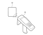
- 1 illustrates an example RFID reader according to an embodiment of the present disclosure
- FIG. FIG. 2 is a diagram illustrating an example of circuit installation according to an embodiment of the present disclosure
- FIG. 2 is a diagram illustrating an example of circuit installation according to an embodiment of the present disclosure
- FIG. 4 is a diagram showing an example of cracks
- 1 is a BB cross-sectional view of an RFID tag according to an embodiment of the present disclosure
- FIG. 2A is a cross-sectional view of a circuit according to an embodiment of the present disclosure
- FIG. 2A is a cross-sectional view of a circuit according to an embodiment of the present disclosure
- FIG. 2A is a cross-sectional view of a circuit according to an embodiment of the present disclosure
- FIG. 2A is a cross-sectional view of a circuit according to an embodiment of the present disclosure
- FIG. 1A and 1B are diagrams showing a schematic configuration of an inspection system 10 according to the first embodiment of the present disclosure.
- the inspection system 10 is applied to mobile objects.
- FIG. 1A shows an example in which an inspection system 10 is provided for a fuselage skin 20 of an aircraft 31 .
- the inspection system 10 is not limited to the aircraft 31, and can be applied to various moving bodies such as trains, spacecraft, vehicles, and watercraft.
- an inspection system 10 includes a circuit (conductive circuit, electric circuit) 11 and an RFID tag 12 as main components.
- the circuit 11 is provided on the outer surface of the moving body and is composed of conductive paint, conductive powder, metal thin film, or small-diameter metal wire. Circuit 11 is electrically conductive.
- the circuit 11 is specifically configured as follows.
- a non-conductive layer of a non-conductive coating (insulating coating) or a non-conductive coating (non-conductive oxide coating) is formed as a base material on the structural surface (outer surface) of the aircraft 31 . That is, the structural surfaces of the aircraft 31 are electrically insulated from the exterior while in intimate contact with the non-conductive layer.
- the circuit 11 is directly formed using a conductive paint on top of a non-conductive layer of non-conductive paint or non-conductive coating (outside, outside the structure of the aircraft 31), cured and adhered.
- circuit 11 is formed by a conductive powder deposited over a non-conductive layer of non-conductive paint or coating.
- circuit 11 may be formed of thin metal film or small diameter metal wire and secured by an adhesive applied over a non-conductive layer of non-conductive paint or coating. That is, the structural surface of the aircraft 31 and the circuit 11 are structurally joined while being electrically insulated by a non-conductive layer of non-conductive paint or coating.
- the circuit 11 is formed to have a predetermined circuit diagram for each part of the aircraft 31, and both ends thereof are coupled to sensor terminals of the RFID chip 14, which will be described later.
- non-conducting coatings include anodizing on aluminum alloys and passivating coatings on stainless steel, but are not limited to these.
- adhesives examples include cyanoacrylate adhesives and epoxy adhesives, but are not limited to these.
- a conductive paint is, for example, a mixture of organic paint as a solvent and graphite powder, silver powder, or a conductive polymer (a high-molecular organic compound with conductivity, a conductive molecule, or a single conductive molecule) as a solute.
- Conductive paint is in a liquid state when applied, and may be divided into a main agent and a hardener.
- a circuit pattern can be freely created according to the shape of the object to be inspected by spraying or brushing. , resulting in a solid-state circuit with Since the circuit 11 is composed of conductive paint, the circuit 11 has appropriate elasticity and adhesion to non-conductive paint or non-conductive coating, so it is resistant to slight deformation of the outer surface of the aircraft 31.
- the circuit 11 can be configured so that it does not disconnect, and the circuit 11 disconnects when there is a large deformation of the outer surface or a crack in the outer surface.
- the paint may be designed so that the circuit 11 breaks when the outer surface is deformed by a predetermined amount or more or when the outer surface is cracked.
- the circuit 11 by configuring the circuit 11 using conductive paint, conductive powder, metal thin film, or small-diameter metal wire, the elasticity of the material can be used to improve the precision (accuracy) of detection.
- the RFID tag 12 includes an RFID chip 14, an RF antenna 15, a sensor terminal 16, and a non-conductive base 17.
- the RFID chip 14 has a sensor terminal (not shown) and an antenna terminal (not shown).
- the RFID chip 14 is connected to the circuit 11 via the sensor terminal 16 and connected to the RF antenna 15 via the antenna terminal.
- RFID chip 14 detects the conduction state of circuit 11 .
- the RF antenna 15 mediates communication (signal transmission/reception) and power supply between the RFID chip 14 and the outside.
- FIG. 2 is a diagram illustrating an example when a disconnection occurs in a circuit according to an embodiment of the present disclosure.
- FIG. 2 shows a case where the circuit 11 is configured to surround the supporting portion of the window 21 in the fuselage skin 20 of the aircraft 31 .
- the supporting portion of the window 21 is also the opening of the fuselage skin 20, and stress concentration occurs.
- Circuit 11 is therefore preferably provided to pass between window 21 and fastener 22 .
- FIG. 2 shows the case where the circuit 11 is disconnected.
- a crack may occur in the outer surface of the fuselage skin 20 from the frame of the window 21 toward the fastener 22, as shown at location 23 in FIG.
- the circuit 11 is disconnected, resulting in a disconnection state.
- the RFID chip 14 detects the conduction state of the circuit 11 based on, for example, whether or not a current flows through the circuit 11 (current value), the electrical resistance value of the circuit 11, and the like.
- the continuity detection method is not limited to these.
- the continuity state is explained as whether or not the circuit 11 is disconnected, but the state between the state in which there is no disconnection and the state in which the disconnection is completely disconnected is detected as the damaged state of the circuit 11. It's good as a thing. Damage status can also be determined by the conduction status of circuit 11 .
- FIG. 7 is a BB cross-sectional view of an RFID tag according to an embodiment of the present disclosure. As shown in FIG. 7, the RF antenna 15 is held at a position appropriately spaced from the installation target surface (structure) by a non-conductive pedestal 17 . As a result, even if the installation target surface of the RFID tag 12 is a metal or CFRP conductor that does not transmit radio waves, the RF antenna 15 maintains a state in which it can transmit and receive radio waves.
- the RFID tag 12 is installed, for example, by attaching it to the outer surface of the aircraft 31 .
- the RFID tag 12 is wirelessly supplied with power from an RFID reader 13, which will be described later. This power is used to detect the conduction state of the circuit 11, and the detection result is sent to the RFID reader 13 together with the unique identification information in the RFID chip 14. to send.
- the RFID chip 14 is provided with an anti-interference device, and even if a plurality of RFID tags 12 exist within the radio wave transmission range of the RFID reader 13, the RFID reader 13 can read them all at once.
- the RFID reader 13 wirelessly supplies power to the RFID tag 12 and receives information from the RFID tag 12 . Specifically, power is supplied from the RFID reader 13 to the RFID tag 12, and an instruction signal is transmitted to the RFID tag 12 to detect the conduction state of the circuit 11 and transmit the detection result. Along with this, the RFID chip 14 constituting the RFID tag 12 is charged with the received power, performs detection processing according to the instruction signal, and collects the detection result together with the unique identification information in the RFID chip 14 to the RFID reader 13. Send. As a result, the RFID reader 13 can read the conduction state of the circuit 11 detected by the RFID tag 12 at a specific location.
- the outer surface of the aircraft 31 is coated with a non-conductive paint (such as an insulating rust-preventive paint) or a non-conductive coating to form an insulating region for the outer surface as a base (non-conductive layer). Then, a circuit 11 is formed on this insulating area and an RFID tag 12 is installed. Circuit 11 is adhered to the outer surface of aircraft 31 . Therefore, a non-conductive layer, a layer of the circuit 11 and the RFID tag 12, and a non-conductive atmosphere are laminated in this order from the outer surface of the aircraft 31 toward the outside. That is, the circuit 11 is electrically insulated by a non-conductive member.
- a non-conductive paint such as an insulating rust-preventive paint
- a non-conductive coating such as an insulating rust-preventive paint
- FIG. 8 is a cross-sectional view AA of a circuit according to one embodiment of the present disclosure.
- the circuit 11 shown in FIG. 8 is formed by a conductive paint or conductive powder on top of a non-conductive layer (outside, outside the structure of the aircraft 31) of non-conductive paint or coating.
- FIG. 9 is a cross-section AA of a circuit according to one embodiment of the present disclosure.
- the circuit 11 shown in FIG. 9 is formed of a metal thin film or a small-diameter metal wire.
- FIG. 10 is a cross-sectional view AA of a circuit according to one embodiment of the present disclosure.
- the circuit 11 shown in FIG. 10 is formed by a conductive paint or powder on top of a non-conductive layer (outside, outside the structure of the aircraft 31) of non-conductive paint or coating. The entire circuit 11 is covered with non-conductive paint for structural protection.
- FIG. 11 is a cross-sectional view AA of a circuit according to one embodiment of the present disclosure.
- circuit 11 is formed by a metal thin film or a small-diameter metal wire.
- Circuit 11 is secured by an adhesive applied over a non-conductive layer of non-conductive paint or coating.
- the entire circuit 11 is covered with non-conductive paint for structural protection.
- the surface can be smoothed by suppressing steps while maintaining an economically valuable appearance. Therefore, it can be applied to moving objects sensitive to the influence of air resistance (for example, high-speed moving objects) and to moving objects whose appearance is important (for example, sports cars).
- a predetermined area including the installation area of the circuit 11 and the RFID tag 12 and other areas may be covered with a continuous non-conductive heat insulating material for heat retention. While maintaining the thermal environment inside the moving body, the surface can be smoothed by suppressing steps. Therefore, it can be applied to mobile objects (such as rockets and hydrogen aircraft) that are sensitive to the effects of air resistance.
- Non-conductive paints for structural protection include, but are not limited to, polyurethane enamels and epoxy primers.
- non-conductive heat insulating materials for heat retention include urethane foam heat insulating materials and glass wool, but are not limited to these.
- the RFID tag 12 It is preferable to mark the position where the RFID tag 12 is installed after covering it with a non-conductive paint for structural protection so that it can be recognized from the outside. Moreover, it is preferable to record in advance a combination of the installation position of the RFID tag 12 and the unique identification information in the RFID chip 14 of the RFID tag 12 .
- the circuit 11 Since the inspection system 10 detects damage to the outer surface of the aircraft 31, the circuit 11 is preferably located where damage is expected to occur.
- the places where damage is likely to occur are, for example, cutout positions (ends of members) and places where high stress occurs (places where stress concentration tends to occur). In other words, it is preferable to provide the circuit 11 around the cutout position and the stress concentrated portion.
- FIG. 4 is a diagram showing an example when the circuit 11 is installed on the aircraft 31.
- FIG. 4 shows an example of a circuit 11 provided around a cut-out location in the aircraft structure.
- the circuit 11 includes a window (for example, a cabin window) 21 of an aircraft 31, a cockpit windshield 24 of the aircraft 31, a door (door) 25, a door (emergency exit) 26, and an antenna attachment point on an outer surface. 27.
- the circuit 11 may be provided so as to pass through the vicinity of the fastener fastening portion (fastener portion) 28 on the outer surface (the range where the crack is expected to grow).
- the fastener fastening portion 28 is a joint portion between members constituting the aircraft 31, and particularly refers to a portion around an opening opened in the member and a portion provided with the fastener 22 to be inserted therein.
- FIG. 5 is a diagram showing an example in which the circuit 11 is installed on the aircraft 31.
- FIG. 5 is a view of the aircraft 31 viewed from below.
- FIG. 5 shows an example in which a circuit 11 is provided around a stress concentration point in an aircraft structure.
- the circuit 11 is provided so as to surround the manhole 41 .
- the circuit 11 is provided so as to pass through the vicinity (range where crack growth is expected) of each of the connecting portion 42 of the wing body, the mounting portion 43 of the landing gear, and the fitting portion 44 .
- the manhole 41 is an opening for accessing the inside and is closed with a lid.
- the metal fittings are metal fittings attached to the aircraft 31 .
- the neighborhood is a range of 2.5 cm from the end (or joint) of the part where the circuit 11 is provided.
- Fig. 6 shows an example of cracks.
- the circuit 11 is disconnected due to the damage and detected by the RFID tag 12 .
- the installation location of the circuit 11 illustrated in FIGS. 4 and 5 is not limited to the aircraft 31 and may be applied to other moving bodies as long as they have the same configuration. Also, the position where the circuit 11 is installed is not limited to the outer surface, and it may be installed inside the mobile structure.
- circuit 11 made of conductive paint, conductive powder, a metal thin film, or a small-diameter metal wire and an RFID tag 12
- protrusions on the outer surface of the moving body are minimized to suppress an increase in air resistance of the moving body. be able to.
- the circuit 11 is cut along the outer surface of the moving body by forming the circuit 11 with conductive paint, conductive powder, metal thin film, or small-diameter metal wire.
- the elasticity of the material maintains the conductive state of the circuit 11, thereby suppressing erroneous detection of damage.
- the circuit 11, the RFID tag 12, and a predetermined area around the circuit 11 and the RFID tag 12 on the outer surface of the moving body and other areas are continuously covered with an exterior material such as non-conductive paint or non-conductive heat insulating material. Therefore, it is possible to suppress steps on the surface and smooth the surface. In addition, both are possible without impairing economic efficiency and functionality such as appearance and heat insulation.
- An inspection system includes a conductive circuit provided on an insulating paint or a non-conductive film on a structural surface of a moving body and in close contact with the insulating paint or the non-conductive film; and a sensor connected to the conductive circuit. and an RF antenna terminal connected to an RF antenna, and an RFID IC chip for detecting the conduction state of a conductive circuit. Therefore, by detecting the conduction state (disconnection, resistance, etc.) of the conductive circuit with the RFID chip, it is possible to detect the state of cracks on the surface of the moving body. Since the status can be read by the RFID chip, inspection can be made more efficient. It is possible to increase the frequency of inspections, and an improvement in safety can be expected. In addition, since the non-conductive pedestal holds the sensor terminal, the RF antenna and the RFID chip, remote inspection using the RFID reader and the RFID chip is possible even for an object to be inspected, such as metal or CFRP, which does not transmit radio waves.
- the conductive circuit and the RFID chip provided on the insulating paint or the non-conductive film on the structural surface of the moving object and in close contact with the insulating paint or the non-conductive film the step on the surface of the moving object is suppressed. It is possible to suppress an increase in air resistance of the moving body.
- the insulating paint or non-conductive coating may have interfacial strength to adhere to the moving object.
- the insulating paint or non-conductive coating has an interfacial strength such that the insulating paint or non-conductive coating adheres to the moving body, so that the insulating coating or non-conductive coating is a layer that protects the structure of the moving body from corrosion and external damage. can be configured.
- the conductive circuit is formed by a conductive paint that is an organic compound solvent that uses conductive molecules or conductive single atoms as a solute and adheres to the insulating paint or non-conductive film when cured.
- a conductive paint that is an organic compound solvent that uses conductive molecules or conductive single atoms as a solute and adheres to the insulating paint or non-conductive film when cured.
- the conductive circuit can be attached to an insulating paint or a non-conductive coating, and is formed of a conductive powder in which conductive molecules or conductive single atoms account for 50% or more of the composition. may be
- a conductive circuit can be attached to an insulating paint or a non-conductive coating, and is formed of a conductive powder in which conductive molecules or conductive single atoms account for 50% or more of the composition. This creates a circuit that has the property of being adherent as it is formed, in addition to being conductive.
- the conductive circuit is formed by a metal thin film with a thickness of 70 ⁇ m or less or a metal wire with a diameter of 200 ⁇ m or less bonded to an insulating paint or non-conductive coating via an adhesive. Therefore, it is possible to control the dimension of the metal thin film or metal wire to a certain level or less so that the interface strength of the adhesive is superior, and to ensure the detection of damage.
- the RFID chip may receive power and transmit and receive signals wirelessly via an RF antenna to detect whether or not a conductive circuit is disconnected.
- the inspection system it is possible to detect cracks on the surface of the mobile object by detecting whether or not the RFID chip has caused a circuit breakage.
- the surface of the moving object is smoothed by suppressing steps.
- the RFID reader can read the conduction state of the conductive circuit detected by the RFID chip.
- the inspection system according to the present disclosure may include a non-conductive pedestal that holds the RF antenna and the RFID chip. According to the inspection system according to the present disclosure, since a non-conductive pedestal with appropriate dimensions is applied between the RF antenna and the structure to be inspected, even an inspection object such as metal or CFRP that does not transmit radio waves can be used as an RFID reader. Remote inspection using the RFID chip becomes possible, and power reception and signal transmission/reception capability from the RF reader can be improved.
Landscapes
- Engineering & Computer Science (AREA)
- Physics & Mathematics (AREA)
- General Physics & Mathematics (AREA)
- Aviation & Aerospace Engineering (AREA)
- Computer Hardware Design (AREA)
- Microelectronics & Electronic Packaging (AREA)
- Theoretical Computer Science (AREA)
- Mechanical Engineering (AREA)
- Manufacturing & Machinery (AREA)
- Transportation (AREA)
- Investigating Or Analyzing Materials By The Use Of Electric Means (AREA)
Abstract
[Problem] To provide an inspection system with which it is possible to achieve the accuracy of detection suitable for the maintenance of structural soundness while reducing costs by circuit simplification and suppressing an interference with structures in the surrounding of an installed place, an increase in air resistance, and an impact on external appearance. [Solution] An inspection system (10) applied to moving vehicles, comprising a circuit (11) provided on the insulating coating or non-conducting coating of the structural surface of a moving vehicle and closely attached to the insulating coating or the non-conducting coating, a sensor terminal connected to the circuit (11), and an RF antenna terminal connected to an RF antenna (15), and further including an RFID IC chip (14) for detecting the electrical continuity state of the circuit (11).
Description
本開示は、検査システムに関するものである。
This disclosure relates to an inspection system.
旅客機等の航空機は、運行中の健全性が担保するために、定期点検が実施される。定期点検は、検査員等により外観を目視することで行われる。特許文献1及び特許文献2では、RFID等を用いて欠陥検出を行うことが開示されている。
Aircraft such as passenger aircraft undergo regular inspections to ensure their soundness during operation. Periodic inspection is performed by visual inspection by an inspector or the like. Patent Documents 1 and 2 disclose defect detection using an RFID or the like.
航空機は、飛行回数の増加に伴い疲労やダメージが蓄積してゆくため、機体ごとに決まったインターバルでの点検が義務付けられている。主な点検方法である目視点検では、点検対象数と点検頻度に比例した手間と時間を要する。また機体の軽量化を進めると、燃費は良くなるが、部材毎の負担する応力は増加し疲労やダメージが蓄積しやすくなる。この場合、健全性の維持には頻繁な点検を要することとなり、運用コストに跳ね返る。逆に、高い損傷許容強度を持つように設計すると、点検頻度を増加させずに健全性の維持改善ができる。しかし、機体全体の重量増加や燃費悪化などの機体性能の悪化につながる。そのため、現在の航空機構造は点検の負担と機体性能との妥協点を狙って設計する事となるが、更なる性能向上のためには点検の負担軽減が必要である。
Because aircraft fatigue and damage accumulate as the number of flights increases, inspections are required at fixed intervals for each aircraft. Visual inspection, which is the main inspection method, requires labor and time proportional to the number of objects to be inspected and the inspection frequency. Also, if the weight of the airframe is reduced, the fuel consumption will be improved, but the stress that each member will bear will increase, and fatigue and damage will easily accumulate. In this case, maintenance of soundness requires frequent inspections, which increases operating costs. Conversely, if it is designed to have a high damage tolerance strength, soundness can be maintained and improved without increasing the frequency of inspections. However, it leads to deterioration of aircraft performance such as increased weight of the entire aircraft and deterioration of fuel efficiency. Therefore, the current aircraft structure is designed aiming at a compromise between the burden of inspection and airframe performance, but in order to further improve performance, it is necessary to reduce the burden of inspection.
特許文献1ではRFIDで欠陥検出を行うことが記載されているものの、非破壊検査を用いた方法であり、航空機などの移動体構造における数ミリ単位の損傷を正確に検出できる精度は望めない。
また、特許文献2でも導体回路の破壊を伴う損傷検出方法と無線通信装置との組み合わせを提案しているが、導体回路を絶縁膜でサンドイッチ又は被覆した検出装置を用いており、装置作成には手間を要する。
また、特許文献2では、絶縁膜と導体回路の強度や、それらの界面や関係性について具体的に開示されていない。例えば導体回路の強度よりも絶縁膜や界面の強度が弱いと、母材に損傷が発生しても絶縁体内または界面での損傷が拡大するだけであり、導体回路まで損傷を伝播させきれず、望ましい精度での損傷検出ができるとは限らない。このため、検出回路の素材や構成要素の断面形状には改善の余地がある。
また、回路の寸法についての具体的な値の開示がないため、設置対象の外側に突出することで、空気抵抗の増加や周辺構造物との干渉や外観の悪化を誘発する可能性もある。
また、回路に繋がれたセンサを駆動させるためにトランスポンダとは別にレシーバを用意して電力供給をしなければならないため、構成部材が多く複雑かつ大型になる。このため、システムの簡素化や低コスト化に改善の余地がある。またその一方で、RFIDタグを構成するRFアンテナを金属やCFRP等の導電体の至近位置に設置すると、RFIDリーダから発せられる電波がRFアンテナに貫入せず、通信が成立しない等の課題を内包している。 Although Patent Document 1 describes that defect detection is performed by RFID, it is a method using non-destructive inspection, and accuracy that can accurately detect damage on the order of several millimeters in a moving body structure such as an aircraft cannot be expected.
In addition, Patent Document 2 also proposes a combination of a damage detection method involving destruction of a conductor circuit and a wireless communication device. It takes time.
Moreover, Patent Document 2 does not specifically disclose the strength of the insulating film and the conductor circuit, their interfaces, and their relationship. For example, if the strength of the insulating film or interface is weaker than the strength of the conductor circuit, even if damage occurs in the base material, the damage will only spread within the insulator or at the interface, and the damage will not be able to propagate to the conductor circuit. It is not always possible to detect damage with the desired accuracy. Therefore, there is room for improvement in the materials of the detection circuit and the cross-sectional shapes of the components.
In addition, since there is no disclosure of specific values for circuit dimensions, there is a possibility that protruding outside the installation target will increase air resistance, interfere with surrounding structures, and cause deterioration in appearance.
In addition, in order to drive the sensor connected to the circuit, it is necessary to prepare a receiver separate from the transponder and supply power. Therefore, there is room for improvement in simplification and cost reduction of the system. On the other hand, if the RF antenna that constitutes the RFID tag is placed in close proximity to a conductor such as metal or CFRP, the radio waves emitted from the RFID reader will not penetrate the RF antenna and communication will not be established. are doing.
本開示は、このような事情に鑑みてなされたものであって、回路の簡素化によるコスト低減、設置個所周辺の構造物との干渉、空気抵抗の増加および外観への影響を抑制しながら、構造健全性の維持に適した検出精度を達成することができる検査システムを提供することを目的とする。
The present disclosure has been made in view of such circumstances, and while suppressing cost reduction due to circuit simplification, interference with structures around the installation location, increase in air resistance, and appearance, An object of the present invention is to provide an inspection system capable of achieving detection accuracy suitable for maintaining structural integrity.
本開示の第1態様は、移動体に適用される検査システムであって、前記移動体の構造表面の絶縁性塗料上または不導体被膜上に設けられ、該絶縁性塗料または該不導体被膜と密着した導電性回路と、前記導電性回路に接続されるセンサ端子と、RFアンテナに接続されるRFアンテナ端子とを備え、前記導電性回路の導通状態を検出するRFIDICチップと、を備える検査システムである。
A first aspect of the present disclosure is an inspection system applied to a moving body, provided on an insulating coating or a non-conductive coating on the structural surface of the moving body, and the insulating coating or the non-conductive coating An inspection system comprising: an RFID IC chip that includes a closely attached conductive circuit, a sensor terminal connected to the conductive circuit, and an RF antenna terminal connected to an RF antenna, and detects a continuity state of the conductive circuit. is.
本開示によれば、検査システムの導体性回路の素材・形状・強度を調整し、特定の導電性塗料または導電性粉末または接着剤を用いて移動体表面に密着した導電性回路を敷設し、検査システムの損傷検出精度を向上することができるという効果を奏する。また、検査システムに使用する導電性回路が薄い又は細いことで、回路設置時の周辺構造物への干渉、空気抵抗の増加および外観の悪化を抑制することができるという効果を奏する。また、検査システムに使用するRFIDICチップが通信機能及び損傷検出回路の検査機能を持つため、装置全体の簡素化、軽量化および小型化が実現できるという効果を奏する。また、金属やCFRP等の電波を通さない検査対象でも、RFIDリーダとRFIDICチップを利用した遠隔検査が可能となるという効果を奏する。
According to the present disclosure, adjusting the material, shape, and strength of the conductive circuit of the inspection system, laying the conductive circuit in close contact with the surface of the moving object using a specific conductive paint, conductive powder, or adhesive, This has the effect of improving the damage detection accuracy of the inspection system. In addition, since the conductive circuit used in the inspection system is thin or narrow, it is possible to suppress interference with surrounding structures, increase in air resistance, and deterioration in appearance when the circuit is installed. Moreover, since the RFID chip used in the inspection system has a communication function and an inspection function of the damage detection circuit, there is an effect that the simplification, weight reduction, and miniaturization of the entire device can be realized. In addition, there is an effect that remote inspection using an RFID reader and an RFID chip is possible even for an object to be inspected, such as metal or CFRP, which does not transmit radio waves.
以下に、本開示に係る検査システムの一実施形態について、図面を参照して説明する。
An embodiment of an inspection system according to the present disclosure will be described below with reference to the drawings.
図1A及び図1Bは、本開示の第1実施形態に係る検査システム10の概略構成を示す図である。検査システム10は、移動体に適用される。本実施形態では、移動体として航空機31に検査システム10が適用される場合を一例として説明する。図1Aは、航空機31の胴体外板20に対して検査システム10を設けた場合を例としている。なお、検査システム10は、航空機31に限定されず、列車や宇宙機、車両、水上船舶等の様々な移動体に適用することも可能である。
1A and 1B are diagrams showing a schematic configuration of an inspection system 10 according to the first embodiment of the present disclosure. The inspection system 10 is applied to mobile objects. In this embodiment, a case in which the inspection system 10 is applied to an aircraft 31 as a moving object will be described as an example. FIG. 1A shows an example in which an inspection system 10 is provided for a fuselage skin 20 of an aircraft 31 . Note that the inspection system 10 is not limited to the aircraft 31, and can be applied to various moving bodies such as trains, spacecraft, vehicles, and watercraft.
図1Bに示すように、本実施形態に係る検査システム10は、回路(導電性回路、電気回路)11と、RFIDタグ12とを主な構成として備えている。
As shown in FIG. 1B, an inspection system 10 according to this embodiment includes a circuit (conductive circuit, electric circuit) 11 and an RFID tag 12 as main components.
回路11は、移動体の外表面に対して設けられ、導電性塗料、導電性粉末、金属薄膜または小径金属ワイヤにより構成される。回路11は導電性を有する。
The circuit 11 is provided on the outer surface of the moving body and is composed of conductive paint, conductive powder, metal thin film, or small-diameter metal wire. Circuit 11 is electrically conductive.
回路11は、具体的に次のように構成される。
航空機31の構造表面(外表面)に対して、下地材として非導電性塗料(絶縁性塗料)または不導体被膜(不導体酸化被膜)による非導電性の層が構成される。すなわち、航空機31の構造表面は、非導電性の層と密着しながら、その外側とは電気的に絶縁される。 Thecircuit 11 is specifically configured as follows.
A non-conductive layer of a non-conductive coating (insulating coating) or a non-conductive coating (non-conductive oxide coating) is formed as a base material on the structural surface (outer surface) of theaircraft 31 . That is, the structural surfaces of the aircraft 31 are electrically insulated from the exterior while in intimate contact with the non-conductive layer.
航空機31の構造表面(外表面)に対して、下地材として非導電性塗料(絶縁性塗料)または不導体被膜(不導体酸化被膜)による非導電性の層が構成される。すなわち、航空機31の構造表面は、非導電性の層と密着しながら、その外側とは電気的に絶縁される。 The
A non-conductive layer of a non-conductive coating (insulating coating) or a non-conductive coating (non-conductive oxide coating) is formed as a base material on the structural surface (outer surface) of the
回路11は、非導電性塗料または不導体被膜による非導電性の層の上(外側、航空機31の構造の外側)に導電性塗料を用いて直接形成され、硬化および密着される。または、回路11は、非導電性塗料または不導体被膜による非導電性の層の上に付着する導電性粉末により形成される。または、回路11は、金属薄膜または小径金属ワイヤで形成され、非導電性塗料または不導体被膜による非導電性の層の上に塗布された接着剤により、固定される。すなわち、航空機31の構造表面と回路11とは、非導電性塗料または不導体被膜による非導電性の層により電気的に絶縁されながら、構造的には接合された状態となる。回路11は、航空機31の部位ごとに所定の回路図となるように形成され、その両端部は後述するRFIDICチップ14のセンサ端子と結合される。
The circuit 11 is directly formed using a conductive paint on top of a non-conductive layer of non-conductive paint or non-conductive coating (outside, outside the structure of the aircraft 31), cured and adhered. Alternatively, circuit 11 is formed by a conductive powder deposited over a non-conductive layer of non-conductive paint or coating. Alternatively, circuit 11 may be formed of thin metal film or small diameter metal wire and secured by an adhesive applied over a non-conductive layer of non-conductive paint or coating. That is, the structural surface of the aircraft 31 and the circuit 11 are structurally joined while being electrically insulated by a non-conductive layer of non-conductive paint or coating. The circuit 11 is formed to have a predetermined circuit diagram for each part of the aircraft 31, and both ends thereof are coupled to sensor terminals of the RFID chip 14, which will be described later.
不導体被膜として、例えばアルミニウム合金におけるアノダイズ処理や、ステンレス鋼におけるパシベート被膜が挙げられるが、これに限られるものではない。
Examples of non-conducting coatings include anodizing on aluminum alloys and passivating coatings on stainless steel, but are not limited to these.
非導電性塗料として、例えばエポキシプライマやポリウレタンエナメルトップコートが挙げられるが、これに限られるものではない。
Non-conductive paints include, but are not limited to, epoxy primers and polyurethane enamel topcoats.
接着剤として、例えばシアノアクリレート接着剤やエポキシ接着剤が挙げられるが、これに限られるものではない。
Examples of adhesives include cyanoacrylate adhesives and epoxy adhesives, but are not limited to these.
導電性塗料は、例えば有機塗料を溶媒として、黒鉛粉または銀粉または導電性ポリマー(導電性を有する高分子有機化合物、導電性分子または導電性単体分子)が溶質として配合されたものである。導電性塗料は、塗付時には液体状であり、主剤と硬化剤とに分かれていてもよく、スプレーや刷毛で検査対象の形状に応じた回路パターンを自由に作成でき、その硬化後は導電性を有する固体回路となる。導電性の塗料により回路11が構成されることで、回路11が適度な弾性と非導電性塗料または不導体被膜への密着性を持つため、航空機31の外表面の軽微な変形に対しては回路11が断線せず、外表面の大きな変形や外表面の亀裂に対しては回路11が断線するように構成することができる。外表面が所定の変形量以上に変形した場合または外表面に亀裂が発生した場合に対して回路11が断線するように塗料を設計してもよい。
A conductive paint is, for example, a mixture of organic paint as a solvent and graphite powder, silver powder, or a conductive polymer (a high-molecular organic compound with conductivity, a conductive molecule, or a single conductive molecule) as a solute. Conductive paint is in a liquid state when applied, and may be divided into a main agent and a hardener. A circuit pattern can be freely created according to the shape of the object to be inspected by spraying or brushing. , resulting in a solid-state circuit with Since the circuit 11 is composed of conductive paint, the circuit 11 has appropriate elasticity and adhesion to non-conductive paint or non-conductive coating, so it is resistant to slight deformation of the outer surface of the aircraft 31. The circuit 11 can be configured so that it does not disconnect, and the circuit 11 disconnects when there is a large deformation of the outer surface or a crack in the outer surface. The paint may be designed so that the circuit 11 breaks when the outer surface is deformed by a predetermined amount or more or when the outer surface is cracked.
導電性粉末は、不導体被膜上または非導電性塗料上に付着することのできる導電性分子または導電性単体原子がその組成の50%以上を占める粉末で構成されたものである。導電性の粉末により回路11が構成されることで、回路11が適度な弾性と非導電性塗料または不導体被膜への密着性を持つため、航空機31の外表面の軽微な変形に対しては回路11が断線せず、外表面の大きな変形や外表面の亀裂に対しては回路11が断線するように構成することができる。外表面が所定の変形量以上に変形した場合または外表面に亀裂が発生した場合に対して回路11が断線するように塗料を設計してもよい。
The conductive powder is composed of a powder in which 50% or more of the composition is composed of conductive molecules or conductive single atoms that can adhere to the non-conductive coating or non-conductive paint. Since the circuit 11 is composed of conductive powder, the circuit 11 has moderate elasticity and adhesion to non-conductive paint or non-conductive coating, so it is resistant to slight deformation of the outer surface of the aircraft 31. The circuit 11 can be configured so that it does not disconnect, and the circuit 11 disconnects when there is a large deformation of the outer surface or a crack in the outer surface. The paint may be designed so that the circuit 11 breaks when the outer surface is deformed by a predetermined amount or more or when the outer surface is cracked.
金属薄膜は、例えば検査対象の構造材料と似た弾性や強度をもつ材料で構成される。具体的には、アルミニウムやその合金や銅製である。形状は薄い箔やメッシュといった薄い形状である。航空機31に課される目視点検で発見可能なサイズの亀裂までも精度よく検知できるように、その断面厚さは100μm以内である。適切な材料特性と形状を持つ金属薄膜により回路11が構成され、接着剤を介して航空機31の外表面に密着することで、航空機31の外表面の軽微な変形に対しては回路11が断線せず、外表面の大きな変形や外表面の亀裂に対しては回路11が断線するように構成することができる。外表面が所定の変形量以上に変形した場合または外表面に亀裂が発生した場合に対して回路11が断線するように金属薄膜を設計してもよい。
For example, the metal thin film is composed of a material with elasticity and strength similar to the structural material to be inspected. Specifically, it is made of aluminum, its alloy, or copper. The shape is a thin shape such as a thin foil or mesh. The cross-sectional thickness is within 100 μm so that even a crack of a size that can be detected by visual inspection imposed on the aircraft 31 can be accurately detected. The circuit 11 is composed of a metal thin film with appropriate material properties and shape, and is adhered to the outer surface of the aircraft 31 via an adhesive, so that the circuit 11 is disconnected even if the outer surface of the aircraft 31 is slightly deformed. Instead, the circuit 11 can be configured to disconnect in response to a large deformation of the outer surface or a crack in the outer surface. The metal thin film may be designed so that the circuit 11 is disconnected when the outer surface is deformed by a predetermined amount or more or when the outer surface is cracked.
小径金属ワイヤは、例えば銅やアルミニウム製の細い線である。断面は円形であるが、多角形や中空のものでもよい。複数の小径金属ワイヤを撚り合わせたものでもよい。表面に絶縁層を有していてもよい。適切な弾性を持つ小径金属ワイヤにより回路11が構成され、接着剤を介して航空機31の外表面に密着することで、航空機31の外表面の軽微な変形に対しては回路11が断線せず、外表面の大きな変形や外表面の亀裂に対しては回路11が断線するように構成することができる。また、外表面が所定の変形量以上に変形した場合または外表面に亀裂が発生した場合に対して回路11が断線するように小径金属ワイヤを設計してもよい。
A small-diameter metal wire is, for example, a thin wire made of copper or aluminum. Although the cross section is circular, it may be polygonal or hollow. A plurality of small-diameter metal wires twisted together may also be used. You may have an insulating layer on the surface. The circuit 11 is composed of a small-diameter metal wire having appropriate elasticity, and is adhered to the outer surface of the aircraft 31 via an adhesive, so that the circuit 11 will not disconnect even if the outer surface of the aircraft 31 is slightly deformed. , the circuit 11 can be configured to disconnect in response to a large deformation of the outer surface or a crack in the outer surface. Also, the small-diameter metal wire may be designed so that the circuit 11 is disconnected when the outer surface is deformed by a predetermined amount or more or when the outer surface is cracked.
このように、導電性塗料、導電性粉末、金属薄膜または小径金属ワイヤを用いて回路11を構成することで、材料の弾性を利用して検出の精度(正確性)を向上させることができる。
In this way, by configuring the circuit 11 using conductive paint, conductive powder, metal thin film, or small-diameter metal wire, the elasticity of the material can be used to improve the precision (accuracy) of detection.
RFIDタグ12は、RFIDICチップ14と、RFアンテナ15とセンサ端子16と不導体台座17を備える。RFIDICチップ14は、センサ端子(図示せず)およびアンテナ端子(図示せず)を備える。RFIDICチップ14は、センサ端子16を介して回路11と接続され、アンテナ端子を介してRFアンテナ15と接続される。RFIDICチップ14は、回路11の導通状態を検出する。RFアンテナ15は、RFIDICチップ14と外部との通信(信号送受信)および電力供給を媒介する。
The RFID tag 12 includes an RFID chip 14, an RF antenna 15, a sensor terminal 16, and a non-conductive base 17. The RFID chip 14 has a sensor terminal (not shown) and an antenna terminal (not shown). The RFID chip 14 is connected to the circuit 11 via the sensor terminal 16 and connected to the RF antenna 15 via the antenna terminal. RFID chip 14 detects the conduction state of circuit 11 . The RF antenna 15 mediates communication (signal transmission/reception) and power supply between the RFID chip 14 and the outside.
図2は、本開示の一実施形態に係る回路に断線が発生した場合の例を示す図である。
図2は、航空機31の胴体外板20において、窓21の支持部分を囲むように回路11を構成した場合を示している。窓21の支持部分は胴体外板20の開口部でもあり、応力集中が発生する。かつ胴体外板20と窓21とを締結するファスナ22用の穴があり、亀裂が発生しやすい箇所である。よって回路11は、窓21とファスナ22の間を通過するように設けられることが好ましい。 FIG. 2 is a diagram illustrating an example when a disconnection occurs in a circuit according to an embodiment of the present disclosure.
FIG. 2 shows a case where thecircuit 11 is configured to surround the supporting portion of the window 21 in the fuselage skin 20 of the aircraft 31 . The supporting portion of the window 21 is also the opening of the fuselage skin 20, and stress concentration occurs. In addition, there is a hole for the fastener 22 that fastens the fuselage outer plate 20 and the window 21, which is a location where cracks are likely to occur. Circuit 11 is therefore preferably provided to pass between window 21 and fastener 22 .
図2は、航空機31の胴体外板20において、窓21の支持部分を囲むように回路11を構成した場合を示している。窓21の支持部分は胴体外板20の開口部でもあり、応力集中が発生する。かつ胴体外板20と窓21とを締結するファスナ22用の穴があり、亀裂が発生しやすい箇所である。よって回路11は、窓21とファスナ22の間を通過するように設けられることが好ましい。 FIG. 2 is a diagram illustrating an example when a disconnection occurs in a circuit according to an embodiment of the present disclosure.
FIG. 2 shows a case where the
上述した様に、図2は、回路11に断線が発生した場合を示している。例えば、図2の箇所23で示すように、窓21の枠からファスナ22に向かって胴体外板20の外表面に亀裂が発生する。すると、これに伴って回路11が切断し、断線状態となる。
As described above, FIG. 2 shows the case where the circuit 11 is disconnected. For example, a crack may occur in the outer surface of the fuselage skin 20 from the frame of the window 21 toward the fastener 22, as shown at location 23 in FIG. As a result, the circuit 11 is disconnected, resulting in a disconnection state.
このように、航空機31の外表面に亀裂が発生すると、回路11が切断される。
Thus, when a crack occurs on the outer surface of the aircraft 31, the circuit 11 is cut.
RFIDタグ12のRFIDICチップ14は、センサ端子16を介して回路11の2つの端部に接続されて回路11と閉回路を構成する。そして、回路11の導通状態を検出する。回路11の導通状態とは、例えば回路11に切断が発生しているか否かである。すなわち、RFIDICチップ14は、回路11に切断が生じているか否かを検出する。RFIDICチップ14が回路11に切断が生じているか否かを検出することで、回路11の切断の原因である航空機31の外表面の亀裂を検出することができる。
The RFID chip 14 of the RFID tag 12 is connected to the two ends of the circuit 11 through the sensor terminals 16, forming a closed circuit with the circuit 11. Then, the conduction state of the circuit 11 is detected. The conduction state of the circuit 11 is, for example, whether or not the circuit 11 is disconnected. That is, the RFID chip 14 detects whether or not the circuit 11 is disconnected. By detecting whether or not the circuit 11 is disconnected, the RFID chip 14 can detect cracks on the outer surface of the aircraft 31 that are the cause of the disconnection of the circuit 11 .
RFIDICチップ14は、例えば回路11に電流が流れるか否か(電流値)や、回路11の電気抵抗値等により、回路11の導通状態を検出する。導通状態の検出方法はこれらに限定されない。
The RFID chip 14 detects the conduction state of the circuit 11 based on, for example, whether or not a current flows through the circuit 11 (current value), the electrical resistance value of the circuit 11, and the like. The continuity detection method is not limited to these.
上記の例では、導通状態を、回路11が切断しているか否かとして説明したが、切断が発生していない状態から完全に切断となる状態の間の状態を回路11の損傷状態として検出することとしても良い。損傷状態についても回路11の導通状態により判断することができる。
In the above example, the continuity state is explained as whether or not the circuit 11 is disconnected, but the state between the state in which there is no disconnection and the state in which the disconnection is completely disconnected is detected as the damaged state of the circuit 11. It's good as a thing. Damage status can also be determined by the conduction status of circuit 11 .
RFIDICチップ14のアンテナ端子にはRFアンテナ15が接続され、RFアンテナ15はRFIDタグ12と同様にシート状の部材であり、RFIDタグ12を構成する。
図7は、本開示の一実施形態に係るRFIDタグのB-B断面図である。図7に示されるように、RFアンテナ15は、不導体台座17により設置対象面(構造)から適切な間隔をとった位置に保持される。これにより、RFIDタグ12の設置対象面が電波を通さない金属製やCFRP製の導電体であっても、RFアンテナ15が電波を授受できる状態を保つ。
RFIDタグ12は、例えば航空機31の外表面に張り付けることで設置される。RFIDタグ12は、後述するRFIDリーダ13から無線で電力供給がされ、この電力によって回路11の導通状態の検出処理を実行し、RFIDリーダ13へ検出結果をRFIDICチップ14内の固有識別情報とあわせて送信する。RFIDICチップ14には混信防止装置が備えられ、RFIDリーダ13の電波送信範囲に複数のRFIDタグ12が存在しても、RFIDリーダ13側では一括での読み取りが可能である。 AnRF antenna 15 is connected to an antenna terminal of the RFID chip 14 . The RF antenna 15 is a sheet-like member similar to the RFID tag 12 and constitutes the RFID tag 12 .
FIG. 7 is a BB cross-sectional view of an RFID tag according to an embodiment of the present disclosure. As shown in FIG. 7, theRF antenna 15 is held at a position appropriately spaced from the installation target surface (structure) by a non-conductive pedestal 17 . As a result, even if the installation target surface of the RFID tag 12 is a metal or CFRP conductor that does not transmit radio waves, the RF antenna 15 maintains a state in which it can transmit and receive radio waves.
TheRFID tag 12 is installed, for example, by attaching it to the outer surface of the aircraft 31 . The RFID tag 12 is wirelessly supplied with power from an RFID reader 13, which will be described later. This power is used to detect the conduction state of the circuit 11, and the detection result is sent to the RFID reader 13 together with the unique identification information in the RFID chip 14. to send. The RFID chip 14 is provided with an anti-interference device, and even if a plurality of RFID tags 12 exist within the radio wave transmission range of the RFID reader 13, the RFID reader 13 can read them all at once.
図7は、本開示の一実施形態に係るRFIDタグのB-B断面図である。図7に示されるように、RFアンテナ15は、不導体台座17により設置対象面(構造)から適切な間隔をとった位置に保持される。これにより、RFIDタグ12の設置対象面が電波を通さない金属製やCFRP製の導電体であっても、RFアンテナ15が電波を授受できる状態を保つ。
RFIDタグ12は、例えば航空機31の外表面に張り付けることで設置される。RFIDタグ12は、後述するRFIDリーダ13から無線で電力供給がされ、この電力によって回路11の導通状態の検出処理を実行し、RFIDリーダ13へ検出結果をRFIDICチップ14内の固有識別情報とあわせて送信する。RFIDICチップ14には混信防止装置が備えられ、RFIDリーダ13の電波送信範囲に複数のRFIDタグ12が存在しても、RFIDリーダ13側では一括での読み取りが可能である。 An
FIG. 7 is a BB cross-sectional view of an RFID tag according to an embodiment of the present disclosure. As shown in FIG. 7, the
The
RFIDリーダ13は、RFIDタグ12に無線で電力供給を行い、RFIDタグ12から情報を受信する。具体的には、RFIDリーダ13からRFIDタグ12へ電力供給を行うとともに、RFIDタグ12へ回路11の導通状態の検出処理を実行して検出結果を送信するように指示信号を送信する。これに伴って、RFIDタグ12を構成するRFIDICチップ14では受電した電力をチャージして、指示信号に従って検出処理を実行し、RFIDICチップ14内の固有識別情報とともに検出結果をRFIDリーダ13へまとめて送信する。これにより、RFIDリーダ13によって特定の箇所のRFIDタグ12が検出した回路11の導通状態を読み取ることができる。
The RFID reader 13 wirelessly supplies power to the RFID tag 12 and receives information from the RFID tag 12 . Specifically, power is supplied from the RFID reader 13 to the RFID tag 12, and an instruction signal is transmitted to the RFID tag 12 to detect the conduction state of the circuit 11 and transmit the detection result. Along with this, the RFID chip 14 constituting the RFID tag 12 is charged with the received power, performs detection processing according to the instruction signal, and collects the detection result together with the unique identification information in the RFID chip 14 to the RFID reader 13. Send. As a result, the RFID reader 13 can read the conduction state of the circuit 11 detected by the RFID tag 12 at a specific location.
RFIDリーダ13は、例えば図3に示すようなハンディ型である。検査員は、RFIDリーダ13を持って、RFIDタグ12に近づけることで、このRFIDタグ12による検出結果を取得することができる。RFIDリーダ13については図3に限定されない。例えば、RFIDリーダ13は所定の位置に設置されており、航空機31が近傍を通過することで検査を実行可能としても良い。航空機31の格納庫等に予めRFIDリーダ13が設置されており、航空機31の格納後に検査を実行可能としても良い。ドローンにRFIDリーダ13を搭載して、検査を行うこととしても良い。
The RFID reader 13 is, for example, a handy type as shown in FIG. The inspector can acquire the detection result by the RFID tag 12 by bringing the RFID reader 13 close to the RFID tag 12 . The RFID reader 13 is not limited to that shown in FIG. For example, the RFID reader 13 may be installed at a predetermined position, and the inspection may be executed when the aircraft 31 passes by. The RFID reader 13 may be installed in advance in a hangar or the like of the aircraft 31 so that the inspection can be executed after the aircraft 31 is stowed. The inspection may be performed by mounting the RFID reader 13 on a drone.
このように、RFIDタグ12及びRFIDリーダ13を用いることで、目視点検と比較して効率的に点検を行うことができる。このため、検査頻度を増加させて、安全性を向上させることが可能となる。損傷検知制度は、検知回路の仕様によって調節可能である、検査時の人的バラツキを抑制して検査品質を向上させることができる。また、複数のRFIDタグ12に対して、一台のRFIDリーダ13で一括読み取りが可能であり、広範囲にわたる検査を極めて短時間で並列実行可能である。また非接触で検査を行うことができるため、侵襲を要しない。
Thus, by using the RFID tag 12 and the RFID reader 13, inspection can be performed more efficiently than visual inspection. Therefore, it is possible to increase the inspection frequency and improve the safety. The damage detection system can be adjusted according to the specifications of the detection circuit, and can improve inspection quality by suppressing human variation during inspection. In addition, a single RFID reader 13 can collectively read a plurality of RFID tags 12, so that a wide range of inspections can be executed in parallel in an extremely short period of time. In addition, since the inspection can be performed in a non-contact manner, no invasion is required.
次に、航空機31の外表面の構成について説明する。
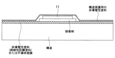
航空機31の外表面には、まず、非導電性塗料(絶縁性防錆塗料など)または不導体被膜が施されて外表面に対する絶縁領域が下地(非導電性の層)として構成される。そして、この絶縁領域上に回路11が形成され、RFIDタグ12が設置される。回路11は、航空機31の外表面に密着される。このため、航空機31の外表面から外部へ向けて非導電性の層、回路11及びRFIDタグ12の層、非導電性の大気の順に積層された構造となる。すなわち、回路11は、電気的には非導電性の部材で絶縁された状態となる。回路11及びRFIDタグ12の層、および非導電性の各層は薄膜形状で構成されるため、航空機31の外表面に対して大きな凹凸を発生させることなくシステムが構成される。
図8は、本開示の一実施形態に係る回路のA-A断面図である。図8で示される回路11は、非導電性塗料または不導体被膜による非導電性の層の上(外側、航空機31の構造の外側)に導電性塗料または導電性粉末により形成されている。
図9は、本開示の一実施形態に係る回路のA-A断面図である。図9で示される回路11は、金属薄膜または小径金属ワイヤにより形成されている。回路11は、非導電性塗料または不導体被膜による非導電性の層の上に塗布された接着剤により、固定されている。
また、回路11及びRFIDタグ12の設置領域を含む所定領域とその他の領域とが連続した構造保護用の非導電性塗料で覆われてもよい。
図10は、本開示の一実施形態に係る回路のA-A断面図である。図10で示される回路11は、非導電性塗料または不導体被膜による非導電性の層の上(外側、航空機31の構造の外側)に導電性塗料または導電性粉末により形成されている。回路11は、その全体が構造保護用の非導電性塗料で覆われる。
図11は、本開示の一実施形態に係る回路のA-A断面図である。図11で示される回路11は、金属薄膜または小径金属ワイヤにより形成されている。回路11は、非導電性塗料または不導体被膜による非導電性の層の上に塗布された接着剤により、固定されている。回路11は、その全体が構造保護用の非導電性塗料で覆われる。
回路11を構造保護用の非導電性塗料で覆うことにより、経済的価値のある外観を保ちながら、表面の段差を抑制して平滑化することができる。このため、空気抵抗の影響に敏感な移動体(例えば高速移動体)や、外観の重要な移動体(例えばスポーツカー)に対して適用することができる。
また、回路11及びRFIDタグ12の設置領域を含む所定領域とその他の領域とが連続した保温用の非導電性断熱材で覆われてもよい。移動体内部の熱環境を保ちながら、表面の段差を抑制して平滑化することができる。このため、空気抵抗の影響に敏感な移動体(例えばロケットや水素航空機)に対して適用可能である。 Next, the configuration of the outer surface of theaircraft 31 will be described.
First, the outer surface of theaircraft 31 is coated with a non-conductive paint (such as an insulating rust-preventive paint) or a non-conductive coating to form an insulating region for the outer surface as a base (non-conductive layer). Then, a circuit 11 is formed on this insulating area and an RFID tag 12 is installed. Circuit 11 is adhered to the outer surface of aircraft 31 . Therefore, a non-conductive layer, a layer of the circuit 11 and the RFID tag 12, and a non-conductive atmosphere are laminated in this order from the outer surface of the aircraft 31 toward the outside. That is, the circuit 11 is electrically insulated by a non-conductive member. Since the layers of the circuit 11 and the RFID tag 12 and the non-conductive layers are formed in the form of thin films, the system is constructed without causing large irregularities on the outer surface of the aircraft 31 .
FIG. 8 is a cross-sectional view AA of a circuit according to one embodiment of the present disclosure. Thecircuit 11 shown in FIG. 8 is formed by a conductive paint or conductive powder on top of a non-conductive layer (outside, outside the structure of the aircraft 31) of non-conductive paint or coating.
FIG. 9 is a cross-section AA of a circuit according to one embodiment of the present disclosure. Thecircuit 11 shown in FIG. 9 is formed of a metal thin film or a small-diameter metal wire. Circuit 11 is secured by an adhesive applied over a non-conductive layer of non-conductive paint or coating.
Further, a predetermined area including the installation area of thecircuit 11 and the RFID tag 12 and other areas may be continuously covered with a non-conductive paint for structural protection.
FIG. 10 is a cross-sectional view AA of a circuit according to one embodiment of the present disclosure. Thecircuit 11 shown in FIG. 10 is formed by a conductive paint or powder on top of a non-conductive layer (outside, outside the structure of the aircraft 31) of non-conductive paint or coating. The entire circuit 11 is covered with non-conductive paint for structural protection.
FIG. 11 is a cross-sectional view AA of a circuit according to one embodiment of the present disclosure. Thecircuit 11 shown in FIG. 11 is formed by a metal thin film or a small-diameter metal wire. Circuit 11 is secured by an adhesive applied over a non-conductive layer of non-conductive paint or coating. The entire circuit 11 is covered with non-conductive paint for structural protection.
By covering thecircuit 11 with a non-conductive paint for structural protection, the surface can be smoothed by suppressing steps while maintaining an economically valuable appearance. Therefore, it can be applied to moving objects sensitive to the influence of air resistance (for example, high-speed moving objects) and to moving objects whose appearance is important (for example, sports cars).
Further, a predetermined area including the installation area of thecircuit 11 and the RFID tag 12 and other areas may be covered with a continuous non-conductive heat insulating material for heat retention. While maintaining the thermal environment inside the moving body, the surface can be smoothed by suppressing steps. Therefore, it can be applied to mobile objects (such as rockets and hydrogen aircraft) that are sensitive to the effects of air resistance.
航空機31の外表面には、まず、非導電性塗料(絶縁性防錆塗料など)または不導体被膜が施されて外表面に対する絶縁領域が下地(非導電性の層)として構成される。そして、この絶縁領域上に回路11が形成され、RFIDタグ12が設置される。回路11は、航空機31の外表面に密着される。このため、航空機31の外表面から外部へ向けて非導電性の層、回路11及びRFIDタグ12の層、非導電性の大気の順に積層された構造となる。すなわち、回路11は、電気的には非導電性の部材で絶縁された状態となる。回路11及びRFIDタグ12の層、および非導電性の各層は薄膜形状で構成されるため、航空機31の外表面に対して大きな凹凸を発生させることなくシステムが構成される。
図8は、本開示の一実施形態に係る回路のA-A断面図である。図8で示される回路11は、非導電性塗料または不導体被膜による非導電性の層の上(外側、航空機31の構造の外側)に導電性塗料または導電性粉末により形成されている。
図9は、本開示の一実施形態に係る回路のA-A断面図である。図9で示される回路11は、金属薄膜または小径金属ワイヤにより形成されている。回路11は、非導電性塗料または不導体被膜による非導電性の層の上に塗布された接着剤により、固定されている。
また、回路11及びRFIDタグ12の設置領域を含む所定領域とその他の領域とが連続した構造保護用の非導電性塗料で覆われてもよい。
図10は、本開示の一実施形態に係る回路のA-A断面図である。図10で示される回路11は、非導電性塗料または不導体被膜による非導電性の層の上(外側、航空機31の構造の外側)に導電性塗料または導電性粉末により形成されている。回路11は、その全体が構造保護用の非導電性塗料で覆われる。
図11は、本開示の一実施形態に係る回路のA-A断面図である。図11で示される回路11は、金属薄膜または小径金属ワイヤにより形成されている。回路11は、非導電性塗料または不導体被膜による非導電性の層の上に塗布された接着剤により、固定されている。回路11は、その全体が構造保護用の非導電性塗料で覆われる。
回路11を構造保護用の非導電性塗料で覆うことにより、経済的価値のある外観を保ちながら、表面の段差を抑制して平滑化することができる。このため、空気抵抗の影響に敏感な移動体(例えば高速移動体)や、外観の重要な移動体(例えばスポーツカー)に対して適用することができる。
また、回路11及びRFIDタグ12の設置領域を含む所定領域とその他の領域とが連続した保温用の非導電性断熱材で覆われてもよい。移動体内部の熱環境を保ちながら、表面の段差を抑制して平滑化することができる。このため、空気抵抗の影響に敏感な移動体(例えばロケットや水素航空機)に対して適用可能である。 Next, the configuration of the outer surface of the
First, the outer surface of the
FIG. 8 is a cross-sectional view AA of a circuit according to one embodiment of the present disclosure. The
FIG. 9 is a cross-section AA of a circuit according to one embodiment of the present disclosure. The
Further, a predetermined area including the installation area of the
FIG. 10 is a cross-sectional view AA of a circuit according to one embodiment of the present disclosure. The
FIG. 11 is a cross-sectional view AA of a circuit according to one embodiment of the present disclosure. The
By covering the
Further, a predetermined area including the installation area of the
構造保護用の非導電性塗料として、例えばポリウレタンエナメルやエポキシプライマが挙げられるが、これに限られるものではない。
Non-conductive paints for structural protection include, but are not limited to, polyurethane enamels and epoxy primers.
保温用の非導電性断熱材として、例えば発泡ウレタン断熱材やグラスウールが挙げられるが、これに限られるものではない。
Examples of non-conductive heat insulating materials for heat retention include urethane foam heat insulating materials and glass wool, but are not limited to these.
RFIDタグ12が設置された位置については、構造保護用の非導電性塗料で覆われたあとに、目印をつけ、外部から認識できるようにすることが好ましい。また、予めRFIDタグ12の設置位置とRFIDタグ12のRFIDICチップ14内の固有識別情報とを組み合わせて記録しておくことが好ましい。
It is preferable to mark the position where the RFID tag 12 is installed after covering it with a non-conductive paint for structural protection so that it can be recognized from the outside. Moreover, it is preferable to record in advance a combination of the installation position of the RFID tag 12 and the unique identification information in the RFID chip 14 of the RFID tag 12 .
次に、回路11の具体的な設置箇所について説明する。
検査システム10は、航空機31の外表面の損傷を検出するものであるため、回路11は損傷が発生しやすいと想定される箇所に配置されることが好ましい。損傷が発生しやすい場所とは、例えば、カットアウト位置(部材の端部)や高い応力が発生する箇所(応力集中が発生しやすい箇所)である。すなわち、カットアウト位置や応力集中箇所の周辺に回路11を設けることが好ましい。 Next, specific installation locations of thecircuit 11 will be described.
Since theinspection system 10 detects damage to the outer surface of the aircraft 31, the circuit 11 is preferably located where damage is expected to occur. The places where damage is likely to occur are, for example, cutout positions (ends of members) and places where high stress occurs (places where stress concentration tends to occur). In other words, it is preferable to provide the circuit 11 around the cutout position and the stress concentrated portion.
検査システム10は、航空機31の外表面の損傷を検出するものであるため、回路11は損傷が発生しやすいと想定される箇所に配置されることが好ましい。損傷が発生しやすい場所とは、例えば、カットアウト位置(部材の端部)や高い応力が発生する箇所(応力集中が発生しやすい箇所)である。すなわち、カットアウト位置や応力集中箇所の周辺に回路11を設けることが好ましい。 Next, specific installation locations of the
Since the
図4は、航空機31に対して回路11を設置した場合の例を示す図である。図4は、航空機構造のカットアウト位置周辺に回路11を設けた場合の例を示している。図4に示すように、回路11は、航空機31の窓(例えば客室窓)21、航空機31のコックピット風防24、扉(ドア)25、扉(非常脱出口)26、外表面におけるアンテナの取り付け箇所27を囲うように設けられる。また、外表面のファスナ締結部(ファスナ部)28の近傍(亀裂進展が予想される範囲)を通過するように回路11を設けても良い。ファスナ締結部28とは、航空機31を構成する部材と部材との接手部であり、特に部材に開けた開口部周辺とそこに差し込むファスナ22を備えた部分を指す。
FIG. 4 is a diagram showing an example when the circuit 11 is installed on the aircraft 31. As shown in FIG. FIG. 4 shows an example of a circuit 11 provided around a cut-out location in the aircraft structure. As shown in FIG. 4, the circuit 11 includes a window (for example, a cabin window) 21 of an aircraft 31, a cockpit windshield 24 of the aircraft 31, a door (door) 25, a door (emergency exit) 26, and an antenna attachment point on an outer surface. 27. Alternatively, the circuit 11 may be provided so as to pass through the vicinity of the fastener fastening portion (fastener portion) 28 on the outer surface (the range where the crack is expected to grow). The fastener fastening portion 28 is a joint portion between members constituting the aircraft 31, and particularly refers to a portion around an opening opened in the member and a portion provided with the fastener 22 to be inserted therein.
図5は、航空機31に対して回路11を設置した場合の例を示す図である。図5は、航空機31を下から見た図である。図5は、航空機構造の応力集中箇所周辺に回路11を設けた場合の例を示している。図5に示すように、回路11は、マンホール41を囲うように設けられる。また、回路11は、翼胴の結合部42、着陸装置の取り付け部43、及び金具取り付け部44のそれぞれに対して、近傍(亀裂進展が予想される範囲)を通過するように設けられる。マンホール41とは、内部へアクセスするための口であり蓋で閉じられている。金具は、航空機31に取り付けれた金具である。例えば、近傍は、回路11を設ける対象の部の端(または接手部)から2.5cmの範囲である。
FIG. 5 is a diagram showing an example in which the circuit 11 is installed on the aircraft 31. As shown in FIG. FIG. 5 is a view of the aircraft 31 viewed from below. FIG. 5 shows an example in which a circuit 11 is provided around a stress concentration point in an aircraft structure. As shown in FIG. 5, the circuit 11 is provided so as to surround the manhole 41 . In addition, the circuit 11 is provided so as to pass through the vicinity (range where crack growth is expected) of each of the connecting portion 42 of the wing body, the mounting portion 43 of the landing gear, and the fitting portion 44 . The manhole 41 is an opening for accessing the inside and is closed with a lid. The metal fittings are metal fittings attached to the aircraft 31 . For example, the neighborhood is a range of 2.5 cm from the end (or joint) of the part where the circuit 11 is provided.
図6は、クラックの例を示している。図6のように損傷が発生すると、この損傷に伴って回路11が断線して、RFIDタグ12によって検出される。
Fig. 6 shows an example of cracks. When damage occurs as shown in FIG. 6, the circuit 11 is disconnected due to the damage and detected by the RFID tag 12 .
なお、図4から図5で例示した回路11の設置箇所は、同様の構成があれば航空機31に限定されず他の移動体に適用することとしてもよい。また、回路11の設置位置は、外表面に限定されず、移動体構造の内部に設けられることとしてもよい。
It should be noted that the installation location of the circuit 11 illustrated in FIGS. 4 and 5 is not limited to the aircraft 31 and may be applied to other moving bodies as long as they have the same configuration. Also, the position where the circuit 11 is installed is not limited to the outer surface, and it may be installed inside the mobile structure.
以上説明したように、本実施形態に係る検査システムによれば、移動体の外表面に導電性塗料、導電性粉末、金属薄膜または小径金属ワイヤにより構成された導電性の回路11と、RFIDタグ12のRFIDICチップ14とで閉回路が構成される。このため、RFIDタグ12のRFIDICチップ14により回路11の導通状態(電流値や抵抗値等)を検出することで、移動体の外表面の亀裂等の状態を検出することができる。一度に複数のRFIDタグ12で状態読み取りが高速でできるため、検査を効率化することができる。点検頻度を増加することが可能となり、安全性向上が期待できる。
またセンサ端子16とRFアンテナ15とRFIDICチップ14を不導体台座17が保持するため、金属やCFRPなどの電波を通さない検査対象であっても、RFIDリーダ13とRFIDICチップ14を用いた遠隔検査が可能となる。 As described above, according to the inspection system according to the present embodiment, theconductive circuit 11 made of conductive paint, conductive powder, metal thin film or small-diameter metal wire, and the RFID tag are formed on the outer surface of the moving object. 12 RFID chips 14 form a closed circuit. Therefore, by detecting the conduction state (current value, resistance value, etc.) of the circuit 11 with the RFID chip 14 of the RFID tag 12, it is possible to detect a state such as a crack on the outer surface of the moving body. Since the status of a plurality of RFID tags 12 can be read at high speed at once, inspection can be made more efficient. It is possible to increase the frequency of inspections, and an improvement in safety can be expected.
In addition, since thesensor terminal 16, the RF antenna 15, and the RFID chip 14 are held by the non-conductor base 17, remote inspection using the RFID reader 13 and the RFID chip 14 is possible even for objects such as metal and CFRP that do not transmit radio waves. becomes possible.
またセンサ端子16とRFアンテナ15とRFIDICチップ14を不導体台座17が保持するため、金属やCFRPなどの電波を通さない検査対象であっても、RFIDリーダ13とRFIDICチップ14を用いた遠隔検査が可能となる。 As described above, according to the inspection system according to the present embodiment, the
In addition, since the
導電性塗料、導電性粉末、金属薄膜または小径金属ワイヤで構成された回路11とRFIDタグ12とを用いることで、移動体の外表面の出っ張りを最小化して移動体の空気抵抗の増加を抑えることができる。
By using a circuit 11 made of conductive paint, conductive powder, a metal thin film, or a small-diameter metal wire and an RFID tag 12, protrusions on the outer surface of the moving body are minimized to suppress an increase in air resistance of the moving body. be able to.
導電性塗料、導電性粉末、金属薄膜または小径金属ワイヤにより回路11が構成されることで、移動体の外表面に従って回路11が切断される。一方で、移動体の外表面の歪み等の軽度な変形に対しては、材料の弾性によって回路11の導通状態が維持され、損傷の誤検知を抑制する。
The circuit 11 is cut along the outer surface of the moving body by forming the circuit 11 with conductive paint, conductive powder, metal thin film, or small-diameter metal wire. On the other hand, with respect to slight deformation such as distortion of the outer surface of the moving body, the elasticity of the material maintains the conductive state of the circuit 11, thereby suppressing erroneous detection of damage.
回路11と、RFIDタグ12と、移動体の外表面における回路11及びRFIDタグ12の周りの所定領域とその他の領域とが連続した非導電性塗料または非導電性断熱材などの外装材で覆われているため、表面の段差を抑制して平滑化することができる。また、外観や断熱等の経済性や機能性を損ねることなく両立が可能である。
The circuit 11, the RFID tag 12, and a predetermined area around the circuit 11 and the RFID tag 12 on the outer surface of the moving body and other areas are continuously covered with an exterior material such as non-conductive paint or non-conductive heat insulating material. Therefore, it is possible to suppress steps on the surface and smooth the surface. In addition, both are possible without impairing economic efficiency and functionality such as appearance and heat insulation.
本開示は、上述の実施形態のみに限定されるものではなく、発明の要旨を逸脱しない範囲において、種々変形実施が可能である。
The present disclosure is not limited to the above-described embodiments, and various modifications can be made without departing from the scope of the invention.
以上説明した各実施形態に記載の検査システムは例えば以下のように把握される。
本開示に係る検査システム(10)は、移動体(31)に適用される検査システムであって、前記移動体の構造表面の絶縁性塗料上または不導体被膜上に設けられ、該絶縁性塗料または該不導体被膜と密着した導電性回路(11)と、前記導電性回路に接続されるセンサ端子(16)と、RFアンテナ(15)に接続されるRFアンテナ端子とを備え、前記導電性回路の導通状態を検出するRFIDICチップ(14)と、前記センサ端子と前記RFアンテナと前記RFIDICチップを適切な位置に保持する不導体台座(17)と、を備える。 For example, the inspection system described in each embodiment described above is grasped as follows.
An inspection system (10) according to the present disclosure is an inspection system applied to a moving body (31), and is provided on an insulating coating or a non-conductive coating on the structural surface of the moving body, and the insulating coating Alternatively, the conductive It comprises an RFID chip (14) for detecting continuity of a circuit, and a non-conductive base (17) for holding said sensor terminals, said RF antenna and said RFID chip in proper positions.
本開示に係る検査システムは、移動体の構造表面の絶縁性塗料上または不導体被膜上に設けられ、絶縁性塗料または不導体被膜と密着した導電性回路と、導電性回路に接続されるセンサ端子と、RFアンテナに接続されるRFアンテナ端子とを備え、導電性回路の導通状態を検出するRFIDICチップとで構成される。このため、RFIDICチップにより導電性回路の導通状態(切断や抵抗等)を検出することで、移動体表面の亀裂等の状態を検出することができる。RFIDICチップで状態読み取りができるため、検査を効率化することができる。点検頻度を増加することが可能となり、安全性向上が期待できる。
またセンサ端子とRFアンテナとRFIDICチップを不導体台座が保持するため、金属やCFRPなどの電波を通さない検査対象であっても、RFIDリーダとRFIDICチップを用いた遠隔検査が可能となる。 An inspection system according to the present disclosure includes a conductive circuit provided on an insulating paint or a non-conductive film on a structural surface of a moving body and in close contact with the insulating paint or the non-conductive film; and a sensor connected to the conductive circuit. and an RF antenna terminal connected to an RF antenna, and an RFID IC chip for detecting the conduction state of a conductive circuit. Therefore, by detecting the conduction state (disconnection, resistance, etc.) of the conductive circuit with the RFID chip, it is possible to detect the state of cracks on the surface of the moving body. Since the status can be read by the RFID chip, inspection can be made more efficient. It is possible to increase the frequency of inspections, and an improvement in safety can be expected.
In addition, since the non-conductive pedestal holds the sensor terminal, the RF antenna and the RFID chip, remote inspection using the RFID reader and the RFID chip is possible even for an object to be inspected, such as metal or CFRP, which does not transmit radio waves.
移動体の構造表面の絶縁性塗料上または不導体被膜上に設けられ、絶縁性塗料または不導体被膜と密着した導電性回路とRFIDICチップとを用いることで、移動体表面の段差を抑制して移動体の空気抵抗の増加を抑えることができる。
By using the conductive circuit and the RFID chip provided on the insulating paint or the non-conductive film on the structural surface of the moving object and in close contact with the insulating paint or the non-conductive film, the step on the surface of the moving object is suppressed. It is possible to suppress an increase in air resistance of the moving body.
絶縁性塗料または不導体被膜により導電性回路が構成されることで、移動体表面に従って回路が切断される。一方で、移動体表面の歪み等の軽度な変形に対しては、材料の弾性によって回路状態が維持され、誤検知を抑制する。
By forming a conductive circuit with insulating paint or non-conductive coating, the circuit is cut along the surface of the moving object. On the other hand, with respect to slight deformation such as distortion of the surface of the moving body, the elasticity of the material maintains the circuit state and suppresses erroneous detection.
本開示に係る検査システムにおいて、絶縁性塗料または不導体被膜は、移動体に密着する界面強度を有するとしてもよい。
In the inspection system according to the present disclosure, the insulating paint or non-conductive coating may have interfacial strength to adhere to the moving object.
本開示に係る検査システムによれば、絶縁性塗料または不導体被膜が移動体に密着する界面強度を有することで、絶縁性塗料または不導体被膜は移動体の構造を腐食や外傷から保護する層を構成することができる。
According to the inspection system according to the present disclosure, the insulating paint or non-conductive coating has an interfacial strength such that the insulating paint or non-conductive coating adheres to the moving body, so that the insulating coating or non-conductive coating is a layer that protects the structure of the moving body from corrosion and external damage. can be configured.
本開示に係る検査システムにおいて、導電性回路は、導電性分子または導電性単体原子を溶質とし、硬化時に絶縁性塗料または不導体被膜に密着する有機化合物溶媒である導電性塗料により形成されることとしてもよい。
In the inspection system according to the present disclosure, the conductive circuit is formed by a conductive paint that is an organic compound solvent that uses conductive molecules or conductive single atoms as a solute and adheres to the insulating paint or non-conductive film when cured. may be
本開示に係る検査システムによれば、導電性回路が導電性分子または導電性単体原子を溶質とし、硬化時に絶縁性塗料または不導体被膜に密着する有機化合物溶媒である導電性塗料により形成されることで、導電性に加え、硬化時における密着性を有する回路が構成される。
According to the inspection system according to the present disclosure, the conductive circuit is formed by a conductive paint that is an organic compound solvent that uses conductive molecules or conductive single atoms as a solute and adheres to the insulating paint or non-conductive film when cured. As a result, a circuit having adhesion at the time of curing is formed in addition to conductivity.
本開示に係る検査システムにおいて、導電性回路は、絶縁性塗料または不導体被膜に付着可能であり、導電性分子または導電性単体原子が組成の50%以上を占める導電性粉末により形成されることとしてもよい。
In the inspection system according to the present disclosure, the conductive circuit can be attached to an insulating paint or a non-conductive coating, and is formed of a conductive powder in which conductive molecules or conductive single atoms account for 50% or more of the composition. may be
本開示に係る検査システムによれば、導電性回路が絶縁性塗料または不導体被膜に付着可能であり、導電性分子または導電性単体原子が組成の50%以上を占める導電性粉末により形成されることで、導電性に加え形成時に付着できる特性を有する回路が構成される。
According to the inspection system according to the present disclosure, a conductive circuit can be attached to an insulating paint or a non-conductive coating, and is formed of a conductive powder in which conductive molecules or conductive single atoms account for 50% or more of the composition. This creates a circuit that has the property of being adherent as it is formed, in addition to being conductive.
本開示に係る検査システムにおいて、導電性回路は、絶縁性塗料または不導体被膜に接着剤を介して接合される厚さ70μm以下の金属薄膜または直径200μm以下の金属ワイヤにより形成されることとしてもよい。
In the inspection system according to the present disclosure, the conductive circuit is formed by a metal thin film with a thickness of 70 μm or less or a metal wire with a diameter of 200 μm or less bonded to an insulating paint or non-conductive coating via an adhesive. good.
本開示に係る検査システムによれば、導電性回路は、絶縁性塗料または不導体被膜に接着剤を介して接合される厚さ70μm以下の金属薄膜または直径200μm以下の金属ワイヤにより形成されることで、接着剤の界面強度の方が勝るように、金属薄膜または金属ワイヤの寸法を一定以下にコントロールし、損傷時の検知を確実なものとすることができる。
According to the inspection system according to the present disclosure, the conductive circuit is formed by a metal thin film with a thickness of 70 μm or less or a metal wire with a diameter of 200 μm or less bonded to an insulating paint or non-conductive coating via an adhesive. Therefore, it is possible to control the dimension of the metal thin film or metal wire to a certain level or less so that the interface strength of the adhesive is superior, and to ensure the detection of damage.
本開示に係る検査システムにおいて、RFIDICチップは、RFアンテナを介して無線で電力の受電および信号送受信を行い、導電性回路に切断が生じているか否かを検出することとしてもよい。
In the inspection system according to the present disclosure, the RFID chip may receive power and transmit and receive signals wirelessly via an RF antenna to detect whether or not a conductive circuit is disconnected.
本開示に係る検査システムによれば、RFIDICチップで回路に切断が生じているか否かを検出することで、移動体の表面の亀裂を検出することができる。
According to the inspection system according to the present disclosure, it is possible to detect cracks on the surface of the mobile object by detecting whether or not the RFID chip has caused a circuit breakage.
本開示に係る検査システムにおいて、導電性回路およびRFIDICチップの設置領域を含む所定領域とその他の領域とが、非導電性材料で覆われていることとしてもよい。
In the inspection system according to the present disclosure, the predetermined area including the installation area of the conductive circuit and the RFID chip and other areas may be covered with a non-conductive material.
本開示に係る検査システムによれば、導電性回路およびRFIDICチップの設置領域を含む所定領域とその他の領域とが非導電性材料で覆われているため、移動体表面の段差を抑制して平滑化することができる。
According to the inspection system according to the present disclosure, since the predetermined area including the installation area of the conductive circuit and the RFID chip and other areas are covered with the non-conductive material, the surface of the moving object is smoothed by suppressing steps. can be
本開示に係る検査システムは、RFアンテナを介してRFIDICチップへの電力供給、および情報の送受信を行うRFIDリーダ(13)を備えることとしてもよい。
The inspection system according to the present disclosure may include an RFID reader (13) that supplies power to the RFID chip and transmits and receives information via an RF antenna.
本開示に係る検査システムによれば、RFIDリーダによりRFIDICチップで検出した導電性回路の導通状態を読み取ることができる。
According to the inspection system according to the present disclosure, the RFID reader can read the conduction state of the conductive circuit detected by the RFID chip.
本開示に係る検査システムは、RFアンテナ及びRFIDICチップを保持する不導体台座を備えることとしてもよい。本開示に係る検査システムによれば、RFアンテナと検査対象である構造との間に適切な寸法の不導体台座を適用するため、金属やCFRP等の電波を通さない検査対象でも、RFIDリーダとRFIDICチップを利用した遠隔検査が可能となり、RFリーダからの電力受電および信号送受信能力を向上させることができる。
The inspection system according to the present disclosure may include a non-conductive pedestal that holds the RF antenna and the RFID chip. According to the inspection system according to the present disclosure, since a non-conductive pedestal with appropriate dimensions is applied between the RF antenna and the structure to be inspected, even an inspection object such as metal or CFRP that does not transmit radio waves can be used as an RFID reader. Remote inspection using the RFID chip becomes possible, and power reception and signal transmission/reception capability from the RF reader can be improved.
10 :検査システム
11 :回路(導電性回路)
12 :RFIDタグ
13 :RFIDリーダ
14 :RFIDICチップ
15 :RFIDアンテナ
20 :胴体外板
21 :窓
22 :ファスナ
23 :箇所
24 :コックピット風防
27 :取り付け箇所
31 :航空機
41 :マンホール
42 :結合部
43 :取り付け部
44 :金具取り付け部
10: inspection system 11: circuit (conductive circuit)
12: RFID tag 13: RFID reader 14: RFID chip 15: RFID antenna 20: fuselage outer plate 21: window 22: fastener 23: location 24: cockpit windshield 27: attachment location 31: aircraft 41: manhole 42: joint 43: Mounting portion 44: Metal fitting mounting portion
Claims (9)
- 移動体に適用される検査システムであって、
前記移動体の構造表面の絶縁性塗料上または不導体被膜上に設けられ、該絶縁性塗料または該不導体被膜と密着した導電性回路と、
前記導電性回路に接続されるセンサ端子と、RFアンテナに接続されるRFアンテナ端子とを備え、前記導電性回路の導通状態を検出するRFIDICチップと、
を備える検査システム。 An inspection system applied to a moving body,
a conductive circuit provided on the insulating paint or the non-conductive coating on the structural surface of the moving body and in close contact with the insulating paint or the non-conductive coating;
an RFID IC chip, comprising a sensor terminal connected to the conductive circuit and an RF antenna terminal connected to an RF antenna, for detecting the conduction state of the conductive circuit;
inspection system. - 前記絶縁性塗料または前記不導体被膜は、前記移動体に密着する界面強度を有する請求項1に記載の検査システム。 The inspection system according to claim 1, wherein the insulating paint or the non-conductive coating has interface strength to adhere to the moving body.
- 前記導電性回路は、導電性分子または導電性単体原子を溶質とし、硬化時に前記絶縁性塗料または前記不導体被膜に密着する有機化合物溶媒である導電性塗料により形成される請求項1に記載の検査システム。 2. The conductive circuit according to claim 1, wherein the conductive circuit is formed of a conductive paint that is an organic compound solvent that uses conductive molecules or conductive single atoms as a solute and adheres to the insulating paint or the nonconductive film when cured. inspection system.
- 前記導電性回路は、前記絶縁性塗料または前記不導体被膜に付着可能であり、導電性分子または導電性単体原子が組成の50%以上を占める導電性粉末により形成される請求項1に記載の検査システム。 2. The conductive circuit according to claim 1, wherein the conductive circuit can be adhered to the insulating paint or the nonconductive coating, and is formed of a conductive powder in which conductive molecules or conductive single atoms account for 50% or more of the composition. inspection system.
- 前記導電性回路は、前記絶縁性塗料または前記不導体被膜に接着剤を介して接合される厚さ70μm以下の金属薄膜または直径200μm以下の金属ワイヤにより形成される請求項1に記載の検査システム。 2. The inspection system according to claim 1, wherein the conductive circuit is formed of a metal thin film having a thickness of 70 μm or less or a metal wire having a diameter of 200 μm or less bonded to the insulating paint or the non-conductive coating via an adhesive. .
- 前記RFIDICチップは、前記RFアンテナを介して無線で電力の受電および信号送受信を行い、前記導電性回路に切断が生じているか否かを検出する請求項1から請求項5のいずれか1項に記載の検査システム。 6. The RFID chip according to any one of claims 1 to 5, wherein the RFID chip wirelessly receives power and transmits and receives signals via the RF antenna, and detects whether or not the conductive circuit is disconnected. Inspection system as described.
- 前記導電性回路および前記RFIDICチップの設置領域を含む所定領域とその他の領域とが、非導電性材料で覆われている請求項1から請求項5のいずれか1項に記載の検査システム。 The inspection system according to any one of claims 1 to 5, wherein a predetermined area including an installation area of the conductive circuit and the RFID chip and other areas are covered with a non-conductive material.
- 前記RFアンテナを介して前記RFIDICチップへの電力供給、および情報の送受信を行うRFIDリーダを備える請求項1から請求項5のいずれか1項に記載の検査システム。 The inspection system according to any one of claims 1 to 5, comprising an RFID reader that supplies power to the RFID chip via the RF antenna and transmits and receives information.
- 前記RFアンテナ及び前記RFIDICチップを保持する不導体台座を備える請求項1から請求項5のいずれか1項に記載の検査システム。
6. The inspection system of any one of claims 1-5, comprising a non-conductive pedestal that holds the RF antenna and the RFID chip.
Priority Applications (1)
| Application Number | Priority Date | Filing Date | Title |
|---|---|---|---|
| JP2023542379A JPWO2023022098A1 (en) | 2021-08-17 | 2022-08-10 |
Applications Claiming Priority (4)
| Application Number | Priority Date | Filing Date | Title |
|---|---|---|---|
| JP2021-132689 | 2021-08-17 | ||
| JP2021132689 | 2021-08-17 | ||
| JP2022086029 | 2022-05-26 | ||
| JP2022-086029 | 2022-05-26 |
Publications (1)
| Publication Number | Publication Date |
|---|---|
| WO2023022098A1 true WO2023022098A1 (en) | 2023-02-23 |
Family
ID=85240698
Family Applications (1)
| Application Number | Title | Priority Date | Filing Date |
|---|---|---|---|
| PCT/JP2022/030662 WO2023022098A1 (en) | 2021-08-17 | 2022-08-10 | Inspection system |
Country Status (2)
| Country | Link |
|---|---|
| JP (1) | JPWO2023022098A1 (en) |
| WO (1) | WO2023022098A1 (en) |
Citations (7)
| Publication number | Priority date | Publication date | Assignee | Title |
|---|---|---|---|---|
| JPS6262252U (en) * | 1985-10-08 | 1987-04-17 | ||
| US5969260A (en) * | 1998-03-30 | 1999-10-19 | Mcdonnell Douglas Corporation | Remotely interrogatable apparatus and method for detecting defects in structural members |
| US20080223152A1 (en) * | 2005-12-14 | 2008-09-18 | The Boeing Company | Methods and systems for using active surface coverings for structural assessment and monitoring |
| US20110291802A1 (en) * | 2010-06-01 | 2011-12-01 | The Boeing Company | Structural health management device and associated system and method |
| JP2016040669A (en) * | 2014-08-12 | 2016-03-24 | 東芝テック株式会社 | Passive crack sensor |
| JP2016136127A (en) * | 2014-07-22 | 2016-07-28 | ザ・ボーイング・カンパニーThe Boeing Company | Blunt impact indicator methods |
| JP2020140605A (en) * | 2019-03-01 | 2020-09-03 | トッパン・フォームズ株式会社 | Crack detection label |
-
2022
- 2022-08-10 JP JP2023542379A patent/JPWO2023022098A1/ja active Pending
- 2022-08-10 WO PCT/JP2022/030662 patent/WO2023022098A1/en active Application Filing
Patent Citations (7)
| Publication number | Priority date | Publication date | Assignee | Title |
|---|---|---|---|---|
| JPS6262252U (en) * | 1985-10-08 | 1987-04-17 | ||
| US5969260A (en) * | 1998-03-30 | 1999-10-19 | Mcdonnell Douglas Corporation | Remotely interrogatable apparatus and method for detecting defects in structural members |
| US20080223152A1 (en) * | 2005-12-14 | 2008-09-18 | The Boeing Company | Methods and systems for using active surface coverings for structural assessment and monitoring |
| US20110291802A1 (en) * | 2010-06-01 | 2011-12-01 | The Boeing Company | Structural health management device and associated system and method |
| JP2016136127A (en) * | 2014-07-22 | 2016-07-28 | ザ・ボーイング・カンパニーThe Boeing Company | Blunt impact indicator methods |
| JP2016040669A (en) * | 2014-08-12 | 2016-03-24 | 東芝テック株式会社 | Passive crack sensor |
| JP2020140605A (en) * | 2019-03-01 | 2020-09-03 | トッパン・フォームズ株式会社 | Crack detection label |
Also Published As
| Publication number | Publication date |
|---|---|
| JPWO2023022098A1 (en) | 2023-02-23 |
Similar Documents
| Publication | Publication Date | Title |
|---|---|---|
| US9777838B2 (en) | Gasket seal, door of aircraft, seal structure for opening portion of aircraft, and aircraft | |
| US8998140B2 (en) | Window of aircraft, closing member for opening and gasket seal | |
| EP2479110B1 (en) | Lightning strike detection | |
| US8766511B2 (en) | Method and system for distributed network of nanoparticle ink based piezoelectric sensors for structural health monitoring | |
| EP1767344B1 (en) | Wide area lightning diverter overlay | |
| JP6664904B2 (en) | Conductive thermoplastic ground plane for use in aircraft | |
| CN105292470B (en) | A kind of electric power circuit detects without man-machine | |
| CN105292471B (en) | A kind of solar electric power wireline inspection unmanned plane | |
| KR20050070088A (en) | Sensors and systems for structural health monitoring | |
| WO2006086083A2 (en) | Method and system for lightning current conduction protection using foil bonded strips | |
| US10210740B2 (en) | System and method for monitoring structural health of bonded components | |
| US9065171B2 (en) | Antenna support bracket | |
| US4824713A (en) | Lightning protected structural surface | |
| WO2023022098A1 (en) | Inspection system | |
| WO2013105178A1 (en) | Aircraft window, aircraft, and assembly method for aircraft window | |
| WO2014184146A1 (en) | Anti-icing system | |
| JP2004323006A (en) | Lightning stroke reducing device and transportation device | |
| US20120218154A1 (en) | Slot antenna in a solar-reflective glazing | |
| CN112072335A (en) | Conductive structure between composite material structural members and conductive processing method | |
| CN109807037B (en) | Protection method for exposed electrode of optical shielding window | |
| CN112399916A (en) | Laminated glazing unit incorporating an antenna for an automatic landing assistance system | |
| CN114180083B (en) | Method for conducting electricity between composite structural members by using copper cups | |
| CN112510359A (en) | Invisible antenna housing |
Legal Events
| Date | Code | Title | Description |
|---|---|---|---|
| 121 | Ep: the epo has been informed by wipo that ep was designated in this application |
Ref document number: 22858419 Country of ref document: EP Kind code of ref document: A1 |
|
| WWE | Wipo information: entry into national phase |
Ref document number: 2023542379 Country of ref document: JP |
|
| NENP | Non-entry into the national phase |
Ref country code: DE |