WO2023008204A1 - Layered body manufacturing method, and kit for adhesive composition - Google Patents
Layered body manufacturing method, and kit for adhesive composition Download PDFInfo
- Publication number
- WO2023008204A1 WO2023008204A1 PCT/JP2022/027646 JP2022027646W WO2023008204A1 WO 2023008204 A1 WO2023008204 A1 WO 2023008204A1 JP 2022027646 W JP2022027646 W JP 2022027646W WO 2023008204 A1 WO2023008204 A1 WO 2023008204A1
- Authority
- WO
- WIPO (PCT)
- Prior art keywords
- adhesive composition
- adhesive
- units
- group
- thermosetting component
- Prior art date
Links
- 239000000853 adhesive Substances 0.000 title claims abstract description 258
- 230000001070 adhesive effect Effects 0.000 title claims abstract description 258
- 239000000203 mixture Substances 0.000 title claims abstract description 213
- 238000004519 manufacturing process Methods 0.000 title claims abstract description 45
- 239000000758 substrate Substances 0.000 claims abstract description 127
- 229920001187 thermosetting polymer Polymers 0.000 claims abstract description 113
- 239000011247 coating layer Substances 0.000 claims abstract description 89
- 239000004065 semiconductor Substances 0.000 claims abstract description 81
- 239000003054 catalyst Substances 0.000 claims abstract description 78
- 239000012790 adhesive layer Substances 0.000 claims abstract description 40
- 239000003795 chemical substances by application Substances 0.000 claims abstract description 35
- 238000000034 method Methods 0.000 claims description 33
- XUIMIQQOPSSXEZ-UHFFFAOYSA-N Silicon Chemical group [Si] XUIMIQQOPSSXEZ-UHFFFAOYSA-N 0.000 claims description 31
- 229910052710 silicon Inorganic materials 0.000 claims description 28
- 125000004432 carbon atom Chemical group C* 0.000 claims description 27
- BASFCYQUMIYNBI-UHFFFAOYSA-N platinum Chemical group [Pt] BASFCYQUMIYNBI-UHFFFAOYSA-N 0.000 claims description 21
- 125000003342 alkenyl group Chemical group 0.000 claims description 18
- 229910052751 metal Inorganic materials 0.000 claims description 9
- 239000002184 metal Substances 0.000 claims description 9
- 238000010438 heat treatment Methods 0.000 abstract description 23
- -1 siloxane unit Chemical group 0.000 description 119
- 239000010410 layer Substances 0.000 description 31
- 235000012431 wafers Nutrition 0.000 description 31
- 239000002904 solvent Substances 0.000 description 26
- 125000003700 epoxy group Chemical group 0.000 description 21
- 238000000576 coating method Methods 0.000 description 20
- 125000000217 alkyl group Chemical group 0.000 description 19
- 125000002496 methyl group Chemical group [H]C([H])([H])* 0.000 description 18
- 239000011248 coating agent Substances 0.000 description 16
- 239000010408 film Substances 0.000 description 16
- 238000004140 cleaning Methods 0.000 description 15
- 239000004205 dimethyl polysiloxane Substances 0.000 description 13
- 229920000435 poly(dimethylsiloxane) Polymers 0.000 description 13
- 150000003242 quaternary ammonium salts Chemical class 0.000 description 13
- 239000010703 silicon Substances 0.000 description 13
- 125000001997 phenyl group Chemical group [H]C1=C([H])C([H])=C(*)C([H])=C1[H] 0.000 description 12
- 239000000463 material Substances 0.000 description 11
- 238000005498 polishing Methods 0.000 description 9
- 229920004482 WACKER® Polymers 0.000 description 8
- 239000003599 detergent Substances 0.000 description 8
- 125000001495 ethyl group Chemical group [H]C([H])([H])C([H])([H])* 0.000 description 8
- 150000002430 hydrocarbons Chemical class 0.000 description 7
- 229910052697 platinum Inorganic materials 0.000 description 7
- 239000004215 Carbon black (E152) Substances 0.000 description 6
- 150000001408 amides Chemical class 0.000 description 6
- 229930195733 hydrocarbon Natural products 0.000 description 6
- 125000004435 hydrogen atom Chemical group [H]* 0.000 description 6
- FPGGTKZVZWFYPV-UHFFFAOYSA-M tetrabutylammonium fluoride Chemical compound [F-].CCCC[N+](CCCC)(CCCC)CCCC FPGGTKZVZWFYPV-UHFFFAOYSA-M 0.000 description 6
- 229920005992 thermoplastic resin Polymers 0.000 description 6
- 125000000391 vinyl group Chemical group [H]C([*])=C([H])[H] 0.000 description 6
- DDFHBQSCUXNBSA-UHFFFAOYSA-N 5-(5-carboxythiophen-2-yl)thiophene-2-carboxylic acid Chemical compound S1C(C(=O)O)=CC=C1C1=CC=C(C(O)=O)S1 DDFHBQSCUXNBSA-UHFFFAOYSA-N 0.000 description 5
- 229910004298 SiO 2 Inorganic materials 0.000 description 5
- 239000003960 organic solvent Substances 0.000 description 5
- 229920000642 polymer Polymers 0.000 description 5
- 238000002360 preparation method Methods 0.000 description 5
- SECXISVLQFMRJM-UHFFFAOYSA-N N-Methylpyrrolidone Chemical compound CN1CCCC1=O SECXISVLQFMRJM-UHFFFAOYSA-N 0.000 description 4
- PPBRXRYQALVLMV-UHFFFAOYSA-N Styrene Chemical compound C=CC1=CC=CC=C1 PPBRXRYQALVLMV-UHFFFAOYSA-N 0.000 description 4
- 125000002947 alkylene group Chemical group 0.000 description 4
- 150000001450 anions Chemical class 0.000 description 4
- 125000004122 cyclic group Chemical group 0.000 description 4
- KPUWHANPEXNPJT-UHFFFAOYSA-N disiloxane Chemical class [SiH3]O[SiH3] KPUWHANPEXNPJT-UHFFFAOYSA-N 0.000 description 4
- 230000000694 effects Effects 0.000 description 4
- 125000005843 halogen group Chemical group 0.000 description 4
- 125000001449 isopropyl group Chemical group [H]C([H])([H])C([H])(*)C([H])([H])[H] 0.000 description 4
- BKIMMITUMNQMOS-UHFFFAOYSA-N nonane Chemical compound CCCCCCCCC BKIMMITUMNQMOS-UHFFFAOYSA-N 0.000 description 4
- 239000000047 product Substances 0.000 description 4
- 229920005989 resin Polymers 0.000 description 4
- 239000011347 resin Substances 0.000 description 4
- 150000003839 salts Chemical class 0.000 description 4
- 238000004528 spin coating Methods 0.000 description 4
- 125000001424 substituent group Chemical group 0.000 description 4
- XLYOFNOQVPJJNP-UHFFFAOYSA-N water Substances O XLYOFNOQVPJJNP-UHFFFAOYSA-N 0.000 description 4
- VSKJLJHPAFKHBX-UHFFFAOYSA-N 2-methylbuta-1,3-diene;styrene Chemical compound CC(=C)C=C.C=CC1=CC=CC=C1.C=CC1=CC=CC=C1 VSKJLJHPAFKHBX-UHFFFAOYSA-N 0.000 description 3
- 239000004793 Polystyrene Substances 0.000 description 3
- YXFVVABEGXRONW-UHFFFAOYSA-N Toluene Chemical compound CC1=CC=CC=C1 YXFVVABEGXRONW-UHFFFAOYSA-N 0.000 description 3
- 239000002253 acid Substances 0.000 description 3
- 125000003277 amino group Chemical group 0.000 description 3
- 125000003118 aryl group Chemical group 0.000 description 3
- FACXGONDLDSNOE-UHFFFAOYSA-N buta-1,3-diene;styrene Chemical compound C=CC=C.C=CC1=CC=CC=C1.C=CC1=CC=CC=C1 FACXGONDLDSNOE-UHFFFAOYSA-N 0.000 description 3
- 125000003178 carboxy group Chemical group [H]OC(*)=O 0.000 description 3
- 239000002131 composite material Substances 0.000 description 3
- 229920001577 copolymer Polymers 0.000 description 3
- 125000004093 cyano group Chemical group *C#N 0.000 description 3
- 230000006866 deterioration Effects 0.000 description 3
- 239000006185 dispersion Substances 0.000 description 3
- 229920001971 elastomer Polymers 0.000 description 3
- 239000000806 elastomer Substances 0.000 description 3
- 229910052731 fluorine Inorganic materials 0.000 description 3
- 239000011737 fluorine Substances 0.000 description 3
- 125000001072 heteroaryl group Chemical group 0.000 description 3
- 238000006459 hydrosilylation reaction Methods 0.000 description 3
- 125000002887 hydroxy group Chemical group [H]O* 0.000 description 3
- 230000010354 integration Effects 0.000 description 3
- MBHINSULENHCMF-UHFFFAOYSA-N n,n-dimethylpropanamide Chemical compound CCC(=O)N(C)C MBHINSULENHCMF-UHFFFAOYSA-N 0.000 description 3
- VLKZOEOYAKHREP-UHFFFAOYSA-N n-Hexane Chemical compound CCCCCC VLKZOEOYAKHREP-UHFFFAOYSA-N 0.000 description 3
- 125000004108 n-butyl group Chemical group [H]C([H])([H])C([H])([H])C([H])([H])C([H])([H])* 0.000 description 3
- 125000000449 nitro group Chemical group [O-][N+](*)=O 0.000 description 3
- 125000000962 organic group Chemical group 0.000 description 3
- CFJYNSNXFXLKNS-UHFFFAOYSA-N p-menthane Chemical compound CC(C)C1CCC(C)CC1 CFJYNSNXFXLKNS-UHFFFAOYSA-N 0.000 description 3
- 229920002223 polystyrene Polymers 0.000 description 3
- 125000005372 silanol group Chemical group 0.000 description 3
- 229920006132 styrene block copolymer Polymers 0.000 description 3
- 229920000468 styrene butadiene styrene block copolymer Polymers 0.000 description 3
- ZFPGARUNNKGOBB-UHFFFAOYSA-N 1-Ethyl-2-pyrrolidinone Chemical compound CCN1CCCC1=O ZFPGARUNNKGOBB-UHFFFAOYSA-N 0.000 description 2
- UWNADWZGEHDQAB-UHFFFAOYSA-N 2,5-dimethylhexane Chemical group CC(C)CCC(C)C UWNADWZGEHDQAB-UHFFFAOYSA-N 0.000 description 2
- ZPVFWPFBNIEHGJ-UHFFFAOYSA-N 2-octanone Chemical compound CCCCCCC(C)=O ZPVFWPFBNIEHGJ-UHFFFAOYSA-N 0.000 description 2
- 125000003903 2-propenyl group Chemical group [H]C([*])([H])C([H])=C([H])[H] 0.000 description 2
- KRHYYFGTRYWZRS-UHFFFAOYSA-M Fluoride anion Chemical compound [F-] KRHYYFGTRYWZRS-UHFFFAOYSA-M 0.000 description 2
- YCKRFDGAMUMZLT-UHFFFAOYSA-N Fluorine atom Chemical compound [F] YCKRFDGAMUMZLT-UHFFFAOYSA-N 0.000 description 2
- NTIZESTWPVYFNL-UHFFFAOYSA-N Methyl isobutyl ketone Chemical compound CC(C)CC(C)=O NTIZESTWPVYFNL-UHFFFAOYSA-N 0.000 description 2
- UIHCLUNTQKBZGK-UHFFFAOYSA-N Methyl isobutyl ketone Natural products CCC(C)C(C)=O UIHCLUNTQKBZGK-UHFFFAOYSA-N 0.000 description 2
- IMNFDUFMRHMDMM-UHFFFAOYSA-N N-Heptane Chemical compound CCCCCCC IMNFDUFMRHMDMM-UHFFFAOYSA-N 0.000 description 2
- 229920000459 Nitrile rubber Polymers 0.000 description 2
- 239000004677 Nylon Substances 0.000 description 2
- VYPSYNLAJGMNEJ-UHFFFAOYSA-N Silicium dioxide Chemical compound O=[Si]=O VYPSYNLAJGMNEJ-UHFFFAOYSA-N 0.000 description 2
- WYURNTSHIVDZCO-UHFFFAOYSA-N Tetrahydrofuran Chemical compound C1CCOC1 WYURNTSHIVDZCO-UHFFFAOYSA-N 0.000 description 2
- 230000002411 adverse Effects 0.000 description 2
- 150000001336 alkenes Chemical class 0.000 description 2
- 125000000304 alkynyl group Chemical group 0.000 description 2
- 150000004945 aromatic hydrocarbons Chemical class 0.000 description 2
- 125000004429 atom Chemical group 0.000 description 2
- 230000000052 comparative effect Effects 0.000 description 2
- RWGFKTVRMDUZSP-UHFFFAOYSA-N cumene Chemical compound CC(C)C1=CC=CC=C1 RWGFKTVRMDUZSP-UHFFFAOYSA-N 0.000 description 2
- 125000001995 cyclobutyl group Chemical group [H]C1([H])C([H])([H])C([H])(*)C1([H])[H] 0.000 description 2
- 125000001559 cyclopropyl group Chemical group [H]C1([H])C([H])([H])C1([H])* 0.000 description 2
- DIOQZVSQGTUSAI-UHFFFAOYSA-N decane Chemical compound CCCCCCCCCC DIOQZVSQGTUSAI-UHFFFAOYSA-N 0.000 description 2
- SNRUBQQJIBEYMU-UHFFFAOYSA-N dodecane Chemical compound CCCCCCCCCCCC SNRUBQQJIBEYMU-UHFFFAOYSA-N 0.000 description 2
- 229920006228 ethylene acrylate copolymer Polymers 0.000 description 2
- 239000011521 glass Substances 0.000 description 2
- 229910052736 halogen Inorganic materials 0.000 description 2
- 125000000959 isobutyl group Chemical group [H]C([H])([H])C([H])(C([H])([H])[H])C([H])([H])* 0.000 description 2
- 150000002576 ketones Chemical class 0.000 description 2
- XMGQYMWWDOXHJM-UHFFFAOYSA-N limonene Chemical compound CC(=C)C1CCC(C)=CC1 XMGQYMWWDOXHJM-UHFFFAOYSA-N 0.000 description 2
- 238000002844 melting Methods 0.000 description 2
- 239000012528 membrane Substances 0.000 description 2
- GXMIHVHJTLPVKL-UHFFFAOYSA-N n,n,2-trimethylpropanamide Chemical compound CC(C)C(=O)N(C)C GXMIHVHJTLPVKL-UHFFFAOYSA-N 0.000 description 2
- 125000004123 n-propyl group Chemical group [H]C([H])([H])C([H])([H])C([H])([H])* 0.000 description 2
- VKCYHJWLYTUGCC-UHFFFAOYSA-N nonan-2-one Chemical compound CCCCCCCC(C)=O VKCYHJWLYTUGCC-UHFFFAOYSA-N 0.000 description 2
- 229920001778 nylon Polymers 0.000 description 2
- 229920003251 poly(α-methylstyrene) Polymers 0.000 description 2
- 229920002857 polybutadiene Polymers 0.000 description 2
- 229920001296 polysiloxane Polymers 0.000 description 2
- 239000002243 precursor Substances 0.000 description 2
- 125000001436 propyl group Chemical group [H]C([*])([H])C([H])([H])C([H])([H])[H] 0.000 description 2
- 125000002914 sec-butyl group Chemical group [H]C([H])([H])C([H])([H])C([H])(*)C([H])([H])[H] 0.000 description 2
- 229910000679 solder Inorganic materials 0.000 description 2
- 125000005017 substituted alkenyl group Chemical group 0.000 description 2
- 125000000547 substituted alkyl group Chemical group 0.000 description 2
- 125000005207 tetraalkylammonium group Chemical group 0.000 description 2
- RSJKGSCJYJTIGS-UHFFFAOYSA-N undecane Chemical compound CCCCCCCCCCC RSJKGSCJYJTIGS-UHFFFAOYSA-N 0.000 description 2
- 125000006433 1-ethyl cyclopropyl group Chemical group [H]C([H])([H])C([H])([H])C1(*)C([H])([H])C1([H])[H] 0.000 description 1
- 125000006438 1-i-propyl cyclopropyl group Chemical group [H]C([H])([H])C([H])(C([H])([H])[H])C1(*)C([H])([H])C1([H])[H] 0.000 description 1
- 125000006432 1-methyl cyclopropyl group Chemical group [H]C([H])([H])C1(*)C([H])([H])C1([H])[H] 0.000 description 1
- 125000006439 1-n-propyl cyclopropyl group Chemical group [H]C([H])([H])C([H])([H])C([H])([H])C1(*)C([H])([H])C1([H])[H] 0.000 description 1
- ROGIWVXWXZRRMZ-UHFFFAOYSA-N 2-methylbuta-1,3-diene;styrene Chemical compound CC(=C)C=C.C=CC1=CC=CC=C1 ROGIWVXWXZRRMZ-UHFFFAOYSA-N 0.000 description 1
- GTJOHISYCKPIMT-UHFFFAOYSA-N 2-methylundecane Chemical compound CCCCCCCCCC(C)C GTJOHISYCKPIMT-UHFFFAOYSA-N 0.000 description 1
- QYXVDGZUXHFXTO-UHFFFAOYSA-L 3-oxobutanoate;platinum(2+) Chemical compound [Pt+2].CC(=O)CC([O-])=O.CC(=O)CC([O-])=O QYXVDGZUXHFXTO-UHFFFAOYSA-L 0.000 description 1
- CPELXLSAUQHCOX-UHFFFAOYSA-M Bromide Chemical compound [Br-] CPELXLSAUQHCOX-UHFFFAOYSA-M 0.000 description 1
- DKPFZGUDAPQIHT-UHFFFAOYSA-N Butyl acetate Natural products CCCCOC(C)=O DKPFZGUDAPQIHT-UHFFFAOYSA-N 0.000 description 1
- VEXZGXHMUGYJMC-UHFFFAOYSA-M Chloride anion Chemical compound [Cl-] VEXZGXHMUGYJMC-UHFFFAOYSA-M 0.000 description 1
- RYGMFSIKBFXOCR-UHFFFAOYSA-N Copper Chemical compound [Cu] RYGMFSIKBFXOCR-UHFFFAOYSA-N 0.000 description 1
- 239000004593 Epoxy Substances 0.000 description 1
- SGVYKUFIHHTIFL-UHFFFAOYSA-N Isobutylhexyl Natural products CCCCCCCC(C)C SGVYKUFIHHTIFL-UHFFFAOYSA-N 0.000 description 1
- CTQNGGLPUBDAKN-UHFFFAOYSA-N O-Xylene Chemical compound CC1=CC=CC=C1C CTQNGGLPUBDAKN-UHFFFAOYSA-N 0.000 description 1
- 239000005062 Polybutadiene Substances 0.000 description 1
- 229910020487 SiO3/2 Inorganic materials 0.000 description 1
- BQCADISMDOOEFD-UHFFFAOYSA-N Silver Chemical compound [Ag] BQCADISMDOOEFD-UHFFFAOYSA-N 0.000 description 1
- 229910007637 SnAg Inorganic materials 0.000 description 1
- ATJFFYVFTNAWJD-UHFFFAOYSA-N Tin Chemical compound [Sn] ATJFFYVFTNAWJD-UHFFFAOYSA-N 0.000 description 1
- 239000004480 active ingredient Substances 0.000 description 1
- 150000001298 alcohols Chemical class 0.000 description 1
- 150000001338 aliphatic hydrocarbons Chemical class 0.000 description 1
- 125000003545 alkoxy group Chemical group 0.000 description 1
- 239000000956 alloy Substances 0.000 description 1
- 229910045601 alloy Inorganic materials 0.000 description 1
- 150000001412 amines Chemical class 0.000 description 1
- 150000001602 bicycloalkyls Chemical group 0.000 description 1
- 150000003519 bicyclobutyls Chemical group 0.000 description 1
- 150000005350 bicyclononyls Chemical group 0.000 description 1
- 230000015572 biosynthetic process Effects 0.000 description 1
- FSIJKGMIQTVTNP-UHFFFAOYSA-N bis(ethenyl)-methyl-trimethylsilyloxysilane Chemical compound C[Si](C)(C)O[Si](C)(C=C)C=C FSIJKGMIQTVTNP-UHFFFAOYSA-N 0.000 description 1
- 238000009835 boiling Methods 0.000 description 1
- QVWMGZGGWUIGPT-UHFFFAOYSA-N buta-1,3-diene;pyridine Chemical compound C=CC=C.C1=CC=NC=C1 QVWMGZGGWUIGPT-UHFFFAOYSA-N 0.000 description 1
- 125000004369 butenyl group Chemical group C(=CCC)* 0.000 description 1
- 125000000484 butyl group Chemical group [H]C([*])([H])C([H])([H])C([H])([H])C([H])([H])[H] 0.000 description 1
- QYMGIIIPAFAFRX-UHFFFAOYSA-N butyl prop-2-enoate;ethene Chemical compound C=C.CCCCOC(=O)C=C QYMGIIIPAFAFRX-UHFFFAOYSA-N 0.000 description 1
- 150000001733 carboxylic acid esters Chemical class 0.000 description 1
- 150000001768 cations Chemical class 0.000 description 1
- 238000004581 coalescence Methods 0.000 description 1
- 229910052681 coesite Inorganic materials 0.000 description 1
- 150000001875 compounds Chemical class 0.000 description 1
- 239000000470 constituent Substances 0.000 description 1
- 229910052802 copper Inorganic materials 0.000 description 1
- 239000010949 copper Substances 0.000 description 1
- 230000007797 corrosion Effects 0.000 description 1
- 238000005260 corrosion Methods 0.000 description 1
- 229910052906 cristobalite Inorganic materials 0.000 description 1
- 125000006165 cyclic alkyl group Chemical group 0.000 description 1
- ARUKYTASOALXFG-UHFFFAOYSA-N cycloheptylcycloheptane Chemical group C1CCCCCC1C1CCCCCC1 ARUKYTASOALXFG-UHFFFAOYSA-N 0.000 description 1
- 125000000596 cyclohexenyl group Chemical group C1(=CCCCC1)* 0.000 description 1
- 125000000113 cyclohexyl group Chemical group [H]C1([H])C([H])([H])C([H])([H])C([H])(*)C([H])([H])C1([H])[H] 0.000 description 1
- WVIIMZNLDWSIRH-UHFFFAOYSA-N cyclohexylcyclohexane Chemical group C1CCCCC1C1CCCCC1 WVIIMZNLDWSIRH-UHFFFAOYSA-N 0.000 description 1
- NLUNLVTVUDIHFE-UHFFFAOYSA-N cyclooctylcyclooctane Chemical group C1CCCCCCC1C1CCCCCCC1 NLUNLVTVUDIHFE-UHFFFAOYSA-N 0.000 description 1
- 125000002433 cyclopentenyl group Chemical group C1(=CCCC1)* 0.000 description 1
- 125000001511 cyclopentyl group Chemical group [H]C1([H])C([H])([H])C([H])([H])C([H])(*)C1([H])[H] 0.000 description 1
- MAWOHFOSAIXURX-UHFFFAOYSA-N cyclopentylcyclopentane Chemical group C1CCCC1C1CCCC1 MAWOHFOSAIXURX-UHFFFAOYSA-N 0.000 description 1
- 230000006837 decompression Effects 0.000 description 1
- XUWHAWMETYGRKB-UHFFFAOYSA-N delta-valerolactam Natural products O=C1CCCCN1 XUWHAWMETYGRKB-UHFFFAOYSA-N 0.000 description 1
- 125000000118 dimethyl group Chemical group [H]C([H])([H])* 0.000 description 1
- 239000003480 eluent Substances 0.000 description 1
- 239000012156 elution solvent Substances 0.000 description 1
- 238000005516 engineering process Methods 0.000 description 1
- BXOUVIIITJXIKB-UHFFFAOYSA-N ethene;styrene Chemical group C=C.C=CC1=CC=CC=C1 BXOUVIIITJXIKB-UHFFFAOYSA-N 0.000 description 1
- 150000002170 ethers Chemical class 0.000 description 1
- 229920001038 ethylene copolymer Polymers 0.000 description 1
- LYCAIKOWRPUZTN-UHFFFAOYSA-N ethylene glycol Natural products OCCO LYCAIKOWRPUZTN-UHFFFAOYSA-N 0.000 description 1
- 125000000816 ethylene group Chemical group [H]C([H])([*:1])C([H])([H])[*:2] 0.000 description 1
- 229920006245 ethylene-butyl acrylate Polymers 0.000 description 1
- 229920006244 ethylene-ethyl acrylate Polymers 0.000 description 1
- 229920006225 ethylene-methyl acrylate Polymers 0.000 description 1
- 238000011156 evaluation Methods 0.000 description 1
- 239000012530 fluid Substances 0.000 description 1
- 125000000524 functional group Chemical group 0.000 description 1
- PCHJSUWPFVWCPO-UHFFFAOYSA-N gold Chemical compound [Au] PCHJSUWPFVWCPO-UHFFFAOYSA-N 0.000 description 1
- 229910052737 gold Inorganic materials 0.000 description 1
- 239000010931 gold Substances 0.000 description 1
- 150000002367 halogens Chemical group 0.000 description 1
- UQEAIHBTYFGYIE-UHFFFAOYSA-N hexamethyldisiloxane Chemical compound C[Si](C)(C)O[Si](C)(C)C UQEAIHBTYFGYIE-UHFFFAOYSA-N 0.000 description 1
- 125000004836 hexamethylene group Chemical group [H]C([H])([*:2])C([H])([H])C([H])([H])C([H])([H])C([H])([H])C([H])([H])[*:1] 0.000 description 1
- FUZZWVXGSFPDMH-UHFFFAOYSA-M hexanoate Chemical compound CCCCCC([O-])=O FUZZWVXGSFPDMH-UHFFFAOYSA-M 0.000 description 1
- 150000004677 hydrates Chemical class 0.000 description 1
- 230000007062 hydrolysis Effects 0.000 description 1
- 238000006460 hydrolysis reaction Methods 0.000 description 1
- WGCNASOHLSPBMP-UHFFFAOYSA-N hydroxyacetaldehyde Natural products OCC=O WGCNASOHLSPBMP-UHFFFAOYSA-N 0.000 description 1
- 229910052738 indium Inorganic materials 0.000 description 1
- APFVFJFRJDLVQX-UHFFFAOYSA-N indium atom Chemical compound [In] APFVFJFRJDLVQX-UHFFFAOYSA-N 0.000 description 1
- 239000004615 ingredient Substances 0.000 description 1
- 239000003112 inhibitor Substances 0.000 description 1
- 229910052740 iodine Inorganic materials 0.000 description 1
- 239000011630 iodine Substances 0.000 description 1
- VKPSKYDESGTTFR-UHFFFAOYSA-N isododecane Natural products CC(C)(C)CC(C)CC(C)(C)C VKPSKYDESGTTFR-UHFFFAOYSA-N 0.000 description 1
- 229920003049 isoprene rubber Polymers 0.000 description 1
- 238000003475 lamination Methods 0.000 description 1
- 235000001510 limonene Nutrition 0.000 description 1
- 229940087305 limonene Drugs 0.000 description 1
- 238000005259 measurement Methods 0.000 description 1
- AUHZEENZYGFFBQ-UHFFFAOYSA-N mesitylene Substances CC1=CC(C)=CC(C)=C1 AUHZEENZYGFFBQ-UHFFFAOYSA-N 0.000 description 1
- 125000001827 mesitylenyl group Chemical group [H]C1=C(C(*)=C(C([H])=C1C([H])([H])[H])C([H])([H])[H])C([H])([H])[H] 0.000 description 1
- MOVBJUGHBJJKOW-UHFFFAOYSA-N methyl 2-amino-5-methoxybenzoate Chemical compound COC(=O)C1=CC(OC)=CC=C1N MOVBJUGHBJJKOW-UHFFFAOYSA-N 0.000 description 1
- 125000001570 methylene group Chemical group [H]C([H])([*:1])[*:2] 0.000 description 1
- 238000002156 mixing Methods 0.000 description 1
- CLJWSVLSCYWCMP-UHFFFAOYSA-N n,n-diethyl-2-methylpropanamide Chemical compound CCN(CC)C(=O)C(C)C CLJWSVLSCYWCMP-UHFFFAOYSA-N 0.000 description 1
- CDQSTBHGKNNPSY-UHFFFAOYSA-N n,n-diethylbutanamide Chemical compound CCCC(=O)N(CC)CC CDQSTBHGKNNPSY-UHFFFAOYSA-N 0.000 description 1
- YKOQQFDCCBKROY-UHFFFAOYSA-N n,n-diethylpropanamide Chemical compound CCN(CC)C(=O)CC YKOQQFDCCBKROY-UHFFFAOYSA-N 0.000 description 1
- VIJUZNJJLALGNJ-UHFFFAOYSA-N n,n-dimethylbutanamide Chemical compound CCCC(=O)N(C)C VIJUZNJJLALGNJ-UHFFFAOYSA-N 0.000 description 1
- ZJBIJOORRHXJDN-UHFFFAOYSA-N n-ethyl-n,2-dimethylpropanamide Chemical compound CCN(C)C(=O)C(C)C ZJBIJOORRHXJDN-UHFFFAOYSA-N 0.000 description 1
- SSJOFYZNKQFVBK-UHFFFAOYSA-N n-ethyl-n-methylbutanamide Chemical compound CCCC(=O)N(C)CC SSJOFYZNKQFVBK-UHFFFAOYSA-N 0.000 description 1
- GHVUKOCVBVUUGS-UHFFFAOYSA-N n-ethyl-n-methylpropanamide Chemical compound CCN(C)C(=O)CC GHVUKOCVBVUUGS-UHFFFAOYSA-N 0.000 description 1
- 125000001280 n-hexyl group Chemical group C(CCCCC)* 0.000 description 1
- 125000000740 n-pentyl group Chemical group [H]C([H])([H])C([H])([H])C([H])([H])C([H])([H])C([H])([H])* 0.000 description 1
- WSGCRAOTEDLMFQ-UHFFFAOYSA-N nonan-5-one Chemical compound CCCCC(=O)CCCC WSGCRAOTEDLMFQ-UHFFFAOYSA-N 0.000 description 1
- TVMXDCGIABBOFY-UHFFFAOYSA-N octane Chemical compound CCCCCCCC TVMXDCGIABBOFY-UHFFFAOYSA-N 0.000 description 1
- 239000003921 oil Substances 0.000 description 1
- 239000012788 optical film Substances 0.000 description 1
- 229930004008 p-menthane Natural products 0.000 description 1
- 125000004817 pentamethylene group Chemical group [H]C([H])([*:2])C([H])([H])C([H])([H])C([H])([H])C([H])([H])[*:1] 0.000 description 1
- 125000002255 pentenyl group Chemical group C(=CCCC)* 0.000 description 1
- 238000007747 plating Methods 0.000 description 1
- CLSUSRZJUQMOHH-UHFFFAOYSA-L platinum dichloride Chemical compound Cl[Pt]Cl CLSUSRZJUQMOHH-UHFFFAOYSA-L 0.000 description 1
- 229920001084 poly(chloroprene) Polymers 0.000 description 1
- 229920001195 polyisoprene Polymers 0.000 description 1
- 238000006116 polymerization reaction Methods 0.000 description 1
- 229920002743 polystyrene-poly(ethylene-ethylene/propylene) block-polystyrene Polymers 0.000 description 1
- 239000002244 precipitate Substances 0.000 description 1
- 238000001556 precipitation Methods 0.000 description 1
- 230000001737 promoting effect Effects 0.000 description 1
- 125000001453 quaternary ammonium group Chemical group 0.000 description 1
- 229920005604 random copolymer Polymers 0.000 description 1
- 239000000376 reactant Substances 0.000 description 1
- 238000000926 separation method Methods 0.000 description 1
- HBMJWWWQQXIZIP-UHFFFAOYSA-N silicon carbide Chemical compound [Si+]#[C-] HBMJWWWQQXIZIP-UHFFFAOYSA-N 0.000 description 1
- 229910010271 silicon carbide Inorganic materials 0.000 description 1
- 239000000377 silicon dioxide Substances 0.000 description 1
- 235000012239 silicon dioxide Nutrition 0.000 description 1
- 229920002545 silicone oil Polymers 0.000 description 1
- 229910052709 silver Inorganic materials 0.000 description 1
- 239000004332 silver Substances 0.000 description 1
- 239000002356 single layer Substances 0.000 description 1
- 238000005507 spraying Methods 0.000 description 1
- 229910052682 stishovite Inorganic materials 0.000 description 1
- 229920003048 styrene butadiene rubber Polymers 0.000 description 1
- 239000000126 substance Substances 0.000 description 1
- 238000006467 substitution reaction Methods 0.000 description 1
- 150000003505 terpenes Chemical class 0.000 description 1
- 235000007586 terpenes Nutrition 0.000 description 1
- 125000000999 tert-butyl group Chemical group [H]C([H])([H])C(*)(C([H])([H])[H])C([H])([H])[H] 0.000 description 1
- QSUJAUYJBJRLKV-UHFFFAOYSA-M tetraethylazanium;fluoride Chemical compound [F-].CC[N+](CC)(CC)CC QSUJAUYJBJRLKV-UHFFFAOYSA-M 0.000 description 1
- YLQBMQCUIZJEEH-UHFFFAOYSA-N tetrahydrofuran Natural products C=1C=COC=1 YLQBMQCUIZJEEH-UHFFFAOYSA-N 0.000 description 1
- 125000000383 tetramethylene group Chemical group [H]C([H])([*:1])C([H])([H])C([H])([H])C([H])([H])[*:2] 0.000 description 1
- POSYVRHKTFDJTR-UHFFFAOYSA-M tetrapropylazanium;fluoride Chemical compound [F-].CCC[N+](CCC)(CCC)CCC POSYVRHKTFDJTR-UHFFFAOYSA-M 0.000 description 1
- 239000004634 thermosetting polymer Substances 0.000 description 1
- 229910052718 tin Inorganic materials 0.000 description 1
- 229910052905 tridymite Inorganic materials 0.000 description 1
- 125000003258 trimethylene group Chemical group [H]C([H])([*:2])C([H])([H])C([H])([H])[*:1] 0.000 description 1
- 239000008096 xylene Substances 0.000 description 1
Images


Classifications
-
- H—ELECTRICITY
- H01—ELECTRIC ELEMENTS
- H01L—SEMICONDUCTOR DEVICES NOT COVERED BY CLASS H10
- H01L21/00—Processes or apparatus adapted for the manufacture or treatment of semiconductor or solid state devices or of parts thereof
- H01L21/02—Manufacture or treatment of semiconductor devices or of parts thereof
- H01L21/04—Manufacture or treatment of semiconductor devices or of parts thereof the devices having potential barriers, e.g. a PN junction, depletion layer or carrier concentration layer
- H01L21/18—Manufacture or treatment of semiconductor devices or of parts thereof the devices having potential barriers, e.g. a PN junction, depletion layer or carrier concentration layer the devices having semiconductor bodies comprising elements of Group IV of the Periodic Table or AIIIBV compounds with or without impurities, e.g. doping materials
- H01L21/30—Treatment of semiconductor bodies using processes or apparatus not provided for in groups H01L21/20 - H01L21/26
- H01L21/302—Treatment of semiconductor bodies using processes or apparatus not provided for in groups H01L21/20 - H01L21/26 to change their surface-physical characteristics or shape, e.g. etching, polishing, cutting
- H01L21/304—Mechanical treatment, e.g. grinding, polishing, cutting
-
- B—PERFORMING OPERATIONS; TRANSPORTING
- B32—LAYERED PRODUCTS
- B32B—LAYERED PRODUCTS, i.e. PRODUCTS BUILT-UP OF STRATA OF FLAT OR NON-FLAT, e.g. CELLULAR OR HONEYCOMB, FORM
- B32B37/00—Methods or apparatus for laminating, e.g. by curing or by ultrasonic bonding
- B32B37/12—Methods or apparatus for laminating, e.g. by curing or by ultrasonic bonding characterised by using adhesives
-
- B—PERFORMING OPERATIONS; TRANSPORTING
- B32—LAYERED PRODUCTS
- B32B—LAYERED PRODUCTS, i.e. PRODUCTS BUILT-UP OF STRATA OF FLAT OR NON-FLAT, e.g. CELLULAR OR HONEYCOMB, FORM
- B32B7/00—Layered products characterised by the relation between layers; Layered products characterised by the relative orientation of features between layers, or by the relative values of a measurable parameter between layers, i.e. products comprising layers having different physical, chemical or physicochemical properties; Layered products characterised by the interconnection of layers
- B32B7/04—Interconnection of layers
- B32B7/06—Interconnection of layers permitting easy separation
-
- B—PERFORMING OPERATIONS; TRANSPORTING
- B32—LAYERED PRODUCTS
- B32B—LAYERED PRODUCTS, i.e. PRODUCTS BUILT-UP OF STRATA OF FLAT OR NON-FLAT, e.g. CELLULAR OR HONEYCOMB, FORM
- B32B7/00—Layered products characterised by the relation between layers; Layered products characterised by the relative orientation of features between layers, or by the relative values of a measurable parameter between layers, i.e. products comprising layers having different physical, chemical or physicochemical properties; Layered products characterised by the interconnection of layers
- B32B7/04—Interconnection of layers
- B32B7/12—Interconnection of layers using interposed adhesives or interposed materials with bonding properties
-
- C—CHEMISTRY; METALLURGY
- C09—DYES; PAINTS; POLISHES; NATURAL RESINS; ADHESIVES; COMPOSITIONS NOT OTHERWISE PROVIDED FOR; APPLICATIONS OF MATERIALS NOT OTHERWISE PROVIDED FOR
- C09J—ADHESIVES; NON-MECHANICAL ASPECTS OF ADHESIVE PROCESSES IN GENERAL; ADHESIVE PROCESSES NOT PROVIDED FOR ELSEWHERE; USE OF MATERIALS AS ADHESIVES
- C09J183/00—Adhesives based on macromolecular compounds obtained by reactions forming in the main chain of the macromolecule a linkage containing silicon, with or without sulfur, nitrogen, oxygen, or carbon only; Adhesives based on derivatives of such polymers
- C09J183/04—Polysiloxanes
-
- C—CHEMISTRY; METALLURGY
- C09—DYES; PAINTS; POLISHES; NATURAL RESINS; ADHESIVES; COMPOSITIONS NOT OTHERWISE PROVIDED FOR; APPLICATIONS OF MATERIALS NOT OTHERWISE PROVIDED FOR
- C09J—ADHESIVES; NON-MECHANICAL ASPECTS OF ADHESIVE PROCESSES IN GENERAL; ADHESIVE PROCESSES NOT PROVIDED FOR ELSEWHERE; USE OF MATERIALS AS ADHESIVES
- C09J5/00—Adhesive processes in general; Adhesive processes not provided for elsewhere, e.g. relating to primers
- C09J5/02—Adhesive processes in general; Adhesive processes not provided for elsewhere, e.g. relating to primers involving pretreatment of the surfaces to be joined
-
- C—CHEMISTRY; METALLURGY
- C09—DYES; PAINTS; POLISHES; NATURAL RESINS; ADHESIVES; COMPOSITIONS NOT OTHERWISE PROVIDED FOR; APPLICATIONS OF MATERIALS NOT OTHERWISE PROVIDED FOR
- C09J—ADHESIVES; NON-MECHANICAL ASPECTS OF ADHESIVE PROCESSES IN GENERAL; ADHESIVE PROCESSES NOT PROVIDED FOR ELSEWHERE; USE OF MATERIALS AS ADHESIVES
- C09J5/00—Adhesive processes in general; Adhesive processes not provided for elsewhere, e.g. relating to primers
- C09J5/04—Adhesive processes in general; Adhesive processes not provided for elsewhere, e.g. relating to primers involving separate application of adhesive ingredients to the different surfaces to be joined
-
- C—CHEMISTRY; METALLURGY
- C09—DYES; PAINTS; POLISHES; NATURAL RESINS; ADHESIVES; COMPOSITIONS NOT OTHERWISE PROVIDED FOR; APPLICATIONS OF MATERIALS NOT OTHERWISE PROVIDED FOR
- C09J—ADHESIVES; NON-MECHANICAL ASPECTS OF ADHESIVE PROCESSES IN GENERAL; ADHESIVE PROCESSES NOT PROVIDED FOR ELSEWHERE; USE OF MATERIALS AS ADHESIVES
- C09J5/00—Adhesive processes in general; Adhesive processes not provided for elsewhere, e.g. relating to primers
- C09J5/06—Adhesive processes in general; Adhesive processes not provided for elsewhere, e.g. relating to primers involving heating of the applied adhesive
-
- H—ELECTRICITY
- H01—ELECTRIC ELEMENTS
- H01L—SEMICONDUCTOR DEVICES NOT COVERED BY CLASS H10
- H01L21/00—Processes or apparatus adapted for the manufacture or treatment of semiconductor or solid state devices or of parts thereof
- H01L21/02—Manufacture or treatment of semiconductor devices or of parts thereof
-
- H—ELECTRICITY
- H01—ELECTRIC ELEMENTS
- H01L—SEMICONDUCTOR DEVICES NOT COVERED BY CLASS H10
- H01L21/00—Processes or apparatus adapted for the manufacture or treatment of semiconductor or solid state devices or of parts thereof
- H01L21/67—Apparatus specially adapted for handling semiconductor or electric solid state devices during manufacture or treatment thereof; Apparatus specially adapted for handling wafers during manufacture or treatment of semiconductor or electric solid state devices or components ; Apparatus not specifically provided for elsewhere
- H01L21/683—Apparatus specially adapted for handling semiconductor or electric solid state devices during manufacture or treatment thereof; Apparatus specially adapted for handling wafers during manufacture or treatment of semiconductor or electric solid state devices or components ; Apparatus not specifically provided for elsewhere for supporting or gripping
- H01L21/6835—Apparatus specially adapted for handling semiconductor or electric solid state devices during manufacture or treatment thereof; Apparatus specially adapted for handling wafers during manufacture or treatment of semiconductor or electric solid state devices or components ; Apparatus not specifically provided for elsewhere for supporting or gripping using temporarily an auxiliary support
-
- B—PERFORMING OPERATIONS; TRANSPORTING
- B32—LAYERED PRODUCTS
- B32B—LAYERED PRODUCTS, i.e. PRODUCTS BUILT-UP OF STRATA OF FLAT OR NON-FLAT, e.g. CELLULAR OR HONEYCOMB, FORM
- B32B37/00—Methods or apparatus for laminating, e.g. by curing or by ultrasonic bonding
- B32B37/12—Methods or apparatus for laminating, e.g. by curing or by ultrasonic bonding characterised by using adhesives
- B32B2037/1253—Methods or apparatus for laminating, e.g. by curing or by ultrasonic bonding characterised by using adhesives curable adhesive
-
- C—CHEMISTRY; METALLURGY
- C09—DYES; PAINTS; POLISHES; NATURAL RESINS; ADHESIVES; COMPOSITIONS NOT OTHERWISE PROVIDED FOR; APPLICATIONS OF MATERIALS NOT OTHERWISE PROVIDED FOR
- C09J—ADHESIVES; NON-MECHANICAL ASPECTS OF ADHESIVE PROCESSES IN GENERAL; ADHESIVE PROCESSES NOT PROVIDED FOR ELSEWHERE; USE OF MATERIALS AS ADHESIVES
- C09J2203/00—Applications of adhesives in processes or use of adhesives in the form of films or foils
- C09J2203/326—Applications of adhesives in processes or use of adhesives in the form of films or foils for bonding electronic components such as wafers, chips or semiconductors
-
- C—CHEMISTRY; METALLURGY
- C09—DYES; PAINTS; POLISHES; NATURAL RESINS; ADHESIVES; COMPOSITIONS NOT OTHERWISE PROVIDED FOR; APPLICATIONS OF MATERIALS NOT OTHERWISE PROVIDED FOR
- C09J—ADHESIVES; NON-MECHANICAL ASPECTS OF ADHESIVE PROCESSES IN GENERAL; ADHESIVE PROCESSES NOT PROVIDED FOR ELSEWHERE; USE OF MATERIALS AS ADHESIVES
- C09J2483/00—Presence of polysiloxane
- C09J2483/005—Presence of polysiloxane in the release coating
-
- H—ELECTRICITY
- H01—ELECTRIC ELEMENTS
- H01L—SEMICONDUCTOR DEVICES NOT COVERED BY CLASS H10
- H01L2221/00—Processes or apparatus adapted for the manufacture or treatment of semiconductor or solid state devices or of parts thereof covered by H01L21/00
- H01L2221/67—Apparatus for handling semiconductor or electric solid state devices during manufacture or treatment thereof; Apparatus for handling wafers during manufacture or treatment of semiconductor or electric solid state devices or components; Apparatus not specifically provided for elsewhere
- H01L2221/683—Apparatus for handling semiconductor or electric solid state devices during manufacture or treatment thereof; Apparatus for handling wafers during manufacture or treatment of semiconductor or electric solid state devices or components; Apparatus not specifically provided for elsewhere for supporting or gripping
- H01L2221/68304—Apparatus for handling semiconductor or electric solid state devices during manufacture or treatment thereof; Apparatus for handling wafers during manufacture or treatment of semiconductor or electric solid state devices or components; Apparatus not specifically provided for elsewhere for supporting or gripping using temporarily an auxiliary support
- H01L2221/68327—Apparatus for handling semiconductor or electric solid state devices during manufacture or treatment thereof; Apparatus for handling wafers during manufacture or treatment of semiconductor or electric solid state devices or components; Apparatus not specifically provided for elsewhere for supporting or gripping using temporarily an auxiliary support used during dicing or grinding
Definitions
- the present invention relates to a laminate manufacturing method, a processed semiconductor substrate manufacturing method, and an adhesive composition kit.
- Semiconductor wafers which have conventionally been integrated in a two-dimensional planar direction, are in need of a semiconductor integration technology that integrates (stacks) the planar surface in a three-dimensional direction for the purpose of further integration.
- This three-dimensional lamination is a technique of integrating in multiple layers while connecting with a through silicon via (TSV).
- TSV through silicon via
- a semiconductor wafer (here, simply called a wafer) before thinning is adhered to a support for polishing with a polishing machine.
- the adhesion at that time is called temporary adhesion because it must be easily peeled off after polishing.
- This temporary adhesion must be easily removed from the support, and if a large force is applied to the removal, the thinned semiconductor wafer may be cut or deformed. easily removed.
- the back surface of the semiconductor wafer is removed or displaced due to polishing stress. Therefore, the performance required for the temporary adhesion is to withstand the stress during polishing and to be easily removed after polishing.
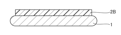
- thermosetting siloxane polymer layer (B) laminated on the first temporary adhesive layer
- the thermoplastic resin layer (A) is (A-1) thermoplastic Resin: 100 parts by mass, (A-2) Curing catalyst: A composition containing more than 0 parts by mass and 1 part by mass or less as an active ingredient (in terms of mass) per 100 parts by mass of component (A-1)
- a temporary adhesive material for wafer processing which is a resin layer
- the thermosetting siloxane polymer layer (B) is a polymer layer cured by the curing catalyst of the (A) layer laminated adjacent to the (B) layer.
- the composite temporary adhesive layer has three layers of the first temporary adhesive layer, the second temporary adhesive layer, and the third temporary adhesive layer, so the adhesive Compared to the case of one layer or two layers, the number of materials to be handled increases, and the number of processes for forming the composite temporary adhesive material layer also increases.
- the present invention has been made in view of the above-mentioned circumstances, and a laminate that can be produced by suppressing the number of precursor layers when producing an adhesive layer while being able to separate a support substrate and a semiconductor substrate. It is an object of the present invention to provide a method for manufacturing a body, a method for manufacturing a processed semiconductor substrate using the method for manufacturing the laminate, and a kit of an adhesive composition that can be used therefor.
- the present invention includes the following. [1] A step of forming a first adhesive coating layer on the surface of a support substrate; forming a second adhesive coating layer on the surface of the semiconductor substrate; The first adhesive coating layer and the second adhesive coating layer are laminated and heated to form the adhesive layer from the first adhesive coating layer and the second adhesive coating layer. and including wherein the first adhesive coating layer is formed from a first adhesive composition; wherein the second adhesive coating layer is formed from a second adhesive composition; The first adhesive composition and the second adhesive composition satisfy the following (1) or (2), A method for manufacturing a laminate.
- the first adhesive composition contains a first thermosetting component and a second thermosetting component that reacts with the first thermosetting component in the presence of a catalyst, and the second contains the catalyst, and at least one of the first adhesive composition and the second adhesive composition contains a release agent component.
- the second adhesive composition contains a first thermosetting component and a second thermosetting component that reacts with the first thermosetting component in the presence of a catalyst, and contains the catalyst, and at least one of the first adhesive composition and the second adhesive composition contains a release agent component.
- the first thermosetting component has an alkenyl group having 2 to 40 carbon atoms bonded to a silicon atom; the second thermosetting component has Si—H groups;
- the catalyst contains a platinum group metal-based catalyst (A2), [1] The method for producing a laminate according to [1].
- the first thermosetting component contains a polyorganosiloxane (a1) having an alkenyl group having 2 to 40 carbon atoms bonded to a silicon atom
- the second thermosetting component contains a polyorganosiloxane (a2) having Si—H groups, [2] The method for manufacturing the laminate described in [2].
- [4] The method for producing a laminate according to any one of [1] to [3], wherein the release agent component contains a non-curable polyorganosiloxane.
- a method for manufacturing a processed semiconductor substrate comprising: a first step of processing the semiconductor substrate of the laminate manufactured by the method of manufacturing the laminate according to any one of [1] to [4]; a second step in which the semiconductor substrate processed in the first step and the support substrate are separated;
- a method of manufacturing a processed semiconductor substrate comprising: [6] containing a first adhesive composition and a second adhesive composition, The first adhesive composition and the second adhesive composition satisfy the following (1) or (2), A kit of adhesive compositions.
- the first adhesive composition contains a first thermosetting component and a second thermosetting component that reacts with the first thermosetting component in the presence of a catalyst, and the second contains the catalyst, and at least one of the first adhesive composition and the second adhesive composition contains a release agent component.
- the second adhesive composition contains a first thermosetting component and a second thermosetting component that reacts with the first thermosetting component in the presence of a catalyst, and contains the catalyst, and at least one of the first adhesive composition and the second adhesive composition contains a release agent component.
- a laminate that can be separated into a support substrate and a semiconductor substrate can be produced while suppressing the number of precursor layers when producing an adhesive layer, and a method for producing a laminate, and the laminate.
- Methods of manufacturing processed semiconductor substrates using the manufacturing methods, as well as kits of adhesive compositions that can be used therein, can be provided.
- a method for manufacturing a laminate of the present invention is a method for manufacturing a laminate having a semiconductor substrate, a support substrate, and an adhesive layer.
- the adhesive layer is provided between the semiconductor substrate and the support substrate.
- the method for producing a laminate of the present invention includes a first adhesive coating layer forming step, a second adhesive coating layer forming step, an adhesive layer forming step, and further includes other steps as necessary.
- the first adhesive coating layer forming step is a step of forming a first adhesive coating layer on the surface of the support substrate.
- the second adhesive coating layer forming step is a step of forming a second adhesive coating layer on the surface of the semiconductor substrate.
- the first adhesive coating layer and the second adhesive coating layer are laminated and heated, and the adhesive layer is formed from the first adhesive coating layer and the second adhesive coating layer. It is the process of forming.
- the first adhesive coating layer is formed from the first adhesive composition.
- a second adhesive coating is formed from a second adhesive composition.
- the first adhesive composition and the second adhesive composition satisfy the following (1) or (2).
- the first adhesive composition contains a first thermosetting component and a second thermosetting component that reacts with the first thermosetting component in the presence of a catalyst.
- the second adhesive composition contains a catalyst. At least one of the first adhesive composition and the second adhesive composition contains a release agent component.
- the second adhesive composition contains a first thermosetting component and a second thermosetting component that reacts with the first thermosetting component in the presence of a catalyst.
- the first adhesive composition contains a catalyst. At least one of the first adhesive composition and the second adhesive composition contains a release agent component.
- the adhesive layer to be formed contains a release agent component. It can be manufactured while suppressing the number of layers.
- the combination of the first thermosetting component and the second thermosetting component and the catalyst for forming the adhesive layer comprise the first adhesive composition and the second It is divided into two adhesive compositions. Therefore, curing does not progress until the first adhesive coating layer and the second adhesive coating layer are bonded together. Therefore, even if the first adhesive composition and the second adhesive composition do not contain a polymerization inhibitor, their pot lives can be lengthened.
- the pot life until bonding after forming the first adhesive coating layer and the second adhesive coating layer, respectively is determined by using the first thermosetting component, the second thermosetting component, and the catalyst. It can be longer than the usable time from forming the adhesive coating layer from the contained adhesive composition to bonding the semiconductor substrate and the supporting substrate together.
- the first adhesive coating layer forming step is a step of forming a first adhesive coating layer on the surface of the support substrate.
- the first adhesive coating layer is formed from the first adhesive composition. Specific examples of the support substrate and the first adhesive composition will be described later.
- the second adhesive coating layer forming step is a step of forming a second adhesive coating layer on the surface of the semiconductor substrate.
- a second adhesive coating is formed from a second adhesive composition. Specific examples of the semiconductor substrate and the second adhesive composition will be described later.
- the order of the first adhesive coating layer forming step and the second adhesive coating layer forming step is not particularly limited.
- the first adhesive coating layer is formed from the first adhesive composition.
- a second adhesive coating is formed from a second adhesive composition.
- Examples of the method of forming the first adhesive coating layer from the first adhesive composition include coating.
- the coating method is usually spin coating.
- Examples of the method of forming the first adhesive coating layer from the first adhesive composition include a method of applying the first adhesive composition to the surface of the release agent coating layer and heating.
- As another method for forming the first adhesive coating layer from the first adhesive composition a coating film is separately formed from the first adhesive composition by a spin coating method or the like, and a sheet-like coating film is obtained. can be applied to the surface of the release agent coating layer as the first adhesive coating layer.
- Examples of the method of forming the second adhesive coating layer from the second adhesive composition include coating.
- the coating method is usually spin coating.
- a method of forming the second adhesive coating layer from the second adhesive composition includes, for example, a method of applying the second adhesive composition to the surface of the semiconductor substrate and heating.
- a coating film is separately formed from the second adhesive composition by a spin coating method or the like, and a sheet-like coating film is obtained. can be applied to the surface of the semiconductor substrate as the second adhesive coating layer.
- the heating temperature of the first or second adhesive composition applied depends on the type and amount of the adhesive component contained in the first or second adhesive composition, whether or not a solvent is contained, and the type of solvent used. Although it cannot be defined unconditionally because it varies depending on the boiling point, the desired thickness of the adhesive layer, etc., it is usually 80 to 150° C. and the heating time is usually 30 seconds to 5 minutes.
- the applied first or second adhesive composition is typically heated. Heating can be performed using a hot plate, an oven, or the like.
- the first adhesive composition and the second adhesive composition satisfy the following (1) or (2).
- the first adhesive composition contains a first thermosetting component and a second thermosetting component that reacts with the first thermosetting component in the presence of a catalyst.
- the second adhesive composition contains a catalyst. At least one of the first adhesive composition and the second adhesive composition contains a release agent component.
- the second adhesive composition contains a first thermosetting component and a second thermosetting component that reacts with the first thermosetting component in the presence of a catalyst.
- the first adhesive composition contains a catalyst. At least one of the first adhesive composition and the second adhesive composition contains a release agent component.
- thermosetting component-containing composition the composition containing the first thermosetting component and the second thermosetting component, which is the first adhesive composition or the second adhesive composition, is referred to as "thermosetting component-containing composition ”.
- first adhesive composition or the second adhesive composition, which contains a catalyst is referred to as a "catalyst-containing composition”.
- the film thickness of the first adhesive coating layer or the second adhesive coating layer obtained by applying the thermosetting component-containing composition and heating it if necessary is usually about 1 ⁇ m to 500 ⁇ m, and the final Basically, it is determined as appropriate so as to fall within the range of the thickness of the adhesive layer, which will be described later.
- the thickness of the first adhesive coating layer or the second adhesive coating layer obtained by applying the catalyst-containing composition and heating it if necessary is usually about 100 nm to 100 ⁇ m. , is appropriately determined so as to fall within the range of the thickness of the adhesive layer, which will be described later.
- the support substrate is not particularly limited as long as it is a member that can support the semiconductor substrate when the semiconductor substrate is processed. Examples thereof include a glass support substrate and a silicon support substrate.
- the shape of the support substrate is not particularly limited, but for example, a disk shape can be mentioned. It should be noted that the disk-shaped support substrate does not need to have a perfectly circular surface shape. For example, the periphery of the support substrate may have a linear portion called an orientation flat or a notch. It may have notches.
- the thickness of the disk-shaped support substrate may be appropriately determined according to the size of the semiconductor substrate, and is not particularly limited, but is, for example, 500 to 1,000 ⁇ m.
- the diameter of the disk-shaped support substrate may be appropriately determined according to the size of the semiconductor substrate, and is not particularly limited, but is, for example, 100 to 1,000 mm.
- the support substrate is a glass wafer or silicon wafer with a diameter of 300 mm and a thickness of about 700 ⁇ m.
- the main material constituting the entire semiconductor substrate is not particularly limited as long as it can be used for this type of application, and examples thereof include silicon, silicon carbide, and compound semiconductors.
- the shape of the semiconductor substrate is not particularly limited, but is, for example, a disc shape. It should be noted that the disk-shaped semiconductor substrate does not need to have a perfect circular shape on its surface. It may have notches.
- the thickness of the disk-shaped semiconductor substrate may be appropriately determined according to the purpose of use of the semiconductor substrate, and is not particularly limited, but is, for example, 500 to 1,000 ⁇ m.
- the diameter of the disk-shaped semiconductor substrate may be appropriately determined according to the purpose of use of the semiconductor substrate, and is not particularly limited, but is, for example, 100 to 1,000 mm.
- the semiconductor substrate may have bumps.
- a bump is a projecting terminal.
- the semiconductor substrate has bumps on the support substrate side.
- bumps are usually formed on the surface on which circuits are formed.
- the circuit may be a single layer or multiple layers.
- the shape of the circuit is not particularly limited.
- the surface opposite to the surface having the bumps (back surface) is a surface to be processed.
- the material, size, shape, structure, and density of the bumps on the semiconductor substrate are not particularly limited. Examples of bumps include ball bumps, printed bumps, stud bumps, and plated bumps.
- the bump height, radius and pitch are appropriately determined from the conditions that the bump height is about 1 to 200 ⁇ m, the bump radius is 1 to 200 ⁇ m, and the bump pitch is 1 to 500 ⁇ m.
- Materials for the bumps include, for example, low-melting solder, high-melting solder, tin, indium, gold, silver, and copper.
- the bumps may consist of only a single component, or may consist of multiple components. More specifically, Sn-based alloy plating such as SnAg bumps, SnBi bumps, Sn bumps, and AuSn bumps can be used.
- the bump may have a laminated structure including a metal layer composed of at least one of these components.
- An example of a semiconductor substrate is a silicon wafer with a diameter of 300 mm and a thickness of about 770 ⁇ m.
- the first adhesive composition and the second adhesive composition satisfy the following (1) or (2).
- the first adhesive composition contains a first thermosetting component and a second thermosetting component that reacts with the first thermosetting component in the presence of a catalyst.
- the second adhesive composition contains a catalyst. At least one of the first adhesive composition and the second adhesive composition contains a release agent component.
- the second adhesive composition contains a first thermosetting component and a second thermosetting component that reacts with the first thermosetting component in the presence of a catalyst.
- the first adhesive composition contains a catalyst. At least one of the first adhesive composition and the second adhesive composition contains a release agent component.
- thermosetting component-containing composition which is the first adhesive composition or the second adhesive composition, contains at least a first thermosetting component and a second thermosetting component, and if necessary , and other components such as solvents.
- the catalyst-containing composition which is the first adhesive composition or the second adhesive composition, contains at least a catalyst and, if necessary, other components such as a solvent.
- the catalyst-containing composition may contain either the first thermosetting component or the second thermosetting component.
- the first thermosetting component contained in the catalyst-containing composition is not particularly limited as long as it is the first thermosetting component. It may be the same thermosetting component as the first thermosetting component contained in the component-containing composition, or may be a different thermosetting component.
- the second thermosetting component contained in the catalyst-containing composition is not particularly limited as long as it is the second thermosetting component. It may be the same thermosetting component as the second thermosetting component contained in the component-containing composition, or may be a different thermosetting component.
- the release agent component may be contained in the thermosetting component-containing composition, may be contained in the catalyst-containing composition, or may be contained in both the thermosetting component-containing composition and the catalyst-containing composition. However, at least it is contained in the thermosetting component-containing composition, from the viewpoint of obtaining better adhesion such that peeling does not occur during processing of the semiconductor substrate in the laminate, and processing the semiconductor substrate It is preferable from the viewpoint that the mechanical detachability of the laminated body after debonding becomes better.
- a kit of adhesive compositions is also a subject of the present invention.
- the adhesive composition kit contains a first adhesive composition and a second adhesive composition.
- a first adhesive composition is used to form the first adhesive coating layer.
- a second adhesive composition is used to form the second adhesive coating.
- thermosetting component and the second thermosetting component are not particularly limited as long as they are thermosetting components that react favorably in the presence of a catalyst.
- the first thermosetting component and the second thermosetting component may be thermosetting components that react in the absence of a catalyst.
- the combination of the first thermosetting component, the second thermosetting component, and the catalyst is not particularly limited, but the first thermosetting component has an alkenyl group having 2 to 40 carbon atoms bonded to a silicon atom,
- the second thermosetting component has Si—H groups and the catalyst contains a platinum group metal-based catalyst (A2).
- Alkenyl groups contained in the first thermosetting component and hydrogen atoms (Si—H groups) contained in the second thermosetting component form a crosslinked structure through a hydrosilylation reaction by the platinum group metal-based catalyst (A2). Harden. As a result, a cured film is formed.
- the first thermosetting component preferably contains polyorganosiloxane (a1) having alkenyl groups having 2 to 40 carbon atoms bonded to silicon atoms.
- the second thermosetting component preferably contains a polyorganosiloxane (a2) having Si—H groups.
- the alkenyl group having 2 to 40 carbon atoms may be substituted. Examples of substituents include halogen atoms, nitro groups, cyano groups, amino groups, hydroxy groups, carboxy groups, aryl groups, heteroaryl groups and the like.
- polyorganosiloxane (a1) having an alkenyl group having 2 to 40 carbon atoms bonded to a silicon atom is a siloxane unit (Q' unit) represented by SiO 2 , R 1 'R 2 'R 3 'SiO 1 /2 siloxane units (M' units), R 4 'R 5 'SiO 2/2 siloxane units (D' units) and R 6 'SiO 3/2 siloxane units ( T'units) containing one or more units selected from the group consisting of M'units, D'units and T'units Polyorganosiloxane containing at least one selected from the group consisting of (a1' ).
- Q' unit siloxane unit represented by SiO 2 , R 1 'R 2 'R 3 'SiO 1 /2 siloxane units (M' units), R 4 'R 5 'SiO 2/2 siloxane units (D' units) and R 6 'Si
- Examples of the polyorganosiloxane (a2) having Si—H groups include siloxane units (Q′′ units) represented by SiO 2 and siloxane units represented by R 1 ′′R 2 ′′R 3 ′′SiO 1/2 ( M" units), R4 "R5" siloxane units represented by SiO2 /2 ( D" units) and R6" siloxane units represented by SiO3/2 ( T" units).
- R 1 ' to R 6 ' are groups bonded to a silicon atom and each independently represents an optionally substituted alkyl group or an optionally substituted alkenyl group, and R 1 ' to R 6 At least one of ' is an optionally substituted alkenyl group.
- substituents include halogen atoms, nitro groups, cyano groups, amino groups, hydroxy groups, carboxy groups, aryl groups, heteroaryl groups and the like.
- R 1 ′′ to R 6 ′′ are groups or atoms bonded to a silicon atom and each independently represent an optionally substituted alkyl group or hydrogen atom, but at least one of R 1 ′′ to R 6 ′′ One is a hydrogen atom.
- substituents include halogen atoms, nitro groups, cyano groups, amino groups, hydroxy groups, carboxy groups, aryl groups, heteroaryl groups and the like.
- the alkyl group may be linear, branched or cyclic, but is preferably a linear or branched alkyl group. Yes, preferably 30 or less, more preferably 20 or less, and even more preferably 10 or less.
- optionally substituted linear or branched alkyl groups include methyl, ethyl, n-propyl, i-propyl, n-butyl, i-butyl and s-butyl. group, tertiary butyl group, n-pentyl group, 1-methyl-n-butyl group, 2-methyl-n-butyl group, 3-methyl-n-butyl group, 1,1-dimethyl-n-propyl group, 1,2-dimethyl-n-propyl group, 2,2-dimethyl-n-propyl group, 1-ethyl-n-propyl group, n-hexyl group, 1-methyl-n-pentyl group, 2-methyl-n -pentyl group, 3-methyl-n-pentyl group, 4-methyl-n-pentyl group, 1,1-dimethyl-n-butyl group, 1,2-dimethyl-n-butyl group, 1,3-dimethyl- n-
- optionally substituted cyclic alkyl groups include a cyclopropyl group, a cyclobutyl group, a 1-methyl-cyclopropyl group, a 2-methyl-cyclopropyl group, a cyclopentyl group, a 1-methyl-cyclobutyl group, a 2- methyl-cyclobutyl group, 3-methyl-cyclobutyl group, 1,2-dimethyl-cyclopropyl group, 2,3-dimethyl-cyclopropyl group, 1-ethyl-cyclopropyl group, 2-ethyl-cyclopropyl group, cyclohexyl group , 1-methyl-cyclopentyl group, 2-methyl-cyclopentyl group, 3-methyl-cyclopentyl group, 1-ethyl-cyclobutyl group, 2-ethyl-cyclobutyl group, 3-ethyl-cyclobutyl group, 1,2-dimethyl-cyclobutyl group, 1,3-dimethyl-cycl
- the alkenyl group may be linear or branched, and the number of carbon atoms thereof is not particularly limited, but is usually 2 to 40, preferably 30 or less, more preferably 20 or less, and more preferably 20 or less. It is preferably 10 or less.
- optionally substituted linear or branched alkenyl groups include, but are not limited to, vinyl groups, allyl groups, butenyl groups, pentenyl groups, and the like. 2 to 14, preferably 2 to 10, more preferably 1 to 6. Among them, an ethenyl group and a 2-propenyl group are particularly preferred.
- Specific examples of the optionally substituted cyclic alkenyl group include, but are not limited to, cyclopentenyl, cyclohexenyl and the like, and the number of carbon atoms thereof is usually 4 to 14, preferably 5 to 10, More preferably 5-6.
- Polyorganosiloxane (a1') contains one or more units selected from the group consisting of Q' units, M' units, D' units and T' units, and M' units, D' units and It contains at least one selected from the group consisting of T' units.
- the polyorganosiloxane (a1') two or more polyorganosiloxanes satisfying such conditions may be used in combination.
- Q' units, M' units, D' units and T' units include (Q' unit and M' unit), (D' unit and M' unit), (T' units and M' units), (Q' units and T' units and M' units), but are not limited to these.
- Polyorganosiloxane (a2′) contains one or more units selected from the group consisting of Q′′ units, M′′ units, D′′ units and T′′ units, and M′′ units, D′′ units and It contains at least one selected from the group consisting of T′′ units.
- the polyorganosiloxane (a2′) two or more polyorganosiloxanes satisfying these conditions may be used in combination.
- Preferred combinations of two or more selected from the group consisting of Q′′ units, M′′ units, D′′ units and T′′ units include (M′′ units and D′′ units), (Q′′ units and M′′ units), (Q" units and T" units and M” units).
- Polyorganosiloxane (a1') is composed of siloxane units in which alkyl groups and / or alkenyl groups are bonded to silicon atoms thereof.
- the proportion of alkenyl groups is preferably 0.1 to 50.0 mol%, more preferably 0.5 to 30.0 mol%, and the remaining R 1 ' to R 6 ' can be alkyl groups. .
- Polyorganosiloxane (a2') is composed of siloxane units in which alkyl groups and/or hydrogen atoms are bonded to silicon atoms thereof, and all substituents represented by R 1 ′′ to R 6 ′′ and The ratio of hydrogen atoms in the substituted atoms is preferably 0.1 to 50.0 mol%, more preferably 10.0 to 40.0 mol%, and the remaining R 1 ′′ to R 6 ′′ are alkyl groups and can do.
- the alkenyl group contained in the polyorganosiloxane (a1) and the Si—H bond contained in the polyorganosiloxane (a2) in the first adhesive layer coating layer and the second adhesive coating layer is in the range of 1.0:0.5 to 1.0:0.66.
- the weight-average molecular weight of polysiloxanes such as polyorganosiloxane (a1) and polyorganosiloxane (a2) is not particularly limited, but each is usually 500 to 1,000,000, and the effects of the present invention are realized with good reproducibility. From the viewpoint of doing, it is preferably 5,000 to 50,000.
- the weight-average molecular weight, number-average molecular weight and degree of dispersion of the polyorganosiloxane are determined by, for example, a GPC apparatus (EcoSEC, HLC-8320GPC manufactured by Tosoh Corporation) and a GPC column (TSKgel SuperMultiporeHZ-N manufactured by Tosoh Corporation).
- the viscosities of the polyorganosiloxane (a1) and the polyorganosiloxane (a2) are not particularly limited, but each is usually 10 to 1,000,000 (mPa s), and from the viewpoint of achieving the effects of the present invention with good reproducibility, it is preferable. is 50 to 10000 (mPa ⁇ s).
- the viscosities of polyorganosiloxane (a1) and polyorganosiloxane (a2) are values measured at 25° C. with an E-type rotational viscometer.
- Polyorganosiloxane (a1) and polyorganosiloxane (a2) react with each other to form a film through a hydrosilylation reaction. Therefore, the curing mechanism differs from that via, for example, silanol groups, and therefore any siloxane need not contain silanol groups or functional groups that form silanol groups upon hydrolysis, such as alkyloxy groups. None.
- the catalyst-containing composition contains a platinum group metal-based catalyst (A2).
- A2 platinum group metal-based catalyst is a catalyst for promoting the hydrosilylation reaction between the alkenyl groups of the polyorganosiloxane (a1) and the Si—H groups of the polyorganosiloxane (a2).
- platinum-based metal catalysts include platinum black, platinum chloride, chloroplatinic acid, reactants of chloroplatinic acid and monohydric alcohols, complexes of chloroplatinic acid and olefins, platinum bisacetoacetate, and the like.
- platinum-based catalysts including, but not limited to: Examples of complexes of platinum and olefins include, but are not limited to, complexes of divinyltetramethyldisiloxane and platinum.
- the amount of the platinum group metal-based catalyst (A2) contained in the catalyst-containing composition is not particularly limited, but usually the total amount of the first adhesive layer coating layer and the second adhesive coating layer is polyorganosiloxane ( It ranges from 1.0 to 50.0 ppm based on the total amount of a1) and polyorganosiloxane (a2).
- the content of the catalyst in the catalyst-containing composition is not particularly limited, it is preferably 1 to 20% by mass, more preferably 5 to 10% by mass, based on the membrane constituents.
- At least one of the first adhesive composition and the second adhesive composition contains a release agent component.
- at least one of the thermosetting component-containing composition and the catalyst-containing composition contains a release agent component.
- the release agent component typically includes a non-curable polyorganosiloxane, and specific examples thereof include epoxy group-containing polyorganosiloxane, methyl group-containing polyorganosiloxane, phenyl group-containing polyorganosiloxane, and the like. include but are not limited to: Moreover, a polydimethylsiloxane is mentioned as a release agent component.
- the polydimethylsiloxane may be modified.
- examples of polydimethylsiloxane that may be modified include, but are not limited to, epoxy group-containing polydimethylsiloxane, unmodified polydimethylsiloxane, and phenyl group-containing polydimethylsiloxane.
- polyorganosiloxane that is the release agent component include, but are not limited to, epoxy group-containing polyorganosiloxane, methyl group-containing polyorganosiloxane, and phenyl group-containing polyorganosiloxane.
- the weight-average molecular weight of polyorganosiloxane which is a release agent component, is not particularly limited, but is usually 100,000 to 2,000,000, and preferably 200,000 from the viewpoint of realizing the effects of the present invention with good reproducibility. ⁇ 1,200,000, more preferably 300,000 to 900,000. Further, the degree of dispersion is not particularly limited, but is usually 1.0 to 10.0, preferably 1.5 to 5.0, more preferably 2, from the viewpoint of realizing suitable peeling with good reproducibility. 0 to 3.0.
- the weight-average molecular weight and degree of dispersion can be measured by the methods described above for polyorganosiloxane.
- the viscosity of polyorganosiloxane, which is the release agent component is not particularly limited, but is usually 1,000 to 2,000,000 mm 2 /s.
- epoxy group-containing polyorganosiloxanes examples include those containing siloxane units ( D10 units) represented by R 11 R 12 SiO 2/2 .
- R 11 is a group bonded to a silicon atom and represents an alkyl group
- R 12 is a group bonded to a silicon atom and represents an epoxy group or an organic group containing an epoxy group
- specific examples of the alkyl group are , the above examples can be mentioned.
- the epoxy group in the organic group containing an epoxy group may be an independent epoxy group without being condensed with other rings, and forms a condensed ring with other rings such as a 1,2-epoxycyclohexyl group. may be an epoxy group.
- Specific examples of organic groups containing epoxy groups include, but are not limited to, 3-glycidoxypropyl and 2-(3,4-epoxycyclohexyl)ethyl.
- a preferable example of the epoxy group-containing polyorganosiloxane is epoxy group-containing polydimethylsiloxane, but the present invention is not limited thereto.
- the epoxy group-containing polyorganosiloxane contains the siloxane units ( D10 units) described above, but may contain Q units, M units and/or T units in addition to the D10 units.
- specific examples of the epoxy group-containing polyorganosiloxane include a polyorganosiloxane consisting only of D10 units, a polyorganosiloxane containing D10 units and Q units, and a polyorganosiloxane containing D10 units and M units.
- Polyorganosiloxane containing D10 units and T units Polyorganosiloxane containing D10 units, Q units and M units Polyorganosiloxane containing D10 units, M units and T units , polyorganosiloxanes containing D 10 units, Q units, M units and T units.
- Epoxy group-containing polyorganosiloxane is preferably epoxy group-containing polydimethylsiloxane having an epoxy value of 0.1 to 5.
- the weight average molecular weight is not particularly limited, it is usually 1,500 to 500,000, and preferably 100,000 or less from the viewpoint of suppressing precipitation in the composition.
- epoxy group-containing polyorganosiloxanes include those represented by formulas (E1) to (E3), but are not limited to these.
- methyl group-containing polyorganosiloxane for example, one containing a siloxane unit ( D200 unit) represented by R210R220SiO2 / 2 , preferably a siloxane unit represented by R21R21SiO2 /2 (D 20 units).
- R 210 and R 220 are groups bonded to a silicon atom, each independently representing an alkyl group, at least one of which is a methyl group, and specific examples of the alkyl group are the above-mentioned examples.
- R 21 is a group bonded to a silicon atom and represents an alkyl group, and specific examples of the alkyl group include those mentioned above. Among them, R 21 is preferably a methyl group.
- a preferred example of the methyl group-containing polyorganosiloxane is polydimethylsiloxane, but the present invention is not limited thereto.
- Methyl group-containing polyorganosiloxane contains the above-mentioned siloxane units (D 200 units or D 20 units), but in addition to D 200 units and D 20 units, it may contain Q units, M units and / or T units. .
- methyl group-containing polyorganosiloxane examples include a polyorganosiloxane consisting only of D 200 units, a polyorganosiloxane containing D 200 units and Q units, and a polyorganosiloxane containing D 200 units and M units.
- polyorganosiloxane containing D 200 units and T units polyorganosiloxane containing D 200 units, Q units and M units
- polyorganosiloxane containing D 200 units, M units and T units D 200 units, Q units, M units and T units.
- methyl group-containing polyorganosiloxane examples include a polyorganosiloxane consisting only of D20 units, a polyorganosiloxane containing D20 units and Q units, and a polyorganosiloxane containing D20 units and M units.
- polyorganosiloxane containing D20 units and T units polyorganosiloxane containing D20 units Q units and M units polyorganosiloxane containing D20 units M units T units , D 20 units, Q units, M units and T units.
- methyl group-containing polyorganosiloxane examples include, but are not limited to, those represented by the formula (M1).
- n4 indicates the number of repeating units and is a positive integer.
- phenyl group-containing polyorganosiloxanes examples include those containing siloxane units represented by R 31 R 32 SiO 2/2 (D 30 units).
- R 31 is a group bonded to a silicon atom and represents a phenyl group or an alkyl group
- R 32 is a group bonded to a silicon atom and represents a phenyl group; can be mentioned, but a methyl group is preferred.
- the phenyl group-containing polyorganosiloxane contains the siloxane units ( D30 units) described above, but may contain Q units, M units and/or T units in addition to the D30 units.
- phenyl group-containing polyorganosiloxane examples include a polyorganosiloxane consisting only of D30 units, a polyorganosiloxane containing D30 units and Q units, and a polyorganosiloxane containing D30 units and M units.
- polyorganosiloxane containing D 30 units and T units polyorganosiloxane containing D 30 units Q units and M units polyorganosiloxane containing D 30 units M units T units , D 30 units, Q units, M units and T units.
- phenyl group-containing polyorganosiloxane examples include, but are not limited to, those represented by formula (P1) or (P2).
- Polyorganosiloxane which is a release agent component, may be a commercially available product or a synthesized product.
- Commercially available products of polyorganosiloxane include, for example, WACKERSILICONE FLUID AK series (AK50, AK 350, AK 1000, AK 10000, AK 1000000) manufactured by Wacker Chemi Co., Ltd., GENIOPLAST GUM, and dimethyl silicone manufactured by Shin-Etsu Chemical Co., Ltd.
- phenyl group-containing polyorganosiloxane (PMM-1043, PMM-1025, PDM-0421, PDM-0821), Shin-Etsu Chemical Co., Ltd.
- phenyl group-containing polyorganosiloxane Examples include siloxane (KF50-3000CS), phenyl group-containing polyorganosiloxane (TSF431, TSF433) manufactured by Momentive, but not limited thereto.
- thermosetting component (A) thermosetting component (A)
- the release agent component (B) can be contained in any ratio, but considering the balance between adhesiveness and release properties, the ratio of the thermosetting component (A) and the release agent component (B) is the first In the adhesive coating layer and the second adhesive coating layer, the mass ratio [(A):(B)] is preferably 99.995:0.005 to 30:70, more preferably 99.9:0 .1 to 75:25.
- a polyorganosiloxane (a1) having an alkenyl group having 2 to 40 carbon atoms bonded to a silicon atom, and a polyorganosiloxane (a2) having a Si—H group, and a non-curable polyorganosiloxane (b1 ) is a mass ratio [(a1+a2):(b1)], preferably 99.995:0.005 to 30:70, more preferably 99.9:0.1 to 75:25.
- thermosetting component-containing composition and the catalyst-containing composition may contain a solvent for the purpose of adjusting the viscosity, etc. Specific examples thereof include aliphatic hydrocarbons, aromatic hydrocarbons, ketones, etc. but not limited to these.
- the solvent includes hexane, heptane, octane, nonane, decane, undecane, dodecane, isododecane, menthane, limonene, toluene, xylene, mesitylene, cumene, MIBK (methyl isobutyl ketone), butyl acetate, and diisobutyl.
- examples include, but are not limited to, ketones, 2-octanone, 2-nonanone, 5-nonanone, and the like. Such solvents can be used singly or in combination of two or more.
- thermosetting component-containing composition and the catalyst-containing composition contain a solvent
- the content thereof is not determined as appropriate in consideration of the viscosity of the desired composition, the coating method to be employed, the thickness of the film to be produced, etc. However, it is in the range of about 10 to 90% by mass with respect to the entire composition.
- the catalyst-containing composition may contain polymers other than polyorganosiloxane as other components.
- polymers include thermoplastic resins.
- thermoplastic resins examples include styrene-based elastomers, ethylene-acrylate copolymers, and ethylene-acrylate-glycidyl methacrylate.
- Styrene-based elastomers include, for example, styrene-ethylene-butylene-styrene block copolymer (SEBS), styrene-ethylene-propylene-styrene block copolymer (SEPS), styrene-ethylene-ethylene-propylene-styrene block copolymer.
- SEEPS coalescence
- SBR styrene-butadiene rubber
- NBR acrylonitrile-butadiene rubber
- SIR pyridine-butadiene rubber
- SBS Polystyrene-polyisoprene-polystyrene
- SIS Polystyrene-polyisoprene-polystyrene
- ⁇ -MeSB ⁇ -MeS poly( ⁇ -methylstyrene)-polyisoprene-poly( ⁇ - methylstyrene)
- EP styrene-chloroprene rubber
- SBS styrene-butadiene-styrene
- ethylene-acrylate copolymers examples include ethylene-methyl acrylate copolymers, ethylene-ethyl acrylate copolymers, ethylene-butyl acrylate copolymers, and the like. These may be partially or wholly hydrogenated.
- the content of the resin component (e.g., first thermosetting component, thermoplastic resin) in the catalyst-containing composition is not particularly limited, but is preferably 80 to 99% by mass relative to the membrane component, and more It is preferably 90 to 95% by mass.
- the viscosities of the thermosetting component-containing composition and the catalyst-containing composition are not particularly limited, but are usually 500 to 20,000 mPa ⁇ s, preferably 1,000 to 5,000 mPa ⁇ s at 25°C.
- the viscosities of the thermosetting component-containing composition and the catalyst-containing composition can be changed by changing the types of solvents used, their ratios, the concentration of film-constituting components, etc., in consideration of various factors such as the coating method used and the desired film thickness. can be adjusted with
- thermosetting component-containing composition and the catalyst-containing composition for the purpose of removing foreign matter, during the production of the thermosetting component-containing composition and the catalyst-containing composition or after mixing all the components, the solvent, solution, etc. used are filtered using a filter or the like.
- ⁇ Adhesive Layer Forming Step> the first adhesive coating layer and the second adhesive coating layer are laminated and heated, and the adhesive layer is formed from the first adhesive coating layer and the second adhesive coating layer. It is the process of forming.
- the first adhesive coating layer and the second adhesive coating layer are brought into contact with each other, and if necessary, the semiconductor substrate and the supporting substrate are subjected to heat treatment, pressure reduction treatment, or both.
- a laminate can be obtained by applying a load in the thickness direction of the two layers to adhere the two layers, and then performing a post-heating treatment. It should be noted that whether the treatment conditions of heat treatment, depressurization treatment, or a combination of both are adopted depends on the types of the first adhesive composition and the second adhesive composition, the compatibility of films obtained from both compositions, It is determined as appropriate after considering various circumstances such as the film thickness and desired adhesive strength.
- the heat treatment removes the solvent, softens the first adhesive coating layer and the second adhesive coating layer, and realizes suitable bonding thereof, and the like.
- the temperature is preferably 130° C. or less, more preferably 90° C. or less, and the heating time depends on the heating temperature and the type of adhesive.
- it is usually 30 seconds or more, preferably 1 minute or more, but from the viewpoint of suppressing deterioration of the adhesive layer and other members. , usually 10 minutes or less, preferably 5 minutes or less.
- the first adhesive coating layer and the second adhesive coating layer which are in contact with each other, should be exposed to an atmospheric pressure of 10 to 10,000 Pa.
- the time for decompression treatment is usually 1 to 30 minutes.
- the two layers that are in contact with each other are preferably bonded together by a reduced pressure treatment, more preferably by a combination of heat treatment and reduced pressure treatment.
- the load in the thickness direction of the semiconductor substrate and the support substrate is not particularly limited as long as it does not adversely affect the semiconductor substrate and the support substrate and the two layers therebetween and can firmly adhere them. , usually in the range of 10 to 1,000N.
- the post-heating temperature is preferably 120° C. or higher from the viewpoint of achieving a sufficient curing rate, and is preferably 260° C. or lower from the viewpoint of preventing deterioration of the substrate and each layer.
- the post-heating time is usually 1 minute or more, preferably 5 minutes or more, from the viewpoint of realizing suitable bonding of the substrates and layers constituting the laminate, and suppresses or avoids adverse effects on each layer due to excessive heating. from the standpoint of reducing the time, it is usually 180 minutes or less, preferably 120 minutes or less. Heating can be performed using a hot plate, an oven, or the like. When post-heating is performed using a hot plate, the laminate may be heated with either the semiconductor substrate or the support substrate facing downward. Post-heating is preferred. Note that one purpose of the post-heating treatment is to realize an adhesive layer that is a more suitable self-supporting film. ) is preferably realized.
- the thickness of the adhesive layer provided in the laminate produced in the present invention is not particularly limited, but is usually 5 to 500 ⁇ m, preferably 10 ⁇ m or more, more preferably 20 ⁇ m or more, from the viewpoint of maintaining film strength. , more preferably 30 ⁇ m or more, and from the viewpoint of avoiding non-uniformity due to a thick film, preferably 200 ⁇ m or less, more preferably 150 ⁇ m or less, even more preferably 120 ⁇ m or less, and even more preferably 70 ⁇ m or less.
- a first adhesive coating layer 2A is formed on the surface of the support substrate 3 (FIG. 1).
- the first adhesive application layer 2A is formed from the first adhesive composition.
- the adhesive application layer 2A is formed by applying a first adhesive composition to the surface of the support substrate 3, for example.
- a second adhesive coating layer 2B is formed on the surface of the semiconductor substrate 1 (FIG. 2).
- the second adhesive coating layer 2B is formed from a second adhesive composition.
- the second adhesive coating layer 2B is formed, for example, by coating the surface of the semiconductor substrate 1 with a second adhesive composition.
- the first adhesive coating layer 2A and the second adhesive coating layer 2B are laminated and heated (FIG. 3).
- the adhesive layer 2 is formed by integrating the first adhesive application layer 2A and the second adhesive application layer 2B.
- a laminate having the semiconductor substrate 1, the adhesive layer 2, and the support substrate 3 is obtained (FIG. 4).
- the method of manufacturing a processed semiconductor substrate of the present invention includes at least a first step and a second step, and further includes other steps such as a third step as necessary.
- the first step is a step of processing the semiconductor substrate of the laminate manufactured by the method of manufacturing the laminate of the present invention.
- the second step is a step of separating the semiconductor substrate processed in the first step from the support substrate.
- the third step is a step of cleaning the separated semiconductor substrates with a cleaning composition.
- the processing applied to the semiconductor substrate in the first step is, for example, processing of the side opposite to the circuit surface of the wafer, and includes thinning of the wafer by polishing the back surface of the wafer. After that, through silicon vias (TSV) and the like are formed, and then the thinned wafer is separated from the support substrate to form a wafer stack, which is three-dimensionally mounted. Before or after that, the formation of the wafer rear surface electrode and the like is also performed. During the wafer thinning and TSV processes, heat of about 250 to 350° C. is applied while the wafer is bonded to the supporting substrate.
- the laminate produced by the present invention generally has heat resistance against the load including the adhesive layer. Processing is not limited to the above, and includes, for example, implementation of a semiconductor component mounting process in the case of temporary bonding with a support substrate to support a base material for mounting semiconductor components.
- the second step is not particularly limited as long as the semiconductor substrate processed in the first step is separated from the support substrate.
- a method of mechanically peeling with a device having a sharp portion so-called debonder. Specifically, for example, after inserting the sharp portion between the semiconductor substrate and the support substrate, the semiconductor substrate and the support substrate are separated.
- the surfaces of the separated semiconductor substrates are cleaned by spraying the cleaning composition or immersing the separated semiconductor substrates in the cleaning composition, and then usually rinsed with a solvent and dried. I do.
- the cleaning composition includes the following.
- a detergent composition usually contains a salt and a solvent.
- a suitable example of the cleaning composition includes a cleaning composition containing a quaternary ammonium salt and a solvent.
- the quaternary ammonium salt is composed of a quaternary ammonium cation and an anion, and is not particularly limited as long as it can be used for this type of application.
- Such quaternary ammonium cations typically include tetra(hydrocarbon)ammonium cations.
- hydroxide ions OH ⁇
- halogen ions such as fluorine ions (F ⁇ ), chloride ions (Cl ⁇ ), bromide ions (Br ⁇ ), iodine ions (I ⁇ ), etc.
- tetrafluoroborate ion BF 4 ⁇
- PF 6 ⁇ hexafluorophosphate ion
- the quaternary ammonium salt is preferably a halogen-containing quaternary ammonium salt, more preferably a fluorine-containing quaternary ammonium salt.
- the halogen atom may be contained in the cation or the anion, preferably the anion.
- the fluorine-containing quaternary ammonium salt is tetra(hydrocarbon)ammonium fluoride.
- the hydrocarbon group in the tetra(hydrocarbon)ammonium fluoride include an alkyl group having 1 to 20 carbon atoms, an alkenyl group having 2 to 20 carbon atoms, an alkynyl group having 2 to 20 carbon atoms, and an alkynyl group having 6 to 20 carbon atoms. and the like.
- the tetra(hydrocarbon)ammonium fluoride comprises a tetraalkylammonium fluoride.
- tetraalkylammonium fluoride examples include tetramethylammonium fluoride, tetraethylammonium fluoride, tetrapropylammonium fluoride, tetrabutylammonium fluoride (also referred to as tetrabutylammonium fluoride) and the like. Not limited. Among them, tetrabutylammonium fluoride is preferred.
- Quaternary ammonium salts such as tetra(hydrocarbon)ammonium fluoride may be used as hydrates.
- quaternary ammonium salts such as tetra(hydrocarbon)ammonium fluoride may be used singly or in combination of two or more.
- the amount of the quaternary ammonium salt is not particularly limited as long as it dissolves in the solvent contained in the detergent composition, but is usually 0.1 to 30% by mass of the detergent composition.
- the solvent contained in the detergent composition is not particularly limited as long as it is used for this type of application and dissolves salts such as quaternary ammonium salts, but it is a detergent having excellent detergency. From the viewpoint of obtaining a composition with good reproducibility, and from the viewpoint of obtaining a detergent composition having excellent uniformity by satisfactorily dissolving a salt such as a quaternary ammonium salt, etc., the detergent composition preferably contains one or Contains two or more amide solvents.
- a suitable example of the amide-based solvent is an acid amide derivative represented by formula (Z).
- R 0 represents an ethyl group, a propyl group or an isopropyl group, preferably an ethyl group or an isopropyl group, more preferably an ethyl group.
- R A and R B each independently represent an alkyl group having 1 to 4 carbon atoms. Alkyl groups having 1 to 4 carbon atoms may be linear, branched, or cyclic, and are specifically methyl, ethyl, propyl, isopropyl, cyclopropyl, n-butyl, and isobutyl groups. , s-butyl group, t-butyl group, cyclobutyl group and the like. Among these, RA and RB are preferably a methyl group or an ethyl group, more preferably a methyl group or an ethyl group, and still more preferably a methyl group.
- Examples of acid amide derivatives represented by formula (Z) include N,N-dimethylpropionamide, N,N-diethylpropionamide, N-ethyl-N-methylpropionamide, N,N-dimethylbutyric acid amide, N, N-diethylbutyric acid amide, N-ethyl-N-methylbutyric acid amide, N,N-dimethylisobutyric acid amide, N,N-diethylisobutyric acid amide, N-ethyl-N-methylisobutyric acid amide and the like.
- N,N-dimethylpropionamide and N,N-dimethylisobutyramide are particularly preferred, and N,N-dimethylpropionamide is more preferred.
- the acid amide derivative represented by formula (Z) may be synthesized by a substitution reaction between a corresponding carboxylic acid ester and an amine, or a commercially available product may be used.
- Another example of a preferable amide-based solvent is a lactam compound represented by formula (Y).
- R 101 represents a hydrogen atom or an alkyl group having 1 to 6 carbon atoms
- R 102 represents an alkylene group having 1 to 6 carbon atoms.
- alkyl groups having 1 to 6 carbon atoms include methyl group, ethyl group, n-propyl group, n-butyl group and the like
- specific examples of alkylene groups having 1 to 6 carbon atoms are methylene groups. , ethylene group, trimethylene group, tetramethylene group, pentamethylene group, hexamethylene group and the like, but are not limited thereto.
- lactam compound represented by formula (Y) examples include ⁇ -lactam compound, ⁇ -lactam compound, ⁇ -lactam compound, ⁇ -lactam compound and the like. More than one species can be used in combination.
- the lactam compound represented by formula (Y) includes 1-alkyl-2-pyrrolidone (N-alkyl- ⁇ -butyrolactam), and in a more preferred embodiment, N-methylpyrrolidone (NMP ) or N-ethylpyrrolidone (NEP), and in an even more preferred embodiment, N-methylpyrrolidone (NMP).
- the cleaning composition may contain one or more other organic solvents that are different from the amide compounds described above.
- Such other organic solvents are used for this type of application, and are not particularly limited as long as they are compatible with the above-mentioned amide compound.
- Other preferred solvents include, but are not limited to, alkylene glycol dialkyl ethers, aromatic hydrocarbon compounds, cyclic structure-containing ether compounds, and the like.
- the amount of the other organic solvent different from the above-mentioned amide compound is generally used for cleaning as long as the quaternary ammonium salt contained in the cleaning composition does not precipitate or separate and is uniformly mixed with the above-mentioned amide compound. It is appropriately determined at 95% by mass or less in the solvent contained in the agent composition.
- the cleaning composition may contain water as a solvent, only an organic solvent is usually intentionally used as a solvent from the viewpoint of avoiding substrate corrosion and the like. In this case, it is not denied that the detergent composition contains hydrated water of the salt and a small amount of water contained in the organic solvent.
- the water content of the cleaning composition is usually 5% by mass or less.
- the processed semiconductor substrate manufactured through the third step is satisfactorily cleaned with the cleaning composition, but the cleaning tape or the like is used to remove the processed semiconductor substrate. It does not prevent the surface of the semiconductor substrate that has been subjected to further cleaning, and if necessary, the surface may be further cleaned using a removal tape or the like.
- Example 1 Production of laminate
- the adhesive composition-1 obtained in Preparation Example 1 is spin-coated on a 300 mm silicon wafer (thickness 775 ⁇ m) as a substrate on the device side, and then heated on a hot plate at 120 ° C. for 90 seconds to finally obtain An adhesive coating layer-1 was formed on a silicon wafer as a semiconductor substrate so that the film thickness in the laminate was 30 ⁇ m.
- the adhesive composition-2 obtained in Preparation Example 2 was spin-coated onto a 300 mm silicon wafer (thickness: 775 ⁇ m) as a substrate on the carrier side, heated on a hot plate at 120° C.
- An adhesive coating layer-2 was formed on a silicon wafer serving as a support substrate so that the thickness of the laminate obtained in 1 was 5 ⁇ m. Then, using a bonding device, two silicon wafers are bonded together so as to sandwich the adhesive coating layer-1 and adhesive coating layer-2, followed by post-heating at 200° C. for 10 minutes. A laminate was produced. The bonding was performed at a temperature of 23° C. and a reduced pressure of 1,500 Pa. A necessary number of laminates were manufactured.
- the laminate After thinning the silicon wafer on the device side of the obtained laminate to 50 ⁇ m with a high-rigidity grinder, the laminate is coated with a dicing tape (manufactured by Nitto Denko Co., Ltd.) with the silicon wafer side of the thinned device side facing down. , DU-300) and fixed. A wedge was inserted between the substrate on the device side and the substrate on the carrier side using a substrate peeling apparatus, and the substrate on the carrier side was lifted to perform peeling. After that, Table 1 shows the result of confirming whether or not the substrate can be peeled off and whether cracks or residue of the adhesive composition is observed on the thinned device substrate.
- a dicing tape manufactured by Nitto Denko Co., Ltd.
- Example 1 The examination was performed in the same procedure as in Example 1, except that the bonding was performed without forming the adhesive coating layer-2 on the carrier side. Table 1 shows the evaluation results.
Landscapes
- Chemical & Material Sciences (AREA)
- Engineering & Computer Science (AREA)
- Organic Chemistry (AREA)
- Microelectronics & Electronic Packaging (AREA)
- Manufacturing & Machinery (AREA)
- Computer Hardware Design (AREA)
- Physics & Mathematics (AREA)
- Power Engineering (AREA)
- General Physics & Mathematics (AREA)
- Condensed Matter Physics & Semiconductors (AREA)
- Chemical Kinetics & Catalysis (AREA)
- Adhesives Or Adhesive Processes (AREA)
- Laminated Bodies (AREA)
Abstract
Description
このような接着と分離プロセスのために、ウエハ加工用仮接着材として、以下のウエハ加工用仮接着材が提案されている(特許文献1参照)。
表面に回路面を有し、裏面を加工すべきウエハを支持体に仮接着するためのウエハ加工用仮接着材であって、前記ウエハ加工用仮接着材が、熱可塑性樹脂層(A)からなる第一仮接着材層と、該第一仮接着材層に積層された熱硬化性シロキサン重合体層(B)からなる第二仮接着材層と、該第二仮接着材層に積層された熱硬化性重合体層(C)からなる第三仮接着材層とを有する複合仮接着材層を備えたものであり、前記熱可塑性樹脂層(A)が、(A-1)熱可塑性樹脂:100質量部、(A-2)硬化触媒:前記(A-1)成分100質量部に対して、有効成分(質量換算)として0質量部を超え1質量部以下を含有する組成物の樹脂層であり、前記熱硬化性シロキサン重合体層(B)が、(B)層に隣接して積層された(A)層の硬化触媒によって硬化する重合体層であるウエハ加工用仮接着材。 For example, it is required to have high stress (strong adhesion) in the planar direction during polishing and low stress (weak adhesion) in the vertical direction during removal.
For such bonding and separation processes, the following temporary adhesive material for wafer processing has been proposed as a temporary adhesive material for wafer processing (see Patent Document 1).
A wafer processing temporary adhesive material for temporarily bonding a wafer having a circuit surface on its surface and a back surface to be processed to a support, wherein the wafer processing temporary adhesive material comprises a thermoplastic resin layer (A). A first temporary adhesive layer, a second temporary adhesive layer consisting of a thermosetting siloxane polymer layer (B) laminated on the first temporary adhesive layer, and a second temporary adhesive layer laminated on the second temporary adhesive layer and a composite temporary adhesive layer having a third temporary adhesive layer made of a thermosetting polymer layer (C), wherein the thermoplastic resin layer (A) is (A-1) thermoplastic Resin: 100 parts by mass, (A-2) Curing catalyst: A composition containing more than 0 parts by mass and 1 part by mass or less as an active ingredient (in terms of mass) per 100 parts by mass of component (A-1) A temporary adhesive material for wafer processing, which is a resin layer, wherein the thermosetting siloxane polymer layer (B) is a polymer layer cured by the curing catalyst of the (A) layer laminated adjacent to the (B) layer. .
[1] 支持基板の表面に第1の接着剤塗布層が形成される工程と、
半導体基板の表面に第2の接着剤塗布層が形成される工程と、
前記第1の接着剤塗布層と前記第2の接着剤塗布層との貼り合せ及び加熱が行われ、前記第1の接着剤塗布層及び前記第2の接着剤塗布層から前記接着層が形成される工程と、
を含み、
前記第1の接着剤塗布層が、第1の接着剤組成物から形成され、
前記第2の接着剤塗布層が、第2の接着剤組成物から形成され、
前記第1の接着剤組成物及び前記第2の接着剤組成物が、以下の(1)又は(2)を満たす、
積層体の製造方法。
(1):前記第1の接着剤組成物が、第1の熱硬化成分と、触媒存在下で前記第1の熱硬化成分と反応する第2の熱硬化成分とを含有し、前記第2の接着剤組成物が、前記触媒を含有し、前記第1の接着剤組成物及び前記第2の接着剤組成物の少なくともいずれかが、剥離剤成分を含有する。
(2):前記第2の接着剤組成物が、第1の熱硬化成分と、触媒存在下で前記第1の熱硬化成分と反応する第2の熱硬化成分とを含有し、前記第1の接着剤組成物が、前記触媒を含有し、前記第1の接着剤組成物及び前記第2の接着剤組成物の少なくともいずれかが、剥離剤成分を含有する。
[2] 前記第1の熱硬化成分が、ケイ素原子に結合した炭素数2~40のアルケニル基を有し、
前記第2の熱硬化成分が、Si-H基を有し、
前記触媒が、白金族金属系触媒(A2)を含有する、
[1]に記載の積層体の製造方法。
[3] 前記第1の熱硬化成分が、ケイ素原子に結合した炭素数2~40のアルケニル基を有するポリオルガノシロキサン(a1)を含有し、
前記第2の熱硬化成分が、Si-H基を有するポリオルガノシロキサン(a2)を含有する、
[2]に記載の積層体の製造方法。
[4] 前記剥離剤成分が、非硬化性のポリオルガノシロキサンを含有する、[1]~[3]のいずれかに記載の積層体の製造方法。
[5] 加工された半導体基板の製造方法であって、
[1]~[4]のいずれかに記載の積層体の製造方法によって製造された前記積層体の前記半導体基板が加工される第1工程と、
前記第1工程によって加工された前記半導体基板と前記支持基板とが分離される第2工程と、
を含む、加工された半導体基板の製造方法。
[6] 第1の接着剤組成物及び第2の接着剤組成物を含有し、
前記第1の接着剤組成物及び前記第2の接着剤組成物が、以下の(1)又は(2)を満たす、
接着剤組成物のキット。
(1):前記第1の接着剤組成物が、第1の熱硬化成分と、触媒存在下で前記第1の熱硬化成分と反応する第2の熱硬化成分とを含有し、前記第2の接着剤組成物が、前記触媒を含有し、前記第1の接着剤組成物及び前記第2の接着剤組成物の少なくともいずれかが、剥離剤成分を含有する。
(2):前記第2の接着剤組成物が、第1の熱硬化成分と、触媒存在下で前記第1の熱硬化成分と反応する第2の熱硬化成分とを含有し、前記第1の接着剤組成物が、前記触媒を含有し、前記第1の接着剤組成物及び前記第2の接着剤組成物の少なくともいずれかが、剥離剤成分を含有する。
[7] [1]~[4]のいずれかに記載の積層体の製造方法に用いられる、[6]に記載の接着剤組成物のキット。 That is, the present invention includes the following.
[1] A step of forming a first adhesive coating layer on the surface of a support substrate;
forming a second adhesive coating layer on the surface of the semiconductor substrate;
The first adhesive coating layer and the second adhesive coating layer are laminated and heated to form the adhesive layer from the first adhesive coating layer and the second adhesive coating layer. and
including
wherein the first adhesive coating layer is formed from a first adhesive composition;
wherein the second adhesive coating layer is formed from a second adhesive composition;
The first adhesive composition and the second adhesive composition satisfy the following (1) or (2),
A method for manufacturing a laminate.
(1): The first adhesive composition contains a first thermosetting component and a second thermosetting component that reacts with the first thermosetting component in the presence of a catalyst, and the second contains the catalyst, and at least one of the first adhesive composition and the second adhesive composition contains a release agent component.
(2): The second adhesive composition contains a first thermosetting component and a second thermosetting component that reacts with the first thermosetting component in the presence of a catalyst, and contains the catalyst, and at least one of the first adhesive composition and the second adhesive composition contains a release agent component.
[2] the first thermosetting component has an alkenyl group having 2 to 40 carbon atoms bonded to a silicon atom;
the second thermosetting component has Si—H groups;
The catalyst contains a platinum group metal-based catalyst (A2),
[1] The method for producing a laminate according to [1].
[3] The first thermosetting component contains a polyorganosiloxane (a1) having an alkenyl group having 2 to 40 carbon atoms bonded to a silicon atom,
The second thermosetting component contains a polyorganosiloxane (a2) having Si—H groups,
[2] The method for manufacturing the laminate described in [2].
[4] The method for producing a laminate according to any one of [1] to [3], wherein the release agent component contains a non-curable polyorganosiloxane.
[5] A method for manufacturing a processed semiconductor substrate, comprising:
a first step of processing the semiconductor substrate of the laminate manufactured by the method of manufacturing the laminate according to any one of [1] to [4];
a second step in which the semiconductor substrate processed in the first step and the support substrate are separated;
A method of manufacturing a processed semiconductor substrate, comprising:
[6] containing a first adhesive composition and a second adhesive composition,
The first adhesive composition and the second adhesive composition satisfy the following (1) or (2),
A kit of adhesive compositions.
(1): The first adhesive composition contains a first thermosetting component and a second thermosetting component that reacts with the first thermosetting component in the presence of a catalyst, and the second contains the catalyst, and at least one of the first adhesive composition and the second adhesive composition contains a release agent component.
(2): The second adhesive composition contains a first thermosetting component and a second thermosetting component that reacts with the first thermosetting component in the presence of a catalyst, and contains the catalyst, and at least one of the first adhesive composition and the second adhesive composition contains a release agent component.
[7] The adhesive composition kit according to [6], which is used in the method for producing a laminate according to any one of [1] to [4].
本発明の積層体の製造方法は、半導体基板と支持基板と接着層とを有する積層体を製造する方法である。
積層体において、接着層は、半導体基板と支持基板との間に設けられている。 (Laminate manufacturing method)
A method for manufacturing a laminate of the present invention is a method for manufacturing a laminate having a semiconductor substrate, a support substrate, and an adhesive layer.
In the laminate, the adhesive layer is provided between the semiconductor substrate and the support substrate.
第1の接着剤塗布層形成工程は、支持基板の表面に第1の接着剤塗布層が形成される工程である。
第2の接着剤塗布層形成工程は、半導体基板の表面に第2の接着剤塗布層が形成される工程である。
接着層形成工程は、第1の接着剤塗布層と第2の接着剤塗布層との貼り合せ及び加熱が行われ、第1の接着剤塗布層及び第2の接着剤塗布層から接着層が形成される工程である。
第1の接着剤塗布層は、第1の接着剤組成物から形成される。
第2の接着剤塗布層は、第2の接着剤組成物から形成される。
第1の接着剤組成物及び第2の接着剤組成物は、以下の(1)又は(2)を満たす。
(1):第1の接着剤組成物は、第1の熱硬化成分と、触媒存在下で第1の熱硬化成分と反応する第2の熱硬化成分とを含有する。第2の接着剤組成物は、触媒を含有する。第1の接着剤組成物及び第2の接着剤組成物の少なくともいずれかは、剥離剤成分を含有する。
(2):第2の接着剤組成物は、第1の熱硬化成分と、触媒存在下で第1の熱硬化成分と反応する第2の熱硬化成分とを含有する。第1の接着剤組成物は、触媒を含有する。第1の接着剤組成物及び第2の接着剤組成物の少なくともいずれかは、剥離剤成分を含有する。 The method for producing a laminate of the present invention includes a first adhesive coating layer forming step, a second adhesive coating layer forming step, an adhesive layer forming step, and further includes other steps as necessary. .
The first adhesive coating layer forming step is a step of forming a first adhesive coating layer on the surface of the support substrate.
The second adhesive coating layer forming step is a step of forming a second adhesive coating layer on the surface of the semiconductor substrate.
In the adhesive layer forming step, the first adhesive coating layer and the second adhesive coating layer are laminated and heated, and the adhesive layer is formed from the first adhesive coating layer and the second adhesive coating layer. It is the process of forming.
The first adhesive coating layer is formed from the first adhesive composition.
A second adhesive coating is formed from a second adhesive composition.
The first adhesive composition and the second adhesive composition satisfy the following (1) or (2).
(1): The first adhesive composition contains a first thermosetting component and a second thermosetting component that reacts with the first thermosetting component in the presence of a catalyst. The second adhesive composition contains a catalyst. At least one of the first adhesive composition and the second adhesive composition contains a release agent component.
(2): The second adhesive composition contains a first thermosetting component and a second thermosetting component that reacts with the first thermosetting component in the presence of a catalyst. The first adhesive composition contains a catalyst. At least one of the first adhesive composition and the second adhesive composition contains a release agent component.
また、本発明の積層体の製造方法においては、接着層を形成するための、第1の熱硬化成分及び第2の熱硬化成分の組み合わせと触媒とが、第1の接着剤組成物及び第2の接着剤組成物に分かれている。そのため、第1の接着剤塗布層と第2の接着剤塗布層とを貼り合せるまでは硬化が進行しない。そのため、第1の接着剤組成物及び第2の接着剤組成物に重合抑制剤を含有させなくても、それらの可使時間を長くできる。更に、第1の接着剤塗布層及び第2の接着剤塗布層をそれぞれ形成した後にそれらを貼り合せるまでの可使時間を、第1の熱硬化成分、第2の熱硬化成分、及び触媒を含有する接着剤組成物から接着剤塗布層を形成した後に半導体基板と支持基板とを貼り合せるまでの可使時間よりも長くできる。 According to the method for producing a laminate of the present invention, the adhesive layer to be formed contains a release agent component. It can be manufactured while suppressing the number of layers.
Further, in the method for producing the laminate of the present invention, the combination of the first thermosetting component and the second thermosetting component and the catalyst for forming the adhesive layer comprise the first adhesive composition and the second It is divided into two adhesive compositions. Therefore, curing does not progress until the first adhesive coating layer and the second adhesive coating layer are bonded together. Therefore, even if the first adhesive composition and the second adhesive composition do not contain a polymerization inhibitor, their pot lives can be lengthened. Furthermore, the pot life until bonding after forming the first adhesive coating layer and the second adhesive coating layer, respectively, is determined by using the first thermosetting component, the second thermosetting component, and the catalyst. It can be longer than the usable time from forming the adhesive coating layer from the contained adhesive composition to bonding the semiconductor substrate and the supporting substrate together.
第1の接着剤塗布層形成工程は、支持基板の表面に第1の接着剤塗布層が形成される工程である。
第1の接着剤塗布層は、第1の接着剤組成物から形成される。
支持基板及び第1の接着剤組成物の具体例については、後述する。 <Step of Forming First Adhesive Coating Layer>
The first adhesive coating layer forming step is a step of forming a first adhesive coating layer on the surface of the support substrate.
The first adhesive coating layer is formed from the first adhesive composition.
Specific examples of the support substrate and the first adhesive composition will be described later.
第2の接着剤塗布層形成工程は、半導体基板の表面に第2の接着剤塗布層が形成される工程である。
第2の接着剤塗布層は、第2の接着剤組成物から形成される。
半導体基板及び第2の接着剤組成物の具体例については、後述する。
第1の接着剤塗布層形成工程及び第2の接着剤塗布層形成工程の順序は、特に限定されない。 <Second Adhesive Coating Layer Forming Step>
The second adhesive coating layer forming step is a step of forming a second adhesive coating layer on the surface of the semiconductor substrate.
A second adhesive coating is formed from a second adhesive composition.
Specific examples of the semiconductor substrate and the second adhesive composition will be described later.
The order of the first adhesive coating layer forming step and the second adhesive coating layer forming step is not particularly limited.
第1の接着剤塗布層は、第1の接着剤組成物から形成される。
第2の接着剤塗布層は、第2の接着剤組成物から形成される。 <<First Adhesive Coating Layer and Second Adhesive Coating Layer>>
The first adhesive coating layer is formed from the first adhesive composition.
A second adhesive coating is formed from a second adhesive composition.
第1の接着剤組成物から第1の接着剤塗布層を形成する方法としては、例えば、剥離剤塗布層の表面に第1の接着剤組成物を塗布し、加熱する方法が挙げられる。
また、第1の接着剤組成物から第1の接着剤塗布層を形成する他の方法として、別途スピンコート法等で第1の接着剤組成物から塗布膜を形成し、シート状の塗布膜を、第1の接着剤塗布層として剥離剤塗布層の表面に貼付する方法を採用し得る。 Examples of the method of forming the first adhesive coating layer from the first adhesive composition include coating. The coating method is usually spin coating.
Examples of the method of forming the first adhesive coating layer from the first adhesive composition include a method of applying the first adhesive composition to the surface of the release agent coating layer and heating.
As another method for forming the first adhesive coating layer from the first adhesive composition, a coating film is separately formed from the first adhesive composition by a spin coating method or the like, and a sheet-like coating film is obtained. can be applied to the surface of the release agent coating layer as the first adhesive coating layer.
第2の接着剤組成物から第2の接着剤塗布層を形成する方法としては、例えば、半導体基板の表面に第2の接着剤組成物を塗布し、加熱する方法が挙げられる。
また、第2の接着剤組成物から第2の接着剤塗布層を形成する他の方法として、別途スピンコート法等で第2の接着剤組成物から塗布膜を形成し、シート状の塗布膜を、第2の接着剤塗布層として半導体基板の表面に貼付する方法を採用し得る。 Examples of the method of forming the second adhesive coating layer from the second adhesive composition include coating. The coating method is usually spin coating.
A method of forming the second adhesive coating layer from the second adhesive composition includes, for example, a method of applying the second adhesive composition to the surface of the semiconductor substrate and heating.
As another method for forming the second adhesive coating layer from the second adhesive composition, a coating film is separately formed from the second adhesive composition by a spin coating method or the like, and a sheet-like coating film is obtained. can be applied to the surface of the semiconductor substrate as the second adhesive coating layer.
第1の又は第2の接着剤組成物が溶媒を含む場合、通常、塗布した第1の又は第2の接着剤組成物を加熱する。
加熱は、ホットプレート、オーブン等を用いて行うことができる。 The heating temperature of the first or second adhesive composition applied depends on the type and amount of the adhesive component contained in the first or second adhesive composition, whether or not a solvent is contained, and the type of solvent used. Although it cannot be defined unconditionally because it varies depending on the boiling point, the desired thickness of the adhesive layer, etc., it is usually 80 to 150° C. and the heating time is usually 30 seconds to 5 minutes.
When the first or second adhesive composition contains a solvent, the applied first or second adhesive composition is typically heated.
Heating can be performed using a hot plate, an oven, or the like.
(1):第1の接着剤組成物は、第1の熱硬化成分と、触媒存在下で第1の熱硬化成分と反応する第2の熱硬化成分とを含有する。第2の接着剤組成物は、触媒を含有する。第1の接着剤組成物及び第2の接着剤組成物の少なくともいずれかは、剥離剤成分を含有する。
(2):第2の接着剤組成物は、第1の熱硬化成分と、触媒存在下で第1の熱硬化成分と反応する第2の熱硬化成分とを含有する。第1の接着剤組成物は、触媒を含有する。第1の接着剤組成物及び第2の接着剤組成物の少なくともいずれかは、剥離剤成分を含有する。
以下、第1の接着剤組成物又は第2の接着剤組成物であって、第1の熱硬化成分と、第2の熱硬化成分とを含有する組成物を、「熱硬化成分含有組成物」と称する。
以下、第1の接着剤組成物又は第2の接着剤組成物であって、触媒を含有する組成物を「触媒含有組成物」と称する。 As described above, the first adhesive composition and the second adhesive composition satisfy the following (1) or (2).
(1): The first adhesive composition contains a first thermosetting component and a second thermosetting component that reacts with the first thermosetting component in the presence of a catalyst. The second adhesive composition contains a catalyst. At least one of the first adhesive composition and the second adhesive composition contains a release agent component.
(2): The second adhesive composition contains a first thermosetting component and a second thermosetting component that reacts with the first thermosetting component in the presence of a catalyst. The first adhesive composition contains a catalyst. At least one of the first adhesive composition and the second adhesive composition contains a release agent component.
Hereinafter, the composition containing the first thermosetting component and the second thermosetting component, which is the first adhesive composition or the second adhesive composition, is referred to as "thermosetting component-containing composition ”.
Hereinafter, the first adhesive composition or the second adhesive composition, which contains a catalyst, is referred to as a "catalyst-containing composition".
触媒含有組成物を塗布し、必要があればそれを加熱して得られる第1の接着剤塗布層又は第2の接着剤塗布層の膜厚は、通常100nm~100μm程度であり、最終的に、後述の接着層の厚さの範囲となるように適宜定められる。 The film thickness of the first adhesive coating layer or the second adhesive coating layer obtained by applying the thermosetting component-containing composition and heating it if necessary is usually about 1 μm to 500 μm, and the final Basically, it is determined as appropriate so as to fall within the range of the thickness of the adhesive layer, which will be described later.
The thickness of the first adhesive coating layer or the second adhesive coating layer obtained by applying the catalyst-containing composition and heating it if necessary is usually about 100 nm to 100 μm. , is appropriately determined so as to fall within the range of the thickness of the adhesive layer, which will be described later.
支持基板としては、半導体基板が加工される際に、半導体基板を支持できる部材であれば、特に限定されないが、例えば、ガラス製支持基板、シリコン製支持基板などが挙げられる。 <Supporting substrate>
The support substrate is not particularly limited as long as it is a member that can support the semiconductor substrate when the semiconductor substrate is processed. Examples thereof include a glass support substrate and a silicon support substrate.
円盤状の支持基板の厚さは、半導体基板の大きさなどに応じて適宜定めればよく、特に限定されないが、例えば、500~1,000μmである。
円盤状の支持基板の直径は、半導体基板の大きさなどに応じて適宜定めればよく、特に限定されないが、例えば、100~1,000mmである。 The shape of the support substrate is not particularly limited, but for example, a disk shape can be mentioned. It should be noted that the disk-shaped support substrate does not need to have a perfectly circular surface shape. For example, the periphery of the support substrate may have a linear portion called an orientation flat or a notch. It may have notches.
The thickness of the disk-shaped support substrate may be appropriately determined according to the size of the semiconductor substrate, and is not particularly limited, but is, for example, 500 to 1,000 μm.
The diameter of the disk-shaped support substrate may be appropriately determined according to the size of the semiconductor substrate, and is not particularly limited, but is, for example, 100 to 1,000 mm.
半導体基板全体を構成する主な材質としては、この種の用途に用いられるものであれば特に限定されないが、例えば、シリコン、シリコンカーバイド、化合物半導体などが挙げられる。
半導体基板の形状は、特に限定されないが、例えば、円盤状である。なお、円盤状の半導体基板は、その面の形状が完全な円形である必要はなく、例えば、半導体基板の外周は、オリエンテーション・フラットと呼ばれる直線部を有していてもよいし、ノッチと呼ばれる切込みを有していてもよい。
円盤状の半導体基板の厚さとしては、半導体基板の使用目的などに応じて適宜定めればよく、特に限定されないが、例えば、500~1,000μmである。
円盤状の半導体基板の直径としては、半導体基板の使用目的などに応じて適宜定めればよく、特に限定されないが、例えば、100~1,000mmである。 <Semiconductor substrate>
The main material constituting the entire semiconductor substrate is not particularly limited as long as it can be used for this type of application, and examples thereof include silicon, silicon carbide, and compound semiconductors.
The shape of the semiconductor substrate is not particularly limited, but is, for example, a disc shape. It should be noted that the disk-shaped semiconductor substrate does not need to have a perfect circular shape on its surface. It may have notches.
The thickness of the disk-shaped semiconductor substrate may be appropriately determined according to the purpose of use of the semiconductor substrate, and is not particularly limited, but is, for example, 500 to 1,000 μm.
The diameter of the disk-shaped semiconductor substrate may be appropriately determined according to the purpose of use of the semiconductor substrate, and is not particularly limited, but is, for example, 100 to 1,000 mm.
積層体において、半導体基板がバンプを有する場合、半導体基板は、支持基板側にバンプを有する。
半導体基板において、バンプは、通常、回路が形成された面上に形成されている。回路は、単層であってもよし、多層であってもよい。回路の形状としては特に制限されない。
半導体基板において、バンプを有する面と反対側の面(裏面)は、加工に供される面である。
半導体基板が有するバンプの材質、大きさ、形状、構造、密度としては、特に限定されない。
バンプとしては、例えば、ボールバンプ、印刷バンプ、スタッドバンプ、めっきバンプなどが挙げられる。
通常、バンプ高さ1~200μm程度、バンプ半径1~200μm、バンプピッチ1~500μmという条件からバンプの高さ、半径及びピッチは適宜決定される。
バンプの材質としては、例えば、低融点はんだ、高融点はんだ、スズ、インジウム、金、銀、銅などが挙げられる。バンプは、単一の成分のみで構成されていてもよいし、複数の成分から構成されていてもよい。より具体的には、SnAgバンプ、SnBiバンプ、Snバンプ、AuSnバンプ等のSnを主体とした合金めっき等が挙げられる。
また、バンプは、これらの成分の少なくともいずれかからなる金属層を含む積層構造を有してもよい。 The semiconductor substrate may have bumps. A bump is a projecting terminal.
In the laminate, when the semiconductor substrate has bumps, the semiconductor substrate has bumps on the support substrate side.
In a semiconductor substrate, bumps are usually formed on the surface on which circuits are formed. The circuit may be a single layer or multiple layers. The shape of the circuit is not particularly limited.
In the semiconductor substrate, the surface opposite to the surface having the bumps (back surface) is a surface to be processed.
The material, size, shape, structure, and density of the bumps on the semiconductor substrate are not particularly limited.
Examples of bumps include ball bumps, printed bumps, stud bumps, and plated bumps.
Normally, the bump height, radius and pitch are appropriately determined from the conditions that the bump height is about 1 to 200 μm, the bump radius is 1 to 200 μm, and the bump pitch is 1 to 500 μm.
Materials for the bumps include, for example, low-melting solder, high-melting solder, tin, indium, gold, silver, and copper. The bumps may consist of only a single component, or may consist of multiple components. More specifically, Sn-based alloy plating such as SnAg bumps, SnBi bumps, Sn bumps, and AuSn bumps can be used.
Also, the bump may have a laminated structure including a metal layer composed of at least one of these components.
第1の接着剤組成物及び第2の接着剤組成物は、前述のとおり、以下の(1)又は(2)を満たす。
(1):第1の接着剤組成物は、第1の熱硬化成分と、触媒存在下で第1の熱硬化成分と反応する第2の熱硬化成分とを含有する。第2の接着剤組成物は、触媒を含有する。第1の接着剤組成物及び第2の接着剤組成物の少なくともいずれかは、剥離剤成分を含有する。
(2):第2の接着剤組成物は、第1の熱硬化成分と、触媒存在下で第1の熱硬化成分と反応する第2の熱硬化成分とを含有する。第1の接着剤組成物は、触媒を含有する。第1の接着剤組成物及び第2の接着剤組成物の少なくともいずれかは、剥離剤成分を含有する。 <<First Adhesive Composition and Second Adhesive Composition (Thermosetting Component-Containing Composition and Catalyst-Containing Composition)>>
As described above, the first adhesive composition and the second adhesive composition satisfy the following (1) or (2).
(1): The first adhesive composition contains a first thermosetting component and a second thermosetting component that reacts with the first thermosetting component in the presence of a catalyst. The second adhesive composition contains a catalyst. At least one of the first adhesive composition and the second adhesive composition contains a release agent component.
(2): The second adhesive composition contains a first thermosetting component and a second thermosetting component that reacts with the first thermosetting component in the presence of a catalyst. The first adhesive composition contains a catalyst. At least one of the first adhesive composition and the second adhesive composition contains a release agent component.
第1の接着剤組成物又は第2の接着剤組成物である触媒含有組成物は、触媒を少なくとも含有し、更に必要に応じて、溶媒などのその他の成分を含有する。
触媒含有組成物は、第1の熱硬化成分及び第2の熱硬化成分のいずれかを含有していてもよい。
触媒含有組成物が、第1の熱硬化成分を含有する場合、触媒含有組成物に含有される第1の熱硬化成分は、第1の熱硬化成分である限り、特に制限されず、熱硬化成分含有組成物に含有される第1の熱硬化成分と同じ熱硬化成分であってもよいし、異なる熱硬化成分であってもよい。
触媒含有組成物が、第2の熱硬化成分を含有する場合、触媒含有組成物に含有される第2の熱硬化成分は、第2の熱硬化成分である限り、特に制限されず、熱硬化成分含有組成物に含有される第2の熱硬化成分と同じ熱硬化成分であってもよいし、異なる熱硬化成分であってもよい。
剥離剤成分は、熱硬化成分含有組成物に含有されていてもよいし、触媒含有組成物に含有されていてもよいし、熱硬化成分含有組成物及び触媒含有組成物の両方に含有されていてもよいが、少なくとも熱硬化成分含有組成物に含有されていることが、積層体における半導体基板の加工中に剥がれ等が生じないようなより良好な密着性を得る観点、及び半導体基板を加工した後の積層体の機械的剥離性がより良好になる観点から、好ましい。 The thermosetting component-containing composition, which is the first adhesive composition or the second adhesive composition, contains at least a first thermosetting component and a second thermosetting component, and if necessary , and other components such as solvents.
The catalyst-containing composition, which is the first adhesive composition or the second adhesive composition, contains at least a catalyst and, if necessary, other components such as a solvent.
The catalyst-containing composition may contain either the first thermosetting component or the second thermosetting component.
When the catalyst-containing composition contains the first thermosetting component, the first thermosetting component contained in the catalyst-containing composition is not particularly limited as long as it is the first thermosetting component. It may be the same thermosetting component as the first thermosetting component contained in the component-containing composition, or may be a different thermosetting component.
When the catalyst-containing composition contains the second thermosetting component, the second thermosetting component contained in the catalyst-containing composition is not particularly limited as long as it is the second thermosetting component. It may be the same thermosetting component as the second thermosetting component contained in the component-containing composition, or may be a different thermosetting component.
The release agent component may be contained in the thermosetting component-containing composition, may be contained in the catalyst-containing composition, or may be contained in both the thermosetting component-containing composition and the catalyst-containing composition. However, at least it is contained in the thermosetting component-containing composition, from the viewpoint of obtaining better adhesion such that peeling does not occur during processing of the semiconductor substrate in the laminate, and processing the semiconductor substrate It is preferable from the viewpoint that the mechanical detachability of the laminated body after debonding becomes better.
接着剤組成物のキットは、第1の接着剤組成物及び第2の接着剤組成物を含有する。
第1の接着剤組成物は、第1の接着剤塗布層の形成に用いられる。
第2の接着剤組成物は、第2の接着剤塗布層の形成に用いられる。 A kit of adhesive compositions is also a subject of the present invention.
The adhesive composition kit contains a first adhesive composition and a second adhesive composition.
A first adhesive composition is used to form the first adhesive coating layer.
A second adhesive composition is used to form the second adhesive coating.
第1の熱硬化成分及び第2の熱硬化成分は、触媒存在下で好適に反応する熱硬化成分であれば、特に限定されない。
なお、第1の熱硬化成分及び第2の熱硬化成分は、触媒不存在下で反応する熱硬化成分であってもよい。 <<<first thermosetting component, second thermosetting component, catalyst, and release agent component>>>
The first thermosetting component and the second thermosetting component are not particularly limited as long as they are thermosetting components that react favorably in the presence of a catalyst.
The first thermosetting component and the second thermosetting component may be thermosetting components that react in the absence of a catalyst.
第1の熱硬化成分に含まれるアルケニル基と、第2の熱硬化成分に含まれる水素原子(Si-H基)とが白金族金属系触媒(A2)によるヒドロシリル化反応によって架橋構造を形成し硬化する。その結果、硬化膜が形成される。 The combination of the first thermosetting component, the second thermosetting component, and the catalyst is not particularly limited, but the first thermosetting component has an alkenyl group having 2 to 40 carbon atoms bonded to a silicon atom, Preferably, the second thermosetting component has Si—H groups and the catalyst contains a platinum group metal-based catalyst (A2).
Alkenyl groups contained in the first thermosetting component and hydrogen atoms (Si—H groups) contained in the second thermosetting component form a crosslinked structure through a hydrosilylation reaction by the platinum group metal-based catalyst (A2). Harden. As a result, a cured film is formed.
第2の熱硬化成分は、Si-H基を有するポリオルガノシロキサン(a2)を含有することが好ましい。
ここで、炭素数2~40のアルケニル基は置換されていてもよい。置換基としては、例えば、ハロゲン原子、ニトロ基、シアノ基、アミノ基、ヒドロキシ基、カルボキシ基、アリール基、ヘテロアリール基等が挙げられる。
ケイ素原子に結合した炭素数2~40のアルケニル基を有するポリオルガノシロキサン(a1)の一例は、SiO2で表されるシロキサン単位(Q’単位)、R1’R2’R3’SiO1/2で表されるシロキサン単位(M’単位)、R4’R5’SiO2/2で表されるシロキサン単位(D’単位)及びR6’SiO3/2で表されるシロキサン単位(T’単位)からなる群より選ばれる1種又は2種以上の単位を含むとともに、M’単位、D’単位及びT’単位からなる群より選ばれる少なくとも1種を含むポリオルガノシロキサン(a1’)である。
Si-H基を有するポリオルガノシロキサン(a2)の一例は、SiO2で表されるシロキサン単位(Q”単位)、R1”R2”R3”SiO1/2で表されるシロキサン単位(M”単位)、R4”R5”SiO2/2で表されるシロキサン単位(D”単位)及びR6”SiO3/2で表されるシロキサン単位(T”単位)からなる群より選ばれる1種又は2種以上の単位を含むとともに、M”単位、D”単位及びT”単位からなる群より選ばれる少なくとも1種を含むポリオルガノシロキサン(a2’)である。 The first thermosetting component preferably contains polyorganosiloxane (a1) having alkenyl groups having 2 to 40 carbon atoms bonded to silicon atoms.
The second thermosetting component preferably contains a polyorganosiloxane (a2) having Si—H groups.
Here, the alkenyl group having 2 to 40 carbon atoms may be substituted. Examples of substituents include halogen atoms, nitro groups, cyano groups, amino groups, hydroxy groups, carboxy groups, aryl groups, heteroaryl groups and the like.
An example of the polyorganosiloxane (a1) having an alkenyl group having 2 to 40 carbon atoms bonded to a silicon atom is a siloxane unit (Q' unit) represented by SiO 2 , R 1 'R 2 'R 3 'SiO 1 /2 siloxane units (M' units), R 4 'R 5 'SiO 2/2 siloxane units (D' units) and R 6 'SiO 3/2 siloxane units ( T'units) containing one or more units selected from the group consisting of M'units, D'units and T'units Polyorganosiloxane containing at least one selected from the group consisting of (a1' ).
Examples of the polyorganosiloxane (a2) having Si—H groups include siloxane units (Q″ units) represented by SiO 2 and siloxane units represented by R 1 ″R 2 ″R 3 ″SiO 1/2 ( M" units), R4 "R5" siloxane units represented by SiO2 /2 ( D" units) and R6" siloxane units represented by SiO3/2 ( T" units). A polyorganosiloxane (a2′) containing one or more units selected from the group consisting of M″ units, D″ units and T″ units.
置換されていてもよい環状アルケニル基の具体例としては、シクロペンテニル、シクロヘキセニル等が挙げられるが、これらに限定されず、その炭素数は、通常4~14であり、好ましくは5~10、より好ましくは5~6である。 Specific examples of optionally substituted linear or branched alkenyl groups include, but are not limited to, vinyl groups, allyl groups, butenyl groups, pentenyl groups, and the like. 2 to 14, preferably 2 to 10, more preferably 1 to 6. Among them, an ethenyl group and a 2-propenyl group are particularly preferred.
Specific examples of the optionally substituted cyclic alkenyl group include, but are not limited to, cyclopentenyl, cyclohexenyl and the like, and the number of carbon atoms thereof is usually 4 to 14, preferably 5 to 10, More preferably 5-6.
なお、本発明において、ポリオルガノシロキサンの重量平均分子量及び数平均分子量並びに分散度は、例えば、GPC装置(東ソー(株)製EcoSEC,HLC-8320GPC)及びGPCカラム(東ソー(株)TSKgel SuperMultiporeHZ-N, TSKgel SuperMultiporeHZ-H)を用い、カラム温度を40℃とし、溶離液(溶出溶媒)としてテトラヒドロフランを用い、流量(流速)を0.35mL/分とし、標準試料としてポリスチレン(昭和電工(株)製、Shodex)を用いて、測定することができる。 The weight-average molecular weight of polysiloxanes such as polyorganosiloxane (a1) and polyorganosiloxane (a2) is not particularly limited, but each is usually 500 to 1,000,000, and the effects of the present invention are realized with good reproducibility. From the viewpoint of doing, it is preferably 5,000 to 50,000.
In the present invention, the weight-average molecular weight, number-average molecular weight and degree of dispersion of the polyorganosiloxane are determined by, for example, a GPC apparatus (EcoSEC, HLC-8320GPC manufactured by Tosoh Corporation) and a GPC column (TSKgel SuperMultiporeHZ-N manufactured by Tosoh Corporation). , TSKgel SuperMultiporeHZ-H), the column temperature was set to 40 ° C., tetrahydrofuran was used as the eluent (elution solvent), the flow rate (flow rate) was set to 0.35 mL / min, and polystyrene (manufactured by Showa Denko Co., Ltd.) was used as a standard sample. , Shodex).
このような白金系の金属触媒は、ポリオルガノシロキサン(a1)のアルケニル基とポリオルガノシロキサン(a2)のSi-H基とのヒドロシリル化反応を促進するための触媒である。 In a preferred embodiment of the present invention, the catalyst-containing composition contains a platinum group metal-based catalyst (A2).
Such a platinum-based metal catalyst is a catalyst for promoting the hydrosilylation reaction between the alkenyl groups of the polyorganosiloxane (a1) and the Si—H groups of the polyorganosiloxane (a2).
白金とオレフィン類との錯体としては、例えばジビニルテトラメチルジシロキサンと白金との錯体が挙げられるが、これに限定されない。
触媒含有組成物に含有される白金族金属系触媒(A2)の量は、特に限定されないが、通常、第1の接着層塗布層及び第2の接着剤塗布層の合計における、ポリオルガノシロキサン(a1)及びポリオルガノシロキサン(a2)の合計量に対して、1.0~50.0ppmの範囲である。 Specific examples of platinum-based metal catalysts include platinum black, platinum chloride, chloroplatinic acid, reactants of chloroplatinic acid and monohydric alcohols, complexes of chloroplatinic acid and olefins, platinum bisacetoacetate, and the like. platinum-based catalysts including, but not limited to:
Examples of complexes of platinum and olefins include, but are not limited to, complexes of divinyltetramethyldisiloxane and platinum.
The amount of the platinum group metal-based catalyst (A2) contained in the catalyst-containing composition is not particularly limited, but usually the total amount of the first adhesive layer coating layer and the second adhesive coating layer is polyorganosiloxane ( It ranges from 1.0 to 50.0 ppm based on the total amount of a1) and polyorganosiloxane (a2).
剥離剤成分として、典型的には、非硬化性のポリオルガノシロキサンが挙げられ、その具体例としては、エポキシ基含有ポリオルガノシロキサン、メチル基含有ポリオルガノシロキサン、フェニル基含有ポリオルガノシロキサン等が挙げられるが、これらに限定されない。
また、剥離剤成分としては、ポリジメチルシロキサンが挙げられる。当該ポリジメチルシロキサンは変性されていてもよい。変性されていてもよいポリジメチルシロキサンとしては、例えば、エポキシ基含有ポリジメチルシロキサン、無変性のポリジメチルシロキサン、フェニル基含有ポリジメチルシロキサン等が挙げられるが、これらに限定されない。 At least one of the first adhesive composition and the second adhesive composition contains a release agent component. In other words, at least one of the thermosetting component-containing composition and the catalyst-containing composition contains a release agent component. By including a release agent component in at least one of the first adhesive composition and the second adhesive composition, the obtained adhesive layer can be suitably peeled off with good reproducibility.
The release agent component typically includes a non-curable polyorganosiloxane, and specific examples thereof include epoxy group-containing polyorganosiloxane, methyl group-containing polyorganosiloxane, phenyl group-containing polyorganosiloxane, and the like. include but are not limited to:
Moreover, a polydimethylsiloxane is mentioned as a release agent component. The polydimethylsiloxane may be modified. Examples of polydimethylsiloxane that may be modified include, but are not limited to, epoxy group-containing polydimethylsiloxane, unmodified polydimethylsiloxane, and phenyl group-containing polydimethylsiloxane.
剥離剤成分であるポリオルガノシロキサンの粘度は、特に限定されないが、通常1,000~2,000,000mm2/sである。なお、剥離剤成分であるポリオルガノシロキサンの粘度の値は、動粘度で示され、センチストークス(cSt)=mm2/sである。粘度(mPa・s)を密度(g/cm3)で割って求めることもできる。すなわち、その値は、25℃で測定したE型回転粘度計で測定した粘度と密度から求めることができ、動粘度(mm2/s)=粘度(mPa・s)/密度(g/cm3)という式から算出することができる。 The weight-average molecular weight of polyorganosiloxane, which is a release agent component, is not particularly limited, but is usually 100,000 to 2,000,000, and preferably 200,000 from the viewpoint of realizing the effects of the present invention with good reproducibility. ~1,200,000, more preferably 300,000 to 900,000. Further, the degree of dispersion is not particularly limited, but is usually 1.0 to 10.0, preferably 1.5 to 5.0, more preferably 2, from the viewpoint of realizing suitable peeling with good reproducibility. 0 to 3.0. The weight-average molecular weight and degree of dispersion can be measured by the methods described above for polyorganosiloxane.
The viscosity of polyorganosiloxane, which is the release agent component, is not particularly limited, but is usually 1,000 to 2,000,000 mm 2 /s. The viscosity value of polyorganosiloxane, which is the component of the release agent, is represented by kinematic viscosity, and centistokes (cSt) = mm 2 /s. It can also be obtained by dividing the viscosity (mPa·s) by the density (g/cm 3 ). That is, the value can be obtained from the viscosity and density measured with an E-type rotational viscometer at 25° C., kinematic viscosity (mm 2 /s)=viscosity (mPa·s)/density (g/cm 3 ) can be calculated from the formula:
エポキシ基を含む有機基におけるエポキシ基は、その他の環と縮合せずに、独立したエポキシ基であってもよく、1,2-エポキシシクロヘキシル基のように、その他の環と縮合環を形成しているエポキシ基であってもよい。
エポキシ基を含む有機基の具体例としては、3-グリシドキシプロピル、2-(3,4-エポキシシクロヘキシル)エチルが挙げられるが、これらに限定されない。
本発明において、エポキシ基含有ポリオルガノシロキサンの好ましい一例としては、エポキシ基含有ポリジメチルシロキサンを挙げることができるが、これに限定されない。 R 11 is a group bonded to a silicon atom and represents an alkyl group, R 12 is a group bonded to a silicon atom and represents an epoxy group or an organic group containing an epoxy group, and specific examples of the alkyl group are , the above examples can be mentioned.
The epoxy group in the organic group containing an epoxy group may be an independent epoxy group without being condensed with other rings, and forms a condensed ring with other rings such as a 1,2-epoxycyclohexyl group. may be an epoxy group.
Specific examples of organic groups containing epoxy groups include, but are not limited to, 3-glycidoxypropyl and 2-(3,4-epoxycyclohexyl)ethyl.
In the present invention, a preferable example of the epoxy group-containing polyorganosiloxane is epoxy group-containing polydimethylsiloxane, but the present invention is not limited thereto.
本発明の好ましい態様においては、エポキシ基含有ポリオルガノシロキサンの具体例としては、D10単位のみからなるポリオルガノシロキサン、D10単位とQ単位とを含むポリオルガノシロキサン、D10単位とM単位とを含むポリオルガノシロキサン、D10単位とT単位とを含むポリオルガノシロキサン、D10単位とQ単位とM単位とを含むポリオルガノシロキサン、D10単位とM単位とT単位とを含むポリオルガノシロキサン、D10単位とQ単位とM単位とT単位とを含むポリオルガノシロキサン等が挙げられる。 The epoxy group-containing polyorganosiloxane contains the siloxane units ( D10 units) described above, but may contain Q units, M units and/or T units in addition to the D10 units.
In a preferred embodiment of the present invention, specific examples of the epoxy group-containing polyorganosiloxane include a polyorganosiloxane consisting only of D10 units, a polyorganosiloxane containing D10 units and Q units, and a polyorganosiloxane containing D10 units and M units. Polyorganosiloxane containing D10 units and T units Polyorganosiloxane containing D10 units, Q units and M units Polyorganosiloxane containing D10 units, M units and T units , polyorganosiloxanes containing D 10 units, Q units, M units and T units.


R21は、ケイ素原子に結合する基であり、アルキル基を表し、アルキル基の具体例としては、上述の例示を挙げることができる。中でも、R21としては、メチル基が好ましい。
本発明において、メチル基含有ポリオルガノシロキサンの好ましい一例としては、ポリジメチルシロキサンを挙げることができるが、これに限定されない。 R 210 and R 220 are groups bonded to a silicon atom, each independently representing an alkyl group, at least one of which is a methyl group, and specific examples of the alkyl group are the above-mentioned examples. can.
R 21 is a group bonded to a silicon atom and represents an alkyl group, and specific examples of the alkyl group include those mentioned above. Among them, R 21 is preferably a methyl group.
In the present invention, a preferred example of the methyl group-containing polyorganosiloxane is polydimethylsiloxane, but the present invention is not limited thereto.


ポリオルガノシロキサンの市販品としては、例えば、ワッカーケミ社製の製品であるWACKERSILICONE FLUID AK シリーズ(AK50、AK 350、AK 1000、AK 10000、AK 1000000)やGENIOPLAST GUM、信越化学工業(株)製 ジメチルシリコーンオイル(KF-96L、KF-96A、KF-96、KF-96H、KF-69、KF-965、KF-968)、環状ジメチルシリコーンオイル(KF-995);ゲレスト社製 エポキシ基含有ポリオルガノシロキサン(商品名CMS-227、ECMS-327)、信越化学工業(株)製 エポキシ基含有ポリオルガノシロキサン(KF-101、KF-1001、KF-1005、X-22-343)、ダウコーニング社製 エポキシ基含有ポリオルガノシロキサン(BY16-839);ゲレスト社製 フェニル基含有ポリオルガノシロキサン(PMM-1043、PMM-1025、PDM-0421、PDM-0821)、信越化学工業(株)製 フェニル基含有ポリオルガノシロキサン(KF50-3000CS)、MOMENTIVE社製 フェニル基含有ポリオルガノシロキサン(TSF431、TSF433)等が挙げられるが、これらに限定されない。 Polyorganosiloxane, which is a release agent component, may be a commercially available product or a synthesized product.
Commercially available products of polyorganosiloxane include, for example, WACKERSILICONE FLUID AK series (AK50, AK 350, AK 1000, AK 10000, AK 1000000) manufactured by Wacker Chemi Co., Ltd., GENIOPLAST GUM, and dimethyl silicone manufactured by Shin-Etsu Chemical Co., Ltd. Oil (KF-96L, KF-96A, KF-96, KF-96H, KF-69, KF-965, KF-968), cyclic dimethyl silicone oil (KF-995); Gelest's epoxy group-containing polyorganosiloxane (trade names CMS-227, ECMS-327), Shin-Etsu Chemical Co., Ltd. epoxy group-containing polyorganosiloxane (KF-101, KF-1001, KF-1005, X-22-343), Dow Corning Epoxy Group-containing polyorganosiloxane (BY16-839); Gelest Co., Ltd. phenyl group-containing polyorganosiloxane (PMM-1043, PMM-1025, PDM-0421, PDM-0821), Shin-Etsu Chemical Co., Ltd. phenyl group-containing polyorganosiloxane Examples include siloxane (KF50-3000CS), phenyl group-containing polyorganosiloxane (TSF431, TSF433) manufactured by Momentive, but not limited thereto.
例えば、ケイ素原子に結合した炭素数2~40のアルケニル基を有するポリオルガノシロキサン(a1)、及びSi-H基を有するポリオルガノシロキサン(a2)の合計と、非硬化性のポリオルガノシロキサン(b1)との比率は、質量比〔(a1+a2):(b1)〕で、好ましくは99.995:0.005~30:70、より好ましくは99.9:0.1~75:25である。 An example of a combination of a thermosetting component-containing composition and a catalyst-containing composition is the sum of the first curing component and the second thermosetting component (here, this sum is referred to as “thermosetting component (A)”) and The release agent component (B) can be contained in any ratio, but considering the balance between adhesiveness and release properties, the ratio of the thermosetting component (A) and the release agent component (B) is the first In the adhesive coating layer and the second adhesive coating layer, the mass ratio [(A):(B)] is preferably 99.995:0.005 to 30:70, more preferably 99.9:0 .1 to 75:25.
For example, a polyorganosiloxane (a1) having an alkenyl group having 2 to 40 carbon atoms bonded to a silicon atom, and a polyorganosiloxane (a2) having a Si—H group, and a non-curable polyorganosiloxane (b1 ) is a mass ratio [(a1+a2):(b1)], preferably 99.995:0.005 to 30:70, more preferably 99.9:0.1 to 75:25.
熱硬化成分含有組成物及び触媒含有組成物は、粘度の調整等を目的に、溶媒を含んでいてもよく、その具体例としては、脂肪族炭化水素、芳香族炭化水素、ケトン等が挙げられるが、これらに限定されない。 <<<solvent>>>
The thermosetting component-containing composition and the catalyst-containing composition may contain a solvent for the purpose of adjusting the viscosity, etc. Specific examples thereof include aliphatic hydrocarbons, aromatic hydrocarbons, ketones, etc. but not limited to these.
触媒含有組成物は、その他の成分として、ポリオルガノシロキサン以外の重合体を含有していてもよい。そのような重合体としては、例えば、熱可塑性樹脂が挙げられる。 <<<Other Ingredients>>>
The catalyst-containing composition may contain polymers other than polyorganosiloxane as other components. Examples of such polymers include thermoplastic resins.
スチレン系エラストマーとしては、例えば、スチレン-エチレン-ブチレン-スチレンブロック共重合体(SEBS)、スチレン-エチレン-プロピレン-スチレンブロック共重合体(SEPS)、スチレン-エチレン-エチレン-プロピレン-スチレンブロック共重合体(SEEPS)、スチレン-ブタジエンゴム(SBR)、アクリロニトリル-ブタジエンゴム(NBR)、ピリジン-ブタジエンゴム、スチレン-イソプレンゴム(SIR)、スチレン-エチレン共重合体、ポリスチレン-ポリブタジエン-ポリスチレン(SBS)、ポリスチレン-ポリイソプレン-ポリスチレン(SIS)、ポリ(α-メチルスチレン)-ポリブタジエン-ポリ(α-メチルスチレン)(α-MeSBα-MeS)、ポリ(α-メチルスチレン)-ポリイソプレン-ポリ(α-メチルスチレン)、エチレン-プロピレン共重合体(EP)、スチレン-クロロプレンゴム(SCR)、スチレン-ブタジエン-スチレン(SBS)共重合体、スチレン-イソプレン-スチレン(SIS)共重合体、スチレン-ポリイソプレンエラストマー、スチレン-ポリブタジエンエラストマー、スチレン-ポリイソプレン-ブタジエンランダムコポリマーなどが挙げられる。
エチレン-アクリレート共重合体としては、例えば、エチレン-メチルアクリレート共重合体、エチレン-エチルアクリレート共重合体、エチレン-ブチルアクリレート共重合体などが挙げられる。
これらは、一部又は全部が水素添加されていてもよい。 Examples of thermoplastic resins include styrene-based elastomers, ethylene-acrylate copolymers, and ethylene-acrylate-glycidyl methacrylate.
Styrene-based elastomers include, for example, styrene-ethylene-butylene-styrene block copolymer (SEBS), styrene-ethylene-propylene-styrene block copolymer (SEPS), styrene-ethylene-ethylene-propylene-styrene block copolymer. coalescence (SEEPS), styrene-butadiene rubber (SBR), acrylonitrile-butadiene rubber (NBR), pyridine-butadiene rubber, styrene-isoprene rubber (SIR), styrene-ethylene copolymer, polystyrene-polybutadiene-polystyrene (SBS), Polystyrene-polyisoprene-polystyrene (SIS), poly(α-methylstyrene)-polybutadiene-poly(α-methylstyrene) (α-MeSBα-MeS), poly(α-methylstyrene)-polyisoprene-poly(α- methylstyrene), ethylene-propylene copolymer (EP), styrene-chloroprene rubber (SCR), styrene-butadiene-styrene (SBS) copolymer, styrene-isoprene-styrene (SIS) copolymer, styrene-polyisoprene Elastomers, styrene-polybutadiene elastomers, styrene-polyisoprene-butadiene random copolymers, and the like.
Examples of ethylene-acrylate copolymers include ethylene-methyl acrylate copolymers, ethylene-ethyl acrylate copolymers, ethylene-butyl acrylate copolymers, and the like.
These may be partially or wholly hydrogenated.
接着層形成工程は、第1の接着剤塗布層と第2の接着剤塗布層との貼り合せ及び加熱が行われ、第1の接着剤塗布層及び第2の接着剤塗布層から接着層が形成される工程である。 <Adhesive Layer Forming Step>
In the adhesive layer forming step, the first adhesive coating layer and the second adhesive coating layer are laminated and heated, and the adhesive layer is formed from the first adhesive coating layer and the second adhesive coating layer. It is the process of forming.
後加熱の時間は、積層体を構成する基板及び層の好適な接合を実現する観点から、通常1分以上、好ましくは5分以上であり、過度の加熱による各層への悪影響等を抑制又は回避する観点から、通常180分以下、好ましくは120分以下である。
加熱は、ホットプレート、オーブン等を用いて行うことができる。ホットプレートを用いて後加熱をする場合、積層体の半導体基板と支持基板のいずれを下にして加熱してもよいが、好適な剥離を再現性よく実現する観点から、半導体基板を下にして後加熱することが好ましい。
なお、後加熱処理の一つの目的は、より好適な自立膜である接着層を実現することであり、第1の熱硬化成分及び第2の熱硬化成分による熱硬化(特にヒドロシリル化反応による硬化)を好適に実現することである。 The post-heating temperature is preferably 120° C. or higher from the viewpoint of achieving a sufficient curing rate, and is preferably 260° C. or lower from the viewpoint of preventing deterioration of the substrate and each layer.
The post-heating time is usually 1 minute or more, preferably 5 minutes or more, from the viewpoint of realizing suitable bonding of the substrates and layers constituting the laminate, and suppresses or avoids adverse effects on each layer due to excessive heating. from the standpoint of reducing the time, it is usually 180 minutes or less, preferably 120 minutes or less.
Heating can be performed using a hot plate, an oven, or the like. When post-heating is performed using a hot plate, the laminate may be heated with either the semiconductor substrate or the support substrate facing downward. Post-heating is preferred.
Note that one purpose of the post-heating treatment is to realize an adhesive layer that is a more suitable self-supporting film. ) is preferably realized.
まず、支持基板3の表面に第1の接着剤塗布層2Aを形成する(図1)。第1の接着剤塗布層2Aは、第1の接着剤組成物から形成される。接着剤塗布層2Aは、例えば、支持基板3の表面に第1の接着剤組成物を塗布することにより形成される。
次に、半導体基板1の表面に第2の接着剤塗布層2Bを形成する(図2)。第2の接着剤塗布層2Bは、第2の接着剤組成物から形成される。第2の接着剤塗布層2Bは、例えば、半導体基板1の表面に第2の接着剤組成物を塗布することにより形成される。
次に、第1の接着剤塗布層2Aと第2の接着剤塗布層2Bとを貼り合せ、加熱する(図3)。そうすると、第1の接着剤塗布層2A及び第2の接着剤塗布層2Bが一体となって接着層2が形成される。その結果、半導体基板1と接着層2と支持基板3とを有する積層体が得られる(図4)。 An example of the method for manufacturing the laminate of the present invention will be described with reference to FIGS. 1 to 4. FIG.
First, a first
Next, a second
Next, the first
本発明の加工された半導体基板の製造方法は、第1工程と、第2工程とを少なくとも含み、更に必要に応じて、第3工程などのその他の工程を含む。
第1工程は、本発明の積層体の製造方法によって製造された積層体の半導体基板が加工される工程である。
第2工程は、第1工程によって加工された半導体基板と支持基板とが分離される工程である。
第3工程は、分離された半導体基板が、洗浄剤組成物で洗浄される工程である。 (Manufacturing method of processed semiconductor substrate)
The method of manufacturing a processed semiconductor substrate of the present invention includes at least a first step and a second step, and further includes other steps such as a third step as necessary.
The first step is a step of processing the semiconductor substrate of the laminate manufactured by the method of manufacturing the laminate of the present invention.
The second step is a step of separating the semiconductor substrate processed in the first step from the support substrate.
The third step is a step of cleaning the separated semiconductor substrates with a cleaning composition.
なお、加工は、上述したものに限定されず、例えば、半導体部品を実装するための基材をサポートするために支持基板と仮接着した場合の半導体部品の実装プロセスの実施等も含まれる。 The processing applied to the semiconductor substrate in the first step is, for example, processing of the side opposite to the circuit surface of the wafer, and includes thinning of the wafer by polishing the back surface of the wafer. After that, through silicon vias (TSV) and the like are formed, and then the thinned wafer is separated from the support substrate to form a wafer stack, which is three-dimensionally mounted. Before or after that, the formation of the wafer rear surface electrode and the like is also performed. During the wafer thinning and TSV processes, heat of about 250 to 350° C. is applied while the wafer is bonded to the supporting substrate. The laminate produced by the present invention generally has heat resistance against the load including the adhesive layer.
Processing is not limited to the above, and includes, for example, implementation of a semiconductor component mounting process in the case of temporary bonding with a support substrate to support a base material for mounting semiconductor components.
例えば、鋭部を有する機材(いわゆるディボンダー)で機械的に剥離する方法が挙げられる。具体的には、例えば、半導体基板と支持基板との間に鋭部を挿入した後、半導体基板と支持基板とを分離する。 The second step is not particularly limited as long as the semiconductor substrate processed in the first step is separated from the support substrate.
For example, there is a method of mechanically peeling with a device having a sharp portion (so-called debonder). Specifically, for example, after inserting the sharp portion between the semiconductor substrate and the support substrate, the semiconductor substrate and the support substrate are separated.
洗浄剤組成物の好適な一例としては、第四級アンモニウム塩と、溶媒とを含む洗浄剤組成物が挙げられる。
第四級アンモニウム塩は、第四級アンモニウムカチオンと、アニオンとから構成されるものであって、この種の用途に用いられるものであれば特に限定されるものではない。
このような第四級アンモニウムカチオンとしては、典型的には、テトラ(炭化水素)アンモニウムカチオンが挙げられる。一方、それと対を成すアニオンとしては、水酸化物イオン(OH-);フッ素イオン(F-)、塩素イオン(Cl-)、臭素イオン(Br-)、ヨウ素イオン(I-)等のハロゲンイオン;テトラフルオロホウ酸イオン(BF4 -);ヘキサフルオロリン酸イオン(PF6 -)等が挙げられるが、これらに限定されない。 A detergent composition usually contains a salt and a solvent.
A suitable example of the cleaning composition includes a cleaning composition containing a quaternary ammonium salt and a solvent.
The quaternary ammonium salt is composed of a quaternary ammonium cation and an anion, and is not particularly limited as long as it can be used for this type of application.
Such quaternary ammonium cations typically include tetra(hydrocarbon)ammonium cations. On the other hand, as the anions forming a pair with it, there are hydroxide ions (OH − ); halogen ions such as fluorine ions (F − ), chloride ions (Cl − ), bromide ions (Br − ), iodine ions (I − ), etc. tetrafluoroborate ion (BF 4 − ); hexafluorophosphate ion (PF 6 − ), etc., but not limited to these.
第四級アンモニウム塩中、ハロゲン原子は、カチオンに含まれていても、アニオンに含まれていてもよいが、好ましくはアニオンに含まれる。 The quaternary ammonium salt is preferably a halogen-containing quaternary ammonium salt, more preferably a fluorine-containing quaternary ammonium salt.
In the quaternary ammonium salt, the halogen atom may be contained in the cation or the anion, preferably the anion.
フッ化テトラ(炭化水素)アンモニウムにおける炭化水素基の具体例としては、炭素数1~20のアルキル基、炭素数2~20のアルケニル基、炭素数2~20のアルキニル基、炭素数6~20のアリール基等が挙げられる。
より好ましい一態様においては、フッ化テトラ(炭化水素)アンモニウムは、フッ化テトラアルキルアンモニウムを含む。
フッ化テトラアルキルアンモニウムの具体例としては、フッ化テトラメチルアンモニウム、フッ化テトラエチルアンモニウム、フッ化テトラプロピルアンモニウム、フッ化テトラブチルアンモニウム(テトラブチルアンモニウムフルオリドともいう)等が挙げられるが、これらに限定されない。中でも、フッ化テトラブチルアンモニウムが好ましい。 In a preferred embodiment, the fluorine-containing quaternary ammonium salt is tetra(hydrocarbon)ammonium fluoride.
Specific examples of the hydrocarbon group in the tetra(hydrocarbon)ammonium fluoride include an alkyl group having 1 to 20 carbon atoms, an alkenyl group having 2 to 20 carbon atoms, an alkynyl group having 2 to 20 carbon atoms, and an alkynyl group having 6 to 20 carbon atoms. and the like.
In a more preferred embodiment, the tetra(hydrocarbon)ammonium fluoride comprises a tetraalkylammonium fluoride.
Specific examples of the tetraalkylammonium fluoride include tetramethylammonium fluoride, tetraethylammonium fluoride, tetrapropylammonium fluoride, tetrabutylammonium fluoride (also referred to as tetrabutylammonium fluoride) and the like. Not limited. Among them, tetrabutylammonium fluoride is preferred.
第四級アンモニウム塩の量は、洗浄剤組成物に含まれる溶媒に溶解する限り特に制限されるものではないが、洗浄剤組成物に対して、通常0.1~30質量%である。 Quaternary ammonium salts such as tetra(hydrocarbon)ammonium fluoride may be used as hydrates. In addition, quaternary ammonium salts such as tetra(hydrocarbon)ammonium fluoride may be used singly or in combination of two or more.
The amount of the quaternary ammonium salt is not particularly limited as long as it dissolves in the solvent contained in the detergent composition, but is usually 0.1 to 30% by mass of the detergent composition.


このようなその他の有機溶媒は、この種の用途に用いられるものであって、上述のアミド化合物と相溶性がある有機溶媒であれば特に限定されるものではない。
好ましいその他の溶媒としては、アルキレングリコールジアルキルエーテル、芳香族炭化水素化合物、環状構造含有エーテル化合物等が挙げられるが、これらに限定されない。
上述のアミド化合物とは異なるその他の有機溶媒の量は、洗浄剤組成物に含まれる第四級アンモニウム塩が析出又は分離せず、かつ上述のアミド化合物と均一に混ざり合う限りにおいて、通常、洗浄剤組成物に含まれる溶媒中95質量%以下で適宜決定される。
なお、洗浄剤組成物は、溶媒として、水を含んでもよいが、基板の腐食等を回避する観点等から、通常、有機溶媒のみが、溶媒として意図して用いられる。なお、この場合において、塩の水和水や、有機溶媒に含まれる微量含まれる水が、洗浄剤組成物に含まれてしまうことまでもが、否定される訳ではない。洗浄剤組成物の含水量は、通常5質量%以下である。 The cleaning composition may contain one or more other organic solvents that are different from the amide compounds described above.
Such other organic solvents are used for this type of application, and are not particularly limited as long as they are compatible with the above-mentioned amide compound.
Other preferred solvents include, but are not limited to, alkylene glycol dialkyl ethers, aromatic hydrocarbon compounds, cyclic structure-containing ether compounds, and the like.
The amount of the other organic solvent different from the above-mentioned amide compound is generally used for cleaning as long as the quaternary ammonium salt contained in the cleaning composition does not precipitate or separate and is uniformly mixed with the above-mentioned amide compound. It is appropriately determined at 95% by mass or less in the solvent contained in the agent composition.
Although the cleaning composition may contain water as a solvent, only an organic solvent is usually intentionally used as a solvent from the viewpoint of avoiding substrate corrosion and the like. In this case, it is not denied that the detergent composition contains hydrated water of the salt and a small amount of water contained in the organic solvent. The water content of the cleaning composition is usually 5% by mass or less.
本発明の加工された半導体基板の製造方法は、上述の工程以外の工程を含んでもよい。 Various changes may be made to the components and methodological elements relating to the above-described steps of the method for manufacturing a processed semiconductor substrate of the present invention without departing from the gist of the present invention.
The method of manufacturing a processed semiconductor substrate of the present invention may include steps other than those described above.
(1)撹拌機:(株)シンキー製 自転公転ミキサー ARE-500
(2)真空貼り合わせ装置:ズースマイクロテック(株)製 XBS300
(3)高剛性研削盤:(株)東京精密製 HRG300
(4)光学式膜厚計(膜厚測定):フィルメトリクス(株)製 F-50
(5)基板剥離装置:ズースマイクロテック(株)製 XBC300 [Device]
(1) Stirrer: Rotation/revolution mixer ARE-500 manufactured by Thinky Co., Ltd.
(2) Vacuum bonding device: XBS300 manufactured by Sus Microtech Co., Ltd.
(3) High-rigidity grinder: HRG300 manufactured by Tokyo Seimitsu Co., Ltd.
(4) Optical film thickness meter (film thickness measurement): F-50 manufactured by Filmetrics Co., Ltd.
(5) Substrate peeling device: XBC300 manufactured by Sus Microtech Co., Ltd.
[調製例1]
撹拌機専用600mL容器に、ポリシロキサン骨格とビニル基とを含有するMQ樹脂(ワッカーケミ社製)34.6g、粘度100mPa・sのSiH基含有直鎖状ポリジメチルシロキサン(ワッカーケミ社製)5.34g、粘度200mPa・sのビニル基含有直鎖状ポリジメチルシロキサン(ワッカーケミ社製)21.8g、粘度5,000,000mPa・sのポリジメチルシロキサンであるポリオルガノシロキサン(ワッカーケミ社製、商品名GENIOPLAST GUM)5.6g、及びp-メンタン(日本テルペン化学(株)製)18.75gを入れ、撹拌機で5分間撹拌し、混合物を得た。
得られた混合物をナイロンフィルター300メッシュでろ過し、接着剤組成物-1を得た。 [1] Preparation of adhesive composition [Preparation Example 1]
34.6 g of MQ resin containing polysiloxane skeleton and vinyl group (manufactured by Wacker Chemi) and 5.34 g of SiH group-containing linear polydimethylsiloxane having a viscosity of 100 mPa s (manufactured by Wacker Chemi) were placed in a 600 mL container dedicated to the stirrer. , 21.8 g of vinyl group-containing linear polydimethylsiloxane (manufactured by Wacker Chemi Co., Ltd.) with a viscosity of 200 mPa s, and polyorganosiloxane (manufactured by Wacker Chemi Co., Ltd., trade name GENIOPLAST GUM), which is a polydimethylsiloxane with a viscosity of 5,000,000 mPa s. ) and 18.75 g of p-menthane (manufactured by Nippon Terpene Chemical Co., Ltd.) were added and stirred with a stirrer for 5 minutes to obtain a mixture.
The resulting mixture was filtered through a nylon filter of 300 mesh to obtain Adhesive Composition-1.
撹拌機専用600mL容器に、ポリシロキサン骨格とビニル基とを含有するMQ樹脂(ワッカーケミ社製)12.5g、白金触媒(ワッカーケミ社製)2.5g、粘度1,000mPa・sのビニル基含有直鎖状ポリジメチルシロキサン(ワッカーケミ社製)25g、及びn-ノナン(東京化成工業(株)製)25g撹拌機で5分間撹拌し、混合物を得た。
得られた混合物をナイロンフィルター300メッシュでろ過し、接着剤組成物-2を得た。 [Preparation Example 2]
In a 600 mL container dedicated to the stirrer, 12.5 g of MQ resin (manufactured by Wacker Chemi) containing a polysiloxane skeleton and vinyl groups, 2.5 g of platinum catalyst (manufactured by Wacker Chemi), and a viscosity of 1,000 mPa s containing vinyl groups were added. 25 g of linear polydimethylsiloxane (manufactured by Wacker Chemie) and 25 g of n-nonane (manufactured by Tokyo Chemical Industry Co., Ltd.) were stirred for 5 minutes with a stirrer to obtain a mixture.
The resulting mixture was filtered through a 300-mesh nylon filter to obtain Adhesive Composition-2.
[実施例1]
調製例1で得られた接着剤組成物-1を、デバイス側の基板として300mmのシリコンウエハー(厚さ775μm)にスピンコートした後に120℃90秒間ホットプレート上で加熱し、最終的に得られる積層体中の膜厚が30μmとなる様に半導体基板であるシリコンウエハー上に接着剤塗布層-1を形成した。
一方、調製例2で得られた接着剤組成物-2を、キャリア側の基板としての300mmのシリコンウエハー(厚さ775μm)にスピンコートした後に120℃90秒間ホットプレート上で加熱し、最終的に得られる積層体中の膜厚が5μmとなる様に支持基板であるシリコンウエハー上に接着剤塗布層-2を形成した。
そして、貼り合せ装置を用いて、二枚のシリコンウエハーを、接着剤塗布層-1及び接着剤塗布層-2を挟み込むように貼り合わせた後、200℃10分間の後加熱処理をすることにより積層体を作製した。なお、貼り合せは、温度23℃、減圧度1,500Paで行った。なお、積層体は、必要な数だけ製造した。
得られた積層体のデバイス側のシリコンウエハーを高剛性研削盤で50μmまで薄化した後、積層体を、薄化したデバイス側のシリコンウエハー側を下にしてダイシングテープ(日東電工(株)製、DU-300)に貼り付け、固定した。
基板剥離装置を用いて、デバイス側の基板とキャリア側の基板の間に楔を挿入し、キャリア側の基板を持ち上げる事で剥離を行った。その後、基板の剥離の可否と、薄化デバイス基板上に割れや接着剤組成物の残渣が見られるか確認した結果を表1に示す。 [2] Production of laminate [Example 1]
The adhesive composition-1 obtained in Preparation Example 1 is spin-coated on a 300 mm silicon wafer (thickness 775 μm) as a substrate on the device side, and then heated on a hot plate at 120 ° C. for 90 seconds to finally obtain An adhesive coating layer-1 was formed on a silicon wafer as a semiconductor substrate so that the film thickness in the laminate was 30 μm.
On the other hand, the adhesive composition-2 obtained in Preparation Example 2 was spin-coated onto a 300 mm silicon wafer (thickness: 775 μm) as a substrate on the carrier side, heated on a hot plate at 120° C. for 90 seconds, and finally An adhesive coating layer-2 was formed on a silicon wafer serving as a support substrate so that the thickness of the laminate obtained in 1 was 5 μm.
Then, using a bonding device, two silicon wafers are bonded together so as to sandwich the adhesive coating layer-1 and adhesive coating layer-2, followed by post-heating at 200° C. for 10 minutes. A laminate was produced. The bonding was performed at a temperature of 23° C. and a reduced pressure of 1,500 Pa. A necessary number of laminates were manufactured.
After thinning the silicon wafer on the device side of the obtained laminate to 50 μm with a high-rigidity grinder, the laminate is coated with a dicing tape (manufactured by Nitto Denko Co., Ltd.) with the silicon wafer side of the thinned device side facing down. , DU-300) and fixed.
A wedge was inserted between the substrate on the device side and the substrate on the carrier side using a substrate peeling apparatus, and the substrate on the carrier side was lifted to perform peeling. After that, Table 1 shows the result of confirming whether or not the substrate can be peeled off and whether cracks or residue of the adhesive composition is observed on the thinned device substrate.
キャリア側に接着剤塗布層-2を形成せずに貼り合わせを実施した以外は実施例1と同様の手順で検討を実施した。評価結果を表1に示す。 [Comparative Example 1]
The examination was performed in the same procedure as in Example 1, except that the bonding was performed without forming the adhesive coating layer-2 on the carrier side. Table 1 shows the evaluation results.

2 接着層
2A 第1の接着剤塗布層
2B 第2の接着剤塗布層
3 支持基板
REFERENCE SIGNS LIST 1
Claims (7)
- 支持基板の表面に第1の接着剤塗布層が形成される工程と、
半導体基板の表面に第2の接着剤塗布層が形成される工程と、
前記第1の接着剤塗布層と前記第2の接着剤塗布層との貼り合せ及び加熱が行われ、前記第1の接着剤塗布層及び前記第2の接着剤塗布層から接着層が形成される工程と、
を含み、
前記第1の接着剤塗布層が、第1の接着剤組成物から形成され、
前記第2の接着剤塗布層が、第2の接着剤組成物から形成され、
前記第1の接着剤組成物及び前記第2の接着剤組成物が、以下の(1)又は(2)を満たす、
積層体の製造方法。
(1):前記第1の接着剤組成物が、第1の熱硬化成分と、触媒存在下で前記第1の熱硬化成分と反応する第2の熱硬化成分とを含有し、前記第2の接着剤組成物が、前記触媒を含有し、前記第1の接着剤組成物及び前記第2の接着剤組成物の少なくともいずれかが、剥離剤成分を含有する。
(2):前記第2の接着剤組成物が、第1の熱硬化成分と、触媒存在下で前記第1の熱硬化成分と反応する第2の熱硬化成分とを含有し、前記第1の接着剤組成物が、前記触媒を含有し、前記第1の接着剤組成物及び前記第2の接着剤組成物の少なくともいずれかが、剥離剤成分を含有する。 forming a first adhesive coating layer on the surface of the support substrate;
forming a second adhesive coating layer on the surface of the semiconductor substrate;
The first adhesive coating layer and the second adhesive coating layer are laminated and heated to form an adhesive layer from the first adhesive coating layer and the second adhesive coating layer. and
including
wherein the first adhesive coating layer is formed from a first adhesive composition;
wherein the second adhesive coating layer is formed from a second adhesive composition;
The first adhesive composition and the second adhesive composition satisfy the following (1) or (2),
A method for manufacturing a laminate.
(1): The first adhesive composition contains a first thermosetting component and a second thermosetting component that reacts with the first thermosetting component in the presence of a catalyst, and the second contains the catalyst, and at least one of the first adhesive composition and the second adhesive composition contains a release agent component.
(2): The second adhesive composition contains a first thermosetting component and a second thermosetting component that reacts with the first thermosetting component in the presence of a catalyst, and contains the catalyst, and at least one of the first adhesive composition and the second adhesive composition contains a release agent component. - 前記第1の熱硬化成分が、ケイ素原子に結合した炭素数2~40のアルケニル基を有し、
前記第2の熱硬化成分が、Si-H基を有し、
前記触媒が、白金族金属系触媒(A2)を含有する、
請求項1に記載の積層体の製造方法。 the first thermosetting component has an alkenyl group having 2 to 40 carbon atoms bonded to a silicon atom;
the second thermosetting component has Si—H groups;
The catalyst contains a platinum group metal-based catalyst (A2),
The manufacturing method of the laminated body of Claim 1. - 前記第1の熱硬化成分が、ケイ素原子に結合した炭素数2~40のアルケニル基を有するポリオルガノシロキサン(a1)を含有し、
前記第2の熱硬化成分が、Si-H基を有するポリオルガノシロキサン(a2)を含有する、
請求項2に記載の積層体の製造方法。 The first thermosetting component contains a polyorganosiloxane (a1) having an alkenyl group having 2 to 40 carbon atoms bonded to a silicon atom,
The second thermosetting component contains a polyorganosiloxane (a2) having Si—H groups,
The method for manufacturing the laminate according to claim 2. - 前記剥離剤成分が、非硬化性のポリオルガノシロキサンを含有する、請求項1に記載の積層体の製造方法。 The method for producing a laminate according to claim 1, wherein the release agent component contains a non-curable polyorganosiloxane.
- 加工された半導体基板の製造方法であって、
請求項1~4のいずれかに記載の積層体の製造方法によって製造された前記積層体の前記半導体基板が加工される第1工程と、
前記第1工程によって加工された前記半導体基板と前記支持基板とが分離される第2工程と、
を含む、加工された半導体基板の製造方法。 A method of manufacturing a processed semiconductor substrate, comprising:
A first step of processing the semiconductor substrate of the laminate manufactured by the method of manufacturing the laminate according to any one of claims 1 to 4;
a second step in which the semiconductor substrate processed in the first step and the support substrate are separated;
A method of manufacturing a processed semiconductor substrate, comprising: - 第1の接着剤組成物及び第2の接着剤組成物を含有し、
前記第1の接着剤組成物及び前記第2の接着剤組成物が、以下の(1)又は(2)を満たす、
接着剤組成物のキット。
(1):前記第1の接着剤組成物が、第1の熱硬化成分と、触媒存在下で前記第1の熱硬化成分と反応する第2の熱硬化成分とを含有し、前記第2の接着剤組成物が、前記触媒を含有し、前記第1の接着剤組成物及び前記第2の接着剤組成物の少なくともいずれかが、剥離剤成分を含有する。
(2):前記第2の接着剤組成物が、第1の熱硬化成分と、触媒存在下で前記第1の熱硬化成分と反応する第2の熱硬化成分とを含有し、前記第1の接着剤組成物が、前記触媒を含有し、前記第1の接着剤組成物及び前記第2の接着剤組成物の少なくともいずれかが、剥離剤成分を含有する。 containing a first adhesive composition and a second adhesive composition;
The first adhesive composition and the second adhesive composition satisfy the following (1) or (2),
A kit of adhesive compositions.
(1): The first adhesive composition contains a first thermosetting component and a second thermosetting component that reacts with the first thermosetting component in the presence of a catalyst, and the second contains the catalyst, and at least one of the first adhesive composition and the second adhesive composition contains a release agent component.
(2): The second adhesive composition contains a first thermosetting component and a second thermosetting component that reacts with the first thermosetting component in the presence of a catalyst, and contains the catalyst, and at least one of the first adhesive composition and the second adhesive composition contains a release agent component. - 請求項1~4のいずれかに記載の積層体の製造方法に用いられる、請求項6に記載の接着剤組成物のキット。 The adhesive composition kit according to claim 6, which is used in the method for producing the laminate according to any one of claims 1 to 4.
Priority Applications (4)
| Application Number | Priority Date | Filing Date | Title |
|---|---|---|---|
| CN202280051910.5A CN117716475A (en) | 2021-07-26 | 2022-07-14 | Method for producing laminate and kit of adhesive composition |
| EP22849268.2A EP4369379A1 (en) | 2021-07-26 | 2022-07-14 | Layered body manufacturing method, and kit for adhesive composition |
| KR1020247003345A KR20240040071A (en) | 2021-07-26 | 2022-07-14 | Method for producing a laminate, and a kit of adhesive composition |
| JP2023538423A JPWO2023008204A1 (en) | 2021-07-26 | 2022-07-14 |
Applications Claiming Priority (2)
| Application Number | Priority Date | Filing Date | Title |
|---|---|---|---|
| JP2021121472 | 2021-07-26 | ||
| JP2021-121472 | 2021-07-26 |
Publications (1)
| Publication Number | Publication Date |
|---|---|
| WO2023008204A1 true WO2023008204A1 (en) | 2023-02-02 |
Family
ID=85086778
Family Applications (1)
| Application Number | Title | Priority Date | Filing Date |
|---|---|---|---|
| PCT/JP2022/027646 WO2023008204A1 (en) | 2021-07-26 | 2022-07-14 | Layered body manufacturing method, and kit for adhesive composition |
Country Status (6)
| Country | Link |
|---|---|
| EP (1) | EP4369379A1 (en) |
| JP (1) | JPWO2023008204A1 (en) |
| KR (1) | KR20240040071A (en) |
| CN (1) | CN117716475A (en) |
| TW (1) | TW202321410A (en) |
| WO (1) | WO2023008204A1 (en) |
Citations (9)
| Publication number | Priority date | Publication date | Assignee | Title |
|---|---|---|---|---|
| WO2015190438A1 (en) * | 2014-06-10 | 2015-12-17 | 日産化学工業株式会社 | Layered body obtained using temporary adhesive agent |
| JP2017013311A (en) | 2015-06-30 | 2017-01-19 | 信越化学工業株式会社 | Temporary adhesive material for waver processing, wafer processed body, and method for manufacturing thin wafer |
| WO2017221772A1 (en) * | 2016-06-22 | 2017-12-28 | 日産化学工業株式会社 | Adhesive containing polydimethylsiloxane |
| WO2019212008A1 (en) * | 2018-05-01 | 2019-11-07 | 日産化学株式会社 | Temporary adhesive containing polysiloxane that contains heat resistant polymerization inhibitor |
| WO2020105586A1 (en) * | 2018-11-19 | 2020-05-28 | 日産化学株式会社 | Adhesive composition for peeling off by irradiation with light, layered product, and production method and peeling-off method for layered product |
| WO2020111069A1 (en) * | 2018-11-28 | 2020-06-04 | 日産化学株式会社 | Adhesive agent composition, layered product and production method for layered product, and method for reducing thickness of semiconductor forming substrate |
| WO2020138240A1 (en) * | 2018-12-27 | 2020-07-02 | 日産化学株式会社 | Adhesive composition for optical irradiation peeling, laminate body, and laminate body production method and peeling method |
| WO2021065547A1 (en) * | 2019-09-30 | 2021-04-08 | 信越化学工業株式会社 | Wafer processed body, temporary adhesive for wafer processing, and method for manufacturing thin wafer |
| WO2021131925A1 (en) * | 2019-12-23 | 2021-07-01 | 日産化学株式会社 | Adhesive composition, laminate and method for producing same, method for peeling laminate, and method for processing semiconductor-forming substrate |
-
2022
- 2022-07-14 CN CN202280051910.5A patent/CN117716475A/en active Pending
- 2022-07-14 WO PCT/JP2022/027646 patent/WO2023008204A1/en active Application Filing
- 2022-07-14 JP JP2023538423A patent/JPWO2023008204A1/ja active Pending
- 2022-07-14 EP EP22849268.2A patent/EP4369379A1/en active Pending
- 2022-07-14 KR KR1020247003345A patent/KR20240040071A/en unknown
- 2022-07-15 TW TW111126737A patent/TW202321410A/en unknown
Patent Citations (9)
| Publication number | Priority date | Publication date | Assignee | Title |
|---|---|---|---|---|
| WO2015190438A1 (en) * | 2014-06-10 | 2015-12-17 | 日産化学工業株式会社 | Layered body obtained using temporary adhesive agent |
| JP2017013311A (en) | 2015-06-30 | 2017-01-19 | 信越化学工業株式会社 | Temporary adhesive material for waver processing, wafer processed body, and method for manufacturing thin wafer |
| WO2017221772A1 (en) * | 2016-06-22 | 2017-12-28 | 日産化学工業株式会社 | Adhesive containing polydimethylsiloxane |
| WO2019212008A1 (en) * | 2018-05-01 | 2019-11-07 | 日産化学株式会社 | Temporary adhesive containing polysiloxane that contains heat resistant polymerization inhibitor |
| WO2020105586A1 (en) * | 2018-11-19 | 2020-05-28 | 日産化学株式会社 | Adhesive composition for peeling off by irradiation with light, layered product, and production method and peeling-off method for layered product |
| WO2020111069A1 (en) * | 2018-11-28 | 2020-06-04 | 日産化学株式会社 | Adhesive agent composition, layered product and production method for layered product, and method for reducing thickness of semiconductor forming substrate |
| WO2020138240A1 (en) * | 2018-12-27 | 2020-07-02 | 日産化学株式会社 | Adhesive composition for optical irradiation peeling, laminate body, and laminate body production method and peeling method |
| WO2021065547A1 (en) * | 2019-09-30 | 2021-04-08 | 信越化学工業株式会社 | Wafer processed body, temporary adhesive for wafer processing, and method for manufacturing thin wafer |
| WO2021131925A1 (en) * | 2019-12-23 | 2021-07-01 | 日産化学株式会社 | Adhesive composition, laminate and method for producing same, method for peeling laminate, and method for processing semiconductor-forming substrate |
Also Published As
| Publication number | Publication date |
|---|---|
| CN117716475A (en) | 2024-03-15 |
| TW202321410A (en) | 2023-06-01 |
| EP4369379A1 (en) | 2024-05-15 |
| KR20240040071A (en) | 2024-03-27 |
| JPWO2023008204A1 (en) | 2023-02-02 |
Similar Documents
| Publication | Publication Date | Title |
|---|---|---|
| JP7460963B2 (en) | Adhesive composition, laminate, method for producing laminate, and method for thinning semiconductor substrate | |
| KR20210126666A (en) | Detergent compositions and cleaning methods | |
| KR20210126668A (en) | Detergent compositions and cleaning methods | |
| KR20210132179A (en) | Detergent compositions and cleaning methods | |
| WO2023008204A1 (en) | Layered body manufacturing method, and kit for adhesive composition | |
| KR20210135542A (en) | Detergent compositions and cleaning methods | |
| WO2022114112A1 (en) | Laminate, method for manufcturing laminate, and method for manufacturing semiconductor substrate | |
| WO2022202029A1 (en) | Multilayer body, method for producing multilayer body, and method for producing semiconductor substrate | |
| TW202126779A (en) | Adhesive composition, laminate and method for producing same, method for peeling laminate, and method for processing semiconductor-forming substrate | |
| TW202146594A (en) | Method for manufacturing semiconductor substrate, method for manufacturing processed semiconductor substrate, and release composition | |
| WO2022202153A1 (en) | Adhesive composition, layered product, method for producing layered product, and method for producing semiconductor substrate | |
| WO2023248872A1 (en) | Remover composition for light irradiation removal | |
| JP7468787B2 (en) | Method for cleaning semiconductor substrates, method for producing processed semiconductor substrates, and composition for stripping and dissolving | |
| JP2023125710A (en) | Adhesive composition for light-irradiation peeling, laminate, method for producing laminate, and method for producing processed semiconductor substrate | |
| WO2023132229A1 (en) | Adhesive agent composition, laminate, method for manufacturing laminate, and method for manufacturing processed substrate | |
| CN117981055A (en) | Method for cleaning semiconductor substrate, method for producing processed semiconductor substrate, and composition for stripping and dissolving | |
| WO2023100705A1 (en) | Releasability imparter, adhesive composition, layered product, and method for producing semiconductor substrate | |
| WO2024062974A1 (en) | Remover composition for light irradiation removal, multilayer body, and method for producing processed semiconductor substrate | |
| WO2022210068A1 (en) | Adhesive composition, laminate, method for manufacturing laminate, and method for manufacturing processed substrate | |
| WO2024058025A1 (en) | Method for cleaning semiconductor substrate, method for producing processed semiconductor substrate, and peeling and dissolving composition | |
| WO2024058018A1 (en) | Method for cleaning semiconductor substrate, method for producing processed semiconductor substrate, and peeling and dissolving composition | |
| KR20240070529A (en) | Method for cleaning semiconductor substrates, method for manufacturing processed semiconductor substrates, and composition for peeling and dissolving | |
| US20240132806A1 (en) | Method for cleaning semiconductor substrate, method for manufacturing processed semiconductor substrate, and peeling and dissolving composition | |
| TW202415758A (en) | Cleaning agent composition and cleaning method | |
| KR20210126667A (en) | Detergent compositions and cleaning methods |
Legal Events
| Date | Code | Title | Description |
|---|---|---|---|
| 121 | Ep: the epo has been informed by wipo that ep was designated in this application |
Ref document number: 22849268 Country of ref document: EP Kind code of ref document: A1 |
|
| WWE | Wipo information: entry into national phase |
Ref document number: 2023538423 Country of ref document: JP |
|
| WWE | Wipo information: entry into national phase |
Ref document number: 202280051910.5 Country of ref document: CN |
|
| ENP | Entry into the national phase |
Ref document number: 20247003345 Country of ref document: KR Kind code of ref document: A |
|
| WWE | Wipo information: entry into national phase |
Ref document number: 2022849268 Country of ref document: EP |
|
| ENP | Entry into the national phase |
Ref document number: 2022849268 Country of ref document: EP Effective date: 20240205 |
|
| NENP | Non-entry into the national phase |
Ref country code: DE |