(実施形態)
[アンテナ素子10の構造]
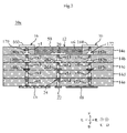
以下に、本発明の一実施形態に係るアンテナ素子10の構造について図面を参照しながら説明する。図1は、アンテナ素子10の分解斜視図である。図2は、図1のA-Aにおけるアンテナ素子10の断面図である。
(Embodiment)
[Structure of antenna element 10]
Hereinafter, the structure of the antenna element 10 according to the embodiment of the present invention will be described with reference to the drawings. FIG. 1 is an exploded perspective view of the antenna element 10. FIG. 2 is a cross-sectional view of the antenna element 10 in AA of FIG.
以下では、アンテナ素子10の絶縁基材12の積層方向を上下方向と定義する。また、アンテナ素子10は、上下方向に見て、長方形状を有している。上下方向に見て、アンテナ素子10の長辺が延びる方向を左右方向と定義する。上下方向に見て、アンテナ素子10の短辺が延びる方向を前後方向と定義する。上下方向、左右方向及び前後方向は、互いに直交している。なお、本明細書における方向の定義は、一例である。従って、アンテナ素子10の実使用時における方向と本明細書における方向とが一致している必要はない。また、各図面において上下方向が反転してもよい。同様に、各図面において左右方向が反転してもよい。各図面において前後方向が反転してもよい。
In the following, the stacking direction of the insulating base material 12 of the antenna element 10 is defined as the vertical direction. Further, the antenna element 10 has a rectangular shape when viewed in the vertical direction. When viewed in the vertical direction, the direction in which the long side of the antenna element 10 extends is defined as the horizontal direction. When viewed in the vertical direction, the direction in which the short side of the antenna element 10 extends is defined as the front-back direction. The vertical direction, the horizontal direction, and the front-back direction are orthogonal to each other. The definition of direction in this specification is an example. Therefore, it is not necessary that the direction of the antenna element 10 in actual use and the direction in the present specification match. Further, the vertical direction may be reversed in each drawing. Similarly, the left-right direction may be reversed in each drawing. The front-back direction may be reversed in each drawing.
以下では、Xは、アンテナ素子10の部品又は部材である。本明細書において、特に断りのない場合には、Xの各部について以下のように定義する。Xの前部とは、Xの前半分を意味する。Xの後部とは、Xの後半分を意味する。Xの左部とは、Xの左半分を意味する。Xの右部とは、Xの右半分を意味する。Xの上部とは、Xの上半分を意味する。Xの下部とは、Xの下半分を意味する。Xの前端とは、Xの前方向の端を意味する。Xの後端とは、Xの後方向の端を意味する。Xの左端とは、Xの左方向の端を意味する。Xの右端とは、Xの右方向の端を意味する。Xの上端とは、Xの上方向の端を意味する。Xの下端とは、Xの下方向の端を意味する。Xの前端部とは、Xの前端及びその近傍を意味する。Xの後端部とは、Xの後端及びその近傍を意味する。Xの左端部とは、Xの左端及びその近傍を意味する。Xの右端部とは、Xの右端及びその近傍を意味する。Xの上端部とは、Xの上端及びその近傍を意味する。Xの下端部とは、Xの下端及びその近傍を意味する。
In the following, X is a component or member of the antenna element 10. Unless otherwise specified, each part of X is defined as follows in the present specification. The front part of X means the front half of X. The rear part of X means the rear half of X. The left part of X means the left half of X. The right part of X means the right half of X. The upper part of X means the upper half of X. The lower part of X means the lower half of X. The front end of X means the front end of X. The rear end of X means the rear end of X. The left end of X means the left end of X. The right end of X means the right end of X. The upper end of X means the upper end of X. The lower end of X means the lower end of X. The front end portion of X means the front end portion of X and its vicinity. The rear end portion of X means the rear end portion of X and its vicinity. The left end portion of X means the left end portion of X and its vicinity. The right end portion of X means the right end portion of X and its vicinity. The upper end portion of X means the upper end portion of X and its vicinity. The lower end portion of X means the lower end portion of X and its vicinity.
アンテナ素子10は、例えば、携帯電話等の電子機器に用いられる。アンテナ素子10は、図1に示すように、絶縁基材12、第1グランド導体16、面状グランド導体層18(第1面状グランド導体層)、第1放射導体層20、信号電極22及び接続部24を備えている。
The antenna element 10 is used in, for example, an electronic device such as a mobile phone. As shown in FIG. 1, the antenna element 10 includes an insulating base material 12, a first ground conductor 16, a planar ground conductor layer 18 (first planar ground conductor layer), a first radiation conductor layer 20, a signal electrode 22, and a signal electrode 22. A connection portion 24 is provided.
絶縁基材12は、板形状を有している。絶縁基材12は、上下方向に見て、長方形状を有している。絶縁基材12は、絶縁体層14a~14eが上下方向に積層された構造を有している。絶縁体層14a~14eは、上から下へとこの順に並んでいる。絶縁体層14a~14dの材料は、ポリイミドや液晶ポリマー等の熱可塑性樹脂である。
The insulating base material 12 has a plate shape. The insulating base material 12 has a rectangular shape when viewed in the vertical direction. The insulating base material 12 has a structure in which insulator layers 14a to 14e are laminated in the vertical direction. The insulator layers 14a to 14e are arranged in this order from top to bottom. The material of the insulator layers 14a to 14d is a thermoplastic resin such as polyimide or a liquid crystal polymer.
第1グランド導体16、面状グランド導体層18及び第1放射導体層20は、パッチアンテナとして機能する。面状グランド導体層18は、絶縁基材12に設けられている。より詳細には、面状グランド導体層18は、絶縁体層14eの下主面に設けられている。これにより、面状グランド導体層18は、絶縁基材12の下主面に設けられている。面状グランド導体層18は、図1に示すように、上下方向に見て、長方形状を有している。面状グランド導体層18の長辺は、左右方向に延びている。面状グランド導体層18の短辺は、前後方向に延びている。面状グランド導体層18は、グランド電位に接続される。
The first ground conductor 16, the planar ground conductor layer 18, and the first radiation conductor layer 20 function as patch antennas. The planar ground conductor layer 18 is provided on the insulating base material 12. More specifically, the planar ground conductor layer 18 is provided on the lower main surface of the insulator layer 14e. As a result, the planar ground conductor layer 18 is provided on the lower main surface of the insulating base material 12. As shown in FIG. 1, the planar ground conductor layer 18 has a rectangular shape when viewed in the vertical direction. The long side of the planar ground conductor layer 18 extends in the left-right direction. The short side of the planar ground conductor layer 18 extends in the front-rear direction. The planar ground conductor layer 18 is connected to the ground potential.
第1放射導体層20は、第1高周波信号を放射及び/又は受信する。第1放射導体層20は、絶縁基材12に設けられている。より詳細には、第1放射導体層20は、絶縁体層14bの上主面に設けられている。よって、第1放射導体層20は、面状グランド導体層18の上に位置している。ここで、第1放射導体層20が面状グランド導体層18の上に配置されるとは、以下の状態を指す。第1放射導体層20の一部は、面状グランド導体層18が上方向に平行移動するときに通過する領域内に配置されている。よって、第1放射導体層20は、面状グランド導体層18が上方向に平行移動するときに通過する領域内に収まっていてもよいし、面状グランド導体層18が上方向に平行移動するときに通過する領域から突出していてもよい。第1放射導体層20の下主面は、上下方向に見て、面状グランド導体層18の上主面と重なっている。
The first radiation conductor layer 20 radiates and / or receives the first high frequency signal. The first radiation conductor layer 20 is provided on the insulating base material 12. More specifically, the first radiation conductor layer 20 is provided on the upper main surface of the insulator layer 14b. Therefore, the first radiating conductor layer 20 is located on the planar ground conductor layer 18. Here, the fact that the first radiating conductor layer 20 is arranged on the planar ground conductor layer 18 means the following state. A part of the first radiating conductor layer 20 is arranged in a region through which the planar ground conductor layer 18 passes when it is translated upward. Therefore, the first radiating conductor layer 20 may be contained in the region through which the planar ground conductor layer 18 is translated when the planar ground conductor layer 18 is translated upward, or the planar ground conductor layer 18 is translated upward. It may sometimes protrude from the area through which it passes. The lower main surface of the first radiating conductor layer 20 overlaps with the upper main surface of the planar ground conductor layer 18 when viewed in the vertical direction.
信号電極22は、絶縁体層14eの下主面に設けられている。信号電極22は、上下方向に見て、面状グランド導体層18により周囲を囲まれている。ただし、信号電極22は、面状グランド導体層18とは絶縁されている。信号電極22には、第1放射導体層20が放射及び/又は受信する第1高周波信号が入出力する。
The signal electrode 22 is provided on the lower main surface of the insulator layer 14e. The signal electrode 22 is surrounded by a planar ground conductor layer 18 when viewed in the vertical direction. However, the signal electrode 22 is insulated from the planar ground conductor layer 18. A first high frequency signal radiated and / or received by the first radiation conductor layer 20 is input / output to the signal electrode 22.
接続部24は、第1放射導体層20と信号電極22とを電気的に接続している。より詳細には、接続部24は、層間接続導体v51~v54及び接続導体層202,204を含んでいる。層間接続導体v51~v54のそれぞれは、絶縁体層14b~14eを上下方向に貫通している。接続導体層202は、層間接続導体v51と層間接続導体v52との間に設けられている。接続導体層204は、層間接続導体v52と層間接続導体v53との間に設けられている。
The connection portion 24 electrically connects the first radiation conductor layer 20 and the signal electrode 22. More specifically, the connecting portion 24 includes the interlayer connecting conductors v51 to v54 and the connecting conductor layers 202 and 204. Each of the interlayer connection conductors v51 to v54 penetrates the insulator layers 14b to 14e in the vertical direction. The connecting conductor layer 202 is provided between the interlayer connecting conductor v51 and the interlayer connecting conductor v52. The connecting conductor layer 204 is provided between the interlayer connecting conductor v52 and the interlayer connecting conductor v53.
第1グランド導体16は、絶縁基材12に設けられている。より詳細には、第1グランド導体16は、面状グランド導体層18より上に位置するグランド導体である。第1グランド導体16は、上端グランド導体層160、接続導体層180a~180c,182a~182c,184~184c,186a~186c及び層間接続導体v1~v20を含んでいる。上端グランド導体層160は、上端グランド導体層160、接続導体層180a~180c,182a~182c,184~184c,186a~186c及び層間接続導体v1~v20の内の最も上に位置する導体である。従って、上端グランド導体層160は、第1グランド導体16の上端を含んでいる。本実施形態では、上端グランド導体層160の上主面が第1グランド導体16の上端である。
The first ground conductor 16 is provided on the insulating base material 12. More specifically, the first ground conductor 16 is a ground conductor located above the planar ground conductor layer 18. The first ground conductor 16 includes an upper end ground conductor layer 160, connecting conductor layers 180a to 180c, 182a to 182c, 184 to 184c, 186a to 186c, and interlayer connecting conductors v1 to v20. The upper end ground conductor layer 160 is a conductor located at the top of the upper end ground conductor layer 160, the connecting conductor layers 180a to 180c, 182a to 182c, 184 to 184c, 186a to 186c, and the interlayer connecting conductors v1 to v20. Therefore, the upper end ground conductor layer 160 includes the upper end of the first ground conductor 16. In the present embodiment, the upper main surface of the upper end ground conductor layer 160 is the upper end of the first ground conductor 16.
上端グランド導体層160は、絶縁体層14aの上主面に設けられている。上端グランド導体層160は、上下方向に見て、枠形状を有する四角形状を有している。従って、上端グランド導体層160の外縁は、上下方向に見て、長方形状を有している。上端グランド導体層160の長辺は、左右方向に延びている。上端グランド導体層160の短辺は、前後方向に延びている。ただし、上端グランド導体層160には、導体層が存在しない領域が設けられている。上下方向に見て、第1放射導体層20の全体は、導体層が存在しない領域に重なっている。従って、上端グランド導体層160は、上下方向に見て、第1放射導体層20と重なっていない。以上のように、上下方向に見て、上端グランド導体層160は、第1放射導体層20の周囲を囲む環形状を有している。
The upper end ground conductor layer 160 is provided on the upper main surface of the insulator layer 14a. The upper end ground conductor layer 160 has a quadrangular shape having a frame shape when viewed in the vertical direction. Therefore, the outer edge of the upper end ground conductor layer 160 has a rectangular shape when viewed in the vertical direction. The long side of the upper end ground conductor layer 160 extends in the left-right direction. The short side of the upper end ground conductor layer 160 extends in the front-rear direction. However, the upper end ground conductor layer 160 is provided with a region in which the conductor layer does not exist. When viewed in the vertical direction, the entire first radiating conductor layer 20 overlaps the region where the conductor layer does not exist. Therefore, the upper end ground conductor layer 160 does not overlap with the first radiation conductor layer 20 when viewed in the vertical direction. As described above, when viewed in the vertical direction, the upper end ground conductor layer 160 has a ring shape surrounding the circumference of the first radiation conductor layer 20.
また、第1グランド導体16の上端を含んでいる上端グランド導体層160は、絶縁体層14aの上主面に設けられている。一方、第1放射導体層20は、絶縁体層14bの上主面に設けられている。従って、第1グランド導体16の上端(上端グランド導体層160の上主面)は、図2に示すように、第1放射導体層20より上に位置している。本明細書において、第1グランド導体16の上端(上端グランド導体層160の上主面)が第1放射導体層20より上に配置されるとは、以下の状態を指す。第1グランド導体16の上端(上端グランド導体層160の上主面)は、第1放射導体層20の上端を通り上下方向に直交する平面の上に位置する空間に配置される。この場合、第1グランド導体16の上端(上端グランド導体層160の上主面)及び第1放射導体層20は、上下方向に並んでいてもよく、並んでいなくてもよい。
Further, the upper end ground conductor layer 160 including the upper end of the first ground conductor 16 is provided on the upper main surface of the insulator layer 14a. On the other hand, the first radiation conductor layer 20 is provided on the upper main surface of the insulator layer 14b. Therefore, the upper end of the first ground conductor 16 (the upper main surface of the upper end ground conductor layer 160) is located above the first radiation conductor layer 20 as shown in FIG. In the present specification, the fact that the upper end of the first ground conductor 16 (the upper main surface of the upper end ground conductor layer 160) is arranged above the first radiation conductor layer 20 means the following state. The upper end of the first ground conductor 16 (the upper main surface of the upper end ground conductor layer 160) is arranged in a space located on a plane that passes through the upper end of the first radiation conductor layer 20 and is orthogonal to the vertical direction. In this case, the upper end of the first ground conductor 16 (the upper main surface of the upper end ground conductor layer 160) and the first radiation conductor layer 20 may or may not be arranged in the vertical direction.
層間接続導体v1~v5及び接続導体層180a~180cは、接続部170を形成している。接続部170は、絶縁基材12の左部に設けられている。また、接続部170は、上下方向に見て、第1放射導体層20の左に設けられている。接続部170は、面状グランド導体層18と上端グランド導体層160とを電気的に接続している。より詳細には、層間接続導体v1~v5のそれぞれは、絶縁体層14a~14eを上下方向に貫通している。接続導体層180aは、層間接続導体v1と層間接続導体v2との間に設けられている。接続導体層180bは、層間接続導体v2と層間接続導体v3との間に設けられている。接続導体層180cは、層間接続導体v3と層間接続導体v4との間に設けられている。これにより、第1グランド導体16は、グランド電位に接続されている。
The interlayer connecting conductors v1 to v5 and the connecting conductor layers 180a to 180c form a connecting portion 170. The connecting portion 170 is provided on the left portion of the insulating base material 12. Further, the connecting portion 170 is provided on the left side of the first radiating conductor layer 20 when viewed in the vertical direction. The connecting portion 170 electrically connects the planar ground conductor layer 18 and the upper end ground conductor layer 160. More specifically, each of the interlayer connection conductors v1 to v5 penetrates the insulator layers 14a to 14e in the vertical direction. The connecting conductor layer 180a is provided between the interlayer connecting conductor v1 and the interlayer connecting conductor v2. The connecting conductor layer 180b is provided between the interlayer connecting conductor v2 and the interlayer connecting conductor v3. The connecting conductor layer 180c is provided between the interlayer connecting conductor v3 and the interlayer connecting conductor v4. As a result, the first ground conductor 16 is connected to the ground potential.
層間接続導体v6~v10及び接続導体層182a~182aは、接続部172を形成している。接続部172は、絶縁基材12の右部に設けられている。また、接続部172は、上下方向に見て、第1放射導体層20の右に設けられている。なお、層間接続導体v6~v10及び接続導体層182a~182aの構造は、層間接続導体v1~v5及び接続導体層180a~180cの構造と同じであるので説明を省略する。
The interlayer connecting conductors v6 to v10 and the connecting conductor layers 182a to 182a form a connecting portion 172. The connecting portion 172 is provided on the right side of the insulating base material 12. Further, the connecting portion 172 is provided on the right side of the first radiation conductor layer 20 when viewed in the vertical direction. Since the structures of the interlayer connecting conductors v6 to v10 and the connecting conductor layers 182a to 182a are the same as the structures of the interlayer connecting conductors v1 to v5 and the connecting conductor layers 180a to 180c, the description thereof will be omitted.
層間接続導体v11~v15及び接続導体層184a~184aは、接続部174を形成している。接続部174は、絶縁基材12の前部に設けられている。また、接続部174は、上下方向に見て、第1放射導体層20の前に設けられている。なお、層間接続導体v11~v15及び接続導体層184a~184aの構造は、層間接続導体v1~v5及び接続導体層180a~180cの構造と同じであるので説明を省略する。
The interlayer connecting conductors v11 to v15 and the connecting conductor layers 184a to 184a form a connecting portion 174. The connecting portion 174 is provided on the front portion of the insulating base material 12. Further, the connecting portion 174 is provided in front of the first radiating conductor layer 20 when viewed in the vertical direction. Since the structures of the interlayer connecting conductors v11 to v15 and the connecting conductor layers 184a to 184a are the same as the structures of the interlayer connecting conductors v1 to v5 and the connecting conductor layers 180a to 180c, the description thereof will be omitted.
層間接続導体v16~v20及び接続導体層186a~186aは、接続部176を形成している。接続部176は、絶縁基材12の後部に設けられている。また、接続部176は、上下方向に見て、第1放射導体層20の後に設けられている。なお、層間接続導体v16~v20及び接続導体層186a~186aの構造は、層間接続導体v1~v5及び接続導体層180a~180cの構造と同じであるので説明を省略する。
The interlayer connecting conductors v16 to v20 and the connecting conductor layers 186a to 186a form a connecting portion 176. The connecting portion 176 is provided at the rear portion of the insulating base material 12. Further, the connecting portion 176 is provided after the first radiating conductor layer 20 when viewed in the vertical direction. Since the structures of the interlayer connecting conductors v16 to v20 and the connecting conductor layers 186a to 186a are the same as the structures of the interlayer connecting conductors v1 to v5 and the connecting conductor layers 180a to 180c, the description thereof will be omitted.
面状グランド導体層18、第1放射導体層20、上端グランド導体層160及び接続導体層180a~180c,182a~182c,184~184c,186a~186cは、例えば、絶縁体層14a~14eの上主面又は下主面に張り付けられた銅箔にパターニングを施すことにより形成される。また、層間接続導体v1~v20は、例えば、ビアホール導体である。ビアホール導体は、絶縁体層14a~14eに貫通孔を形成し、貫通孔に導電性ペースを充填し、導電性ペーストを焼結させることにより形成される。
The planar ground conductor layer 18, the first radiating conductor layer 20, the upper end ground conductor layer 160, and the connecting conductor layers 180a to 180c, 182a to 182c, 184 to 184c, and 186a to 186c are, for example, on the insulator layers 14a to 14e. It is formed by patterning a copper foil attached to the main surface or the lower main surface. Further, the interlayer connection conductors v1 to v20 are, for example, via hole conductors. The via hole conductor is formed by forming through holes in the insulator layers 14a to 14e, filling the through holes with a conductive pace, and sintering the conductive paste.
以上のような第1グランド導体16は、上下方向に見て、第1放射導体層20から離れている。すなわち、第1グランド導体16は、上下方向に見て、第1放射導体層20と重なっていない。更に、上下方向に見て、第1グランド導体16と第1放射導体層20との間には、第1高周波信号が伝送される導体又はグランド電位に接続される導体以外の導体が設けられていない。本実施形態では、上下方向に見て、第1放射導体層20と第1グランド導体16との間には、面状グランド導体層18が存在し、その他の導体が存在しない。
The first ground conductor 16 as described above is separated from the first radiation conductor layer 20 when viewed in the vertical direction. That is, the first ground conductor 16 does not overlap with the first radiation conductor layer 20 when viewed in the vertical direction. Further, when viewed in the vertical direction, a conductor other than the conductor through which the first high frequency signal is transmitted or the conductor connected to the ground potential is provided between the first ground conductor 16 and the first radiation conductor layer 20. do not have. In the present embodiment, when viewed in the vertical direction, the planar ground conductor layer 18 exists between the first radiation conductor layer 20 and the first ground conductor 16, and no other conductors exist.
[効果]
アンテナ素子10によれば、パッチアンテナの指向性を向上させることができる。より詳細には、特許文献1に記載のパッチアンテナでは、無給電電極は、放射電極の周囲を囲む円環形状を有している。無給電電極の上下方向の位置は、放射電極の上下方向の位置と同じである。従って、無給電電極は、放射電極から見て前後左右に存在している。この場合、放射電極が放射した高周波信号は、放射電極から前後方向及び左右方向に進行することが無給電電極により阻害される。
[effect]
According to the antenna element 10, the directivity of the patch antenna can be improved. More specifically, in the patch antenna described in Patent Document 1, the non-feeding electrode has an annular shape surrounding the radiation electrode. The vertical position of the non-feeding electrode is the same as the vertical position of the radiation electrode. Therefore, the non-feeding electrodes exist in the front, back, left, and right when viewed from the radiation electrode. In this case, the high-frequency signal radiated by the radiation electrode is prevented from traveling in the front-rear direction and the left-right direction from the radiation electrode by the non-feeding electrode.
一方、第1グランド導体16の上端(上端グランド導体層160の上主面)は、第1放射導体層20より上に位置している。すなわち、第1グランド導体16の上端(上端グランド導体層160の上主面)は、第1放射導体層20から見て斜め上に位置している。これにより、第1放射導体層20が放射した高周波信号は、第1放射導体層20から斜め上方向に進行することが第1グランド導体16により阻害される。従って、アンテナ素子10から放射される高周波信号の放射角は、特許文献1に記載のパッチアンテナから放射される高周波信号の放射角より狭い。その結果、アンテナ素子10によれば、パッチアンテナの指向性が向上する。なお、第1放射導体層20が高周波信号を受信する場合も、第1放射導体層20が高周波信号を放射する場合と同様に、パッチアンテナの指向性が向上する。
On the other hand, the upper end of the first ground conductor 16 (the upper main surface of the upper end ground conductor layer 160) is located above the first radiation conductor layer 20. That is, the upper end of the first ground conductor 16 (the upper main surface of the upper end ground conductor layer 160) is located diagonally above the first radiation conductor layer 20. As a result, the high frequency signal radiated by the first radiating conductor layer 20 is prevented from traveling diagonally upward from the first radiating conductor layer 20 by the first ground conductor 16. Therefore, the emission angle of the high frequency signal radiated from the antenna element 10 is narrower than the emission angle of the high frequency signal radiated from the patch antenna described in Patent Document 1. As a result, according to the antenna element 10, the directivity of the patch antenna is improved. Even when the first radiation conductor layer 20 receives the high frequency signal, the directivity of the patch antenna is improved as in the case where the first radiation conductor layer 20 emits the high frequency signal.
アンテナ素子10によれば、パッチアンテナの上方向への指向性が向上する。より詳細には、上下方向に見て、上端グランド導体層160は、第1放射導体層20の周囲を囲む環形状を有している。これにより、第1放射導体層20が放射した高周波信号が、前斜め上方向、後斜め上方向、左斜め上方向及び右斜め上方向に進行することが上端グランド導体層160により阻害される。その結果、パッチアンテナの上方向への指向性が向上する。
According to the antenna element 10, the upward directivity of the patch antenna is improved. More specifically, when viewed in the vertical direction, the upper end ground conductor layer 160 has a ring shape surrounding the first radiation conductor layer 20. As a result, the upper end ground conductor layer 160 prevents the high-frequency signal radiated by the first radiating conductor layer 20 from traveling in the front diagonally upward direction, the rear diagonally upward direction, the left diagonally upward direction, and the right diagonally upward direction. As a result, the upward directivity of the patch antenna is improved.
また、アンテナ素子10では、上下方向に見て、第1グランド導体16と第1放射導体層20との間には、第1高周波信号が伝送される導体又はグランド電位に接続される導体以外の導体が設けられていない。これにより、第1放射導体層20、第1グランド導体16及び面状グランド導体層18は、パッチアンテナとして機能することができる。
Further, in the antenna element 10, when viewed in the vertical direction, between the first ground conductor 16 and the first radiation conductor layer 20, other than the conductor through which the first high frequency signal is transmitted or the conductor connected to the ground potential. No conductor is provided. As a result, the first radiation conductor layer 20, the first ground conductor 16, and the planar ground conductor layer 18 can function as a patch antenna.
(第1変形例)
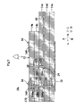
以下に、第1変形例に係るアンテナ素子10aについて図面を参照しながら説明する。図3は、アンテナ素子10aの断面図である。図3では、図1のA-Aに相当する位置のアンテナ素子10aの断面図を示した。
(First modification)
Hereinafter, the antenna element 10a according to the first modification will be described with reference to the drawings. FIG. 3 is a cross-sectional view of the antenna element 10a. FIG. 3 shows a cross-sectional view of the antenna element 10a at a position corresponding to AA in FIG.
アンテナ素子10aは、第1絶縁部材50を更に備えている点において、アンテナ素子10と相違する。第1絶縁部材50は、絶縁基材12の上に設けられている。第1絶縁部材50は、上下方向に見て、第1放射導体層20と重なっている。より詳細には、上下方向に見て、上端グランド導体層160により囲まれた領域と重なる部分には、絶縁体層14aが存在しない。そして、上端グランド導体層160により囲まれた領域と重なる部分には、絶縁体層14aの代わりに、第1絶縁部材50が設けられている。すなわち、絶縁基材12の上主面に凹部が設けられている。第1絶縁部材50は、凹部内に設けられている。第1絶縁部材50の誘電率は、絶縁基材12の誘電率より高い。なお、アンテナ素子10aのその他の構造は、アンテナ素子10bと同じであるので説明を省略する。
The antenna element 10a is different from the antenna element 10 in that the first insulating member 50 is further provided. The first insulating member 50 is provided on the insulating base material 12. The first insulating member 50 overlaps with the first radiating conductor layer 20 when viewed in the vertical direction. More specifically, when viewed in the vertical direction, the insulator layer 14a does not exist in the portion overlapping the region surrounded by the upper end ground conductor layer 160. A first insulating member 50 is provided in place of the insulator layer 14a in a portion overlapping the region surrounded by the upper end ground conductor layer 160. That is, a recess is provided on the upper main surface of the insulating base material 12. The first insulating member 50 is provided in the recess. The dielectric constant of the first insulating member 50 is higher than the dielectric constant of the insulating base material 12. Since the other structures of the antenna element 10a are the same as those of the antenna element 10b, the description thereof will be omitted.
アンテナ素子10aによれば、第1絶縁部材50の誘電率は、絶縁基材12の誘電率より高い。更に、第1絶縁部材50は、上下方向に見て、第1放射導体層20と重なっている。これにより、第1絶縁部材50が設けられたことによるパッチアンテナのアンテナ特性の広帯域化が図られる。
According to the antenna element 10a, the dielectric constant of the first insulating member 50 is higher than the dielectric constant of the insulating base material 12. Further, the first insulating member 50 overlaps with the first radiating conductor layer 20 when viewed in the vertical direction. As a result, the antenna characteristics of the patch antenna can be widened by providing the first insulating member 50.
(第2変形例)
以下に、第2変形例に係るアンテナ素子10bについて図面を参照しながら説明する。図4は、アンテナ素子10bの断面図である。図4では、図1のA-Aに相当する位置のアンテナ素子10bの断面図を示した。
(Second modification)
Hereinafter, the antenna element 10b according to the second modification will be described with reference to the drawings. FIG. 4 is a cross-sectional view of the antenna element 10b. FIG. 4 shows a cross-sectional view of the antenna element 10b at a position corresponding to AA in FIG.
アンテナ素子10bは、第1絶縁部材50の形状が異なる点及び第2絶縁部材52を更に備えている点において、アンテナ素子10aと相違する。第1絶縁部材50は、上下方向に見て、第1グランド導体16と重なっている。従って、第1絶縁部材50は、絶縁基材12の上主面の全面を覆っている。また、第2絶縁部材52は、第1絶縁部材50の上に設けられている。第2絶縁部材52は、第1絶縁部材50の上主面の全面を覆っている。第2絶縁部材52は、上下方向に見て、第1放射導体層20と重なっている。第2絶縁部材52の誘電率は、第1絶縁部材50の誘電率より高い。なお、アンテナ素子10bのその他の構造は、アンテナ素子10aと同じであるので説明を省略する。
The antenna element 10b is different from the antenna element 10a in that the shape of the first insulating member 50 is different and the second insulating member 52 is further provided. The first insulating member 50 overlaps with the first ground conductor 16 when viewed in the vertical direction. Therefore, the first insulating member 50 covers the entire surface of the upper main surface of the insulating base material 12. Further, the second insulating member 52 is provided on the first insulating member 50. The second insulating member 52 covers the entire surface of the upper main surface of the first insulating member 50. The second insulating member 52 overlaps with the first radiating conductor layer 20 when viewed in the vertical direction. The dielectric constant of the second insulating member 52 is higher than the dielectric constant of the first insulating member 50. Since the other structures of the antenna element 10b are the same as those of the antenna element 10a, the description thereof will be omitted.
アンテナ素子10aによれば、第1放射導体層20の上に設けられている第1絶縁部材50の誘電率及び第2絶縁部材52の誘電率は、上方向に行くにしたがって低下する。これにより、第1絶縁部材50及び第2絶縁部材52が設けられたことによるパッチアンテナの放射効率の低下がより抑制される。
According to the antenna element 10a, the dielectric constant of the first insulating member 50 provided on the first radiating conductor layer 20 and the dielectric constant of the second insulating member 52 decrease as they go upward. As a result, the decrease in radiation efficiency of the patch antenna due to the provision of the first insulating member 50 and the second insulating member 52 is further suppressed.
(第3変形例)
以下に、第3変形例に係るアンテナ素子10cについて図面を参照しながら説明する。図5は、アンテナ素子10cの断面図である。図5では、図1のA-Aに相当する位置のアンテナ素子10cの断面図を示した。
(Third modification example)
Hereinafter, the antenna element 10c according to the third modification will be described with reference to the drawings. FIG. 5 is a cross-sectional view of the antenna element 10c. FIG. 5 shows a cross-sectional view of the antenna element 10c at a position corresponding to AA in FIG.
アンテナ素子10cは、信号電極22の代わりに信号導体層60を備えている点、及び、層間接続導体v53,v54を備えていない点において、アンテナ素子10と相違する。
The antenna element 10c is different from the antenna element 10 in that it is provided with the signal conductor layer 60 instead of the signal electrode 22 and is not provided with the interlayer connection conductors v53 and v54.
信号導体層60は、絶縁体層14dの上主面に設けられている。信号導体層60は、層間接続導体v52の下端に接続されている。信号導体層60は、層間接続導体v52から右方向に延びている。信号導体層60には、第1放射導体層20が放射及び/又は受信する第1高周波信号が伝送される。
The signal conductor layer 60 is provided on the upper main surface of the insulator layer 14d. The signal conductor layer 60 is connected to the lower end of the interlayer connection conductor v52. The signal conductor layer 60 extends to the right from the interlayer connecting conductor v52. A first high frequency signal radiated and / or received by the first radiating conductor layer 20 is transmitted to the signal conductor layer 60.
なお、接続部172は、信号導体層60と干渉することを防止するために、信号導体層60の前又は後に設けられている。そのため、図5では、接続部172は図示されていない。アンテナ素子10cのその他の構造は、アンテナ素子10と同じであるので説明を省略する。
The connection portion 172 is provided before or after the signal conductor layer 60 in order to prevent it from interfering with the signal conductor layer 60. Therefore, in FIG. 5, the connection portion 172 is not shown. Since the other structures of the antenna element 10c are the same as those of the antenna element 10, the description thereof will be omitted.
また、絶縁基材12の右部は、絶縁体層14c~14eが積層された構造を有する。そのため、絶縁基材12の右部が可撓性を有する。従って、絶縁基材12の右部を折り曲げて使用することが可能である。
Further, the right portion of the insulating base material 12 has a structure in which the insulator layers 14c to 14e are laminated. Therefore, the right portion of the insulating base material 12 has flexibility. Therefore, the right portion of the insulating base material 12 can be bent and used.
以上のようなアンテナ素子10cでは、上下方向に見て、第1グランド導体16と第1放射導体層20との間には、第1高周波信号が伝送される信号導体層60、及び、グランド電位に接続される面状グランド導体層18が設けられている。ただし、上下方向に見て、第1グランド導体16と第1放射導体層20との間には、第1高周波信号が伝送される信号導体層60、及び、グランド電位に接続される面状グランド導体層18以外の導体は設けられていない。
In the antenna element 10c as described above, when viewed in the vertical direction, the signal conductor layer 60 in which the first high frequency signal is transmitted and the ground potential are between the first ground conductor 16 and the first radiation conductor layer 20. A planar ground conductor layer 18 connected to the ground conductor layer 18 is provided. However, when viewed in the vertical direction, between the first ground conductor 16 and the first radiation conductor layer 20, the signal conductor layer 60 through which the first high frequency signal is transmitted and the planar ground connected to the ground potential No conductor other than the conductor layer 18 is provided.
(第4変形例)
以下に、第4変形例に係るアンテナ素子10dについて図面を参照しながら説明する。図6は、アンテナ素子10dの分解斜視図である。
(Fourth modification)
Hereinafter, the antenna element 10d according to the fourth modification will be described with reference to the drawings. FIG. 6 is an exploded perspective view of the antenna element 10d.
アンテナ素子10dは、上端グランド導体層160の形状、及び、接続部170,174,176の有無において、アンテナ素子10と相違する。より詳細には、上端グランド導体層160は、上下方向に見て、長方形状を有している。上端グランド導体層160の長辺は、前後方向に延びている。上端グランド導体層160の短辺は、左右方向に延びている。上端グランド導体層160は、上下方向に見て、第1放射導体層20の右に位置している。
The antenna element 10d is different from the antenna element 10 in the shape of the upper end ground conductor layer 160 and the presence / absence of the connecting portions 170, 174, 176. More specifically, the upper end ground conductor layer 160 has a rectangular shape when viewed in the vertical direction. The long side of the upper end ground conductor layer 160 extends in the front-rear direction. The short side of the upper end ground conductor layer 160 extends in the left-right direction. The upper end ground conductor layer 160 is located to the right of the first radiating conductor layer 20 when viewed in the vertical direction.
上下方向に見て、第1放射導体層20から上端グランド導体層160に向かう方向を第1方向と定義する。本実施形態では、第1方向は、右方向である。上下方向に見て、第1方向に直交する方向を第2方向と定義する。本実施形態では、第2方向は、前後方向である。そして、第2方向における上端グランド導体層160の長さは、第2方向における第1放射導体層20の長さより長い。本実施形態では、前後方向における上端グランド導体層160の長さは、前後方向における第1放射導体層20の長さより長い。アンテナ素子10dのように、上下方向に見て、上端グランド導体層160は、第1放射導体層20から見て、一つの方向にのみに配置されていてもよい。
When viewed in the vertical direction, the direction from the first radiating conductor layer 20 toward the upper end ground conductor layer 160 is defined as the first direction. In this embodiment, the first direction is the right direction. The direction orthogonal to the first direction when viewed in the vertical direction is defined as the second direction. In this embodiment, the second direction is the front-back direction. The length of the upper end ground conductor layer 160 in the second direction is longer than the length of the first radiating conductor layer 20 in the second direction. In the present embodiment, the length of the upper end ground conductor layer 160 in the front-rear direction is longer than the length of the first radiation conductor layer 20 in the front-rear direction. Like the antenna element 10d, the upper end ground conductor layer 160 may be arranged in only one direction when viewed in the vertical direction from the first radiating conductor layer 20.
アンテナ素子10dによれば、上端グランド導体層160は、上下方向に見て、第1放射導体層20の右に位置している。前後方向における上端グランド導体層160の長さは、前後方向における第1放射導体層20の長さより長い。従って、第1放射導体層20が放射した高周波信号は、第1放射導体層20から右斜め上方向に進行することが上端グランド導体層160により阻害される。その結果、アンテナ素子10dによれば、パッチアンテナの指向性が向上する。
According to the antenna element 10d, the upper end ground conductor layer 160 is located to the right of the first radiating conductor layer 20 when viewed in the vertical direction. The length of the upper end ground conductor layer 160 in the front-rear direction is longer than the length of the first radiation conductor layer 20 in the front-rear direction. Therefore, the high-frequency signal radiated by the first radiating conductor layer 20 is prevented from traveling diagonally upward to the right from the first radiating conductor layer 20 by the upper end ground conductor layer 160. As a result, according to the antenna element 10d, the directivity of the patch antenna is improved.
(第5変形例)
以下に、第5変形例に係るアンテナ素子10eについて図面を参照しながら説明する。図7は、アンテナ素子10eの分解斜視図である。
(Fifth modification)
Hereinafter, the antenna element 10e according to the fifth modification will be described with reference to the drawings. FIG. 7 is an exploded perspective view of the antenna element 10e.
アンテナ素子10eは、第2グランド導体216を更に備えている点において、アンテナ素子10dと相違する。第2グランド導体216は、絶縁基材12に設けられている。より詳細には、第1グランド導体16及び第2グランド導体216は、上下方向に見て、第1放射導体層20から見て異なる方向に位置している。より詳細には、第1グランド導体16は、上下方向に見て、第1放射導体層20の右に位置している。第2グランド導体216は、上下方向に見て、第1放射導体層20の後に位置している。
The antenna element 10e is different from the antenna element 10d in that the second ground conductor 216 is further provided. The second ground conductor 216 is provided on the insulating base material 12. More specifically, the first ground conductor 16 and the second ground conductor 216 are located in different directions from the first radiation conductor layer 20 when viewed in the vertical direction. More specifically, the first ground conductor 16 is located to the right of the first radiation conductor layer 20 when viewed in the vertical direction. The second ground conductor 216 is located behind the first radiation conductor layer 20 when viewed in the vertical direction.
第2グランド導体216は、上端グランド導体層260、接続導体層286a~286c及び層間接続導体v216~v220を含んでいる。上端グランド導体層260は、上端グランド導体層260、接続導体層286a~286c及び層間接続導体v216~v220の内の最も上に位置する導体である。従って、上端グランド導体層260は、第2グランド導体216の上端を含んでいる。本実施形態では、上端グランド導体層260の上主面が第2グランド導体216の上端である。
The second ground conductor 216 includes an upper end ground conductor layer 260, connecting conductor layers 286a to 286c, and interlayer connecting conductors v216 to v220. The upper end ground conductor layer 260 is the uppermost conductor among the upper end ground conductor layer 260, the connecting conductor layers 286a to 286c, and the interlayer connecting conductors v216 to v220. Therefore, the upper end ground conductor layer 260 includes the upper end of the second ground conductor 216. In the present embodiment, the upper main surface of the upper end ground conductor layer 260 is the upper end of the second ground conductor 216.
上端グランド導体層260は、上下方向に見て、長方形状を有している。上端グランド導体層260の長辺は、左右方向に延びている。上端グランド導体層260の短辺は、前後方向に延びている。上端グランド導体層260は、上下方向に見て、第1放射導体層20の後に位置している。
The upper end ground conductor layer 260 has a rectangular shape when viewed in the vertical direction. The long side of the upper end ground conductor layer 260 extends in the left-right direction. The short side of the upper end ground conductor layer 260 extends in the front-rear direction. The upper end ground conductor layer 260 is located behind the first radiating conductor layer 20 when viewed in the vertical direction.
また、第2グランド導体216の上端である上端グランド導体層260は、絶縁体層14aの上主面に設けられている。一方、第1放射導体層20は、絶縁体層14bの上主面に設けられている。従って、第2グランド導体216の上端(上端グランド導体層260の上主面)は、第1放射導体層20より上に位置している。
Further, the upper end ground conductor layer 260, which is the upper end of the second ground conductor 216, is provided on the upper main surface of the insulator layer 14a. On the other hand, the first radiation conductor layer 20 is provided on the upper main surface of the insulator layer 14b. Therefore, the upper end of the second ground conductor 216 (the upper main surface of the upper end ground conductor layer 260) is located above the first radiation conductor layer 20.
層間接続導体v216~v220及び接続導体層286a~286cは、接続部276を形成している。接続部276は、絶縁基材12の後部に設けられている。また、接続部276は、上下方向に見て、第1放射導体層20の後に設けられている。接続部276は、面状グランド導体層18と上端グランド導体層260とを電気的に接続している。ただし、層間接続導体v216~v220及び接続導体層286a~286cの構造は、層間接続導体v16~v20及び接続導体層186a~186cの構造と同じであるので説明を省略する。これにより、第2グランド導体216は、グランド電位に接続されている。
The interlayer connecting conductors v216 to v220 and the connecting conductor layers 286a to 286c form a connecting portion 276. The connecting portion 276 is provided at the rear portion of the insulating base material 12. Further, the connecting portion 276 is provided after the first radiating conductor layer 20 when viewed in the vertical direction. The connecting portion 276 electrically connects the planar ground conductor layer 18 and the upper end ground conductor layer 260. However, since the structures of the interlayer connection conductors v216 to v220 and the connection conductor layers 286a to 286c are the same as the structures of the interlayer connection conductors v16 to v20 and the connection conductor layers 186a to 186c, the description thereof will be omitted. As a result, the second ground conductor 216 is connected to the ground potential.
以上のような第2グランド導体216は、上下方向に見て、第1放射導体層20から離れている。すなわち、第2グランド導体216は、上下方向に見て、第1放射導体層20と重なっていない。更に、上下方向に見て、第2グランド導体216と第1放射導体層20との間には、第1高周波信号が伝送される導体又はグランド電位に接続される導体以外の導体が設けられていない。本実施形態では、上下方向に見て、第1放射導体層20と第2グランド導体216との間には、面状グランド導体層18が存在し、その他の導体が存在しない。
The second ground conductor 216 as described above is separated from the first radiation conductor layer 20 when viewed in the vertical direction. That is, the second ground conductor 216 does not overlap with the first radiation conductor layer 20 when viewed in the vertical direction. Further, when viewed in the vertical direction, a conductor other than the conductor through which the first high frequency signal is transmitted or the conductor connected to the ground potential is provided between the second ground conductor 216 and the first radiation conductor layer 20. do not have. In the present embodiment, when viewed in the vertical direction, the planar ground conductor layer 18 exists between the first radiation conductor layer 20 and the second ground conductor 216, and no other conductors exist.
アンテナ素子10eによれば、第1グランド導体16及び第2グランド導体216は、上下方向に見て、第1放射導体層20から見て異なる方向に位置している。具体的には、第1グランド導体16は、上下方向に見て、第1放射導体層20の右に位置している。第2グランド導体216は、上下方向に見て、第1放射導体層20の後に位置している。これにより、第1放射導体層20が放射した高周波信号は、第1放射導体層20から右斜め上方向及び後斜め上方向に進行することが上端グランド導体層160,260により阻害される。その結果、アンテナ素子10eによれば、パッチアンテナの指向性が向上する。
According to the antenna element 10e, the first ground conductor 16 and the second ground conductor 216 are located in different directions from the first radiation conductor layer 20 when viewed in the vertical direction. Specifically, the first ground conductor 16 is located to the right of the first radiation conductor layer 20 when viewed in the vertical direction. The second ground conductor 216 is located behind the first radiation conductor layer 20 when viewed in the vertical direction. As a result, the high-frequency signal radiated by the first radiating conductor layer 20 is prevented from traveling diagonally upward to the right and diagonally upward to the rear by the upper end ground conductor layers 160 and 260 from the first radiating conductor layer 20. As a result, according to the antenna element 10e, the directivity of the patch antenna is improved.
(第6変形例)
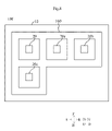
以下に、第6変形例に係るアンテナ素子10fについて図面を参照しながら説明する。図8は、アンテナ素子10fの第1放射導体層20、第2放射導体層20a~第4放射導体層20c及び上端グランド導体層160の上面図である。
(6th modification)
Hereinafter, the antenna element 10f according to the sixth modification will be described with reference to the drawings. FIG. 8 is a top view of the first radiant conductor layer 20, the second radiant conductor layer 20a to the fourth radiant conductor layer 20c, and the upper end ground conductor layer 160 of the antenna element 10f.
アンテナ素子10fは、第2放射導体層20a~第4放射導体層20cの有無及び上端グランド導体層160の形状において、アンテナ素子10と相違する。アンテナ素子10fは、第2放射導体層20a~第4放射導体層20cを更に備えている。
The antenna element 10f is different from the antenna element 10 in the presence / absence of the second radiating conductor layer 20a to the fourth radiating conductor layer 20c and the shape of the upper end ground conductor layer 160. The antenna element 10f further includes a second radiating conductor layer 20a to a fourth radiating conductor layer 20c.
第2放射導体層20a~第4放射導体層20cのそれぞれは、第2高周波信号ないし第4高周波信号を放射及び/又は受信する。第2放射導体層20a~第4放射導体層20cは、絶縁基材12に設けられている。本実施形態では、第2放射導体層20a~第4放射導体層20cは、絶縁体層14bの上主面に設けられている。そのため、第2放射導体層20a~第4放射導体層20cは、面状グランド導体層18(第2面状グランド導体層 図8では図示せず)の上に位置している。これにより、第2放射導体層20a~第4放射導体層20cの下主面は、上下方向に見て、面状グランド導体層18(第2面状グランド導体層)の上主面と重なっている。
Each of the second radiation conductor layer 20a to the fourth radiation conductor layer 20c radiates and / or receives a second high frequency signal or a fourth high frequency signal. The second radiating conductor layer 20a to the fourth radiating conductor layer 20c are provided on the insulating base material 12. In the present embodiment, the second radiating conductor layer 20a to the fourth radiating conductor layer 20c are provided on the upper main surface of the insulator layer 14b. Therefore, the second radiating conductor layer 20a to the fourth radiating conductor layer 20c are located on the planar ground conductor layer 18 (the second planar ground conductor layer (not shown in FIG. 8)). As a result, the lower main surface of the second radiant conductor layer 20a to the fourth radiant conductor layer 20c overlaps with the upper main surface of the planar ground conductor layer 18 (second planar ground conductor layer) when viewed in the vertical direction. There is.
また、第1放射導体層20、第2放射導体層20a及び第3放射導体層20bは、上下方向に見て、左から右へとこの順に一列に並んでいる。第4放射導体層20cは、上下方向に見て、第1放射導体層20の後に位置している。
Further, the first radiant conductor layer 20, the second radiant conductor layer 20a, and the third radiant conductor layer 20b are arranged in a row in this order from left to right when viewed in the vertical direction. The fourth radiant conductor layer 20c is located behind the first radiant conductor layer 20 when viewed in the vertical direction.
上端グランド導体層160は、上下方向に見て、第1放射導体層20、第2放射導体層20a~第4放射導体層20cのそれぞれの周囲を囲む複数の環形状が組み合わされた形状を有している。従って、上端グランド導体層160(第1グランド導体16)は、上下方向に見て、第1放射導体層20と第2放射導体層20aとの間に存在している。上端グランド導体層160(第1グランド導体16)は、上下方向に見て、第2放射導体層20aと第3放射導体層20bとの間に存在している。上端グランド導体層160(第1グランド導体16)は、上下方向に見て、第1放射導体層20と第4放射導体層20cとの間に存在している。これにより、隣り合う第1放射導体層20、第2放射導体層20a~第4放射導体層20c間のアイソレーションを向上させることができる。
The upper end ground conductor layer 160 has a shape in which a plurality of ring shapes surrounding each of the first radiant conductor layer 20 and the second radiant conductor layer 20a to the fourth radiant conductor layer 20c are combined when viewed in the vertical direction. is doing. Therefore, the upper end ground conductor layer 160 (first ground conductor 16) exists between the first radiant conductor layer 20 and the second radiant conductor layer 20a when viewed in the vertical direction. The upper end ground conductor layer 160 (first ground conductor 16) exists between the second radiant conductor layer 20a and the third radiant conductor layer 20b when viewed in the vertical direction. The upper end ground conductor layer 160 (first ground conductor 16) exists between the first radiant conductor layer 20 and the fourth radiant conductor layer 20c when viewed in the vertical direction. Thereby, the isolation between the adjacent first radiating conductor layer 20 and the second radiating conductor layer 20a to the fourth radiating conductor layer 20c can be improved.
また、上端グランド導体層160は、絶縁体層14aの上主面に設けられている。第1放射導体層20及び第2放射導体層20a~第4放射導体層20cは、絶縁体層14bの上主面に設けられている。従って、第1グランド導体16の上端(上端グランド導体層160の上主面)は、第1放射導体層20及び第2放射導体層20a~第4放射導体層20cより上に位置している。
Further, the upper end ground conductor layer 160 is provided on the upper main surface of the insulator layer 14a. The first radiant conductor layer 20 and the second radiant conductor layer 20a to the fourth radiant conductor layer 20c are provided on the upper main surface of the insulator layer 14b. Therefore, the upper end of the first ground conductor 16 (the upper main surface of the upper end ground conductor layer 160) is located above the first radiation conductor layer 20 and the second radiation conductor layer 20a to the fourth radiation conductor layer 20c.
また、第1グランド導体16は、上下方向に見て、第1放射導体層20及び第2放射導体層20a~第4放射導体層20cから離れている。そして、上下方向に見て、第1グランド導体16と第1放射導体層20との間には、第1高周波信号が伝送される導体又はグランド電位に接続される導体以外の導体が設けられていない。上下方向に見て、第1グランド導体16と第2放射導体層20aとの間には、第2高周波信号が伝送される導体又はグランド電位に接続される導体以外の導体が設けられていない。上下方向に見て、第1グランド導体16と第3放射導体層20bとの間には、第3高周波信号が伝送される導体又はグランド電位に接続される導体以外の導体が設けられていない。上下方向に見て、第1グランド導体16と第4放射導体層20cとの間には、第4高周波信号が伝送される導体又はグランド電位に接続される導体以外の導体が設けられていない。
Further, the first ground conductor 16 is separated from the first radiant conductor layer 20 and the second radiant conductor layer 20a to the fourth radiant conductor layer 20c when viewed in the vertical direction. When viewed in the vertical direction, a conductor other than the conductor through which the first high frequency signal is transmitted or the conductor connected to the ground potential is provided between the first ground conductor 16 and the first radiation conductor layer 20. do not have. When viewed in the vertical direction, no conductor other than the conductor through which the second high frequency signal is transmitted or the conductor connected to the ground potential is provided between the first ground conductor 16 and the second radiation conductor layer 20a. When viewed in the vertical direction, no conductor other than the conductor through which the third high frequency signal is transmitted or the conductor connected to the ground potential is provided between the first ground conductor 16 and the third radiating conductor layer 20b. When viewed in the vertical direction, no conductor other than the conductor through which the fourth high frequency signal is transmitted or the conductor connected to the ground potential is provided between the first ground conductor 16 and the fourth radiation conductor layer 20c.
(第7変形例)
以下に、第7変形例に係るアンテナ素子10gについて図面を参照しながら説明する。図9は、アンテナ素子10gの第1放射導体層20、第2放射導体層20a~第4放射導体層20c及び上端グランド導体層160の上面図である。
(7th modification)
Hereinafter, the antenna element 10g according to the seventh modification will be described with reference to the drawings. FIG. 9 is a top view of the first radiating conductor layer 20, the second radiating conductor layer 20a to the fourth radiating conductor layer 20c, and the upper end ground conductor layer 160 of the antenna element 10g.
アンテナ素子10gは、上端グランド導体層160の形状において、アンテナ素子10fと相違する。より詳細には、上端グランド導体層160は、上下方向に見て、第1放射導体層20の左及び前には存在しない。上端グランド導体層160は、上下方向に見て、第2放射導体層20aの前には存在しない。上端グランド導体層160は、上下方向に見て、第3放射導体層20bの前には存在しない。上端グランド導体層160は、上下方向に見て、第4放射導体層20cの左及び後には存在しない。
The antenna element 10g is different from the antenna element 10f in the shape of the upper end ground conductor layer 160. More specifically, the upper end ground conductor layer 160 does not exist to the left or in front of the first radiation conductor layer 20 when viewed in the vertical direction. The upper end ground conductor layer 160 does not exist in front of the second radiating conductor layer 20a when viewed in the vertical direction. The upper end ground conductor layer 160 does not exist in front of the third radiating conductor layer 20b when viewed in the vertical direction. The upper end ground conductor layer 160 does not exist to the left and behind the fourth radiating conductor layer 20c when viewed in the vertical direction.
以上のように、上端グランド導体層160は、上下方向に見て、第1放射導体層20及び第2放射導体層20a~第4放射導体層20cのそれぞれの周囲を囲む複数の環形状が組み合わされた形状を有していなくてもよい。ただし、アンテナ素子10gでは、上端グランド導体層160は、以下に説明する構造を有している。上下方向に見て、第1放射導体層20を中心として時計回り方向における上端グランド導体層160の上流端tuと第1放射導体層20とを接続する直線を第1直線L1と定義する。上下方向に見て、第1放射導体層20を中心として時計回り方向における上端グランド導体層160の下流端tdと第1放射導体層20とを接続する直線を第2直線L2と定義する。このとき、第1直線L1と第2直線L2とがなす角度θは、180度以上である。角度θは、第1直線L1と第2直線L2とがなす角度の内の第1直線L1、第2直線L2及び上端グランド導体層160により囲まれた領域内に位置する角度である。従って、上端グランド導体層160は、上下方向に見て、第1放射導体層20の周囲の半分以上に存在している。説明を省略するが、上端グランド導体層160は、上下方向に見て、第2放射導体層20a~第4放射導体層20cのそれぞれの周囲の半分以上に存在している。これにより、アンテナ素子10において、第1放射導体層20及び第2放射導体層20a~第4放射導体層20cの指向性を向上させることができる。
As described above, the upper end ground conductor layer 160 is a combination of a plurality of ring shapes surrounding each of the first radiation conductor layer 20 and the second radiation conductor layer 20a to the fourth radiation conductor layer 20c when viewed in the vertical direction. It does not have to have a shaped shape. However, in the antenna element 10g, the upper end ground conductor layer 160 has the structure described below. When viewed in the vertical direction, the straight line connecting the upstream end tu of the upper end ground conductor layer 160 and the first radiating conductor layer 20 in the clockwise direction with the first radiating conductor layer 20 as the center is defined as the first straight line L1. When viewed in the vertical direction, the straight line connecting the downstream end td of the upper end ground conductor layer 160 in the clockwise direction with the first radiating conductor layer 20 as the center and the first radiating conductor layer 20 is defined as the second straight line L2. At this time, the angle θ formed by the first straight line L1 and the second straight line L2 is 180 degrees or more. The angle θ is an angle located in the region surrounded by the first straight line L1, the second straight line L2, and the upper end ground conductor layer 160 among the angles formed by the first straight line L1 and the second straight line L2. Therefore, the upper end ground conductor layer 160 exists in more than half of the periphery of the first radiating conductor layer 20 when viewed in the vertical direction. Although the description is omitted, the upper end ground conductor layer 160 exists in more than half of each of the second radiant conductor layer 20a to the fourth radiant conductor layer 20c when viewed in the vertical direction. Thereby, in the antenna element 10, the directivity of the first radiating conductor layer 20 and the second radiating conductor layer 20a to the fourth radiating conductor layer 20c can be improved.
なお、第1直線L1及び第2直線L2の端は、上下方向に見て、第1放射導体層20の重心に位置している。
The ends of the first straight line L1 and the second straight line L2 are located at the center of gravity of the first radiation conductor layer 20 when viewed in the vertical direction.
(第8変形例)
以下に、第8変形例に係るアンテナ素子10hについて図面を参照しながら説明する。
(8th modification)
Hereinafter, the antenna element 10h according to the eighth modification will be described with reference to the drawings.
図10は、アンテナ素子10hの断面図である。図10では、図1のA-Aに相当する位置のアンテナ素子10hの断面図を示した。
FIG. 10 is a cross-sectional view of the antenna element 10h. FIG. 10 shows a cross-sectional view of the antenna element 10h at a position corresponding to AA in FIG.
アンテナ素子10hは、第1放射導体層20が絶縁体層14aの上主面に設けられている点において、アンテナ素子10と相違する。より詳細には、絶縁体層14a~14eは、第1絶縁体層である絶縁体層14aを含んでいる。上端グランド導体層160と第1放射導体層20とは、絶縁体層14a(第1絶縁体層)に設けられている。本実施形態では、上端グランド導体層160と第1放射導体層20とは、絶縁体層14a(第1絶縁体層)の上主面に設けられている。
The antenna element 10h is different from the antenna element 10 in that the first radiation conductor layer 20 is provided on the upper main surface of the insulator layer 14a. More specifically, the insulator layers 14a to 14e include an insulator layer 14a which is a first insulator layer. The upper end ground conductor layer 160 and the first radiating conductor layer 20 are provided on the insulator layer 14a (first insulator layer). In the present embodiment, the upper end ground conductor layer 160 and the first radiation conductor layer 20 are provided on the upper main surface of the insulator layer 14a (first insulator layer).
ここで、絶縁基材12において、第1グランド導体16が設けられている領域を領域A2,A3と定義する。また、絶縁基材12において、第1放射導体層20が設けられている領域を領域A1と定義する。アンテナ素子10hの製造時には、領域A1に加わる圧力が領域A2,A3に加わる圧力より大きくなるように、絶縁基材12に圧着を行う。これにより、絶縁基材12の圧着工程において、領域A1が領域A2,A3より大きく圧縮される。その結果、絶縁体層14aは、上下方向に曲がっている。具体的には、領域A1における絶縁体層14aは、領域A2,A3における絶縁体層14aより下に位置している。これにより、上端グランド導体層160の上端が第1放射導体層20より上に位置するように、絶縁体層14a(第1絶縁体層)は上下方向に曲がっている。また、絶縁体層14a(第1絶縁体層)が上下方向に曲がることにより、上端グランド導体層160が上下方向に曲がっている。換言すると、絶縁体層14a(第1絶縁体層)が上下方向に曲がっている形状に沿って、上端グランド導体層160が上下方向に曲がっている。これにより、第1放射導体層20の左右方向に層間接続導体に加えて上端グランド導体層160が存在するようになる。その結果、アンテナ素子10hの指向性を向上させることができる。また、アンテナ素子10hが複数の放射導体層を含む場合には、隣り合う複数の放射導体層間のアイソレーションを向上させることができる。
Here, in the insulating base material 12, the regions where the first ground conductor 16 is provided are defined as regions A2 and A3. Further, in the insulating base material 12, the region where the first radiation conductor layer 20 is provided is defined as the region A1. At the time of manufacturing the antenna element 10h, the insulating base material 12 is crimped so that the pressure applied to the regions A1 is larger than the pressure applied to the regions A2 and A3. As a result, in the crimping step of the insulating base material 12, the region A1 is compressed more than the regions A2 and A3. As a result, the insulator layer 14a is bent in the vertical direction. Specifically, the insulator layer 14a in the region A1 is located below the insulator layer 14a in the regions A2 and A3. As a result, the insulator layer 14a (first insulator layer) is bent in the vertical direction so that the upper end of the upper end ground conductor layer 160 is located above the first radiation conductor layer 20. Further, the insulator layer 14a (first insulator layer) is bent in the vertical direction, so that the upper end ground conductor layer 160 is bent in the vertical direction. In other words, the upper end ground conductor layer 160 is bent in the vertical direction along the shape in which the insulator layer 14a (first insulator layer) is bent in the vertical direction. As a result, the upper end ground conductor layer 160 is present in the left-right direction of the first radiation conductor layer 20 in addition to the interlayer connecting conductor. As a result, the directivity of the antenna element 10h can be improved. Further, when the antenna element 10h includes a plurality of radiation conductor layers, the isolation between the plurality of adjacent radiation conductor layers can be improved.
また、アンテナ素子10hは、レジスト層54、接着層56及び樹脂層58を更に備えている。レジスト層54、接着層56及び樹脂層58は、絶縁基材12の上に下から上へとこの順に積層されている。レジスト層54の誘電率は、絶縁基材12の誘電率より高い。接着層56の誘電率は、レジスト層54の誘電率より高い。樹脂層58の誘電率は、接着層56の誘電率より高い。
Further, the antenna element 10h further includes a resist layer 54, an adhesive layer 56, and a resin layer 58. The resist layer 54, the adhesive layer 56, and the resin layer 58 are laminated on the insulating base material 12 from bottom to top in this order. The dielectric constant of the resist layer 54 is higher than the dielectric constant of the insulating base material 12. The dielectric constant of the adhesive layer 56 is higher than the dielectric constant of the resist layer 54. The dielectric constant of the resin layer 58 is higher than the dielectric constant of the adhesive layer 56.
アンテナ素子10hのように、絶縁基材12の変形を利用して、上端グランド導体層160の上端を第1放射導体層20より上に位置させてもよい。
Like the antenna element 10h, the upper end of the upper end ground conductor layer 160 may be positioned above the first radiation conductor layer 20 by utilizing the deformation of the insulating base material 12.
(その他の実施形態)
本発明に係るアンテナ素子は、アンテナ素子10,10a~10hに限らず、その要旨の範囲内において変更可能である。また、アンテナ素子10,10a~10hの構造を任意に組み合わせてもよい。
(Other embodiments)
The antenna element according to the present invention is not limited to the antenna elements 10, 10a to 10h, and can be changed within the scope of the gist thereof. Further, the structures of the antenna elements 10, 10a to 10h may be arbitrarily combined.
なお、アンテナ素子10,10a~10hにおいて、第1グランド導体16の上端は、上端グランド導体層160の上面である。しかしながら、上端グランド導体層160の上に層間接続導体が更に設けられる場合がある。このような場合には、第1グランド導体16の上端は、層間接続導体の上端である。このように、第1グランド導体16の上端は、上端グランド導体層160以外の構成の上端であってもよい。また、アンテナ素子10hのように上端グランド導体層160が上下方向に曲がっている場合がある。この場合には、第1グランド導体16の上端は、上端グランド導体層160の上主面の内の最も上に位置する部分である。
In the antenna elements 10, 10a to 10h, the upper end of the first ground conductor 16 is the upper surface of the upper end ground conductor layer 160. However, an interlayer connecting conductor may be further provided on the upper end ground conductor layer 160. In such a case, the upper end of the first ground conductor 16 is the upper end of the interlayer connecting conductor. As described above, the upper end of the first ground conductor 16 may be the upper end of the configuration other than the upper end ground conductor layer 160. Further, the upper end ground conductor layer 160 may be bent in the vertical direction as in the antenna element 10h. In this case, the upper end of the first ground conductor 16 is the uppermost portion of the upper main surface of the upper end ground conductor layer 160.
なお、アンテナ素子10,10a~10c,10f,10hにおいて、上端グランド導体層160は、上下方向に見て、環形状を有していなくてもよい。
In the antenna elements 10, 10a to 10c, 10f, 10h, the upper end ground conductor layer 160 does not have to have a ring shape when viewed in the vertical direction.
なお、アンテナ素子10d,10eにおいて、前後方向における上端グランド導体層160の長さは、前後方向における第1放射導体層20の長さ以下であってもよい。
In the antenna elements 10d and 10e, the length of the upper end ground conductor layer 160 in the front-rear direction may be less than or equal to the length of the first radiation conductor layer 20 in the front-rear direction.
なお、アンテナ素子10gにおいて、第1直線L1と第2直線L2とがなす角度θは、180度より小さくてもよい。
In the antenna element 10g, the angle θ formed by the first straight line L1 and the second straight line L2 may be smaller than 180 degrees.
なお、アンテナ素子10f,10gにおいて、第1グランド導体16は、上下方向に見て、第1放射導体層20と第2放射導体層20aとの間に位置していなくてもよい。
In the antenna elements 10f and 10g, the first ground conductor 16 does not have to be located between the first radiating conductor layer 20 and the second radiating conductor layer 20a when viewed in the vertical direction.
なお、アンテナ素子10eにおいて、例えば、上端グランド導体層160は、上下方向に見て、第1放射導体層20の右に位置し、上端グランド導体層260は、上下方向に見て、第1放射導体層20の左に位置していてもよい。
In the antenna element 10e, for example, the upper end ground conductor layer 160 is located to the right of the first radiation conductor layer 20 when viewed in the vertical direction, and the upper end ground conductor layer 260 is the first radiation when viewed in the vertical direction. It may be located to the left of the conductor layer 20.
なお、アンテナ素子10a,10bにおいて、第1絶縁部材50の誘電率は、絶縁基材12の誘電率以下であってもよい。また、アンテナ素子10bにおいて、第2絶縁部材52の誘電率は、第1絶縁部材50の誘電率以下であってもよい。
In the antenna elements 10a and 10b, the dielectric constant of the first insulating member 50 may be equal to or less than the dielectric constant of the insulating base material 12. Further, in the antenna element 10b, the dielectric constant of the second insulating member 52 may be equal to or less than the dielectric constant of the first insulating member 50.
なお、アンテナ素子10fは、面状グランド導体層18に加えて、第2面状グランド導体層を更に備えていてもよい。この場合、第1放射導体層20の下主面は、上下方向に見て、面状グランド導体層18の上主面と重なっている。第2放射導体層20a~第4放射導体層20cの下主面は、上下方向に見て、第2面状グランド導体層の上主面と重なっている。すなわち、第1面状グランド導体層と第2面状グランド導体層とは、1個の面状グランド導体層であってもよいし、2個の面状グランド導体層であってもよい。
The antenna element 10f may further include a second planar ground conductor layer in addition to the planar ground conductor layer 18. In this case, the lower main surface of the first radiating conductor layer 20 overlaps with the upper main surface of the planar ground conductor layer 18 when viewed in the vertical direction. The lower main surface of the second radiant conductor layer 20a to the fourth radiant conductor layer 20c overlaps the upper main surface of the second planar ground conductor layer when viewed in the vertical direction. That is, the first planar ground conductor layer and the second planar ground conductor layer may be one planar ground conductor layer or two planar ground conductor layers.