WO2022064798A1 - Inspection device - Google Patents

Inspection device Download PDF

Info

Publication number
WO2022064798A1
WO2022064798A1 PCT/JP2021/024153 JP2021024153W WO2022064798A1 WO 2022064798 A1 WO2022064798 A1 WO 2022064798A1 JP 2021024153 W JP2021024153 W JP 2021024153W WO 2022064798 A1 WO2022064798 A1 WO 2022064798A1
Authority
WO
WIPO (PCT)
Prior art keywords
light
optical amplifier
optical
photodetector
input
Prior art date
Application number
PCT/JP2021/024153
Other languages
French (fr)
Japanese (ja)
Inventor
共則 中村
哲人 内角
充哲 西沢
Original Assignee
浜松ホトニクス株式会社
Priority date (The priority date is an assumption and is not a legal conclusion. Google has not performed a legal analysis and makes no representation as to the accuracy of the date listed.)
Filing date
Publication date
Application filed by 浜松ホトニクス株式会社 filed Critical 浜松ホトニクス株式会社
Priority to KR1020227043070A priority Critical patent/KR20230070410A/en
Priority to US18/020,273 priority patent/US20240012047A1/en
Priority to EP21871930.0A priority patent/EP4213189A1/en
Priority to CN202180064713.2A priority patent/CN116195042A/en
Priority to JP2022551149A priority patent/JPWO2022064798A1/ja
Publication of WO2022064798A1 publication Critical patent/WO2022064798A1/en

Links

Images

Classifications

    • GPHYSICS
    • G01MEASURING; TESTING
    • G01RMEASURING ELECTRIC VARIABLES; MEASURING MAGNETIC VARIABLES
    • G01R31/00Arrangements for testing electric properties; Arrangements for locating electric faults; Arrangements for electrical testing characterised by what is being tested not provided for elsewhere
    • G01R31/28Testing of electronic circuits, e.g. by signal tracer
    • G01R31/302Contactless testing
    • G01R31/308Contactless testing using non-ionising electromagnetic radiation, e.g. optical radiation
    • G01R31/311Contactless testing using non-ionising electromagnetic radiation, e.g. optical radiation of integrated circuits
    • GPHYSICS
    • G01MEASURING; TESTING
    • G01JMEASUREMENT OF INTENSITY, VELOCITY, SPECTRAL CONTENT, POLARISATION, PHASE OR PULSE CHARACTERISTICS OF INFRARED, VISIBLE OR ULTRAVIOLET LIGHT; COLORIMETRY; RADIATION PYROMETRY
    • G01J1/00Photometry, e.g. photographic exposure meter
    • G01J1/42Photometry, e.g. photographic exposure meter using electric radiation detectors
    • GPHYSICS
    • G01MEASURING; TESTING
    • G01RMEASURING ELECTRIC VARIABLES; MEASURING MAGNETIC VARIABLES
    • G01R31/00Arrangements for testing electric properties; Arrangements for locating electric faults; Arrangements for electrical testing characterised by what is being tested not provided for elsewhere
    • G01R31/28Testing of electronic circuits, e.g. by signal tracer
    • G01R31/317Testing of digital circuits
    • G01R31/31708Analysis of signal quality
    • G01R31/31709Jitter measurements; Jitter generators
    • HELECTRICITY
    • H01ELECTRIC ELEMENTS
    • H01LSEMICONDUCTOR DEVICES NOT COVERED BY CLASS H10
    • H01L31/00Semiconductor devices sensitive to infrared radiation, light, electromagnetic radiation of shorter wavelength or corpuscular radiation and specially adapted either for the conversion of the energy of such radiation into electrical energy or for the control of electrical energy by such radiation; Processes or apparatus specially adapted for the manufacture or treatment thereof or of parts thereof; Details thereof
    • H01L31/08Semiconductor devices sensitive to infrared radiation, light, electromagnetic radiation of shorter wavelength or corpuscular radiation and specially adapted either for the conversion of the energy of such radiation into electrical energy or for the control of electrical energy by such radiation; Processes or apparatus specially adapted for the manufacture or treatment thereof or of parts thereof; Details thereof in which radiation controls flow of current through the device, e.g. photoresistors
    • H01L31/10Semiconductor devices sensitive to infrared radiation, light, electromagnetic radiation of shorter wavelength or corpuscular radiation and specially adapted either for the conversion of the energy of such radiation into electrical energy or for the control of electrical energy by such radiation; Processes or apparatus specially adapted for the manufacture or treatment thereof or of parts thereof; Details thereof in which radiation controls flow of current through the device, e.g. photoresistors characterised by at least one potential-jump barrier or surface barrier, e.g. phototransistors
    • H01L31/101Devices sensitive to infrared, visible or ultraviolet radiation
    • H01L31/102Devices sensitive to infrared, visible or ultraviolet radiation characterised by only one potential barrier or surface barrier
    • H01L31/105Devices sensitive to infrared, visible or ultraviolet radiation characterised by only one potential barrier or surface barrier the potential barrier being of the PIN type
    • HELECTRICITY
    • H01ELECTRIC ELEMENTS
    • H01SDEVICES USING THE PROCESS OF LIGHT AMPLIFICATION BY STIMULATED EMISSION OF RADIATION [LASER] TO AMPLIFY OR GENERATE LIGHT; DEVICES USING STIMULATED EMISSION OF ELECTROMAGNETIC RADIATION IN WAVE RANGES OTHER THAN OPTICAL
    • H01S5/00Semiconductor lasers
    • H01S5/005Optical components external to the laser cavity, specially adapted therefor, e.g. for homogenisation or merging of the beams or for manipulating laser pulses, e.g. pulse shaping
    • H01S5/0085Optical components external to the laser cavity, specially adapted therefor, e.g. for homogenisation or merging of the beams or for manipulating laser pulses, e.g. pulse shaping for modulating the output, i.e. the laser beam is modulated outside the laser cavity
    • HELECTRICITY
    • H01ELECTRIC ELEMENTS
    • H01LSEMICONDUCTOR DEVICES NOT COVERED BY CLASS H10
    • H01L22/00Testing or measuring during manufacture or treatment; Reliability measurements, i.e. testing of parts without further processing to modify the parts as such; Structural arrangements therefor
    • H01L22/10Measuring as part of the manufacturing process
    • H01L22/12Measuring as part of the manufacturing process for structural parameters, e.g. thickness, line width, refractive index, temperature, warp, bond strength, defects, optical inspection, electrical measurement of structural dimensions, metallurgic measurement of diffusions

Abstract

This inspection device comprises: a light source that emits light; an optical amplifier that amplifies the inputted light and outputs the resultant light; an optical system (an objective lens, an image-forming optical system, and a scan optical system) that irradiates a semiconductor device with the light from the light source and guides the light from the semiconductor device to the optical amplifier; and an optical detector that detects the light outputted from the optical amplifier. The optical amplifier amplifies the inputted light so as not to be saturated.

Description

検査装置Inspection equipment
 本発明の一態様は、検査装置に関する。 One aspect of the present invention relates to an inspection device.
 駆動している半導体デバイスに対してレーザ光を照射し、その反射光の強度変調を検出することによって、該半導体デバイスの故障解析を行う検査装置が知られている(例えば特許文献1参照)。 There is known an inspection device that analyzes a failure of a semiconductor device by irradiating the driven semiconductor device with a laser beam and detecting the intensity modulation of the reflected light (see, for example, Patent Document 1).
特開2007-64975号公報JP-A-2007-64975
 近年、半導体デバイスの性能向上に伴って、より高い周波数帯域を含む広帯域の現象を検出することができる検査装置が求められている。具体的には、例えば、10psを下回る速度でスイッチングをしているトランジスタにおける微小なジッダ(例えば10ps程度のジッダ)を正確に検出することができる検査装置が求められている。 In recent years, with the improvement of the performance of semiconductor devices, there is a demand for an inspection device capable of detecting a wide band phenomenon including a higher frequency band. Specifically, for example, there is a demand for an inspection device capable of accurately detecting a minute jigdah (for example, a jigdah of about 10 ps) in a transistor switching at a speed of less than 10 ps.
 本発明の一態様は上記実情に鑑みてなされたものであり、広帯域の現象を正確に検出することが可能な検査装置を提供することを目的とする。 One aspect of the present invention has been made in view of the above circumstances, and an object of the present invention is to provide an inspection device capable of accurately detecting a wideband phenomenon.
 本発明の一態様に係る検査装置は、光を発生する光源と、入力された光を増幅して出力する光増幅器と、光源からの光を半導体デバイスに照射し、該半導体デバイスからの光を光増幅器に導光する光学系と、光増幅器から出力された光を検出する光検出器と、を備え、光増幅器は、入力された光を飽和しないように増幅する。 The inspection device according to one aspect of the present invention irradiates a semiconductor device with a light source that generates light, an optical amplifier that amplifies and outputs the input light, and light from the light source, and emits light from the semiconductor device. It includes an optical system that guides the light to the optical amplifier and an optical detector that detects the light output from the optical amplifier, and the optical amplifier amplifies the input light so as not to saturate it.
 本発明の一態様に係る検査装置では、半導体デバイスからの光が光増幅器に入力され、該光増幅器において飽和しない範囲で光が増幅されて出力され、光増幅器から出力された光が光検出器において検出される。通常、半導体デバイスに照射される光の光量は、半導体デバイスが破壊されない程度に小さくされる。このため、半導体デバイスからの戻り光の光量も小さくなるが、戻り光の光量が小さい場合には検出系のノイズ(サーマルノイズ)の影響によって検出精度が低下するおそれがある。このことから、従来、光検出器として、戻り光を増幅する増倍層を有する光検出器が用いられている。しかしながら、増倍層を有する光検出器については、容量が比較的大きくなるため、高速な信号の計測(高い周波数帯域の現象の検出)に向かない。この点、本発明の一態様に係る検査装置では、上述したように、光検出器とは別に光増幅器が設けられており、該光増幅器において増幅された光が光検出器において検出されるため、検出精度を担保するための信号の増幅については光増幅器によって行い、増幅後の光の検出を光検出器によって行うことが可能になる。このような構成においては、光検出器として、増倍層を有さず比較的容量が小さい光検出器を用いることができるため、高い周波数帯域の現象を検出することができる。また、本発明の一態様に係る検査装置では、光増幅器によって、飽和しない範囲で光が増幅されている。飽和する場合には、入力光に含まれる微小信号が増幅後において消えてしまい、微小信号が適切に検出されないおそれがある。この点、飽和しない範囲で光が増幅されることにより、微小信号を含んだ出力光に基づき、微小な現象についても正確に検出することができる。以上のように、本発明の一態様に係る検査装置によれば、高い周波数帯域を含む広帯域の現象を正確に検出することができる。 In the inspection apparatus according to one aspect of the present invention, light from a semiconductor device is input to an optical amplifier, the light is amplified and output within a range that does not saturate in the optical amplifier, and the light output from the optical amplifier is a photodetector. Detected in. Normally, the amount of light emitted to a semiconductor device is reduced to such an extent that the semiconductor device is not destroyed. Therefore, the amount of return light from the semiconductor device is also small, but if the amount of return light is small, the detection accuracy may decrease due to the influence of noise (thermal noise) of the detection system. For this reason, conventionally, as a photodetector, a photodetector having a multiplying layer that amplifies the return light has been used. However, a photodetector having a multiplier layer has a relatively large capacitance, and is not suitable for high-speed signal measurement (detection of a phenomenon in a high frequency band). In this respect, in the inspection device according to one aspect of the present invention, as described above, an optical amplifier is provided separately from the photodetector, and the light amplified by the photodetector is detected by the photodetector. The signal amplification for ensuring the detection accuracy is performed by an optical amplifier, and the light after amplification can be detected by a photodetector. In such a configuration, as the photodetector, a photodetector having a relatively small capacity without a multiplying layer can be used, so that a phenomenon in a high frequency band can be detected. Further, in the inspection device according to one aspect of the present invention, light is amplified in a non-saturated range by an optical amplifier. When saturated, the minute signal contained in the input light disappears after amplification, and the minute signal may not be detected properly. In this respect, by amplifying the light in a non-saturating range, it is possible to accurately detect even a minute phenomenon based on the output light including a minute signal. As described above, according to the inspection apparatus according to one aspect of the present invention, it is possible to accurately detect a wideband phenomenon including a high frequency band.
 光増幅器は、入力された光の光量に対する出力する光の光量の変化が線形になるように、入力された光を増幅してもよい。このように、入力光と出力光とが線形の関係にあることによって、半導体デバイスからの戻り光に係る現象を正確に検出することができる。 The optical amplifier may amplify the input light so that the change in the amount of output light with respect to the amount of input light is linear. As described above, the linear relationship between the input light and the output light makes it possible to accurately detect the phenomenon related to the return light from the semiconductor device.
 光増幅器は、出力する光の光量が、出力可能な最大光量の半分の光量より大きくなるように、入力された光を増幅してもよい。これにより、飽和しないようにしながら、十分に増幅率を大きくすることができ、現象の検出精度を担保することができる。 The optical amplifier may amplify the input light so that the amount of light to be output is larger than the amount of light that is half of the maximum amount of light that can be output. As a result, the amplification factor can be sufficiently increased while preventing saturation, and the detection accuracy of the phenomenon can be ensured.
 光増幅器は、出力する光に含まれるショットノイズが光検出器のサーマルノイズを上回るように、入力された光を増幅してもよい。このように、光検出器に係るノイズよりも光に含まれるノイズが大きくなるように光が増幅されることにより、光に含まれるノイズ(ショットノイズや相対強度ノイズ)が支配的になり、光検出器に係るノイズ(サーマルノイズ)の影響によって検出精度が悪化することを防止できる。 The optical amplifier may amplify the input light so that the shot noise contained in the output light exceeds the thermal noise of the photodetector. In this way, by amplifying the light so that the noise contained in the light becomes larger than the noise related to the photodetector, the noise contained in the light (shot noise and relative intensity noise) becomes dominant, and the light becomes dominant. It is possible to prevent the detection accuracy from deteriorating due to the influence of noise (thermal noise) related to the detector.
 光増幅器は、入力された光を飽和しないように増幅する条件を満たす長さの増幅素子を有していてもよい。これにより、飽和しないように設定された条件で、入力された光を適切に増幅することができる。 The optical amplifier may have an amplification element having a length satisfying the condition of amplifying the input light so as not to saturate it. As a result, the input light can be appropriately amplified under the conditions set so as not to be saturated.
 光増幅器は、半導体増幅器、光ファイバ光増幅器、又はテーパー型増幅器であってもよい。これにより、上述した飽和しない範囲での光の増幅を適切に行うことができる。 The optical amplifier may be a semiconductor amplifier, an optical fiber optical amplifier, or a tapered amplifier. This makes it possible to appropriately amplify the light in the above-mentioned non-saturating range.
 光検出器は、PINフォトダイオードであってもよい。このように、比較的容量が小さいPINフォトダイオードが光検出器として用いられることにより、高い周波数帯域の現象を検出することができる。 The photodetector may be a PIN photodiode. As described above, by using a PIN photodiode having a relatively small capacity as a photodetector, it is possible to detect a phenomenon in a high frequency band.
 光検出器は、8GHz以上の帯域の光を検出可能に構成されていてもよい。これにより、高い周波数帯域の現象を検出することができる。 The photodetector may be configured to be capable of detecting light in the band of 8 GHz or higher. This makes it possible to detect a phenomenon in a high frequency band.
 本発明の一態様によれば、広帯域の現象を正確に検出することが可能な検査装置を提供することができる。 According to one aspect of the present invention, it is possible to provide an inspection device capable of accurately detecting a phenomenon in a wide band.
本発明の実施形態に係る検査装置の構成図である。It is a block diagram of the inspection apparatus which concerns on embodiment of this invention. 図1の検査装置に含まれる光計測部の構成図である。It is a block diagram of the optical measurement part included in the inspection apparatus of FIG. 光増幅器の入出力特性を示す図である。It is a figure which shows the input / output characteristic of an optical amplifier.
 以下、本発明の実施形態について、図面を参照して詳細に説明する。なお、各図において同一又は相当部分には同一符号を付し、重複する説明を省略する。 Hereinafter, embodiments of the present invention will be described in detail with reference to the drawings. In each figure, the same or corresponding parts are designated by the same reference numerals, and duplicate description will be omitted.
[第1実施形態]
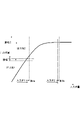
 図1に示されるように、第1実施形態に係る検査装置1は、計測対象物であって被検査デバイス(DUT:Device Under Test)である半導体デバイスDにおける異常発生箇所を特定する等、半導体デバイスDを検査するための装置である。より詳細には、検査装置1は、EOP又はEOFMと称される光プロービング技術により故障位置を特定する。半導体デバイスDとしては、トランジスタ等のPNジャンクションを有する集積回路(IC:Integrated Circuit)、あるいは大規模集積回路(LSI:Large Scale Integration)であるロジックデバイス、メモリデバイス、アナログデバイス、さらに、それらを組み合わせたミックスドシグナルデバイス、または、大電流用/高圧用MOSトランジスタ、バイポーラトランジスタ、IGBT等の電力用半導体デバイス(パワーデバイス)であってもよい。
[First Embodiment]
As shown in FIG. 1, the inspection device 1 according to the first embodiment is a semiconductor such as identifying an abnormality occurrence location in a semiconductor device D which is a measurement target and is a device to be inspected (DUT: Device Under Test). It is a device for inspecting the device D. More specifically, the inspection device 1 identifies the failure position by an optical probing technique called EOP or EOFM. The semiconductor device D includes an integrated circuit (IC: Integrated Circuit) having a PN junction such as a transistor, a logic device, a memory device, an analog device, which is a large-scale integrated circuit (LSI: Large Scale Integration), and a combination thereof. It may be a mixed signal device, or a power semiconductor device (power device) such as a high current / high pressure MOS transistor, a bipolar transistor, or an IGBT.
 検査装置1は、テスタヘッド2と、テストボード3と、ステージ5と、対物レンズ6と、ターレット7と、結像光学系8と、スキャン光学系9と、スキャンユニット11と、光計測部12と、デジタイジングユニット13と、制御装置14と、入出力装置15と、を備えている。ステージ5、対物レンズ6、ターレット7、結像光学系8及びスキャン光学系9は、暗箱4に収容されている。ステージ5は、暗箱4内に収容される各構成を保持する台である。 The inspection device 1 includes a tester head 2, a test board 3, a stage 5, an objective lens 6, a turret 7, an imaging optical system 8, a scan optical system 9, a scan unit 11, and an optical measurement unit 12. A digitizing unit 13, a control device 14, and an input / output device 15 are provided. The stage 5, the objective lens 6, the turret 7, the imaging optical system 8, and the scanning optical system 9 are housed in the dark box 4. The stage 5 is a table that holds each configuration housed in the dark box 4.
 テスタヘッド2は、テストボード3を介して半導体デバイスDを搭載し、半導体デバイスDに所定の動作パルス信号を繰り返し印可する。半導体デバイスDは、当該テスト信号によって駆動する。テスタヘッド2は、例えば、半導体デバイスDを駆動させるための動作パルス信号を発生させるパルスジェネレータと、動作パルス信号を半導体デバイスDに入力するテスタ部と、電源とを有している。テストボード3は、半導体デバイスDを搭載する半導体基板である。テストボード3は、半導体デバイスDの動作に必要な周辺チップ、回路、及び端子等を有している。 The tester head 2 mounts the semiconductor device D via the test board 3 and repeatedly applies a predetermined operation pulse signal to the semiconductor device D. The semiconductor device D is driven by the test signal. The tester head 2 has, for example, a pulse generator that generates an operation pulse signal for driving the semiconductor device D, a tester unit that inputs the operation pulse signal to the semiconductor device D, and a power supply. The test board 3 is a semiconductor substrate on which the semiconductor device D is mounted. The test board 3 has peripheral chips, circuits, terminals, and the like necessary for the operation of the semiconductor device D.
 スキャン光学系9は、光ファイバ10を介して、光計測部12の光源121(図2参照)から出射された光を受け、当該光を結像光学系8に導光する。詳細には、光源121からの光は、光カプラ122(図2参照)を通過し、光ファイバ10によってスキャン光学系9に導光される。光ファイバ10のファイバ端は反射光を低減するために例えばAPC型であってもよい。スキャン光学系9は、例えば、ガルバノミラーやMEMS(micro electro mechanical system)ミラー等の光走査素子を含む光スキャナを有している。スキャン光学系9は、光計測部12の光源121から出射された光を半導体デバイスD上の選択領域に照射(走査)する。当該選択領域は、ユーザにより選択されたスポットもしくはエリアである。スキャンユニット11は、制御装置14による制御に基づき、選択領域のスポットに光が照射されるようにスキャン光学系9を制御する。 The scan optical system 9 receives the light emitted from the light source 121 (see FIG. 2) of the optical measurement unit 12 via the optical fiber 10 and guides the light to the imaging optical system 8. Specifically, the light from the light source 121 passes through the optical coupler 122 (see FIG. 2) and is guided to the scan optical system 9 by the optical fiber 10. The fiber end of the optical fiber 10 may be, for example, an APC type in order to reduce reflected light. The scan optical system 9 has, for example, an optical scanner including an optical scanning element such as a galvano mirror or a MEMS (microelectromechanical system) mirror. The scanning optical system 9 irradiates (scans) the selected region on the semiconductor device D with the light emitted from the light source 121 of the optical measuring unit 12. The selected area is a spot or area selected by the user. The scan unit 11 controls the scan optical system 9 so that the spot in the selected region is irradiated with light based on the control by the control device 14.
 結像光学系8は、スキャン光学系9を介して、光計測部12の光源121から出射された光を受け、当該光を対物レンズ6に導光する。対物レンズ6は、光計測部12の光源121からの光を半導体デバイスDに集光するレンズである。対物レンズ6は、ターレット7により、低倍率対物レンズ(例えば5倍)と高倍率対物レンズ(例えば50倍)とを切替可能に構成されている。半導体デバイスDからの反射光(戻り光)は、対物レンズ6、結像光学系8、スキャン光学系9、及び光ファイバ10を介して光計測部12に入力される。このように、対物レンズ6、結像光学系8、及びスキャン光学系9は、光計測部12の光源121からの光を半導体デバイスDに照射すると共に、半導体デバイスDからの反射光(戻り光)を光計測部12の光増幅器123(図2参照)に導光する光学系である。 The imaging optical system 8 receives the light emitted from the light source 121 of the optical measurement unit 12 via the scan optical system 9 and guides the light to the objective lens 6. The objective lens 6 is a lens that collects the light from the light source 121 of the light measuring unit 12 onto the semiconductor device D. The objective lens 6 is configured to be switchable between a low magnification objective lens (for example, 5 times) and a high magnification objective lens (for example, 50 times) by a turret 7. The reflected light (return light) from the semiconductor device D is input to the optical measurement unit 12 via the objective lens 6, the imaging optical system 8, the scan optical system 9, and the optical fiber 10. As described above, the objective lens 6, the imaging optical system 8, and the scan optical system 9 irradiate the semiconductor device D with the light from the light source 121 of the optical measurement unit 12, and the reflected light (return light) from the semiconductor device D. ) Is an optical system that guides the light to the optical amplifier 123 (see FIG. 2) of the optical measurement unit 12.
 図2に示されるように、光計測部12は、光源121と、光カプラ122と、光増幅器123と、光検出器124と、高周波アンプ125と、を備えている。 As shown in FIG. 2, the optical measurement unit 12 includes a light source 121, an optical coupler 122, an optical amplifier 123, a photodetector 124, and a high frequency amplifier 125.
 光源121は、電源(図示せず)によって動作させられ、半導体デバイスDに照射される光を発生し出力する。当該光は、コヒーレントな光であってもよいしインコヒーレントな光であってもよい。光源121としては、例えば、SLD(Super Luminescent Diode)やASE(Amplified Spontaneous Emission)光源、LED(Light Emitting Diode)等を用いることができる。光源121から出力された光は、光カプラ122及び光ファイバ10を介してスキャン光学系9に導かれる。光カプラ122は、PBS(Polarizing Beam Splitter)型の光カプラもしくはサーキュレータ型の光カプラである。光カプラ122がPBS型の光カプラである場合、スキャン光学系9の内部にλ/4波長板を設けてもよい。また、光カプラ122がサーキュレータ型の光カプラである場合、スキャン光学系9の内部にλ/2波長板を設けてもよい。また、光カプラ122には光スプリッタを代わりに用いてもよい。また、スキャン光学系9の内部には、上述した波長板の代わりにファラデーローテータを設けてもよい。 The light source 121 is operated by a power source (not shown) to generate and output light emitted to the semiconductor device D. The light may be coherent light or incoherent light. As the light source 121, for example, an SLD (Super Luminescent Diode), an ASE (Amplified Spontaneous Emission) light source, an LED (Light Emitting Diode), or the like can be used. The light output from the light source 121 is guided to the scan optical system 9 via the optical coupler 122 and the optical fiber 10. The optical coupler 122 is a PBS (Polarizing Beam Splitter) type optical coupler or a circulator type optical coupler. When the optical coupler 122 is a PBS type optical coupler, a λ / 4 wave plate may be provided inside the scan optical system 9. When the optical coupler 122 is a circulator type optical coupler, a λ / 2 wave plate may be provided inside the scan optical system 9. Further, an optical splitter may be used instead for the optical coupler 122. Further, a Faraday rotator may be provided inside the scan optical system 9 instead of the above-mentioned wave plate.
 光増幅器123は、半導体デバイスDからの反射光(戻り光)を光ファイバ10及び光カプラ122を介して受け、当該反射光(入力された光)の強度を増幅して、増幅光を出力する。光増幅器123は、例えば半導体増幅器、光ファイバアンプ(光ファイバ光増幅器)、SOA(Solid Optical Amplifier)、テーパアンプ(テーパー型増幅器)、ブースタ光増幅器等である。また光増幅器123は、結晶やガス、液体等をレーザ媒質とした増幅器であってもよい。光増幅器123が出力した出力光は、光ファイバ10を介して光検出器124に入力される。 The optical amplifier 123 receives the reflected light (return light) from the semiconductor device D via the optical fiber 10 and the optical coupler 122, amplifies the intensity of the reflected light (input light), and outputs the amplified light. .. The optical amplifier 123 is, for example, a semiconductor amplifier, an optical fiber amplifier (optical fiber optical amplifier), an SOA (Solid Optical Amplifier), a taper amplifier (taper type amplifier), a booster optical amplifier, or the like. Further, the optical amplifier 123 may be an amplifier using a crystal, gas, liquid or the like as a laser medium. The output light output by the optical amplifier 123 is input to the photodetector 124 via the optical fiber 10.
 図3は、光増幅器123の入出力特性を示す図である。図3において横軸は光増幅器123への入力光量を、縦軸は光増幅器123からの出力光量を示している。光増幅器123のゲインは、素子(光増幅器)の特性に応じて、波長毎に特定の値が定まっている。そして、光増幅器123から出力可能な光の強度の上限も定まっている。そのため、光増幅器123は、入力される入力光の強度がある値よりも大きくなると光増幅が抑制され、定められたゲインに応じて光を増幅することができなくなる。この場合、光増幅器123の入力光の強度が大きくなっても増幅光の強度は一定となり、光増幅器123の光増幅特性が非線形となる。このように光増幅器123の光増幅特性が非線形となっている状態が、光増幅器123がゲイン飽和となっている状態である。光増幅器123がある波長においてゲイン飽和となっているとは、すなわち、当該ある波長において光の増幅に寄与することが可能な電荷が全て使い切られ、光増幅が抑制されている状態をいう。 FIG. 3 is a diagram showing the input / output characteristics of the optical amplifier 123. In FIG. 3, the horizontal axis shows the amount of input light to the optical amplifier 123, and the vertical axis shows the amount of output light from the optical amplifier 123. The gain of the optical amplifier 123 has a specific value determined for each wavelength according to the characteristics of the element (optical amplifier). Further, the upper limit of the intensity of light that can be output from the optical amplifier 123 is also determined. Therefore, when the intensity of the input input light becomes higher than a certain value, the optical amplifier 123 suppresses the optical amplification and cannot amplify the light according to the predetermined gain. In this case, even if the intensity of the input light of the optical amplifier 123 increases, the intensity of the amplified light becomes constant, and the optical amplification characteristic of the optical amplifier 123 becomes non-linear. The state in which the optical amplification characteristic of the optical amplifier 123 is non-linear is the state in which the gain of the optical amplifier 123 is saturated. The gain saturation of the optical amplifier 123 at a certain wavelength means that all the charges that can contribute to the amplification of light at the certain wavelength are used up and the optical amplification is suppressed.
 図3における入力光1は、光増幅器123が飽和しない強度の光である。図3における入力光2は、光増幅器123が飽和する強度の光である。入力光1が光増幅器123に入力された場合には、光増幅器123の光増幅特性が線形となり、入力光1が線形に増幅される。この場合には、図3に示されるように、入力光1に含まれる微小信号(図3において「振幅」の範囲が示された部分)についても線形に増幅される。この場合の出力光にはASE光(自然放出光)が含まれるためノイズが少し増加する。一方で、入力光2が光増幅器123に入力された場合には、光増幅器123がゲイン飽和となるため、光増幅器123の光増幅特性が非線形となり、入力光2が光増幅器123の出力限界で出力される。この場合には、図3に示されるように、入力光2に含まれる微小信号(微小な揺らぎ)は圧縮されて消えてしまう。 The input light 1 in FIG. 3 is light having an intensity that does not saturate the optical amplifier 123. The input light 2 in FIG. 3 is light having an intensity at which the optical amplifier 123 is saturated. When the input light 1 is input to the optical amplifier 123, the optical amplification characteristic of the optical amplifier 123 becomes linear, and the input light 1 is linearly amplified. In this case, as shown in FIG. 3, the minute signal included in the input light 1 (the portion where the range of "amplitude" is shown in FIG. 3) is also linearly amplified. Since the output light in this case includes ASE light (spontaneous emission light), noise increases a little. On the other hand, when the input light 2 is input to the optical amplifier 123, the optical amplifier 123 becomes gain saturated, so that the optical amplification characteristics of the optical amplifier 123 become non-linear, and the input light 2 reaches the output limit of the optical amplifier 123. It is output. In this case, as shown in FIG. 3, the minute signal (small fluctuation) contained in the input light 2 is compressed and disappears.
 光増幅器の増幅率は、励起電子密度及び光増幅器の長さに依存する。基底状態の電子は光を吸収してしまうので、上述した励起電子密度とは、詳細には、励起状態の電子の密度から基底状態の電子の密度を差し引いたものである。光増幅器は、その長さが長いほど、励起状態の電子と光子とが衝突する回数が多くなり、増幅率が大きくなる。 The amplification factor of the optical amplifier depends on the excited electron density and the length of the optical amplifier. Since the electrons in the ground state absorb light, the excited electron density described above is specifically the density of the electrons in the excited state minus the density of the electrons in the ground state. The longer the length of the optical amplifier, the more times the excited electrons and photons collide with each other, and the larger the amplification factor.
 光増幅器が飽和するとは、励起状態の電子が増幅に使用された結果、光増幅器の出口付近において励起状態の電子の密度が基底状態の電子の密度以下になることにあたる。増幅される光の最大出力は、励起電子密度に依存し、光ファイバアンプであれば励起光の強さ、SOAであれば供給される電流(励起電流)の強さに依存する。光増幅器では、このような励起光又は励起電流を大きくすることによって励起電子の密度を大きくし増幅率を上げることができる。 Saturation of the optical amplifier means that as a result of the electrons in the excited state being used for amplification, the density of the electrons in the excited state becomes lower than the density of the electrons in the ground state near the outlet of the optical amplifier. The maximum output of amplified light depends on the excited electronic density, the intensity of the excited light in the case of an optical fiber amplifier, and the intensity of the supplied current (excitation current) in the case of SOA. In an optical amplifier, the density of excited electrons can be increased and the amplification factor can be increased by increasing the excitation light or the excitation current.
 ここで、光増幅器に対する励起光又は励起電流を大きくした場合には、励起電子の密度と同時に最大出力も増加する。すなわち、励起光等を変化させることによって励起電子の密度を変化させ増幅率を変化させる場合においては、同時に最大出力も変化してしまう。このため、励起光等を変化させることのみによっては、光の飽和/非飽和の状態を適切に切り替えることができない。そこで、出力光を飽和させないために、入力光に対して適正なゲインを持つ増幅素子、すなわち、適正な増幅長さを持つ増幅素子を用いてもよい。なお、入力光を減衰させることによっても、出力光を飽和させない構成とすることができるが、S/Nを悪化させることから、上述したように増幅素子の増幅長さを適切に設計してもよい。 Here, when the excitation light or the excitation current for the optical amplifier is increased, the maximum output increases at the same time as the density of excited electrons. That is, when the density of excited electrons is changed and the amplification factor is changed by changing the excitation light or the like, the maximum output also changes at the same time. Therefore, the saturated / unsaturated state of the light cannot be appropriately switched only by changing the excitation light or the like. Therefore, in order not to saturate the output light, an amplification element having an appropriate gain with respect to the input light, that is, an amplification element having an appropriate amplification length may be used. It should be noted that the output light can be configured not to be saturated by attenuating the input light, but since the S / N is deteriorated, even if the amplification length of the amplification element is appropriately designed as described above. good.
 上述したように、飽和しないように入力光が増幅された場合には、増幅後の出力光には微小なノイズが重畳する。これはノイズフロアと呼ばれ、増幅方法にもよるが例えば5~10dB程度となる。光増幅器123のゲインは、少なくともこれを上回るゲインとされる。 As described above, when the input light is amplified so as not to be saturated, minute noise is superimposed on the amplified output light. This is called a noise floor, and although it depends on the amplification method, it is, for example, about 5 to 10 dB. The gain of the optical amplifier 123 is at least higher than this.
 光増幅器123は、入力された反射光を飽和しないように増幅する。すなわち、光増幅器123は、光増幅器123にて飽和しない範囲且つ光検出器を飽和しない範囲で反射光を増幅する。光増幅器123は、入力された反射光の光量に対する出力する光の光量の変化が線形になるように、入力された光を増幅する。例えば、光増幅器123は、出力する光の光量が、出力可能な最大光量の半分より大きくなるように、入力された光を増幅してもよい。また、例えば、光増幅器123は、出力する光に含まれるショットノイズが光検出器124のサーマルノイズを上回るように、入力された光を増幅してもよい。そして、光増幅器123は、上述したように入力された光を飽和しないように増幅する条件を満たす長さの増幅素子を有する。 The optical amplifier 123 amplifies the input reflected light so as not to saturate it. That is, the optical amplifier 123 amplifies the reflected light in a range in which the optical amplifier 123 does not saturate and the photodetector does not saturate. The optical amplifier 123 amplifies the input light so that the change in the amount of output light with respect to the amount of input reflected light is linear. For example, the optical amplifier 123 may amplify the input light so that the amount of output light is larger than half of the maximum amount of light that can be output. Further, for example, the optical amplifier 123 may amplify the input light so that the shot noise contained in the output light exceeds the thermal noise of the photodetector 124. The optical amplifier 123 has an amplification element having a length satisfying the condition of amplifying the input light so as not to saturate it as described above.
 光検出器124は、光増幅器123から出力された光を検出する光センサである。光検出器124は、高速の光信号を検出する光センサであり、例えば8GHz以上の帯域の光を検出可能に構成された光センサである。光検出器124は、例えばPINフォトダイオードである。高速の光信号を検出可能な光センサ(例えばPINフォトダイオード)を用いる場合、シングルモードファイバでの入力となるため、入射用の光ファイバ10及び光カプラ122等は全てシングルモードファイバの組み合わせで構成されてもよいが、ハーフミラーや偏光ビームスプリッタ、コリメータを組み合わせた光学系で構成されてもよい。なお、光検出器124は、例えば8GHz以上の広帯域の信号を検出可能に構成されたアバランシェフォトダイオード、光電子増倍管、又はエリアイメージセンサ等であってもよい。光検出器124は、検出信号(電気信号)を出力する。光検出器124が出力した検出信号は、高周波ケーブル16によって高周波アンプ125に入力される。高周波アンプ125は、光検出器124から入力された検出信号を増幅し、増幅信号として出力する。 The photodetector 124 is an optical sensor that detects the light output from the optical amplifier 123. The photodetector 124 is an optical sensor that detects a high-speed optical signal, and is, for example, an optical sensor configured to be able to detect light in a band of 8 GHz or higher. The photodetector 124 is, for example, a PIN photodiode. When an optical sensor (for example, a PIN photodiode) capable of detecting a high-speed optical signal is used, the input is a single-mode fiber. Therefore, the optical fiber 10 for incident and the optical coupler 122 are all composed of a combination of single-mode fibers. However, it may be configured by an optical system in which a half mirror, a polarization beam splitter, and a collimator are combined. The photodetector 124 may be, for example, an avalanche photodiode, a photomultiplier tube, an area image sensor, or the like configured to be capable of detecting a wide band signal of 8 GHz or more. The photodetector 124 outputs a detection signal (electrical signal). The detection signal output by the photodetector 124 is input to the high frequency amplifier 125 by the high frequency cable 16. The high frequency amplifier 125 amplifies the detection signal input from the photodetector 124 and outputs it as an amplified signal.
 図1に戻り、デジタイジングユニット13は、高周波アンプ125から入力された増幅信号を波形化して出力する。デジタイジングユニット13は、例えばデジタイザ、オシロスコープ、FPGA等により構成されている。デジタイジングユニット13が出力した波形化信号は、制御装置14に入力される。 Returning to FIG. 1, the digitizing unit 13 waveforms and outputs the amplified signal input from the high frequency amplifier 125. The digitizing unit 13 is composed of, for example, a digitizer, an oscilloscope, an FPGA, or the like. The waveformized signal output by the digitizing unit 13 is input to the control device 14.
 制御装置14は、スキャンユニット11及びデジタイジングユニット13を制御する装置である。制御装置14は、デジタイジングユニット13から取得した波形化信号に基づき波形(解析画像)を生成し、該解析画像を入出力装置15に入力する。入出力装置15は、ユーザから計測条件等が入力されるキーボードやマウス等の入力装置と、ユーザに計測結果等を示すためのモニタ等の表示装置とを有している。入出力装置15は、制御装置14から入力された解析画像を表示する。当該解析画像から、ジッダの計測及びスイッチング画像(波形)の確認等を行い、故障個所の特定等を行うことができる。 The control device 14 is a device that controls the scan unit 11 and the digitizing unit 13. The control device 14 generates a waveform (analyzed image) based on the waveformized signal acquired from the digitizing unit 13, and inputs the analyzed image to the input / output device 15. The input / output device 15 has an input device such as a keyboard and a mouse into which measurement conditions and the like are input from the user, and a display device such as a monitor for showing the measurement result and the like to the user. The input / output device 15 displays the analysis image input from the control device 14. From the analysis image, it is possible to measure the Jeddah, check the switching image (waveform), and identify the faulty part.
 次に、本実施形態に係る検査装置1の作用効果について説明する。 Next, the operation and effect of the inspection device 1 according to the present embodiment will be described.
 最初に、比較例に係る検査装置の構成及びその構成における課題について説明する。LSI等の半導体デバイス上の能動デバイス、例えばトランジスタの光の反射率は10%以下程度であり大きくない。このような半導体デバイスに強い光を当てると、トランジスタ等のデバイスが入射光により破壊されてしまうおそれがある。このため、半導体デバイスに照射される光の光量は、半導体デバイスが破壊されない程度に小さくされる。例えば、開口数1以上を実現する固浸レンズを用いる場合においては、照射される光の光量は数mWが上限とされ、その場合の反射光(戻り光)の上限は0.1mW程度となる。そして、理想的な計測のためには、光のショットノイズを計測器(詳細には光検出器等)のサーマルノイズよりも大きくしてもよい。比較例に係る検査装置(一般的な検査装置)では、上述したように戻り光の光量が小さくなる構成においてショットノイズをサーマルノイズよりも大きくするために、戻り光を増幅する増倍層を有する光検出器(例えばAPD等の光検出器)が採用されている。このような光検出器が用いられることにより、ショットノイズをサーマルノイズよりも大きくして、精度の高い検査を行うことができる。 First, the configuration of the inspection device according to the comparative example and the problems in the configuration will be explained. The light reflectance of an active device on a semiconductor device such as an LSI, for example, a transistor, is about 10% or less, which is not large. When a strong light is applied to such a semiconductor device, the device such as a transistor may be destroyed by the incident light. Therefore, the amount of light emitted to the semiconductor device is reduced to such an extent that the semiconductor device is not destroyed. For example, when a solid immersion lens having a numerical aperture of 1 or more is used, the upper limit of the amount of irradiated light is several mW, and the upper limit of the reflected light (return light) in that case is about 0.1 mW. .. Then, for ideal measurement, the shot noise of light may be larger than the thermal noise of a measuring instrument (specifically, a photodetector or the like). The inspection device (general inspection device) according to the comparative example has a multiplier layer that amplifies the return light in order to make the shot noise larger than the thermal noise in a configuration in which the amount of return light is small as described above. A photodetector (for example, a photodetector such as APD) is adopted. By using such a photodetector, shot noise can be made larger than thermal noise, and highly accurate inspection can be performed.
 ここで、近年、半導体デバイスの性能向上に伴って、より高い周波数帯域を含む広帯域の現象を検出することができる検査装置が求められている。具体的には、例えば、微小なジッダ(例えば10ps程度のジッダ)を正確に検出することができる検査装置が求められている。この点、上述した比較例に係る光検出器を有する検査装置では、光検出器の容量が比較的大きくなるため、高速な信号の検出(高い周波数帯域の現象の検出)を行うことができない。具体的には、比較例に係る光検出器(例えばAPD)は、P層とN層との間に増倍層を有し、当該増倍層に強い電界がかけられる。強い電界がかけられる増倍層を有する光検出器においては、その容量が比較的大きくなってしまい、高速な信号の検出(高い周波数帯域の現象の検出)を行うことができない。 Here, in recent years, with the improvement of the performance of semiconductor devices, there is a demand for an inspection device capable of detecting a wide band phenomenon including a higher frequency band. Specifically, for example, there is a demand for an inspection device capable of accurately detecting a minute Jeddah (for example, a Jeddah of about 10 ps). In this respect, in the inspection device having the photodetector according to the above-mentioned comparative example, the capacity of the photodetector is relatively large, so that high-speed signal detection (detection of a phenomenon in a high frequency band) cannot be performed. Specifically, the photodetector (for example, APD) according to the comparative example has a multiplying layer between the P layer and the N layer, and a strong electric field is applied to the multiplying layer. In a photodetector having a multiplier layer to which a strong electric field is applied, its capacitance becomes relatively large, and high-speed signal detection (detection of a phenomenon in a high frequency band) cannot be performed.
 このような課題を解決する構成として、本実施形態に係る検査装置1は、光を発生する光源121と、入力された光を増幅して出力する光増幅器123と、光源121からの光を半導体デバイスDに照射し、該半導体デバイスDからの光を光増幅器123に導光する光学系(対物レンズ6、結像光学系8、及びスキャン光学系9)と、光増幅器123から出力された光を検出する光検出器124と、を備え、光増幅器123は、入力された光を飽和しないように増幅する。 As a configuration for solving such a problem, the inspection device 1 according to the present embodiment has a light source 121 that generates light, an optical amplifier 123 that amplifies and outputs the input light, and a semiconductor that outputs light from the light source 121. The optical system (objective lens 6, imaging optical system 8, and scan optical system 9) that irradiates the device D and guides the light from the semiconductor device D to the optical amplifier 123, and the light output from the optical amplifier 123. The optical amplifier 123 includes an optical detector 124 for detecting the light, and the optical amplifier 123 amplifies the input light so as not to saturate it.
 本実施形態に係る検査装置1では、光検出器124とは別に光増幅器123が設けられており、該光増幅器123において増幅された光が光検出器124において検出されるため、検出精度を担保するための信号の増幅については光増幅器123によって行い、増幅後の光の検出を光検出器124によって行うことが可能になる。このような構成においては、光検出器124として、増倍層を有さず比較的容量が小さい光検出器(例えばPINフォトダイオード)を用いることができるため、高い周波数帯域(例えば10GHzを超える、20GHz程度の帯域)の現象を検出することができる。また、本実施形態に係る検査装置1では、光増幅器123によって、飽和しない範囲で光が増幅されている。飽和する場合には、入力光に含まれる微小信号が増幅後において消えてしまい、微小信号が適切に検出されないおそれがある。この点、飽和しない範囲で光が増幅されることにより、微小信号を含んだ出力光に基づき、微小な現象(例えばジッダ等)についても正確に検出することができる。以上のように、本実施形態に係る検査装置1によれば、高い周波数帯域を含む広帯域の現象を正確に検出することができる。 In the inspection device 1 according to the present embodiment, an optical amplifier 123 is provided separately from the photodetector 124, and the light amplified by the photodetector 123 is detected by the photodetector 124, so that the detection accuracy is guaranteed. The amplification of the signal for this purpose is performed by the optical amplifier 123, and the detection of the amplified light can be performed by the photodetector 124. In such a configuration, as the photodetector 124, a photodetector having a relatively small capacity (for example, a PIN photodiode) without a multiplying layer can be used, so that a high frequency band (for example, exceeding 10 GHz) can be used. It is possible to detect a phenomenon (band of about 20 GHz). Further, in the inspection device 1 according to the present embodiment, the light is amplified in a non-saturated range by the optical amplifier 123. When saturated, the minute signal contained in the input light disappears after amplification, and the minute signal may not be detected properly. In this respect, by amplifying the light in a non-saturating range, it is possible to accurately detect even a minute phenomenon (for example, Jeddah) based on the output light including a minute signal. As described above, according to the inspection device 1 according to the present embodiment, it is possible to accurately detect the phenomenon of a wide band including a high frequency band.
 光増幅器123は、入力された光の光量に対する出力する光の光量の変化が線形になるように、入力された光を増幅してもよい。このように、入力光と出力光とが線形の関係にあることによって、半導体デバイスDからの戻り光に係る現象を正確に検出することができる。 The optical amplifier 123 may amplify the input light so that the change in the amount of output light with respect to the amount of input light is linear. As described above, the linear relationship between the input light and the output light makes it possible to accurately detect the phenomenon related to the return light from the semiconductor device D.
 光増幅器123は、出力する光の光量が、出力可能な最大光量の半分の光量より大きくなるように、入力された光を増幅してもよい。これにより、飽和しないようにしながら、十分に増幅率を大きくすることができ、現象の検出精度を担保することができる。 The optical amplifier 123 may amplify the input light so that the amount of light to be output is larger than the amount of light that is half of the maximum amount of light that can be output. As a result, the amplification factor can be sufficiently increased while preventing saturation, and the detection accuracy of the phenomenon can be ensured.
 光増幅器123は、出力する光に含まれるショットノイズが光検出器124のサーマルノイズを上回るように、入力された光を増幅してもよい。このように、光検出器124に係るノイズよりも光に含まれるノイズが大きくなるように光が増幅されることにより、光に含まれるノイズ(ショットノイズや相対強度ノイズ)が支配的になり、光検出器124に係るノイズ(サーマルノイズ)の影響によって検出精度が悪化することを防止できる。 The optical amplifier 123 may amplify the input light so that the shot noise contained in the output light exceeds the thermal noise of the photodetector 124. In this way, by amplifying the light so that the noise contained in the light becomes larger than the noise related to the photodetector 124, the noise contained in the light (shot noise and relative intensity noise) becomes dominant. It is possible to prevent the detection accuracy from deteriorating due to the influence of noise (thermal noise) related to the photodetector 124.
 光増幅器123は、入力された光を飽和しないように増幅する条件を満たす長さの増幅素子を有していてもよい。これにより、飽和しないように設定された条件で、入力された光を適切に増幅することができる。 The optical amplifier 123 may have an amplification element having a length satisfying the condition of amplifying the input light so as not to saturate it. As a result, the input light can be appropriately amplified under the conditions set so as not to be saturated.
 光増幅器123は、半導体増幅器、光ファイバ光増幅器、又はテーパー型増幅器であってもよい。これにより、上述した飽和しない範囲での光の増幅を適切に行うことができる。 The optical amplifier 123 may be a semiconductor amplifier, an optical fiber optical amplifier, or a tapered amplifier. This makes it possible to appropriately amplify the light in the above-mentioned non-saturating range.
 光検出器124は、PINフォトダイオードであってもよい。このように、比較的容量が小さいPINフォトダイオードが光検出器として用いられることにより、高い周波数帯域の現象を検出することができる。 The photodetector 124 may be a PIN photodiode. As described above, by using a PIN photodiode having a relatively small capacity as a photodetector, it is possible to detect a phenomenon in a high frequency band.
 光検出器124は、8GHz以上の帯域の光を検出可能に構成されていてもよい。これにより、高い周波数帯域の現象を検出することができる。 The photodetector 124 may be configured to be capable of detecting light in a band of 8 GHz or higher. This makes it possible to detect a phenomenon in a high frequency band.
 1…検査装置、6…対物レンズ(光学系)、8…結像光学系(光学系)、9…スキャン光学系(光学系)、121…光源、123…光増幅器、124…光検出器。 1 ... Inspection device, 6 ... Objective lens (optical system), 8 ... Imaging optical system (optical system), 9 ... Scan optical system (optical system), 121 ... Light source, 123 ... Optical amplifier, 124 ... Optical detector.

Claims (8)

  1.  光を発生する光源と、
     入力された光を増幅して出力する光増幅器と、
     前記光源からの光を半導体デバイスに照射し、該半導体デバイスからの光を前記光増幅器に導光する光学系と、
     前記光増幅器から出力された光を検出する光検出器と、を備え、
     前記光増幅器は、前記入力された光を飽和しないように増幅する、検査装置。
    A light source that generates light and
    An optical amplifier that amplifies and outputs the input light, and
    An optical system that irradiates a semiconductor device with light from the light source and guides the light from the semiconductor device to the optical amplifier.
    A photodetector that detects the light output from the optical amplifier is provided.
    The optical amplifier is an inspection device that amplifies the input light so as not to saturate it.
  2.  前記光増幅器は、前記入力された光の光量に対する出力する光の光量の変化が線形になるように、前記入力された光を増幅する、請求項1記載の検査装置。 The inspection device according to claim 1, wherein the optical amplifier amplifies the input light so that the change in the light amount of the output light with respect to the light amount of the input light becomes linear.
  3.  前記光増幅器は、出力する光の光量が、出力可能な最大光量の半分の光量より大きくなるように、前記入力された光を増幅する、請求項1又は2記載の検査装置。 The inspection device according to claim 1 or 2, wherein the optical amplifier amplifies the input light so that the amount of light to be output is larger than the amount of light that is half of the maximum amount of light that can be output.
  4.  前記光増幅器は、出力する光に含まれるショットノイズが前記光検出器のサーマルノイズを上回るように、前記入力された光を増幅する、請求項1~3のいずれか一項記載の検査装置。 The inspection device according to any one of claims 1 to 3, wherein the optical amplifier amplifies the input light so that the shot noise contained in the output light exceeds the thermal noise of the photodetector.
  5.  前記光増幅器は、前記入力された光を飽和しないように増幅する条件を満たす長さの増幅素子を有する、請求項1~4のいずれか一項記載の検査装置。 The inspection device according to any one of claims 1 to 4, wherein the optical amplifier has an amplification element having a length satisfying the condition of amplifying the input light so as not to saturate it.
  6.  前記光増幅器は、半導体増幅器、光ファイバ光増幅器、又はテーパー型増幅器である、請求項1~5のいずれか一項記載の検査装置。 The inspection device according to any one of claims 1 to 5, wherein the optical amplifier is a semiconductor amplifier, an optical fiber optical amplifier, or a tapered amplifier.
  7.  前記光検出器は、PINフォトダイオードである、請求項1~6のいずれか一項記載の検査装置。 The inspection device according to any one of claims 1 to 6, wherein the photodetector is a PIN photodiode.
  8.  前記光検出器は、8GHz以上の帯域の光を検出可能に構成されている、請求項1~7のいずれか一項記載の検査装置。 The inspection device according to any one of claims 1 to 7, wherein the photodetector is configured to be capable of detecting light in a band of 8 GHz or higher.
PCT/JP2021/024153 2020-09-23 2021-06-25 Inspection device WO2022064798A1 (en)

Priority Applications (5)

Application Number Priority Date Filing Date Title
KR1020227043070A KR20230070410A (en) 2020-09-23 2021-06-25 inspection device
US18/020,273 US20240012047A1 (en) 2020-09-23 2021-06-25 Inspection device
EP21871930.0A EP4213189A1 (en) 2020-09-23 2021-06-25 Inspection device
CN202180064713.2A CN116195042A (en) 2020-09-23 2021-06-25 Inspection apparatus
JP2022551149A JPWO2022064798A1 (en) 2020-09-23 2021-06-25

Applications Claiming Priority (2)

Application Number Priority Date Filing Date Title
JP2020158395 2020-09-23
JP2020-158395 2020-09-23

Publications (1)

Publication Number Publication Date
WO2022064798A1 true WO2022064798A1 (en) 2022-03-31

Family

ID=80845240

Family Applications (1)

Application Number Title Priority Date Filing Date
PCT/JP2021/024153 WO2022064798A1 (en) 2020-09-23 2021-06-25 Inspection device

Country Status (7)

Country Link
US (1) US20240012047A1 (en)
EP (1) EP4213189A1 (en)
JP (1) JPWO2022064798A1 (en)
KR (1) KR20230070410A (en)
CN (1) CN116195042A (en)
TW (1) TW202212847A (en)
WO (1) WO2022064798A1 (en)

Cited By (1)

* Cited by examiner, † Cited by third party
Publication number Priority date Publication date Assignee Title
WO2024018774A1 (en) * 2022-07-22 2024-01-25 国立研究開発法人産業技術総合研究所 High-frequency imaging device

Citations (10)

* Cited by examiner, † Cited by third party
Publication number Priority date Publication date Assignee Title
JPS6088441A (en) * 1983-09-23 1985-05-18 シーメンス、アクチエンゲゼルシヤフト Method of measuring lapse of signal at measuring point
JPH06109584A (en) * 1992-01-09 1994-04-19 Hikari Keisoku Gijutsu Kaihatsu Kk Optical fiber measuring apparatus
JPH06160035A (en) * 1992-11-16 1994-06-07 Matsushita Electric Ind Co Ltd Substrate inspection device
JP2000244417A (en) * 1999-02-22 2000-09-08 Nec Eng Ltd Optical pre-amplifier
JP2007064975A (en) 2005-08-26 2007-03-15 Credence Systems Corp Modulation map display system and method
WO2011004536A1 (en) * 2009-07-10 2011-01-13 日本電気株式会社 Electromagnetic field measuring device, electromagnetic field measuring method used for the measuring device, and non-transitory computer-readable medium in which electromagnetic field measurement control program is stored
JP2011022148A (en) * 2002-02-26 2011-02-03 Kla-Tencor Corp Apparatus for optically inspecting sample for discovering anomalies
JP2012038805A (en) * 2010-08-04 2012-02-23 Precise Gauges Co Ltd Detector for detecting electric field distribution or carrier distribution based on intensity of higher order harmonic
JP2015105851A (en) * 2013-11-29 2015-06-08 浜松ホトニクス株式会社 Semiconductor device measuring apparatus and semiconductor device measuring method
US20170019170A1 (en) * 2014-03-07 2017-01-19 Keysight Technologies, Inc. Dual-Directional Electro-Optic Probe

Patent Citations (10)

* Cited by examiner, † Cited by third party
Publication number Priority date Publication date Assignee Title
JPS6088441A (en) * 1983-09-23 1985-05-18 シーメンス、アクチエンゲゼルシヤフト Method of measuring lapse of signal at measuring point
JPH06109584A (en) * 1992-01-09 1994-04-19 Hikari Keisoku Gijutsu Kaihatsu Kk Optical fiber measuring apparatus
JPH06160035A (en) * 1992-11-16 1994-06-07 Matsushita Electric Ind Co Ltd Substrate inspection device
JP2000244417A (en) * 1999-02-22 2000-09-08 Nec Eng Ltd Optical pre-amplifier
JP2011022148A (en) * 2002-02-26 2011-02-03 Kla-Tencor Corp Apparatus for optically inspecting sample for discovering anomalies
JP2007064975A (en) 2005-08-26 2007-03-15 Credence Systems Corp Modulation map display system and method
WO2011004536A1 (en) * 2009-07-10 2011-01-13 日本電気株式会社 Electromagnetic field measuring device, electromagnetic field measuring method used for the measuring device, and non-transitory computer-readable medium in which electromagnetic field measurement control program is stored
JP2012038805A (en) * 2010-08-04 2012-02-23 Precise Gauges Co Ltd Detector for detecting electric field distribution or carrier distribution based on intensity of higher order harmonic
JP2015105851A (en) * 2013-11-29 2015-06-08 浜松ホトニクス株式会社 Semiconductor device measuring apparatus and semiconductor device measuring method
US20170019170A1 (en) * 2014-03-07 2017-01-19 Keysight Technologies, Inc. Dual-Directional Electro-Optic Probe

Cited By (1)

* Cited by examiner, † Cited by third party
Publication number Priority date Publication date Assignee Title
WO2024018774A1 (en) * 2022-07-22 2024-01-25 国立研究開発法人産業技術総合研究所 High-frequency imaging device

Also Published As

Publication number Publication date
CN116195042A (en) 2023-05-30
US20240012047A1 (en) 2024-01-11
KR20230070410A (en) 2023-05-23
TW202212847A (en) 2022-04-01
JPWO2022064798A1 (en) 2022-03-31
EP4213189A1 (en) 2023-07-19

Similar Documents

Publication Publication Date Title
US10191104B2 (en) Semiconductor device inspection device and semiconductor device inspection method
JP6166032B2 (en) Semiconductor device inspection apparatus and semiconductor device inspection method
KR102403498B1 (en) Light source device and inspection device
US9618576B2 (en) Apparatus for testing a semiconductor device and method of testing a semiconductor device
WO2022064798A1 (en) Inspection device
US11415525B2 (en) Carrier lifespan measurement method and carrier lifespan measurement device
US10139447B2 (en) Image generation apparatus and image generation method
US11573251B2 (en) Semiconductor sample inspection device and inspection method
US20200408730A1 (en) Concentration measurement method and concentration measurement device
WO2019230147A1 (en) Optical difference detector and inspection device
JP2016223899A (en) Light source device and inspection device
JPH04238238A (en) Coherent light source

Legal Events

Date Code Title Description
121 Ep: the epo has been informed by wipo that ep was designated in this application

Ref document number: 21871930

Country of ref document: EP

Kind code of ref document: A1

ENP Entry into the national phase

Ref document number: 2022551149

Country of ref document: JP

Kind code of ref document: A

WWE Wipo information: entry into national phase

Ref document number: 18020273

Country of ref document: US

ENP Entry into the national phase

Ref document number: 2021871930

Country of ref document: EP

Effective date: 20230411

NENP Non-entry into the national phase

Ref country code: DE