WO2022029952A1 - Data recorder and method for using data recorder - Google Patents
Data recorder and method for using data recorder Download PDFInfo
- Publication number
- WO2022029952A1 WO2022029952A1 PCT/JP2020/030134 JP2020030134W WO2022029952A1 WO 2022029952 A1 WO2022029952 A1 WO 2022029952A1 JP 2020030134 W JP2020030134 W JP 2020030134W WO 2022029952 A1 WO2022029952 A1 WO 2022029952A1
- Authority
- WO
- WIPO (PCT)
- Prior art keywords
- data
- volatile memory
- power supply
- control unit
- data recorder
- Prior art date
Links
- 238000000034 method Methods 0.000 title claims description 104
- 230000015654 memory Effects 0.000 claims abstract description 523
- 230000005855 radiation Effects 0.000 claims abstract description 57
- 238000012546 transfer Methods 0.000 claims abstract description 40
- 230000008569 process Effects 0.000 claims description 89
- 238000012545 processing Methods 0.000 claims description 33
- 238000012544 monitoring process Methods 0.000 claims description 30
- 238000012937 correction Methods 0.000 claims description 17
- 230000000694 effects Effects 0.000 abstract description 43
- 230000002411 adverse Effects 0.000 abstract description 32
- 238000004891 communication Methods 0.000 description 38
- 230000005540 biological transmission Effects 0.000 description 30
- 238000010586 diagram Methods 0.000 description 14
- 230000008054 signal transmission Effects 0.000 description 9
- 230000006870 function Effects 0.000 description 7
- 238000012986 modification Methods 0.000 description 7
- 230000004048 modification Effects 0.000 description 7
- 230000008859 change Effects 0.000 description 6
- 239000004065 semiconductor Substances 0.000 description 5
- 230000007423 decrease Effects 0.000 description 3
- LFHISGNCFUNFFM-UHFFFAOYSA-N chloropicrin Chemical compound [O-][N+](=O)C(Cl)(Cl)Cl LFHISGNCFUNFFM-UHFFFAOYSA-N 0.000 description 2
- 238000012790 confirmation Methods 0.000 description 2
- 238000013479 data entry Methods 0.000 description 2
- 238000013461 design Methods 0.000 description 2
- 230000003287 optical effect Effects 0.000 description 2
- 230000005856 abnormality Effects 0.000 description 1
- 238000009825 accumulation Methods 0.000 description 1
- 230000000295 complement effect Effects 0.000 description 1
- 239000002131 composite material Substances 0.000 description 1
- 230000005611 electricity Effects 0.000 description 1
- 238000005516 engineering process Methods 0.000 description 1
- 230000006872 improvement Effects 0.000 description 1
- 239000002245 particle Substances 0.000 description 1
- 239000000941 radioactive substance Substances 0.000 description 1
Images


Classifications
-
- G—PHYSICS
- G06—COMPUTING; CALCULATING OR COUNTING
- G06F—ELECTRIC DIGITAL DATA PROCESSING
- G06F12/00—Accessing, addressing or allocating within memory systems or architectures
- G06F12/02—Addressing or allocation; Relocation
- G06F12/0223—User address space allocation, e.g. contiguous or non contiguous base addressing
- G06F12/023—Free address space management
- G06F12/0238—Memory management in non-volatile memory, e.g. resistive RAM or ferroelectric memory
- G06F12/0246—Memory management in non-volatile memory, e.g. resistive RAM or ferroelectric memory in block erasable memory, e.g. flash memory
-
- G—PHYSICS
- G06—COMPUTING; CALCULATING OR COUNTING
- G06F—ELECTRIC DIGITAL DATA PROCESSING
- G06F11/00—Error detection; Error correction; Monitoring
- G06F11/07—Responding to the occurrence of a fault, e.g. fault tolerance
- G06F11/0703—Error or fault processing not based on redundancy, i.e. by taking additional measures to deal with the error or fault not making use of redundancy in operation, in hardware, or in data representation
- G06F11/0793—Remedial or corrective actions
-
- G—PHYSICS
- G06—COMPUTING; CALCULATING OR COUNTING
- G06F—ELECTRIC DIGITAL DATA PROCESSING
- G06F11/00—Error detection; Error correction; Monitoring
- G06F11/07—Responding to the occurrence of a fault, e.g. fault tolerance
- G06F11/0703—Error or fault processing not based on redundancy, i.e. by taking additional measures to deal with the error or fault not making use of redundancy in operation, in hardware, or in data representation
- G06F11/0706—Error or fault processing not based on redundancy, i.e. by taking additional measures to deal with the error or fault not making use of redundancy in operation, in hardware, or in data representation the processing taking place on a specific hardware platform or in a specific software environment
- G06F11/073—Error or fault processing not based on redundancy, i.e. by taking additional measures to deal with the error or fault not making use of redundancy in operation, in hardware, or in data representation the processing taking place on a specific hardware platform or in a specific software environment in a memory management context, e.g. virtual memory or cache management
-
- G—PHYSICS
- G06—COMPUTING; CALCULATING OR COUNTING
- G06F—ELECTRIC DIGITAL DATA PROCESSING
- G06F2212/00—Indexing scheme relating to accessing, addressing or allocation within memory systems or architectures
- G06F2212/10—Providing a specific technical effect
- G06F2212/1028—Power efficiency
-
- G—PHYSICS
- G06—COMPUTING; CALCULATING OR COUNTING
- G06F—ELECTRIC DIGITAL DATA PROCESSING
- G06F2212/00—Indexing scheme relating to accessing, addressing or allocation within memory systems or architectures
- G06F2212/72—Details relating to flash memory management
- G06F2212/7203—Temporary buffering, e.g. using volatile buffer or dedicated buffer blocks
Definitions
- This disclosure relates to a data recorder and how to use the data recorder.
- Patent Document 1 discloses a configuration in which a data recorder controls the power supply of the non-volatile memory module of the data recorder in order to realize power saving.
- the power supply control disclosed in Patent Document 1 has room for improvement from the viewpoint of countermeasures against adverse effects of radiation.
- the present disclosure is to solve such a problem, and an object of the present invention is to provide a data recorder capable of suppressing adverse effects of radiation, and to provide a method of using a data recorder capable of suppressing adverse effects of radiation. ..
- the data recorder of one aspect of the present disclosure includes an input interface, a storage unit, and a control unit, and the storage unit is a non-volatile memory for storing data and a power supply for the non-volatile memory, and the control unit controls on and off.
- the input interface is provided with a first buffer memory, the input interface receives data input from the outside and records it in the first buffer memory, and the control unit is a first buffer.
- the power supply for the non-volatile memory is switched on at the timing determined based on the amount of data recorded in the memory and the mode of data input from the outside via the input interface, and the input interface is the non-volatile memory.
- the control unit transfers the data recorded in the first buffer memory to the non-volatile memory. After that, it is a data recorder that switches off the power supply for non-volatile memory.
- another aspect of the data recorder of the present disclosure includes an output interface, a storage unit, and a control unit, and the storage unit is a non-volatile memory for storing data and a power supply for the non-volatile memory, and is turned on to the control unit.
- the output interface is provided with a second buffer memory, and the control unit transfers the data to be output stored in the non-volatile memory via the second buffer memory. Part of the period from the start of transfer of the data to be output to the second buffer memory to the end of transfer of the data to be output to the second buffer memory when outputting to the outside.
- This is a data recorder that turns off the power supply for non-volatile memory during the period of.
- the data recorder of still another aspect of the present disclosure includes an input interface, an output interface, a storage unit, and a control unit, and the storage unit is a non-volatile memory for storing data and a power supply for the non-volatile memory.
- the control unit is equipped with a power supply for non-volatile memory that can be turned on and off, the input interface is equipped with a first buffer memory, the output interface is equipped with a second buffer memory, and the input interface receives data input from the outside. The timing is determined based on the amount of data recorded in the first buffer memory and the mode of data input from the outside via the input interface.
- the power supply for the non-volatile memory is switched on, and the input interface transfers the data recorded in the first buffer memory to the non-volatile memory when the power supply for the non-volatile memory is on, and the control unit. Transfers the data recorded in the first buffer memory to the non-volatile memory, then switches off the power supply for the non-volatile memory, and the control unit transfers the data to be output stored in the non-volatile memory to the first. When outputting to the outside via the second buffer memory, between the start of transfer of the data to be output to the second buffer memory and the end of transfer of the data to be output to the second buffer memory.
- a data recorder that turns off the power supply for non-volatile memory during a part of the period.
- the method of using the data recorder in one aspect of the present disclosure is a method of using the data recorder, which is a method of using the data recorder of the present disclosure, in which the data recorder is placed in the radiation environment and the data is stored in the data recorder. How to use a data recorder to replay data recorded or recorded in a data recorder.
- the control unit has a timing determined based on the amount of data recorded in the first buffer memory and the mode of data input from the outside via the input interface. , The power supply for non-volatile memory is switched on, the input interface transfers the data recorded in the first buffer memory to the non-volatile memory when the power supply for non-volatile memory is on, and the control unit After transferring the data recorded in the first buffer memory to the non-volatile memory, the power supply for the non-volatile memory is switched off. This provides a data recorder capable of suppressing the adverse effects of radiation.
- the control unit when the control unit outputs the data to be output stored in the non-volatile memory to the outside via the second buffer memory, the control unit outputs the data to be output.
- the power for the non-volatile memory is turned off during a part of the period from the start of the transfer to the second buffer memory to the end of the transfer of the data to be output to the second buffer memory. Make it a state. This provides a data recorder capable of suppressing the adverse effects of radiation.
- the control unit is based on the amount of data recorded in the first buffer memory and the aspect of data input from the outside via the input interface.
- the power supply for the non-volatile memory is switched on, and the input interface transfers the data recorded in the first buffer memory to the non-volatile memory when the power supply for the non-volatile memory is on.
- the control unit switches off the power supply for the non-volatile memory, and the control unit is the output target stored in the non-volatile memory.
- the data of The power for the non-volatile memory is turned off during a part of the period up to. This provides a data recorder capable of suppressing the adverse effects of radiation.
- the method of using the data recorder in one aspect of the present disclosure is a method of using the data recorder, which is a method of using the data recorder of the present disclosure, in which the data recorder is placed in the radiation environment and the data is stored in the data recorder. How to use a data recorder to replay data recorded or recorded in a data recorder. This provides a method of using a data recorder that can suppress the adverse effects of radiation.
- FIG. It is a block diagram which shows the structure of the data recorder of Embodiment 1.
- FIG. It is a flowchart of the data reception processing of the data recorder of Embodiment 1. It is a flowchart of the storage process of the data recorder of Embodiment 1. It is a flowchart of the reproduction data reading process of the data recorder of Embodiment 1. It is a flowchart of the reproduction processing of the data recorder of Embodiment 1.
- FIG. It is a figure for demonstrating operation of the data recorder of Embodiment 2.
- FIG. It is a figure for demonstrating operation of the data recorder of Embodiment 2.
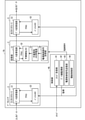
- FIG. 1 is a block diagram showing a configuration of a data recorder 1 which is a data recorder according to the first embodiment.
- the data recorder 1 includes an input interface 2, a storage unit 3, a control unit 4, and an output interface 5.
- the input interface 2 includes a data transmission / reception unit 21 and a buffer memory 22 (first buffer memory).
- the input interface 2 receives data transmitted from the outside of the data recorder 1 and transfers the data to the storage unit 3.
- the input interface 2 temporarily stores the data received from the outside in the buffer memory 22. By temporarily storing the data received from the outside in the buffer memory 22, there is a grace period for turning off the power supply 33 for the non-volatile memory provided in the storage unit 3 as described later.
- the storage unit 3 includes a data transmission / reception unit 31, a non-volatile memory 32, a power supply 33 for the non-volatile memory, and a power supply control signal reception unit 34.
- the data transmission / reception unit 31 receives the data transferred from the input interface 2 and stores it in the non-volatile memory 32. Further, when the data is reproduced, the data is read from the non-volatile memory 32 and the data is transferred to the output interface 5.
- the non-volatile memory 32 is a non-volatile semiconductor memory such as a flash memory, an MRAM, or an EEPROM.
- the power supply 33 for the non-volatile memory is a power supply that supplies power to the non-volatile memory 32, and is switched on and off by the control signal of the power supply transferred from the power supply control signal receiving unit 34.
- the power supply control signal receiving unit 34 receives the power supply control signal transmitted from the control unit 4, and transfers the received power supply control signal to the power supply 33 for the non-volatile memory. In this way, the control unit 4 controls the on / off of the non-volatile memory power supply 33 via the power supply control signal receiving unit 34.
- the control unit 4 includes a command receiving unit 41, a data amount monitoring unit 42, and a power supply control signal transmitting unit 43.
- the command receiving unit 41 receives a command indicating the start of communication.
- the command includes information on whether the communication is recording or playback.
- the command is a command instructing reproduction, the command also includes, for example, information specifying data to be reproduced.
- the data amount monitoring unit 42 monitors the amount of data stored in the buffer memory 22 included in the input interface 2 and the buffer memory 52 included in the output interface 5.
- the power supply control signal transmission unit 43 transmits a power supply control signal to the power supply control signal reception unit 34 included in the storage unit 3.
- the control unit 4 monitors the amount of data stored in the buffer memory 22 by the data amount monitoring unit 42, and when the threshold value (first threshold value, hereinafter referred to as the threshold value 400) is exceeded, the power supply control signal transmission unit 43 A power supply control signal instructing the power supply 33 for the non-volatile memory to be turned on is transmitted to the power supply control signal receiving unit 34.
- the threshold value 400 is predetermined and stored in the control unit 4.
- the method for determining the threshold value 400 is not limited, but may be, for example, the ratio of the amount of data stored in the buffer memory 22 to the capacity of the buffer memory 22 (for example, 80%). Further, even if it is set based on the write speed to the buffer memory 22 and the time required for the non-volatile memory power supply 33 to be writable when the non-volatile memory power supply 33 is switched from off to on. good.
- the output interface 5 has the same structure as the input interface 2, and the output interface 5 includes a data transmission / reception unit 51 and a buffer memory 52 (second buffer memory).
- the output interface 5 has a function of receiving data from the storage unit 3 and transmitting the data to the outside of the data recorder 1.
- the buffer memories 22 and 52 include non-volatile or volatile semiconductor memories such as RAM (Random Access Memory), flash memory, MRAM, and EEPROM, magnetic disks, flexible disks, optical disks, compact disks, mini disks, and DVDs. Etc., any of the rewritable memories, or a combination thereof.
- the buffer memories 22 and 52 may have a smaller storage capacity than the non-volatile memory 32, and may be configured to be less susceptible to the adverse effects of radiation as compared with the non-volatile memory 32, or may be a package including a plurality of memory modules. With a certain configuration, etc., it is easy to suppress the influence when a partial failure occurs due to the adverse effect of radiation.
- the adverse effect of radiation on a semiconductor device is called a single event effect (SEE).
- the main examples of the single event effect are a single event upset (hereinafter referred to as an upset) in which the data stored by radiation is rewritten, and a single event latch-up in which an overcurrent flows. , SEL, hereinafter referred to as latch-up).
- a CMOS IC Complementary metal-axis-semiconductor Integrated Circuit
- the CMOS IC is exposed to radiation and latches up, it becomes uncontrollable. The current may continue to flow and destroy the circuit.
- As a countermeasure against latch-up by turning off the power of the data recorder 1 or its component, it is possible to prevent the occurrence of latch-up in the data recorder 1 or its component.
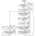
- FIG. 2 is a flowchart of the data reception process of the data recorder 1.
- the input interface 2 attempts to receive the data transmitted from the outside of the data recorder 1 (step S21), and if the data is received from the outside (step S21: YES), the input interface 2 sequentially receives the data.
- the transferred data is transferred to the buffer memory 22, and the transferred data is erased (step S22). If the data is not received from the outside in step S21 (step S21: NO), the attempt to receive the data transmitted from the outside is repeated in step S21. Further, after step S22, the process proceeds to step S21 again.
- FIG. 3 shows a flowchart of the storage process of the data recorder 1.
- the control unit 4 monitors the amount of data stored in the buffer memory 22 by the data amount monitoring unit 42, and determines whether or not the threshold value 400 has been exceeded (step S31). When the amount of data stored in the buffer memory 22 exceeds the threshold value 400 (step S31: YES), the control unit 4 sends the power supply control signal to the power supply control signal receiving unit 34 by the power supply control signal transmitting unit 43, and is non-volatile. The power supply of the power source 33 for sex memory is switched from the off state to the on (step S32).
- the data transmission / reception unit 21 reads the data from the buffer memory 22 and transfers the data to the storage unit 3 (step S33). ). The data transferred to the storage unit 3 is written in the non-volatile memory 32.
- the data amount monitoring unit 42 monitors the amount of data stored in the buffer memory 22 again, and determines whether or not the buffer memory 22 is empty (step S34). If the buffer memory 22 is not empty in step S34 (step S34: NO), that is, if the data stored in the buffer memory 22 remains, the process proceeds to step S33, and the data transfer to the storage unit 3 is repeated. ..
- step S34 If all the data in the buffer memory 22 is transferred and the buffer memory 22 is empty (step S34: YES), the control unit 4 transmits a power control signal to the power control signal receiving unit 34 by the power control signal transmitting unit 43. The power supply of the non-volatile memory power supply 33 is switched off (step S35).
- the data recorder 1 receives data from the outside and stores it in the non-volatile memory 32 by the data reception process and the storage process described above. At that time, the control unit 4 turns on the power supply 33 for the non-volatile memory at a timing determined based on the amount of data recorded in the buffer memory 22, as in steps S31 and S32 of the flowchart of FIG.
- the switching and input interface 2 transfers the data recorded in the non-volatile memory 22 to the non-volatile memory 32 when the power supply 33 for the non-volatile memory is on, and the control unit 4 is recorded in the buffer memory 22. After the transfer of the data to the non-volatile memory 32 is completed, the power supply 33 for the non-volatile memory is switched off.
- the adverse effects of radiation can be suppressed, and the power consumption of the data recorder 1 can be reduced.
- the adverse effect of radiation can be suppressed by turning off the non-volatile memory 32.
- the data recorder 1 can be power-saving.
- FIG. 4 is a flowchart of the reproduction data reading process.
- the reproduction data reading process is a process of reading the reproduction data from the non-volatile memory 32 to the buffer memory 52 for the reproduction process described later. Further, the reproduction data is the data to be output of the data recorder 1, that is, the data to be reproduced, and is, for example, the data designated to be reproduced by the reproduction request command received by the command receiving unit 41.
- step S41 The control unit 4 confirms whether the command receiving unit 41 has received the playback request command (step S41). If there is a reproduction request command received by the command receiving unit 41 (step S41: YES), the process proceeds to step S42. If there is no playback request command received by the command receiving unit 41 (step S41: NO), step S41 is repeated.
- step S42 it is confirmed whether the buffer memory 52 is empty (step S42). If the buffer memory 52 is not empty (step S42: NO), step S42 is repeated until the reproduction of the data remaining in the buffer memory 52 is completed and the buffer memory 52 becomes empty.
- step S42 If the buffer memory 52 is empty (step S42: YES), the control unit 4 transmits a power supply control signal to the power supply control signal receiving unit 34 by the power supply control signal transmitting unit 43, and turns off the power supply of the non-volatile memory power supply 33. To switch on (step S43).
- the data transmission / reception unit 31 included in the storage unit 3 reads the reproduced data from the non-volatile memory 32 of the storage unit 3 and transmits the reproduction data to the data transmission / reception unit 51 provided in the output interface 5 (step S44).
- the data transmission / reception unit 51 writes the reproduction data received from the data transmission / reception unit 31 to the buffer memory 52 (step S45).
- steps S44 and S45 when the amount of regenerated data that has not yet been read from the non-volatile memory 32 is larger than the capacity of the non-volatile memory 32, the regenerated data that can be stored in the non-volatile memory 32 is the non-volatile memory 32. Is read from and transmitted to the buffer memory 52 via the data transmission / reception unit 31 and the data transmission / reception unit 51.
- control unit 4 determines whether all the reproduced data has been read from the non-volatile memory 32 of the storage unit 3 and transmitted to the buffer memory 52 (step S46).
- step S46 If the reading of some of the reproduced data from the non-volatile memory 32 and the transmission to the buffer memory 52 have not been completed (step S46: NO), the process proceeds to step S47.
- step S47 the control unit 4 confirms whether the buffer memory 52 is empty (step S47).
- step S47 NO
- the control unit 4 turns off the power supply 33 for the non-volatile memory (step S48) until the buffer memory 52 becomes empty by the reproduction process described later.
- step S47 is repeated.
- the control unit 4 is switched off by the power control signal transmission unit 43 when the non-volatile memory power supply 33 is originally on, and is turned off when the non-volatile memory power supply 33 is originally off. Leave it as it is.
- step S47 If the buffer memory 52 is empty in step S47 (step S47: YES), the process proceeds to step S43.
- step S46 when all the reproduced data has been read from the non-volatile memory 32 and transmitted to the buffer memory 52 (step S46: YES), the control unit 4 is used for the non-volatile memory by the power supply control signal transmission unit 43.
- the power supply of the power supply 33 is switched from on to off (step S49), and the process proceeds to step S41.
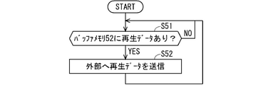
- FIG. 5 is a flowchart of the reproduction process.
- the reproduction process is a process of transmitting the reproduction data read from the non-volatile memory 32 and transmitted to the buffer memory 52 in the reproduction data reading process to the outside via the output interface 5.
- the data transmission / reception unit 51 determines whether or not there is reproduction data in the buffer memory 52 (step S51), and if there is reproduction data in the buffer memory 52 (step S51: YES), the reproduction data in the buffer memory 52 is used. It is transmitted to the outside, and the reproduced data that has been transmitted is erased from the buffer memory 52 (step S52). After step S52, step S51 is repeated.
- step S51 If there is no reproduction data in the buffer memory 52 in step S51 (step S51: NO), step S51 is repeated.
- the data recorder 1 saves the reproduction data stored in the non-volatile memory 32 via the buffer memory 52, that is, once stored in the buffer memory 52 by the reproduction data reading process and the reproduction process described above, and then from the buffer memory 52. Read and output to the outside.
- the control unit 4 has a grace period to turn off the power supply 33 for the non-volatile memory during data reproduction, the control unit 4 starts transferring the reproduced data to the buffer memory 52 in step S48 of the flowchart of FIG.
- the power supply 33 for the non-volatile memory is turned off during a part of the period from the start to the transfer of the reproduced data to the buffer memory 52.
- the control unit 4 powers the non-volatile memory power supply 33 during a part of the period from the start of transfer of the reproduction data to the buffer memory 52 to the end of the transfer of the reproduction data to the buffer memory 52. Turn it off. As a result, the adverse effects of radiation can be suppressed.
- the data recorder 1 is used for the non-volatile memory while executing data input from the outside, instead of controlling the on / off of the power supply 33 for the non-volatile memory in steps S32 and S35.
- the configuration may be such that the power supply 33 is turned on and the power supply 33 for the non-volatile memory is turned off except when data input from the outside is being executed. Even in the data recorder 1 having such a configuration, ⁇ A-3. Effect> The effect described in is obtained.
- step S42 and step S47 the control unit 4 determines whether or not the buffer memory 52 is empty, but instead of determining whether or not the buffer memory 52 is empty, the amount of data stored in the buffer memory 52 is a threshold value ( It may be determined whether or not the value is less than the second threshold value (hereinafter referred to as the threshold value 401).
- the threshold value 401 is, for example, a range in which the buffer memory 52 is not emptied before the non-volatile memory power supply 33 is switched on and reading from the non-volatile memory 32 becomes possible in consideration of the rise time of the non-volatile memory 32. Therefore, it is set as a value as small as possible and stored in the control unit 4.
- the control unit 4 turns off the power supply 33 for the non-volatile memory during a part of the period until the reproduction data is completely transferred to the buffer memory 52.
- the control unit 4 turns off the power supply 33 for the non-volatile memory during a part of the period until the reproduction data is completely transferred to the buffer memory 52.
- steps S42 and S47 if the amount of reproduced data that has not yet been read from the non-volatile memory 32 is equal to or less than the free capacity of the buffer memory 52, the process proceeds to step S43 and the data has not been read yet.
- the reproduction data may be transferred to the buffer memory 52.
- control unit 4 writes to the non-volatile memory 32 and / or writes to the non-volatile memory 32 so that the writing to the non-volatile memory 32 and / or reading from the non-volatile memory 32 during execution is not hindered.
- the power supply 33 for the non-volatile memory is switched off only at the timing when the reading from is not performed.
- step S35 of the flowchart of the storage process shown in FIG. 3 control is performed at the timing when writing to the non-volatile memory 32 and / or reading from the non-volatile memory 32 is performed in a process other than the storage process.
- the unit 4 does not switch off the power supply 33 for the non-volatile memory, and proceeds to step S31.
- the timing at which writing to the non-volatile memory 32 and / or reading from the non-volatile memory 32 in a process other than the storage process is performed is, for example, step S44 of the flowchart of the reproduction data read process shown in FIG. It is the timing when the processing of is being performed.
- step S35 at the timing when the writing to the non-volatile memory 32 and the reading from the non-volatile memory 32 are not performed in the processing other than the storage processing, ⁇ A-2.
- the control unit 4 switches off the power supply 33 for the non-volatile memory and proceeds to step S31.
- the control unit 4 turns off the power supply 33 for the non-volatile memory even at the timing when writing to the non-volatile memory 32 and / or reading from the non-volatile memory 32 is performed in a predetermined situation, and the control unit 4 is determined in advance.
- the power supply 33 for the non-volatile memory may be turned off only at the timing when the writing to the non-volatile memory 32 and the reading from the non-volatile memory 32 are not performed.
- the predetermined situation is, for example, a situation in which a command for forcibly turning off the power supply 33 for the non-volatile memory is received from the outside via the command receiving unit 41.
- the predetermined situation is determined. For example, when the overcurrent of the non-volatile memory power supply 33 is detected, the non-volatile memory power supply 33 is turned off.
- Embodiment 2 In the data recorder 1 of the first embodiment, when the amount of data stored in the buffer memory 22 provided in the input interface 2 exceeds the threshold value, the power supply 33 for the non-volatile memory is changed from off to on.
- the threshold value 400 used in the first embodiment as the threshold value of the amount of data stored in the buffer memory 22 is a fixed value and does not fluctuate. However, when the communication speed at which the data recorder receives or transmits data from the outside is not constant, it is desirable to be able to dynamically change the threshold value from the viewpoint of radiation countermeasures and power saving.
- FIG. 6 is a block diagram showing a configuration of a data recorder 1b, which is a data recorder according to the second embodiment.
- the data recorder 1b is different from the data recorder 1 which is the data recorder according to the first embodiment in that the control unit 4 is the control unit 4b.
- the input interface 2 and the output interface 5 are limited to be able to communicate with the outside at a plurality of communication speeds, but will be described as the input interface 2 and the output interface 5 which are the same interfaces as the first embodiment. ..
- the configuration of the data recorder 1b is the same as that of the data recorder 1b.
- the communication speed with the outside is the speed of data input when data is input to the data recorder 1b from the outside, and the speed of data output when data is output from the data recorder 1b to the outside.
- the data recorder 1b may not only be able to communicate with the outside at a plurality of communication speeds, but may also have a configuration in which the communication speed differs between the input and the output.
- the control unit 4b further includes a threshold control unit 44 as compared with the control unit 4. Similar to the control unit 4 of the first embodiment, the control unit 4b monitors the amount of data stored in the buffer memory 22 by the data amount monitoring unit 42, and when the threshold value 400 is exceeded, the power supply control signal transmission unit 43 transmits a power supply control signal instructing the power supply control signal receiving unit 34 to turn on the power supply 33 for the non-volatile memory. In the present embodiment, the threshold control unit 44 controls the threshold value 400.
- the command indicating the start of communication received by the command receiving unit 41 included in the control unit 4b includes information on the communication speed. Other than that, the configuration of the control unit 4b is the same as that of the control unit 4.
- the communication with low communication speed is defined as low-speed data communication, and the other is defined as high-speed data communication.
- the threshold value 400 is set to be suitable for low-speed data communication, that is, the buffer memory 22 does not overflow and the buffer memory 22 can be fully utilized in the case of low-speed data communication, the threshold value 400 of the same value is used.
- the buffer memory 22 may overflow.
- the threshold value 400 is set to be suitable for high-speed data communication, that is, the buffer memory 22 does not overflow and the buffer memory 22 can be fully utilized in the case of high-speed data communication, the threshold value 400 of the same value is set.
- the buffer memory 22 has free space, that is, the power supply 33 for the non-volatile memory is turned on while there is a grace period for keeping the power supply 33 for the non-volatile memory turned off. Will switch to. That is, there is room to extend the time in which the non-volatile memory power supply 33 is off, and there is room for more effective radiation countermeasures and power saving.
- the storage capacity of the buffer memory 22 is defined as MB [Gbit], and the amount of data stored in the buffer memory 22 is defined as MW [Gbit].
- the rise time of the non-volatile memory 32 is T POW [s]
- the communication speed of the input from the outside is A [Gbps].
- the communication speed A is either the communication speed A0 in high-speed data communication or the communication speed A1 in low-speed data communication, but it is considered that the communication speed A is fixed to either one in a series of communication.
- a 0 and A 1 satisfy A 0 > A 1 .
- TOVR (MB ⁇ MW ) / A.
- MLIM MB ⁇ A ⁇ T POW .
- MB 5 Gbit
- a 0 2 Gbps
- a 1 1 Gbps
- T POW 1s
- the data transfer speed from the buffer memory 22 to the non-volatile memory 32 is the data input from the outside.
- the values given here are examples and can be changed according to the design of the data recorder 1b.
- FIG. 7 shows the variation of MW when the threshold value 400 is M 0 LIM .
- FIG. 8 shows the variation of MW when the threshold value 400 is M 1 LIM .
- the time during which the non-volatile memory power supply 33 is on can be reduced by setting the threshold value 400 to a larger value.
- the threshold value 400 is M 1 LIM
- the buffer memory 22 can be used effectively as compared with the case where the threshold value 400 is M 0 LIM , so that the number of times of switching the power supply 33 for the non-volatile memory 33 can be reduced. You can reduce the amount of time you are on. In the example of FIG. 7, the time that the non-volatile memory power supply 33 is on due to the rise time of the non-volatile memory 32 is 5 seconds out of 25 seconds, but in the example of FIG.
- the non-volatile memory power supply 33 is turned on. Since the number of switchings between and off is reduced, the time that the power supply 33 for the non-volatile memory is on due to the rise time of the non-volatile memory 32 is 4 seconds out of 25 seconds.
- the threshold value of the maximum value is M 0 LIM for high-speed data communication and M 0 LIM for low-speed data communication within the range where the non-volatile memory 32 does not overflow so as not to interfere with data input from the outside. Is M 1 LIM and is different. Therefore, in the data recorder 1b of the present embodiment, the threshold control unit 44 sets the threshold value 400 to M 0 LIM in the case of high-speed data communication and M 0 LIM in the case of low-speed data communication based on the speed of data input from the outside.
- the threshold 400 is set to M 1 LIM .
- the threshold value 400 is set slightly smaller than M 0 LIM or M 1 LIM in consideration of the fluctuation.
- the control unit 4b is based on the amount of data recorded in the buffer memory 22 and the speed of data input from the outside via the input interface 2.
- the power supply 33 for the non-volatile memory is switched on.
- the threshold control unit 44 included in the control unit 4b determines the threshold value 400 based on the speed of data input from the outside, and the control unit 4b is shown in steps S31 and S32 of the flowchart of FIG.
- the power supply 33 for the non-volatile memory is switched on.
- the input interface 2 transfers the data recorded in the non-volatile memory 22 to the non-volatile memory 32 when the power supply 33 for the non-volatile memory is on, and the control unit 4 records the data in the buffer memory 22. After transferring the data to the non-volatile memory 32, the power supply 33 for the non-volatile memory is switched off. With such a configuration, since the time that the non-volatile memory power supply 33 is in the ON state is reduced, the adverse effect of radiation can be further suppressed, and the data recorder 1b can be further reduced in power consumption.
- the adverse effect of radiation can be further suppressed, and the adverse effect of radiation can be further suppressed.
- the data recorder 1b can be further reduced in power consumption.
- the threshold control unit 44 when the power supply 33 for non-volatile memory is turned off from on, it is assumed that the writing to the power supply 33 for non-volatile memory can be turned off instantly after the writing is completed. If it takes time for the power supply 33 for non-volatile memory to turn off after writing to the power supply 33 for non-volatile memory is completed, the threshold control unit 44 also bases the time for that amount on the speed of data input from the outside. By switching the non-volatile memory power supply 33 on at the predetermined timing, it can be reduced as the number of times the non-volatile memory power supply 33 is switched on and off decreases.
- FIGS. 7 and 8 have been described assuming a situation where the data input speed is constant during a series of data input, the data input speed may change during the series of data input.
- the control unit 4b is recorded in the buffer memory 22.
- the change in the data input speed is permitted after the amount of the existing data becomes the threshold value of 400 or less, which is determined based on the changed data input speed.
- the threshold control unit 44 uses the speed of data input from the outside as a command from the outside received by the command receiving unit 41. It can also be obtained by monitoring the information on the included communication speed, the information on the operating status of the data transmission / reception unit 21, and the fluctuation speed of the amount of data stored in the buffer memory 22, and even in these cases, it is practically possible. In addition, it can be said that the threshold control unit 44 controls the threshold 400 based on the speed of data input.
- the control unit 4b turns on the power supply 33 for the non-volatile memory at a timing determined based on the amount of data recorded in the buffer memory 22 and the speed of data input from the outside via the input interface 2. Although described as switching, more generally, it may be based on the mode of data entry rather than the speed of data entry. For example, if it is known from the command received by the command receiving unit 41 that the data is input intermittently at intervals of a certain amount or less, for example, the free space is fixed based on the fixed amount.
- the threshold value 400 may be controlled so that the data is transferred to the non-volatile memory 32 when the amount is less than or equal to the amount.
- the control unit 4b is for the non-volatile memory at a timing determined based on the amount of data recorded in the buffer memory 22 and the speed of data input from the outside via the input interface 2.
- the power supply 33 is switched on, the input interface 2 transfers the data recorded in the buffer memory 22 to the non-volatile memory 32 when the power supply 33 for the non-volatile memory is on, and the control unit 4 transfers the buffer.
- the non-volatile memory power supply 33 is switched off. As a result, the adverse effects of radiation can be suppressed.
- the control unit 4b is, for example, ⁇ A-5.
- the threshold value 401 described in the modification 2> is controlled based on the mode of data output to the outside.
- the threshold control unit 44 sets, for example, the smallest possible threshold value in the threshold value so that the buffer memory 52 does not become empty before the data can be read from the non-volatile memory 32 after step S43, and the mode of data output during execution. For example, it is set according to the speed of data output.
- it is possible to prevent the data output from being hindered by controlling the on / off of the power supply 33 for the non-volatile memory, and to suppress the time during which the power supply 33 for the non-volatile memory is on, which is adversely affected by radiation.
- the power saving of the data recorder 1 can be achieved. In particular, when data reproduction continues for a long time and an amount of data equal to or larger than the capacity of the buffer memory 52 is reproduced, adverse effects due to radiation can be suppressed, and power saving of the data recorder 1 can be achieved.
- the non-volatile memory power supply 33 is turned off when it is not necessary to turn it on, thereby suppressing the frequency of latch-up caused by radiation, for example.
- the data recorder 1c which is the data recorder according to the third embodiment, the current value of the non-volatile memory power supply 33 is monitored as a countermeasure against the occurrence of latch-up, and when an overcurrent is detected, the non-volatile memory power supply 33 is detected. Power is switched off.
- FIG. 9 is a block diagram showing the configuration of the data recorder 1c.
- the data recorder 1c is different from the data recorder 1 which is the data recorder according to the first embodiment in that the control unit 4 is the control unit 4c. Other than that, the configuration of the data recorder 1c is the same as that of the data recorder 1c.
- the control unit 4c further includes a current value monitoring unit 45 as compared with the control unit 4.
- the current value monitoring unit 45 acquires and monitors the current value of the non-volatile memory power supply 33.
- the current value monitoring unit 45 acquires the current value of the non-volatile memory power supply 33 from, for example, an ammeter provided in the non-volatile memory power supply 33.
- a current threshold value (third threshold value, hereinafter, current threshold value 60), which is a safe current value in terms of specifications of the non-volatile memory 32 and the non-volatile memory power supply 33, is recorded in advance. Further, the control unit 4c is described in ⁇ C-2. The process for detecting latch-up and preventing failure or suppressing the frequency of failure, as described in Operation>, is performed.
- the control unit 4c has the same configuration as the control unit 4 except that the control unit 4c has the same configuration as the control unit 4.
- the control unit 4c is further provided with the current value monitoring unit 45 as compared with the control unit 4, but the control unit 4c is further provided with the current value monitoring unit 45 as compared with the control unit 4b, and the data recorder 1c is ⁇ B-2.
- the same operation as the operation> may be performed.
- the data recorder 1c is the same as the data recorder 1 ⁇ A-2. Operation> is performed. However, ⁇ A-2. In the description of operation>, the control unit 4 is read as the control unit 4c.
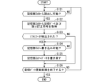
- FIG. 10 is a flowchart showing a process for the data recorder 1c to detect latch-up and prevent a failure or suppress the frequency of failures.
- the current value monitoring unit 45 acquires the value of the current flowing through the non-volatile memory power supply 33 when the power of the non-volatile memory power supply 33 is turned on (step S101).
- the value of the current flowing through the non-volatile memory power supply 33 measured by the current value monitoring unit 45 is hereinafter referred to as a measured current value.
- the current value monitoring unit 45 determines whether the measured current value exceeds the current threshold value 60 (step S102). If the measured current value does not exceed the current threshold value 60, that is, if no overcurrent is detected (step S102: NO), the process proceeds to step S103.
- step S103 the control unit 4c confirms whether the state of the non-volatile memory power supply 33 is on, and if the non-volatile memory power supply 33 is in the off state (step S103: NO), it is shown in FIG. Ends the operation of the flow chart. If the non-volatile memory power supply 33 is in the ON state in step S103 (step S103: YES), the process proceeds to step S101.
- the current value monitoring unit 45 sets the current threshold value 60 for the value of the current flowing through the non-volatile memory power supply 33 while the non-volatile memory power supply 33 is on. Continue to monitor for excess.
- step S102 when the current value monitoring unit 45 determines that the measured current value exceeds the current threshold value 60, that is, when an overcurrent is detected (step S102: YES), the control unit 4c is the power supply control signal transmission unit.
- the power supply 33 for the non-volatile memory is switched off by 43 (step S104).
- the non-volatile memory power supply 33 includes a plurality of power supply devices and the plurality of power supply devices each supply power to the non-volatile memory 32, only the power supply device in which an abnormality is detected is switched off. May be good.
- step S104 When the non-volatile memory power supply 33 is turned off in step S104, the operation of the flowchart shown in FIG. 10 ends.
- control unit 4c switches off the power supply of the non-volatile memory power supply 33 at the timing determined by the current value monitoring unit 45 based on the measured current value. Specifically, when the measured current value exceeds the current threshold value 60, the power supply of the non-volatile memory power supply 33 is switched off. As a result, it is possible to detect the occurrence of latch-up that may occur when the non-volatile memory power supply 33 is on, and prevent the data recorder 1c from failing due to the latch-up or suppress the frequency of failures.
- the control unit 4c includes a current value monitoring unit 45, and the control unit 4c turns off the power supply of the non-volatile memory power supply 33 at a timing determined by the current value monitoring unit 45 based on the measured current value. Switch.
- the data recorder 1c can detect the occurrence of latch-up and prevent the data recorder 1c from failing due to the latch-up or suppress the frequency of failures.
- Embodiment 4 The data recorder 1, the data recorder 1b, and the data recorder 1c described in the first to third embodiments suppress the occurrence of upset and latch-up by switching the power supply 33 for the non-volatile memory on and off. Was.
- the data recorder 1d which is the data recorder according to the present embodiment, suppresses the occurrence of uncorrectable soft errors by reading the data and writing back the corrected data.
- FIG. 11 is a block diagram showing the configuration of the data recorder 1d.
- the lines representing the operations of the command receiving unit 41, the data amount monitoring unit 42, and the power supply control signal transmitting unit 43 are omitted.
- the data recorder 1d is different from the data recorder 1 which is the data recorder according to the first embodiment in that the storage unit 3 is the storage unit 3d and the control unit 4 is the control unit 4d. Other than that, the configuration of the data recorder 1d is the same as that of the data recorder 1d.
- the non-volatile memory 32 is a non-volatile memory 32d as compared with the storage unit 3. In other respects, the storage unit 3d is the same as the storage unit 3.
- the non-volatile memory 32d When storing the data, the non-volatile memory 32d also stores the error correction code of the data.
- the error correction code may be stored in a memory other than the non-volatile memory 32. Further, the error correction code may be of any format as long as the error of the data stored in the non-volatile memory 32 can be corrected.
- the control unit 4d further includes a storage data update unit 46 as compared with the control unit 4.
- the storage data update unit 46 is described in ⁇ D-2. Perform the storage data update process described in Operation>. Other than that, the configuration of the control unit 4d is the same as that of the control unit 4.
- control unit 4d has been described as further including a storage data update unit 46 as compared with the control unit 4, the control unit 4d may further include a current value monitoring unit 45 as compared with the control unit 4b or the control unit 4c.
- data recorder 1d is ⁇ B-2. Operation> or ⁇ C-2. Operation> or both may be performed in the same manner.
- the data recorder 1d is the same as the data recorder 1 ⁇ A-2. Operation> is performed. However, ⁇ A-2.
- the storage unit 3 is read as a storage unit 3d
- the non-volatile memory 32 is read as a non-volatile memory 32d
- the control unit 4 is read as a control unit 4d.
- the storage data update unit 46 determines whether or not there is a margin for reading data from the non-volatile memory 32 based on the access status of writing and reading to the non-volatile memory 32, and the non-volatile memory 32 has a margin for reading. Occasionally, the stored data, which is the data stored in the non-volatile memory 32, is read from the non-volatile memory 32. At this time, the error correction code of the stored data is also acquired, and the presence or absence of a soft error in the stored data is determined. If no soft error is detected, it is not necessary to write back to the non-volatile memory 32. When a soft error is detected, the data corrected by the soft error is written back to the non-volatile memory 32 when there is a margin for writing in the access status of the non-volatile memory 32.
- the data stored in the non-volatile memory 32 is read from the non-volatile memory 32, and if a soft error occurs, the data after the soft error correction is written back to the non-volatile memory 32.
- the storage data update process it is possible to prevent or suppress the frequency of soft errors that exceed the correction capability of the error correction code and prevent the errors from being corrected in the stored data of the non-volatile memory 32, and the non-volatile memory is non-volatile.
- the reliability of the data stored in the sex memory 32 can be improved.
- the determination of whether or not there is a margin for reading data or writing data for example, it can be determined that there is a margin when the power supply 33 for the non-volatile memory is off. However, it may be determined whether or not the data can be read or the data can be written by another method. Further, in order to allow the non-volatile memory 32 to have a margin for reading or writing data, the data transfer rate between the buffer memory 22 or the buffer memory 52 and the non-volatile memory 32 may be lowered.
- the operation procedure of the stored data updating unit 46 in the data recorder 1d according to the fourth embodiment described above will be described according to the flowchart shown in FIG.
- the operation of the storage data updating unit 46 starts the operation of the flowchart shown in FIG. 12, for example, periodically or by a command via the user's command receiving unit 41.
- the storage data update unit 46 first confirms whether the non-volatile memory 32 has a margin for reading, that is, whether it can be read (step S121). If it is not readable (step S121: NO), step S121 is repeated, and the confirmation work is continued until readable.
- the storage data update unit 46 reads the storage data of a predetermined size from the non-volatile memory 32, and corrects the error in the read storage data.
- the code is also acquired (step S122).
- the predetermined size may be an arbitrarily set size.
- the control unit 4e turns on the non-volatile memory power supply 33 by the power control signal transmission unit 43, and then the storage data update unit 46 is non-volatile. Read data from the non-volatile memory 32.
- the storage data update unit 46 determines the presence or absence of a soft error based on the read storage data and the acquired error correction code (step S123). As a result, if no soft error is detected (step S123: NO), it is not necessary to rewrite the data read in step S122 to the non-volatile memory 32, so the process proceeds to step S126.
- step S123 If a soft error is detected in step S123 (step S123: YES), the read data needs to be written again to the non-volatile memory 32 after the soft error is corrected, so that the storage data update unit 46 performs the non-volatile memory 32. Check if it is writable to (step S124).
- step S124 If it is not writable to the non-volatile memory 32 (step S124: NO), the storage data update unit 46 repeats step S124 until it becomes writable, and continues the confirmation work.
- step S124 When the data can be written to the non-volatile memory 32 (step S124: YES), the storage data update unit 46 writes back the data after the soft error correction to the non-volatile memory 32 (step S125), and after the writing is completed, the data is written back to the non-volatile memory 32. The process proceeds to step S126.
- step S126 the storage data update unit 46 determines whether or not to end the storage data update process. For example, if all the update processing for the data stored in the non-volatile memory 32 at the start of the storage data update processing is completed, the process ends, and if not, the process returns to step S121.
- step S126 when the storage data update process is completed, if the data is not reproduced or recorded, the control unit 4e turns off the power supply 33 for the non-volatile memory by the power supply control signal transmission unit 43, and then the control unit 4e turns off the power supply 33 for the non-volatile memory. The storage data update process is completed.
- the storage data update unit 46 performs the storage data update process.
- the storage data update unit 46 performs the storage data update process.
- Embodiment 5 In the data recorder 1d according to the fourth embodiment, for example, by periodically reading out the stored data, detecting an error, and writing back the corrected data, an error can be obtained even if an error correction code is used. Was prevented from becoming uncorrectable. However, the frequency of soft errors caused by upsets and the like depends on the environment. Therefore, it is desirable that the frequency of reading the data, detecting the error, writing back the error-corrected data, and performing the storage data update process can be dynamically changed.
- the data recorder 1e which is a data recorder according to the present embodiment, monitors the frequency of soft error occurrence and dynamically changes the frequency of the stored data update process to suppress the execution of unnecessary stored data update process. In addition, it suppresses the occurrence of errors that cannot be corrected due to changes in the environment.
- FIG. 13 is a block diagram showing the configuration of the data recorder 1e.
- the lines representing the operations of the command receiving unit 41, the data amount monitoring unit 42, and the power supply control signal transmitting unit 43 are omitted.
- the data recorder 1e includes a control unit 4e instead of the control unit 4d as compared with the data recorder 1d according to the fourth embodiment. Other than that, the configuration of the data recorder 1e is the same as the configuration of the data recorder 1d.
- the control unit 4e further includes a storage data update plan determination unit 47 as compared with the control unit 4d.
- the configuration of the control unit 4e is the same as the configuration of the control unit 4d.
- the storage data update plan determination unit 47 obtains error information regarding the occurrence mode of the soft error obtained in the storage data update process from the storage data update unit 46, for example, the number of detected errors or the number of errors per data amount. get.
- the storage data update plan determination unit 47 determines an update plan, which is a plan for the storage data update process, based on the mode in which a soft error occurs, and the storage data update unit 47 determines the storage data update process based on the update plan. Instruct 46.
- the number of errors that can be corrected for a certain amount of data is usually determined by the format of the error correction code.
- the maximum value of the number of errors that can be corrected for a certain amount of data is Nemax .
- the storage data update plan determination unit 47 specifically determines the plan for the storage data update process by, for example, the following operation.
- the storage data update plan determination unit 47 acquires the number of errors detected in the storage data update process from the storage data update unit 46, and calculates the average value Nave of the number of occurrences per certain amount of data.
- the average value Nave is, for example, the average of the most recent one-time or multiple-time storage data update processing.
- the storage data update plan determination unit 47 determines, for example, a predetermined ratio of the Nave value expected in the next storage data update process to Nemax when it is assumed that the number of errors generated per hour does not change.
- the frequency of storage data update processing should be as low as possible within the range of the following values. As a result, assuming that the environment changes more slowly than the storage data update processing interval, if many soft errors occur, it will occur every time the storage data update processing is performed by increasing the frequency of the storage data update processing. If the expected value of the number of uncorrectable errors is preferably kept below a certain level and soft errors rarely occur, unnecessary storage data update processing can be omitted.
- the predetermined ratio can be arbitrarily set as a design value, but may be specified by the user via the command receiving unit 41.
- the stored data is kept below a certain value so that the expected value of the number of uncorrectable errors that occur per hour is kept below a certain value.
- the frequency of update processing may be determined.
- the storage data update plan determination unit 47 may, for example, use the time interval between the storage data update processes. The maximum value of may be set.
- the minimum value of the time interval between the storage data update processes is set. And so on.
- the stored data update plan determination unit 47 determines a plan for the stored data update process based on the mode of occurrence of the soft error detected in the stored data update process. As a result, the reliability of the data stored in the non-volatile memory 32 can be improved, and the time during which the non-volatile memory power supply 33 is on can be suppressed, for example, the occurrence of latch-up can be suppressed.
- Embodiment 6 In the present embodiment, the hardware configuration of the data recorders 1 to the data recorders 1e described in the first to fifth embodiments will be described.
- FIG. 14 is a diagram showing the hardware configurations of the data transmission / reception unit 21, the data transmission / reception unit 31, the data transmission / reception unit 51, the power supply control signal reception unit 34, and the control units 4, 4b, 4c, 4d, 4e.
- the buffer memories 22, 52, the non-volatile memory 32, the non-volatile memory power supply 33, and the like are not shown.
- Each function of the data transmission / reception unit 21, the data transmission / reception unit 31, the data transmission / reception unit 51, the power supply control signal reception unit 34, and the control units 4, 4b, 4c, 4d, 4e is realized by the processing circuit HW1.
- Each function of the update unit 46 and the storage data update plan determination unit 47 is realized by the processing circuit HW1.
- the processing circuit HW1 may be dedicated hardware or a CPU (central processing unit) that executes a program stored in the memory HW2.
- the processing circuit HW1 may be, for example, a single circuit, a composite circuit, a programmed processor, a parallel programmed processor, an ASIC (Application Specific Integrated Circuit), or an FPGA (Field-Programmable). Gate Array) or a combination of these is applicable.
- the functions of the data transmission / reception unit 21, the data transmission / reception unit 31, the data transmission / reception unit 51, the power supply control signal reception unit 34, and the control units 4, 4b, 4c, 4d, and 4e are software and firmware. , Or a combination of software and firmware. Software and firmware are described as programs and stored in the memory HW2.
- the processing circuit HW1 reads and executes the program stored in the memory HW2 to read and execute the data transmission / reception unit 21, the data transmission / reception unit 31, the data transmission / reception unit 51, the power supply control signal reception unit 34, and the control units 4, 4b, 4c. , 4d, 4e functions are realized.
- the functions of the data transmission / reception unit 21, the data transmission / reception unit 31, the data transmission / reception unit 51, the power supply control signal reception unit 34, and the control units 4, 4b, 4c, 4d, and 4e are partially realized by dedicated hardware. The rest may be implemented in software or firmware.
- the memory HW2 is, for example, a non-volatile semiconductor memory such as a flash memory, an MRAM, or an EEPROM, any one of a magnetic disk, a flexible disk, an optical disk, a compact disk, a mini disk, a DVD, or a combination thereof.
- the memory HW2 is, for example, a memory different from the buffer memory 22, the buffer memory 52, and the non-volatile memory 32, but the memory HW2 may be the buffer memory 22 or the non-volatile memory 32.
- FIG. 15 is a data recorder 100 of the present embodiment.
- the data recorder 100 includes an input interface 200, a storage unit 300, and a control unit 4000.
- the storage unit 300 includes a non-volatile memory 32 for storing data and a non-volatile memory power supply 33 which is a power supply for the non-volatile memory 32 and whose on / off control is controlled by the control unit 4000.
- the input interface 200 includes a buffer memory 22 which is a first buffer memory.
- the input interface 200 receives data input from the outside and records it in the buffer memory 22.
- the control unit 4000 turns on the power supply 33 for the non-volatile memory at a timing determined based on the amount of data recorded in the buffer memory 22 and the mode of data input from the outside via the input interface 200.
- the switching and input interface 200 transfers the data recorded in the non-volatile memory 22 to the non-volatile memory 32 when the power supply 33 for the non-volatile memory is on, and the control unit 4000 is recorded in the buffer memory 22. After transferring the data to the non-volatile memory 32, the power supply 33 for the non-volatile memory is switched off. As a result, the data recorder 100 can suppress the adverse effects of radiation.
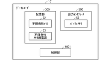
- FIG. 16 is a data recorder 101 of the present embodiment.
- the data recorder 101 includes an output interface 500, a storage unit 300, and a control unit 4001.
- the storage unit 300 includes a non-volatile memory 32 for storing data and a non-volatile memory power supply 33 which is a power supply for the non-volatile memory 32 and whose on / off control is controlled by the control unit 4001.
- the output interface 500 includes a buffer memory 52 which is a second buffer memory.
- the control unit 4001 When the output target data stored in the non-volatile memory 32 is output to the outside via the buffer memory 52, the control unit 4001 starts transferring the output target data to the buffer memory 52 and then outputs the output target.
- the non-volatile memory power supply 33 is turned off during a part of the period until the data is transferred to the buffer memory 52. As a result, the data recorder 101 can suppress the adverse effects of radiation.
- FIG. 17 is a data recorder 102 of the present embodiment.
- the data recorder 102 includes an input interface 200, an output interface 500, a storage unit 300, and a control unit 4002.
- the storage unit 300 includes a non-volatile memory 32 for storing data and a non-volatile memory power supply 33 which is a power supply for the non-volatile memory 32 and whose on / off control is controlled by the control unit 4002.
- the input interface 200 includes a buffer memory 22 which is a first buffer memory.
- the output interface 500 includes a buffer memory 52 which is a second buffer memory.
- the input interface 200 receives data input from the outside and records it in the buffer memory 22.
- the control unit 4002 turns on the power supply 33 for the non-volatile memory at a timing determined based on the amount of data recorded in the buffer memory 22 and the mode of data input from the outside via the input interface 200.
- the switching and input interface 200 transfers the data recorded in the non-volatile memory 22 to the non-volatile memory 32 when the power supply 33 for the non-volatile memory is on, and the control unit 4002 is recorded in the buffer memory 22. After transferring the data to the non-volatile memory 32, the power supply 33 for the non-volatile memory is switched off.
- the data recorder 102 can thereby suppress the adverse effects of radiation.
- the control unit 4002 When the output target data stored in the non-volatile memory 32 is output to the outside via the buffer memory 52, the control unit 4002 starts transferring the output target data to the buffer memory 52 and then outputs the output target.
- the non-volatile memory power supply 33 is turned off during a part of the period until the data is transferred to the buffer memory 52.
- the data recorder 102 can thereby suppress the adverse effects of radiation.
- Embodiment 8> In the present embodiment, how to use the data recorder 1, the data recorder 1b, the data recorder 1c, the data recorder 1d, the data recorder 1e, the data recorder 100, the data recorder 101, and the data recorder 102, respectively, described in the first to sixth embodiments. Will be explained.
- the data recorder 1, the data recorder 1b, the data recorder 1c, the data recorder 1d, the data recorder 1e, the data recorder 100, the data recorder 101, and the data recorder 102 described in the first to fifth embodiments each have a power supply 33 for a non-volatile memory. It is a data recorder with improved radiation resistance by providing a period to turn it off.
- the radiation environment refers to an environment in which the radiation dose is sufficiently higher than the natural environment on the ground, for example, an environment having a radiation dose equivalent to 50 millisieverts or more per year, and the radiation environment is realized in space, for example.
- a radiation environment can be realized on the ground, for example, at a nuclear power plant.
- a data recorder place one of the data recorders in a radiation environment and record the data in either of the data recorders or replay the data recorded in either of the data recorders. This makes it possible to record or reproduce data more stably in a radiation environment. For example, in an observation satellite, a recording request to a data recorder always occurs in a radiation environment, but even in such a case, the data recorder 1 (excluding the configuration of ⁇ A-4.
- Modification 1> and the data recorder.
- the adverse effect of radiation can be suppressed and data can be recorded stably.
Landscapes
- Engineering & Computer Science (AREA)
- Theoretical Computer Science (AREA)
- Physics & Mathematics (AREA)
- General Engineering & Computer Science (AREA)
- General Physics & Mathematics (AREA)
- Quality & Reliability (AREA)
- Techniques For Improving Reliability Of Storages (AREA)
Abstract
To provide a data recorder capable of suppressing an adverse effect caused by radiation. The data recorder of the present disclosure comprises, in one aspect, an input interface including a first buffer memory. The input interface receives data input from the outside and records the data input in the first buffer memory. A control unit implements switching to turn on a nonvolatile-memory power supply at a timing that is determined on the basis of the amount of data recorded in the first buffer memory and the mode of the data input from the outside via the input interface. The input interface transfers, to a nonvolatile memory, the data recorded in the first buffer memory in a case of a state where the nonvolatile-memory power supply is turned on. The control unit implements switching to turn off the nonvolatile-memory power supply after the data recorded in the first buffer memory is transferred to the nonvolatile memory.
Description
本開示はデータレコーダおよびデータレコーダの使用方法に関するものである。
This disclosure relates to a data recorder and how to use the data recorder.
放射線と呼ばれる高いエネルギーを持つ粒子は電子機器に悪影響を与えることが知られている。放射線は、宇宙空間において飛び交っている他、地上においても、宇宙からくる放射線や放射性物質から発せられる放射線が存在する。
It is known that particles with high energy called radiation have an adverse effect on electronic devices. In addition to flying around in outer space, radiation also exists on the ground, including radiation coming from space and radiation emitted from radioactive substances.
電子機器またはその一部分の電源をオフとすることにより、当該電子機器またはその当該一部分に対する放射線の悪影響を抑制できる。
By turning off the power of the electronic device or a part thereof, the adverse effect of radiation on the electronic device or a part thereof can be suppressed.
特許文献1には、データレコーダにおいて、省電力を実現するために、データレコーダの不揮発性メモリモジュールの電源を制御する構成が、開示されている。しかし、特許文献1に開示されている電源の制御は、放射線の悪影響への対策の観点から改善の余地があった。
Patent Document 1 discloses a configuration in which a data recorder controls the power supply of the non-volatile memory module of the data recorder in order to realize power saving. However, the power supply control disclosed in Patent Document 1 has room for improvement from the viewpoint of countermeasures against adverse effects of radiation.
本開示は、このような問題を解決するためのものであり、放射線による悪影響を抑制できるデータレコーダを提供すること、および放射線による悪影響を抑制できるデータレコーダの使用方法を提供することを目的としている。
The present disclosure is to solve such a problem, and an object of the present invention is to provide a data recorder capable of suppressing adverse effects of radiation, and to provide a method of using a data recorder capable of suppressing adverse effects of radiation. ..
本開示の一態様のデータレコーダは、入力インタフェースと記憶部と制御部とを備え、記憶部はデータを記憶する不揮発性メモリと不揮発性メモリ用の電源であって制御部にオンとオフを制御される不揮発性メモリ用電源とを備え、入力インタフェースは第1のバッファメモリを備え、入力インタフェースは外部からのデータ入力を受け付けて第1のバッファメモリに記録し、制御部は、第1のバッファメモリに記録されているデータの量と、入力インタフェースを介した外部からのデータ入力の態様と、に基づいて決めたタイミングで、不揮発性メモリ用電源をオンに切り替え、入力インタフェースは、不揮発性メモリ用電源がオンの状態の場合に、第1のバッファメモリに記録されているデータを不揮発性メモリに転送し、制御部は、第1のバッファメモリに記録されているデータを不揮発性メモリに転送した後に、不揮発性メモリ用電源をオフに切り替える、データレコーダ、である。
The data recorder of one aspect of the present disclosure includes an input interface, a storage unit, and a control unit, and the storage unit is a non-volatile memory for storing data and a power supply for the non-volatile memory, and the control unit controls on and off. The input interface is provided with a first buffer memory, the input interface receives data input from the outside and records it in the first buffer memory, and the control unit is a first buffer. The power supply for the non-volatile memory is switched on at the timing determined based on the amount of data recorded in the memory and the mode of data input from the outside via the input interface, and the input interface is the non-volatile memory. When the power is on, the data recorded in the first buffer memory is transferred to the non-volatile memory, and the control unit transfers the data recorded in the first buffer memory to the non-volatile memory. After that, it is a data recorder that switches off the power supply for non-volatile memory.
また、本開示の別の一態様のデータレコーダは、出力インタフェースと記憶部と制御部とを備え、記憶部はデータを記憶する不揮発性メモリと不揮発性メモリ用の電源であって制御部にオンとオフを制御される不揮発性メモリ用電源とを備え、出力インタフェースは第2のバッファメモリを備え、制御部は、不揮発性メモリが記憶している出力対象のデータを第2のバッファメモリを介して外部へ出力する際に、出力対象のデータの第2のバッファメモリへの転送を開始してから出力対象のデータを第2のバッファメモリへ転送し終わるまでの間の期間のうちの一部の期間に、不揮発性メモリ用電源をオフの状態とする、データレコーダ、である。
Further, another aspect of the data recorder of the present disclosure includes an output interface, a storage unit, and a control unit, and the storage unit is a non-volatile memory for storing data and a power supply for the non-volatile memory, and is turned on to the control unit. The output interface is provided with a second buffer memory, and the control unit transfers the data to be output stored in the non-volatile memory via the second buffer memory. Part of the period from the start of transfer of the data to be output to the second buffer memory to the end of transfer of the data to be output to the second buffer memory when outputting to the outside. This is a data recorder that turns off the power supply for non-volatile memory during the period of.
また、本開示のさらに別の一態様のデータレコーダは、入力インタフェースと出力インタフェースと記憶部と制御部とを備え、記憶部はデータを記憶する不揮発性メモリと不揮発性メモリ用の電源であって制御部にオンとオフを制御される不揮発性メモリ用電源とを備え、入力インタフェースは第1のバッファメモリを備え、出力インタフェースは第2のバッファメモリを備え、入力インタフェースは外部からのデータ入力を受け付けて第1のバッファメモリに記録し、制御部は、第1のバッファメモリに記録されているデータの量と、入力インタフェースを介した外部からのデータ入力の態様と、に基づいて決めたタイミングで、不揮発性メモリ用電源をオンに切り替え、入力インタフェースは、不揮発性メモリ用電源がオンの状態の場合に、第1のバッファメモリに記録されているデータを不揮発性メモリに転送し、制御部は、第1のバッファメモリに記録されているデータを不揮発性メモリに転送した後に、不揮発性メモリ用電源をオフに切り替え、制御部は、不揮発性メモリが記憶している出力対象のデータを第2のバッファメモリを介して外部へ出力する際に、出力対象のデータの第2のバッファメモリへの転送を開始してから出力対象のデータを第2のバッファメモリへ転送し終わるまでの間の期間のうちの一部の期間に、不揮発性メモリ用電源をオフの状態とする、データレコーダ、である。
Further, the data recorder of still another aspect of the present disclosure includes an input interface, an output interface, a storage unit, and a control unit, and the storage unit is a non-volatile memory for storing data and a power supply for the non-volatile memory. The control unit is equipped with a power supply for non-volatile memory that can be turned on and off, the input interface is equipped with a first buffer memory, the output interface is equipped with a second buffer memory, and the input interface receives data input from the outside. The timing is determined based on the amount of data recorded in the first buffer memory and the mode of data input from the outside via the input interface. Then, the power supply for the non-volatile memory is switched on, and the input interface transfers the data recorded in the first buffer memory to the non-volatile memory when the power supply for the non-volatile memory is on, and the control unit. Transfers the data recorded in the first buffer memory to the non-volatile memory, then switches off the power supply for the non-volatile memory, and the control unit transfers the data to be output stored in the non-volatile memory to the first. When outputting to the outside via the second buffer memory, between the start of transfer of the data to be output to the second buffer memory and the end of transfer of the data to be output to the second buffer memory. A data recorder that turns off the power supply for non-volatile memory during a part of the period.
また、本開示の一態様のデータレコーダの使用方法は、本開示のデータレコーダを使用する方法であるデータレコーダの使用方法であって、放射線環境にデータレコーダを配置して、データレコーダにデータを記録またはデータレコーダに記録されたデータを再生する、データレコーダの使用方法、である。
Further, the method of using the data recorder in one aspect of the present disclosure is a method of using the data recorder, which is a method of using the data recorder of the present disclosure, in which the data recorder is placed in the radiation environment and the data is stored in the data recorder. How to use a data recorder to replay data recorded or recorded in a data recorder.
本開示の一態様のデータレコーダにおいて、制御部は、第1のバッファメモリに記録されているデータの量と、入力インタフェースを介した外部からのデータ入力の態様と、に基づいて決めたタイミングで、不揮発性メモリ用電源をオンに切り替え、入力インタフェースは、不揮発性メモリ用電源がオンの状態の場合に、第1のバッファメモリに記録されているデータを不揮発性メモリに転送し、制御部は、第1のバッファメモリに記録されているデータを不揮発性メモリに転送した後に、不揮発性メモリ用電源をオフに切り替える。これにより、放射線による悪影響を抑制できるデータレコーダが提供される。
In the data recorder of one aspect of the present disclosure, the control unit has a timing determined based on the amount of data recorded in the first buffer memory and the mode of data input from the outside via the input interface. , The power supply for non-volatile memory is switched on, the input interface transfers the data recorded in the first buffer memory to the non-volatile memory when the power supply for non-volatile memory is on, and the control unit After transferring the data recorded in the first buffer memory to the non-volatile memory, the power supply for the non-volatile memory is switched off. This provides a data recorder capable of suppressing the adverse effects of radiation.
また、本開示の別の一態様のデータレコーダにおいて、制御部は、不揮発性メモリが記憶している出力対象のデータを第2のバッファメモリを介して外部へ出力する際に、出力対象のデータの第2のバッファメモリへの転送を開始してから出力対象のデータを第2のバッファメモリへ転送し終わるまでの間の期間のうちの一部の期間に、不揮発性メモリ用電源をオフの状態とする。これにより、放射線による悪影響を抑制できるデータレコーダが提供される。
Further, in another aspect of the data recorder of the present disclosure, when the control unit outputs the data to be output stored in the non-volatile memory to the outside via the second buffer memory, the control unit outputs the data to be output. The power for the non-volatile memory is turned off during a part of the period from the start of the transfer to the second buffer memory to the end of the transfer of the data to be output to the second buffer memory. Make it a state. This provides a data recorder capable of suppressing the adverse effects of radiation.
また、本開示のさらに別の一態様のデータレコーダにおいて、制御部は、第1のバッファメモリに記録されているデータの量と、入力インタフェースを介した外部からのデータ入力の態様と、に基づいて決めたタイミングで、不揮発性メモリ用電源をオンに切り替え、入力インタフェースは、不揮発性メモリ用電源がオンの状態の場合に、第1のバッファメモリに記録されているデータを不揮発性メモリに転送し、制御部は、第1のバッファメモリに記録されているデータを不揮発性メモリに転送した後に、不揮発性メモリ用電源をオフに切り替え、制御部は、不揮発性メモリが記憶している出力対象のデータを第2のバッファメモリを介して外部へ出力する際に、出力対象のデータの第2のバッファメモリへの転送を開始してから出力対象のデータを第2のバッファメモリへ転送し終わるまでの間の期間のうちの一部の期間に、不揮発性メモリ用電源をオフの状態とする。これにより、放射線による悪影響を抑制できるデータレコーダが提供される。
Further, in still another aspect of the data recorder of the present disclosure, the control unit is based on the amount of data recorded in the first buffer memory and the aspect of data input from the outside via the input interface. At the determined timing, the power supply for the non-volatile memory is switched on, and the input interface transfers the data recorded in the first buffer memory to the non-volatile memory when the power supply for the non-volatile memory is on. Then, after transferring the data recorded in the first buffer memory to the non-volatile memory, the control unit switches off the power supply for the non-volatile memory, and the control unit is the output target stored in the non-volatile memory. When the data of The power for the non-volatile memory is turned off during a part of the period up to. This provides a data recorder capable of suppressing the adverse effects of radiation.
また、本開示の一態様のデータレコーダの使用方法は、本開示のデータレコーダを使用する方法であるデータレコーダの使用方法であって、放射線環境にデータレコーダを配置して、データレコーダにデータを記録またはデータレコーダに記録されたデータを再生する、データレコーダの使用方法、である。これにより、放射線による悪影響を抑制できるデータレコーダの使用方法が提供される。
Further, the method of using the data recorder in one aspect of the present disclosure is a method of using the data recorder, which is a method of using the data recorder of the present disclosure, in which the data recorder is placed in the radiation environment and the data is stored in the data recorder. How to use a data recorder to replay data recorded or recorded in a data recorder. This provides a method of using a data recorder that can suppress the adverse effects of radiation.
また、本願明細書に開示される技術に関連する目的と、特徴と、局面と、利点とは、以下に示される詳細な説明と添付図面とによって、さらに明白となる。
Further, the objectives, features, aspects, and advantages related to the technology disclosed in the present specification will be further clarified by the detailed description and the accompanying drawings shown below.
<A.実施の形態1>
<A-1.構成>
図1は実施の形態1に係るデータレコーダであるデータレコーダ1の構成を示すブロック図である。 <A.Embodiment 1>
<A-1. Configuration>
FIG. 1 is a block diagram showing a configuration of adata recorder 1 which is a data recorder according to the first embodiment.
<A-1.構成>
図1は実施の形態1に係るデータレコーダであるデータレコーダ1の構成を示すブロック図である。 <A.
<A-1. Configuration>
FIG. 1 is a block diagram showing a configuration of a
データレコーダ1は入力インタフェース2と記憶部3と制御部4と出力インタフェース5を備える。
The data recorder 1 includes an input interface 2, a storage unit 3, a control unit 4, and an output interface 5.
入力インタフェース2はデータ送受信部21とバッファメモリ22(第1のバッファメモリ)とを備える。
The input interface 2 includes a data transmission / reception unit 21 and a buffer memory 22 (first buffer memory).
入力インタフェース2はデータレコーダ1の外部から送信されるデータを受信し、当該データを記憶部3へ転送する。
The input interface 2 receives data transmitted from the outside of the data recorder 1 and transfers the data to the storage unit 3.
入力インタフェース2は外部から受信したデータをバッファメモリ22に一時保存する。外部から受信したデータをバッファメモリ22に一時保存することで、後述するように記憶部3が備える不揮発性メモリ用電源33をオフにする猶予が生まれる。
The input interface 2 temporarily stores the data received from the outside in the buffer memory 22. By temporarily storing the data received from the outside in the buffer memory 22, there is a grace period for turning off the power supply 33 for the non-volatile memory provided in the storage unit 3 as described later.
記憶部3はデータ送受信部31と不揮発性メモリ32と不揮発性メモリ用電源33と電源制御信号受信部34を備える。データ送受信部31は入力インタフェース2から転送されるデータを受信し、不揮発性メモリ32へ格納する。また、データの再生時は不揮発性メモリ32からデータを読み込み、当該データを出力インタフェース5へ転送する。
The storage unit 3 includes a data transmission / reception unit 31, a non-volatile memory 32, a power supply 33 for the non-volatile memory, and a power supply control signal reception unit 34. The data transmission / reception unit 31 receives the data transferred from the input interface 2 and stores it in the non-volatile memory 32. Further, when the data is reproduced, the data is read from the non-volatile memory 32 and the data is transferred to the output interface 5.
不揮発性メモリ32は、例えばフラッシュメモリ、MRAM、EEPROM等の、不揮発性の半導体メモリである。
The non-volatile memory 32 is a non-volatile semiconductor memory such as a flash memory, an MRAM, or an EEPROM.
不揮発性メモリ用電源33は不揮発性メモリ32へ電力を供給する電源であり、電源制御信号受信部34から転送される電源の制御信号によって、オンとオフが切り替わる。
The power supply 33 for the non-volatile memory is a power supply that supplies power to the non-volatile memory 32, and is switched on and off by the control signal of the power supply transferred from the power supply control signal receiving unit 34.
電源制御信号受信部34は制御部4から送信される電源制御信号を受信し、不揮発性メモリ用電源33へ受信した電源制御信号を転送する。制御部4は、このように、電源制御信号受信部34を介して、不揮発性メモリ用電源33のオンとオフを制御する。
The power supply control signal receiving unit 34 receives the power supply control signal transmitted from the control unit 4, and transfers the received power supply control signal to the power supply 33 for the non-volatile memory. In this way, the control unit 4 controls the on / off of the non-volatile memory power supply 33 via the power supply control signal receiving unit 34.
制御部4は、コマンド受信部41と、データ量監視部42と、電源制御信号送信部43と、を備える。
The control unit 4 includes a command receiving unit 41, a data amount monitoring unit 42, and a power supply control signal transmitting unit 43.
コマンド受信部41は通信の開始を示すコマンドを受信する。当該コマンドは、記録と再生どちらの通信かの情報を含む。コマンドが再生を指示するコマンドである場合は、当該コマンドは、例えば、再生するデータを指定する情報も含む。
The command receiving unit 41 receives a command indicating the start of communication. The command includes information on whether the communication is recording or playback. When the command is a command instructing reproduction, the command also includes, for example, information specifying data to be reproduced.
データ量監視部42は、入力インタフェース2の備えるバッファメモリ22および出力インタフェース5の備えるバッファメモリ52に記憶されているデータの量を監視する。
The data amount monitoring unit 42 monitors the amount of data stored in the buffer memory 22 included in the input interface 2 and the buffer memory 52 included in the output interface 5.
電源制御信号送信部43は、記憶部3の備える電源制御信号受信部34に電源制御信号を送信する。
The power supply control signal transmission unit 43 transmits a power supply control signal to the power supply control signal reception unit 34 included in the storage unit 3.
制御部4はバッファメモリ22に記憶されているデータの量をデータ量監視部42により監視し、閾値(第1の閾値、以下閾値400とする)を超過した場合に、電源制御信号送信部43により、電源制御信号受信部34へ、不揮発性メモリ用電源33をオンにするよう指示する電源制御信号を送信する。閾値400は、本実施の形態では、予め定められ、制御部4に記憶されている。
The control unit 4 monitors the amount of data stored in the buffer memory 22 by the data amount monitoring unit 42, and when the threshold value (first threshold value, hereinafter referred to as the threshold value 400) is exceeded, the power supply control signal transmission unit 43 A power supply control signal instructing the power supply 33 for the non-volatile memory to be turned on is transmitted to the power supply control signal receiving unit 34. In the present embodiment, the threshold value 400 is predetermined and stored in the control unit 4.
閾値400の決定方法は限定されないが、例えば、バッファメモリ22の容量に対する、バッファメモリ22が記憶しているデータの量の割合(例えば80%など)としても良い。また、バッファメモリ22への書込みの速度と、不揮発性メモリ用電源33をオフからオンに切り替える際に不揮発性メモリ用電源33への書き込み可能になるために必要な時間に基づいて設定しても良い。以下、制御部4が不揮発性メモリ用電源33をオンにするよう指示する電源制御信号を電源制御信号受信部34へ送信してから不揮発性メモリ32への書き込みが可能になるために必要な時間を不揮発性メモリ32の立ち上がり時間と呼ぶ。
The method for determining the threshold value 400 is not limited, but may be, for example, the ratio of the amount of data stored in the buffer memory 22 to the capacity of the buffer memory 22 (for example, 80%). Further, even if it is set based on the write speed to the buffer memory 22 and the time required for the non-volatile memory power supply 33 to be writable when the non-volatile memory power supply 33 is switched from off to on. good. Hereinafter, the time required for the control unit 4 to be able to write to the non-volatile memory 32 after transmitting the power control signal instructing the non-volatile memory power supply 33 to be turned on to the power control signal receiving unit 34. Is called the rise time of the non-volatile memory 32.
出力インタフェース5は入力インタフェース2と同様の構造であり、出力インタフェース5は、データ送受信部51とバッファメモリ52(第2のバッファメモリ)とを備える。出力インタフェース5は記憶部3からのデータを受信しデータレコーダ1の外部へデータを送信する機能を持つ。
The output interface 5 has the same structure as the input interface 2, and the output interface 5 includes a data transmission / reception unit 51 and a buffer memory 52 (second buffer memory). The output interface 5 has a function of receiving data from the storage unit 3 and transmitting the data to the outside of the data recorder 1.
バッファメモリ22および52は、例えば、RAM(Random Access Memory)、フラッシュメモリ、MRAM、EEPROM等の、不揮発性または揮発性の半導体メモリや、磁気ディスク、フレキシブルディスク、光ディスク、コンパクトディスク、ミニディスク、DVD等の書き換え可能なメモリのうちのいずれかまたはその組み合わせである。バッファメモリ22および52は、不揮発性メモリ32と比べ記憶容量が少なくてもよく、また、不揮発性メモリ32と比べ、放射線の悪影響を受けにくい構成とする、または、複数のメモリモジュールを備えるパッケージである構成とする、等により、放射線の悪影響により部分的に故障した際の影響を抑えることが容易である。
The buffer memories 22 and 52 include non-volatile or volatile semiconductor memories such as RAM (Random Access Memory), flash memory, MRAM, and EEPROM, magnetic disks, flexible disks, optical disks, compact disks, mini disks, and DVDs. Etc., any of the rewritable memories, or a combination thereof. The buffer memories 22 and 52 may have a smaller storage capacity than the non-volatile memory 32, and may be configured to be less susceptible to the adverse effects of radiation as compared with the non-volatile memory 32, or may be a package including a plurality of memory modules. With a certain configuration, etc., it is easy to suppress the influence when a partial failure occurs due to the adverse effect of radiation.
<A-2.動作>
まず、放射線によるデータレコーダ1への悪影響の例について、説明する。放射線による半導体素子への悪影響は、シングルイベント効果(Single Event Effect、SEE)と呼ばれている。シングルイベント効果の主たる例として、放射線によって記憶しているデータが書き換わるシングルイベントアップセット(Single Event Upset、以下、アップセットと記載する)、過電流が流れるシングルイベントラッチアップ(Single Event Latch-up、SEL、以下、ラッチアップと記載する)が挙げられる。例えばデータレコーダ1にCMOS IC(Complementary metal-oxide-semiconductor Integrated Circuit、相補型金属酸化物半導体集積回路)が使われており、CMOS ICに放射線が当たりラッチアップが起これば、制御不能状態となり過電流が流れ続け回路を破壊してしまう可能性がある。ラッチアップへの対策としては、データレコーダ1またはその構成要素の電源をオフとすることにより、データレコーダ1または当該その構成要素でのラッチアップ発生を防止することができる。 <A-2. Operation>
First, an example of adverse effects of radiation on thedata recorder 1 will be described. The adverse effect of radiation on a semiconductor device is called a single event effect (SEE). The main examples of the single event effect are a single event upset (hereinafter referred to as an upset) in which the data stored by radiation is rewritten, and a single event latch-up in which an overcurrent flows. , SEL, hereinafter referred to as latch-up). For example, a CMOS IC (Complementary metal-axis-semiconductor Integrated Circuit) is used in the data recorder 1, and if the CMOS IC is exposed to radiation and latches up, it becomes uncontrollable. The current may continue to flow and destroy the circuit. As a countermeasure against latch-up, by turning off the power of the data recorder 1 or its component, it is possible to prevent the occurrence of latch-up in the data recorder 1 or its component.
まず、放射線によるデータレコーダ1への悪影響の例について、説明する。放射線による半導体素子への悪影響は、シングルイベント効果(Single Event Effect、SEE)と呼ばれている。シングルイベント効果の主たる例として、放射線によって記憶しているデータが書き換わるシングルイベントアップセット(Single Event Upset、以下、アップセットと記載する)、過電流が流れるシングルイベントラッチアップ(Single Event Latch-up、SEL、以下、ラッチアップと記載する)が挙げられる。例えばデータレコーダ1にCMOS IC(Complementary metal-oxide-semiconductor Integrated Circuit、相補型金属酸化物半導体集積回路)が使われており、CMOS ICに放射線が当たりラッチアップが起これば、制御不能状態となり過電流が流れ続け回路を破壊してしまう可能性がある。ラッチアップへの対策としては、データレコーダ1またはその構成要素の電源をオフとすることにより、データレコーダ1または当該その構成要素でのラッチアップ発生を防止することができる。 <A-2. Operation>
First, an example of adverse effects of radiation on the
<A-2-1.データ受信処理および記憶処理の動作>
図2はデータレコーダ1のデータ受信処理のフローチャートである。 <A-2-1. Data reception processing and storage processing operations>
FIG. 2 is a flowchart of the data reception process of thedata recorder 1.
図2はデータレコーダ1のデータ受信処理のフローチャートである。 <A-2-1. Data reception processing and storage processing operations>
FIG. 2 is a flowchart of the data reception process of the
データレコーダ1のデータ受信処理において、入力インタフェース2は、データレコーダ1の外部から送信されるデータの受信を試み(ステップS21)、外部からデータを受信すれば(ステップS21:YES)、逐次、受信したデータをバッファメモリ22に転送し、また、転送し終えたデータを消去する(ステップS22)。ステップS21において外部からデータを受信しなければ(ステップS21:NO)、ステップS21で外部から送信されるデータの受信を試みることを繰り返す。また、ステップS22の後は、再度ステップS21に移行する。
In the data reception process of the data recorder 1, the input interface 2 attempts to receive the data transmitted from the outside of the data recorder 1 (step S21), and if the data is received from the outside (step S21: YES), the input interface 2 sequentially receives the data. The transferred data is transferred to the buffer memory 22, and the transferred data is erased (step S22). If the data is not received from the outside in step S21 (step S21: NO), the attempt to receive the data transmitted from the outside is repeated in step S21. Further, after step S22, the process proceeds to step S21 again.
図3にデータレコーダ1の記憶処理のフローチャートを示す。
FIG. 3 shows a flowchart of the storage process of the data recorder 1.
制御部4は、データ量監視部42により、バッファメモリ22に記憶されているデータの量を監視し、閾値400を超過したかの判定をする(ステップS31)。バッファメモリ22に記憶されているデータの量が閾値400を超過した場合(ステップS31:YES)、制御部4は電源制御信号送信部43により電源制御信号を電源制御信号受信部34へ送り、不揮発性メモリ用電源33の電源をオフ状態からオンへ切り替える(ステップS32)。不揮発性メモリ用電源33の電源がオンになれば不揮発性メモリ32への書き込みが可能になるので、データ送受信部21はバッファメモリ22からデータを読み込み、記憶部3へデータを転送する(ステップS33)。記憶部3へ転送されたデータは、不揮発性メモリ32に書き込まれる。
The control unit 4 monitors the amount of data stored in the buffer memory 22 by the data amount monitoring unit 42, and determines whether or not the threshold value 400 has been exceeded (step S31). When the amount of data stored in the buffer memory 22 exceeds the threshold value 400 (step S31: YES), the control unit 4 sends the power supply control signal to the power supply control signal receiving unit 34 by the power supply control signal transmitting unit 43, and is non-volatile. The power supply of the power source 33 for sex memory is switched from the off state to the on (step S32). Since writing to the non-volatile memory 32 becomes possible when the power of the non-volatile memory power supply 33 is turned on, the data transmission / reception unit 21 reads the data from the buffer memory 22 and transfers the data to the storage unit 3 (step S33). ). The data transferred to the storage unit 3 is written in the non-volatile memory 32.
データ量監視部42は再びバッファメモリ22の記憶しているデータ量を監視し、バッファメモリ22が空かどうかを判定する(ステップS34)。ステップS34でバッファメモリ22が空でなければ(ステップS34:NO)、つまり、バッファメモリ22に記憶されているデータが残っていれば、ステップS33に移り、記憶部3へのデータ転送が繰り返される。
The data amount monitoring unit 42 monitors the amount of data stored in the buffer memory 22 again, and determines whether or not the buffer memory 22 is empty (step S34). If the buffer memory 22 is not empty in step S34 (step S34: NO), that is, if the data stored in the buffer memory 22 remains, the process proceeds to step S33, and the data transfer to the storage unit 3 is repeated. ..
バッファメモリ22内のデータが全て転送されバッファメモリ22が空であれば(ステップS34:YES)、制御部4は電源制御信号送信部43により電源制御信号受信部34へ電源制御信号を送信し、不揮発性メモリ用電源33の電源をオフに切り替える(ステップS35)。
If all the data in the buffer memory 22 is transferred and the buffer memory 22 is empty (step S34: YES), the control unit 4 transmits a power control signal to the power control signal receiving unit 34 by the power control signal transmitting unit 43. The power supply of the non-volatile memory power supply 33 is switched off (step S35).
データレコーダ1は、以上説明したデータ受信処理および記憶処理により、外部からのデータを受信し、不揮発性メモリ32に記憶する。その際、制御部4は、図3のフローチャートのステップS31およびステップS32のように、バッファメモリ22に記録されているデータの量に基づいて決めたタイミングで、不揮発性メモリ用電源33をオンに切り替え、入力インタフェース2は、不揮発性メモリ用電源33がオンの状態の場合に、バッファメモリ22に記録されているデータを不揮発性メモリ32に転送し、制御部4は、バッファメモリ22に記録されているデータの不揮発性メモリ32への転送が終わった後に、不揮発性メモリ用電源33をオフに切り替える。これにより、放射線による悪影響を抑制でき、また、データレコーダ1を省電力化できる。特に、データレコーダ1へのデータ入力が長時間続く、またはデータレコーダ1へのデータ入力が頻繁に行われるような場合においても、不揮発性メモリ32をオフにすることで、放射線による悪影響を抑制でき、また、データレコーダ1を省電力化できる。
The data recorder 1 receives data from the outside and stores it in the non-volatile memory 32 by the data reception process and the storage process described above. At that time, the control unit 4 turns on the power supply 33 for the non-volatile memory at a timing determined based on the amount of data recorded in the buffer memory 22, as in steps S31 and S32 of the flowchart of FIG. The switching and input interface 2 transfers the data recorded in the non-volatile memory 22 to the non-volatile memory 32 when the power supply 33 for the non-volatile memory is on, and the control unit 4 is recorded in the buffer memory 22. After the transfer of the data to the non-volatile memory 32 is completed, the power supply 33 for the non-volatile memory is switched off. As a result, the adverse effects of radiation can be suppressed, and the power consumption of the data recorder 1 can be reduced. In particular, even when data input to the data recorder 1 continues for a long time or data input to the data recorder 1 is frequently performed, the adverse effect of radiation can be suppressed by turning off the non-volatile memory 32. In addition, the data recorder 1 can be power-saving.
<A-2-2.再生データ読み出し処理および再生処理の動作>
図4は、再生データ読み出し処理のフローチャートである。再生データ読み出し処理は、後述の再生処理のために、再生データを不揮発性メモリ32からバッファメモリ52に読み出す処理のことである。また、再生データは、データレコーダ1の出力対象のデータ、つまり再生しようとするデータであり、例えばコマンド受信部41が受信した再生要求のコマンドで再生するよう指定されたデータのことである。 <A-2-2. Operation of playback data read processing and playback processing>
FIG. 4 is a flowchart of the reproduction data reading process. The reproduction data reading process is a process of reading the reproduction data from thenon-volatile memory 32 to the buffer memory 52 for the reproduction process described later. Further, the reproduction data is the data to be output of the data recorder 1, that is, the data to be reproduced, and is, for example, the data designated to be reproduced by the reproduction request command received by the command receiving unit 41.
図4は、再生データ読み出し処理のフローチャートである。再生データ読み出し処理は、後述の再生処理のために、再生データを不揮発性メモリ32からバッファメモリ52に読み出す処理のことである。また、再生データは、データレコーダ1の出力対象のデータ、つまり再生しようとするデータであり、例えばコマンド受信部41が受信した再生要求のコマンドで再生するよう指定されたデータのことである。 <A-2-2. Operation of playback data read processing and playback processing>
FIG. 4 is a flowchart of the reproduction data reading process. The reproduction data reading process is a process of reading the reproduction data from the
制御部4はコマンド受信部41が再生要求のコマンドを受信したかどうかを確認する(ステップS41)。コマンド受信部41が受信した再生要求のコマンドがあれば(ステップS41:YES)、ステップS42に進む。コマンド受信部41が受信した再生要求のコマンドがなければ(ステップS41:NO)、ステップS41を繰り返す。
The control unit 4 confirms whether the command receiving unit 41 has received the playback request command (step S41). If there is a reproduction request command received by the command receiving unit 41 (step S41: YES), the process proceeds to step S42. If there is no playback request command received by the command receiving unit 41 (step S41: NO), step S41 is repeated.
ステップS42では、バッファメモリ52が空かどうかを確認する(ステップS42)。バッファメモリ52が空でなければ(ステップS42:NO)、バッファメモリ52に残っているデータの再生が完了しバッファメモリ52が空になるまで、ステップS42を繰り返す。
In step S42, it is confirmed whether the buffer memory 52 is empty (step S42). If the buffer memory 52 is not empty (step S42: NO), step S42 is repeated until the reproduction of the data remaining in the buffer memory 52 is completed and the buffer memory 52 becomes empty.
バッファメモリ52が空であれば(ステップS42:YES)、制御部4は電源制御信号送信部43により電源制御信号受信部34へ電源制御信号を送信し、不揮発性メモリ用電源33の電源をオフからオンに切り替える(ステップS43)。
If the buffer memory 52 is empty (step S42: YES), the control unit 4 transmits a power supply control signal to the power supply control signal receiving unit 34 by the power supply control signal transmitting unit 43, and turns off the power supply of the non-volatile memory power supply 33. To switch on (step S43).
次に、記憶部3の備えるデータ送受信部31は、記憶部3の不揮発性メモリ32から再生データを読み出し、出力インタフェース5の備えるデータ送受信部51へ送信する(ステップS44)。
Next, the data transmission / reception unit 31 included in the storage unit 3 reads the reproduced data from the non-volatile memory 32 of the storage unit 3 and transmits the reproduction data to the data transmission / reception unit 51 provided in the output interface 5 (step S44).
次に、データ送受信部51は、データ送受信部31から受信した再生データを、バッファメモリ52へ書き込む(ステップS45)。
Next, the data transmission / reception unit 51 writes the reproduction data received from the data transmission / reception unit 31 to the buffer memory 52 (step S45).
ステップS44とステップS45では、不揮発性メモリ32からまだ読み出されていない再生データの量が不揮発性メモリ32の容量より多い場合、不揮発性メモリ32が記憶できる分の再生データが、不揮発性メモリ32から読み出され、データ送受信部31およびデータ送受信部51を介してバッファメモリ52へ送信される。
In steps S44 and S45, when the amount of regenerated data that has not yet been read from the non-volatile memory 32 is larger than the capacity of the non-volatile memory 32, the regenerated data that can be stored in the non-volatile memory 32 is the non-volatile memory 32. Is read from and transmitted to the buffer memory 52 via the data transmission / reception unit 31 and the data transmission / reception unit 51.
次に、制御部4は、全ての再生データが記憶部3の不揮発性メモリ32から読み出されバッファメモリ52へ送信されたかを判定する(ステップS46)。
Next, the control unit 4 determines whether all the reproduced data has been read from the non-volatile memory 32 of the storage unit 3 and transmitted to the buffer memory 52 (step S46).
一部の再生データの不揮発性メモリ32からの読み出しとバッファメモリ52への送信が終わっていない場合(ステップS46:NO)、ステップS47に進む。
If the reading of some of the reproduced data from the non-volatile memory 32 and the transmission to the buffer memory 52 have not been completed (step S46: NO), the process proceeds to step S47.
ステップS47において、制御部4は、バッファメモリ52が空かどうかを確認する(ステップS47)。
In step S47, the control unit 4 confirms whether the buffer memory 52 is empty (step S47).
ステップS47においてバッファメモリ52が空でない場合(ステップS47:NO)、制御部4は不揮発性メモリ用電源33をオフ状態とし(ステップS48)、バッファメモリ52が後述の再生処理により空になるまで、ステップS47を繰り返す。ステップS48において、制御部4は、不揮発性メモリ用電源33が元々オンであった場合は電源制御信号送信部43によりオフに切り替え、不揮発性メモリ用電源33が元々オフであった場合は、オフのままにする。
When the buffer memory 52 is not empty in step S47 (step S47: NO), the control unit 4 turns off the power supply 33 for the non-volatile memory (step S48) until the buffer memory 52 becomes empty by the reproduction process described later. Step S47 is repeated. In step S48, the control unit 4 is switched off by the power control signal transmission unit 43 when the non-volatile memory power supply 33 is originally on, and is turned off when the non-volatile memory power supply 33 is originally off. Leave it as it is.
ステップS47においてバッファメモリ52が空の場合(ステップS47:YES)、ステップS43に進む。
If the buffer memory 52 is empty in step S47 (step S47: YES), the process proceeds to step S43.
ステップS46において、全部の再生データの不揮発性メモリ32からの読み出しとバッファメモリ52への送信が終わっていた場合(ステップS46:YES)、制御部4は電源制御信号送信部43により不揮発性メモリ用電源33の電源をオンからオフに切り替え(ステップS49)、ステップS41に進む。
In step S46, when all the reproduced data has been read from the non-volatile memory 32 and transmitted to the buffer memory 52 (step S46: YES), the control unit 4 is used for the non-volatile memory by the power supply control signal transmission unit 43. The power supply of the power supply 33 is switched from on to off (step S49), and the process proceeds to step S41.
図5は再生処理のフローチャートである。再生処理は、再生データ読み出し処理で不揮発性メモリ32から読み出されバッファメモリ52へ送信された再生データを、出力インタフェース5を介して外部へ送信する処理である。
FIG. 5 is a flowchart of the reproduction process. The reproduction process is a process of transmitting the reproduction data read from the non-volatile memory 32 and transmitted to the buffer memory 52 in the reproduction data reading process to the outside via the output interface 5.
再生処理において、データ送受信部51はバッファメモリ52に再生データがあるかを判定し(ステップS51)、バッファメモリ52に再生データがあれば(ステップS51:YES)、バッファメモリ52にある再生データを外部へ送信し、また、送信し終えた再生データをバッファメモリ52から消去する(ステップS52)。ステップS52の後は、ステップS51を繰り返す。
In the reproduction process, the data transmission / reception unit 51 determines whether or not there is reproduction data in the buffer memory 52 (step S51), and if there is reproduction data in the buffer memory 52 (step S51: YES), the reproduction data in the buffer memory 52 is used. It is transmitted to the outside, and the reproduced data that has been transmitted is erased from the buffer memory 52 (step S52). After step S52, step S51 is repeated.
ステップS51においてバッファメモリ52に再生データがなければ(ステップS51:NO)、ステップS51を繰り返す。
If there is no reproduction data in the buffer memory 52 in step S51 (step S51: NO), step S51 is repeated.
データレコーダ1は、以上説明した再生データ読み出し処理および再生処理により、不揮発性メモリ32に記憶されていた再生データを、バッファメモリ52を介して、つまり一度バッファメモリ52に保存した後にバッファメモリ52から読み出して外部へ、出力する。その際、制御部4は、データの再生中に不揮発性メモリ用電源33をオフにする猶予がある場合、図4のフローチャートのステップS48により、再生データのバッファメモリ52への転送を開始してから再生データをバッファメモリ52へ転送し終わるまでの間の期間のうちの一部の期間に、不揮発性メモリ用電源33をオフの状態とする。これにより、放射線による悪影響を抑制でき、また、データレコーダ1を省電力化できる。特に、データの再生が長時間続き、バッファメモリ52の容量以上の量のデータが再生される場合に、放射線による悪影響を抑制でき、また、データレコーダ1を省電力化できる。
The data recorder 1 saves the reproduction data stored in the non-volatile memory 32 via the buffer memory 52, that is, once stored in the buffer memory 52 by the reproduction data reading process and the reproduction process described above, and then from the buffer memory 52. Read and output to the outside. At that time, if the control unit 4 has a grace period to turn off the power supply 33 for the non-volatile memory during data reproduction, the control unit 4 starts transferring the reproduced data to the buffer memory 52 in step S48 of the flowchart of FIG. The power supply 33 for the non-volatile memory is turned off during a part of the period from the start to the transfer of the reproduced data to the buffer memory 52. As a result, the adverse effects of radiation can be suppressed, and the power consumption of the data recorder 1 can be reduced. In particular, when data reproduction continues for a long time and an amount of data equal to or larger than the capacity of the buffer memory 52 is reproduced, adverse effects due to radiation can be suppressed, and power saving of the data recorder 1 can be achieved.
<A-3.効果>
制御部4は、再生データのバッファメモリ52への転送を開始してから再生データをバッファメモリ52へ転送し終わるまでの間の期間のうちの一部の期間に、不揮発性メモリ用電源33をオフの状態とする。これにより、放射線による悪影響を抑制できる。 <A-3. Effect>
Thecontrol unit 4 powers the non-volatile memory power supply 33 during a part of the period from the start of transfer of the reproduction data to the buffer memory 52 to the end of the transfer of the reproduction data to the buffer memory 52. Turn it off. As a result, the adverse effects of radiation can be suppressed.
制御部4は、再生データのバッファメモリ52への転送を開始してから再生データをバッファメモリ52へ転送し終わるまでの間の期間のうちの一部の期間に、不揮発性メモリ用電源33をオフの状態とする。これにより、放射線による悪影響を抑制できる。 <A-3. Effect>
The
<A-4.変形例1>
上記の<A-2.動作>の項目では、<A-2-1.データ受信処理および記憶処理の動作>において、データレコーダ1へのデータ入力時、制御部4は、バッファメモリ22に記録されているデータの量に基づいて決めたタイミングで、不揮発性メモリ用電源33をオンに切り替え、また、バッファメモリ22に記録されているデータの不揮発性メモリ32への転送が終わった後に、不揮発性メモリ用電源33をオフに切り替えるとして説明した。しかし、データレコーダ1は、図3のフローチャートにおいて、ステップS32およびステップS35の不揮発性メモリ用電源33のオンとオフの制御がなされる代わりに、外部からのデータ入力を実行中は不揮発性メモリ用電源33をオンにし、外部からのデータ入力を実行中以外は不揮発性メモリ用電源33をオフにする、という制御がされる、という構成でもよい。そのような構成のデータレコーダ1においても、<A-3.効果>に記載の効果が得られる。 <A-4.Modification 1>
The above <A-2. In the item of <Operation>, <A-2-1. In the operation of data reception processing and storage processing>, when data is input to thedata recorder 1, the control unit 4 controls the power supply 33 for the non-volatile memory at a timing determined based on the amount of data recorded in the buffer memory 22. Was turned on, and the power supply 33 for the non-volatile memory was switched off after the transfer of the data recorded in the buffer memory 22 to the non-volatile memory 32 was completed. However, in the flowchart of FIG. 3, the data recorder 1 is used for the non-volatile memory while executing data input from the outside, instead of controlling the on / off of the power supply 33 for the non-volatile memory in steps S32 and S35. The configuration may be such that the power supply 33 is turned on and the power supply 33 for the non-volatile memory is turned off except when data input from the outside is being executed. Even in the data recorder 1 having such a configuration, <A-3. Effect> The effect described in is obtained.
上記の<A-2.動作>の項目では、<A-2-1.データ受信処理および記憶処理の動作>において、データレコーダ1へのデータ入力時、制御部4は、バッファメモリ22に記録されているデータの量に基づいて決めたタイミングで、不揮発性メモリ用電源33をオンに切り替え、また、バッファメモリ22に記録されているデータの不揮発性メモリ32への転送が終わった後に、不揮発性メモリ用電源33をオフに切り替えるとして説明した。しかし、データレコーダ1は、図3のフローチャートにおいて、ステップS32およびステップS35の不揮発性メモリ用電源33のオンとオフの制御がなされる代わりに、外部からのデータ入力を実行中は不揮発性メモリ用電源33をオンにし、外部からのデータ入力を実行中以外は不揮発性メモリ用電源33をオフにする、という制御がされる、という構成でもよい。そのような構成のデータレコーダ1においても、<A-3.効果>に記載の効果が得られる。 <A-4.
The above <A-2. In the item of <Operation>, <A-2-1. In the operation of data reception processing and storage processing>, when data is input to the
<A-5.変形例2>
ステップS42、およびステップS47では、制御部4はバッファメモリ52が空かどうかを判定したが、バッファメモリ52が空かどうかを判定する代わりに、バッファメモリ52の記憶しているデータ量が閾値(第2の閾値、以下、閾値401とする)未満になったかどうか、を判定してもよい。閾値401は、例えば、不揮発性メモリ32の立ち上がり時間を考慮して、不揮発性メモリ用電源33をオンに切り替えて不揮発性メモリ32からの読出しが可能になる前にバッファメモリ52が空にならない範囲で、なるべく小さい値として定められ、制御部4に記憶される。制御部4は、このような構成により、再生データをバッファメモリ52へ転送し終わるまでの間の期間のうちの一部の期間に、不揮発性メモリ用電源33をオフの状態とする。これにより、データレコーダ1へは、外部へのデータ出力に支障をきたすことなく、不揮発性メモリ用電源33をオフの状態の時間を増やし、放射線による悪影響を抑制でき、また、データレコーダ1を省電力化できる。 <A-5.Modification 2>
In step S42 and step S47, thecontrol unit 4 determines whether or not the buffer memory 52 is empty, but instead of determining whether or not the buffer memory 52 is empty, the amount of data stored in the buffer memory 52 is a threshold value ( It may be determined whether or not the value is less than the second threshold value (hereinafter referred to as the threshold value 401). The threshold value 401 is, for example, a range in which the buffer memory 52 is not emptied before the non-volatile memory power supply 33 is switched on and reading from the non-volatile memory 32 becomes possible in consideration of the rise time of the non-volatile memory 32. Therefore, it is set as a value as small as possible and stored in the control unit 4. With such a configuration, the control unit 4 turns off the power supply 33 for the non-volatile memory during a part of the period until the reproduction data is completely transferred to the buffer memory 52. As a result, it is possible to increase the time during which the power supply 33 for the non-volatile memory is off, suppress the adverse effects of radiation, and save the data recorder 1 without disturbing the data output to the outside. It can be converted to electricity.
ステップS42、およびステップS47では、制御部4はバッファメモリ52が空かどうかを判定したが、バッファメモリ52が空かどうかを判定する代わりに、バッファメモリ52の記憶しているデータ量が閾値(第2の閾値、以下、閾値401とする)未満になったかどうか、を判定してもよい。閾値401は、例えば、不揮発性メモリ32の立ち上がり時間を考慮して、不揮発性メモリ用電源33をオンに切り替えて不揮発性メモリ32からの読出しが可能になる前にバッファメモリ52が空にならない範囲で、なるべく小さい値として定められ、制御部4に記憶される。制御部4は、このような構成により、再生データをバッファメモリ52へ転送し終わるまでの間の期間のうちの一部の期間に、不揮発性メモリ用電源33をオフの状態とする。これにより、データレコーダ1へは、外部へのデータ出力に支障をきたすことなく、不揮発性メモリ用電源33をオフの状態の時間を増やし、放射線による悪影響を抑制でき、また、データレコーダ1を省電力化できる。 <A-5.
In step S42 and step S47, the
また、ステップS42、およびステップS47では、不揮発性メモリ32からまだ読み出されていない再生データの量がバッファメモリ52の空き容量以下の場合には、ステップS43に進み、当該まだ読み出されていない再生データをバッファメモリ52へ転送してもよい。
Further, in steps S42 and S47, if the amount of reproduced data that has not yet been read from the non-volatile memory 32 is equal to or less than the free capacity of the buffer memory 52, the process proceeds to step S43 and the data has not been read yet. The reproduction data may be transferred to the buffer memory 52.
<A-6.その他>
上記の<A-2.動作>では、記憶処理および再生データ読み出し処理のそれぞれについて、説明中の処理以外では不揮発性メモリ32への書き込みおよび不揮発性メモリ32からの読み出しが行われていない状況を想定して説明をした。しかし、記憶処理または再生データ読み出し処理で不揮発性メモリ用電源33をオフにしようとした際、同時に行われている他の処理において、不揮発性メモリ32への書き込みまたは不揮発性メモリ32からの読み出しまたはその両方が行われている場合も考えられる。そのような場合に、実行中の不揮発性メモリ32への書き込みまたは不揮発性メモリ32からの読み出しまたはその両方が妨げられないよう、制御部4は、不揮発性メモリ32への書き込みおよび不揮発性メモリ32からの読み出しが行われていないタイミングでのみ、不揮発性メモリ用電源33をオフに切り替える。 <A-6. Others>
The above <A-2. In Operation>, each of the storage process and the reproduction data read process has been described assuming a situation in which writing to thenon-volatile memory 32 and reading from the non-volatile memory 32 are not performed except for the process being described. However, when the non-volatile memory power supply 33 is to be turned off in the storage process or the reproduction data read process, the write to the non-volatile memory 32 or the read from the non-volatile memory 32 or the reading from the non-volatile memory 32 is performed in another process performed at the same time. It is possible that both are done. In such a case, the control unit 4 writes to the non-volatile memory 32 and / or writes to the non-volatile memory 32 so that the writing to the non-volatile memory 32 and / or reading from the non-volatile memory 32 during execution is not hindered. The power supply 33 for the non-volatile memory is switched off only at the timing when the reading from is not performed.
上記の<A-2.動作>では、記憶処理および再生データ読み出し処理のそれぞれについて、説明中の処理以外では不揮発性メモリ32への書き込みおよび不揮発性メモリ32からの読み出しが行われていない状況を想定して説明をした。しかし、記憶処理または再生データ読み出し処理で不揮発性メモリ用電源33をオフにしようとした際、同時に行われている他の処理において、不揮発性メモリ32への書き込みまたは不揮発性メモリ32からの読み出しまたはその両方が行われている場合も考えられる。そのような場合に、実行中の不揮発性メモリ32への書き込みまたは不揮発性メモリ32からの読み出しまたはその両方が妨げられないよう、制御部4は、不揮発性メモリ32への書き込みおよび不揮発性メモリ32からの読み出しが行われていないタイミングでのみ、不揮発性メモリ用電源33をオフに切り替える。 <A-6. Others>
The above <A-2. In Operation>, each of the storage process and the reproduction data read process has been described assuming a situation in which writing to the
例えば、図3に示される記憶処理のフローチャートのステップS35において、記憶処理以外の処理での不揮発性メモリ32への書き込みまたは不揮発性メモリ32からの読み出しまたはその両方が行われているタイミングでは、制御部4は不揮発性メモリ用電源33をオフに切り替えず、ステップS31に進む。記憶処理以外の処理での不揮発性メモリ32への書き込みまたは不揮発性メモリ32からの読み出しまたはその両方が行われているタイミングとは、例えば、図4に示される再生データ読み出し処理のフローチャートのステップS44の処理が行われているタイミングである。ステップS35において、記憶処理以外の処理での不揮発性メモリ32への書き込みおよび不揮発性メモリ32からの読み出しが行われていないタイミングでは、<A-2.動作>に説明したように、制御部4は不揮発性メモリ用電源33をオフに切り替えてステップS31に進む。図4に示される再生データ読み出し処理のフローチャートのステップS48,49においても同様である。
For example, in step S35 of the flowchart of the storage process shown in FIG. 3, control is performed at the timing when writing to the non-volatile memory 32 and / or reading from the non-volatile memory 32 is performed in a process other than the storage process. The unit 4 does not switch off the power supply 33 for the non-volatile memory, and proceeds to step S31. The timing at which writing to the non-volatile memory 32 and / or reading from the non-volatile memory 32 in a process other than the storage process is performed is, for example, step S44 of the flowchart of the reproduction data read process shown in FIG. It is the timing when the processing of is being performed. In step S35, at the timing when the writing to the non-volatile memory 32 and the reading from the non-volatile memory 32 are not performed in the processing other than the storage processing, <A-2. As described in Operation>, the control unit 4 switches off the power supply 33 for the non-volatile memory and proceeds to step S31. The same applies to steps S48 and 49 of the flowchart of the reproduction data reading process shown in FIG.
制御部4は、予め定められた状況では不揮発性メモリ32への書き込みまたは不揮発性メモリ32からの読み出しまたはその両方が行われているタイミングでも不揮発性メモリ用電源33をオフにし、当該予め定められた状況以外では、不揮発性メモリ32への書き込みおよび不揮発性メモリ32からの読み出しが行われていないタイミングでのみ、不揮発性メモリ用電源33をオフにする、という構成でもよい。当該予め定められた状況は、例えば、強制的に不揮発性メモリ用電源33をオフにするというコマンドをコマンド受信部41を介して外部から受信したという状況である。また、後述の実施の形態3のデータレコーダ1cのように、過電流を検知した場合に不揮発性メモリ用電源33をオフにする、という機能を備える場合には、当該予め定められた状況は、例えば、不揮発性メモリ用電源33の過電流を検知した場合に不揮発性メモリ用電源33をオフにする、という状況である。
The control unit 4 turns off the power supply 33 for the non-volatile memory even at the timing when writing to the non-volatile memory 32 and / or reading from the non-volatile memory 32 is performed in a predetermined situation, and the control unit 4 is determined in advance. Other than the above situation, the power supply 33 for the non-volatile memory may be turned off only at the timing when the writing to the non-volatile memory 32 and the reading from the non-volatile memory 32 are not performed. The predetermined situation is, for example, a situation in which a command for forcibly turning off the power supply 33 for the non-volatile memory is received from the outside via the command receiving unit 41. Further, in the case of having a function of turning off the power supply 33 for the non-volatile memory when an overcurrent is detected, as in the data recorder 1c of the third embodiment described later, the predetermined situation is determined. For example, when the overcurrent of the non-volatile memory power supply 33 is detected, the non-volatile memory power supply 33 is turned off.
<B.実施の形態2>
実施の形態1のデータレコーダ1では、入力インタフェース2の備えるバッファメモリ22に記憶されているデータの量が閾値を超過した場合に、不揮発性メモリ用電源33はオフからオンに変更された。バッファメモリ22に記憶されているデータの量の閾値として実施の形態1で用いた閾値400は固定値であり変動することはない。しかし、データレコーダが外部からのデータを受信、または外部へ送信する通信速度が一定でない場合、放射線対策や省電力化の観点から閾値を動的に変更できることが望ましい。 <B. Embodiment 2>
In thedata recorder 1 of the first embodiment, when the amount of data stored in the buffer memory 22 provided in the input interface 2 exceeds the threshold value, the power supply 33 for the non-volatile memory is changed from off to on. The threshold value 400 used in the first embodiment as the threshold value of the amount of data stored in the buffer memory 22 is a fixed value and does not fluctuate. However, when the communication speed at which the data recorder receives or transmits data from the outside is not constant, it is desirable to be able to dynamically change the threshold value from the viewpoint of radiation countermeasures and power saving.
実施の形態1のデータレコーダ1では、入力インタフェース2の備えるバッファメモリ22に記憶されているデータの量が閾値を超過した場合に、不揮発性メモリ用電源33はオフからオンに変更された。バッファメモリ22に記憶されているデータの量の閾値として実施の形態1で用いた閾値400は固定値であり変動することはない。しかし、データレコーダが外部からのデータを受信、または外部へ送信する通信速度が一定でない場合、放射線対策や省電力化の観点から閾値を動的に変更できることが望ましい。 <
In the
<B-1.構成>
図6は実施の形態2に係るデータレコーダであるデータレコーダ1bの構成を示すブロック図である。 <B-1. Configuration>
FIG. 6 is a block diagram showing a configuration of a data recorder 1b, which is a data recorder according to the second embodiment.
図6は実施の形態2に係るデータレコーダであるデータレコーダ1bの構成を示すブロック図である。 <B-1. Configuration>
FIG. 6 is a block diagram showing a configuration of a data recorder 1b, which is a data recorder according to the second embodiment.
データレコーダ1bは、実施の形態1に係るデータレコーダであるデータレコーダ1と比べ、制御部4が制御部4bとなっている点が異なる。本実施の形態2では、入力インタフェース2および出力インタフェース5は、外部と複数の通信速度で通信可能という制限がつくが、実施の形態1と同じインタフェースである入力インタフェース2および出力インタフェース5として説明する。他の点は、データレコーダ1bの構成はデータレコーダ1bと同じである。外部との通信速度は、外部からデータレコーダ1bへデータを入力する場合はそのデータ入力の速度であり、データレコーダ1bから外部にデータを出力する場合はそのデータ出力の速度である。
The data recorder 1b is different from the data recorder 1 which is the data recorder according to the first embodiment in that the control unit 4 is the control unit 4b. In the second embodiment, the input interface 2 and the output interface 5 are limited to be able to communicate with the outside at a plurality of communication speeds, but will be described as the input interface 2 and the output interface 5 which are the same interfaces as the first embodiment. .. Other than that, the configuration of the data recorder 1b is the same as that of the data recorder 1b. The communication speed with the outside is the speed of data input when data is input to the data recorder 1b from the outside, and the speed of data output when data is output from the data recorder 1b to the outside.
データレコーダ1bは、外部と複数の通信速度で通信可能というだけでなく、入力と出力で通信速度が違うという構成でもよい。
The data recorder 1b may not only be able to communicate with the outside at a plurality of communication speeds, but may also have a configuration in which the communication speed differs between the input and the output.
制御部4bは、制御部4と比べ、閾値制御部44をさらに備える。制御部4bは、実施の形態1の制御部4と同様、バッファメモリ22に記憶されているデータの量をデータ量監視部42により監視し、閾値400を超過した場合に、電源制御信号送信部43により、電源制御信号受信部34へ、不揮発性メモリ用電源33をオンにするよう指示する電源制御信号を送信する。本実施の形態では、閾値制御部44が閾値400を制御する。制御部4bの備えるコマンド受信部41が受信する通信の開始を示すコマンドは、通信速度の情報を含む。他の点は、制御部4bの構成は制御部4と同様である。
The control unit 4b further includes a threshold control unit 44 as compared with the control unit 4. Similar to the control unit 4 of the first embodiment, the control unit 4b monitors the amount of data stored in the buffer memory 22 by the data amount monitoring unit 42, and when the threshold value 400 is exceeded, the power supply control signal transmission unit 43 transmits a power supply control signal instructing the power supply control signal receiving unit 34 to turn on the power supply 33 for the non-volatile memory. In the present embodiment, the threshold control unit 44 controls the threshold value 400. The command indicating the start of communication received by the command receiving unit 41 included in the control unit 4b includes information on the communication speed. Other than that, the configuration of the control unit 4b is the same as that of the control unit 4.
<B-2.動作>
データレコーダ1bへのデータ入力時のデータレコーダ1bのデータ受信処理および記憶処理の動作はそれぞれ、閾値400が閾値制御部44に制御されるものであることを除けば、実施の形態1の<A-2-1.データ受信処理および記憶処理の動作>で説明した動作と同様である。また、データレコーダ1bのデータ再生時の再生データ読み出し処理および再生処理の動作は、実施の形態1の<A-2-2.再生データ読み出し処理および再生処理の動作>で説明した動作と同様である。但し、実施の形態1の説明の制御部4は制御部4bと読み替える。 <B-2. Operation>
The operation of the data reception process and the storage process of the data recorder 1b at the time of data input to the data recorder 1b is <A of the first embodiment, except that the threshold value 400 is controlled by the thresholdvalue control unit 44, respectively. 2-1. The operation is the same as that described in Operation of data reception processing and storage processing>. Further, the operation of the reproduction data reading process and the reproduction process at the time of data reproduction of the data recorder 1b is described in <A-2-2. The operation of the reproduction data reading process and the reproduction process> is the same as the operation described in. However, the control unit 4 described in the first embodiment is read as the control unit 4b.
データレコーダ1bへのデータ入力時のデータレコーダ1bのデータ受信処理および記憶処理の動作はそれぞれ、閾値400が閾値制御部44に制御されるものであることを除けば、実施の形態1の<A-2-1.データ受信処理および記憶処理の動作>で説明した動作と同様である。また、データレコーダ1bのデータ再生時の再生データ読み出し処理および再生処理の動作は、実施の形態1の<A-2-2.再生データ読み出し処理および再生処理の動作>で説明した動作と同様である。但し、実施の形態1の説明の制御部4は制御部4bと読み替える。 <B-2. Operation>
The operation of the data reception process and the storage process of the data recorder 1b at the time of data input to the data recorder 1b is <A of the first embodiment, except that the threshold value 400 is controlled by the threshold
以下、データレコーダ1bが外部からデータを入力される場合の、データ入力の速度に基づいた閾値400の制御について説明する。
Hereinafter, the control of the threshold value 400 based on the speed of data input when the data recorder 1b inputs data from the outside will be described.
例として通信速度が2種類ある場合を考え、通信速度が低い通信を低速データ通信とし、もう一方を高速データ通信とする。
As an example, consider the case where there are two types of communication speeds, the communication with low communication speed is defined as low-speed data communication, and the other is defined as high-speed data communication.
閾値400を、低速データ通信に適したように、つまり低速データ通信の場合にバッファメモリ22がオーバーフローせずかつバッファメモリ22を十分活用できるように設定していた場合、同じ値の閾値400を用いて高速データ通信を行うと、バッファメモリ22がオーバーフローする可能性がある。
When the threshold value 400 is set to be suitable for low-speed data communication, that is, the buffer memory 22 does not overflow and the buffer memory 22 can be fully utilized in the case of low-speed data communication, the threshold value 400 of the same value is used. When high-speed data communication is performed, the buffer memory 22 may overflow.
一方、閾値400を、高速データ通信に適したように、つまり高速データ通信の場合にバッファメモリ22がオーバーフローせずかつバッファメモリ22を十分活用できるように設定していた場合、同じ値の閾値400で低速データ通信を行うと、バッファメモリ22に空き容量がある、つまり不揮発性メモリ用電源33の電源をオフ状態にしておくことのできる猶予がある状態で、不揮発性メモリ用電源33をオン状態に切り替えることになる。つまり不揮発性メモリ用電源33のオフ状態の時間を延ばす余地があり、放射線対策や省電力化をより効果的に行う余地がある。
On the other hand, when the threshold value 400 is set to be suitable for high-speed data communication, that is, the buffer memory 22 does not overflow and the buffer memory 22 can be fully utilized in the case of high-speed data communication, the threshold value 400 of the same value is set. When low-speed data communication is performed with, the buffer memory 22 has free space, that is, the power supply 33 for the non-volatile memory is turned on while there is a grace period for keeping the power supply 33 for the non-volatile memory turned off. Will switch to. That is, there is room to extend the time in which the non-volatile memory power supply 33 is off, and there is room for more effective radiation countermeasures and power saving.
以下、具体的に説明する。
The following will be explained in detail.
バッファメモリ22の記憶容量をMB[Gbit]、バッファメモリ22の記憶しているデータの量をMW[Gbit]とする。また、不揮発性メモリ32の立ち上がり時間をTPOW[s]、外部からの入力の通信速度をA[Gbps]とする。通信速度Aは、本実施の形態では高速データ通信における通信速度A0または低速データ通信における通信速度A1のいずれかであるが、一連の通信ではどちらかに固定されている場合を考える。A0とA1は、A0 > A1を満たす。バッファメモリ22がオーバーフローする時間をTOVR[s]とすると、TOVR=(MB-MW)/Aである。
The storage capacity of the buffer memory 22 is defined as MB [Gbit], and the amount of data stored in the buffer memory 22 is defined as MW [Gbit]. Further, the rise time of the non-volatile memory 32 is T POW [s], and the communication speed of the input from the outside is A [Gbps]. In the present embodiment, the communication speed A is either the communication speed A0 in high-speed data communication or the communication speed A1 in low-speed data communication, but it is considered that the communication speed A is fixed to either one in a series of communication. A 0 and A 1 satisfy A 0 > A 1 . Assuming that the time when the buffer memory 22 overflows is TOVR [s], TOVR = (MB −MW ) / A.
図3に示されるフローチャートの動作で不揮発性メモリ32がオーバーフローしないためには、不揮発性メモリ32が稼働するまでの時間TPOWとオーバーフローするまでの時間TOVRはTOVR =(MB-MW)/A ≧ TPOW の関係を満たさなければならない。この関係を満たすMWの最大値をMLIMとすると、MLIM = MB-A・TPOWである。A=A0の場合のMLIMをM0
LIM、A=A1の場合のMLIMをM1
LIMとする。
In order to prevent the non-volatile memory 32 from overflowing due to the operation of the flowchart shown in FIG. 3, the time until the non-volatile memory 32 operates and the time until it overflows TOVR is TOVR = (MB - MW ) . ) / A ≧ T POW must be satisfied. Assuming that the maximum value of MW satisfying this relationship is MLIM , MLIM = MB − A ・ T POW . Let M LIM when A = A 0 be M 0 LIM , and let M LIM when A = A 1 be M 1 LIM .
より具体的に、例として、MB=5Gbit、A0=2Gbps、A1=1Gbps、TPOW=1s、また、バッファメモリ22から不揮発性メモリ32へのデータ転送速度は外部からのデータ入力の速度より速い5Gbpsの場合を考える。上記の式より、M0
LIMとM1
LIMはそれぞれ、M0
LIM=3GbitとM1
LIM=4Gbitである。ここで挙げた値は例であり、データレコーダ1bの設計に応じて変更可能である。
More specifically, as an example, MB = 5 Gbit, A 0 = 2 Gbps, A 1 = 1 Gbps, T POW = 1s, and the data transfer speed from the buffer memory 22 to the non-volatile memory 32 is the data input from the outside. Consider the case of 5 Gbps, which is faster than the speed. From the above equation, M 0 LIM and M 1 LIM are M 0 LIM = 3 Gbit and M 1 LIM = 4 Gbit, respectively. The values given here are examples and can be changed according to the design of the data recorder 1b.
図7および図8はそれぞれ、低速データ通信において、閾値400がM0
LIMの場合と閾値400がM1
LIMの場合の、バッファメモリ22に記録されているデータの量MWの変動を表している。
7 and 8 show fluctuations in the amount of data MW recorded in the buffer memory 22 when the threshold value 400 is M 0 LIM and when the threshold value 400 is M 1 LIM in low-speed data communication, respectively. There is.
図7は閾値400がM0
LIMの場合のMWの変動を表す。時間t=0sで通信を開始すると、MWは、時間t=3sに3Gbitとなり、M0
LIMに達するため、制御部4bは不揮発性メモリ用電源33の電源をオン状態に切り替えるよう指示する信号を送る。TPOW=1sであるため、不揮発性メモリ32への書き込みは時間t=4sより後に可能となる。バッファメモリ22から不揮発性メモリ32へのデータ転送速度を5Gbpsであるため、通信速度A1=1Gbpsとの差分4GbpsがMWの減少速度であり、t=5sに、MWは0Gbitとなり、制御部4bは不揮発性メモリ用電源33の電源をオフ状態に切り替える。以後同じ動作を繰り返し、t=25sまで考えると、データレコーダ1bは外部から25Gbitのデータを入力され、その間の不揮発性メモリ用電源33がオン状態である時間は、計10秒間である。
FIG. 7 shows the variation of MW when the threshold value 400 is M 0 LIM . When communication is started at time t = 0 s, MW becomes 3 Gbit at time t = 3 s and reaches M 0 LIM , so that the control unit 4b instructs the power supply 33 for the non-volatile memory to be switched on. To send. Since T POW = 1s, writing to the non-volatile memory 32 becomes possible after the time t = 4s. Since the data transfer speed from the buffer memory 22 to the non-volatile memory 32 is 5 Gbps, the difference of 4 Gbps from the communication speed A 1 = 1 Gbps is the decrease rate of MW , and at t = 5s , MW becomes 0 Gbit and is controlled. The unit 4b switches the power supply of the non-volatile memory power supply 33 to the off state. After that, the same operation is repeated, and considering up to t = 25s, the data recorder 1b is input with 25 Gbit data from the outside, and the time during which the non-volatile memory power supply 33 is on is 10 seconds in total.
図8は閾値400がM1
LIMの場合のMWの変動を表す。時間t=0sで通信を開始すると、MWは、時間t=4sに4Gbitとなり、M1
LIMに達するため、制御部4bは不揮発性メモリ用電源33の電源をオン状態に切り替えるよう指示する信号を送る。TPOW=1sであるため、不揮発性メモリ32への書き込みは時間t=5sより後に可能となる。バッファメモリ22から不揮発性メモリ32へのデータ転送速度を5Gbpsであるため、通信速度A1=1Gbpsとの差分4GbpsがMWの減少速度であり、t=6.25sに、MWは0Gbitとなり、制御部4bは不揮発性メモリ用電源33の電源をオフ状態に切り替える。以後同じ動作を繰り返し、t=25sまで考えると、データレコーダ1bは外部から25Gbitのデータを入力され、その間の不揮発性メモリ用電源33がオン状態である時間は、計9秒間である。
FIG. 8 shows the variation of MW when the threshold value 400 is M 1 LIM . When communication is started at time t = 0s, MW becomes 4 Gbit at time t = 4s and reaches M 1 LIM , so that the control unit 4b instructs the power supply 33 for the non-volatile memory to be switched on. To send. Since T POW = 1s, writing to the non-volatile memory 32 becomes possible after the time t = 5s. Since the data transfer speed from the buffer memory 22 to the non-volatile memory 32 is 5 Gbps, the difference of 4 Gbps from the communication speed A 1 = 1 Gbps is the decrease rate of MW , and t = 6.25 s and MW is 0 Gbit. , The control unit 4b switches the power supply of the non-volatile memory power supply 33 to the off state. After that, the same operation is repeated, and considering up to t = 25s, the data recorder 1b is input with 25 Gbit data from the outside, and the time during which the non-volatile memory power supply 33 is on is 9 seconds in total.
このように、同じ入力速度でデータ入力をしていて同じデータ量を記録する場合でも、閾値400をより大きな値とすることで、不揮発性メモリ用電源33がオンである時間を減らせる。閾値400がM1
LIMの場合は、閾値400がM0
LIMの場合と比べ、バッファメモリ22を有効に利用できるために、不揮発性メモリ用電源33のオンとオフの切り替え回数を少なくでき、その分、オン状態である時間を減らすことができる。図7の例では不揮発性メモリ32の立ち上がり時間のために不揮発性メモリ用電源33がオンである時間は25秒中5秒であるが、図8の例では、不揮発性メモリ用電源33のオンとオフの切り替えの回数が減ったため、不揮発性メモリ32の立ち上がり時間のために不揮発性メモリ用電源33がオンである時間は25秒中4秒である。
In this way, even when data is input at the same input speed and the same amount of data is recorded, the time during which the non-volatile memory power supply 33 is on can be reduced by setting the threshold value 400 to a larger value. When the threshold value 400 is M 1 LIM , the buffer memory 22 can be used effectively as compared with the case where the threshold value 400 is M 0 LIM , so that the number of times of switching the power supply 33 for the non-volatile memory 33 can be reduced. You can reduce the amount of time you are on. In the example of FIG. 7, the time that the non-volatile memory power supply 33 is on due to the rise time of the non-volatile memory 32 is 5 seconds out of 25 seconds, but in the example of FIG. 8, the non-volatile memory power supply 33 is turned on. Since the number of switchings between and off is reduced, the time that the power supply 33 for the non-volatile memory is on due to the rise time of the non-volatile memory 32 is 4 seconds out of 25 seconds.
外部からのデータ入力に支障をきたさないために不揮発性メモリ32がオーバーフローしない範囲で、なるべく大きな値の閾値は、上でも述べたように高速データ通信の場合はM0
LIM、低速データ通信の場合はM1
LIMであり異なる。そのため、本実施の形態のデータレコーダ1bにおいては、閾値制御部44は、外部からのデータ入力の速度に基づいて、高速データ通信の場合には閾値400をM0
LIMに、低速データ通信の場合には閾値400をM1
LIMに設定する。不揮発性メモリ32の立ち上がり時間が変動する可能性がある場合には、閾値400はその変動を考慮してM0
LIMまたはM1
LIMより少し小さめに設定されることが望ましい。
As mentioned above, the threshold value of the maximum value is M 0 LIM for high-speed data communication and M 0 LIM for low-speed data communication within the range where the non-volatile memory 32 does not overflow so as not to interfere with data input from the outside. Is M 1 LIM and is different. Therefore, in the data recorder 1b of the present embodiment, the threshold control unit 44 sets the threshold value 400 to M 0 LIM in the case of high-speed data communication and M 0 LIM in the case of low-speed data communication based on the speed of data input from the outside. The threshold 400 is set to M 1 LIM . When the rise time of the non-volatile memory 32 may fluctuate, it is desirable that the threshold value 400 is set slightly smaller than M 0 LIM or M 1 LIM in consideration of the fluctuation.
このように、本実施の形態のデータレコーダ1bにおいては、制御部4bは、バッファメモリ22に記録されているデータの量と、入力インタフェース2を介した外部からのデータ入力の速度と、に基づいて決めたタイミングで、不揮発性メモリ用電源33をオンに切り替える。より具体的には、制御部4bの備える閾値制御部44は、外部からのデータ入力の速度に基づいて閾値400を決め、制御部4bは、図3のフローチャートのステップS31およびステップS32で示されたように、バッファメモリ22に記録されているデータの量が閾値400を超過した場合に、不揮発性メモリ用電源33をオンに切り替える。また、入力インタフェース2は、不揮発性メモリ用電源33がオンの状態の場合に、バッファメモリ22に記録されているデータを不揮発性メモリ32に転送し、制御部4は、バッファメモリ22に記録されているデータを不揮発性メモリ32に転送した後に、不揮発性メモリ用電源33をオフに切り替える。このような構成により、不揮発性メモリ用電源33がオン状態である時間が減少するため、放射線による悪影響をより抑制でき、また、データレコーダ1bをより省電力化できる。特に、上で説明したように、データレコーダ1bへのデータ入力が長時間続く、またはデータレコーダ1bへのデータ入力が頻繁に行われるような場合においても、放射線による悪影響をより抑制でき、また、データレコーダ1bをより省電力化できる。
As described above, in the data recorder 1b of the present embodiment, the control unit 4b is based on the amount of data recorded in the buffer memory 22 and the speed of data input from the outside via the input interface 2. At the timing determined, the power supply 33 for the non-volatile memory is switched on. More specifically, the threshold control unit 44 included in the control unit 4b determines the threshold value 400 based on the speed of data input from the outside, and the control unit 4b is shown in steps S31 and S32 of the flowchart of FIG. As described above, when the amount of data recorded in the buffer memory 22 exceeds the threshold value 400, the power supply 33 for the non-volatile memory is switched on. Further, the input interface 2 transfers the data recorded in the non-volatile memory 22 to the non-volatile memory 32 when the power supply 33 for the non-volatile memory is on, and the control unit 4 records the data in the buffer memory 22. After transferring the data to the non-volatile memory 32, the power supply 33 for the non-volatile memory is switched off. With such a configuration, since the time that the non-volatile memory power supply 33 is in the ON state is reduced, the adverse effect of radiation can be further suppressed, and the data recorder 1b can be further reduced in power consumption. In particular, as described above, even when the data input to the data recorder 1b continues for a long time or the data input to the data recorder 1b is frequently performed, the adverse effect of radiation can be further suppressed, and the adverse effect of radiation can be further suppressed. The data recorder 1b can be further reduced in power consumption.
上記の説明では不揮発性メモリ用電源33をオンからオフにする際は不揮発性メモリ用電源33への書き込みを終了後に瞬時にオフにできるものとして説明した。不揮発性メモリ用電源33への書き込みを終了後に不揮発性メモリ用電源33がオフになるまでに時間がかかる場合、その分の時間についても、閾値制御部44が外部からのデータ入力の速度に基づいて決めたタイミングで不揮発性メモリ用電源33をオンに切り替えることで、不揮発性メモリ用電源33のオンとオフの切り替え回数の減少に伴って減少させることができる。
In the above explanation, when the power supply 33 for non-volatile memory is turned off from on, it is assumed that the writing to the power supply 33 for non-volatile memory can be turned off instantly after the writing is completed. If it takes time for the power supply 33 for non-volatile memory to turn off after writing to the power supply 33 for non-volatile memory is completed, the threshold control unit 44 also bases the time for that amount on the speed of data input from the outside. By switching the non-volatile memory power supply 33 on at the predetermined timing, it can be reduced as the number of times the non-volatile memory power supply 33 is switched on and off decreases.
一連のデータ入力中にはデータ入力の速度が一定の状況を想定して図7と図8との説明をしたが、一連のデータ入力中にデータ入力の速度が変わってもよい。その場合、制御部4bは、例えば、バッファメモリ22に記録されているデータの量が変更後のデータ入力の速度に基づいて決まる閾値400を上回っている場合には、バッファメモリ22に記録されているデータの量が変更後のデータ入力の速度に基づいて決まる閾値400以下になってから、データ入力の速度の変更を許可する。
Although FIGS. 7 and 8 have been described assuming a situation where the data input speed is constant during a series of data input, the data input speed may change during the series of data input. In that case, for example, when the amount of data recorded in the buffer memory 22 exceeds the threshold value 400 determined based on the speed of data input after the change, the control unit 4b is recorded in the buffer memory 22. The change in the data input speed is permitted after the amount of the existing data becomes the threshold value of 400 or less, which is determined based on the changed data input speed.
閾値制御部44が外部からのデータ入力の速度に従って閾値400を制御するとして説明したが、閾値制御部44は、外部からのデータ入力の速度を、コマンド受信部41が受信した外部からのコマンドに含まれる通信速度の情報や、データ送受信部21の動作状況の情報や、バッファメモリ22に記憶されているデータ量の変動速度を監視することによっても得ることができ、これらの場合も、実質的に、閾値制御部44はデータ入力の速度に基づいて閾値400を制御するといえる。
Although the threshold control unit 44 has been described as controlling the threshold value 400 according to the speed of data input from the outside, the threshold control unit 44 uses the speed of data input from the outside as a command from the outside received by the command receiving unit 41. It can also be obtained by monitoring the information on the included communication speed, the information on the operating status of the data transmission / reception unit 21, and the fluctuation speed of the amount of data stored in the buffer memory 22, and even in these cases, it is practically possible. In addition, it can be said that the threshold control unit 44 controls the threshold 400 based on the speed of data input.
制御部4bは、バッファメモリ22に記録されているデータの量と、入力インタフェース2を介した外部からのデータ入力の速度と、に基づいて決めたタイミングで、不揮発性メモリ用電源33をオンに切り替える、として説明したが、より一般に、データ入力の速度ではなくデータ入力の態様に基づくとしてもよい。例えば、データが一定量以下のまとまり毎に間隔を空けて断続的に入力されることがコマンド受信部41で受信したコマンドにより分かっている場合、当該一定量に基づいて、例えば空き容量が当該一定量以下になれば不揮発性メモリ32へデータを転送するよう、閾値400を制御してもよい。
The control unit 4b turns on the power supply 33 for the non-volatile memory at a timing determined based on the amount of data recorded in the buffer memory 22 and the speed of data input from the outside via the input interface 2. Although described as switching, more generally, it may be based on the mode of data entry rather than the speed of data entry. For example, if it is known from the command received by the command receiving unit 41 that the data is input intermittently at intervals of a certain amount or less, for example, the free space is fixed based on the fixed amount. The threshold value 400 may be controlled so that the data is transferred to the non-volatile memory 32 when the amount is less than or equal to the amount.
<B-3.効果>
データレコーダ1bにおいて、制御部4bは、バッファメモリ22に記録されているデータの量と、入力インタフェース2を介した外部からのデータ入力の速度と、に基づいて決めたタイミングで、不揮発性メモリ用電源33をオンに切り替え、入力インタフェース2は、不揮発性メモリ用電源33がオンの状態の場合に、バッファメモリ22に記録されているデータを不揮発性メモリ32に転送し、制御部4は、バッファメモリ22に記録されているデータを不揮発性メモリ32に転送した後に、不揮発性メモリ用電源33をオフに切り替える。これにより、放射線による悪影響を抑制できる。 <B-3. Effect>
In the data recorder 1b, thecontrol unit 4b is for the non-volatile memory at a timing determined based on the amount of data recorded in the buffer memory 22 and the speed of data input from the outside via the input interface 2. The power supply 33 is switched on, the input interface 2 transfers the data recorded in the buffer memory 22 to the non-volatile memory 32 when the power supply 33 for the non-volatile memory is on, and the control unit 4 transfers the buffer. After transferring the data recorded in the memory 22 to the non-volatile memory 32, the non-volatile memory power supply 33 is switched off. As a result, the adverse effects of radiation can be suppressed.
データレコーダ1bにおいて、制御部4bは、バッファメモリ22に記録されているデータの量と、入力インタフェース2を介した外部からのデータ入力の速度と、に基づいて決めたタイミングで、不揮発性メモリ用電源33をオンに切り替え、入力インタフェース2は、不揮発性メモリ用電源33がオンの状態の場合に、バッファメモリ22に記録されているデータを不揮発性メモリ32に転送し、制御部4は、バッファメモリ22に記録されているデータを不揮発性メモリ32に転送した後に、不揮発性メモリ用電源33をオフに切り替える。これにより、放射線による悪影響を抑制できる。 <B-3. Effect>
In the data recorder 1b, the
<B-4.変形例1>
実施の形態2では外部からデータレコーダ1bにデータ入力を行う際に不揮発性メモリ用電源33をオンに切り替えるタイミングについて説明した。制御部4bは、データを再生する際に、不揮発性メモリ用電源33をオンに切り替えるタイミングも同様に、バッファメモリ52に記録されているデータの量と、外部へのデータ出力の態様と、に、基づいて、制御してもよい。 <B-4.Modification 1>
In the second embodiment, the timing of switching on thepower supply 33 for the non-volatile memory when data is input to the data recorder 1b from the outside has been described. Similarly, when the control unit 4b reproduces the data, the timing of switching the power supply 33 for the non-volatile memory on is also determined by the amount of data recorded in the buffer memory 52 and the mode of data output to the outside. , Based on, may be controlled.
実施の形態2では外部からデータレコーダ1bにデータ入力を行う際に不揮発性メモリ用電源33をオンに切り替えるタイミングについて説明した。制御部4bは、データを再生する際に、不揮発性メモリ用電源33をオンに切り替えるタイミングも同様に、バッファメモリ52に記録されているデータの量と、外部へのデータ出力の態様と、に、基づいて、制御してもよい。 <B-4.
In the second embodiment, the timing of switching on the
制御部4bは、例えば、<A-5.変形例2>で説明した閾値401を、外部へのデータ出力の態様に基づいて制御する。
The control unit 4b is, for example, <A-5. The threshold value 401 described in the modification 2> is controlled based on the mode of data output to the outside.
閾値制御部44は、例えば、ステップS43の後に不揮発性メモリ32からデータ読み出しが可能になる前にバッファメモリ52が空にならないような閾値の中でなるべく小さな閾値を、実行中のデータ出力の態様、例えばデータ出力の速度に応じて設定する。これにより、不揮発性メモリ用電源33のオンとオフの制御により外部へのデータ出力に支障がきたさないようにでき、かつ、不揮発性メモリ用電源33がオン状態である時間を抑え、放射線による悪影響を抑制でき、また、データレコーダ1を省電力化できる。特に、データの再生が長時間続き、バッファメモリ52の容量以上の量のデータが再生される場合に、放射線による悪影響を抑制でき、また、データレコーダ1を省電力化できる。
The threshold control unit 44 sets, for example, the smallest possible threshold value in the threshold value so that the buffer memory 52 does not become empty before the data can be read from the non-volatile memory 32 after step S43, and the mode of data output during execution. For example, it is set according to the speed of data output. As a result, it is possible to prevent the data output from being hindered by controlling the on / off of the power supply 33 for the non-volatile memory, and to suppress the time during which the power supply 33 for the non-volatile memory is on, which is adversely affected by radiation. And the power saving of the data recorder 1 can be achieved. In particular, when data reproduction continues for a long time and an amount of data equal to or larger than the capacity of the buffer memory 52 is reproduced, adverse effects due to radiation can be suppressed, and power saving of the data recorder 1 can be achieved.
<B-5.変形例2>
上記の<B-2.動作>では、データレコーダ1bのデータ再生時の再生データ読み出し処理および再生処理の動作は、実施の形態1の<A-2-2.再生データ読み出し処理および再生処理の動作>で説明した動作と同様である、として説明した。しかし、データレコーダ1bの制御部4は、再生データのバッファメモリ52への転送を開始してから再生データをバッファメモリ52へ転送し終わるまでの間は、不揮発性メモリ用電源33をオンの状態とし続ける、つまり図4のフローチャートにおいてステップS48の動作を行わない、という構成でもよい。本変形例のデータレコーダ1bによっても、<B-3.効果>に記載の効果が得られる。 <B-5.Modification 2>
The above <B-2. In the operation>, the operation of the reproduction data reading process and the reproduction process at the time of data reproduction of the data recorder 1b is described in <A-2-2. It was explained that the operation is the same as that described in the operation of the reproduction data reading process and the reproduction process>. However, thecontrol unit 4 of the data recorder 1b is in a state where the power supply 33 for the non-volatile memory is turned on from the start of the transfer of the reproduced data to the buffer memory 52 to the end of the transfer of the reproduced data to the buffer memory 52. That is, the operation of step S48 may not be performed in the flowchart of FIG. According to the data recorder 1b of this modification, <B-3. Effect> The effect described in is obtained.
上記の<B-2.動作>では、データレコーダ1bのデータ再生時の再生データ読み出し処理および再生処理の動作は、実施の形態1の<A-2-2.再生データ読み出し処理および再生処理の動作>で説明した動作と同様である、として説明した。しかし、データレコーダ1bの制御部4は、再生データのバッファメモリ52への転送を開始してから再生データをバッファメモリ52へ転送し終わるまでの間は、不揮発性メモリ用電源33をオンの状態とし続ける、つまり図4のフローチャートにおいてステップS48の動作を行わない、という構成でもよい。本変形例のデータレコーダ1bによっても、<B-3.効果>に記載の効果が得られる。 <B-5.
The above <B-2. In the operation>, the operation of the reproduction data reading process and the reproduction process at the time of data reproduction of the data recorder 1b is described in <A-2-2. It was explained that the operation is the same as that described in the operation of the reproduction data reading process and the reproduction process>. However, the
<C.実施の形態3>
実施の形態1および2は不揮発性メモリ用電源33をオンにする必要が無い場合にオフにすることで、例えば放射線起因のラッチアップの頻度を抑制していた。しかし、不揮発性メモリ32が稼働中に放射線起因のラッチアップが起きる可能性はあるため、不揮発性メモリ用電源33がオンの際にラッチアップが発生した場合の対策もあることがより望ましい。実施の形態3に係るデータレコーダであるデータレコーダ1cでは、ラッチアップ発生時の対策のため、不揮発性メモリ用電源33の電流値が監視され、過電流が検知されたら、不揮発性メモリ用電源33の電源がオフに切り替えられる。 <C. Embodiment 3>
In the first and second embodiments, the non-volatilememory power supply 33 is turned off when it is not necessary to turn it on, thereby suppressing the frequency of latch-up caused by radiation, for example. However, since there is a possibility that radiation-induced latch-up may occur while the non-volatile memory 32 is in operation, it is more desirable to take measures when latch-up occurs when the power supply 33 for the non-volatile memory is turned on. In the data recorder 1c, which is the data recorder according to the third embodiment, the current value of the non-volatile memory power supply 33 is monitored as a countermeasure against the occurrence of latch-up, and when an overcurrent is detected, the non-volatile memory power supply 33 is detected. Power is switched off.
実施の形態1および2は不揮発性メモリ用電源33をオンにする必要が無い場合にオフにすることで、例えば放射線起因のラッチアップの頻度を抑制していた。しかし、不揮発性メモリ32が稼働中に放射線起因のラッチアップが起きる可能性はあるため、不揮発性メモリ用電源33がオンの際にラッチアップが発生した場合の対策もあることがより望ましい。実施の形態3に係るデータレコーダであるデータレコーダ1cでは、ラッチアップ発生時の対策のため、不揮発性メモリ用電源33の電流値が監視され、過電流が検知されたら、不揮発性メモリ用電源33の電源がオフに切り替えられる。 <
In the first and second embodiments, the non-volatile
<C-1.構成>
図9はデータレコーダ1cの構成を示すブロック図である。 <C-1. Configuration>
FIG. 9 is a block diagram showing the configuration of thedata recorder 1c.
図9はデータレコーダ1cの構成を示すブロック図である。 <C-1. Configuration>
FIG. 9 is a block diagram showing the configuration of the
データレコーダ1cは、実施の形態1に係るデータレコーダであるデータレコーダ1と比べ、制御部4が制御部4cとなっている点が異なる。他の点は、データレコーダ1cの構成はデータレコーダ1cと同じである。
The data recorder 1c is different from the data recorder 1 which is the data recorder according to the first embodiment in that the control unit 4 is the control unit 4c. Other than that, the configuration of the data recorder 1c is the same as that of the data recorder 1c.
制御部4cは、制御部4と比べ、電流値監視部45をさらに備える。電流値監視部45は、不揮発性メモリ用電源33の電流値を取得し監視する。電流値監視部45は、不揮発性メモリ用電源33の電流値を、例えば不揮発性メモリ用電源33に設けられた電流計から取得する。
The control unit 4c further includes a current value monitoring unit 45 as compared with the control unit 4. The current value monitoring unit 45 acquires and monitors the current value of the non-volatile memory power supply 33. The current value monitoring unit 45 acquires the current value of the non-volatile memory power supply 33 from, for example, an ammeter provided in the non-volatile memory power supply 33.
制御部4には、不揮発性メモリ32および不揮発性メモリ用電源33の仕様上安全な電流値である電流の閾値(第3の閾値、以下電流閾値60)が、あらかじめ記録されている。また、制御部4cは、<C-2.動作>で説明する、ラッチアップを検知し故障を防止または故障の頻度を抑制するための処理を行う。制御部4cは、他の点は、制御部4cの構成は制御部4と同じである。
In the control unit 4, a current threshold value (third threshold value, hereinafter, current threshold value 60), which is a safe current value in terms of specifications of the non-volatile memory 32 and the non-volatile memory power supply 33, is recorded in advance. Further, the control unit 4c is described in <C-2. The process for detecting latch-up and preventing failure or suppressing the frequency of failure, as described in Operation>, is performed. The control unit 4c has the same configuration as the control unit 4 except that the control unit 4c has the same configuration as the control unit 4.
制御部4cは、制御部4と比べ、電流値監視部45をさらに備える、としたが、制御部4cは制御部4bと比べ電流値監視部45をさらに備えるものであり、データレコーダ1cは<B-2.動作>と同様の動作も行うというものであってもよい。
The control unit 4c is further provided with the current value monitoring unit 45 as compared with the control unit 4, but the control unit 4c is further provided with the current value monitoring unit 45 as compared with the control unit 4b, and the data recorder 1c is < B-2. The same operation as the operation> may be performed.
<C-2.動作>
データレコーダ1cはデータレコーダ1と同様、<A-2.動作>の動作を行う。但し、<A-2.動作>の説明において、制御部4は制御部4cと読み替える。 <C-2. Operation>
Thedata recorder 1c is the same as the data recorder 1 <A-2. Operation> is performed. However, <A-2. In the description of operation>, the control unit 4 is read as the control unit 4c.
データレコーダ1cはデータレコーダ1と同様、<A-2.動作>の動作を行う。但し、<A-2.動作>の説明において、制御部4は制御部4cと読み替える。 <C-2. Operation>
The
図10は、データレコーダ1cがラッチアップを検知し故障を防止または故障の頻度を抑制するための処理を示すフローチャートである。
FIG. 10 is a flowchart showing a process for the data recorder 1c to detect latch-up and prevent a failure or suppress the frequency of failures.
不揮発性メモリ用電源33の電源がオンになると、図10に示されるフローチャートの動作が開始される。
When the power of the non-volatile memory power supply 33 is turned on, the operation of the flowchart shown in FIG. 10 is started.
電流値監視部45は、不揮発性メモリ用電源33の電源がオンになると不揮発性メモリ用電源33に流れている電流の値を取得する(ステップS101)。電流値監視部45が計測した不揮発性メモリ用電源33に流れている電流の値を、以下、計測電流値と呼ぶ。
The current value monitoring unit 45 acquires the value of the current flowing through the non-volatile memory power supply 33 when the power of the non-volatile memory power supply 33 is turned on (step S101). The value of the current flowing through the non-volatile memory power supply 33 measured by the current value monitoring unit 45 is hereinafter referred to as a measured current value.
電流値監視部45は、計測電流値が電流閾値60を超過しているかを判定する(ステップS102)。計測電流値が電流閾値60を超過していない場合、つまり過電流が検知されなかった場合(ステップS102:NO)、ステップS103に進む。
The current value monitoring unit 45 determines whether the measured current value exceeds the current threshold value 60 (step S102). If the measured current value does not exceed the current threshold value 60, that is, if no overcurrent is detected (step S102: NO), the process proceeds to step S103.
ステップS103では、制御部4cは、不揮発性メモリ用電源33の状態がオン状態であるかどうかを確認し、不揮発性メモリ用電源33がオフ状態の場合(ステップS103:NO)、図10に示されるフローチャートの動作を終了する。ステップS103において、不揮発性メモリ用電源33がオン状態の場合(ステップS103:YES)、ステップS101に進む。
In step S103, the control unit 4c confirms whether the state of the non-volatile memory power supply 33 is on, and if the non-volatile memory power supply 33 is in the off state (step S103: NO), it is shown in FIG. Ends the operation of the flow chart. If the non-volatile memory power supply 33 is in the ON state in step S103 (step S103: YES), the process proceeds to step S101.
ステップS101、ステップS102、およびステップS103の処理により、電流値監視部45は、不揮発性メモリ用電源33がオン状態の間、不揮発性メモリ用電源33に流れている電流の値が電流閾値60を超過していないかを監視し続ける。
By the processing of step S101, step S102, and step S103, the current value monitoring unit 45 sets the current threshold value 60 for the value of the current flowing through the non-volatile memory power supply 33 while the non-volatile memory power supply 33 is on. Continue to monitor for excess.
ステップS102において、計測電流値が電流閾値60を超過していると電流値監視部45が判定した場合、つまり過電流を検知した場合(ステップS102:YES)、制御部4cは電源制御信号送信部43により不揮発性メモリ用電源33をオフに切り替える(ステップS104)。ただし、不揮発性メモリ用電源33が複数の電源装置を備え、複数の電源装置がそれぞれ不揮発性メモリ32に電力を供給している場合は、異常が検知された電源装置のみオフに切り替えるようにしてもよい。
In step S102, when the current value monitoring unit 45 determines that the measured current value exceeds the current threshold value 60, that is, when an overcurrent is detected (step S102: YES), the control unit 4c is the power supply control signal transmission unit. The power supply 33 for the non-volatile memory is switched off by 43 (step S104). However, when the non-volatile memory power supply 33 includes a plurality of power supply devices and the plurality of power supply devices each supply power to the non-volatile memory 32, only the power supply device in which an abnormality is detected is switched off. May be good.
ステップS104で不揮発性メモリ用電源33がオフ状態になると、図10に示されるフローチャートの動作は終了する。
When the non-volatile memory power supply 33 is turned off in step S104, the operation of the flowchart shown in FIG. 10 ends.
このように、制御部4cは、電流値監視部45が計測電流値に基づいて決めたタイミングで、不揮発性メモリ用電源33の電源をオフに切り替える。具体的には、計測電流値が電流閾値60を超過した場合に、不揮発性メモリ用電源33の電源をオフに切り替える。これにより、不揮発性メモリ用電源33がオンの状態で生じうるラッチアップの発生を検知し、ラッチアップに起因するデータレコーダ1cの故障を防止または故障の頻度を抑制できる。
In this way, the control unit 4c switches off the power supply of the non-volatile memory power supply 33 at the timing determined by the current value monitoring unit 45 based on the measured current value. Specifically, when the measured current value exceeds the current threshold value 60, the power supply of the non-volatile memory power supply 33 is switched off. As a result, it is possible to detect the occurrence of latch-up that may occur when the non-volatile memory power supply 33 is on, and prevent the data recorder 1c from failing due to the latch-up or suppress the frequency of failures.
<C-3.効果>
データレコーダ1cにおいて、制御部4cは電流値監視部45を備え、制御部4cは、電流値監視部45が計測電流値に基づいて決めたタイミングで、不揮発性メモリ用電源33の電源をオフに切り替える。これにより、データレコーダ1cは、ラッチアップの発生を検出し、ラッチアップに起因するデータレコーダ1cの故障を防止または故障の頻度を抑制することができる。 <C-3. Effect>
In thedata recorder 1c, the control unit 4c includes a current value monitoring unit 45, and the control unit 4c turns off the power supply of the non-volatile memory power supply 33 at a timing determined by the current value monitoring unit 45 based on the measured current value. Switch. As a result, the data recorder 1c can detect the occurrence of latch-up and prevent the data recorder 1c from failing due to the latch-up or suppress the frequency of failures.
データレコーダ1cにおいて、制御部4cは電流値監視部45を備え、制御部4cは、電流値監視部45が計測電流値に基づいて決めたタイミングで、不揮発性メモリ用電源33の電源をオフに切り替える。これにより、データレコーダ1cは、ラッチアップの発生を検出し、ラッチアップに起因するデータレコーダ1cの故障を防止または故障の頻度を抑制することができる。 <C-3. Effect>
In the
<D.実施の形態4>
実施の形態1から3で説明したデータレコーダ1、データレコーダ1b、およびデータレコーダ1cは、いずれも、不揮発性メモリ用電源33のオンとオフを切替えることで、アップセットやラッチアップの発生を抑制していた。 <D. Embodiment 4>
Thedata recorder 1, the data recorder 1b, and the data recorder 1c described in the first to third embodiments suppress the occurrence of upset and latch-up by switching the power supply 33 for the non-volatile memory on and off. Was.
実施の形態1から3で説明したデータレコーダ1、データレコーダ1b、およびデータレコーダ1cは、いずれも、不揮発性メモリ用電源33のオンとオフを切替えることで、アップセットやラッチアップの発生を抑制していた。 <
The
しかしながら、アップセットの累積による、訂正できないソフトエラーへの追加的な対策があることがより望ましい。
However, it is more desirable to have additional measures against soft errors that cannot be corrected due to the accumulation of upsets.
一般的に、誤り訂正符号を用いることで、アップセットが発生した場合に、誤りの検出および訂正をすることが可能である。しかしながら、アップセットに起因するソフトエラーが累積し、誤り訂正符号の訂正能力を超えて誤りが蓄積した場合、誤りの検出および訂正ができなくなる。
Generally, by using an error correction code, it is possible to detect and correct an error when an upset occurs. However, if soft errors caused by upsets are accumulated and errors are accumulated beyond the correction capability of the error correction code, the errors cannot be detected and corrected.
本実施の形態に係るデータレコーダであるデータレコーダ1dは、データの読み出しおよび訂正後のデータの書き戻しを実施することで、訂正できないソフトエラーの発生を抑制する。
The data recorder 1d, which is the data recorder according to the present embodiment, suppresses the occurrence of uncorrectable soft errors by reading the data and writing back the corrected data.
<D-1.構成>
図11は、データレコーダ1dの構成を示すブロック図である。図11では、見やすいように、コマンド受信部41、データ量監視部42、および電源制御信号送信部43の動作を表す線は省略されている。 <D-1. Configuration>
FIG. 11 is a block diagram showing the configuration of thedata recorder 1d. In FIG. 11, for the sake of clarity, the lines representing the operations of the command receiving unit 41, the data amount monitoring unit 42, and the power supply control signal transmitting unit 43 are omitted.
図11は、データレコーダ1dの構成を示すブロック図である。図11では、見やすいように、コマンド受信部41、データ量監視部42、および電源制御信号送信部43の動作を表す線は省略されている。 <D-1. Configuration>
FIG. 11 is a block diagram showing the configuration of the
データレコーダ1dは、実施の形態1に係るデータレコーダであるデータレコーダ1と比べ、記憶部3が記憶部3dになっており、制御部4が制御部4dとなっている点が異なる。他の点は、データレコーダ1dの構成はデータレコーダ1dと同じである。
The data recorder 1d is different from the data recorder 1 which is the data recorder according to the first embodiment in that the storage unit 3 is the storage unit 3d and the control unit 4 is the control unit 4d. Other than that, the configuration of the data recorder 1d is the same as that of the data recorder 1d.
記憶部3dは、記憶部3と比べ、不揮発性メモリ32が不揮発性メモリ32dとなっている。その他の点は、記憶部3dは、記憶部3と同じである。
In the storage unit 3d, the non-volatile memory 32 is a non-volatile memory 32d as compared with the storage unit 3. In other respects, the storage unit 3d is the same as the storage unit 3.
不揮発性メモリ32dは、データを記憶する際、当該データの誤り訂正符号も記憶する。但し、誤り訂正符号は不揮発性メモリ32以外のメモリに記憶されていてもよい。また、不揮発性メモリ32の記憶しているデータの誤りを訂正できれば、誤り訂正符号はどの形式のものでもよい。
When storing the data, the non-volatile memory 32d also stores the error correction code of the data. However, the error correction code may be stored in a memory other than the non-volatile memory 32. Further, the error correction code may be of any format as long as the error of the data stored in the non-volatile memory 32 can be corrected.
制御部4dは、制御部4と比べ、記憶データ更新部46をさらに備える。記憶データ更新部46は、<D-2.動作>で説明する、記憶データ更新処理を行う。他の点は、制御部4dの構成は制御部4と同じである。
The control unit 4d further includes a storage data update unit 46 as compared with the control unit 4. The storage data update unit 46 is described in <D-2. Perform the storage data update process described in Operation>. Other than that, the configuration of the control unit 4d is the same as that of the control unit 4.
制御部4dは、制御部4と比べ、記憶データ更新部46をさらに備える、として説明したが、制御部4dは、制御部4bまたは制御部4cと比べ電流値監視部45をさらに備えるものでもよく、対応して、データレコーダ1dは<B-2.動作>または<C-2.動作>またはその両方と同様の動作を行うというものであってもよい。
Although the control unit 4d has been described as further including a storage data update unit 46 as compared with the control unit 4, the control unit 4d may further include a current value monitoring unit 45 as compared with the control unit 4b or the control unit 4c. Correspondingly, the data recorder 1d is <B-2. Operation> or <C-2. Operation> or both may be performed in the same manner.
<D-2.動作>
データレコーダ1dはデータレコーダ1と同様、<A-2.動作>の動作を行う。但し、<A-2.動作>の説明において、記憶部3は、記憶部3dと、不揮発性メモリ32は不揮発性メモリ32dと、制御部4は制御部4dと、読み替える。 <D-2. Operation>
Thedata recorder 1d is the same as the data recorder 1 <A-2. Operation> is performed. However, <A-2. In the description of operation>, the storage unit 3 is read as a storage unit 3d, the non-volatile memory 32 is read as a non-volatile memory 32d, and the control unit 4 is read as a control unit 4d.
データレコーダ1dはデータレコーダ1と同様、<A-2.動作>の動作を行う。但し、<A-2.動作>の説明において、記憶部3は、記憶部3dと、不揮発性メモリ32は不揮発性メモリ32dと、制御部4は制御部4dと、読み替える。 <D-2. Operation>
The
以下、記憶データ更新処理における記憶データ更新部46の動作について、まず概要を説明し、その後、図12のフローチャートに沿って詳しく説明する。
Hereinafter, the operation of the stored data updating unit 46 in the stored data updating process will be described in detail first, and then will be described in detail with reference to the flowchart of FIG.
記憶データ更新部46は、不揮発性メモリ32への書込みおよび読出しのアクセス状況を元に、不揮発性メモリ32からデータを読み出す余裕があるかどうかを判断し、不揮発性メモリ32に読出しの余裕があるときに、不揮発性メモリ32に記憶されているデータである記憶データを、不揮発性メモリ32から読み出す。このとき、当該記憶データの誤り訂正符号も取得し、当該記憶データのソフトエラーの有無を判断する。ソフトエラーが検出されなかった場合は不揮発性メモリ32への書き戻しは不要である。ソフトエラーが検出された場合は、不揮発性メモリ32のアクセス状況に書込みの余裕があるときに、ソフトエラーを訂正したデータを不揮発性メモリ32へ書き戻す。
The storage data update unit 46 determines whether or not there is a margin for reading data from the non-volatile memory 32 based on the access status of writing and reading to the non-volatile memory 32, and the non-volatile memory 32 has a margin for reading. Occasionally, the stored data, which is the data stored in the non-volatile memory 32, is read from the non-volatile memory 32. At this time, the error correction code of the stored data is also acquired, and the presence or absence of a soft error in the stored data is determined. If no soft error is detected, it is not necessary to write back to the non-volatile memory 32. When a soft error is detected, the data corrected by the soft error is written back to the non-volatile memory 32 when there is a margin for writing in the access status of the non-volatile memory 32.
このように、不揮発性メモリ32が記憶しているデータを不揮発性メモリ32から読み出し、ソフトエラーが発生している場合は、当該ソフトエラー訂正後のデータを不揮発性メモリ32に書き戻す、という処理である記憶データ更新処理を行うことで、不揮発性メモリ32の記憶データに誤り訂正符号の訂正能力を超えたソフトエラーが混入し誤りが訂正できなくなることを防止、またはその頻度を抑制でき、不揮発性メモリ32に記憶されているデータの信頼性を向上させることができる。
In this way, the data stored in the non-volatile memory 32 is read from the non-volatile memory 32, and if a soft error occurs, the data after the soft error correction is written back to the non-volatile memory 32. By performing the storage data update process, it is possible to prevent or suppress the frequency of soft errors that exceed the correction capability of the error correction code and prevent the errors from being corrected in the stored data of the non-volatile memory 32, and the non-volatile memory is non-volatile. The reliability of the data stored in the sex memory 32 can be improved.
なお、データを読み出すまたはデータを書き込む余裕の有無の判断については、例えば、不揮発性メモリ用電源33がオフの状態である場合は余裕があると判断することができる。しかし、他の方法によりデータを読み出すまたはデータを書き込む余裕の有無の判断をしてもよい。また、データを読み出すまたはデータを書き込む余裕を不揮発性メモリ32に持たせるために、バッファメモリ22またはバッファメモリ52と、不揮発性メモリ32との間のデータ転送レートを下げても良い。
Regarding the determination of whether or not there is a margin for reading data or writing data, for example, it can be determined that there is a margin when the power supply 33 for the non-volatile memory is off. However, it may be determined whether or not the data can be read or the data can be written by another method. Further, in order to allow the non-volatile memory 32 to have a margin for reading or writing data, the data transfer rate between the buffer memory 22 or the buffer memory 52 and the non-volatile memory 32 may be lowered.
以上説明した、実施の形態4に係るデータレコーダ1dにおける記憶データ更新部46の動作手順を、図12に示すフローチャートに従って説明する。記憶データ更新部46の動作は、図12に示すフローチャートの動作を、例えば、定期的に、または、ユーザーのコマンド受信部41を介した指令により、開始する。
The operation procedure of the stored data updating unit 46 in the data recorder 1d according to the fourth embodiment described above will be described according to the flowchart shown in FIG. The operation of the storage data updating unit 46 starts the operation of the flowchart shown in FIG. 12, for example, periodically or by a command via the user's command receiving unit 41.
記憶データ更新部46は、まず、不揮発性メモリ32の読出しに余裕があるか、つまり、読出し可能か確認する(ステップS121)。読出し可能でない場合は(ステップS121:NO)、ステップS121を繰り返し、読出し可能になるまで確認作業を継続する。
The storage data update unit 46 first confirms whether the non-volatile memory 32 has a margin for reading, that is, whether it can be read (step S121). If it is not readable (step S121: NO), step S121 is repeated, and the confirmation work is continued until readable.
不揮発性メモリ32から読出し可能である場合(ステップS121:YES)、記憶データ更新部46は、不揮発性メモリ32から予め定められたサイズの記憶データを読み込み、合わせて、読み込んだ記憶データの誤り訂正符号も取得する(ステップS122)。予め定められたサイズは、任意に設定されたサイズでよい。ステップS122では、不揮発性メモリ用電源33がオン状態でなかった場合には、制御部4eが電源制御信号送信部43により不揮発性メモリ用電源33をオンにしてから、記憶データ更新部46が不揮発性メモリ32からデータを読み出す。
When the data can be read from the non-volatile memory 32 (step S121: YES), the storage data update unit 46 reads the storage data of a predetermined size from the non-volatile memory 32, and corrects the error in the read storage data. The code is also acquired (step S122). The predetermined size may be an arbitrarily set size. In step S122, when the non-volatile memory power supply 33 is not in the on state, the control unit 4e turns on the non-volatile memory power supply 33 by the power control signal transmission unit 43, and then the storage data update unit 46 is non-volatile. Read data from the non-volatile memory 32.
次に、記憶データ更新部46は、読み込んだ記憶データと取得した誤り訂正符号を基に、ソフトエラーの有無を判断する(ステップS123)。この結果、ソフトエラーが検出されなければ(ステップS123:NO)、ステップS122で読み出したデータを不揮発性メモリ32へ再度書込む必要が無いため、ステップS126に進む。
Next, the storage data update unit 46 determines the presence or absence of a soft error based on the read storage data and the acquired error correction code (step S123). As a result, if no soft error is detected (step S123: NO), it is not necessary to rewrite the data read in step S122 to the non-volatile memory 32, so the process proceeds to step S126.
ステップS123でソフトエラーが検出されれば(ステップS123:YES)、読み出したデータを、ソフトエラー訂正後に不揮発性メモリ32へ再度書込む必要があるため、記憶データ更新部46は、不揮発性メモリ32へ書込み可能であるか確認する(ステップS124)。
If a soft error is detected in step S123 (step S123: YES), the read data needs to be written again to the non-volatile memory 32 after the soft error is corrected, so that the storage data update unit 46 performs the non-volatile memory 32. Check if it is writable to (step S124).
不揮発性メモリ32へ書込み可能でない場合は(ステップS124:NO)、記憶データ更新部46は、書き込み可能となるまでステップS124を繰り返し、確認作業を継続する。
If it is not writable to the non-volatile memory 32 (step S124: NO), the storage data update unit 46 repeats step S124 until it becomes writable, and continues the confirmation work.
不揮発性メモリ32へ書き込み可能である場合は(ステップS124:YES)、記憶データ更新部46は不揮発性メモリ32へソフトエラー訂正後のデータを書き戻し(ステップS125)、書き戻しが終わった後、ステップS126に進む。
When the data can be written to the non-volatile memory 32 (step S124: YES), the storage data update unit 46 writes back the data after the soft error correction to the non-volatile memory 32 (step S125), and after the writing is completed, the data is written back to the non-volatile memory 32. The process proceeds to step S126.
ステップS126では、記憶データ更新部46は、記憶データ更新処理を終了するかどうかを判断する。例えば、記憶データ更新処理の開始時に不揮発性メモリ32に記憶されていたデータに対する更新処理が全て終わっていれば終了し、そうでない場合はステップS121に戻る。ステップS126では、記憶データ更新処理が終了される場合、データの再生や記録処理が行われていなければ、制御部4eが電源制御信号送信部43により不揮発性メモリ用電源33をオフにした後、記憶データ更新処理が終了される。
In step S126, the storage data update unit 46 determines whether or not to end the storage data update process. For example, if all the update processing for the data stored in the non-volatile memory 32 at the start of the storage data update processing is completed, the process ends, and if not, the process returns to step S121. In step S126, when the storage data update process is completed, if the data is not reproduced or recorded, the control unit 4e turns off the power supply 33 for the non-volatile memory by the power supply control signal transmission unit 43, and then the control unit 4e turns off the power supply 33 for the non-volatile memory. The storage data update process is completed.
<D-3.効果>
データレコーダ1dにおいて、記憶データ更新部46は記憶データ更新処理を行う。これにより、放射線などの影響によりアップセットが発生しうる環境において、アップセットに起因するソフトエラーが誤り訂正符号を用いても訂正できないまで蓄積することを防止またはその頻度を抑制でき、不揮発性メモリ32に記憶されているデータの信頼性を向上させることができる。 <D-3. Effect>
In thedata recorder 1d, the storage data update unit 46 performs the storage data update process. As a result, in an environment where upsets can occur due to the effects of radiation, etc., it is possible to prevent soft errors caused by upsets from accumulating until they cannot be corrected even with an error correction code, or to suppress the frequency thereof, and non-volatile memory. The reliability of the data stored in 32 can be improved.
データレコーダ1dにおいて、記憶データ更新部46は記憶データ更新処理を行う。これにより、放射線などの影響によりアップセットが発生しうる環境において、アップセットに起因するソフトエラーが誤り訂正符号を用いても訂正できないまで蓄積することを防止またはその頻度を抑制でき、不揮発性メモリ32に記憶されているデータの信頼性を向上させることができる。 <D-3. Effect>
In the
<E.実施の形態5>
実施の形態4に係るデータレコーダ1dでは、例えば定期的に、記憶しているデータの読出し、誤りの検出、および訂正されたデータの書き戻し、を行うことで、誤り訂正符号を用いても誤りを訂正できなくなることを防止していた。しかしながら、アップセット等に起因するソフトエラーが発生する頻度は環境に依存する。このため、データを読み出し、誤りを検出し、誤り訂正後のデータを書き戻す、記憶データ更新処理を実施する頻度は、動的に変更可能であることが望ましい。 <E. Embodiment 5>
In thedata recorder 1d according to the fourth embodiment, for example, by periodically reading out the stored data, detecting an error, and writing back the corrected data, an error can be obtained even if an error correction code is used. Was prevented from becoming uncorrectable. However, the frequency of soft errors caused by upsets and the like depends on the environment. Therefore, it is desirable that the frequency of reading the data, detecting the error, writing back the error-corrected data, and performing the storage data update process can be dynamically changed.
実施の形態4に係るデータレコーダ1dでは、例えば定期的に、記憶しているデータの読出し、誤りの検出、および訂正されたデータの書き戻し、を行うことで、誤り訂正符号を用いても誤りを訂正できなくなることを防止していた。しかしながら、アップセット等に起因するソフトエラーが発生する頻度は環境に依存する。このため、データを読み出し、誤りを検出し、誤り訂正後のデータを書き戻す、記憶データ更新処理を実施する頻度は、動的に変更可能であることが望ましい。 <
In the
本実施の形態に係るデータレコーダであるデータレコーダ1eは、ソフトエラーの発生頻度を監視し、記憶データ更新処理の頻度を動的に変更することで、不必要な記憶データ更新処理の実施を抑制し、また、環境変化により訂正できなくなる誤りが発生することを抑制する。
The data recorder 1e, which is a data recorder according to the present embodiment, monitors the frequency of soft error occurrence and dynamically changes the frequency of the stored data update process to suppress the execution of unnecessary stored data update process. In addition, it suppresses the occurrence of errors that cannot be corrected due to changes in the environment.
<E-1.構成>
図13は、データレコーダ1eの構成を示すブロック図である。図13では、見やすいように、コマンド受信部41、データ量監視部42、および電源制御信号送信部43の動作を表す線は省略されている。 <E-1. Configuration>
FIG. 13 is a block diagram showing the configuration of the data recorder 1e. In FIG. 13, for the sake of clarity, the lines representing the operations of thecommand receiving unit 41, the data amount monitoring unit 42, and the power supply control signal transmitting unit 43 are omitted.
図13は、データレコーダ1eの構成を示すブロック図である。図13では、見やすいように、コマンド受信部41、データ量監視部42、および電源制御信号送信部43の動作を表す線は省略されている。 <E-1. Configuration>
FIG. 13 is a block diagram showing the configuration of the data recorder 1e. In FIG. 13, for the sake of clarity, the lines representing the operations of the
データレコーダ1eは、実施の形態4に係るデータレコーダ1dと比べ、制御部4dの代わりに制御部4eを備える。その他の点は、データレコーダ1eの構成は、データレコーダ1dの構成と同様である。
The data recorder 1e includes a control unit 4e instead of the control unit 4d as compared with the data recorder 1d according to the fourth embodiment. Other than that, the configuration of the data recorder 1e is the same as the configuration of the data recorder 1d.
制御部4eは、制御部4dと比べ、記憶データ更新計画決定部47をさらに備える。その他の点は、制御部4eの構成は、制御部4dの構成と同様である。
The control unit 4e further includes a storage data update plan determination unit 47 as compared with the control unit 4d. Other than that, the configuration of the control unit 4e is the same as the configuration of the control unit 4d.
<E-2.動作>
記憶データ更新計画決定部47は、記憶データ更新部46から、記憶データ更新処理において得られたソフトエラーの発生態様に関するエラー情報、例えば、検出した誤りの数、もしくはデータ量当たりの誤りの数を取得する。記憶データ更新計画決定部47は、ソフトエラーの発生態様に基づいて、記憶データ更新処理の計画である更新計画を決定し、当該更新計画に基づいて記憶データ更新処理を実施するよう記憶データ更新部46に指示する。 <E-2. Operation>
The storage data updateplan determination unit 47 obtains error information regarding the occurrence mode of the soft error obtained in the storage data update process from the storage data update unit 46, for example, the number of detected errors or the number of errors per data amount. get. The storage data update plan determination unit 47 determines an update plan, which is a plan for the storage data update process, based on the mode in which a soft error occurs, and the storage data update unit 47 determines the storage data update process based on the update plan. Instruct 46.
記憶データ更新計画決定部47は、記憶データ更新部46から、記憶データ更新処理において得られたソフトエラーの発生態様に関するエラー情報、例えば、検出した誤りの数、もしくはデータ量当たりの誤りの数を取得する。記憶データ更新計画決定部47は、ソフトエラーの発生態様に基づいて、記憶データ更新処理の計画である更新計画を決定し、当該更新計画に基づいて記憶データ更新処理を実施するよう記憶データ更新部46に指示する。 <E-2. Operation>
The storage data update
以下、具体的に、記憶データ更新計画決定部47が更新計画を決定する際の動作を説明する。
Hereinafter, the operation when the storage data update plan determination unit 47 determines the update plan will be specifically described.
まず、誤り訂正符号においては、通常、ある一定量のデータに対し、何個までの誤りを訂正可能かが、誤り訂正符号の形式により定まる。当該ある一定量のデータに対し訂正可能な誤り数の最大値をNemaxとする。
First, in the error correction code, the number of errors that can be corrected for a certain amount of data is usually determined by the format of the error correction code. The maximum value of the number of errors that can be corrected for a certain amount of data is Nemax .
記憶データ更新計画決定部47は、記憶データ更新処理の計画の決定を、具体的には例えば以下の動作により行う。
The storage data update plan determination unit 47 specifically determines the plan for the storage data update process by, for example, the following operation.
記憶データ更新計画決定部47は、記憶データ更新部46から、記憶データ更新処理において検出した誤りの数を取得し、上記ある一定量のデータ当たりの発生数の平均値Naveを計算する。平均値Naveは、例えば直近の1回、または複数回の記憶データ更新処理についての平均である。
The storage data update plan determination unit 47 acquires the number of errors detected in the storage data update process from the storage data update unit 46, and calculates the average value Nave of the number of occurrences per certain amount of data. The average value Nave is, for example, the average of the most recent one-time or multiple-time storage data update processing.
記憶データ更新計画決定部47は、例えば、時間当たりの誤りの発生数が変わらないと想定した場合に次回の記憶データ更新処理で期待されるNaveの値がNemaxに対し予め定められた割合以下の値になる範囲で、記憶データ更新処理の頻度をなるべく低くする。これにより、環境が望ましくは記憶データ更新処理の間隔と比べ緩やかに変わるとすると、ソフトエラーが多く発生する場合には記憶データ更新処理の頻度を上げることで記憶データ更新処理を行う毎に発生する訂正不可能エラーの個数の期待値を望ましくは一定以下に保て、かつ、ソフトエラーがあまり発生しない場合には不要な記憶データ更新処理を行わずにすむ。上記予め定められた割合は、設計値として任意に設定可能であるが、ユーザーがコマンド受信部41を介して指定可能であってもよい。
The storage data update plan determination unit 47 determines, for example, a predetermined ratio of the Nave value expected in the next storage data update process to Nemax when it is assumed that the number of errors generated per hour does not change. The frequency of storage data update processing should be as low as possible within the range of the following values. As a result, assuming that the environment changes more slowly than the storage data update processing interval, if many soft errors occur, it will occur every time the storage data update processing is performed by increasing the frequency of the storage data update processing. If the expected value of the number of uncorrectable errors is preferably kept below a certain level and soft errors rarely occur, unnecessary storage data update processing can be omitted. The predetermined ratio can be arbitrarily set as a design value, but may be specified by the user via the command receiving unit 41.
また、記憶データ更新処理を行う毎に発生する訂正不可能エラーの個数を一定以下に保つ代わりに、時間当たりに発生する訂正不可能エラーの個数の期待値を一定以下に保つように、記憶データ更新処理の頻度を決定してもよい。
Further, instead of keeping the number of uncorrectable errors that occur each time the stored data update process is performed, the stored data is kept below a certain value so that the expected value of the number of uncorrectable errors that occur per hour is kept below a certain value. The frequency of update processing may be determined.
記憶データ更新処理の間隔を長くしすぎると、記憶データ更新処理を行わない間に環境が大きく変わる可能性もあるので、記憶データ更新計画決定部47は、例えば、記憶データ更新処理間の時間間隔の最大値を設けるなどしてもよい。
If the interval of the storage data update process is made too long, the environment may change significantly while the storage data update process is not performed. Therefore, the storage data update plan determination unit 47 may, for example, use the time interval between the storage data update processes. The maximum value of may be set.
次の記憶データ更新処理までの間隔を短いと、記憶データ更新処理によって、不揮発性メモリ用電源33がオン状態である時間が増えるので、例えば、記憶データ更新処理間の時間間隔の最小値を設けるなどしてもよい。
If the interval until the next storage data update process is short, the time that the non-volatile memory power supply 33 is in the ON state increases due to the storage data update process. Therefore, for example, the minimum value of the time interval between the storage data update processes is set. And so on.
<E-3.効果>
データレコーダ1eにおいて、記憶データ更新計画決定部47は、記憶データ更新処理において検知されたソフトエラーの発生態様に基づいて、記憶データ更新処理の計画を決定する。これにより、不揮発性メモリ32に記憶されているデータの信頼性を向上しつつ、不揮発性メモリ用電源33がオンである時間を抑制でき、例えばラッチアップの発生を抑制できる。 <E-3. Effect>
In the data recorder 1e, the stored data updateplan determination unit 47 determines a plan for the stored data update process based on the mode of occurrence of the soft error detected in the stored data update process. As a result, the reliability of the data stored in the non-volatile memory 32 can be improved, and the time during which the non-volatile memory power supply 33 is on can be suppressed, for example, the occurrence of latch-up can be suppressed.
データレコーダ1eにおいて、記憶データ更新計画決定部47は、記憶データ更新処理において検知されたソフトエラーの発生態様に基づいて、記憶データ更新処理の計画を決定する。これにより、不揮発性メモリ32に記憶されているデータの信頼性を向上しつつ、不揮発性メモリ用電源33がオンである時間を抑制でき、例えばラッチアップの発生を抑制できる。 <E-3. Effect>
In the data recorder 1e, the stored data update
<F.実施の形態6>
本実施の形態では、実施の形態1から5で説明されたデータレコーダ1からデータレコーダ1eについて、ハードウェア構成を説明する。 <F. Embodiment 6>
In the present embodiment, the hardware configuration of thedata recorders 1 to the data recorders 1e described in the first to fifth embodiments will be described.
本実施の形態では、実施の形態1から5で説明されたデータレコーダ1からデータレコーダ1eについて、ハードウェア構成を説明する。 <F. Embodiment 6>
In the present embodiment, the hardware configuration of the
図14はデータ送受信部21、データ送受信部31、データ送受信部51、電源制御信号受信部34、および制御部4,4b,4c,4d,4eのハードウェア構成を示す図である。図14ではバッファメモリ22,52、不揮発性メモリ32、不揮発性メモリ用電源33等は示されていない。
FIG. 14 is a diagram showing the hardware configurations of the data transmission / reception unit 21, the data transmission / reception unit 31, the data transmission / reception unit 51, the power supply control signal reception unit 34, and the control units 4, 4b, 4c, 4d, 4e. In FIG. 14, the buffer memories 22, 52, the non-volatile memory 32, the non-volatile memory power supply 33, and the like are not shown.
データ送受信部21、データ送受信部31、データ送受信部51、電源制御信号受信部34、および制御部4,4b,4c,4d,4eの各機能は、処理回路HW1により実現される。特に、制御部4,4b,4c,4d,4eの少なくともいずれかが備えるコマンド受信部41、データ量監視部42、電源制御信号送信部43、閾値制御部44、電流値監視部45、記憶データ更新部46、記憶データ更新計画決定部47の各機能は、処理回路HW1により実現される。
Each function of the data transmission / reception unit 21, the data transmission / reception unit 31, the data transmission / reception unit 51, the power supply control signal reception unit 34, and the control units 4, 4b, 4c, 4d, 4e is realized by the processing circuit HW1. In particular, the command receiving unit 41, the data amount monitoring unit 42, the power supply control signal transmitting unit 43, the threshold value control unit 44, the current value monitoring unit 45, and the stored data provided by at least one of the control units 4, 4b, 4c, 4d, and 4e. Each function of the update unit 46 and the storage data update plan determination unit 47 is realized by the processing circuit HW1.
処理回路HW1は、専用のハードウェアであっても、メモリHW2に格納されるプログラムを実行するCPU(central processing unit)であってもよい。処理回路HW1が専用のハードウェアである場合、処理回路HW1は、例えば、単一回路、複合回路、プログラム化したプロセッサ、並列プログラム化したプロセッサ、ASIC(Application Specific Integrated Circuite)、FPGA(Field-Programmable Gate Array)、またはこれらを組み合わせたものが該当する。
The processing circuit HW1 may be dedicated hardware or a CPU (central processing unit) that executes a program stored in the memory HW2. When the processing circuit HW1 is dedicated hardware, the processing circuit HW1 may be, for example, a single circuit, a composite circuit, a programmed processor, a parallel programmed processor, an ASIC (Application Specific Integrated Circuit), or an FPGA (Field-Programmable). Gate Array) or a combination of these is applicable.
処理回路HW1がCPUの場合、データ送受信部21、データ送受信部31、データ送受信部51、電源制御信号受信部34、および制御部4,4b,4c,4d,4eの各機能は、ソフトウェア、ファームウェア、またはソフトウェアとファームウェアとの組み合わせによりそれぞれ実現される。ソフトウェアやファームウェアはプログラムとして記述され、メモリHW2に格納される。処理回路HW1は、メモリHW2に記憶されたプログラムを読み出して実行することにより、データ送受信部21、データ送受信部31、データ送受信部51、電源制御信号受信部34、および制御部4,4b,4c,4d,4eの各機能を実現する。
When the processing circuit HW1 is a CPU, the functions of the data transmission / reception unit 21, the data transmission / reception unit 31, the data transmission / reception unit 51, the power supply control signal reception unit 34, and the control units 4, 4b, 4c, 4d, and 4e are software and firmware. , Or a combination of software and firmware. Software and firmware are described as programs and stored in the memory HW2. The processing circuit HW1 reads and executes the program stored in the memory HW2 to read and execute the data transmission / reception unit 21, the data transmission / reception unit 31, the data transmission / reception unit 51, the power supply control signal reception unit 34, and the control units 4, 4b, 4c. , 4d, 4e functions are realized.
データ送受信部21、データ送受信部31、データ送受信部51、電源制御信号受信部34、および制御部4,4b,4c,4d,4eの各機能は、一部が専用のハードウェアで実現され、残部がソフトウェアまたはファームウェアで実現されてもよい。
The functions of the data transmission / reception unit 21, the data transmission / reception unit 31, the data transmission / reception unit 51, the power supply control signal reception unit 34, and the control units 4, 4b, 4c, 4d, and 4e are partially realized by dedicated hardware. The rest may be implemented in software or firmware.
メモリHW2は、例えばフラッシュメモリ、MRAM、EEPROM等の不揮発性の半導体メモリや、磁気ディスク、フレキシブルディスク、光ディスク、コンパクトディスク、ミニディスク、DVD等のうちのいずれか、またはそれらの組み合わせである。メモリHW2は例えばバッファメモリ22、バッファメモリ52、および不揮発性メモリ32とは別のメモリであるが、メモリHW2はバッファメモリ22または不揮発性メモリ32であってもよい。
The memory HW2 is, for example, a non-volatile semiconductor memory such as a flash memory, an MRAM, or an EEPROM, any one of a magnetic disk, a flexible disk, an optical disk, a compact disk, a mini disk, a DVD, or a combination thereof. The memory HW2 is, for example, a memory different from the buffer memory 22, the buffer memory 52, and the non-volatile memory 32, but the memory HW2 may be the buffer memory 22 or the non-volatile memory 32.
<G.実施の形態7>
<G-1.データレコーダ100>
図15は本実施の形態のデータレコーダ100である。 <G. Embodiment 7>
<G-1.Data recorder 100>
FIG. 15 is adata recorder 100 of the present embodiment.
<G-1.データレコーダ100>
図15は本実施の形態のデータレコーダ100である。 <G. Embodiment 7>
<G-1.
FIG. 15 is a
データレコーダ100は、入力インタフェース200と記憶部300と制御部4000とを備える。
The data recorder 100 includes an input interface 200, a storage unit 300, and a control unit 4000.
記憶部300はデータを記憶する不揮発性メモリ32と不揮発性メモリ32用の電源であって制御部4000にオンとオフを制御される不揮発性メモリ用電源33とを備える。
The storage unit 300 includes a non-volatile memory 32 for storing data and a non-volatile memory power supply 33 which is a power supply for the non-volatile memory 32 and whose on / off control is controlled by the control unit 4000.
入力インタフェース200は第1のバッファメモリであるバッファメモリ22を備える。入力インタフェース200は外部からのデータ入力を受け付けてバッファメモリ22に記録する。
The input interface 200 includes a buffer memory 22 which is a first buffer memory. The input interface 200 receives data input from the outside and records it in the buffer memory 22.
制御部4000は、バッファメモリ22に記録されているデータの量と、入力インタフェース200を介した外部からのデータ入力の態様と、に基づいて決めたタイミングで、不揮発性メモリ用電源33をオンに切り替え、入力インタフェース200は、不揮発性メモリ用電源33がオンの状態の場合に、バッファメモリ22に記録されているデータを不揮発性メモリ32に転送し、制御部4000は、バッファメモリ22に記録されているデータを不揮発性メモリ32に転送した後に、不揮発性メモリ用電源33をオフに切り替える。データレコーダ100は、これにより、放射線による悪影響を抑制できる。
The control unit 4000 turns on the power supply 33 for the non-volatile memory at a timing determined based on the amount of data recorded in the buffer memory 22 and the mode of data input from the outside via the input interface 200. The switching and input interface 200 transfers the data recorded in the non-volatile memory 22 to the non-volatile memory 32 when the power supply 33 for the non-volatile memory is on, and the control unit 4000 is recorded in the buffer memory 22. After transferring the data to the non-volatile memory 32, the power supply 33 for the non-volatile memory is switched off. As a result, the data recorder 100 can suppress the adverse effects of radiation.
<G-2.データレコーダ101>
図16は本実施の形態のデータレコーダ101である。 <G-2.Data recorder 101>
FIG. 16 is adata recorder 101 of the present embodiment.
図16は本実施の形態のデータレコーダ101である。 <G-2.
FIG. 16 is a
データレコーダ101は出力インタフェース500と記憶部300と制御部4001とを備える。
The data recorder 101 includes an output interface 500, a storage unit 300, and a control unit 4001.
記憶部300はデータを記憶する不揮発性メモリ32と不揮発性メモリ32用の電源であって制御部4001にオンとオフを制御される不揮発性メモリ用電源33とを備える。
The storage unit 300 includes a non-volatile memory 32 for storing data and a non-volatile memory power supply 33 which is a power supply for the non-volatile memory 32 and whose on / off control is controlled by the control unit 4001.
出力インタフェース500は第2のバッファメモリであるバッファメモリ52を備える。
The output interface 500 includes a buffer memory 52 which is a second buffer memory.
制御部4001は、不揮発性メモリ32が記憶している出力対象のデータをバッファメモリ52を介して外部へ出力する際に、出力対象のデータのバッファメモリ52への転送を開始してから出力対象のデータをバッファメモリ52へ転送し終わるまでの間の期間のうちの一部の期間に、不揮発性メモリ用電源33をオフの状態とする。データレコーダ101は、これにより、放射線による悪影響を抑制できる。
When the output target data stored in the non-volatile memory 32 is output to the outside via the buffer memory 52, the control unit 4001 starts transferring the output target data to the buffer memory 52 and then outputs the output target. The non-volatile memory power supply 33 is turned off during a part of the period until the data is transferred to the buffer memory 52. As a result, the data recorder 101 can suppress the adverse effects of radiation.
<G-3.データレコーダ102>
図17は本実施の形態のデータレコーダ102である。 <G-3.Data recorder 102>
FIG. 17 is adata recorder 102 of the present embodiment.
図17は本実施の形態のデータレコーダ102である。 <G-3.
FIG. 17 is a
データレコーダ102は入力インタフェース200と出力インタフェース500と記憶部300と制御部4002とを備える。
The data recorder 102 includes an input interface 200, an output interface 500, a storage unit 300, and a control unit 4002.
記憶部300はデータを記憶する不揮発性メモリ32と不揮発性メモリ32用の電源であって制御部4002にオンとオフを制御される不揮発性メモリ用電源33とを備える。
The storage unit 300 includes a non-volatile memory 32 for storing data and a non-volatile memory power supply 33 which is a power supply for the non-volatile memory 32 and whose on / off control is controlled by the control unit 4002.
入力インタフェース200は第1のバッファメモリであるバッファメモリ22を備える。
The input interface 200 includes a buffer memory 22 which is a first buffer memory.
出力インタフェース500は第2のバッファメモリであるバッファメモリ52を備える。
The output interface 500 includes a buffer memory 52 which is a second buffer memory.
入力インタフェース200は外部からのデータ入力を受け付けてバッファメモリ22に記録する。
The input interface 200 receives data input from the outside and records it in the buffer memory 22.
制御部4002は、バッファメモリ22に記録されているデータの量と、入力インタフェース200を介した外部からのデータ入力の態様と、に基づいて決めたタイミングで、不揮発性メモリ用電源33をオンに切り替え、入力インタフェース200は、不揮発性メモリ用電源33がオンの状態の場合に、バッファメモリ22に記録されているデータを不揮発性メモリ32に転送し、制御部4002は、バッファメモリ22に記録されているデータを不揮発性メモリ32に転送した後に、不揮発性メモリ用電源33をオフに切り替える。データレコーダ102は、これにより、放射線による悪影響を抑制できる。
The control unit 4002 turns on the power supply 33 for the non-volatile memory at a timing determined based on the amount of data recorded in the buffer memory 22 and the mode of data input from the outside via the input interface 200. The switching and input interface 200 transfers the data recorded in the non-volatile memory 22 to the non-volatile memory 32 when the power supply 33 for the non-volatile memory is on, and the control unit 4002 is recorded in the buffer memory 22. After transferring the data to the non-volatile memory 32, the power supply 33 for the non-volatile memory is switched off. The data recorder 102 can thereby suppress the adverse effects of radiation.
制御部4002は、不揮発性メモリ32が記憶している出力対象のデータをバッファメモリ52を介して外部へ出力する際に、出力対象のデータのバッファメモリ52への転送を開始してから出力対象のデータをバッファメモリ52へ転送し終わるまでの間の期間のうちの一部の期間に、不揮発性メモリ用電源33をオフの状態とする。データレコーダ102は、これにより、放射線による悪影響を抑制できる。
When the output target data stored in the non-volatile memory 32 is output to the outside via the buffer memory 52, the control unit 4002 starts transferring the output target data to the buffer memory 52 and then outputs the output target. The non-volatile memory power supply 33 is turned off during a part of the period until the data is transferred to the buffer memory 52. The data recorder 102 can thereby suppress the adverse effects of radiation.
<H.実施の形態8>
本実施の形態では、実施の形態1から6でそれぞれ説明したデータレコーダ1、データレコーダ1b、データレコーダ1c、データレコーダ1d、データレコーダ1e、データレコーダ100、データレコーダ101、データレコーダ102の使用方法について説明する。 <H. Embodiment 8>
In the present embodiment, how to use thedata recorder 1, the data recorder 1b, the data recorder 1c, the data recorder 1d, the data recorder 1e, the data recorder 100, the data recorder 101, and the data recorder 102, respectively, described in the first to sixth embodiments. Will be explained.
本実施の形態では、実施の形態1から6でそれぞれ説明したデータレコーダ1、データレコーダ1b、データレコーダ1c、データレコーダ1d、データレコーダ1e、データレコーダ100、データレコーダ101、データレコーダ102の使用方法について説明する。 <
In the present embodiment, how to use the
実施の形態1から5でそれぞれ説明したデータレコーダ1、データレコーダ1b、データレコーダ1c、データレコーダ1d、データレコーダ1e、データレコーダ100、データレコーダ101、データレコーダ102は、不揮発性メモリ用電源33をオフとする期間を設けたことにより、耐放射線性を高めたデータレコーダである。
The data recorder 1, the data recorder 1b, the data recorder 1c, the data recorder 1d, the data recorder 1e, the data recorder 100, the data recorder 101, and the data recorder 102 described in the first to fifth embodiments each have a power supply 33 for a non-volatile memory. It is a data recorder with improved radiation resistance by providing a period to turn it off.
これらのデータレコーダ1、データレコーダ1b、データレコーダ1c、データレコーダ1d、データレコーダ1e、データレコーダ100、データレコーダ101、データレコーダ102は、放射線による悪影響を抑制されているため、放射線環境下で用いられても、問題が起こりにくい。放射線環境は、放射線量が地上の自然環境より十分高い環境を指し、例えば年間50ミリシーベルト以上に相当する放射線量の環境であり、放射線環境は例えば宇宙で実現されている。また、地上においても、例えば原発において、放射線環境が実現しうる。
These data recorder 1, data recorder 1b, data recorder 1c, data recorder 1d, data recorder 1e, data recorder 100, data recorder 101, and data recorder 102 are used in a radiation environment because the adverse effects of radiation are suppressed. Even if it is done, the problem is unlikely to occur. The radiation environment refers to an environment in which the radiation dose is sufficiently higher than the natural environment on the ground, for example, an environment having a radiation dose equivalent to 50 millisieverts or more per year, and the radiation environment is realized in space, for example. In addition, a radiation environment can be realized on the ground, for example, at a nuclear power plant.
本実施の形態に係るデータレコーダの使用方法では、データレコーダ1、データレコーダ1b、データレコーダ1c、データレコーダ1d、データレコーダ1e、データレコーダ100、データレコーダ101、データレコーダ102のうちのいずれかのデータレコーダを用い、当該いずれかのデータレコーダを放射線環境に配置し、当該いずれかのデータレコーダにデータを記録または当該いずれかのデータレコーダに記録されたデータを再生する。これにより、放射線環境下において、データをより安定的に記録または再生できる。例えば、観測衛星においては、放射線環境でデータレコーダへの記録要求が常に発生するが、そのような場合にも、データレコーダ1(<A-4.変形例1>の構成は除く)、データレコーダ1b、データレコーダ1c、データレコーダ1d、データレコーダ1e、データレコーダ100、データレコーダ102のいずれかを用いることにより、放射線の悪影響を抑え、データを安定的に記録できる。
In the method of using the data recorder according to the present embodiment, any one of the data recorder 1, the data recorder 1b, the data recorder 1c, the data recorder 1d, the data recorder 1e, the data recorder 100, the data recorder 101, and the data recorder 102. Using a data recorder, place one of the data recorders in a radiation environment and record the data in either of the data recorders or replay the data recorded in either of the data recorders. This makes it possible to record or reproduce data more stably in a radiation environment. For example, in an observation satellite, a recording request to a data recorder always occurs in a radiation environment, but even in such a case, the data recorder 1 (excluding the configuration of <A-4. Modification 1>) and the data recorder. By using any one of 1b, data recorder 1c, data recorder 1d, data recorder 1e, data recorder 100, and data recorder 102, the adverse effect of radiation can be suppressed and data can be recorded stably.
なお、各実施の形態を自由に組み合わせたり、各実施の形態を適宜、変形、省略したりすることが可能である。
It is possible to freely combine each embodiment, and to appropriately modify or omit each embodiment.
1,1b,1c,1d,1e,100,101,102 データレコーダ、2,200 入力インタフェース、3,3d,300 記憶部、4,4b,4c,4d,4e,4000,4001,4002 制御部、5,500 出力インタフェース、21,31,51 データ送受信部、22,52 バッファメモリ、32,32d 不揮発性メモリ、33 不揮発性メモリ用電源、34 電源制御信号受信部、41 コマンド受信部、42 データ量監視部、43 電源制御信号送信部、44 閾値制御部、45 電流値監視部、46 記憶データ更新部、47 記憶データ更新計画決定部、60 電流閾値、300 記憶部、400,401 閾値、HW1 処理回路、HW2 メモリ。
1,1b, 1c, 1d, 1e, 100, 101, 102 data recorder, 2,200 input interface, 3,3d, 300 storage unit, 4,4b, 4c, 4d, 4e, 4000, 4001,4002 control unit, 5,500 output interface, 21,31,51 data transmission / reception unit, 22,52 buffer memory, 32,32d non-volatile memory, 33 non-volatile memory power supply, 34 power supply control signal receiver unit, 41 command receiver unit, 42 data amount Monitoring unit, 43 power supply control signal transmission unit, 44 threshold control unit, 45 current value monitoring unit, 46 storage data update unit, 47 storage data update plan determination unit, 60 current threshold, 300 storage unit, 400, 401 threshold, HW1 processing Circuit, HW2 memory.
Claims (17)
- 入力インタフェースと記憶部と制御部とを備え、
前記記憶部はデータを記憶する不揮発性メモリと前記不揮発性メモリ用の電源であって前記制御部にオンとオフを制御される不揮発性メモリ用電源とを備え、
前記入力インタフェースは第1のバッファメモリを備え、
前記入力インタフェースは外部からのデータ入力を受け付けて前記第1のバッファメモリに記録し、
前記制御部は、前記第1のバッファメモリに記録されているデータの量と、前記入力インタフェースを介した外部からの前記データ入力の態様と、に基づいて決めたタイミングで、前記不揮発性メモリ用電源をオンに切り替え、
前記入力インタフェースは、前記不揮発性メモリ用電源がオンの状態の場合に、前記第1のバッファメモリに記録されているデータを前記不揮発性メモリに転送し、
前記制御部は、前記第1のバッファメモリに記録されているデータを前記不揮発性メモリに転送した後に、前記不揮発性メモリ用電源をオフに切り替える、
データレコーダ。 It has an input interface, a storage unit, and a control unit.
The storage unit includes a non-volatile memory that stores data and a power supply for the non-volatile memory that is controlled to be turned on and off by the control unit.
The input interface comprises a first buffer memory.
The input interface receives data input from the outside and records it in the first buffer memory.
The control unit is used for the non-volatile memory at a timing determined based on the amount of data recorded in the first buffer memory and the mode of data input from the outside via the input interface. Switch the power on,
The input interface transfers the data recorded in the first buffer memory to the non-volatile memory when the power supply for the non-volatile memory is on.
The control unit transfers the data recorded in the first buffer memory to the non-volatile memory, and then switches the power supply for the non-volatile memory off.
Data recorder. - 出力インタフェースと記憶部と制御部とを備え、
前記記憶部はデータを記憶する不揮発性メモリと前記不揮発性メモリ用の電源であって前記制御部にオンとオフを制御される不揮発性メモリ用電源とを備え、
前記出力インタフェースは第2のバッファメモリを備え、
前記制御部は、前記不揮発性メモリが記憶している出力対象のデータを前記第2のバッファメモリを介して外部へ出力する際に、前記出力対象のデータの前記第2のバッファメモリへの転送を開始してから前記出力対象のデータを前記第2のバッファメモリへ転送し終わるまでの間の期間のうちの一部の期間に、前記不揮発性メモリ用電源をオフの状態とする、
データレコーダ。 It has an output interface, a storage unit, and a control unit.
The storage unit includes a non-volatile memory that stores data and a power supply for the non-volatile memory that is controlled to be turned on and off by the control unit.
The output interface comprises a second buffer memory.
When the output target data stored in the non-volatile memory is output to the outside via the second buffer memory, the control unit transfers the output target data to the second buffer memory. The power supply for the non-volatile memory is turned off during a part of the period from the start of the operation until the data to be output is transferred to the second buffer memory.
Data recorder. - 入力インタフェースと出力インタフェースと記憶部と制御部とを備え、
前記記憶部はデータを記憶する不揮発性メモリと前記不揮発性メモリ用の電源であって前記制御部にオンとオフを制御される不揮発性メモリ用電源とを備え、
前記入力インタフェースは第1のバッファメモリを備え、
前記出力インタフェースは第2のバッファメモリを備え、
前記入力インタフェースは外部からのデータ入力を受け付けて前記第1のバッファメモリに記録し、
前記制御部は、前記第1のバッファメモリに記録されているデータの量と、前記入力インタフェースを介した外部からの前記データ入力の態様と、に基づいて決めたタイミングで、前記不揮発性メモリ用電源をオンに切り替え、
前記入力インタフェースは、前記不揮発性メモリ用電源がオンの状態の場合に、前記第1のバッファメモリに記録されているデータを前記不揮発性メモリに転送し、
前記制御部は、前記第1のバッファメモリに記録されているデータを前記不揮発性メモリに転送した後に、前記不揮発性メモリ用電源をオフに切り替え、
前記制御部は、前記不揮発性メモリが記憶している出力対象のデータを前記第2のバッファメモリを介して外部へ出力する際に、前記出力対象のデータの前記第2のバッファメモリへの転送を開始してから前記出力対象のデータを前記第2のバッファメモリへ転送し終わるまでの間の期間のうちの一部の期間に、前記不揮発性メモリ用電源をオフの状態とする、
データレコーダ。 It has an input interface, an output interface, a storage unit, and a control unit.
The storage unit includes a non-volatile memory that stores data and a power supply for the non-volatile memory that is controlled to be turned on and off by the control unit.
The input interface comprises a first buffer memory.
The output interface comprises a second buffer memory.
The input interface receives data input from the outside and records it in the first buffer memory.
The control unit is used for the non-volatile memory at a timing determined based on the amount of data recorded in the first buffer memory and the mode of data input from the outside via the input interface. Switch the power on,
The input interface transfers the data recorded in the first buffer memory to the non-volatile memory when the power supply for the non-volatile memory is on.
After transferring the data recorded in the first buffer memory to the non-volatile memory, the control unit switches off the power supply for the non-volatile memory.
When the output target data stored in the non-volatile memory is output to the outside via the second buffer memory, the control unit transfers the output target data to the second buffer memory. The power supply for the non-volatile memory is turned off during a part of the period from the start of the operation until the data to be output is transferred to the second buffer memory.
Data recorder. - 請求項1または3に記載のデータレコーダであって、
前記制御部は、前記第1のバッファメモリに記録されているデータの量と、前記入力インタフェースを介した外部からの前記データ入力の前記態様に基づいて、前記第1のバッファメモリに記録されているデータの量が、前記入力インタフェースを介した外部からの前記データ入力の前記態様に基づいて決まる第1の閾値を超過した場合に、前記不揮発性メモリ用電源をオンに切り替える、
データレコーダ。 The data recorder according to claim 1 or 3.
The control unit is recorded in the first buffer memory based on the amount of data recorded in the first buffer memory and the embodiment of the data input from the outside via the input interface. When the amount of data in the input exceeds a first threshold determined based on the embodiment of the data input from the outside via the input interface, the power supply for the non-volatile memory is switched on.
Data recorder. - 請求項4に記載のデータレコーダであって、
前記入力インタフェースを介した外部からの前記データ入力の前記態様は、前記入力インタフェースを介した外部からの前記データ入力の速度である、
データレコーダ。 The data recorder according to claim 4.
The embodiment of the data input from the outside via the input interface is the speed of the data input from the outside via the input interface.
Data recorder. - 請求項2または3に記載のデータレコーダであって、
前記不揮発性メモリ用電源をオフの状態とする前記一部の期間の終わりに前記不揮発性メモリ用電源をオンにする際、前記制御部は、前記第2のバッファメモリに記録されているデータの量に基づいて決めたタイミングで、前記不揮発性メモリ用電源をオンに切り替える、
データレコーダ。 The data recorder according to claim 2 or 3.
When the power supply for the non-volatile memory is turned on at the end of the part of the period in which the power supply for the non-volatile memory is turned off, the control unit receives data recorded in the second buffer memory. The power supply for the non-volatile memory is switched on at the timing determined based on the amount.
Data recorder. - 請求項6に記載のデータレコーダであって、
前記不揮発性メモリ用電源をオフの状態とする前記一部の期間の終わりに前記不揮発性メモリ用電源をオンにする際、前記制御部は、前記第2のバッファメモリに記録されているデータの量と、前記出力インタフェースを介した外部へのデータ出力の態様とに基づいて決めたタイミングで、前記不揮発性メモリ用電源をオンに切り替える、
データレコーダ。 The data recorder according to claim 6.
When the power supply for the non-volatile memory is turned on at the end of the part of the period in which the power supply for the non-volatile memory is turned off, the control unit receives data recorded in the second buffer memory. The power supply for the non-volatile memory is switched on at a timing determined based on the amount and the mode of data output to the outside via the output interface.
Data recorder. - 請求項7に記載のデータレコーダであって、
前記不揮発性メモリ用電源をオフの状態とする前記一部の期間の終わりに前記不揮発性メモリ用電源をオンにする際、前記制御部は、前記第2のバッファメモリに記録されているデータの量と、前記出力インタフェースを介した外部への前記データ出力の前記態様とに基づいて、前記第2のバッファメモリに記録されているデータの量が、前記出力インタフェースを介した外部への前記データ出力の前記態様に基づいて決まる第2の閾値を超過した場合に、前記不揮発性メモリ用電源をオンに切り替える、
データレコーダ。 The data recorder according to claim 7.
When the power supply for the non-volatile memory is turned on at the end of the part of the period in which the power supply for the non-volatile memory is turned off, the control unit receives data recorded in the second buffer memory. Based on the amount and the aspect of the data output to the outside via the output interface, the amount of data recorded in the second buffer memory is the data to the outside via the output interface. When the second threshold determined based on the above aspect of the output is exceeded, the power supply for the non-volatile memory is switched on.
Data recorder. - 請求項7または8に記載のデータレコーダであって、
前記出力インタフェースを介した外部への前記データ出力の態様は、前記出力インタフェースを介した外部への前記データ出力の速度である、
データレコーダ。 The data recorder according to claim 7 or 8.
The mode of outputting the data to the outside via the output interface is the speed of outputting the data to the outside via the output interface.
Data recorder. - 請求項1から9のいずれかに記載のデータレコーダであって、
前記制御部は、前記不揮発性メモリへの書き込みおよび前記不揮発性メモリからの読み出しが行われていないタイミングでのみ、前記不揮発性メモリ用電源をオフに切り替える、
データレコーダ。 The data recorder according to any one of claims 1 to 9.
The control unit switches off the power supply for the non-volatile memory only at the timing when writing to the non-volatile memory and reading from the non-volatile memory are not performed.
Data recorder. - 請求項1から9のいずれかに記載のデータレコーダであって、
前記制御部は前記不揮発性メモリ用電源の電流値を監視する電流値監視部をさらに備え、
前記制御部は、前記電流値監視部が前記不揮発性メモリ用電源の電流値に基づいて決めたタイミングで、前記不揮発性メモリ用電源の電源をオフに切り替える、
データレコーダ。 The data recorder according to any one of claims 1 to 9.
The control unit further includes a current value monitoring unit that monitors the current value of the power supply for the non-volatile memory.
The control unit switches the power supply of the non-volatile memory power supply to off at a timing determined by the current value monitoring unit based on the current value of the non-volatile memory power supply.
Data recorder. - 請求項11に記載のデータレコーダであって、
前記制御部は、前記電流値が予め定められた第3の閾値を超過した場合に、前記不揮発性メモリ用電源の電源をオフに切り替える、
データレコーダ。 The data recorder according to claim 11.
The control unit switches off the power supply of the non-volatile memory power supply when the current value exceeds a predetermined third threshold value.
Data recorder. - 請求項1から12のいずれかに記載のデータレコーダであって、
前記制御部は、記憶データ更新処理を行う記憶データ更新部をさらに備え、
前記記憶データ更新処理は、前記不揮発性メモリが記憶しているデータを前記不揮発性メモリから読み出し、ソフトエラーが発生している場合は、前記ソフトエラー訂正後のデータを前記不揮発性メモリに書き戻す、という処理である、
データレコーダ。 The data recorder according to any one of claims 1 to 12.
The control unit further includes a storage data update unit that performs storage data update processing.
The storage data update process reads the data stored in the non-volatile memory from the non-volatile memory, and if a soft error occurs, the data after the soft error correction is written back to the non-volatile memory. , Is the process
Data recorder. - 請求項13に記載のデータレコーダであって、
前記制御部は、記憶データ更新計画決定部をさらに備え、
前記記憶データ更新計画決定部は、前記記憶データ更新処理において検知された前記ソフトエラーの発生態様に基づいて、前記記憶データ更新処理の計画を決定し、前記記憶データ更新部に前記記憶データ更新処理の前記計画を実施するよう指示する、
データレコーダ。 The data recorder according to claim 13.
The control unit further includes a storage data update plan determination unit.
The stored data update plan determination unit determines a plan for the stored data update process based on the occurrence mode of the soft error detected in the stored data update process, and the stored data update unit determines the stored data update process. Instruct to implement the above plan,
Data recorder. - 請求項1から14のいずれかに記載のデータレコーダであって、
前記不揮発性メモリ用電源をオフとする期間を設けたことにより、耐放射線性を高めた、
データレコーダ。 The data recorder according to any one of claims 1 to 14.
Radiation resistance was improved by providing a period for turning off the power supply for the non-volatile memory.
Data recorder. - 請求項1から15のいずれかに記載のデータレコーダであって、
放射線環境下で用いられる、
データレコーダ。 The data recorder according to any one of claims 1 to 15.
Used in a radiation environment,
Data recorder. - 請求項1から16のいずれかに記載のデータレコーダを使用する方法であるデータレコーダの使用方法であって、
放射線環境に前記データレコーダを配置して、前記データレコーダにデータを記録または前記データレコーダに記録されたデータを再生する、
データレコーダの使用方法。 A method of using a data recorder, which is a method of using the data recorder according to any one of claims 1 to 16.
The data recorder is placed in a radiation environment to record data on the data recorder or reproduce the data recorded on the data recorder.
How to use the data recorder.
Priority Applications (4)
| Application Number | Priority Date | Filing Date | Title |
|---|---|---|---|
| PCT/JP2020/030134 WO2022029952A1 (en) | 2020-08-06 | 2020-08-06 | Data recorder and method for using data recorder |
| JP2022541038A JP7374331B2 (en) | 2020-08-06 | 2020-08-06 | data recorder |
| US18/014,754 US20230289257A1 (en) | 2020-08-06 | 2020-08-06 | Data recorder and method for using data recorder |
| EP20948635.6A EP4195053B1 (en) | 2020-08-06 | 2020-08-06 | Data recorder and method for using data recorder |
Applications Claiming Priority (1)
| Application Number | Priority Date | Filing Date | Title |
|---|---|---|---|
| PCT/JP2020/030134 WO2022029952A1 (en) | 2020-08-06 | 2020-08-06 | Data recorder and method for using data recorder |
Publications (1)
| Publication Number | Publication Date |
|---|---|
| WO2022029952A1 true WO2022029952A1 (en) | 2022-02-10 |
Family
ID=80117823
Family Applications (1)
| Application Number | Title | Priority Date | Filing Date |
|---|---|---|---|
| PCT/JP2020/030134 WO2022029952A1 (en) | 2020-08-06 | 2020-08-06 | Data recorder and method for using data recorder |
Country Status (4)
| Country | Link |
|---|---|
| US (1) | US20230289257A1 (en) |
| EP (1) | EP4195053B1 (en) |
| JP (1) | JP7374331B2 (en) |
| WO (1) | WO2022029952A1 (en) |
Citations (4)
| Publication number | Priority date | Publication date | Assignee | Title |
|---|---|---|---|---|
| JPH08279295A (en) * | 1995-04-05 | 1996-10-22 | Toshiba Corp | Storage system including nonvolatile semiconductor memory |
| JP2005190187A (en) * | 2003-12-25 | 2005-07-14 | Toshiba Corp | Storage device |
| JP2009026271A (en) | 2007-07-24 | 2009-02-05 | Hitachi Ltd | Storage controller and control method thereof |
| JP2012204880A (en) * | 2011-03-23 | 2012-10-22 | Toshiba Corp | Memory device and its control method |
Family Cites Families (3)
| Publication number | Priority date | Publication date | Assignee | Title |
|---|---|---|---|---|
| US7249282B2 (en) * | 2002-04-29 | 2007-07-24 | Thomson Licensing | Eeprom enable |
| JP5002719B1 (en) * | 2011-03-10 | 2012-08-15 | 株式会社東芝 | Information processing device, external storage device, host device, relay device, control program, and information processing device control method |
| JP6524126B2 (en) | 2017-02-22 | 2019-06-05 | 三菱電機株式会社 | Memory control device and memory control method |
-
2020
- 2020-08-06 JP JP2022541038A patent/JP7374331B2/en active Active
- 2020-08-06 WO PCT/JP2020/030134 patent/WO2022029952A1/en active Application Filing
- 2020-08-06 EP EP20948635.6A patent/EP4195053B1/en active Active
- 2020-08-06 US US18/014,754 patent/US20230289257A1/en active Pending
Patent Citations (4)
| Publication number | Priority date | Publication date | Assignee | Title |
|---|---|---|---|---|
| JPH08279295A (en) * | 1995-04-05 | 1996-10-22 | Toshiba Corp | Storage system including nonvolatile semiconductor memory |
| JP2005190187A (en) * | 2003-12-25 | 2005-07-14 | Toshiba Corp | Storage device |
| JP2009026271A (en) | 2007-07-24 | 2009-02-05 | Hitachi Ltd | Storage controller and control method thereof |
| JP2012204880A (en) * | 2011-03-23 | 2012-10-22 | Toshiba Corp | Memory device and its control method |
Non-Patent Citations (1)
| Title |
|---|
| See also references of EP4195053A4 |
Also Published As
| Publication number | Publication date |
|---|---|
| EP4195053A1 (en) | 2023-06-14 |
| JP7374331B2 (en) | 2023-11-06 |
| US20230289257A1 (en) | 2023-09-14 |
| JPWO2022029952A1 (en) | 2022-02-10 |
| EP4195053B1 (en) | 2024-05-22 |
| EP4195053A4 (en) | 2023-09-20 |
Similar Documents
| Publication | Publication Date | Title |
|---|---|---|
| US7624298B2 (en) | Memory card, data processor, memory card control method and memory card setting | |
| JP3937214B2 (en) | Storage device for recording error correction count | |
| US8972823B2 (en) | Error correcting for improving reliability by combination of storage system and flash memory device | |
| KR100305311B1 (en) | Refresh period control apparatus and method, and computer | |
| KR101588293B1 (en) | method of reading data in a non-volatile memory device | |
| US8214720B2 (en) | Bit error prevention method and information processing apparatus | |
| US9372759B2 (en) | Computing system with adaptive back-up mechanism and method of operation thereof | |
| JP5426711B2 (en) | MEMORY CONTROLLER AND NONVOLATILE MEMORY DEVICE | |
| US9449684B2 (en) | Storage control device, storage device, information processing system, and storage control method | |
| US7484133B2 (en) | Watch-dog instruction embedded in microcode | |
| US9910775B2 (en) | Computing system with adaptive back-up mechanism and method of operation thereof | |
| US20180081570A1 (en) | Memory system and processor system | |
| US7072232B2 (en) | Nonvolatile memory system | |
| US20120063255A1 (en) | Storage device, electronic device, and storage device control method | |
| JP4775969B2 (en) | Nonvolatile memory device | |
| US20130235690A1 (en) | Device and Method for Protecting Data in Non-Volatile Memory | |
| US7886211B2 (en) | Memory controller | |
| WO2022029952A1 (en) | Data recorder and method for using data recorder | |
| US20200233604A1 (en) | Information processing apparatus, storage control apparatus, and recording medium | |
| US20100077280A1 (en) | Semiconductor recording device | |
| US9588567B2 (en) | Control apparatus, computer-readable storage medium, and information processing apparatus | |
| JP4544167B2 (en) | Memory controller and flash memory system | |
| US11928036B2 (en) | Recovery from broken mode | |
| WO2010013437A1 (en) | Controller with error correction function, recording device with error correction function, and system with error correction function | |
| JP2013131095A (en) | Memory controller, memory device and memory control method |
Legal Events
| Date | Code | Title | Description |
|---|---|---|---|
| 121 | Ep: the epo has been informed by wipo that ep was designated in this application |
Ref document number: 20948635 Country of ref document: EP Kind code of ref document: A1 |
|
| ENP | Entry into the national phase |
Ref document number: 2022541038 Country of ref document: JP Kind code of ref document: A |
|
| WWE | Wipo information: entry into national phase |
Ref document number: 2020948635 Country of ref document: EP |
|
| NENP | Non-entry into the national phase |
Ref country code: DE |