WO2021100576A1 - Rfid tag - Google Patents
Rfid tag Download PDFInfo
- Publication number
- WO2021100576A1 WO2021100576A1 PCT/JP2020/042125 JP2020042125W WO2021100576A1 WO 2021100576 A1 WO2021100576 A1 WO 2021100576A1 JP 2020042125 W JP2020042125 W JP 2020042125W WO 2021100576 A1 WO2021100576 A1 WO 2021100576A1
- Authority
- WO
- WIPO (PCT)
- Prior art keywords
- rfid tag
- loop
- shaped conductor
- conductor
- tag according
- Prior art date
Links
- 239000004020 conductor Substances 0.000 claims abstract description 77
- 125000006850 spacer group Chemical group 0.000 claims abstract description 32
- 229910052751 metal Inorganic materials 0.000 claims description 17
- 239000002184 metal Substances 0.000 claims description 17
- 239000000463 material Substances 0.000 claims description 5
- 239000012212 insulator Substances 0.000 claims description 2
- 230000004044 response Effects 0.000 claims description 2
- 238000004891 communication Methods 0.000 description 41
- 238000012986 modification Methods 0.000 description 21
- 230000004048 modification Effects 0.000 description 21
- 238000004519 manufacturing process Methods 0.000 description 20
- 230000000052 comparative effect Effects 0.000 description 14
- 238000010586 diagram Methods 0.000 description 14
- 229910052782 aluminium Inorganic materials 0.000 description 5
- XAGFODPZIPBFFR-UHFFFAOYSA-N aluminium Chemical compound [Al] XAGFODPZIPBFFR-UHFFFAOYSA-N 0.000 description 5
- 230000000694 effects Effects 0.000 description 5
- 229920000139 polyethylene terephthalate Polymers 0.000 description 5
- 239000005020 polyethylene terephthalate Substances 0.000 description 5
- 230000008878 coupling Effects 0.000 description 4
- 238000010168 coupling process Methods 0.000 description 4
- 238000005859 coupling reaction Methods 0.000 description 4
- 238000010030 laminating Methods 0.000 description 4
- 238000000034 method Methods 0.000 description 4
- 230000002093 peripheral effect Effects 0.000 description 4
- -1 iron alloys Chemical class 0.000 description 3
- 239000007788 liquid Substances 0.000 description 3
- 150000002739 metals Chemical class 0.000 description 3
- 238000000926 separation method Methods 0.000 description 3
- 229920003002 synthetic resin Polymers 0.000 description 3
- 239000000057 synthetic resin Substances 0.000 description 3
- 229920002799 BoPET Polymers 0.000 description 2
- RYGMFSIKBFXOCR-UHFFFAOYSA-N Copper Chemical compound [Cu] RYGMFSIKBFXOCR-UHFFFAOYSA-N 0.000 description 2
- XEEYBQQBJWHFJM-UHFFFAOYSA-N Iron Chemical compound [Fe] XEEYBQQBJWHFJM-UHFFFAOYSA-N 0.000 description 2
- 238000013461 design Methods 0.000 description 2
- 238000009820 dry lamination Methods 0.000 description 2
- 230000005674 electromagnetic induction Effects 0.000 description 2
- 238000005530 etching Methods 0.000 description 2
- 230000006870 function Effects 0.000 description 2
- 238000005259 measurement Methods 0.000 description 2
- 239000000123 paper Substances 0.000 description 2
- 238000012360 testing method Methods 0.000 description 2
- 229910000838 Al alloy Inorganic materials 0.000 description 1
- 229910000881 Cu alloy Inorganic materials 0.000 description 1
- 229910000640 Fe alloy Inorganic materials 0.000 description 1
- 239000004743 Polypropylene Substances 0.000 description 1
- 230000009471 action Effects 0.000 description 1
- 229910045601 alloy Inorganic materials 0.000 description 1
- 239000000956 alloy Substances 0.000 description 1
- 239000000919 ceramic Substances 0.000 description 1
- 229910052802 copper Inorganic materials 0.000 description 1
- 239000010949 copper Substances 0.000 description 1
- 239000011889 copper foil Substances 0.000 description 1
- 238000011161 development Methods 0.000 description 1
- 238000009826 distribution Methods 0.000 description 1
- 230000005611 electricity Effects 0.000 description 1
- 239000000835 fiber Substances 0.000 description 1
- 239000011888 foil Substances 0.000 description 1
- 239000011521 glass Substances 0.000 description 1
- 229910010272 inorganic material Inorganic materials 0.000 description 1
- 239000011147 inorganic material Substances 0.000 description 1
- 238000007689 inspection Methods 0.000 description 1
- 229910052742 iron Inorganic materials 0.000 description 1
- 238000004898 kneading Methods 0.000 description 1
- 239000000696 magnetic material Substances 0.000 description 1
- 239000006247 magnetic powder Substances 0.000 description 1
- 239000004745 nonwoven fabric Substances 0.000 description 1
- 238000007747 plating Methods 0.000 description 1
- 229920001155 polypropylene Polymers 0.000 description 1
- 230000009467 reduction Effects 0.000 description 1
- 229920005989 resin Polymers 0.000 description 1
- 239000011347 resin Substances 0.000 description 1
- 238000007650 screen-printing Methods 0.000 description 1
- 238000007493 shaping process Methods 0.000 description 1
- 238000004904 shortening Methods 0.000 description 1
- 229910001256 stainless steel alloy Inorganic materials 0.000 description 1
- 238000009628 steelmaking Methods 0.000 description 1
- XLYOFNOQVPJJNP-UHFFFAOYSA-N water Substances O XLYOFNOQVPJJNP-UHFFFAOYSA-N 0.000 description 1
- 239000002759 woven fabric Substances 0.000 description 1
Images


Classifications
-
- G—PHYSICS
- G06—COMPUTING; CALCULATING OR COUNTING
- G06K—GRAPHICAL DATA READING; PRESENTATION OF DATA; RECORD CARRIERS; HANDLING RECORD CARRIERS
- G06K19/00—Record carriers for use with machines and with at least a part designed to carry digital markings
- G06K19/06—Record carriers for use with machines and with at least a part designed to carry digital markings characterised by the kind of the digital marking, e.g. shape, nature, code
- G06K19/067—Record carriers with conductive marks, printed circuits or semiconductor circuit elements, e.g. credit or identity cards also with resonating or responding marks without active components
- G06K19/07—Record carriers with conductive marks, printed circuits or semiconductor circuit elements, e.g. credit or identity cards also with resonating or responding marks without active components with integrated circuit chips
- G06K19/077—Constructional details, e.g. mounting of circuits in the carrier
- G06K19/07749—Constructional details, e.g. mounting of circuits in the carrier the record carrier being capable of non-contact communication, e.g. constructional details of the antenna of a non-contact smart card
- G06K19/07773—Antenna details
- G06K19/07775—Antenna details the antenna being on-chip
-
- G—PHYSICS
- G06—COMPUTING; CALCULATING OR COUNTING
- G06K—GRAPHICAL DATA READING; PRESENTATION OF DATA; RECORD CARRIERS; HANDLING RECORD CARRIERS
- G06K19/00—Record carriers for use with machines and with at least a part designed to carry digital markings
- G06K19/06—Record carriers for use with machines and with at least a part designed to carry digital markings characterised by the kind of the digital marking, e.g. shape, nature, code
- G06K19/067—Record carriers with conductive marks, printed circuits or semiconductor circuit elements, e.g. credit or identity cards also with resonating or responding marks without active components
- G06K19/07—Record carriers with conductive marks, printed circuits or semiconductor circuit elements, e.g. credit or identity cards also with resonating or responding marks without active components with integrated circuit chips
- G06K19/077—Constructional details, e.g. mounting of circuits in the carrier
- G06K19/07749—Constructional details, e.g. mounting of circuits in the carrier the record carrier being capable of non-contact communication, e.g. constructional details of the antenna of a non-contact smart card
- G06K19/07758—Constructional details, e.g. mounting of circuits in the carrier the record carrier being capable of non-contact communication, e.g. constructional details of the antenna of a non-contact smart card arrangements for adhering the record carrier to further objects or living beings, functioning as an identification tag
-
- G—PHYSICS
- G06—COMPUTING; CALCULATING OR COUNTING
- G06K—GRAPHICAL DATA READING; PRESENTATION OF DATA; RECORD CARRIERS; HANDLING RECORD CARRIERS
- G06K19/00—Record carriers for use with machines and with at least a part designed to carry digital markings
- G06K19/06—Record carriers for use with machines and with at least a part designed to carry digital markings characterised by the kind of the digital marking, e.g. shape, nature, code
- G06K19/067—Record carriers with conductive marks, printed circuits or semiconductor circuit elements, e.g. credit or identity cards also with resonating or responding marks without active components
- G06K19/07—Record carriers with conductive marks, printed circuits or semiconductor circuit elements, e.g. credit or identity cards also with resonating or responding marks without active components with integrated circuit chips
- G06K19/077—Constructional details, e.g. mounting of circuits in the carrier
- G06K19/07749—Constructional details, e.g. mounting of circuits in the carrier the record carrier being capable of non-contact communication, e.g. constructional details of the antenna of a non-contact smart card
- G06K19/07771—Constructional details, e.g. mounting of circuits in the carrier the record carrier being capable of non-contact communication, e.g. constructional details of the antenna of a non-contact smart card the record carrier comprising means for minimising adverse effects on the data communication capability of the record carrier, e.g. minimising Eddy currents induced in a proximate metal or otherwise electromagnetically interfering object
-
- G—PHYSICS
- G06—COMPUTING; CALCULATING OR COUNTING
- G06K—GRAPHICAL DATA READING; PRESENTATION OF DATA; RECORD CARRIERS; HANDLING RECORD CARRIERS
- G06K19/00—Record carriers for use with machines and with at least a part designed to carry digital markings
- G06K19/06—Record carriers for use with machines and with at least a part designed to carry digital markings characterised by the kind of the digital marking, e.g. shape, nature, code
- G06K19/067—Record carriers with conductive marks, printed circuits or semiconductor circuit elements, e.g. credit or identity cards also with resonating or responding marks without active components
- G06K19/07—Record carriers with conductive marks, printed circuits or semiconductor circuit elements, e.g. credit or identity cards also with resonating or responding marks without active components with integrated circuit chips
- G06K19/077—Constructional details, e.g. mounting of circuits in the carrier
- G06K19/07749—Constructional details, e.g. mounting of circuits in the carrier the record carrier being capable of non-contact communication, e.g. constructional details of the antenna of a non-contact smart card
- G06K19/07773—Antenna details
- G06K19/07786—Antenna details the antenna being of the HF type, such as a dipole
-
- G—PHYSICS
- G06—COMPUTING; CALCULATING OR COUNTING
- G06K—GRAPHICAL DATA READING; PRESENTATION OF DATA; RECORD CARRIERS; HANDLING RECORD CARRIERS
- G06K19/00—Record carriers for use with machines and with at least a part designed to carry digital markings
- G06K19/06—Record carriers for use with machines and with at least a part designed to carry digital markings characterised by the kind of the digital marking, e.g. shape, nature, code
- G06K19/067—Record carriers with conductive marks, printed circuits or semiconductor circuit elements, e.g. credit or identity cards also with resonating or responding marks without active components
- G06K19/07—Record carriers with conductive marks, printed circuits or semiconductor circuit elements, e.g. credit or identity cards also with resonating or responding marks without active components with integrated circuit chips
- G06K19/077—Constructional details, e.g. mounting of circuits in the carrier
- G06K19/07749—Constructional details, e.g. mounting of circuits in the carrier the record carrier being capable of non-contact communication, e.g. constructional details of the antenna of a non-contact smart card
- G06K19/07773—Antenna details
- G06K19/07794—Antenna details the record carrier comprising a booster or auxiliary antenna in addition to the antenna connected directly to the integrated circuit
-
- H—ELECTRICITY
- H01—ELECTRIC ELEMENTS
- H01Q—ANTENNAS, i.e. RADIO AERIALS
- H01Q1/00—Details of, or arrangements associated with, antennas
- H01Q1/12—Supports; Mounting means
- H01Q1/22—Supports; Mounting means by structural association with other equipment or articles
- H01Q1/2208—Supports; Mounting means by structural association with other equipment or articles associated with components used in interrogation type services, i.e. in systems for information exchange between an interrogator/reader and a tag/transponder, e.g. in Radio Frequency Identification [RFID] systems
- H01Q1/2225—Supports; Mounting means by structural association with other equipment or articles associated with components used in interrogation type services, i.e. in systems for information exchange between an interrogator/reader and a tag/transponder, e.g. in Radio Frequency Identification [RFID] systems used in active tags, i.e. provided with its own power source or in passive tags, i.e. deriving power from RF signal
-
- H—ELECTRICITY
- H01—ELECTRIC ELEMENTS
- H01Q—ANTENNAS, i.e. RADIO AERIALS
- H01Q1/00—Details of, or arrangements associated with, antennas
- H01Q1/36—Structural form of radiating elements, e.g. cone, spiral, umbrella; Particular materials used therewith
- H01Q1/38—Structural form of radiating elements, e.g. cone, spiral, umbrella; Particular materials used therewith formed by a conductive layer on an insulating support
-
- H—ELECTRICITY
- H01—ELECTRIC ELEMENTS
- H01Q—ANTENNAS, i.e. RADIO AERIALS
- H01Q7/00—Loop antennas with a substantially uniform current distribution around the loop and having a directional radiation pattern in a plane perpendicular to the plane of the loop
-
- H—ELECTRICITY
- H01—ELECTRIC ELEMENTS
- H01Q—ANTENNAS, i.e. RADIO AERIALS
- H01Q9/00—Electrically-short antennas having dimensions not more than twice the operating wavelength and consisting of conductive active radiating elements
- H01Q9/04—Resonant antennas
- H01Q9/16—Resonant antennas with feed intermediate between the extremities of the antenna, e.g. centre-fed dipole
- H01Q9/20—Two collinear substantially straight active elements; Substantially straight single active elements
- H01Q9/24—Shunt feed arrangements to single active elements, e.g. for delta matching
Definitions
- This disclosure relates to RFID tags.
- RFID tags that are affixed to objects to be affixed are widespread for distribution management and product management.
- RFID tags include an IC chip and an antenna that is electrically connected to the IC chip.
- RFID tags are sometimes called wireless tags, IC tags, RF-ID tags, and RF tags.
- the object to be attached to which such an RFID tag is attached is made of metal, communication by the antenna inside the tag may not be possible, which may hinder the reading of identification information. This is because if the metal is around the RFID tag, the electromagnetic waves sent from the reader / writer that sends and receives data to the RFID tag will be lost as an overcurrent at the metal part, so the data will be returned to the antenna from the IC chip again. It is presumed that the cause is that the energy for this is not efficiently obtained.
- Non-Patent Document 1 it is known that the use of a magnetic sheet is effective as a means for solving these problems.
- the electromagnetic waves received by the antenna can be circulated inside the magnetic sheet, and the energy supplied to the IC chip can be efficiently transmitted ().
- Non-Patent Document 1 Non-Patent Document 1
- the frequency band used for RFID tag communication is the UHF band (radio wave method), which enables long-distance communication and batch reading of a plurality of objects as compared with the HF band (13.56 MHz, electromagnetic induction method). Needs are increasing. However, in the conventional configuration in which the magnetic sheet is sandwiched between the RFID tag and the metal, if the magnetic sheet is thin, communication may not be possible in the UHF band.
- the object of the present disclosure is to provide an RFID tag capable of improving communication performance.
- the RFID tag is an RFID tag attached to an object to be attached, and is connected to an IC chip on which identification information is recorded and the IC chip.
- An inlay having a loop-shaped conductor and an antenna portion connected to the loop-shaped conductor, a magnetic sheet laminated on the side of the inlay to be attached, and between the magnetic sheet and the object to be attached. It comprises a spacer layer to be arranged.
- the X direction is the extending direction of the first element 1 and the second element 2 of the antenna portion 30, which will be described later.
- the Y direction is the arrangement direction of the first element 1 and the second element 2 of the antenna unit 30, which will be described later.
- the Z direction is the stacking direction of the inlay 101 of the RFID tag 100 and the magnetic sheet 102. Further, in the following, for convenience of explanation, the Z positive direction side may be expressed as the upper side and the Z negative direction side may be expressed as the lower side.
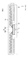
- FIG. 1 is a laminated cross-sectional view of the RFID tag 100 according to the embodiment.
- the RFID tag 100 is a substantially flat device attached to the object to be attached 200.
- the RFID tag includes an inlay 101, a magnetic sheet 102, and a spacer layer 103.
- the object to be attached 200 is, for example, a metal.
- the metal includes metals such as iron, aluminum, and copper, as well as alloys of metals such as iron alloys, aluminum alloys, and copper alloys.
- the inlay 101 is a part including elements related to the function of the RFID tag 100, and is an IC chip 10 on which identification information is recorded, a loop-shaped conductor 20 connected to the IC chip 10, and an antenna connected to the loop-shaped conductor 20. It has a portion 30 (see FIG. 2).
- an antenna portion 30 in which an aluminum sheet is attached by dry lamination is formed on a PET film, and an IC chip 10 is mounted at a specified position.
- the magnetic sheet 102 is a sheet material containing a magnetic material, and is laminated on the side of the inlay 101 to be attached to the object 200.
- the magnetic sheet 102 is formed by kneading a magnetic powder such as a stainless steel alloy into a rubber material, a resin, or the like so as to be uniformly oriented and dispersed.
- the spacer layer 103 is an element for arranging the inlay 101 and the magnetic sheet 102 in a state of being separated from the object to be attached 200 by the thickness thereof.
- the spacer layer 103 is laminated on the side of the magnetic sheet 102 to be attached to the object 200, and is arranged between the magnetic sheet 102 and the object to be attached 200.
- the spacer layer 103 is preferably formed of, for example, an insulator such as a woven fabric made of fibers such as cardboard or synthetic resin, a non-woven fabric, or a sheet of an inorganic material such as ceramic glass.
- the spacer layer 103 is formed of a material that can be arbitrarily deformed together with the inlay 101 and the magnetic sheet 102 in response to an external force, whereby the RFID tag 100 can be easily attached even when the attachment surface of the attachment object 200 is curved. It is preferably configured so that it can be attached and the versatility can be improved, and thick paper is preferable.
- the thickness of the spacer layer 103 is preferably about 300 ⁇ m to 2 mm. If the thickness is smaller than 300 ⁇ m, the communicable distance of the RFID tag 100 becomes too short and the communication performance deteriorates. If the thickness is larger than 2 mm, the RFID tag 100 protrudes too much with respect to the object to be attached 200, which is not easy to use. This is to become.
- the spacer layer 103 may have a structure in which at least the inlay 101 and the magnetic sheet 102 can be separated from the object to be attached 200 by a predetermined distance, and may have a configuration other than the sheet-shaped member as shown in FIG. For example, a plurality of legs extending from the magnetic sheet 102 toward the object to be attached 200 may be provided, and an air layer may be provided between the magnetic sheet 102 and the object to be attached 200.
- the RFID tag 100 includes an IC chip 10 on which identification information is recorded, a loop-shaped conductor 20 connected to the IC chip 10, and an antenna portion 30 connected to the loop-shaped conductor 20.
- the inlay 101 is provided with a magnetic sheet 102 laminated on the side of the inlay 101 to be attached to the object 200, and a spacer layer 103 arranged between the magnetic sheet 102 and the object to be attached 200.
- the magnetic sheet 102 and the spacer layer 103 are interposed between the inlay 101 having a communication function and the object to be attached 200. Therefore, the magnetic sheet 102 circulates the electromagnetic waves received by the antenna inside the magnetic sheet 102. , The energy supplied to the IC chip 10 of the inlay 101 can be efficiently transmitted. Further, the spacer layer 103 allows the inlay 101 to be arranged away from the object to be attached 200, and the influence of the object to be attached 200 on communication can be suppressed. As a result, the communication performance of the RFID tag 100 can be improved.
- the RFID tag 100 of the present embodiment can suppress the influence of the sticking object 200 on the communication by providing the spacer layer 103 as described above, so that the RFID tag 100 can communicate regardless of the type of the sticking object 200. .. Then, when the object to be attached 200 is made of metal, the effect of improving the communication performance becomes particularly remarkable.
- FIG. 2 is a plan view of the RFID tag 100 in FIG. 1, and is a diagram showing an example of a pattern of the antenna portion 30 from above the inlay 101.
- the inlay 101 of the RFID tag 100 includes a strip-shaped sheet 40, an IC chip 10, a loop-shaped conductor 20, and an antenna portion 30.
- the sheet 40 is a film formed in a strip shape by laminating a plurality of synthetic resin films such as polyethylene terephthalate and polypropylene.
- the IC chip 10, the loop-shaped conductor 20, and the antenna portion 30 are arranged so as to be sandwiched between, for example, a plurality of synthetic resin films to be laminated.
- the IC chip 10 has an internal capacitance, and a matching circuit is formed by the inductance of the antenna unit 30 and the internal capacitance of the IC chip 10.
- the loop-shaped conductor 20 is a loop-shaped (annular) conductive wiring pattern in which the sheet 40 is viewed in a plan view in the Z-axis direction for one turn or less.
- the loop-shaped conductor 20 is electrically connected to the IC chip 10 and the antenna portion 30.
- the identification information recorded on the IC chip 10 is read by a reader
- the antenna unit 30 receives a radio wave in the UHF band, for example, a radio wave in the vicinity of 920 MHz
- a current flows through the loop-shaped conductor 20 due to resonance action.
- an electromotive force for operating the IC chip 10 is generated.
- the identification information recorded on the IC chip 10 is encoded by the IC chip 10, and the encoded data is wirelessly transmitted to a communication device such as a reader using a radio wave near 920 MHz as a carrier wave.
- a communication device such as a reader using a radio wave near 920 MHz as a carrier wave.
- the RFID tag 100 of this embodiment is a passive radio wave type wireless tag that does not have a power source (battery) for holding and transmitting identification information. Therefore, as compared with the active wireless tag having a battery, the size and price can be reduced because the tag does not have a battery.
- the antenna unit 30 is a dipole antenna configured to exhibit resonance characteristics with the IC chip 10 with respect to the frequency of radio communication radio waves (for example, the frequency in the UHF band).
- the antenna portion 30 has an electric length corresponding to the vicinity of ⁇ / 2 ( ⁇ is a communication wavelength) as a whole.
- the antenna unit 30 has a structure that realizes impedance conjugate matching with the IC chip 10 for radio waves having a frequency of, for example, around 920 MHz (for example, 860 MHz to 960 MHz, more preferably 915 MHz to 935 MHz).
- the antenna portion 30 includes two conductor portions (conductor portion 30A and conductor portion 30B) as a structure for realizing impedance conjugate matching with the IC chip 10.
- the conductor portion 30A and the conductor portion 30B are conductive wiring patterns that are connected to the loop-shaped conductor 20 and extend in a direction away from each other from the loop-shaped conductor 20. Conductive wiring patterns can be formed by existing methods such as press working and etching of copper foil and aluminum foil, forming by plating, silk screen printing of metal paste, metal wire, etc., but here by etching aluminum Formed.
- the conductor portion 30A and the conductor portion 30B are formed line-symmetrically with respect to the virtual line VL passing through the substantially center of the IC chip 10.
- the virtual line VL is a line parallel to the XY plane and extending in the Y-axis direction.
- the virtual line VL is also a line that substantially bisects the RFID tag 100 in the region in the X-axis direction.
- Each of the conductor portion 30A and the conductor portion 30B has an electric length corresponding to the vicinity of ⁇ / 4 ( ⁇ is a communication wavelength).
- ⁇ is a communication wavelength.
- the configuration of the conductor portion 30A will be described below.
- the configuration of the conductor portion 30B the description thereof will be omitted by reading the extending direction of the conductor portion 30A in the X-axis direction in reverse.
- the conductor portion 30A includes a first element 1, a second element 2, a third element 3, and a fourth element 4.
- the first element 1 is a meander-shaped conductive wiring pattern extending from the loop-shaped conductor 20 in the minus X-axis direction.
- the first element 1 is a meander element.
- the end of the first element 1 in the plus X-axis direction is connected to the loop-shaped conductor 20.
- the connection point between the first element 1 and the loop-shaped conductor 20 is, for example, a peripheral edge portion of the loop-shaped conductor 20 on the plus Y-axis direction side.
- the first element 1 is extended by a predetermined distance (for example, 30 ° to 60 °) with respect to the minus X-axis direction from the connection point with the loop conductor 20, and is extended in the minus X-axis direction from the point where the first element 1 is extended by a certain distance. Further stretch.
- the shape of the first element 1 is not limited to the illustrated example.
- the shape of the first element 1 is extended by a certain distance in the plus Y-axis direction from the connection point with the loop-shaped conductor 20, and is bent vertically from the point where the first element 1 is extended by a certain distance to be minus X. It may have a shape that extends in the axial direction.
- the width of the entire antenna portion 30 in the X-axis direction is narrowed, and the RFID tag has a small ratio of vertical width to horizontal width. 100 can be realized. Therefore, for example, even when the RFID tag 100 is attached to a small-capacity PET bottle having a relatively small height in the X-axis direction and a small label, the RFID is located in an area that does not interfere with the display of the product or the like on the PET bottle label. The tag 100 can be placed.
- the connection point between the first element 1 and the loop-shaped conductor 20 is not limited to this, and may be the peripheral edge portion of the loop-shaped conductor 20 in the minus X-axis direction.
- the first element 1 can be arranged in the region of the loop-shaped conductor 20 on the minus X-axis direction side. Therefore, the width of the entire antenna portion 30 in the Y-axis direction is narrowed, and the RFID tag 100 having an elongated shape can be realized. Therefore, for example, even when the RFID tag 100 is attached to a large-capacity PET bottle having a relatively large height in the X-axis direction, the RFID tag 100 can be arranged in an area that does not interfere with the display of products or the like on the PET bottle.
- the second element 2 is, for example, a linear conductive wiring pattern extending from the loop-shaped conductor 20 in the minus X-axis direction.
- the second element 2 is a linear element.
- the end of the second element 2 in the plus X-axis direction is connected to the first element 1 or the loop-shaped conductor 20.
- the second element 2 When the second element 2 is connected to the first element 1, the second element 2 is connected, for example, in the vicinity of the connection point between the first element 1 and the loop-shaped conductor 20.
- the second element 2 extends a certain distance from the connection point in the minus X-axis direction.
- the second element 2 When the second element 2 is connected to the loop-shaped conductor 20, the second element 2 is connected to, for example, the peripheral edge portion of the loop-shaped conductor 20 on the plus Y-axis direction side.
- the second element 2 may be provided on the minus Y-axis direction side of the first element 1 or may be provided on the plus Y-axis direction side of the first element 1.
- the region of the loop-shaped conductor 20 on the minus X-axis direction side can be effectively used. Therefore, it is possible to realize the RFID tag 100 having a small ratio of vertical width to horizontal width.
- the gap (separation distance in the Y-axis direction) between the second element 2 and the first element 1 is set to a value of, for example, 0.5 mm to 2.0 mm, the impedance of the antenna and the IC chip It is preferable because it makes it easy to take a complex conjugate. If this distance becomes too large, the real part of the impedance becomes large, and it becomes difficult to obtain a complex conjugate with the IC chip.
- the second element 2 is the main part
- the first element 1 is the sub part.
- the third element 3 is a hook-shaped conductive wiring pattern that extends from the tip of the second element 2 in the minus X-axis direction in a direction different from the direction in which the second element 2 extends.
- the third element 3 is a hook element.
- the third element 3 may be a U-shaped pattern or an L-shaped pattern.
- the second element 2 and the third element 3 may be integrally formed in a hook shape.
- the third element 3 extends from the tip of the second element 2 in the minus X-axis direction by a certain distance in the minus Y-axis direction, and then bends perpendicularly in the plus X-axis direction to form a loop-shaped conductor 20. Stretch a certain distance toward. Due to this shape, the region of the loop-shaped conductor 20 on the minus X-axis direction side can be effectively used. Therefore, it is possible to realize the RFID tag 100 having a small ratio of vertical width to horizontal width.
- a gap is formed between the portion where the third element 3 extends toward the loop-shaped conductor 20 and the second element.
- This gap (separation distance in the Y-axis direction) is set to a value from 1.0 mm to 30.0 mm, for example.
- a plurality of fourth elements 4 are provided in this gap.
- the fourth element 4 is a conductive wiring pattern that extends from the second element 2 toward the third element 3 and forms a lattice-shaped pattern together with the second element 2 and the third element 3.
- the fourth element 4 is a lattice element.
- five fourth elements 4 are used as an example, but the number of the fourth elements 4 may be one or more.
- the distance between the adjacent fourth elements 4 in the X-axis direction is set to a value of, for example, 1.0 mm to 30.0 mm, it is preferable in that the communicable frequency band is widened and the communication distance is extended.
- the electrical length of each element is set as follows.
- the length of the first element 1 is set to an electric length that is a multiple of ⁇ / 4 of the wavelength of the operating frequency.
- at least one of the length of the second element 2 and the length of the third element 3 is set to an electric length different from the electric length which is a multiple of ⁇ / 4.
- the different electrical lengths range, for example, from ⁇ / 3.5 to ⁇ / 4.5 of the wavelength of use frequency.
- the electric length of the second element 2 may be set to a multiple of ⁇ / 4 of the wavelength of the operating frequency.
- at least one of the electric length of the first element 1 and the electric length of the third element 3 is set to an electric length different from the electric length which is a multiple of ⁇ / 4 of the wavelength of the working frequency.
- the different electrical lengths in this case are, for example, in the range of ⁇ / 3.5 to ⁇ / 4.5 of the wavelength of the working frequency.
- the sum of the electric length of the second element 2 and the electric length of the third element 3 having an L-shape (inverted L-shape) is ⁇ / 4 of the wavelength of the operating frequency. It may be set to a multiple of.
- the electric length of the first element 1 is set to a different electric length from the electric length which is a multiple of ⁇ / 4 of the wavelength of the working frequency.
- the different electrical lengths in this case are, for example, in the range of ⁇ / 3.5 to ⁇ / 4.5 of the wavelength of the working frequency.
- the electric length of the second element 2 may be set to a multiple of ⁇ / 4 of the wavelength of the frequency used.
- the electric length of the first element 1 is set to a different electric length from the electric length which is a multiple of ⁇ / 4 of the wavelength of the working frequency.
- the different electrical lengths in this case are, for example, in the range of ⁇ / 3.5 to ⁇ / 4.5 of the wavelength of the working frequency.
- the RFID tag 100 it is possible to increase the reception intensity of radio waves in the antenna unit 30 by combining a plurality of antenna elements having different shapes or by combining a plurality of elements having different electric lengths. it can.
- the RFID tag 100 may be configured as follows. The same parts as the RFID tag 100 are designated by the same reference numerals, the description thereof will be omitted, and different parts will be described.
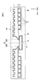
- FIG. 3 is a diagram showing a configuration example of the RFID tag 100-1 according to the first modification.
- the RFID tag 100-1 is configured so that the distance from the first element 1 to the second element 2 in the Y-axis direction is wide.
- the gap between the first element 1 and the second element 2 is set to a value of, for example, 2.0 mm to 5.0 mm, it is easy to obtain the complex conjugate of the antenna and the IC chip. It is preferable in that. If the gap between the first element 1 and the second element 2 is 5.0 mm or more, the resistance of the antenna becomes high and the communication distance may decrease.
- the same effect as that of the RFID tag 100 can be obtained. Further, according to the RFID tag 100-1, for example, even if the vertical width of the first element 1 having a meander shape is not uniform due to manufacturing tolerances, the gap between the first element 1 and the second element 2 is widened, so that the first element 1 The contact of the element 1 with the second element 2 can be suppressed. Therefore, it is not necessary to manage the manufacturing tolerance of the first element 1 and the like. Further, the widening of the gap between the first element 1 and the second element 2 facilitates the manufacture of each wiring pattern. As a result, the yield of the RFID tag 100-1 can be improved and the manufacturing cost can be reduced.
- FIG. 4 is a diagram showing a configuration example of the RFID tag 100-2 according to the second modification.
- the RFID tag 100-2 omits the first element 1 as compared with the RFID tag 100.
- the electrical length of each element is set as follows.
- the length of the second element 2 is set to an electric length that is a multiple of ⁇ / 4 of the wavelength of the frequency used.
- the length of the third element 3 is set to an electric length different from the electric length which is a multiple of ⁇ / 4.
- the different electrical lengths range, for example, from ⁇ / 3.5 to ⁇ / 4.5 of the wavelength of use frequency.
- the electric length of the third element 3 may be set to a multiple of ⁇ / 4 of the wavelength of the operating frequency.
- the length of the second element 2 is set to an electric length different from the electric length which is a multiple of ⁇ / 4.
- the different electrical lengths range, for example, from ⁇ / 3.5 to ⁇ / 4.5 of the wavelength of use frequency.
- the total electric length of the third element 3 and the fourth element 4 (for example, any one of the three fourth elements 4) is calculated as the total electric length. It may be set to a multiple of ⁇ / 4 of the wavelength of the operating frequency.
- the electric length of the second element 2 is set to a different electric length from the electric length which is a multiple of ⁇ / 4 of the wavelength of the working frequency.
- the different electrical lengths in this case are, for example, in the range of ⁇ / 3.5 to ⁇ / 4.5 of the wavelength of the working frequency.
- the same effect as the RFID tag 100 can be obtained by combining a plurality of elements having different electric lengths and shapes.
- the RFID tag 100-2 for example, since the first element 1 is unnecessary, not only the management of the manufacturing tolerance of the first element 1 or the like becomes unnecessary, but also the structure is simplified. As a result, the yield of the RFID tag 100-2 can be improved, and the manufacturing cost can be further reduced.
- FIG. 5 is a diagram showing a configuration example of the RFID tag 100-3 according to the third modification.
- the RFID tag 100-3 has a smaller number of fourth elements 4 than the RFID tag 100-2.
- the same effect as the RFID tag 100 can be obtained by combining a plurality of elements having different electric lengths and shapes.
- the number of the fourth element 4 can be reduced, not only the management of the manufacturing tolerance becomes unnecessary, but also the structure is simplified. As a result, the yield of the RFID tag 100-3 can be improved, and the manufacturing cost can be further reduced.
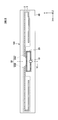
- FIG. 6 is a diagram showing a configuration example of the RFID tag 100-4 according to the fourth modification. Compared to RFID tag 100-3, RFID tag 100-4 uses a fifth element 5 instead of the third element 3 and the fourth element 4.
- the second element 2 is the main part, and the fifth element 5 is the sub part.
- the fifth element 5 is a conductor that is connected to the second element 2 so as to branch off from the middle of the second element 2, which is a linear element, and extends in parallel with the second element 2.
- the fifth element 5 is a branch element.
- connection point of the fifth element 5 to the second element 2 is, for example, a position separated from the connection point of the second element 2 and the loop-shaped conductor 20 by a predetermined distance.
- the predetermined distance is set to a value from, for example, 5.0 mm to 100.0 mm, the resistance of the antenna does not become too high, which is preferable.
- a gap is formed between the second element 2 and the portion where the fifth element 5 extends in the direction opposite to the loop-shaped conductor 20 side.
- this gap separation distance in the Y-axis direction
- the resistance of the antenna does not become too high, which is preferable.
- the above-mentioned fourth element 4 may be provided in this gap.
- the electrical length of each element is set as follows.
- the length of the second element 2 is set to an electric length that is a multiple of ⁇ / 4 of the wavelength of the frequency used.
- the length of the fifth element 5 is set to an electric length different from the electric length which is a multiple of ⁇ / 4.
- the different electrical lengths range, for example, from ⁇ / 3.5 to ⁇ / 4.5 of the wavelength of use frequency.
- the electric length of the fifth element 5 may be set to a multiple of ⁇ / 4 of the wavelength of the operating frequency.
- the electric length of the second element 2 is set to a different electric length from the electric length which is a multiple of ⁇ / 4 of the wavelength of the working frequency.
- the different electrical lengths in this case are, for example, in the range of ⁇ / 3.5 to ⁇ / 4.5 of the wavelength of the working frequency.
- the same effect as the RFID tag 100 can be obtained by combining a plurality of elements having different electric lengths and shapes.
- the fourth element 4 can be omitted, not only the management of the manufacturing tolerance becomes unnecessary, but also the structure is simplified. As a result, the yield of the RFID tag 100-4 can be improved, and the manufacturing cost can be further reduced.
- the design condition of the RFID tag 100-4 is such that the branching point of the fifth element 5, that is, the pull-out position of the fifth element 5 from the second element 2 can be easily adjusted. Can be given a degree of freedom.
- the object to be attached 200 is a container having a special shape in which the surface area of the RFID tag 100-4 must be made as small as possible, the area on the lower side (minus Y-axis direction side) of the second element 2 may be narrowed. is assumed. Even in this case, it can be applied to a special container by making the branching point of the fifth element 5 as close as possible to the loop-shaped conductor 20 and shortening the length of the portion extending in the X-axis direction of the fifth element 5. It becomes. Therefore, as the number of containers to which the RFID tag 100-4 can be applied increases, the production amount of the RFID tag 100-4 can be increased, and the manufacturing unit price of the RFID tag 100-4 can be further reduced.
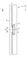
- FIG. 7 is a diagram showing a configuration example of the RFID tag 100-5 according to the fifth modification.
- the RFID tag 100-5 omits the fifth element 5 as compared with the RFID tag 100-4.
- the RFID tag 100-5 has a simple structure including a second element 2 instead of a structure in which a plurality of elements having different electric lengths and shapes are combined.
- the second element 2 of the RFID tag 100-5 is a linear conductor set to an electric length that is a multiple of approximately 1/4 of the wavelength of the frequency used.
- the communication distance with the reader by the RFID tag 100-5 tends to be shorter than the communication distance with the reader by the RFID tags 100 to 100-4, but at least the practical communication distance (for example, about 1 m to 7 m) is set. It was confirmed by the inventor of the present application that it can be secured. Even when the communication distance is shortened, the identification information can be read by arranging the reader on the belt conveyor that conveys the container, for example, so that it can be used for inventory management of all products.
- the reason why the impedance characteristics of the RFID tag 100-5 are excellent is that by making the antenna element linear, the electrical coupling between the antenna element and the liquid is better than when only the antenna element of the meander shape is used. It is thought that it is weakened.
- a meander-shaped antenna element, a loop-shaped antenna element, or the like is often adopted.
- the electrical coupling with the liquid becomes strong and the impedance characteristics are greatly disturbed, so that the desired antenna performance cannot be ensured. Therefore, conventionally, a spacer is provided between the antenna element and the container to reduce the electrical coupling by separating the distance from the antenna element to the liquid, and a metal sheet is inserted between the antenna element and the container to electrically reduce the electrical coupling. Measures such as reducing the bond were taken.
- the RFID tag 100-5 According to the RFID tag 100-5 according to the fifth modification, such measures are not required, so that the management of the production of the RFID tag 100-5 is facilitated and the RFID tag 100-5 is required to be manufactured.
- the material can be significantly reduced. Therefore, it is possible to realize a significant reduction in the manufacturing cost of the RFID tag 100-5.
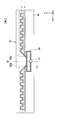
- FIG. 8 is a diagram showing a configuration example of the RFID tag 100-6 according to the sixth modification.
- the RFID tag 100-6 omits the fourth element 4 as compared with the RFID tag 100-3 according to the third modification.
- the communication distance with the reader by the RFID tag 100-6 is equivalent to the communication distance with the reader by the RFID tag 100-3.
- the fourth element 4 can be omitted, not only the management of manufacturing tolerances becomes unnecessary, but also the structure is simplified. As a result, the yield of the RFID tag 100-6 can be improved, and the manufacturing cost can be further reduced.
- FIG. 9 is a diagram showing a configuration example of the RFID tag 100-7 according to the seventh modification.
- the RFID tag 100-7 omits the third element 3 and the fourth element 4 as compared with the RFID tag 100.
- the first element 1 is the main part
- the second element 2 is the sub part
- the first element 1 is the sub part.
- the electrical length of each element is set as follows.
- the length of the first element 1 is set to an electric length that is a multiple of ⁇ / 4 of the wavelength of the operating frequency.
- the length of the second element 2 is set to an electric length different from the electric length which is a multiple of ⁇ / 4.
- the different electrical lengths range, for example, from ⁇ / 3.5 to ⁇ / 4.5 of the wavelength of use frequency.
- the electric length of the second element 2 may be set to a multiple of ⁇ / 4 of the wavelength of the operating frequency.
- the electric length of the first element 1 is set to a different electric length from the electric length which is a multiple of ⁇ / 4 of the wavelength of the working frequency.
- the different electrical lengths in this case are, for example, in the range of ⁇ / 3.5 to ⁇ / 4.5 of the wavelength of the working frequency.
- the third element 3 and the fourth element 4 can be omitted, not only the management of manufacturing tolerances becomes unnecessary, but also the structure is simplified. As a result, the yield of the RFID tag 100-7 can be improved, and the manufacturing cost can be further reduced.
- FIG. 10 is a diagram showing a configuration example of the RFID tag 100-8 according to the eighth modification.
- the fifth element 5 is used instead of the third element 3 and the fourth element 4 as compared with the RFID tag 100.
- the first element 1 is the main part
- the second element 2 is the sub part
- the first element 1 is the sub part.
- the electrical length of each element is set as follows.
- the length of the first element 1 is set to an electrical length that is a multiple of ⁇ / 4 of the wavelength of the working frequency
- at least one of the length of the second element 2 and the length of the fifth element 5 becomes.
- the electrical length is set to be different from the electrical length that is a multiple of ⁇ / 4.
- the different electrical lengths range, for example, from ⁇ / 3.5 to ⁇ / 4.5 of the wavelength of use frequency.
- the length of the second element 2 is set to an electric length that is a multiple of ⁇ / 4 of the wavelength of the working frequency
- at least one of the length of the first element 1 and the length of the fifth element 5 becomes.
- the electrical length is set to be different from the electrical length that is a multiple of ⁇ / 4.
- the different electrical lengths range, for example, from ⁇ / 3.5 to ⁇ / 4.5 of the wavelength of use frequency.
- the electric length of the fifth element 5 is set to a multiple of ⁇ / 4 of the wavelength of the operating frequency
- at least one of the electric length of the first element 1 and the length of the second element 2 is ⁇ /.
- the electric length is set to be different from the electric length that is a multiple of 4.
- the different electrical lengths range, for example, from ⁇ / 3.5 to ⁇ / 4.5 of the wavelength of use frequency.
- the fourth element 4 can be omitted, not only the management of the manufacturing tolerance becomes unnecessary, but also the structure is simplified. As a result, the yield of the RFID tag 100-8 can be improved, and the manufacturing cost can be further reduced.
- FIG. 11 is a diagram showing a configuration example of the RFID tag 100-9 according to the ninth modification. The difference from the RFID tag 100-2 shown in FIG. 4 is that the number of the fourth element 4 is increased in the RFID tag 100-9.
- the reception strength of radio waves in the antenna unit 30 can be increased by combining a plurality of elements having different electric lengths.
- the number of the fourth elements 4 it is possible to further increase the reception intensity of radio waves in the antenna unit 30 even in underwater applications.
- each of the RFID tags 100 to 100-9 can be applied not only to radio waves in the UHF band but also to radio waves in the VHF band, SHF band, and the like.
- the frequency used by the RFID tags 100 to 100-9 is the frequency of the UHF band, for example, 860 to 960 MHz, 915 to 925 MHz, etc.
- the frequency of the UHF band is higher than that of the VHF band, so that the frequency is shorter and the antenna has a shorter frequency. It is advantageous for miniaturization. Therefore, by shaping the RFID tags 100 to 100-9 into a shape suitable for radio waves in the UHF band, it is possible to reduce the size of the IC chip 10 and obtain an inexpensive wireless tag with a small memory capacity.
- each of the RFID tags 100 to 100-9 can be applied to either an electromagnetic induction type wireless tag or a radio wave type wireless tag.
- a predetermined wireless communication distance with the reader can be secured.
- the predetermined wireless communication distance is, for example, in the range of 0 m to 20 m.
- the RFID tags 100 to 100-9 include the UHF band and the VHF band regardless of whether the RFID tags 100 to 100-9 are present in the air (air) or in water.
- Wireless communication is possible using radio waves such as the SHF band.
- the RDID tag 100 may be formed by laminating at least the inlay 101, the magnetic sheet 102, and the spacer layer 103 in this order, and the antenna pattern of the antenna portion 30 is the RFID tag 100 described above.
- the shape may be different from that of ⁇ 100-9.
- Example 1 The RFID tag 100 shown in FIG. 1 was created by laminating an inlay 101, a magnetic sheet 102 having a thickness of 80 ⁇ m, and a spacer layer 103 made of thick paper having a thickness of 550 ⁇ m.
- an antenna portion 30 in which a 10 ⁇ m aluminum sheet was attached by dry lamination was formed on a PET film having a thickness of 38 ⁇ m, and the IC chip 10 was mounted at a specified position.
- the antenna pattern of the antenna portion 30 has the shape shown in FIG.
- the frequency characteristics of the RFID tag 100 were measured using an RFID tag performance inspection device (Tagformance Pro, manufactured by Voyanti).
- the measurement frequency band of the radio wave for wireless communication at the time of measurement was 700 to 1200 MHz, and the EIRP (Equivalent Isotropically Radiated Power) was 3.28 W.
- Example 2 The RFID tag 100 was prepared and the frequency characteristics were measured in the same manner as in Example 1 except that the thickness of the magnetic sheet 102 was 120 ⁇ m.
- Example 3 The RFID tag 100 was prepared and the frequency characteristics were measured in the same manner as in Example 1 except that the thickness of the magnetic sheet 102 was set to 200 ⁇ m.
- Example 1 The RFID tag 100 was created in the same manner as in Example 1 except that the spacer layer 103 was excluded. That is, an RFID tag was created by laminating an inlay 101 and a magnetic sheet 102 having a thickness of 80 ⁇ m. Further, the frequency characteristics of the created RFID tag were measured by the same method as in Example 1.
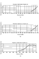
- FIG. 12 is a diagram showing the frequency characteristics of the RFID tags of Comparative Examples 1 to 3.
- (a) shows the frequency characteristics of Comparative Example 1
- (b) shows the frequency characteristics of Comparative Example 2
- (c) shows the frequency characteristics of Comparative Example 3.
- the horizontal axis of each figure represents the frequency of radio waves for wireless communication
- the vertical axis represents the communicable distance from the RFID tag 100 to the reader.
- the characteristic graph is not shown in FIG. 12, it is shown that wireless communication could not be performed between the RFID tag 100 and the reader.
- Comparative Example 3 where the magnetic sheet 102 is the thickest, wireless communication could not be performed in the frequency band of about 920 MHz or less, and in Comparative Example 2 and the thinnest Comparative Example 3 where the magnetic sheet 102 was the thickest, wireless communication could not be performed in the frequency band of about 1020 MHz or less. As described above, in Comparative Examples 1 to 3, when the magnetic sheet 102 was thin, communication could not be performed in the UHF band.
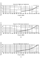
- FIG. 13 is a diagram showing the frequency characteristics of the RFID tags 100 of Examples 1 to 3.
- (a) shows the frequency characteristics of Example 1
- (b) shows the frequency characteristics of Example 2
- (c) shows the frequency characteristics of Example 3.
- the horizontal axis and the vertical axis of each figure are the same as those in FIG.
- the communicable frequency band extends to the lower frequency side than in Comparative Examples 1 to 3, and the UHF band is sufficient for communication regardless of the thickness of the magnetic sheet 102. It is a possible characteristic.
- Example 4 The RFID tag 100 was prepared and the frequency characteristics were measured in the same manner as in Example 1 except that the thickness of the spacer layer 103 was doubled to 1100 ⁇ m.
- Example 5 The RFID tag 100 was prepared and the frequency characteristics were measured in the same manner as in Example 2 except that the thickness of the spacer layer 103 was doubled to 1100 ⁇ m.
- Example 6 The RFID tag 100 was prepared and the frequency characteristics were measured in the same manner as in Example 3 except that the thickness of the spacer layer 103 was doubled to 1100 ⁇ m.
- Example 7 The RFID tag 100 was created and the frequency characteristics were measured in the same manner as in Example 1 except that the thickness of the spacer layer 103 was tripled to 1650 ⁇ m.
- Example 8 The RFID tag 100 was prepared and the frequency characteristics were measured in the same manner as in Example 2 except that the thickness of the spacer layer 103 was tripled to 1650 ⁇ m.
- Example 9 The RFID tag 100 was prepared and the frequency characteristics were measured in the same manner as in Example 3 except that the thickness of the spacer layer 103 was tripled to 1650 ⁇ m.
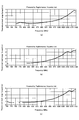
- FIG. 14 is a diagram showing the frequency characteristics of the RFID tags 100 of Examples 4 to 6.
- (a) shows the frequency characteristics of Example 4
- (b) shows the frequency characteristics of Example 5
- (c) shows the frequency characteristics of Example 6.
- the horizontal axis and the vertical axis of each figure are the same as those in FIG.
- the communicable frequency band extends to the lower frequency side than in Examples 1 to 3, and the UHF band is sufficient for communication regardless of the thickness of the magnetic sheet 102. It is a possible characteristic.
- FIG. 15 is a diagram showing the frequency characteristics of the RFID tags 100 of Examples 7 to 9.
- (a) shows the frequency characteristics of Example 7
- (b) shows the frequency characteristics of Example 8
- (c) shows the frequency characteristics of Example 9.
- the horizontal axis and the vertical axis of each figure are the same as those in FIG.
- the communicable frequency band is further extended to the low frequency side as compared with Examples 4 to 6, and the UHF band is sufficient regardless of the thickness of the magnetic sheet 102. It has the characteristics of being able to communicate.
Landscapes
- Engineering & Computer Science (AREA)
- Microelectronics & Electronic Packaging (AREA)
- Physics & Mathematics (AREA)
- Computer Hardware Design (AREA)
- General Physics & Mathematics (AREA)
- Theoretical Computer Science (AREA)
- Computer Networks & Wireless Communication (AREA)
- Electromagnetism (AREA)
- Details Of Aerials (AREA)
Abstract
An RFID tag provided with: an inlay having an IC chip in which identification information is recorded, a looped conductor connected to the IC chip, and an antenna unit connected to the looped conductor; a magnetic sheet laminated on the side of the inlay to which side an object is to be pasted; and a spacer layer arranged between the magnetic sheet and the object to be pasted.
Description
本開示は、RFIDタグに関する。
This disclosure relates to RFID tags.
物流管理や商品管理のため、貼付対象物に貼付されるRFID(Radio Frequency Identification)タグが普及している。RFIDタグは、ICチップとICチップに電気的に接続されるアンテナとを備える。RFIDタグは、無線タグ、ICタグ、RF-IDタグ、RFタグと呼ばれることもある。
RFID (Radio Frequency Identification) tags that are affixed to objects to be affixed are widespread for distribution management and product management. RFID tags include an IC chip and an antenna that is electrically connected to the IC chip. RFID tags are sometimes called wireless tags, IC tags, RF-ID tags, and RF tags.
このようなRFIDタグが貼付される貼付対象物が金属製である場合、タグ内のアンテナによる通信ができず、識別情報の読み出しに支障をきたすことがある。これは、金属がRFIDタグの周辺にあると、データを送受信するリーダライタからRFIDタグに送られた電磁波が、金属部で過電流として損失してしまうため、ICチップからデータを再びアンテナに打ち返すためのエネルギが効率的に得られないことが原因と推測される。
If the object to be attached to which such an RFID tag is attached is made of metal, communication by the antenna inside the tag may not be possible, which may hinder the reading of identification information. This is because if the metal is around the RFID tag, the electromagnetic waves sent from the reader / writer that sends and receives data to the RFID tag will be lost as an overcurrent at the metal part, so the data will be returned to the antenna from the IC chip again. It is presumed that the cause is that the energy for this is not efficiently obtained.
これらの問題を解決する手段として、磁性シートの使用が有効であることが知られている。RFIDタグと、貼付対象物である金属との間に磁性シートを挟むことで、アンテナが受けた電磁波を磁性シート内部で循環させ、ICチップに供給するエネルギを効率的に伝送することができる(例えば非特許文献1参照)。
It is known that the use of a magnetic sheet is effective as a means for solving these problems. By sandwiching the magnetic sheet between the RFID tag and the metal to be attached, the electromagnetic waves received by the antenna can be circulated inside the magnetic sheet, and the energy supplied to the IC chip can be efficiently transmitted (). For example, see Non-Patent Document 1).
ところで、RFIDタグの通信に用いられる周波数帯は、HF帯(13.56MHz、電磁誘導方式)と比較して長距離通信や複数の対象物の一括読み取りが可能となるUHF帯(電波方式)のニーズが高まっている。しかしながら、従来のRFIDタグと金属との間に磁性シートを挟む構成では、磁性シートが薄い場合にはUHF帯で通信ができない虞がある。
By the way, the frequency band used for RFID tag communication is the UHF band (radio wave method), which enables long-distance communication and batch reading of a plurality of objects as compared with the HF band (13.56 MHz, electromagnetic induction method). Needs are increasing. However, in the conventional configuration in which the magnetic sheet is sandwiched between the RFID tag and the metal, if the magnetic sheet is thin, communication may not be possible in the UHF band.
本開示は、通信性能を向上できるRFIDタグを提供することを目的とする。
The object of the present disclosure is to provide an RFID tag capable of improving communication performance.
上述した課題を解決するために、本発明の一観点に係るRFIDタグは、貼付対象物に添付されるRFIDタグであって、識別情報が記録されるICチップと、前記ICチップに接続されるループ状導体と、前記ループ状導体に接続されるアンテナ部と、を有するインレイと、前記インレイの前記貼付対象物側に積層される磁性シートと、前記磁性シートと前記貼付対象物との間に配置されるスペーサ層と、を備える。
In order to solve the above-mentioned problems, the RFID tag according to one aspect of the present invention is an RFID tag attached to an object to be attached, and is connected to an IC chip on which identification information is recorded and the IC chip. An inlay having a loop-shaped conductor and an antenna portion connected to the loop-shaped conductor, a magnetic sheet laminated on the side of the inlay to be attached, and between the magnetic sheet and the object to be attached. It comprises a spacer layer to be arranged.
本開示によれば、通信性能を向上できるRFIDタグを提供することができる。
According to the present disclosure, it is possible to provide an RFID tag capable of improving communication performance.
以下、添付図面を参照しながら実施形態について説明する。説明の理解を容易にするため、各図面において同一の構成要素に対しては可能な限り同一の符号を付して、重複する説明は省略する。
Hereinafter, embodiments will be described with reference to the attached drawings. In order to facilitate understanding of the description, the same components are designated by the same reference numerals as much as possible in each drawing, and duplicate description is omitted.
なお、以下の説明において、X方向、Y方向、Z方向は互いに垂直な方向である。X方向は、後述するアンテナ部30の第1エレメント1や第2エレメント2の延在方向である。Y方向は、後述するアンテナ部30の第1エレメント1や第2エレメント2の配列方向である。Z方向は、RFIDタグ100のインレイ101、磁性シート102の積層方向である。また、以下では説明の便宜上、Z正方向側を上側、Z負方向側を下側とも表現する場合がある。
In the following description, the X direction, the Y direction, and the Z direction are perpendicular to each other. The X direction is the extending direction of the first element 1 and the second element 2 of the antenna portion 30, which will be described later. The Y direction is the arrangement direction of the first element 1 and the second element 2 of the antenna unit 30, which will be described later. The Z direction is the stacking direction of the inlay 101 of the RFID tag 100 and the magnetic sheet 102. Further, in the following, for convenience of explanation, the Z positive direction side may be expressed as the upper side and the Z negative direction side may be expressed as the lower side.
図1は、実施形態に係るRFIDタグ100の積層断面図である。RFIDタグ100は、貼付対象物200に貼付される略平面状の装置である。図1に示すように、RFIDタグは、インレイ101と、磁性シート102と、スペーサ層103とを備える。貼付対象物200は、例えば金属である。金属としては、鉄、アルミニウム、銅などの金属の他、鉄合金、アルミ合金、銅合金等の金属の合金を含む。
FIG. 1 is a laminated cross-sectional view of the RFID tag 100 according to the embodiment. The RFID tag 100 is a substantially flat device attached to the object to be attached 200. As shown in FIG. 1, the RFID tag includes an inlay 101, a magnetic sheet 102, and a spacer layer 103. The object to be attached 200 is, for example, a metal. The metal includes metals such as iron, aluminum, and copper, as well as alloys of metals such as iron alloys, aluminum alloys, and copper alloys.
インレイ101は、RFIDタグ100の機能に関する要素を含む部分であり、識別情報が記録されるICチップ10と、ICチップ10に接続されるループ状導体20と、ループ状導体20に接続されるアンテナ部30と、を有する(図2参照)。インレイ101は、例えばPETフィルム上に、アルミシートをドライラミネートで貼り付けたアンテナ部30が形成され、規定の位置にICチップ10が実装されている。
The inlay 101 is a part including elements related to the function of the RFID tag 100, and is an IC chip 10 on which identification information is recorded, a loop-shaped conductor 20 connected to the IC chip 10, and an antenna connected to the loop-shaped conductor 20. It has a portion 30 (see FIG. 2). In the inlay 101, for example, an antenna portion 30 in which an aluminum sheet is attached by dry lamination is formed on a PET film, and an IC chip 10 is mounted at a specified position.
磁性シート102は、磁性材料を含有するシート材であり、インレイ101の貼付対象物200側に積層される。磁性シート102は、例えばステンレス系合金などの磁性粉末をゴム材や樹脂等に均一かつ配向して分散するように練り込んで形成される。
The magnetic sheet 102 is a sheet material containing a magnetic material, and is laminated on the side of the inlay 101 to be attached to the object 200. The magnetic sheet 102 is formed by kneading a magnetic powder such as a stainless steel alloy into a rubber material, a resin, or the like so as to be uniformly oriented and dispersed.
スペーサ層103は、インレイ101及び磁性シート102を、貼付対象物200からその厚み分だけ離間させた状態で配置させる要素である。スペーサ層103は、磁性シート102の貼付対象物200側に積層され、磁性シート102と貼付対象物200との間に配置される。スペーサ層103は、例えば厚紙や合成樹脂等の繊維からなる織布や不織布、セラミックガラス等の無機材料のシートなどの絶縁体で形成されるのが好ましい。また、スペーサ層103は、外力に応じてインレイ101及び磁性シート102と共に任意に変形可能な材料で形成され、これにより貼付対象物200の貼付面が湾曲している場合でもRFIDタグ100を容易に貼付でき、汎用性を向上できるよう構成されるのが好ましく、厚紙が好ましい。なお、スペーサ層103の厚みは、300μm~2mm程度が好ましい。厚みが300μmより小さいと、RFIDタグ100の通信可能距離が短くなりすぎて通信性能が落ち、また、厚みが2mmより大きいと、貼付対象物200に対してRFIDタグ100が突出しすぎて使い勝手が悪くなるためである。
The spacer layer 103 is an element for arranging the inlay 101 and the magnetic sheet 102 in a state of being separated from the object to be attached 200 by the thickness thereof. The spacer layer 103 is laminated on the side of the magnetic sheet 102 to be attached to the object 200, and is arranged between the magnetic sheet 102 and the object to be attached 200. The spacer layer 103 is preferably formed of, for example, an insulator such as a woven fabric made of fibers such as cardboard or synthetic resin, a non-woven fabric, or a sheet of an inorganic material such as ceramic glass. Further, the spacer layer 103 is formed of a material that can be arbitrarily deformed together with the inlay 101 and the magnetic sheet 102 in response to an external force, whereby the RFID tag 100 can be easily attached even when the attachment surface of the attachment object 200 is curved. It is preferably configured so that it can be attached and the versatility can be improved, and thick paper is preferable. The thickness of the spacer layer 103 is preferably about 300 μm to 2 mm. If the thickness is smaller than 300 μm, the communicable distance of the RFID tag 100 becomes too short and the communication performance deteriorates. If the thickness is larger than 2 mm, the RFID tag 100 protrudes too much with respect to the object to be attached 200, which is not easy to use. This is to become.
スペーサ層103は、少なくともインレイ101及び磁性シート102を貼付対象物200から所定距離だけ離間させることができる構造であればよく、図1に示すようなシート状の部材以外の構成でもよい。例えば磁性シート102から貼付対象物200へ向けて延在する複数の脚部を設け、磁性シート102と貼付対象物200との間に空気層を設ける構成でもよい。
The spacer layer 103 may have a structure in which at least the inlay 101 and the magnetic sheet 102 can be separated from the object to be attached 200 by a predetermined distance, and may have a configuration other than the sheet-shaped member as shown in FIG. For example, a plurality of legs extending from the magnetic sheet 102 toward the object to be attached 200 may be provided, and an air layer may be provided between the magnetic sheet 102 and the object to be attached 200.
このように、実施形態に係るRFIDタグ100は、識別情報が記録されるICチップ10と、ICチップ10に接続されるループ状導体20と、ループ状導体20に接続されるアンテナ部30と、を有するインレイ101と、インレイ101の貼付対象物200側に積層される磁性シート102と、磁性シート102と貼付対象物200との間に配置されるスペーサ層103と、を備える。
As described above, the RFID tag 100 according to the embodiment includes an IC chip 10 on which identification information is recorded, a loop-shaped conductor 20 connected to the IC chip 10, and an antenna portion 30 connected to the loop-shaped conductor 20. The inlay 101 is provided with a magnetic sheet 102 laminated on the side of the inlay 101 to be attached to the object 200, and a spacer layer 103 arranged between the magnetic sheet 102 and the object to be attached 200.
この構成により、通信機能を有するインレイ101と貼付対象物200との間に磁性シート102とスペーサ層103とが介在するので、磁性シート102によって、アンテナが受けた電磁波を磁性シート102内部で循環させ、インレイ101のICチップ10に供給するエネルギを効率的に伝送することができる。さらに、スペーサ層103によって、インレイ101を貼付対象物200から離して配置させることができ、貼付対象物200による通信への影響を抑制できる。この結果、RFIDタグ100の通信性能を向上できる。
With this configuration, the magnetic sheet 102 and the spacer layer 103 are interposed between the inlay 101 having a communication function and the object to be attached 200. Therefore, the magnetic sheet 102 circulates the electromagnetic waves received by the antenna inside the magnetic sheet 102. , The energy supplied to the IC chip 10 of the inlay 101 can be efficiently transmitted. Further, the spacer layer 103 allows the inlay 101 to be arranged away from the object to be attached 200, and the influence of the object to be attached 200 on communication can be suppressed. As a result, the communication performance of the RFID tag 100 can be improved.
また、貼付対象物200が金属製であると、従来のRFIDタグではタグ内のアンテナによる通信ができず、識別情報の読み出しに支障をきたすことがある。これに対して本実施形態のRFIDタグ100は、上述のとおりスペーサ層103を設けることによって貼付対象物200による通信への影響を抑制できるので、貼付対象物200の種類によらず通信可能である。そして、貼付対象物200が金属製であるときに通信性能を向上できるという効果が特に顕著となる。
Further, if the object to be attached 200 is made of metal, the conventional RFID tag cannot communicate with the antenna inside the tag, which may hinder the reading of the identification information. On the other hand, the RFID tag 100 of the present embodiment can suppress the influence of the sticking object 200 on the communication by providing the spacer layer 103 as described above, so that the RFID tag 100 can communicate regardless of the type of the sticking object 200. .. Then, when the object to be attached 200 is made of metal, the effect of improving the communication performance becomes particularly remarkable.
図2は、図1中のRFIDタグ100の平面図であり、インレイ101の上方からアンテナ部30のパターンの一例を示す図である。RFIDタグ100のインレイ101は、帯状のシート40と、ICチップ10と、ループ状導体20と、アンテナ部30とを備える。
FIG. 2 is a plan view of the RFID tag 100 in FIG. 1, and is a diagram showing an example of a pattern of the antenna portion 30 from above the inlay 101. The inlay 101 of the RFID tag 100 includes a strip-shaped sheet 40, an IC chip 10, a loop-shaped conductor 20, and an antenna portion 30.
シート40は、例えば、ポリエチレンテレフタラート、ポリプロピレン等の合成樹脂製フィルムを、複数枚積層して帯状に形成されるフィルムである。ICチップ10、ループ状導体20、及びアンテナ部30は、例えば積層される複数の合成樹脂製フィルムの間に、挟み込まれるように配置される。
The sheet 40 is a film formed in a strip shape by laminating a plurality of synthetic resin films such as polyethylene terephthalate and polypropylene. The IC chip 10, the loop-shaped conductor 20, and the antenna portion 30 are arranged so as to be sandwiched between, for example, a plurality of synthetic resin films to be laminated.
ICチップ10は内部容量を有し、アンテナ部30が有するインダクタンスとICチップ10の内部容量とにより、整合回路が構成される。
The IC chip 10 has an internal capacitance, and a matching circuit is formed by the inductance of the antenna unit 30 and the internal capacitance of the IC chip 10.
ループ状導体20は、シート40をZ軸方向に平面視した形状が、1ターン以下のループ状(環状)の導電性配線パターンである。
The loop-shaped conductor 20 is a loop-shaped (annular) conductive wiring pattern in which the sheet 40 is viewed in a plan view in the Z-axis direction for one turn or less.
ループ状導体20は、ICチップ10及びアンテナ部30と電気的に接続される。ICチップ10に記録された識別情報をリーダで読み出す場合、UHF帯の電波、例えば920MHz付近の電波をアンテナ部30が受信すると、共振作用によりループ状導体20に電流が流れる。これにより、ICチップ10を動作する起電力が発生する。ICチップ10が動作すると、ICチップ10に記録された識別情報は、ICチップ10によって符号化され、符号化されたデータは、920MHz付近の電波を搬送波として、リーダ等の通信装置に無線伝送される。この信号を受信したリーダは、信号を複合化して外部機器に転送する。このように本実施例のRFIDタグ100は、識別情報の保持や送信のための電力源(バッテリ)を持たない受動型の電波式の無線タグである。従って、バッテリを持つ能動型の無線タグと比べて、バッテリを持たない分、小型化と低価格化を実現できる。
The loop-shaped conductor 20 is electrically connected to the IC chip 10 and the antenna portion 30. When the identification information recorded on the IC chip 10 is read by a reader, when the antenna unit 30 receives a radio wave in the UHF band, for example, a radio wave in the vicinity of 920 MHz, a current flows through the loop-shaped conductor 20 due to resonance action. As a result, an electromotive force for operating the IC chip 10 is generated. When the IC chip 10 operates, the identification information recorded on the IC chip 10 is encoded by the IC chip 10, and the encoded data is wirelessly transmitted to a communication device such as a reader using a radio wave near 920 MHz as a carrier wave. To. The reader that receives this signal combines the signal and transfers it to an external device. As described above, the RFID tag 100 of this embodiment is a passive radio wave type wireless tag that does not have a power source (battery) for holding and transmitting identification information. Therefore, as compared with the active wireless tag having a battery, the size and price can be reduced because the tag does not have a battery.
アンテナ部30は、無線通信用電波の周波数(例えばUHF帯の周波数)に対して、ICチップ10との間で共振特性を示すように構成されるダイポールアンテナである。アンテナ部30は、全体でλ/2付近(λは通信波長)に相当する電気長を有する。
The antenna unit 30 is a dipole antenna configured to exhibit resonance characteristics with the IC chip 10 with respect to the frequency of radio communication radio waves (for example, the frequency in the UHF band). The antenna portion 30 has an electric length corresponding to the vicinity of λ / 2 (λ is a communication wavelength) as a whole.
アンテナ部30は、例えば920MHz付近(例えば、860MHz~960MHz、より好ましくは、915MHz~935MHz)の周波数の電波に対して、ICチップ10とのインピーダンス共役整合を実現する構造を有する。アンテナ部30は、ICチップ10とのインピーダンス共役整合を実現する構造として、2つの導体部(導体部30A及び導体部30B)を備える。導体部30A及び導体部30Bは、ループ状導体20に接続されると共に、ループ状導体20から互いに離れる方向に伸びる導電性の配線パターンである。導電性の配線パターンは、銅箔やアルミ箔のプレス加工やエッチング加工、めっきによって形成する方法、金属ペーストのシルクスクリーン印刷、金属線などの既存の方法によって形成できるが、ここではアルミのエッチングにより形成した。
The antenna unit 30 has a structure that realizes impedance conjugate matching with the IC chip 10 for radio waves having a frequency of, for example, around 920 MHz (for example, 860 MHz to 960 MHz, more preferably 915 MHz to 935 MHz). The antenna portion 30 includes two conductor portions (conductor portion 30A and conductor portion 30B) as a structure for realizing impedance conjugate matching with the IC chip 10. The conductor portion 30A and the conductor portion 30B are conductive wiring patterns that are connected to the loop-shaped conductor 20 and extend in a direction away from each other from the loop-shaped conductor 20. Conductive wiring patterns can be formed by existing methods such as press working and etching of copper foil and aluminum foil, forming by plating, silk screen printing of metal paste, metal wire, etc., but here by etching aluminum Formed.
導体部30A及び導体部30Bは、ICチップ10の略中心を通る仮想線VLに対して、線対称に形成される。仮想線VLは、XY平面に平行で、かつ、Y軸方向に伸びる線である。仮想線VLは、RFIDタグ100をX軸方向の領域に略二等分する線でもある。
The conductor portion 30A and the conductor portion 30B are formed line-symmetrically with respect to the virtual line VL passing through the substantially center of the IC chip 10. The virtual line VL is a line parallel to the XY plane and extending in the Y-axis direction. The virtual line VL is also a line that substantially bisects the RFID tag 100 in the region in the X-axis direction.
導体部30A及び導体部30Bのそれぞれは、λ/4付近(λは通信波長)に相当する電気長を有する。アンテナ部30のインピーダンス整合の条件は、負荷側から信号源を見たときのインピーダンスと信号源側から負荷を見たときのインピーダンスが、互いに複素共役になる場合である。従って、負荷側からの信号源インピーダンスZsがZs=Rs+jXsであれば、負荷インピーダンスZlがZl=Rs-jXsのとき、最大電力が伝達される。
Each of the conductor portion 30A and the conductor portion 30B has an electric length corresponding to the vicinity of λ / 4 (λ is a communication wavelength). The condition of impedance matching of the antenna unit 30 is that the impedance when the signal source is viewed from the load side and the impedance when the load is viewed from the signal source side are complex conjugates with each other. Therefore, if the signal source impedance Zs from the load side is Zs = Rs + jXs, the maximum power is transmitted when the load impedance Zl is Zl = Rs−jXs.
なお、導体部30A及び導体部30Bは、仮想線VLに対して線対称の形状のため、以下では、導体部30Aの構成を説明する。導体部30Bの構成に関しては、導体部30AのX軸方向への延伸方向を逆に読み替えることで、その説明を省略する。
Since the conductor portion 30A and the conductor portion 30B have shapes that are line-symmetrical with respect to the virtual line VL, the configuration of the conductor portion 30A will be described below. Regarding the configuration of the conductor portion 30B, the description thereof will be omitted by reading the extending direction of the conductor portion 30A in the X-axis direction in reverse.
導体部30Aは、第1エレメント1、第2エレメント2、第3エレメント3及び第4エレメント4を備える。
The conductor portion 30A includes a first element 1, a second element 2, a third element 3, and a fourth element 4.
第1エレメント1は、ループ状導体20からマイナスX軸方向に延伸するミアンダ(蛇行)形状の導電性配線パターンである。第1エレメント1は、ミアンダエレメントである。
The first element 1 is a meander-shaped conductive wiring pattern extending from the loop-shaped conductor 20 in the minus X-axis direction. The first element 1 is a meander element.
第1エレメント1は、プラスX軸方向の端部がループ状導体20に接続される。第1エレメント1とループ状導体20との接続箇所は、例えばループ状導体20のプラスY軸方向側の周縁部である。第1エレメント1は、ループ状導体20との接続箇所から、マイナスX軸方向に対して所定角度(例えば30°~60°)で一定距離延伸し、一定距離延伸した箇所からマイナスX軸方向にさらに延伸する。なお、第1エレメント1の形状は図示例に限定されず、例えばループ状導体20との接続箇所からプラスY軸方向に対して一定距離延伸し、一定距離延伸した箇所から垂直に折れ曲がってマイナスX軸方向に延伸する形状でもよい。
The end of the first element 1 in the plus X-axis direction is connected to the loop-shaped conductor 20. The connection point between the first element 1 and the loop-shaped conductor 20 is, for example, a peripheral edge portion of the loop-shaped conductor 20 on the plus Y-axis direction side. The first element 1 is extended by a predetermined distance (for example, 30 ° to 60 °) with respect to the minus X-axis direction from the connection point with the loop conductor 20, and is extended in the minus X-axis direction from the point where the first element 1 is extended by a certain distance. Further stretch. The shape of the first element 1 is not limited to the illustrated example. For example, the shape of the first element 1 is extended by a certain distance in the plus Y-axis direction from the connection point with the loop-shaped conductor 20, and is bent vertically from the point where the first element 1 is extended by a certain distance to be minus X. It may have a shape that extends in the axial direction.
第1エレメント1が、ループ状導体20のプラスY軸方向側の周縁部に接続されることによって、アンテナ部30全体のX軸方向の幅が狭くなり、縦幅と横幅の比率が小さなRFIDタグ100を実現できる。そのため、例えば、X軸方向の高さが比較的小さく、ラベルの小さな小容量のペットボトルなどに、当該RFIDタグ100を貼付する場合でも、ペットボトルのラベルの商品等表示を妨げない領域にRFIDタグ100を配置できる。
By connecting the first element 1 to the peripheral portion of the loop-shaped conductor 20 on the plus Y-axis direction side, the width of the entire antenna portion 30 in the X-axis direction is narrowed, and the RFID tag has a small ratio of vertical width to horizontal width. 100 can be realized. Therefore, for example, even when the RFID tag 100 is attached to a small-capacity PET bottle having a relatively small height in the X-axis direction and a small label, the RFID is located in an area that does not interfere with the display of the product or the like on the PET bottle label. The tag 100 can be placed.
なお、第1エレメント1とループ状導体20との接続箇所は、これに限定されず、ループ状導体20のマイナスX軸方向の周縁部でもよい。この構成により、第1エレメント1を、ループ状導体20のマイナスX軸方向側の領域に配置できる。従って、アンテナ部30全体のY軸方向の幅が狭くなり、細長い形状のRFIDタグ100を実現できる。そのため、例えばX軸方向の高さが比較的大きな大容量のペットボトルなどに、当該RFIDタグ100を貼付する場合でも、ペットボトルの商品等表示を妨げない領域にRFIDタグ100を配置できる。
The connection point between the first element 1 and the loop-shaped conductor 20 is not limited to this, and may be the peripheral edge portion of the loop-shaped conductor 20 in the minus X-axis direction. With this configuration, the first element 1 can be arranged in the region of the loop-shaped conductor 20 on the minus X-axis direction side. Therefore, the width of the entire antenna portion 30 in the Y-axis direction is narrowed, and the RFID tag 100 having an elongated shape can be realized. Therefore, for example, even when the RFID tag 100 is attached to a large-capacity PET bottle having a relatively large height in the X-axis direction, the RFID tag 100 can be arranged in an area that does not interfere with the display of products or the like on the PET bottle.
第2エレメント2は、例えばループ状導体20から、マイナスX軸方向に延伸する直線形状の導電性配線パターンである。第2エレメント2は、直線エレメントである。
The second element 2 is, for example, a linear conductive wiring pattern extending from the loop-shaped conductor 20 in the minus X-axis direction. The second element 2 is a linear element.
第2エレメント2は、プラスX軸方向の端部が第1エレメント1、又はループ状導体20に接続される。
The end of the second element 2 in the plus X-axis direction is connected to the first element 1 or the loop-shaped conductor 20.
第2エレメント2が第1エレメント1に接続される場合、第2エレメント2は、例えば、第1エレメント1とループ状導体20との接続箇所付近に接続される。第2エレメント2は、当該接続箇所からマイナスX軸方向に一定距離延伸する。
When the second element 2 is connected to the first element 1, the second element 2 is connected, for example, in the vicinity of the connection point between the first element 1 and the loop-shaped conductor 20. The second element 2 extends a certain distance from the connection point in the minus X-axis direction.
第2エレメント2がループ状導体20に接続される場合、第2エレメント2は、例えば、ループ状導体20のプラスY軸方向側の周縁部に接続される。
When the second element 2 is connected to the loop-shaped conductor 20, the second element 2 is connected to, for example, the peripheral edge portion of the loop-shaped conductor 20 on the plus Y-axis direction side.
第2エレメント2は、第1エレメント1のマイナスY軸方向側に設けられてもよいし、第1エレメント1のプラスY軸方向側に設けられてもよい。
The second element 2 may be provided on the minus Y-axis direction side of the first element 1 or may be provided on the plus Y-axis direction side of the first element 1.
図2に示すように、第1エレメント1のマイナスY軸方向側に、第2エレメント2が設けられる場合、ループ状導体20のマイナスX軸方向側の領域を有効に利用できる。従って、縦幅と横幅の比率が小さなRFIDタグ100を実現できる。
As shown in FIG. 2, when the second element 2 is provided on the minus Y-axis direction side of the first element 1, the region of the loop-shaped conductor 20 on the minus X-axis direction side can be effectively used. Therefore, it is possible to realize the RFID tag 100 having a small ratio of vertical width to horizontal width.
なお、第2エレメント2と第1エレメント1との間の隙間(Y軸方向における離間距離)は、例えば0.5mmから2.0mmまでの値に設定されると、アンテナとICチップのインピーダンスの複素共役を取りやすくなる点で好ましい。この距離が大きくなり過ぎるとインピーダンスの実数部が大きくなり、ICチップとの複素共役を取ることが難しくなる。第2エレメント2が主部であり、第1エレメント1が副部である。
When the gap (separation distance in the Y-axis direction) between the second element 2 and the first element 1 is set to a value of, for example, 0.5 mm to 2.0 mm, the impedance of the antenna and the IC chip It is preferable because it makes it easy to take a complex conjugate. If this distance becomes too large, the real part of the impedance becomes large, and it becomes difficult to obtain a complex conjugate with the IC chip. The second element 2 is the main part, and the first element 1 is the sub part.
第3エレメント3は、第2エレメント2のマイナスX軸方向の先端から、第2エレメント2が伸びる方向とは異なる方向に伸びるフック形状の導電性配線パターンである。第3エレメント3は、フックエレメントである。第3エレメント3は、U字形状のパターンでもよいし、L字形状のパターンでもよい。
The third element 3 is a hook-shaped conductive wiring pattern that extends from the tip of the second element 2 in the minus X-axis direction in a direction different from the direction in which the second element 2 extends. The third element 3 is a hook element. The third element 3 may be a U-shaped pattern or an L-shaped pattern.
なお、第2エレメント2と第3エレメント3が一体でフック形状に形成されてもよい。
The second element 2 and the third element 3 may be integrally formed in a hook shape.
図2に示すように、第3エレメント3は、第2エレメント2のマイナスX軸方向の先端から、マイナスY軸方向に一定距離延伸した後、プラスX軸方向に垂直に折れ曲がり、ループ状導体20に向かって一定距離延伸する。この形状により、ループ状導体20のマイナスX軸方向側の領域を有効に利用できる。従って、縦幅と横幅の比率が小さなRFIDタグ100を実現できる。
As shown in FIG. 2, the third element 3 extends from the tip of the second element 2 in the minus X-axis direction by a certain distance in the minus Y-axis direction, and then bends perpendicularly in the plus X-axis direction to form a loop-shaped conductor 20. Stretch a certain distance toward. Due to this shape, the region of the loop-shaped conductor 20 on the minus X-axis direction side can be effectively used. Therefore, it is possible to realize the RFID tag 100 having a small ratio of vertical width to horizontal width.
第3エレメント3がループ状導体20に向かって伸びる部分と、第2エレメントとの間には、隙間が形成される。この隙間(Y軸方向における離間距離)は、例えば1.0mmから30.0mmまでの値に設定される。この隙間に、複数の第4エレメント4が設けられる。
A gap is formed between the portion where the third element 3 extends toward the loop-shaped conductor 20 and the second element. This gap (separation distance in the Y-axis direction) is set to a value from 1.0 mm to 30.0 mm, for example. A plurality of fourth elements 4 are provided in this gap.
第4エレメント4は、第2エレメント2から第3エレメント3に向かって伸び、第2エレメント2及び第3エレメント3と共に、格子形状のパターンを形成する導電性配線パターンである。第4エレメント4は、格子エレメントである。
The fourth element 4 is a conductive wiring pattern that extends from the second element 2 toward the third element 3 and forms a lattice-shaped pattern together with the second element 2 and the third element 3. The fourth element 4 is a lattice element.
本実施の形態では、一例として、5つの第4エレメント4が用いられているが、第4エレメント4の数は、1つ以上であればよい。隣接する第4エレメント4のX軸方向の間隔は、例えば1.0mmから30.0mmまでの値に設定されると、通信可能な周波数帯が広帯域化する、また通信距離が伸びる点で好ましい。
In the present embodiment, five fourth elements 4 are used as an example, but the number of the fourth elements 4 may be one or more. When the distance between the adjacent fourth elements 4 in the X-axis direction is set to a value of, for example, 1.0 mm to 30.0 mm, it is preferable in that the communicable frequency band is widened and the communication distance is extended.
各エレメントの電気長は、以下のように設定される。
The electrical length of each element is set as follows.
例えば、第1エレメント1の長さは、使用周波数の波長のλ/4の倍数の電気長に設定される。この場合、第2エレメント2の長さと、第3エレメント3の長さとの少なくとも一方は、λ/4の倍数の電気長とは異なる電気長に設定される。異なる電気長は、例えば、使用周波数の波長のλ/3.5からλ/4.5までの範囲である。
For example, the length of the first element 1 is set to an electric length that is a multiple of λ / 4 of the wavelength of the operating frequency. In this case, at least one of the length of the second element 2 and the length of the third element 3 is set to an electric length different from the electric length which is a multiple of λ / 4. The different electrical lengths range, for example, from λ / 3.5 to λ / 4.5 of the wavelength of use frequency.
なお、第1エレメント1の代わりに、第2エレメント2の電気長が、使用周波数の波長のλ/4の倍数に設定されてもよい。この場合、第1エレメント1の電気長と、第3エレメント3の電気長との少なくとも一方は、使用周波数の波長のλ/4の倍数の電気長とは異なる電気長に設定される。この場合の異なる電気長は、例えば、使用周波数の波長のλ/3.5からλ/4.5までの範囲である。
Instead of the first element 1, the electric length of the second element 2 may be set to a multiple of λ / 4 of the wavelength of the operating frequency. In this case, at least one of the electric length of the first element 1 and the electric length of the third element 3 is set to an electric length different from the electric length which is a multiple of λ / 4 of the wavelength of the working frequency. The different electrical lengths in this case are, for example, in the range of λ / 3.5 to λ / 4.5 of the wavelength of the working frequency.
また、第1エレメント1の代わりに、第2エレメント2の電気長と、L字(逆L字)形状の第3エレメント3の電気長とを合計した値が、使用周波数の波長のλ/4の倍数に設定されてもよい。この場合、第1エレメント1の電気長は、使用周波数の波長のλ/4の倍数の電気長とは異なる電気長に設定される。この場合の異なる電気長は、例えば、使用周波数の波長のλ/3.5からλ/4.5までの範囲である。
Further, instead of the first element 1, the sum of the electric length of the second element 2 and the electric length of the third element 3 having an L-shape (inverted L-shape) is λ / 4 of the wavelength of the operating frequency. It may be set to a multiple of. In this case, the electric length of the first element 1 is set to a different electric length from the electric length which is a multiple of λ / 4 of the wavelength of the working frequency. The different electrical lengths in this case are, for example, in the range of λ / 3.5 to λ / 4.5 of the wavelength of the working frequency.
また、第1エレメント1の代わりに、第2エレメント2の電気長と、第3エレメント3の電気長と、第4エレメント4(例えば3つの第4エレメント4の内の何れか1つ)の電気長とを合計した電気長が、使用周波数の波長のλ/4の倍数に設定されてもよい。この場合、第1エレメント1の電気長は、使用周波数の波長のλ/4の倍数の電気長とは異なる電気長に設定される。この場合の異なる電気長は、例えば、使用周波数の波長のλ/3.5からλ/4.5までの範囲である。
Further, instead of the first element 1, the electric length of the second element 2, the electric length of the third element 3, and the electricity of the fourth element 4 (for example, any one of the three fourth elements 4) The electric length, which is the sum of the lengths, may be set to a multiple of λ / 4 of the wavelength of the frequency used. In this case, the electric length of the first element 1 is set to a different electric length from the electric length which is a multiple of λ / 4 of the wavelength of the working frequency. The different electrical lengths in this case are, for example, in the range of λ / 3.5 to λ / 4.5 of the wavelength of the working frequency.
本実施形態に係るRFIDタグ100によれば、形状が異なる複数のアンテナエレメントを組み合わせること、又は、電気長が異なる複数のエレメントを組み合わせることで、アンテナ部30での電波の受信強度を高めることができる。
According to the RFID tag 100 according to the present embodiment, it is possible to increase the reception intensity of radio waves in the antenna unit 30 by combining a plurality of antenna elements having different shapes or by combining a plurality of elements having different electric lengths. it can.
なお本実施形態に係るRFIDタグ100は、以下のように構成してもよい。RFIDタグ100と同一部分には同一符号を付してその説明を省略し、異なる部分について述べる。
The RFID tag 100 according to this embodiment may be configured as follows. The same parts as the RFID tag 100 are designated by the same reference numerals, the description thereof will be omitted, and different parts will be described.
図3は、第1変形例に係るRFIDタグ100-1の構成例を示す図である。RFIDタグ100-1は、第1エレメント1から第2エレメント2までのY軸方向における距離が広くなるように構成されている。RFIDタグ100-1では、第1エレメント1と第2エレメント2との間の隙間が、例えば2.0mmから5.0mmまでの値に設定されると、アンテナとICチップの複素共役を取りやすくなる点で好ましい。第1エレメント1と第2エレメント2との間の隙間が5.0mm以上になるとアンテナの抵抗が高くなり通信距離が落ちる可能性がある。
FIG. 3 is a diagram showing a configuration example of the RFID tag 100-1 according to the first modification. The RFID tag 100-1 is configured so that the distance from the first element 1 to the second element 2 in the Y-axis direction is wide. In RFID tag 100-1, when the gap between the first element 1 and the second element 2 is set to a value of, for example, 2.0 mm to 5.0 mm, it is easy to obtain the complex conjugate of the antenna and the IC chip. It is preferable in that. If the gap between the first element 1 and the second element 2 is 5.0 mm or more, the resistance of the antenna becomes high and the communication distance may decrease.
RFIDタグ100-1によれば、RFIDタグ100と同様の効果を得ることができる。またRFIDタグ100-1によれば、例えば、製造公差によってミアンダ形状の第1エレメント1の上下幅が均一でない場合でも、第1エレメント1と第2エレメント2との隙間が広がることで、第1エレメント1の第2エレメント2への接触を抑制できる。従って、第1エレメント1などの製造公差の管理が不要になる。また、第1エレメント1と第2エレメント2との隙間が広がることで、各配線パターンの製造が容易化される。その結果、RFIDタグ100-1の歩留まりが向上すると共に、製造コストを低減できる。
According to the RFID tag 100-1, the same effect as that of the RFID tag 100 can be obtained. Further, according to the RFID tag 100-1, for example, even if the vertical width of the first element 1 having a meander shape is not uniform due to manufacturing tolerances, the gap between the first element 1 and the second element 2 is widened, so that the first element 1 The contact of the element 1 with the second element 2 can be suppressed. Therefore, it is not necessary to manage the manufacturing tolerance of the first element 1 and the like. Further, the widening of the gap between the first element 1 and the second element 2 facilitates the manufacture of each wiring pattern. As a result, the yield of the RFID tag 100-1 can be improved and the manufacturing cost can be reduced.
図4は、第2変形例に係るRFIDタグ100-2の構成例を示す図である。RFIDタグ100-2は、RFIDタグ100と比べて、第1エレメント1が省かれている。各エレメントの電気長は、以下のように設定される。
FIG. 4 is a diagram showing a configuration example of the RFID tag 100-2 according to the second modification. The RFID tag 100-2 omits the first element 1 as compared with the RFID tag 100. The electrical length of each element is set as follows.
例えば、第2エレメント2の長さは、使用周波数の波長のλ/4の倍数の電気長に設定される。この場合、第3エレメント3の長さは、λ/4の倍数の電気長とは異なる電気長に設定される。異なる電気長は、例えば、使用周波数の波長のλ/3.5からλ/4.5までの範囲である。
For example, the length of the second element 2 is set to an electric length that is a multiple of λ / 4 of the wavelength of the frequency used. In this case, the length of the third element 3 is set to an electric length different from the electric length which is a multiple of λ / 4. The different electrical lengths range, for example, from λ / 3.5 to λ / 4.5 of the wavelength of use frequency.
なお、第2エレメント2の代わりに、第3エレメント3の電気長が、使用周波数の波長のλ/4の倍数に設定されてもよい。この場合、第2エレメント2の長さは、λ/4の倍数の電気長とは異なる電気長に設定される。異なる電気長は、例えば、使用周波数の波長のλ/3.5からλ/4.5までの範囲である。
Instead of the second element 2, the electric length of the third element 3 may be set to a multiple of λ / 4 of the wavelength of the operating frequency. In this case, the length of the second element 2 is set to an electric length different from the electric length which is a multiple of λ / 4. The different electrical lengths range, for example, from λ / 3.5 to λ / 4.5 of the wavelength of use frequency.
また、第2エレメント2の代わりに、第3エレメント3の電気長と、第4エレメント4(例えば3つの第4エレメント4の内の何れか1つ)の電気長とを合計した電気長が、使用周波数の波長のλ/4の倍数に設定されてもよい。この場合、第2エレメント2の電気長は、使用周波数の波長のλ/4の倍数の電気長とは異なる電気長に設定される。この場合の異なる電気長は、例えば、使用周波数の波長のλ/3.5からλ/4.5までの範囲である。
Further, instead of the second element 2, the total electric length of the third element 3 and the fourth element 4 (for example, any one of the three fourth elements 4) is calculated as the total electric length. It may be set to a multiple of λ / 4 of the wavelength of the operating frequency. In this case, the electric length of the second element 2 is set to a different electric length from the electric length which is a multiple of λ / 4 of the wavelength of the working frequency. The different electrical lengths in this case are, for example, in the range of λ / 3.5 to λ / 4.5 of the wavelength of the working frequency.
RFIDタグ100-2によれば、電気長と形状の双方が異なる複数のエレメントを組み合わせることで、RFIDタグ100と同様の効果を得ることができる。
According to the RFID tag 100-2, the same effect as the RFID tag 100 can be obtained by combining a plurality of elements having different electric lengths and shapes.
また、RFIDタグ100-2によれば、例えば、第1エレメント1が不要なため、第1エレメント1などの製造公差の管理が不要になるだけでなく、構造が簡素化される。その結果、RFIDタグ100-2の歩留まりが向上すると共に、製造コストをより一層低減できる。
Further, according to the RFID tag 100-2, for example, since the first element 1 is unnecessary, not only the management of the manufacturing tolerance of the first element 1 or the like becomes unnecessary, but also the structure is simplified. As a result, the yield of the RFID tag 100-2 can be improved, and the manufacturing cost can be further reduced.
図5は、第3変形例に係るRFIDタグ100-3の構成例を示す図である。RFIDタグ100-3は、RFIDタグ100-2と比べて、第4エレメント4の数が少ない。
FIG. 5 is a diagram showing a configuration example of the RFID tag 100-3 according to the third modification. The RFID tag 100-3 has a smaller number of fourth elements 4 than the RFID tag 100-2.
RFIDタグ100-3によれば、電気長と形状の双方が異なる複数のエレメントを組み合わせることで、RFIDタグ100と同様の効果を得ることができる。
According to the RFID tag 100-3, the same effect as the RFID tag 100 can be obtained by combining a plurality of elements having different electric lengths and shapes.
また、RFIDタグ100-3によれば、例えば、第4エレメント4の数を低減できる分、製造公差の管理が不要になるだけでなく、構造が簡素化される。その結果、RFIDタグ100-3の歩留まりが向上すると共に、製造コストをより一層低減できる。
Further, according to the RFID tag 100-3, for example, since the number of the fourth element 4 can be reduced, not only the management of the manufacturing tolerance becomes unnecessary, but also the structure is simplified. As a result, the yield of the RFID tag 100-3 can be improved, and the manufacturing cost can be further reduced.
図6は、第4変形例に係るRFIDタグ100-4の構成例を示す図である。RFIDタグ100-4は、RFIDタグ100-3と比べて、第3エレメント3及び第4エレメント4の代わりに、第5エレメント5が用いられる。第2エレメント2が主部であり、第5エレメント5が副部である。
FIG. 6 is a diagram showing a configuration example of the RFID tag 100-4 according to the fourth modification. Compared to RFID tag 100-3, RFID tag 100-4 uses a fifth element 5 instead of the third element 3 and the fourth element 4. The second element 2 is the main part, and the fifth element 5 is the sub part.
第5エレメント5は、直線エレメントである第2エレメント2の途中から分岐するように第2エレメント2に接続され、第2エレメント2と平行に伸びる導体である。第5エレメント5は、分岐エレメントである。
The fifth element 5 is a conductor that is connected to the second element 2 so as to branch off from the middle of the second element 2, which is a linear element, and extends in parallel with the second element 2. The fifth element 5 is a branch element.
第2エレメント2への第5エレメント5の接続点は、例えば第2エレメント2とループ状導体20との接続点から所定距離離れた位置である。所定距離は、例えば5.0mmから100.0mmまでの値に設定されると、アンテナの抵抗が高くなりすぎないため好ましい。
The connection point of the fifth element 5 to the second element 2 is, for example, a position separated from the connection point of the second element 2 and the loop-shaped conductor 20 by a predetermined distance. When the predetermined distance is set to a value from, for example, 5.0 mm to 100.0 mm, the resistance of the antenna does not become too high, which is preferable.
第2エレメント2と、第5エレメント5がループ状導体20側とは反対方向に伸びる部分との間には、隙間が形成される。この隙間(Y軸方向における離間距離)は、例えば1.0mmから30.0mmまでの値に設定されると、アンテナの抵抗が高くなりすぎないため好ましい。なお、この隙間には、前述した第4エレメント4を設けてもよい。
A gap is formed between the second element 2 and the portion where the fifth element 5 extends in the direction opposite to the loop-shaped conductor 20 side. When this gap (separation distance in the Y-axis direction) is set to a value of, for example, 1.0 mm to 30.0 mm, the resistance of the antenna does not become too high, which is preferable. The above-mentioned fourth element 4 may be provided in this gap.
各エレメントの電気長は、以下のように設定される。
The electrical length of each element is set as follows.
例えば、第2エレメント2の長さは、使用周波数の波長のλ/4の倍数の電気長に設定される。この場合、第5エレメント5の長さは、λ/4の倍数の電気長とは異なる電気長に設定される。異なる電気長は、例えば、使用周波数の波長のλ/3.5からλ/4.5までの範囲である。
For example, the length of the second element 2 is set to an electric length that is a multiple of λ / 4 of the wavelength of the frequency used. In this case, the length of the fifth element 5 is set to an electric length different from the electric length which is a multiple of λ / 4. The different electrical lengths range, for example, from λ / 3.5 to λ / 4.5 of the wavelength of use frequency.
また、第2エレメント2の代わりに、第5エレメント5の電気長が、使用周波数の波長のλ/4の倍数に設定されてもよい。この場合、第2エレメント2の電気長は、使用周波数の波長のλ/4の倍数の電気長とは異なる電気長に設定される。この場合の異なる電気長は、例えば、使用周波数の波長のλ/3.5からλ/4.5までの範囲である。
Further, instead of the second element 2, the electric length of the fifth element 5 may be set to a multiple of λ / 4 of the wavelength of the operating frequency. In this case, the electric length of the second element 2 is set to a different electric length from the electric length which is a multiple of λ / 4 of the wavelength of the working frequency. The different electrical lengths in this case are, for example, in the range of λ / 3.5 to λ / 4.5 of the wavelength of the working frequency.
RFIDタグ100-4によれば、電気長と形状の双方が異なる複数のエレメントを組み合わせることで、RFIDタグ100と同様の効果を得ることができる。
According to the RFID tag 100-4, the same effect as the RFID tag 100 can be obtained by combining a plurality of elements having different electric lengths and shapes.
また、RFIDタグ100-4によれば、第4エレメント4を省略できる分、製造公差の管理が不要になるだけでなく、構造が簡素化される。その結果、RFIDタグ100-4の歩留まりが向上すると共に、製造コストをより一層低減できる。
Further, according to the RFID tag 100-4, since the fourth element 4 can be omitted, not only the management of the manufacturing tolerance becomes unnecessary, but also the structure is simplified. As a result, the yield of the RFID tag 100-4 can be improved, and the manufacturing cost can be further reduced.
また、RFIDタグ100-4によれば、第5エレメント5の分岐箇所、すなわち第2エレメント2からの第5エレメント5の引き出し位置を、調整しやすい構造のため、RFIDタグ100-4の設計条件に自由度を持たせることができる。例えば、貼付対象物200が、RFIDタグ100-4の表面積を極力狭くしなければならない特殊形状の容器の場合、第2エレメント2の下側(マイナスY軸方向側)の領域が狭くなることが想定される。この場合でも、第5エレメント5の分岐箇所を極力ループ状導体20に近づけた上で、第5エレメント5のX軸方向に伸びる部分の長さを短くすることで、特殊な容器にも適用可能となる。従って、RFIDタグ100-4を適用可能な容器が増える分、RFIDタグ100-4の生産量が増やすことができる、RFIDタグ100-4の製造単価をより一層低減することができる。
Further, according to the RFID tag 100-4, the design condition of the RFID tag 100-4 is such that the branching point of the fifth element 5, that is, the pull-out position of the fifth element 5 from the second element 2 can be easily adjusted. Can be given a degree of freedom. For example, when the object to be attached 200 is a container having a special shape in which the surface area of the RFID tag 100-4 must be made as small as possible, the area on the lower side (minus Y-axis direction side) of the second element 2 may be narrowed. is assumed. Even in this case, it can be applied to a special container by making the branching point of the fifth element 5 as close as possible to the loop-shaped conductor 20 and shortening the length of the portion extending in the X-axis direction of the fifth element 5. It becomes. Therefore, as the number of containers to which the RFID tag 100-4 can be applied increases, the production amount of the RFID tag 100-4 can be increased, and the manufacturing unit price of the RFID tag 100-4 can be further reduced.
図7は、第5変形例に係るRFIDタグ100-5の構成例を示す図である。RFIDタグ100-5は、RFIDタグ100-4と比べて、第5エレメント5が省かれている。RFIDタグ100-5は、電気長と形状の双方が異なる複数のエレメントを組み合わせた構造に代えて、第2エレメント2を備える簡易的な構造を有する。
FIG. 7 is a diagram showing a configuration example of the RFID tag 100-5 according to the fifth modification. The RFID tag 100-5 omits the fifth element 5 as compared with the RFID tag 100-4. The RFID tag 100-5 has a simple structure including a second element 2 instead of a structure in which a plurality of elements having different electric lengths and shapes are combined.
RFIDタグ100-5の第2エレメント2は、使用周波数の波長の略1/4の倍数の電気長に設定される直線形状の導体である。
The second element 2 of the RFID tag 100-5 is a linear conductor set to an electric length that is a multiple of approximately 1/4 of the wavelength of the frequency used.
RFIDタグ100-5によるリーダとの通信距離は、RFIDタグ100~100-4によるリーダとの通信距離と比べて短くなる傾向になるが、少なくとも実用上の通信距離(例えば1m~7m程度)を確保できることが本願発明者によって確認された。なお通信距離が短くなる場合でも、例えば容器を搬送するベルトコンベアにリーダを配置することで、識別情報を読み取ることができるため、あらゆる商品の在庫管理などに活用ができる。
The communication distance with the reader by the RFID tag 100-5 tends to be shorter than the communication distance with the reader by the RFID tags 100 to 100-4, but at least the practical communication distance (for example, about 1 m to 7 m) is set. It was confirmed by the inventor of the present application that it can be secured. Even when the communication distance is shortened, the identification information can be read by arranging the reader on the belt conveyor that conveys the container, for example, so that it can be used for inventory management of all products.
RFIDタグ100-5のインピーダンス特性が優れる理由は、アンテナエレメントを直線形状にすることで、ミアンダ形状のアンテナエレメントのみ利用される場合に比べて、アンテナエレメントと液体との間での電気的結合が弱められるためと考えられる。
The reason why the impedance characteristics of the RFID tag 100-5 are excellent is that by making the antenna element linear, the electrical coupling between the antenna element and the liquid is better than when only the antenna element of the meander shape is used. It is thought that it is weakened.
従来では、アンテナ部30の無線通信に必要な電気長を確保するため、ミアンダ形状のアンテナエレメント、ループ形状のアンテナエレメントなどが採用されるケースが多い。ところが、このようなアンテナエレメントが利用されると、液体との電気的結合が強くなり、インピーダンス特性が大きく乱れることで、所望のアンテナ性能を確保できない。従って従来では、アンテナエレメントと容器の間にスペーサを設けることでアンテナエレメントから液体までの距離を離して電気的結合を低減する、アンテナエレメントと容器の間に金属製シートを挿入することで電気的結合を低減する、などの措置が採られていた。
Conventionally, in order to secure the electrical length required for wireless communication of the antenna unit 30, a meander-shaped antenna element, a loop-shaped antenna element, or the like is often adopted. However, when such an antenna element is used, the electrical coupling with the liquid becomes strong and the impedance characteristics are greatly disturbed, so that the desired antenna performance cannot be ensured. Therefore, conventionally, a spacer is provided between the antenna element and the container to reduce the electrical coupling by separating the distance from the antenna element to the liquid, and a metal sheet is inserted between the antenna element and the container to electrically reduce the electrical coupling. Measures such as reducing the bond were taken.
第5変形例に係るRFIDタグ100-5によれば、このような措置が不要になるため、RFIDタグ100-5の製造の管理が容易化されると共に、RFIDタグ100-5の製造に要する材料を大幅に低減することができる。従って、RFIDタグ100-5の大幅な製造コストの低減を実現できる。
According to the RFID tag 100-5 according to the fifth modification, such measures are not required, so that the management of the production of the RFID tag 100-5 is facilitated and the RFID tag 100-5 is required to be manufactured. The material can be significantly reduced. Therefore, it is possible to realize a significant reduction in the manufacturing cost of the RFID tag 100-5.
図8は、第6変形例に係るRFIDタグ100-6の構成例を示す図である。RFIDタグ100-6は、第3変形例に係るRFIDタグ100-3と比べて、第4エレメント4が省かれている。
FIG. 8 is a diagram showing a configuration example of the RFID tag 100-6 according to the sixth modification. The RFID tag 100-6 omits the fourth element 4 as compared with the RFID tag 100-3 according to the third modification.
RFIDタグ100-6によるリーダとの通信距離は、RFIDタグ100-3によるリーダとの通信距離と同等であることが本願発明者によって確認された。
It was confirmed by the inventor of the present application that the communication distance with the reader by the RFID tag 100-6 is equivalent to the communication distance with the reader by the RFID tag 100-3.
RFIDタグ100-6によれば、例えば、第4エレメント4を省略できる分、製造公差の管理が不要になるだけでなく、構造が簡素化される。その結果、RFIDタグ100-6の歩留まりが向上すると共に、製造コストをより一層低減できる。
According to the RFID tag 100-6, for example, since the fourth element 4 can be omitted, not only the management of manufacturing tolerances becomes unnecessary, but also the structure is simplified. As a result, the yield of the RFID tag 100-6 can be improved, and the manufacturing cost can be further reduced.
図9は、第7変形例に係るRFIDタグ100-7の構成例を示す図である。RFIDタグ100-7は、RFIDタグ100と比べて、第3エレメント3及び第4エレメント4が省かれている。第1エレメント1が主部の場合、第2エレメント2が副部となり、第2エレメント2が主部の場合、第1エレメント1が副部となる。
FIG. 9 is a diagram showing a configuration example of the RFID tag 100-7 according to the seventh modification. The RFID tag 100-7 omits the third element 3 and the fourth element 4 as compared with the RFID tag 100. When the first element 1 is the main part, the second element 2 is the sub part, and when the second element 2 is the main part, the first element 1 is the sub part.
各エレメントの電気長は、以下のように設定される。
The electrical length of each element is set as follows.
例えば、第1エレメント1の長さは、使用周波数の波長のλ/4の倍数の電気長に設定される。この場合、第2エレメント2の長さは、λ/4の倍数の電気長とは異なる電気長に設定される。異なる電気長は、例えば、使用周波数の波長のλ/3.5からλ/4.5までの範囲である。
For example, the length of the first element 1 is set to an electric length that is a multiple of λ / 4 of the wavelength of the operating frequency. In this case, the length of the second element 2 is set to an electric length different from the electric length which is a multiple of λ / 4. The different electrical lengths range, for example, from λ / 3.5 to λ / 4.5 of the wavelength of use frequency.
なお、第1エレメント1の代わりに、第2エレメント2の電気長が、使用周波数の波長のλ/4の倍数に設定されてもよい。この場合、第1エレメント1の電気長は、使用周波数の波長のλ/4の倍数の電気長とは異なる電気長に設定される。この場合の異なる電気長は、例えば、使用周波数の波長のλ/3.5からλ/4.5までの範囲である。
Instead of the first element 1, the electric length of the second element 2 may be set to a multiple of λ / 4 of the wavelength of the operating frequency. In this case, the electric length of the first element 1 is set to a different electric length from the electric length which is a multiple of λ / 4 of the wavelength of the working frequency. The different electrical lengths in this case are, for example, in the range of λ / 3.5 to λ / 4.5 of the wavelength of the working frequency.
RFIDタグ100-7によれば、例えば、第3エレメント3及び第4エレメント4を省略できる分、製造公差の管理が不要になるだけでなく、構造が簡素化される。その結果、RFIDタグ100-7の歩留まりが向上すると共に、製造コストをより一層低減できる。
According to the RFID tag 100-7, for example, since the third element 3 and the fourth element 4 can be omitted, not only the management of manufacturing tolerances becomes unnecessary, but also the structure is simplified. As a result, the yield of the RFID tag 100-7 can be improved, and the manufacturing cost can be further reduced.
図10は、第8変形例に係るRFIDタグ100-8の構成例を示す図である。RFIDタグ100-8は、RFIDタグ100と比べて、第3エレメント3及び第4エレメント4の代わりに、第5エレメント5が用いられる。第1エレメント1が主部の場合、第2エレメント2が副部となり、第2エレメント2が主部の場合、第1エレメント1が副部となる。
FIG. 10 is a diagram showing a configuration example of the RFID tag 100-8 according to the eighth modification. In the RFID tag 100-8, the fifth element 5 is used instead of the third element 3 and the fourth element 4 as compared with the RFID tag 100. When the first element 1 is the main part, the second element 2 is the sub part, and when the second element 2 is the main part, the first element 1 is the sub part.
各エレメントの電気長は、以下のように設定される。
The electrical length of each element is set as follows.
例えば、第1エレメント1の長さが、使用周波数の波長のλ/4の倍数の電気長に設定される場合、第2エレメント2の長さと、第5エレメント5の長さとの少なくとも一方が、λ/4の倍数の電気長とは異なる電気長に設定される。異なる電気長は、例えば、使用周波数の波長のλ/3.5からλ/4.5までの範囲である。
For example, when the length of the first element 1 is set to an electrical length that is a multiple of λ / 4 of the wavelength of the working frequency, at least one of the length of the second element 2 and the length of the fifth element 5 becomes. The electrical length is set to be different from the electrical length that is a multiple of λ / 4. The different electrical lengths range, for example, from λ / 3.5 to λ / 4.5 of the wavelength of use frequency.
また、第2エレメント2の長さが、使用周波数の波長のλ/4の倍数の電気長に設定される場合、第1エレメント1の長さと、第5エレメント5の長さとの少なくとも一方が、λ/4の倍数の電気長とは異なる電気長に設定される。異なる電気長は、例えば、使用周波数の波長のλ/3.5からλ/4.5までの範囲である。
Further, when the length of the second element 2 is set to an electric length that is a multiple of λ / 4 of the wavelength of the working frequency, at least one of the length of the first element 1 and the length of the fifth element 5 becomes. The electrical length is set to be different from the electrical length that is a multiple of λ / 4. The different electrical lengths range, for example, from λ / 3.5 to λ / 4.5 of the wavelength of use frequency.
また、第5エレメント5の電気長が、使用周波数の波長のλ/4の倍数に設定される場合、第1エレメント1の電気長と、第2エレメント2の長さとの少なくとも一方が、λ/4の倍数の電気長とは異なる電気長に設定される。異なる電気長は、例えば、使用周波数の波長のλ/3.5からλ/4.5までの範囲である。
Further, when the electric length of the fifth element 5 is set to a multiple of λ / 4 of the wavelength of the operating frequency, at least one of the electric length of the first element 1 and the length of the second element 2 is λ /. The electric length is set to be different from the electric length that is a multiple of 4. The different electrical lengths range, for example, from λ / 3.5 to λ / 4.5 of the wavelength of use frequency.
RFIDタグ100-8によれば、例えば第4エレメント4を省略できる分、製造公差の管理が不要になるだけでなく、構造が簡素化される。その結果、RFIDタグ100-8の歩留まりが向上すると共に、製造コストをより一層低減できる。
According to the RFID tag 100-8, for example, since the fourth element 4 can be omitted, not only the management of the manufacturing tolerance becomes unnecessary, but also the structure is simplified. As a result, the yield of the RFID tag 100-8 can be improved, and the manufacturing cost can be further reduced.
図11は、第9変形例に係るRFIDタグ100-9の構成例を示す図である。図4に示すRFIDタグ100-2との違いは、RFIDタグ100-9では、第4エレメント4の数が増えている点である。
FIG. 11 is a diagram showing a configuration example of the RFID tag 100-9 according to the ninth modification. The difference from the RFID tag 100-2 shown in FIG. 4 is that the number of the fourth element 4 is increased in the RFID tag 100-9.
RFIDタグ100-9によれば、電気長が異なる複数のエレメントを組み合わせることで、アンテナ部30での電波の受信強度を高めることができる。特に第4エレメント4の数が増えることにより、水中での用途においても、アンテナ部30での電波の受信強度をより高めることができる。
According to the RFID tag 100-9, the reception strength of radio waves in the antenna unit 30 can be increased by combining a plurality of elements having different electric lengths. In particular, by increasing the number of the fourth elements 4, it is possible to further increase the reception intensity of radio waves in the antenna unit 30 even in underwater applications.
なお、実施形態及び変形例に係るRFIDタグ100~100-9のそれぞれは、UHF帯の電波だけでなく、VHF帯、SHF帯などの電波にも適用可能である。RFIDタグ100~100-9の使用周波数がUHF帯の周波数、例えば860~960MHz、915~925MHzなどである場合、UHF帯はVHF帯に比べて、周波数が高いため、波長が短くなり、アンテナの小型化に有利である。従って、RFIDタグ100~100-9をUHF帯の電波に好適な形状にすることで、ICチップ10の小型化を図ることができると共に、メモリ容量も小さく安価な無線タグを得ることができる。
Note that each of the RFID tags 100 to 100-9 according to the embodiment and the modified example can be applied not only to radio waves in the UHF band but also to radio waves in the VHF band, SHF band, and the like. When the frequency used by the RFID tags 100 to 100-9 is the frequency of the UHF band, for example, 860 to 960 MHz, 915 to 925 MHz, etc., the frequency of the UHF band is higher than that of the VHF band, so that the frequency is shorter and the antenna has a shorter frequency. It is advantageous for miniaturization. Therefore, by shaping the RFID tags 100 to 100-9 into a shape suitable for radio waves in the UHF band, it is possible to reduce the size of the IC chip 10 and obtain an inexpensive wireless tag with a small memory capacity.
また、実施形態及び変形例に係るRFIDタグ100~100-9のそれぞれは、電磁誘導式の無線タグ、電波式の無線タグの何れにも適用可能である。特に、RFIDタグ100~100-9のそれぞれを、電波式の無線タグに適用した場合、リーダとの所定の無線通信距離を確保できる。所定の無線通信距離は、例えば0mから20mまでの範囲である。
Further, each of the RFID tags 100 to 100-9 according to the embodiment and the modified example can be applied to either an electromagnetic induction type wireless tag or a radio wave type wireless tag. In particular, when each of the RFID tags 100 to 100-9 is applied to a radio wave type wireless tag, a predetermined wireless communication distance with the reader can be secured. The predetermined wireless communication distance is, for example, in the range of 0 m to 20 m.
なお、実施形態及び変形例に係るRFIDタグ100~100-9は、RFIDタグ100~100-9が存在する周囲が空気中(大気中)と水中の何れの場合でも、UHF帯、VHF帯、SHF帯などの電波を利用して無線通信が可能である。
The RFID tags 100 to 100-9 according to the embodiments and modifications include the UHF band and the VHF band regardless of whether the RFID tags 100 to 100-9 are present in the air (air) or in water. Wireless communication is possible using radio waves such as the SHF band.
なお、実施形態に係るRDIDタグ100は、少なくともインレイ101と、磁性シート102と、スペーサ層103とがこの順番で積層されて形成されればよく、アンテナ部30のアンテナパターンは上述したRFIDタグ100~100-9とは異なる形状でもよい。
The RDID tag 100 according to the embodiment may be formed by laminating at least the inlay 101, the magnetic sheet 102, and the spacer layer 103 in this order, and the antenna pattern of the antenna portion 30 is the RFID tag 100 described above. The shape may be different from that of ~ 100-9.
以下、本発明の実施例について比較例を挙げて具体的に説明する。
Hereinafter, examples of the present invention will be specifically described with reference to comparative examples.
[実施例1]
インレイ101、厚さ80μmの磁性シート102、厚さ550μmの厚紙製のスペーサ層103を積層して図1に示すRFIDタグ100を作成した。インレイ101は、厚さ38μmのPETフィルム上に、10μmのアルミシートをドライラミネートで貼り付けたアンテナ部30を形成し、規定の位置にICチップ10を実装した。アンテナ部30のアンテナパターンは、図2に示す形状とした。 [Example 1]
TheRFID tag 100 shown in FIG. 1 was created by laminating an inlay 101, a magnetic sheet 102 having a thickness of 80 μm, and a spacer layer 103 made of thick paper having a thickness of 550 μm. In the inlay 101, an antenna portion 30 in which a 10 μm aluminum sheet was attached by dry lamination was formed on a PET film having a thickness of 38 μm, and the IC chip 10 was mounted at a specified position. The antenna pattern of the antenna portion 30 has the shape shown in FIG.
インレイ101、厚さ80μmの磁性シート102、厚さ550μmの厚紙製のスペーサ層103を積層して図1に示すRFIDタグ100を作成した。インレイ101は、厚さ38μmのPETフィルム上に、10μmのアルミシートをドライラミネートで貼り付けたアンテナ部30を形成し、規定の位置にICチップ10を実装した。アンテナ部30のアンテナパターンは、図2に示す形状とした。 [Example 1]
The
このように作成したRFIDタグ100を、SUS板の貼付対象物200に貼付した状態で、RFIDタグ性能検査装置(Tagformance Pro、Voyantic社製)を用いて、RFIDタグ100の周波数特性を計測した。計測時の無線通信用電波の測定周波数帯は700~1200MHzとし、EIRP(Equivalent Isotropically Radiated Power:等価等方輻射電力)は3.28Wとした。
With the RFID tag 100 thus created attached to the object 200 to be attached to the SUS plate, the frequency characteristics of the RFID tag 100 were measured using an RFID tag performance inspection device (Tagformance Pro, manufactured by Voyanti). The measurement frequency band of the radio wave for wireless communication at the time of measurement was 700 to 1200 MHz, and the EIRP (Equivalent Isotropically Radiated Power) was 3.28 W.
[実施例2]
磁性シート102の厚さを120μmとしたこと以外は、実施例1と同様にRFIDタグ100を作成して、周波数特性を計測した。 [Example 2]
TheRFID tag 100 was prepared and the frequency characteristics were measured in the same manner as in Example 1 except that the thickness of the magnetic sheet 102 was 120 μm.
磁性シート102の厚さを120μmとしたこと以外は、実施例1と同様にRFIDタグ100を作成して、周波数特性を計測した。 [Example 2]
The
[実施例3]
磁性シート102の厚さを200μmとしたこと以外は、実施例1と同様にRFIDタグ100を作成して、周波数特性を計測した。 [Example 3]
TheRFID tag 100 was prepared and the frequency characteristics were measured in the same manner as in Example 1 except that the thickness of the magnetic sheet 102 was set to 200 μm.
磁性シート102の厚さを200μmとしたこと以外は、実施例1と同様にRFIDタグ100を作成して、周波数特性を計測した。 [Example 3]
The
[比較例1]
スペーサ層103を除外したこと以外は、実施例1と同様にRFIDタグ100を作成した。すなわち、インレイ101、厚さ80μmの磁性シート102を積層してRFIDタグを作成した。また、作成したRFIDタグについて、実施例1と同様の手法で周波数特性を計測した。 [Comparative Example 1]
TheRFID tag 100 was created in the same manner as in Example 1 except that the spacer layer 103 was excluded. That is, an RFID tag was created by laminating an inlay 101 and a magnetic sheet 102 having a thickness of 80 μm. Further, the frequency characteristics of the created RFID tag were measured by the same method as in Example 1.
スペーサ層103を除外したこと以外は、実施例1と同様にRFIDタグ100を作成した。すなわち、インレイ101、厚さ80μmの磁性シート102を積層してRFIDタグを作成した。また、作成したRFIDタグについて、実施例1と同様の手法で周波数特性を計測した。 [Comparative Example 1]
The
[比較例2]
スペーサ層103を除外したこと以外は、実施例2と同様にRFIDタグを作成して、周波数特性を計測した。 [Comparative Example 2]
An RFID tag was created and the frequency characteristics were measured in the same manner as in Example 2 except that thespacer layer 103 was excluded.
スペーサ層103を除外したこと以外は、実施例2と同様にRFIDタグを作成して、周波数特性を計測した。 [Comparative Example 2]
An RFID tag was created and the frequency characteristics were measured in the same manner as in Example 2 except that the
[比較例3]
スペーサ層103を除外したこと以外は、実施例3と同様にRFIDタグを作成して、周波数特性を計測した。 [Comparative Example 3]
An RFID tag was created and the frequency characteristics were measured in the same manner as in Example 3 except that thespacer layer 103 was excluded.
スペーサ層103を除外したこと以外は、実施例3と同様にRFIDタグを作成して、周波数特性を計測した。 [Comparative Example 3]
An RFID tag was created and the frequency characteristics were measured in the same manner as in Example 3 except that the
図12は、比較例1~3のRFIDタグの周波数特性を示す図である。図12中の(a)は比較例1、(b)は比較例2、(c)は比較例3の周波数特性を示す。各図の横軸は無線通信用電波の周波数を表し、縦軸はRFIDタグ100からリーダまでの通信可能距離を表す。図12で特性のグラフが図示されていない周波数帯では、RFIDタグ100とリーダとの間で無線通信を行うことができなかったことを表す。磁性シート102が最も厚い比較例3では約920MHz以下の周波数帯、次に厚い比較例2と最も薄い比較例3では、約1020MHz以下の周波数帯で無線通信を行うことができなかった。このように、比較例1~3では磁性シート102が薄い場合にはUHF帯で通信ができなかった。
FIG. 12 is a diagram showing the frequency characteristics of the RFID tags of Comparative Examples 1 to 3. In FIG. 12, (a) shows the frequency characteristics of Comparative Example 1, (b) shows the frequency characteristics of Comparative Example 2, and (c) shows the frequency characteristics of Comparative Example 3. The horizontal axis of each figure represents the frequency of radio waves for wireless communication, and the vertical axis represents the communicable distance from the RFID tag 100 to the reader. In the frequency band in which the characteristic graph is not shown in FIG. 12, it is shown that wireless communication could not be performed between the RFID tag 100 and the reader. In Comparative Example 3 where the magnetic sheet 102 is the thickest, wireless communication could not be performed in the frequency band of about 920 MHz or less, and in Comparative Example 2 and the thinnest Comparative Example 3 where the magnetic sheet 102 was the thickest, wireless communication could not be performed in the frequency band of about 1020 MHz or less. As described above, in Comparative Examples 1 to 3, when the magnetic sheet 102 was thin, communication could not be performed in the UHF band.
図13は、実施例1~3のRFIDタグ100の周波数特性を示す図である。図13中の(a)は実施例1、(b)は実施例2、(c)は実施例3の周波数特性を示す。各図の横軸及び縦軸は図12と同様である。図13に示すように、実施例1~3では、比較例1~3よりも通信可能な周波数帯が低周波側に延びており、磁性シート102の厚さによらずUHF帯で充分に通信可能な特性となっている。
FIG. 13 is a diagram showing the frequency characteristics of the RFID tags 100 of Examples 1 to 3. In FIG. 13, (a) shows the frequency characteristics of Example 1, (b) shows the frequency characteristics of Example 2, and (c) shows the frequency characteristics of Example 3. The horizontal axis and the vertical axis of each figure are the same as those in FIG. As shown in FIG. 13, in Examples 1 to 3, the communicable frequency band extends to the lower frequency side than in Comparative Examples 1 to 3, and the UHF band is sufficient for communication regardless of the thickness of the magnetic sheet 102. It is a possible characteristic.
図12、図13に示した試験結果より、実施形態による、RFIDタグ100のインレイ101及び磁性シート102と、貼付対象物200としてのSUS板との間にスペーサ層103を配置することは、通信可能な周波数帯を低周波側に延ばすことができ、貼付対象物200が金属であってもUHF帯で充分に通信可能となり、RFIDタグ100の通信性能を向上できる点で有効であることが示された。
From the test results shown in FIGS. 12 and 13, arranging the spacer layer 103 between the inlay 101 and the magnetic sheet 102 of the RFID tag 100 and the SUS plate as the object to be attached 200 according to the embodiment is communication. It has been shown that it is effective in that the possible frequency band can be extended to the low frequency side, communication is sufficiently possible in the UHF band even if the object to be attached 200 is metal, and the communication performance of the RFID tag 100 can be improved. Was done.
さらに実施例4~9を挙げてスペーサ層103の厚さの影響について説明する。
Further, the influence of the thickness of the spacer layer 103 will be described with reference to Examples 4 to 9.
[実施例4]
スペーサ層103の厚さを1100μmと2倍に増やしたこと以外は、実施例1と同様にRFIDタグ100を作成して、周波数特性を計測した。 [Example 4]
TheRFID tag 100 was prepared and the frequency characteristics were measured in the same manner as in Example 1 except that the thickness of the spacer layer 103 was doubled to 1100 μm.
スペーサ層103の厚さを1100μmと2倍に増やしたこと以外は、実施例1と同様にRFIDタグ100を作成して、周波数特性を計測した。 [Example 4]
The
[実施例5]
スペーサ層103の厚さを1100μmと2倍に増やしたこと以外は、実施例2と同様にRFIDタグ100を作成して、周波数特性を計測した。 [Example 5]
TheRFID tag 100 was prepared and the frequency characteristics were measured in the same manner as in Example 2 except that the thickness of the spacer layer 103 was doubled to 1100 μm.
スペーサ層103の厚さを1100μmと2倍に増やしたこと以外は、実施例2と同様にRFIDタグ100を作成して、周波数特性を計測した。 [Example 5]
The
[実施例6]
スペーサ層103の厚さを1100μmと2倍に増やしたこと以外は、実施例3と同様にRFIDタグ100を作成して、周波数特性を計測した。 [Example 6]
TheRFID tag 100 was prepared and the frequency characteristics were measured in the same manner as in Example 3 except that the thickness of the spacer layer 103 was doubled to 1100 μm.
スペーサ層103の厚さを1100μmと2倍に増やしたこと以外は、実施例3と同様にRFIDタグ100を作成して、周波数特性を計測した。 [Example 6]
The
[実施例7]
スペーサ層103の厚さを1650μmと3倍に増やしたこと以外は、実施例1と同様にRFIDタグ100を作成して、周波数特性を計測した。 [Example 7]
TheRFID tag 100 was created and the frequency characteristics were measured in the same manner as in Example 1 except that the thickness of the spacer layer 103 was tripled to 1650 μm.
スペーサ層103の厚さを1650μmと3倍に増やしたこと以外は、実施例1と同様にRFIDタグ100を作成して、周波数特性を計測した。 [Example 7]
The
[実施例8]
スペーサ層103の厚さを1650μmと3倍に増やしたこと以外は、実施例2と同様にRFIDタグ100を作成して、周波数特性を計測した。 [Example 8]
TheRFID tag 100 was prepared and the frequency characteristics were measured in the same manner as in Example 2 except that the thickness of the spacer layer 103 was tripled to 1650 μm.
スペーサ層103の厚さを1650μmと3倍に増やしたこと以外は、実施例2と同様にRFIDタグ100を作成して、周波数特性を計測した。 [Example 8]
The
[実施例9]
スペーサ層103の厚さを1650μmと3倍に増やしたこと以外は、実施例3と同様にRFIDタグ100を作成して、周波数特性を計測した。 [Example 9]
TheRFID tag 100 was prepared and the frequency characteristics were measured in the same manner as in Example 3 except that the thickness of the spacer layer 103 was tripled to 1650 μm.
スペーサ層103の厚さを1650μmと3倍に増やしたこと以外は、実施例3と同様にRFIDタグ100を作成して、周波数特性を計測した。 [Example 9]
The
図14は、実施例4~6のRFIDタグ100の周波数特性を示す図である。図14中の(a)は実施例4、(b)は実施例5、(c)は実施例6の周波数特性を示す。各図の横軸及び縦軸は図12と同様である。図14に示すように、実施例4~6では、実施例1~3よりも通信可能な周波数帯が低周波側に延びており、磁性シート102の厚さによらずUHF帯で充分に通信可能な特性となっている。
FIG. 14 is a diagram showing the frequency characteristics of the RFID tags 100 of Examples 4 to 6. In FIG. 14, (a) shows the frequency characteristics of Example 4, (b) shows the frequency characteristics of Example 5, and (c) shows the frequency characteristics of Example 6. The horizontal axis and the vertical axis of each figure are the same as those in FIG. As shown in FIG. 14, in Examples 4 to 6, the communicable frequency band extends to the lower frequency side than in Examples 1 to 3, and the UHF band is sufficient for communication regardless of the thickness of the magnetic sheet 102. It is a possible characteristic.
図15は、実施例7~9のRFIDタグ100の周波数特性を示す図である。図15中の(a)は実施例7、(b)は実施例8、(c)は実施例9の周波数特性を示す。各図の横軸及び縦軸は図12と同様である。図15に示すように、実施例7~9では、実施例4~6よりも通信可能な周波数帯が低周波側にさらに延びており、磁性シート102の厚さによらずUHF帯で充分に通信可能な特性となっている。
FIG. 15 is a diagram showing the frequency characteristics of the RFID tags 100 of Examples 7 to 9. In FIG. 15, (a) shows the frequency characteristics of Example 7, (b) shows the frequency characteristics of Example 8, and (c) shows the frequency characteristics of Example 9. The horizontal axis and the vertical axis of each figure are the same as those in FIG. As shown in FIG. 15, in Examples 7 to 9, the communicable frequency band is further extended to the low frequency side as compared with Examples 4 to 6, and the UHF band is sufficient regardless of the thickness of the magnetic sheet 102. It has the characteristics of being able to communicate.
図13~図15に示した試験結果より、スペーサ層103の厚みを増やして、RFIDタグ100のインレイ101及び磁性シート102と、貼付対象物200としてのSUS板との距離を増やすほど、通信可能な周波数帯を低周波側にさらに延ばすことができ、RFIDタグ100の通信性能をさらに向上できる点で有効であることが示された。
From the test results shown in FIGS. 13 to 15, communication is possible as the thickness of the spacer layer 103 is increased and the distance between the inlay 101 and the magnetic sheet 102 of the RFID tag 100 and the SUS plate as the object to be attached 200 is increased. It has been shown that it is effective in that the frequency band can be further extended to the low frequency side and the communication performance of the RFID tag 100 can be further improved.
以上、具体例を参照しつつ本実施形態について説明した。しかし、本開示はこれらの具体例に限定されるものではない。これら具体例に、当業者が適宜設計変更を加えたものも、本開示の特徴を備えている限り、本開示の範囲に包含される。前述した各具体例が備える各要素およびその配置、条件、形状などは、例示したものに限定されるわけではなく適宜変更することができる。前述した各具体例が備える各要素は、技術的な矛盾が生じない限り、適宜組み合わせを変えることができる。
The present embodiment has been described above with reference to specific examples. However, the present disclosure is not limited to these specific examples. Those skilled in the art with appropriate design changes to these specific examples are also included in the scope of the present disclosure as long as they have the features of the present disclosure. Each element included in each of the above-mentioned specific examples, its arrangement, conditions, shape, and the like are not limited to those illustrated, and can be changed as appropriate. The combinations of the elements included in each of the above-mentioned specific examples can be appropriately changed as long as there is no technical contradiction.
本国際出願は2019年11月19日に出願された日本国特許出願2019-209103号に基づく優先権を主張するものであり、2019-209103号の全内容をここに本国際出願に援用する。
This international application claims priority based on Japanese Patent Application No. 2019-209103 filed on November 19, 2019, and the entire contents of No. 2019-209103 are incorporated herein by reference.
1 :第1エレメント
2 :第2エレメント
3 :第3エレメント
4 :第4エレメント
5 :第5エレメント
10 :ICチップ
20 :ループ状導体
30 :アンテナ部
30A :導体部
30B :導体部
31 :エレメント
40 :シート
100 :RFIDタグ
100-1 :RFIDタグ
100-2 :RFIDタグ
100-3 :RFIDタグ
100-4 :RFIDタグ
100-5 :RFIDタグ
100-6 :RFIDタグ
100-7 :RFIDタグ
100-8 :RFIDタグ
100-9 :RFIDタグ
101 インレイ
102 磁性シート
103 スペーサ層
200 貼付対象物 1: 1st element 2: 2nd element 3: 3rd element 4: 4th element 5: 5th element 10: IC chip 20: Loop-shaped conductor 30:Antenna part 30A: Conductor part 30B: Conductor part 31: Element 40 : Sheet 100: RFID tag 100-1: RFID tag 100-2: RFID tag 100-3: RFID tag 100-4: RFID tag 100-5: RFID tag 100-6: RFID tag 100-7: RFID tag 100- 8: RFID tag 100-9: RFID tag 101 Inlay 102 Magnetic sheet 103 Spacer layer 200 Object to be attached
2 :第2エレメント
3 :第3エレメント
4 :第4エレメント
5 :第5エレメント
10 :ICチップ
20 :ループ状導体
30 :アンテナ部
30A :導体部
30B :導体部
31 :エレメント
40 :シート
100 :RFIDタグ
100-1 :RFIDタグ
100-2 :RFIDタグ
100-3 :RFIDタグ
100-4 :RFIDタグ
100-5 :RFIDタグ
100-6 :RFIDタグ
100-7 :RFIDタグ
100-8 :RFIDタグ
100-9 :RFIDタグ
101 インレイ
102 磁性シート
103 スペーサ層
200 貼付対象物 1: 1st element 2: 2nd element 3: 3rd element 4: 4th element 5: 5th element 10: IC chip 20: Loop-shaped conductor 30:
Claims (14)
- 貼付対象物に貼付されるRFIDタグであって、
識別情報が記録されるICチップと、前記ICチップに接続されるループ状導体と、前記ループ状導体に接続されるアンテナ部と、を有するインレイと、
前記インレイの前記貼付対象物側に積層される磁性シートと、
前記磁性シートと前記貼付対象物との間に配置されるスペーサ層と、
を備えるRFIDタグ。 An RFID tag that is attached to the object to be attached.
An inlay having an IC chip on which identification information is recorded, a loop-shaped conductor connected to the IC chip, and an antenna portion connected to the loop-shaped conductor.
A magnetic sheet laminated on the side of the inlay to be attached, and
A spacer layer arranged between the magnetic sheet and the object to be attached,
RFID tag with. - 前記貼付対象物は金属である、
請求項1に記載のRFIDタグ。 The object to be attached is a metal,
The RFID tag according to claim 1. - 前記スペーサ層は絶縁体で形成される、
請求項1または2に記載のRFIDタグ。 The spacer layer is formed of an insulator.
The RFID tag according to claim 1 or 2. - 前記スペーサ層は、外力に応じて前記インレイ及び前記磁性シートと共に任意に変形可能な材料で形成される、
請求項1~3のいずれか1項に記載のRFIDタグ。 The spacer layer is formed of a material that can be arbitrarily deformed together with the inlay and the magnetic sheet in response to an external force.
The RFID tag according to any one of claims 1 to 3. - 前記アンテナ部は、前記ループ状導体から互いに離れる方向に伸び、使用周波数の波長の略1/4の倍数の電気長に設定される直線形状の導体である2つの直線エレメントを有する、
請求項1~4のいずれか1項に記載のRFIDタグ。 The antenna portion has two linear elements which are linear conductors extending in a direction away from the loop-shaped conductor and having an electric length set to a multiple of approximately 1/4 of the wavelength of the operating frequency.
The RFID tag according to any one of claims 1 to 4. - 前記アンテナ部は、前記ループ状導体に接続される共に前記ループ状導体から互いに離れる方向に伸びる導体である主部と、前記主部の途中から分岐するように前記主部に接続され、前記主部と平行に伸びる導体である副部とを有し、
前記主部と前記副部との一方は、使用周波数の波長の略1/4の倍数の電気長に設定され、
他方は、前記電気長とは異なる電気長に設定される、
請求項1~4のいずれか1項に記載のRFIDタグ。 The antenna portion is connected to a main portion which is a conductor connected to the loop-shaped conductor and extends in a direction away from the loop-shaped conductor, and is connected to the main portion so as to branch from the middle of the main portion. It has a sub-part, which is a conductor that extends parallel to the part,
One of the main part and the sub part is set to have an electric length that is a multiple of approximately 1/4 of the wavelength of the frequency used.
The other is set to an electrical length different from the electrical length.
The RFID tag according to any one of claims 1 to 4. - 前記アンテナ部は、前記ループ状導体に接続される共に前記ループ状導体から互いに離れる方向に伸びる導体である主部と、前記ループ状導体に接続されるミアンダ形状の導体である副部とを有し、
前記主部と前記副部との一方は、使用周波数の波長の略1/4の倍数の電気長に設定され、
他方は、前記電気長とは異なる電気長に設定される、
請求項1~4のいずれか1項に記載のRFIDタグ。 The antenna portion has a main portion which is a conductor connected to the loop-shaped conductor and extends in a direction away from the loop-shaped conductor, and a sub portion which is a meander-shaped conductor connected to the loop-shaped conductor. And
One of the main part and the sub part is set to have an electric length that is a multiple of approximately 1/4 of the wavelength of the frequency used.
The other is set to an electrical length different from the electrical length.
The RFID tag according to any one of claims 1 to 4. - 前記アンテナ部は、前記ループ状導体に接続されると共に前記ループ状導体から互いに離れる方向に伸び、使用周波数の波長の略1/4の倍数の電気長に設定される格子形状の導体である、
請求項1~4のいずれか1項に記載のRFIDタグ。 The antenna portion is a lattice-shaped conductor that is connected to the loop-shaped conductor and extends in a direction away from the loop-shaped conductor and is set to an electric length that is a multiple of approximately 1/4 of the wavelength of the frequency used.
The RFID tag according to any one of claims 1 to 4. - 前記アンテナ部は、
前記直線エレメントの途中から分岐するように前記直線エレメントに接続され、前記直線エレメントと平行に伸びる導体である分岐エレメントを備え、
前記分岐エレメントの長さは、前記電気長とは異なる電気長に設定される、請求項5に記載のRFIDタグ。 The antenna portion is
It is provided with a branch element which is a conductor which is connected to the straight element so as to branch from the middle of the straight element and extends in parallel with the straight element.
The RFID tag according to claim 5, wherein the length of the branch element is set to an electric length different from the electric length. - 前記アンテナ部は、
前記直線エレメントの先端に設けられ、前記直線エレメントの先端から前記直線エレメントが伸びる方向とは異なる方向に伸びるフック形状の導体であるフックエレメントを備え、
前記フックエレメントの長さは、前記電気長とは異なる電気長に設定される、請求項5に記載のRFIDタグ。 The antenna portion is
A hook element is provided at the tip of the straight element and is a hook-shaped conductor that extends from the tip of the straight element in a direction different from the direction in which the straight element extends.
The RFID tag according to claim 5, wherein the length of the hook element is set to an electric length different from the electric length. - 前記アンテナ部は、
前記直線エレメントから前記分岐エレメントに向かって伸び、前記直線エレメント及び前記分岐エレメントと共に格子形状のパターンを形成する導体である格子エレメントを備える、請求項9に記載のRFIDタグ。 The antenna portion is
The RFID tag according to claim 9, further comprising a grid element that is a conductor extending from the straight element toward the branch element and forming a grid-shaped pattern together with the straight element and the branch element. - 前記アンテナ部は、
前記直線エレメントから前記フックエレメントに向かって伸び、前記直線エレメント及び前記フックエレメントと共に格子形状のパターンを形成する導体である格子エレメントを備える、請求項10に記載のRFIDタグ。 The antenna portion is
The RFID tag according to claim 10, further comprising a grid element that is a conductor extending from the straight element toward the hook element and forming a grid-shaped pattern together with the straight element and the hook element. - 使用周波数がUHF帯の周波数である請求項1~12の何れか一項に記載のRFIDタグ。 The RFID tag according to any one of claims 1 to 12, wherein the frequency used is a frequency in the UHF band.
- 電波式の無線タグである請求項1~13の何れか一項に記載のRFIDタグ。 The RFID tag according to any one of claims 1 to 13, which is a radio wave type wireless tag.
Priority Applications (3)
| Application Number | Priority Date | Filing Date | Title |
|---|---|---|---|
| EP20890476.3A EP4064128A4 (en) | 2019-11-19 | 2020-11-11 | Rfid tag |
| CN202080079723.9A CN114730364A (en) | 2019-11-19 | 2020-11-11 | RFID tag |
| US17/756,007 US20220391658A1 (en) | 2019-11-19 | 2020-11-11 | Rfid tag |
Applications Claiming Priority (2)
| Application Number | Priority Date | Filing Date | Title |
|---|---|---|---|
| JP2019-209103 | 2019-11-19 | ||
| JP2019209103A JP7377490B2 (en) | 2019-11-19 | 2019-11-19 | RFID tag |
Publications (1)
| Publication Number | Publication Date |
|---|---|
| WO2021100576A1 true WO2021100576A1 (en) | 2021-05-27 |
Family
ID=75965297
Family Applications (1)
| Application Number | Title | Priority Date | Filing Date |
|---|---|---|---|
| PCT/JP2020/042125 WO2021100576A1 (en) | 2019-11-19 | 2020-11-11 | Rfid tag |
Country Status (6)
| Country | Link |
|---|---|
| US (1) | US20220391658A1 (en) |
| EP (1) | EP4064128A4 (en) |
| JP (1) | JP7377490B2 (en) |
| CN (1) | CN114730364A (en) |
| TW (1) | TW202139066A (en) |
| WO (1) | WO2021100576A1 (en) |
Cited By (1)
| Publication number | Priority date | Publication date | Assignee | Title |
|---|---|---|---|---|
| EP4372611A1 (en) * | 2022-11-17 | 2024-05-22 | HID Global Corporation | On-metal rfid tag |
Citations (7)
| Publication number | Priority date | Publication date | Assignee | Title |
|---|---|---|---|---|
| JP2001331772A (en) * | 2000-05-22 | 2001-11-30 | Sony Corp | Non-contact type information transfer device and system/ device/method for processing information |
| JP2006013976A (en) * | 2004-06-28 | 2006-01-12 | Tdk Corp | Soft magnetic substance and antenna unit using same |
| JP2006268349A (en) * | 2005-03-23 | 2006-10-05 | Nippon Sheet Glass Co Ltd | Electronic tag |
| JP2009135867A (en) * | 2007-03-30 | 2009-06-18 | Nitta Ind Corp | Wireless communication improving sheet body, wireless ic tag, antenna, and wireless communication system using the same |
| JP2010218537A (en) * | 2009-02-23 | 2010-09-30 | Hitachi Information Systems Ltd | Rfid tag, communicating method thereof, and rfid tag detection device |
| JP2012059015A (en) * | 2010-09-09 | 2012-03-22 | Murata Mfg Co Ltd | Radio ic tag and rfid system |
| JP2019209103A (en) | 2018-06-05 | 2019-12-12 | 株式会社コロプラ | Game program, game method, and information processing device |
Family Cites Families (10)
| Publication number | Priority date | Publication date | Assignee | Title |
|---|---|---|---|---|
| KR100973243B1 (en) * | 2005-04-01 | 2010-07-30 | 후지쯔 가부시끼가이샤 | Rfid tag applicable to metal and rfid tag section of the same |
| DE102005031579A1 (en) * | 2005-07-06 | 2007-01-11 | Bayer Technology Services Gmbh | Fasteners for transponders for the identification of metallic or metal-containing objects via radio-based transponder technology (RFID) |
| JP4936231B2 (en) * | 2008-03-24 | 2012-05-23 | ブラザー工業株式会社 | Tag label / magnetic sheet creation device |
| EP2302567B1 (en) * | 2009-09-17 | 2015-11-11 | Nxp B.V. | Surface-tolerant RFID transponder device |
| DE202009012901U1 (en) * | 2009-09-23 | 2010-02-11 | Schreiner Group Gmbh & Co. Kg | Transponder label for application to a metallic substrate |
| TWI424357B (en) * | 2011-01-11 | 2014-01-21 | China Steel Corp | Radio frequency identification tag holder |
| JP6142873B2 (en) * | 2012-06-13 | 2017-06-07 | 凸版印刷株式会社 | Non-contact IC label and nameplate |
| US9983651B2 (en) * | 2013-07-15 | 2018-05-29 | Google Technology Holdings LLC | Low-power near-field communication authentication |
| JP2016082375A (en) | 2014-10-16 | 2016-05-16 | 大日本印刷株式会社 | Biodegradable radio communication medium |
| US10373045B2 (en) * | 2016-12-01 | 2019-08-06 | Avery Dennison Retail Information Services, Llc | Coupling of RFID straps to antennae using a combination of magnetic and electric fields |
-
2019
- 2019-11-19 JP JP2019209103A patent/JP7377490B2/en active Active
-
2020
- 2020-11-11 US US17/756,007 patent/US20220391658A1/en active Pending
- 2020-11-11 EP EP20890476.3A patent/EP4064128A4/en active Pending
- 2020-11-11 CN CN202080079723.9A patent/CN114730364A/en active Pending
- 2020-11-11 WO PCT/JP2020/042125 patent/WO2021100576A1/en unknown
- 2020-11-18 TW TW109140256A patent/TW202139066A/en unknown
Patent Citations (7)
| Publication number | Priority date | Publication date | Assignee | Title |
|---|---|---|---|---|
| JP2001331772A (en) * | 2000-05-22 | 2001-11-30 | Sony Corp | Non-contact type information transfer device and system/ device/method for processing information |
| JP2006013976A (en) * | 2004-06-28 | 2006-01-12 | Tdk Corp | Soft magnetic substance and antenna unit using same |
| JP2006268349A (en) * | 2005-03-23 | 2006-10-05 | Nippon Sheet Glass Co Ltd | Electronic tag |
| JP2009135867A (en) * | 2007-03-30 | 2009-06-18 | Nitta Ind Corp | Wireless communication improving sheet body, wireless ic tag, antenna, and wireless communication system using the same |
| JP2010218537A (en) * | 2009-02-23 | 2010-09-30 | Hitachi Information Systems Ltd | Rfid tag, communicating method thereof, and rfid tag detection device |
| JP2012059015A (en) * | 2010-09-09 | 2012-03-22 | Murata Mfg Co Ltd | Radio ic tag and rfid system |
| JP2019209103A (en) | 2018-06-05 | 2019-12-12 | 株式会社コロプラ | Game program, game method, and information processing device |
Non-Patent Citations (2)
| Title |
|---|
| MIKIKO FUKASESATOSHI TAKEMOTO: "Development of Magnetic Sheet for UHF Band RFID On-Metal Tag", DENKI-SEIKO, vol. 82, no. 1, 2011, pages 23 - 30 |
| See also references of EP4064128A4 |
Cited By (1)
| Publication number | Priority date | Publication date | Assignee | Title |
|---|---|---|---|---|
| EP4372611A1 (en) * | 2022-11-17 | 2024-05-22 | HID Global Corporation | On-metal rfid tag |
Also Published As
| Publication number | Publication date |
|---|---|
| JP7377490B2 (en) | 2023-11-10 |
| US20220391658A1 (en) | 2022-12-08 |
| EP4064128A4 (en) | 2023-12-20 |
| EP4064128A1 (en) | 2022-09-28 |
| TW202139066A (en) | 2021-10-16 |
| CN114730364A (en) | 2022-07-08 |
| JP2021082019A (en) | 2021-05-27 |
Similar Documents
| Publication | Publication Date | Title |
|---|---|---|
| US9627128B2 (en) | Antenna module, communication device and method of manufacturing antenna module | |
| US9159019B2 (en) | Antenna and wireless tag | |
| JP5267463B2 (en) | Wireless IC device and wireless communication system | |
| JP4518211B2 (en) | Compound antenna | |
| CN105977613B (en) | Antenna assembly and communication terminal | |
| US20120038443A1 (en) | Communication terminal | |
| US20110227710A1 (en) | Rfid tag, rfid tag set and rfid system | |
| KR102400391B1 (en) | Shielding unit for combo antenna and wireless charging module having the same | |
| US10522911B2 (en) | Antenna device, card-type information medium, and communication terminal apparatus | |
| WO2021100576A1 (en) | Rfid tag | |
| JP2007527174A (en) | Antenna structure for RFID tag | |
| WO2021015102A1 (en) | Rfid tag, pet bottle, and antenna | |
| JP5230302B2 (en) | Wireless IC tag and wireless communication system | |
| CN207638003U (en) | Antenna assembly and electronic equipment | |
| JP7157970B2 (en) | RFID tag and antenna | |
| CN109565113B (en) | Antenna device and IC tag using the same | |
| JP5400945B1 (en) | Method for manufacturing antenna | |
| CN208188872U (en) | Built-in component device and RFID tag | |
| CN201845863U (en) | Multi-system and multi-frequency RFID antenna | |
| JP2021018786A (en) | Rfid tag, plastic bottle and antenna | |
| CN102467675B (en) | A kind of radio-frequency (RF) tag and resonant circuit structure thereof | |
| WO2021124065A1 (en) | Rfid tag arrangement with omnidirectional antenna characteristics | |
| JP2021197679A (en) | Ic tag and design method of the same | |
| JP2021118528A (en) | Electronic device and antenna device |
Legal Events
| Date | Code | Title | Description |
|---|---|---|---|
| 121 | Ep: the epo has been informed by wipo that ep was designated in this application |
Ref document number: 20890476 Country of ref document: EP Kind code of ref document: A1 |
|
| NENP | Non-entry into the national phase |
Ref country code: DE |
|
| ENP | Entry into the national phase |
Ref document number: 2020890476 Country of ref document: EP Effective date: 20220620 |