WO2020008759A1 - High-frequency filter, multiplexer, high-frequency front-end circuit, and communication device - Google Patents
High-frequency filter, multiplexer, high-frequency front-end circuit, and communication device Download PDFInfo
- Publication number
- WO2020008759A1 WO2020008759A1 PCT/JP2019/021222 JP2019021222W WO2020008759A1 WO 2020008759 A1 WO2020008759 A1 WO 2020008759A1 JP 2019021222 W JP2019021222 W JP 2019021222W WO 2020008759 A1 WO2020008759 A1 WO 2020008759A1
- Authority
- WO
- WIPO (PCT)
- Prior art keywords
- filter
- multiplexer
- pass band
- pass
- terminal
- Prior art date
Links
Images


Classifications
-
- H—ELECTRICITY
- H03—ELECTRONIC CIRCUITRY
- H03H—IMPEDANCE NETWORKS, e.g. RESONANT CIRCUITS; RESONATORS
- H03H7/00—Multiple-port networks comprising only passive electrical elements as network components
- H03H7/01—Frequency selective two-port networks
- H03H7/0115—Frequency selective two-port networks comprising only inductors and capacitors
-
- H—ELECTRICITY
- H04—ELECTRIC COMMUNICATION TECHNIQUE
- H04B—TRANSMISSION
- H04B1/00—Details of transmission systems, not covered by a single one of groups H04B3/00 - H04B13/00; Details of transmission systems not characterised by the medium used for transmission
- H04B1/005—Details of transmission systems, not covered by a single one of groups H04B3/00 - H04B13/00; Details of transmission systems not characterised by the medium used for transmission adapting radio receivers, transmitters andtransceivers for operation on two or more bands, i.e. frequency ranges
- H04B1/0053—Details of transmission systems, not covered by a single one of groups H04B3/00 - H04B13/00; Details of transmission systems not characterised by the medium used for transmission adapting radio receivers, transmitters andtransceivers for operation on two or more bands, i.e. frequency ranges with common antenna for more than one band
- H04B1/0057—Details of transmission systems, not covered by a single one of groups H04B3/00 - H04B13/00; Details of transmission systems not characterised by the medium used for transmission adapting radio receivers, transmitters andtransceivers for operation on two or more bands, i.e. frequency ranges with common antenna for more than one band using diplexing or multiplexing filters for selecting the desired band
-
- H—ELECTRICITY
- H03—ELECTRONIC CIRCUITRY
- H03H—IMPEDANCE NETWORKS, e.g. RESONANT CIRCUITS; RESONATORS
- H03H7/00—Multiple-port networks comprising only passive electrical elements as network components
- H03H7/01—Frequency selective two-port networks
- H03H7/17—Structural details of sub-circuits of frequency selective networks
- H03H7/1741—Comprising typical LC combinations, irrespective of presence and location of additional resistors
- H03H7/1783—Combined LC in series path
-
- H—ELECTRICITY
- H03—ELECTRONIC CIRCUITRY
- H03H—IMPEDANCE NETWORKS, e.g. RESONANT CIRCUITS; RESONATORS
- H03H9/00—Networks comprising electromechanical or electro-acoustic devices; Electromechanical resonators
- H03H9/46—Filters
- H03H9/54—Filters comprising resonators of piezo-electric or electrostrictive material
- H03H9/542—Filters comprising resonators of piezo-electric or electrostrictive material including passive elements
-
- H—ELECTRICITY
- H03—ELECTRONIC CIRCUITRY
- H03H—IMPEDANCE NETWORKS, e.g. RESONANT CIRCUITS; RESONATORS
- H03H9/00—Networks comprising electromechanical or electro-acoustic devices; Electromechanical resonators
- H03H9/46—Filters
- H03H9/54—Filters comprising resonators of piezo-electric or electrostrictive material
- H03H9/56—Monolithic crystal filters
- H03H9/566—Electric coupling means therefor
-
- H—ELECTRICITY
- H03—ELECTRONIC CIRCUITRY
- H03H—IMPEDANCE NETWORKS, e.g. RESONANT CIRCUITS; RESONATORS
- H03H9/00—Networks comprising electromechanical or electro-acoustic devices; Electromechanical resonators
- H03H9/46—Filters
- H03H9/54—Filters comprising resonators of piezo-electric or electrostrictive material
- H03H9/58—Multiple crystal filters
- H03H9/60—Electric coupling means therefor
-
- H—ELECTRICITY
- H03—ELECTRONIC CIRCUITRY
- H03H—IMPEDANCE NETWORKS, e.g. RESONANT CIRCUITS; RESONATORS
- H03H9/00—Networks comprising electromechanical or electro-acoustic devices; Electromechanical resonators
- H03H9/46—Filters
- H03H9/64—Filters using surface acoustic waves
- H03H9/6423—Means for obtaining a particular transfer characteristic
- H03H9/6433—Coupled resonator filters
- H03H9/6483—Ladder SAW filters
-
- H—ELECTRICITY
- H03—ELECTRONIC CIRCUITRY
- H03H—IMPEDANCE NETWORKS, e.g. RESONANT CIRCUITS; RESONATORS
- H03H9/00—Networks comprising electromechanical or electro-acoustic devices; Electromechanical resonators
- H03H9/70—Multiple-port networks for connecting several sources or loads, working on different frequencies or frequency bands, to a common load or source
- H03H9/703—Networks using bulk acoustic wave devices
- H03H9/706—Duplexers
-
- H—ELECTRICITY
- H03—ELECTRONIC CIRCUITRY
- H03H—IMPEDANCE NETWORKS, e.g. RESONANT CIRCUITS; RESONATORS
- H03H9/00—Networks comprising electromechanical or electro-acoustic devices; Electromechanical resonators
- H03H9/70—Multiple-port networks for connecting several sources or loads, working on different frequencies or frequency bands, to a common load or source
- H03H9/72—Networks using surface acoustic waves
- H03H9/725—Duplexers
-
- H—ELECTRICITY
- H04—ELECTRIC COMMUNICATION TECHNIQUE
- H04B—TRANSMISSION
- H04B1/00—Details of transmission systems, not covered by a single one of groups H04B3/00 - H04B13/00; Details of transmission systems not characterised by the medium used for transmission
- H04B1/02—Transmitters
- H04B1/04—Circuits
- H04B1/0458—Arrangements for matching and coupling between power amplifier and antenna or between amplifying stages
-
- H—ELECTRICITY
- H04—ELECTRIC COMMUNICATION TECHNIQUE
- H04B—TRANSMISSION
- H04B1/00—Details of transmission systems, not covered by a single one of groups H04B3/00 - H04B13/00; Details of transmission systems not characterised by the medium used for transmission
- H04B1/06—Receivers
- H04B1/16—Circuits
- H04B1/18—Input circuits, e.g. for coupling to an antenna or a transmission line
-
- H—ELECTRICITY
- H03—ELECTRONIC CIRCUITRY
- H03H—IMPEDANCE NETWORKS, e.g. RESONANT CIRCUITS; RESONATORS
- H03H7/00—Multiple-port networks comprising only passive electrical elements as network components
- H03H7/01—Frequency selective two-port networks
- H03H7/06—Frequency selective two-port networks including resistors
- H03H7/07—Bridged T-filters
Definitions
- the present invention relates to a high-frequency filter, a multiplexer, a high-frequency front-end circuit, and a communication device.
- Patent Document 1 a ladder (ladder) filter using an elastic wave resonator has been proposed (for example, see Patent Document 1).
- a filter having a steep attenuation characteristic can be realized by arranging elastic wave resonators in a ladder shape.
- the pass band of the ladder-type filter is determined by the bandwidth between the resonance frequency and the anti-resonance frequency of each elastic wave resonator constituting the filter (referred to as resonance bandwidth). That is, the pass band of the ladder filter is limited by the resonance bandwidth of each elastic wave resonator. For example, when trying to realize a passband wider than the resonance bandwidth, the passband is limited to the resonance bandwidth, and the insertion loss of the passband increases.
- a high-frequency filter includes two first impedance elements connected in series on a path connecting an input terminal and an output terminal; A second impedance element connected in parallel to a series circuit; and a parallel arm resonator connected between a node on the path between the two first impedance elements and ground.
- the one impedance element is one of a capacitor and an inductor
- the second impedance element is the other of a capacitor and an inductor.
- a multiplexer includes a plurality of filters including a first filter and a second filter, each of which is the above-described high frequency filter, and an input terminal or an output terminal of the plurality of filters is connected to a common terminal. Have been.
- a high-frequency front-end circuit includes the above-described multiplexer, a switch directly or indirectly connected to the multiplexer, and an amplifier circuit directly or indirectly connected to the multiplexer. Prepare.
- the communication device includes an RF signal processing circuit that processes a high-frequency signal transmitted and received by an antenna element, and the high-frequency signal that transmits the high-frequency signal between the antenna element and the RF signal processing circuit.
- a front end circuit that processes a high-frequency signal transmitted and received by an antenna element, and the high-frequency signal that transmits the high-frequency signal between the antenna element and the RF signal processing circuit.
- the present invention it is possible to realize a high-frequency filter or the like having a steep attenuation characteristic and having a low-loss passband that is not limited by the resonance bandwidth of the elastic wave resonator.
- FIG. 1 is a circuit configuration diagram of the filter according to the first embodiment.
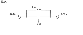
- FIG. 2A is a diagram for explaining the principle of the present invention.
- FIG. 2B is a diagram for explaining the principle of the present invention.
- FIG. 3A is a diagram for explaining the principle of the present invention.
- FIG. 3B is a diagram for explaining the principle of the present invention.
- FIG. 4A is a diagram for explaining the principle of the present invention.
- FIG. 4B is a diagram for explaining the principle of the present invention.
- FIG. 5 is a circuit configuration diagram of the filter according to Comparative Example 1.
- FIG. 6 is a graph comparing the pass characteristics of the filter according to the first embodiment and the pass characteristics of the filter according to the first comparative example.
- FIG. 7 is a circuit configuration diagram of a filter according to Comparative Example 2.
- FIG. 8A is a graph showing a comparison between the pass characteristics of the filter (low-pass filter) according to the first embodiment and the pass characteristics of the filter (low-pass filter) according to Comparative Example 2.
- FIG. 8B is a graph showing a comparison between the pass characteristic of the filter (high-pass filter) according to the first embodiment and the pass characteristic of the filter (high-pass filter) according to the second comparative example.
- FIG. 9 is a circuit configuration diagram of the filter according to the second embodiment.
- FIG. 10A is a graph comparing the pass characteristics of the filter (low-pass filter) according to the second embodiment and the pass characteristics of the filter (low-pass filter) according to the second comparative example.
- FIG. 10B is a graph showing a comparison between the pass characteristics of the filter (high-pass filter) according to the second embodiment and the pass characteristics of the filter (high-pass filter) according to the second comparative example.
- FIG. 11 is a circuit configuration diagram of the filter according to the third embodiment.
- FIG. 12 is a graph showing a comparison between the pass characteristic of the filter according to the third embodiment and the pass characteristic of the filter according to the second comparative example.
- FIG. 13 is a circuit configuration diagram of the multiplexer according to the fourth embodiment.
- FIG. 14 is a circuit configuration diagram of a multiplexer according to Comparative Example 3.
- FIG. 15 is a graph comparing the pass characteristics of the multiplexer according to the fourth embodiment and the pass characteristics of the multiplexer according to the third comparative example.
- FIG. 16 is a circuit configuration diagram of the multiplexer according to the fifth embodiment.
- FIG. 17 is a graph comparing the pass characteristics of the multiplexer according to the fifth embodiment and the pass characteristics of the multiplexer according to the third comparative example.
- FIG. 18 is a circuit configuration diagram of the multiplexer according to the sixth embodiment.
- FIG. 19 is a circuit configuration diagram of a multiplexer according to Comparative Example 4.
- FIG. 20 is a graph comparing the pass characteristics of the multiplexer according to the sixth embodiment and the pass characteristics of the multiplexer according to the fourth comparative example.
- FIG. 21 is a circuit configuration diagram of the multiplexer according to the seventh embodiment.
- FIG. 22 is a graph illustrating pass characteristics of the multiplexer according to the seventh embodiment.
- FIG. 23 is a circuit configuration diagram of the multiplexer according to the eighth embodiment.
- FIG. 24 is a graph illustrating pass characteristics of the multiplexer according to the eighth embodiment.
- FIG. 25 is a circuit configuration diagram of the multiplexer according to the ninth embodiment.
- FIG. 26 is a graph illustrating pass characteristics of the multiplexer according to the ninth embodiment.
- FIG. 27 is a circuit configuration diagram of the multiplexer according to the tenth embodiment.
- FIG. 28 is a circuit configuration diagram of the multiplexer according to the eleventh embodiment.
- FIG. 29 is a graph illustrating pass characteristics of the multiplexer according to the eleventh embodiment.
- FIG. 30 is a diagram for explaining the reason that each resonator constituting the multiplexer according to the fourth embodiment can be formed with one chip.
- FIG. 30 is a diagram for explaining the reason that each resonator constituting the multiplexer according to the fourth embodiment can be formed with one chip.
- FIG. 31 is a diagram for explaining the reason that each resonator forming the multiplexer according to the sixth embodiment can be formed by one chip.
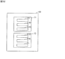
- FIG. 32 is a top view schematically illustrating the structure of the multiplexer according to the sixth embodiment.
- FIG. 33 is a circuit configuration diagram of a filter according to a modification of the first embodiment.
- FIG. 34 is a graph illustrating pass characteristics of the filter according to the modification of the first embodiment when the switch is off and on.
- FIG. 35 is a circuit configuration diagram of the high-frequency front-end circuit according to the second embodiment.
- FIG. 36 is a circuit configuration diagram of the communication device according to the second embodiment.
- the high frequency filter is also referred to as a filter.
- the filter according to the first embodiment includes two first impedance elements connected in series on a path connecting the input terminal and the output terminal, and a second second impedance element connected in parallel to a series circuit of the two first impedance elements.
- the first impedance element is one of a capacitor and an inductor
- the second impedance element is the other of a capacitor and an inductor. That is, when the first impedance element is a capacitor, the second impedance element is an inductor, and when the first impedance element is an inductor, the second impedance element is a capacitor.
- an LC resonance circuit (specifically, an LC parallel resonance circuit) is configured by the two first impedance elements and the second impedance element. Further, the LC resonance circuit can function as both a high-pass filter and a low-pass filter by appropriately setting the respective element values (capacitance value, inductance value) of the two first impedance elements and the second impedance element. .
- the capacitor according to the present invention is an element that exhibits capacitance in all bands as an ideal element, and does not include an elastic wave resonator. This is because the elastic wave resonator exhibits inductive properties in a band between the resonance frequency and the anti-resonance frequency, and exhibits capacitive properties in other bands, but is not an element exhibiting capacitive properties in all bands.
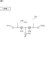
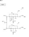
- FIG. 1 is a circuit configuration diagram of the filter 10 according to the first embodiment.
- the filter 10 includes capacitors C1a and C1b, an inductor L2, and a parallel arm resonator P1.
- the capacitors C1a and C1b are two first impedance elements connected in series on a path connecting the terminal 101a and the terminal 102a.
- the terminal 101a is described as an input terminal, and the terminal 102a is described as an output terminal.
- the terminal 101a may be an output terminal, or the terminal 102a may be an input terminal.
- the inductor L2 is a second impedance element connected in parallel to a series circuit of the capacitors C1a and C1b. Specifically, the inductor L2 is connected between a connection point between the capacitor C1a and the terminal 101a and a connection point between the capacitor C1b and the terminal 102a.
- the LC resonance circuit 11 is formed by the capacitors C1a and C1b and the inductor L2.
- an LC resonance circuit is formed by two first impedance elements, one of the capacitor and the inductor, and a second impedance element, the other of the capacitor and the inductor.
- the dashed lines surrounding these and the description of “LC resonance circuit” are omitted.
- the parallel arm resonator P1 is an elastic wave resonator connected between the node N on the path connecting the terminal 101a and the terminal 102a between the capacitors C1a and C1b and the ground.
- the elastic wave resonator is a resonator using an elastic wave, for example, a resonator using SAW (Surface Acoustic Wave), a resonator using a BAW (Bulk Acoustic Wave), or an FBAR (Film Bulk Acoustic Resonator). ).
- SAW Surface Acoustic Wave
- BAW Bulk Acoustic Wave
- FBAR Fanm Bulk Acoustic Resonator
- SAW Surface Acoustic Wave
- the elastic wave resonator is a SAW resonator.
- the elastic wave resonator constituting the filter 10 can be constituted by an IDT (Inter Digital Transducer) electrode formed on a substrate having piezoelectricity, a small and low-profile filter circuit having high steep attenuation characteristics. Can be realized.
- IDT Inter Digital Transducer
- the substrate having piezoelectricity is a substrate having piezoelectricity on at least the surface.
- the substrate may include, for example, a piezoelectric thin film on the surface, a film having a different sound speed from the piezoelectric thin film, and a laminate such as a support substrate.
- the substrate is, for example, a high-sonic support substrate, a laminate including a piezoelectric thin film formed on the high-sonic support substrate, a high-sonic support substrate, and a low-sonic film formed on the high-sonic support substrate.
- a laminate including a piezoelectric thin film formed on a low-sonic film, or a supporting substrate, a high-sonic film formed on the supporting substrate, a low-sonic film formed on the high-sonic film, and a low-sonic It may be a laminate including a piezoelectric thin film formed on the film.
- the substrate may have piezoelectricity over the entire substrate. The same applies to the elastic wave resonators (series arm resonators and parallel arm resonators) described in the second to sixth embodiments, and the description is omitted in the second to sixth embodiments.
- a parallel arm resonator P1 is connected between capacitors C1a and C1b (two first impedance elements) constituting the LC resonance circuit 11, as shown in FIG. The principle of this will be described with reference to FIGS. 2A to 4B.
- [principle] 2A to 4B are views for explaining the principle of the present invention.
- FIG. 2A is a diagram illustrating a filter (LC resonance circuit) including the capacitor C1b and the inductor L2, in which the capacitor C1a and the parallel arm resonator P1 are removed from the configuration of the filter 10.
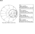
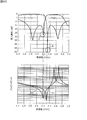
- FIG. 2B is a Smith chart showing the impedance characteristics of the filter shown in FIG. 2A.
- the Smith charts showing the impedance characteristics described in FIG. 2B, FIG. 3B and FIG. 4B show the vicinity of the lower end and the upper end of the required pass band, and the vicinity of the lower end of the required attenuation band. And a marker is added near the high frequency end.
- the frequency, the magnitude ⁇ and the phase ⁇ of the reflection coefficient, and the impedance (*) at the marker m * (where * is a numerical value following m in the graph) in the graph are shown.
- the coefficient Z0 is, for example, 50 ⁇ ).
- the required pass band is from 2300 MHz (frequency at marker m3) to 2690 MHz (frequency at marker m4)
- the required attenuation band is from 1710 MHz (frequency at marker m1) to 1920 MHz (frequency at marker m2).
- the filter shown in FIG. 2A is, for example, a high-pass filter in order to realize the required pass band and attenuation band, and as shown in FIG. 2B, near the low end and high end of the pass band. Is close to 50 ⁇ , and the impedance near the low end and high end of the attenuation band is almost open.
- the vicinity of the low end and the vicinity of the high end (markers m3 and m4) of the pass band are surrounded by broken-line circles, and the vicinity of the low end and high end of the attenuation band (markers m1 and m2). ) Is surrounded by a dot-dash line circle.
- the filter shown in FIG. 2A is an LC resonance circuit including the capacitor C1b and the inductor L2, it is difficult to obtain steep attenuation characteristics. On the other hand, it is conceivable to obtain a steep damping characteristic by adding an elastic wave resonator having a steep damping pole.
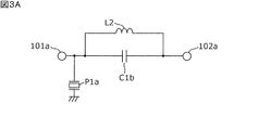
- FIG. 3A is a diagram in which a parallel arm resonator P1a is added to the configuration of the filter shown in FIG. 2A, and shows a filter including a capacitor C1b, an inductor L2, and a parallel arm resonator P1a.
- the parallel arm resonator P1a is connected between the node between the connection point of the capacitor C1b and the inductor L2 connected in parallel and the terminal 101a, and the ground.
- the parallel arm resonator P1a is a resonator having a resonance frequency of 2200 MHz and an anti-resonance frequency of 2500 MHz. Therefore, the parallel arm resonator P1a shows inductive properties in the resonance bandwidth (2200 MHz to 2500 MHz) and shows capacitive properties in other bands.
- FIG. 3B is a Smith chart showing the impedance characteristics of the filter shown in FIG. 3A.
- FIG. 3B shows a dot-dash line circle at the same position as the markers m1 and m2 shown in FIG. 2B. 2B, the same positions as the markers m3 and m4 are indicated by broken-line circles.
- the position of the marker m3 is shifted from the position of the dashed circle by adding the parallel arm resonator P1a exhibiting inductive properties at the frequency. Rotate clockwise (direction of arrow A).
- the frequency at the marker m4 near the high-frequency end of the passband is 2690 MHz
- the position of the marker m4 is indicated by a broken-line circle due to the addition of the parallel arm resonator P1a showing the capacitance at the frequency. Rotate clockwise from the position (direction of arrow B).
- the pass band from 2300 MHz to 2690 MHz, from the center (50 ⁇ ) of the Smith chart, The separated bands increase, and the insertion loss in the pass band increases.
- the parallel arm resonator P1a showing the capacitance at these frequencies is As a result of the addition, the positions of the markers m1 and m2 rotate in the clockwise direction (the direction of arrow C) from the position of the dashed-dotted circle. As described above, the attenuation band from 1710 MHz to 1920 MHz is apart from the open position of the Smith chart, and the attenuation characteristic is deteriorated.
- FIG. 4A is a diagram showing a filter in which a capacitor C1a is connected in series to a capacitor C1b in the configuration of the filter shown in FIG. 2A, and a parallel arm resonator P1 is connected between a node between the capacitors C1a and C1b and ground. is there.
- FIG. 4B is a Smith chart showing the impedance characteristics of the filter shown in FIG. 4A.
- FIG. 9 is a graph showing a change in impedance characteristics due to the addition of the capacitor C1a and the parallel arm resonator P1 to the filter shown in FIG. 2A (specifically, the addition of the capacitor C1a and the parallel arm resonator P1 in this order).
- a dashed-dotted circle is provided at the same position as the markers m1 and m2 shown in FIG. 2B, and a dashed-dotted circle is provided at the same position as the markers m3 and m4 shown in FIG.
- the parallel arm resonator P1 is a resonator having a resonance frequency of 2200 MHz and an anti-resonance frequency of 2500 MHz, like the parallel arm resonator P1a. For this reason, the parallel arm resonator P1 shows inductive properties in the resonance bandwidth (2200 MHz to 2500 MHz) and shows capacitive properties in other bands.
- the position of each marker rotates in the counterclockwise direction because the capacitor C1a showing the capacitance in all bands is connected in series to the capacitor C1b.
- the positions of the markers m3 and m4 rotate in the direction of arrow A from the position of the dashed circle and move to the vicinity of the position of the two-dot chain line circle.
- the positions of the markers m1 and m2 rotate in the direction of arrow B from the position of the dot-dash line circle. Note that the positions of the markers m1 and m2 are originally near the open position, and do not move greatly on the Smith chart even if the capacitor C1a is added. It is not shown like a two-dot chain line circle.
- the position of the marker m3 is changed to the position indicated by the two-dot chain line circle due to the addition of the parallel arm resonator P1 exhibiting inductive properties at the frequency. From the counterclockwise direction (direction of arrow C).
- the frequency at the marker m4 near the high-frequency end of the passband is 2690 MHz
- the position of the marker m4 is indicated by the two-dot chain line due to the addition of the parallel arm resonator P1 showing the capacitance at the frequency. It rotates clockwise (direction of arrow D) from the position of the circle.
- the positions of the markers m3 and m4 which were within the dashed circle were once rotated in the direction of arrow A by the capacitor C1a. It is considered that by rotating the markers m3 and m4 by P1, it was possible to approach the center of the Smith chart. Therefore, an increase in insertion loss in the pass band can be suppressed.
- the capacitance value of the capacitor C1a (that is, rotation in the direction of arrow A) is set so that the impedance at the markers m3 and m4 (that is, in the pass band) after the addition of the parallel arm resonator P1 is located near the center of the Smith chart. Volume) has been adjusted.
- the frequency of the marker m1 near the lower end of the attenuation band is 1710 MHz
- the frequency of the marker m2 near the higher end is 1920 MHz.
- the positions of the markers m1 and m2 rotate in the clockwise direction (the direction of arrow E) from the position of the dashed-dotted circle.
- the positions of the markers m1 and m2 which were within the dashed-dotted circle were once rotated in the direction of arrow B by the capacitor C1a. Even if m2 and m2 are rotated in the direction of arrow E, the Smith chart can be kept away from the open position. Therefore, the deterioration of the attenuation characteristic can be suppressed.
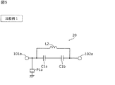
- FIG. 5 is a circuit configuration diagram of the filter 20 according to Comparative Example 1.
- the filter 20 according to Comparative Example 1 is different from the filter 10 according to Example 1 in the position where the parallel arm resonator is connected.
- the other points are the same as those in the filter 10, and the description is omitted.
- the parallel arm resonator P1a is connected between the ground between a node between the LC resonance circuit including the capacitors C1a and C1b and the inductor L2 and the terminal 101a and the ground. That is, in the filter 20, the parallel arm resonator P1a is not connected between the capacitors C1a and C1b as in the first embodiment, and has a configuration similar to that of the filter illustrated in FIG. 3A.
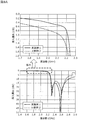
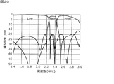
- FIG. 6 is a graph showing a comparison between the pass characteristic of the filter 10 according to the first embodiment and the pass characteristic of the filter 20 according to the first comparative example.
- the graph shown on the upper side of FIG. 6 is an enlarged view around the broken line circle of the graph shown on the lower side. It should be noted that the same applies to the subsequent diagrams showing the passing characteristics, in which the dashed circle indicates “enlarged”.
- the solid line indicates the pass characteristic of the filter 10 according to the first embodiment
- the broken line indicates the pass characteristic of the filter 20 according to the first comparative example.
- FIG. 6 is a graph showing pass characteristics when the filters 10 and 20 are designed to function as high-pass filters.
- the filters 10 and 20 include an elastic wave resonator, and both have steep attenuation characteristics as shown in FIG. 6 due to the steep attenuation pole caused by the elastic wave resonator.
- the filter 10 can suppress an increase in insertion loss in the pass band (2300 MHz to 2690 MHz) as compared with the filter 20.
- the insertion loss at 2300 MHz is 1.191 dB for the filter 20, while the filter 10 is as small as 0.838 dB for the filter 20, and the insertion loss at 2690 MHz is 4.216 dB for the filter 20.
- the filter 10 is as small as 1.391 dB.
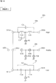
- FIG. 7 is a circuit configuration diagram of the filter 20a according to Comparative Example 2.
- the filter 20a according to Comparative Example 2 includes the series arm resonators S10 and S20, the inductor L20, and the parallel arm resonator P10.
- the series arm resonators S10 and S20 are connected in series on a path connecting the terminal 101a and the terminal 102a.
- the inductor L20 is connected in parallel to the series circuit of the series arm resonators S10 and S20. Specifically, the inductor L20 is connected between a connection point between the series arm resonator S10 and the terminal 101a and a connection point between the series arm resonator S20 and the terminal 102a.
- the parallel arm resonator P10 is an elastic wave resonator connected between a node on the path connecting the terminal 101a and the terminal 102a between the series arm resonators S10 and S20 and the ground.
- the filter 20a according to the comparative example 2 is a ladder-type filter in which the series arm resonators S10 and S20 are connected instead of the two capacitors C1a and C1b, and the elastic wave resonators are arranged in a ladder-type. 1 is different from the filter 10 according to the first embodiment. Note that the element parameters of the series arm resonators S10 and S20, the inductor L20, and the parallel arm resonator P10 are adjusted such that the filter 20a has a pass band equivalent to that of the filter 10.
- the elastic wave resonator exhibits a capacitive characteristic in a band other than between the resonance frequency and the anti-resonance frequency, and can be used as a substitute for a capacitor. That is, it is considered that the function of the filter 10 according to the first embodiment can also be realized by the filter 20a according to the second comparative example.
- the pass band of the ladder-type filter is limited by the resonance bandwidth of each elastic wave resonator. Therefore, by giving Comparative Example 2 as a comparative object of Example 1, it is possible to confirm how excellent the pass characteristic of the filter of the present invention is compared with the ladder type filter.
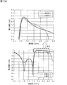
- FIG. 8A is a graph showing a comparison between pass characteristics of the filter 10 (low-pass filter) according to the first embodiment and pass characteristics of the filter 20a (low-pass filter) according to the second comparative example.
- the solid line indicates the pass characteristic of the filter 10 according to the first embodiment
- the broken line indicates the pass characteristic of the filter 20a according to the second comparative example.
- the filter 10 and the filter 20a include an elastic wave resonator, and both have a steep attenuation characteristic as shown in FIG. 8A due to a steep attenuation pole caused by the elastic wave resonator.
- the filter 10 can suppress an increase in insertion loss in the pass band as compared with the filter 20a. Specifically, the insertion loss at 2200 MHz is as small as 0.792 dB for the filter 10 while the filter 20a is 1.561 dB for the filter 20a.
- FIG. 8B is a graph comparing the pass characteristics of the filter 10 (high-pass filter) according to the first embodiment and the pass characteristics of the filter 20a (high-pass filter) according to the second comparative example.
- the solid line indicates the pass characteristic of the filter 10 according to the first embodiment
- the broken line indicates the pass characteristic of the filter 20a according to the second comparative example.
- the filter 10 and the filter 20a each include an elastic wave resonator, and both have steep attenuation characteristics as shown in FIG. 8B due to the steep attenuation pole of the elastic wave resonator.
- the filter 10 can suppress an increase in insertion loss in the pass band (2300 MHz to 2690 MHz) as compared with the filter 20a. Specifically, the insertion loss at 2300 MHz is 0.94 dB for the filter 20a, whereas the filter 10 is as small as 0.922 dB for the filter 20a, and the insertion loss at 2690 MHz is 1.483 dB for the filter 20a. On the other hand, the filter 10 is as small as 1.1 dB.
- the ladder-type filter using the elastic wave resonator instead of the capacitors C1a and C1b has deteriorated transmission characteristics. That is, when the LC resonance circuit is configured as in the present invention, the deterioration of the transmission characteristic can be suppressed by not using the elastic wave resonator instead of the capacitor.
- the filter 10 having a steep attenuation characteristic and having a low-loss passband which is not limited to the resonance bandwidth (for example, 300 MHz or the like) of the elastic wave resonator like a ladder filter. .
- FIG. 9 is a circuit configuration diagram of the filter 10a according to the second embodiment.
- the filter 10a includes inductors L1a and L1b, a capacitor C2, and a parallel arm resonator P2.
- the inductors L1a and L1b are two first impedance elements connected in series on a path connecting the terminal 101a and the terminal 102a.
- the capacitor C2 is a second impedance element connected in parallel to a series circuit of the inductors L1a and L1b. Specifically, the capacitor C2 is connected between a connection point between the inductor L1a and the terminal 101a and a connection point between the inductor L1b and the terminal 102a.
- the second embodiment differs from the first embodiment in that the two first impedance elements are inductors and the second impedance element is a capacitor.
- an LC resonance circuit is formed by the inductors L1a and L1b and the capacitor C2.
- the parallel arm resonator P2 is an elastic wave resonator connected between a node on a path connecting the terminals 101a and 102a between the inductors L1a and L1b and the ground.
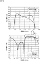
- FIG. 10A is a graph showing a comparison between the pass characteristic of the filter 10a (low-pass filter) according to the second embodiment and the pass characteristic of the filter 20a (low-pass filter) according to the second comparative example.
- the solid line indicates the pass characteristic of the filter 10a according to the second embodiment
- the broken line indicates the pass characteristic of the filter 20a according to the second comparative example.
- the filters 10a and 20a each include an elastic wave resonator, and both have steep attenuation characteristics as shown in FIG. 10A due to the steep attenuation pole caused by the elastic wave resonator.
- the filter 10a can suppress an increase in insertion loss in the pass band as compared with the filter 20a.
- the insertion loss at 2200 MHz is 1.561 dB for the filter 20a, and 0.825 dB for the filter 10a.
- FIG. 10B is a graph showing a comparison between the pass characteristic of the filter 10a (high-pass filter) according to the second embodiment and the pass characteristic of the filter 20a (high-pass filter) according to the second comparative example.
- the solid line indicates the pass characteristic of the filter 10a according to the second embodiment
- the broken line indicates the pass characteristic of the filter 20a according to the second comparative example.
- the filters 10a and 20a each include an elastic wave resonator, and as shown in FIG. 10B, both have steep attenuation characteristics due to a steep attenuation pole of the elastic wave resonator.
- the filter 10a can suppress an increase in insertion loss in a pass band (2300 MHz to 2690 MHz) as compared with the filter 20a. Specifically, the insertion loss at 2300 MHz is 0.94 dB for the filter 20a, whereas the filter 10a is as small as 0.838 dB, and the insertion loss at 2690 MHz is 1.483 dB for the filter 20a. On the other hand, the filter 10a is as small as 1.391 dB.
- the filter 10a having a steep attenuation characteristic and having a low-loss passband.
- FIG. 11 is a circuit configuration diagram of the filter 10b according to the third embodiment.
- the filters according to the first and second embodiments may further include a third impedance element connected in parallel to one of the two first impedance elements.
- the third impedance element is a capacitor.
- the third impedance element is an inductor.
- a filter in which the first impedance element is an inductor and the third impedance element is a capacitor specifically, a capacitor C3 is connected in parallel to the inductor L1a (first impedance element) in the second embodiment.
- the filter 10b will be described.
- the filter 10b includes a capacitor C3 in addition to the configuration of the filter 10a according to the second embodiment.
- the other points are the same as those in the second embodiment, and the description is omitted.
- the capacitor C3 is connected in parallel with the inductor L1a. Note that the capacitor C3 may be connected in parallel with the inductor L1b instead of the inductor L1a.
- FIG. 12 is a graph showing a comparison between the pass characteristic of the filter 10b according to the third embodiment and the pass characteristic of the filter 20a according to the second comparative example.
- the solid line indicates the pass characteristic of the filter 10b according to the third embodiment
- the broken line indicates the pass characteristic of the filter 20a according to the second comparative example.
- FIG. 12 is a graph showing pass characteristics when the filters 10b and 20a are designed to function as high-pass filters.
- the filters 10b and 20a include elastic wave resonators, and both have steep attenuation characteristics as shown in FIG. 12 due to the steep attenuation pole of the elastic wave resonator.
- the filter 10b can suppress an increase in the insertion loss in the pass band (2300 MHz to 2690 MHz) as compared with the filter 20a.
- the insertion loss at 2300 MHz is 0.94 dB for the filter 20a
- the filter 10a is as small as 0.907 dB
- the insertion loss at 2690 MHz is 1.483 dB for the filter 20a.
- the filter 10a is as small as 1.314 dB.
- the provision of the capacitor C3 makes it possible to make the impedance close to 50 ⁇ near the high-frequency end of the pass band. Therefore, at 2690 MHz, the insertion loss can be made smaller than in the second embodiment. .
- the filter 10b having a steep attenuation characteristic and having a low-loss passband.
- the capacitor C1a has a steep attenuation characteristic and a low loss. Filter 10 having a wide pass band can be realized.
- the filters according to the first to third embodiments described above can be applied to a multiplexer. Such a multiplexer will be described as Examples 4 to 11.
- the multiplexers according to the fourth to eleventh embodiments specifically include a plurality of filters each including the filters according to the first to third embodiments.
- the multiplexer includes a filter other than a plurality of filters (a third filter in the sixth embodiment, a low-pass filter in the ninth embodiment, and a high-pass filter in the tenth embodiment). ) In some cases. Input terminals or output terminals of the plurality of filters are connected to a common terminal.
- the plurality of filters include at least a first filter and a second filter, and an input terminal or an output terminal of the first filter and an input terminal or an output terminal of the second filter are connected to a common terminal.
- the input terminals of the plurality of filters are connected to the common terminal, but the output terminals may be connected to the common terminal.
- the multiplexer includes filters other than the plurality of filters, input terminals or output terminals of the filters other than the plurality of filters are also connected to the common terminal.
- the multiplexers according to the fourth to eleventh embodiments simultaneously output signals in a plurality of frequency bands respectively corresponding to filters constituting the multiplexer (a filter having an input terminal or an output terminal connected to a common terminal in the multiplexer). Transmission and reception, that is, so-called CA may be supported.
- the plurality of frequency bands corresponding to each of the filters constituting the multiplexer may be, for example, an LTE (Long Term Evolution: 4G) Band or an NR (New Radio: 5G) Band. Good.
- the plurality of frequency bands are, for example, sub @ 6 GHz (n77 (3.3-4.2 GHz), n78 (3.3-3.8 GHz), n79 (4.4-5.0 GHz) as NR Bands. ), 5.0-7.125 GHz).
- Band of 5.0-7.125 GHz for example, Band 46 (5150-5925 MHz) or Band 47 (5855-5925 MHz) is used.
- the plurality of frequency bands may be, for example, L5 of Global Positioning System (GPS).
- GPS Global Positioning System
- the plurality of frequency bands may include a 5 GHz band of Wi-Fi (registered trademark).
- the 5 GHz band may be, for example, 5150-5725 MHz.
- the first filter and the second filter may be filters that include any of these frequency bands in a pass band.
- the multiplexer includes a filter including a pass band of 699 MHz to 960 MHz, a filter including a pass band of 1.2 GHz, a filter including a pass band of 1.4 GHz to 5 GHz, and a pass band of 5 GHz to 7.125 GHz. And at least two filters. Further, for example, the multiplexer includes a filter including a pass band of 699 MHz to 2.7 GHz, a filter including a pass band of 3.3 GHz to 4.2 GHz, a filter including a pass band of 4.4 GHz to 5 GHz, and a filter including a pass band of 4.4 GHz to 5 GHz. At least two filters may be included among filters having a pass band of 7.125 GHz.
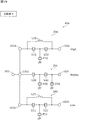
- FIG. 13 is a circuit configuration diagram of the multiplexer 30 according to the fourth embodiment.
- the plurality of filters in the multiplexer 30 include the first filter and the second filter as the filters according to the first to third embodiments.
- the multiplexer 30 is a diplexer including two filters according to the first embodiment.
- the two filters according to the first embodiment are filters 10 and 10d.
- the filter 10d is a first filter
- the filter 10 is a second filter.
- the filter 10d includes capacitors C1c and C1d, an inductor L5, and a parallel arm resonator P3.
- the capacitors C1c and C1d are two first impedance elements connected in series on a path connecting the terminal 101a and the terminal 102a.
- the inductor L5 is a second impedance element connected in parallel to a series circuit of the capacitors C1c and C1d. Specifically, the inductor L5 is connected between a connection point between the capacitor C1c and the terminal 101a and a connection point between the capacitor C1d and the terminal 102a.
- the parallel arm resonator P3 is an elastic wave resonator connected between the ground and a node on a path connecting the terminals 101a and 102a between the capacitors C1c and C1d.
- the filter 10d has the same configuration as the filter 10 of the first embodiment.
- the first impedance element included in the filter 10d and the first impedance element included in the filter 10 are both capacitors.
- the terminal 101b is, for example, an input terminal, and the terminal 102b is, for example, an output terminal.
- the input terminal (terminal 101a) of the filter 10d and the input terminal (terminal 101b) of the filter 10 are commonly connected to the common terminal 103.
- the common terminal 103 and the terminals 101a and 101b may be directly connected without interposing any other element or the like, or may be indirectly connected with another element.
- the filter 10d is a high-pass filter
- the filter 10 is a low-pass filter
- the pass band of the filter 10d is higher than the pass band of the filter 10.
- the multiplexer 30 can support two frequency bands. In FIG. 13, “High” is described next to the terminal 102 a of the filter 10 d and “Low” is described next to the terminal 102 b of the filter 10 because the pass band of the filter 10 d It is higher than the band.
- FIG. 14 is a circuit configuration diagram of the multiplexer 40 according to Comparative Example 3.
- the multiplexer 40 is a diplexer including two filters according to Comparative Example 2.
- the two filters according to Comparative Example 2 are filters 20a and 20b.
- the configuration of the filter 20b is the same as that of the filter 20a, the description is omitted.
- the filter 20a is a high-pass filter
- the filter 20b is a low-pass filter.
- the pass band of the filter 20a is higher than the pass band of the filter 20b.
- "High” is described next to the terminal 102a of the filter 20a
- "Low” is described next to the terminal 102b of the filter 20b because the pass band of the filter 20a is higher than that of the filter 20b. It is higher than the band.
- the element values of the filter 20a are set so that the filter 20a has the same pass band as the filter 10d
- the element values of the filter 20b are set so that the filter 20b has the same pass band as the filter 10. Have been.
- FIG. 15 is a graph comparing the pass characteristics of the multiplexer 30 according to the fourth embodiment and the pass characteristics of the multiplexer 40 according to the third comparative example.
- the solid line indicates the pass characteristic of the multiplexer 30 according to the fourth embodiment
- the broken line indicates the pass characteristic of the multiplexer 40 according to the third comparative example.
- “High” is described in the pass band formed by the filter 10 d configuring the multiplexer 30 and the filter 20 a configuring the multiplexer 40.
- “Low” is described in a pass band formed by the filter 10 forming the multiplexer 30 and the filter 20 b forming the multiplexer 40.
- Each of the filters 10d and 20a includes an elastic wave resonator. Due to a steep attenuation pole caused by the elastic wave resonator, each of the multiplexers has a steep attenuation characteristic at the lower end of the pass band indicated by “High” in FIG. Have. Each of the filters 10 and 20b also includes an elastic wave resonator. Due to the steep attenuation pole caused by the elastic wave resonator, each of the multiplexers is steep at the high-frequency end of the pass band indicated by “Low” in FIG. It has attenuation characteristics. On the other hand, the multiplexer 30 can suppress an increase in insertion loss in the pass band as compared with the multiplexer 40.
- the insertion loss at 2200 MHz is 1.806 dB for the multiplexer 40 and 1.226 dB for the multiplexer 30.
- the insertion loss at 2300 MHz is 1.778 dB in the multiplexer 40
- the multiplexer 30 is as small as 1.217 dB.
- the insertion loss at 2690 MHz is 1.02 dB in the multiplexer 40.
- the multiplexer 30 is as small as 0.788 dB.
- the multiplexer 30 having steep attenuation characteristics and a low-loss passband can be realized.
- the first filter is the filter 10d (the filter according to the first embodiment), but the first filter may be the filter 10a (the filter according to the second embodiment).
- both the first impedance element included in the filter 10d (first filter) and the first impedance element included in the filter 10 (second filter) are capacitors, so that the first filter As compared with the case where the filter 10a is used, a multiplexer having a pass band with lower loss can be realized.
- the inductor has a lower Q value than the capacitor, and by using the filter 10d according to the first embodiment having a smaller number of inductors than the filter 10a according to the second embodiment, the total number of inductors having a low Q value used in the multiplexer is reduced. It is because it becomes less. In other words, the total number of capacitors having a high Q value is increased, and the loss can be reduced.
- FIG. 16 is a circuit configuration diagram of the multiplexer 30a according to the fifth embodiment.
- the multiplexer 30a includes a filter 10b instead of the filter 10d in the multiplexer 30 according to the fourth embodiment.
- the other points are the same as those in the fourth embodiment, and the description is omitted.
- the filter 10b is a high-pass filter
- the filter 10 is a low-pass filter
- the pass band of the filter 10b is higher than the pass band of the filter 10.
- the multiplexer 30a can support two frequency bands. In FIG. 16, “High” is described next to the terminal 102 a of the filter 10 b and “Low” is described next to the terminal 102 b of the filter 10 because the pass band of the filter 10 b It is higher than the band.
- FIG. 17 is a graph comparing the pass characteristics of the multiplexer 30a according to the fifth embodiment and the pass characteristics of the multiplexer 40 according to the third comparative example.
- the solid line indicates the pass characteristic of the multiplexer 30a according to the fifth embodiment
- the broken line indicates the pass characteristic of the multiplexer 40 according to the third comparative example.
- “High” is described in the pass band formed by the filter 10 b forming the multiplexer 30 a and the filter 20 a forming the multiplexer 40.
- “Low” is described in the pass band formed by the filter 10 forming the multiplexer 30a and the filter 20b forming the multiplexer 40.
- Each of the filters 10b and 20a includes an elastic wave resonator. Due to a steep attenuation pole caused by the elastic wave resonator, each of the multiplexers has a steep attenuation characteristic at a lower end of a pass band indicated by “High” in FIG. Have. Each of the filters 10 and 20b also includes an elastic wave resonator. Due to a steep attenuation pole caused by the elastic wave resonator, each of the multiplexers is steep at the high-frequency end of the pass band indicated by “Low” in FIG. It has attenuation characteristics. On the other hand, the multiplexer 30a can suppress an increase in insertion loss in the pass band as compared with the multiplexer 40.
- the insertion loss at 2200 MHz is 1.806 dB for the multiplexer 40 and 1.05 dB for the multiplexer 30a.
- the multiplexer 30 has an insertion loss of 1.778 dB at 2300 MHz, the multiplexer 30 has a low insertion loss of 1.074 dB, and the insertion loss at 2690 MHz has a multiplexer of 1.02 dB.
- the multiplexer 30 is as small as 0.897 dB.
- the multiplexer 30a having a steep attenuation characteristic and having a low-loss passband.
- FIG. 18 is a circuit configuration diagram of the multiplexer 30b according to the sixth embodiment.
- the plurality of filters in the multiplexer 30b include a first filter and a second filter as the filters according to the first to third embodiments. Further, the multiplexer 30b further includes a third filter whose input terminal or output terminal is connected to the common terminal. The third filter includes at least one series arm resonator and at least one parallel arm resonator. Specifically, the multiplexer 30b is a triplexer including the filter 10 according to the first embodiment, the filter 10b according to the third embodiment, and the filter 20c. For example, the filter 10b is a first filter, the filter 10 is a second filter, and the filter 20c is a third filter.
- the terminal 101c is, for example, an input terminal
- the terminal 102c is, for example, an output terminal.
- the input terminal (terminal 101a) of the filter 10b, the input terminal (terminal 101c) of the filter 20c, and the input terminal (terminal 101b) of the filter 10 are commonly connected to the common terminal 103.
- the common terminal 103 and the terminals 101a, 101b, and 101c may be directly connected without interposing any other element or the like, or may be indirectly connected through another element. Good.
- the filter 10b is a high-pass filter
- the filter 10 is a low-pass filter
- the filter 20c is a band-pass filter.
- the pass band of the filter 10b is higher than the pass band of the filter 10
- the pass band of the filter 20c is lower than the pass band of the filter 10b and higher than the pass band of the filter 10.
- the multiplexer 30b can support three frequency bands.
- “High” is described next to the terminal 102a of the filter 10b
- “Middle” is described next to the terminal 102c of the filter 20c
- “Low” is described next to the terminal 102b of the filter 10.
- the pass band of the filter 10b is higher than the pass band of the filter 20c
- the pass band of the filter 20c is higher than the pass band of the filter 10.
- the filter 20c includes the series arm resonators S30 and S40 as at least one series arm resonator, and the parallel arm resonators P20 and P30 as at least one parallel arm resonator.
- Series arm resonators S30 and S40 are connected in series on a path connecting terminal 101c and terminal 102c.
- the parallel arm resonator P20 is connected between the node between the series arm resonator S30 and the series arm resonator S40 and the ground
- the parallel arm resonator P30 is connected between the series arm resonator S40 and the terminal 102c. Is connected between this node and the ground.
- the filter 20c may include one or three or more series arm resonators as at least one series arm resonator, and one or three or more parallel arm resonances as at least one parallel arm resonator. A child may be provided.
- FIG. 19 is a circuit configuration diagram of the multiplexer 40a according to Comparative Example 4.
- the multiplexer 40a is a triplexer including the two filters according to the comparative example 2 and the filter 20c.
- two filters according to Comparative Example 2 are filters 20a and 20b.
- the filter 20c in Comparative Example 4 is the same as that in Example 6.
- the filter 20a is a high-pass filter
- the filter 20b is a low-pass filter
- the filter 20c is a band-pass filter.
- the pass band of the filter 20a is higher than the pass band of the filter 20b
- the pass band of the filter 20c is lower than the pass band of the filter 20a and higher than the pass band of the filter 20b.
- “High” is described next to the terminal 102a of the filter 20a
- “Middle” is described next to the terminal 102c of the filter 20c
- “Low” is described next to the terminal 102b of the filter 20b.
- the pass band of the filter 20a is higher than the pass band of the filter 20c, and the pass band of the filter 20c is higher than the pass band of the filter 20b.
- the element values of the filter 20a are set so that the filter 20a has a pass band equivalent to the filter 10b, and the element values of the filter 20b are set so that the filter 20b has a pass band equivalent to the filter 10. Have been.
- FIG. 20 is a graph showing a comparison between the pass characteristics of the multiplexer 30b according to the sixth embodiment and the pass characteristics of the multiplexer 40a according to the fourth comparative example.
- the solid line indicates the pass characteristic of the multiplexer 30b according to the sixth embodiment
- the dashed line indicates the pass characteristic of the multiplexer 40a according to the comparative example 4.
- “High” is described in the pass band formed by the filter 10b forming the multiplexer 30b and the filter 20a forming the multiplexer 40a.
- “Middle” is described in the passband formed by the filters 20c constituting the multiplexers 30b and 40a, respectively.
- “Low” is described in the pass band formed by the filter 10 forming the multiplexer 30b and the filter 20b forming the multiplexer 40a.
- Each of the filters 10b and 20a includes an elastic wave resonator. Due to a steep attenuation pole caused by the elastic wave resonator, each multiplexer has a steep attenuation characteristic at a lower end of a pass band indicated by "High” in FIG. Have. Also, the filters 10 and 20b also include an elastic wave resonator. Due to the steep attenuation pole caused by the elastic wave resonator, each multiplexer is steep at the high-frequency end of the pass band indicated by “Low” in FIG. It has attenuation characteristics. On the other hand, the multiplexer 30b can suppress an increase in insertion loss in the pass band as compared with the multiplexer 40a.
- the insertion loss at 2200 MHz is 1.488 dB for the multiplexer 40a and 1.15 dB for the multiplexer 30b.
- the insertion loss at 2500 MHz is as small as 1.074 dB for the multiplexer 30a, while it is 1.225 dB for the multiplexer 40a.
- the multiplexer 30b having a steep attenuation characteristic and having a low-loss passband.
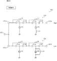
- FIG. 21 is a circuit configuration diagram of the multiplexer 30c according to the seventh embodiment.
- the plurality of filters in the multiplexer 30c include a first filter and a second filter as filters combining the filters according to the first to third embodiments.
- the multiplexer 30c is a diplexer including filters 10e and 10f, and the filters 10e and 10f are filters obtained by combining the filters according to the first and second embodiments, respectively.
- the filter 10f is a first filter
- the filter 10e is a second filter.
- the filter 10e includes capacitors C1a, C1b, C2, inductors L1a, L1b, L10, L11, and parallel arm resonators P1 and P2.
- the capacitors C1a and C1b are two first impedance elements connected in series on a path connecting the terminal 101b and the terminal 102b.
- the inductor L1a is a second impedance element connected in parallel to a series circuit of the capacitors C1a and C1b. Specifically, the inductor L1a is connected between a connection point between the capacitor C1a and the terminal 101b and a connection point between the capacitor C1b and the inductor L1b.
- the parallel arm resonator P1 is an elastic wave resonator connected between a node on a path connecting the terminals 101b and 102b between the capacitors C1a and C1b and the ground.
- the inductor L10 is an inductor connected in series with the parallel arm resonator P1 between the node and the ground.
- the filter composed of the capacitors C1a and C1b, the inductor L1a, and the parallel arm resonator P1 in the filter 10e has the same configuration as the filter 10 of the first embodiment.
- the inductor L1a is also a first impedance element.
- the inductors L1a and L1b are connected in series on a path connecting the terminal 101b and the terminal 102b.
- the inductors L1a and L1b become first impedance elements. It is.
- the capacitor C2 is a second impedance element connected in parallel to a series circuit of the inductors L1a and L1b. Specifically, the capacitor C2 is connected between a connection point between the inductor L1a and the terminal 101b and a connection point between the inductor L1b and the terminal 102b.
- the parallel arm resonator P2 is an elastic wave resonator connected between the ground and a node on a path connecting the terminals 101b and 102b between the inductors L1a and L1b.
- the inductor L11 is an inductor connected in series with the parallel arm resonator P2 between the node and the ground.
- the filter composed of the inductors L1a and L1b, the capacitor C2 and the parallel arm resonator P2 in the filter 10e has the same configuration as the filter 10a of the second embodiment.
- the filter 10f includes capacitors C1c, C1d, and C4, inductors L1c, L1d, L12, and L13, and parallel arm resonators P3 and P4.
- the capacitors C1c and C1d are two first impedance elements connected in series on a path connecting the terminal 101a and the terminal 102a.
- the inductor L1c is a second impedance element connected in parallel to a series circuit of the capacitors C1c and C1d. Specifically, the inductor L1c is connected between a connection point between the capacitor C1c and the terminal 101a and a connection point between the capacitor C1d and the inductor L1d.
- the parallel arm resonator P3 is an elastic wave resonator connected between the ground and a node on a path connecting the terminals 101a and 102a between the capacitors C1c and C1d.
- the inductor L12 is an inductor connected in series with the parallel arm resonator P3 between the node and the ground.
- the filter composed of the capacitors C1c and C1d, the inductor L1c, and the parallel arm resonator P3 in the filter 10f has the same configuration as the filter 10 of the first embodiment.
- the inductor L1c is also a first impedance element.
- the inductors L1c and L1d are connected in series on a path connecting the terminal 101a and the terminal 102a.
- the inductors L1c and L1d become first impedance elements. It is.
- the capacitor C4 is a second impedance element connected in parallel to a series circuit of the inductors L1c and L1d. Specifically, the capacitor C4 is connected between a connection point between the inductor L1c and the terminal 101a and a connection point between the inductor L1d and the terminal 102a.
- the parallel arm resonator P4 is an elastic wave resonator connected between a ground and a node on a path connecting the terminals 101a and 102a between the inductors L1c and L1d.
- the inductor L13 is an inductor connected in series with the parallel arm resonator P4 between the node and the ground.
- the filter composed of the inductors L1c and L1d, the capacitor C4, and the parallel arm resonator P4 in the filter 10f has the same configuration as the filter 10a of the second embodiment.
- the input terminal (terminal 101a) of the filter 10f and the input terminal (terminal 101b) of the filter 10e are commonly connected to the common terminal 103.
- the common terminal 103 and the terminals 101a and 101b may be directly connected without interposing any other element or the like, or may be indirectly connected with another element.
- the filter 10f is a high-pass filter
- the filter 10e is a low-pass filter
- the pass band of the filter 10f is higher than the pass band of the filter 10e.
- the multiplexer 30c can support two frequency bands. In FIG. 21, “High” is described next to the terminal 102 a of the filter 10 f and “Low” is described next to the terminal 102 b of the filter 10 e because the pass band of the filter 10 f is higher than the pass band of the filter 10 e. It is higher than the band.
- FIG. 22 is a graph showing the pass characteristics of the multiplexer 30c according to the seventh embodiment.
- "High” is described in the pass band formed by the filter 10f included in the multiplexer 30c.
- “Low” is described in the pass band formed by the filter 10 e that configures the multiplexer 30 c.
- the filter 10f includes an elastic wave resonator, and the multiplexer 30c has a steep attenuation characteristic at the lower end of the pass band indicated by “High” in FIG. 22 due to the steep attenuation pole caused by the elastic wave resonator. I have. Further, the filter 10e also includes an elastic wave resonator, and the steep attenuation pole by the elastic wave resonator causes the multiplexer 30c to exhibit a steep attenuation characteristic at a high-frequency end of a pass band indicated by “Low” in FIG. Have.
- the insertion loss of the multiplexer 30c at 1430 MHz, 1880 MHz, 2200 MHz, 2300 MHz and 2690 MHz is as small as 0.81 dB, 0.44 dB, 1.47 dB, 1.44 dB and 1.15 dB, respectively.
- the multiplexer 30c having a steep attenuation characteristic and having a low-loss passband.
- FIG. 23 is a circuit configuration diagram of a multiplexer 30d according to the eighth embodiment.
- the plurality of filters in the multiplexer 30d include a first filter and a second filter as filters combining the filters according to the first to third embodiments.
- the multiplexer 30d is a diplexer including filters 10g and 10h, and each of the filters 10g and 10h is a filter in which two filters similar to the filter 10 of the first embodiment are connected in series.
- the filter 10h is a first filter
- the filter 10g is a second filter.
- the filter 10g includes capacitors C1a, C1b, C1e, C1f, inductors L2, L6, L14, and parallel arm resonators P1 and P4.
- the capacitors C1a and C1b are two first impedance elements connected in series on a path connecting the terminal 101b and the terminal 102b.
- the inductor L2 is a second impedance element connected in parallel to a series circuit of the capacitors C1a and C1b. Specifically, the inductor L2 is connected between a connection point between the capacitor C1a and the terminal 101b and a connection point between the capacitor C1b and the capacitor C1e.
- the parallel arm resonator P1 is an elastic wave resonator connected between a node on a path connecting the terminals 101b and 102b between the capacitors C1a and C1b and the ground.
- the filter composed of the capacitors C1a and C1b, the inductor L2, and the parallel arm resonator P1 in the filter 10g has the same configuration as the filter 10 of the first embodiment.
- the capacitors C1e and C1f are two first impedance elements connected in series on a path connecting the terminal 101b and the terminal 102b.
- the inductor L6 is a second impedance element connected in parallel to a series circuit of the capacitors C1e and C1f. Specifically, the inductor L6 is connected between a connection point between the capacitors C1e and C1b and a connection point between the capacitor C1f and the terminal 102b.
- the parallel arm resonator P4 is an elastic wave resonator connected between the ground and a node on a path connecting the terminals 101b and 102b between the capacitors C1e and C1f.
- the inductor L14 is an inductor connected in parallel with the parallel arm resonator P4 between the node and the ground.
- the filter composed of the capacitors C1e and C1f, the inductor L6, and the parallel arm resonator P4 in the filter 10g has the same configuration as the filter 10 of the first embodiment.
- the filter 10h includes capacitors C1c, C1d, C1g, C1h, inductors L5, L6, L15, and parallel arm resonators P3 and P5.
- the capacitors C1c and C1d are two first impedance elements connected in series on a path connecting the terminal 101a and the terminal 102a.
- the inductor L5 is a second impedance element connected in parallel to a series circuit of the capacitors C1c and C1d. Specifically, the inductor L5 is connected between a connection point between the capacitor C1c and the terminal 101a and a connection point between the capacitor C1d and the capacitor C1g.
- the parallel arm resonator P3 is an elastic wave resonator connected between the ground and a node on a path connecting the terminals 101a and 102a between the capacitors C1c and C1d.
- the filter composed of the capacitors C1c and C1d, the inductor L5, and the parallel arm resonator P3 in the filter 10h has the same configuration as the filter 10 of the first embodiment.
- the capacitors C1g and C1h are two first impedance elements connected in series on a path connecting the terminal 101a and the terminal 102a.
- the inductor L7 is a second impedance element connected in parallel to the series circuit of the capacitors C1g and C1h. Specifically, the inductor L7 is connected between a connection point between the capacitor C1g and the capacitor C1d and a connection point between the capacitor C1h and the terminal 102a.
- the parallel arm resonator P5 is an elastic wave resonator connected between a node on the path connecting the terminals 101a and 102a between the capacitors C1g and C1h and the ground.
- the inductor L15 is an inductor connected in series with the parallel arm resonator P5 between the node and the ground.
- the filter composed of the capacitors C1g and C1h, the inductor L7, and the parallel arm resonator P5 in the filter 10h has the same configuration as the filter 10 of the first embodiment.
- the input terminal (terminal 101a) of the filter 10h and the input terminal (terminal 101b) of the filter 10g are commonly connected to the common terminal 103.
- the common terminal 103 and the terminals 101a and 101b may be directly connected without interposing any other element or the like, or may be indirectly connected with another element.
- the filter 10h is a high-pass filter
- the filter 10g is a low-pass filter
- the pass band of the filter 10h is higher than the pass band of the filter 10g.
- the multiplexer 30d can support two frequency bands. In FIG. 23, “High” is described next to the terminal 102a of the filter 10h and “Low” is described next to the terminal 102b of the filter 10g because the pass band of the filter 10h is higher than the pass band of the filter 10g. It is higher than the band.
- FIG. 24 is a graph showing the passing characteristic of the multiplexer 30d according to the eighth embodiment.
- “High” is described in the pass band formed by the filter 10 h configuring the multiplexer 30 d.
- “Low” is described in the pass band formed by the filter 10 g configuring the multiplexer 30 d.
- the filter 10h includes an elastic wave resonator, and the multiplexer 30d has a steep attenuation characteristic at the lower end of the pass band indicated by “High” in FIG. 24 due to the steep attenuation pole caused by the elastic wave resonator. I have.
- the filter 10g also includes an elastic wave resonator, and the steep attenuation pole of the elastic wave resonator causes the multiplexer 30d to exhibit a steep attenuation characteristic at the high-frequency end of the pass band indicated by “Low” in FIG. Have.
- the insertion loss of the multiplexer 30d at 1430 MHz, 1880 MHz, 2200 MHz, 2300 MHz and 2690 MHz is as small as 0.89 dB, 0.51 dB, 1.21 dB, 1.21 dB and 0.93 dB, respectively.
- the multiplexer 30d having a steep attenuation characteristic and having a low-loss passband can be realized.
- FIG. 25 is a circuit configuration diagram of a multiplexer 30e according to the ninth embodiment.
- the plurality of filters in the multiplexer 30e include a first filter and a second filter as filters combining the filters according to the first to third embodiments. Further, the multiplexer 30e further includes a low-pass filter whose input terminal or output terminal is connected to the common terminal. Specifically, the multiplexer 30e is a triplexer including the filters 10g, 10i, and 20d, and the filters 10g and 10i are each a filter in which two filters similar to the filter 10 of the first embodiment are connected in series. .
- the filter 20d is a low-pass filter. For example, the filter 10i is a first filter, and the filter 10g is a second filter.
- the multiplexer 30e includes a capacitor C6 and an inductor L17.
- the filter 10g has the same configuration as that described in the eighth embodiment, and a description thereof will be omitted.
- the filter 10i further includes a capacitor C5 and an inductor L16 in addition to the configuration of the filter 10h described in the eighth embodiment.
- the configuration other than the capacitor C5 and the inductor L16 is the same as that of the filter 10h, and thus the description is omitted.
- the capacitor C5 is a capacitor connected between a node on a path connecting the terminal 101a and the terminal 102a between the capacitors C1d and C1g and the ground.
- the inductor L16 is an inductor connected between the ground and a node on a path connecting the terminal 101a and the terminal 102a between the capacitors C1d and C1g.
- the capacitor C5 and the inductor L16 are connected in series.
- the filter 20d includes capacitors C7, C8, C9, C10, and inductors L18 and L19.
- the capacitor C7 and the inductor L18 are connected in parallel with each other, and form a parallel resonance circuit on a path connecting the terminal 101c and the terminal 102c.
- the capacitor C9 and the inductor L19 are connected in parallel with each other, and form a parallel resonance circuit on a path connecting the terminal 101c and the terminal 102c.
- the capacitor C8 is a capacitor connected between the ground and a node on a path connecting the terminal 101c and the terminal 102c between the capacitors C7 and C9.
- the capacitor C10 is a capacitor connected between the ground and a node on a path connecting the terminal 101c and the terminal 102c between the capacitor C9 and the terminal 102c.
- the capacitor C6 is a capacitor provided on a path connecting the common terminal 103 and the terminal 101a (terminal 101b).
- the inductor L17 is an inductor connected between a ground on a node connecting the common terminal 103 and the terminal 101a (terminal 101b) between the capacitor C6 and the terminal 101a (terminal 101b).
- the capacitor C6 and the inductor L17 form a matching circuit.
- the input terminal (terminal 101a) of the filter 10i, the input terminal (terminal 101b) of the filter 10g, and the input terminal (terminal 101c) of the filter 20d are commonly connected to the common terminal 103.
- the common terminal 103 and the terminals 101a, 101b, and 101c may be directly connected without interposing any other element or the like, or may be indirectly connected through another element.
- FIG. 25 illustrates an example in which the common terminal 103 and the terminals 101a and 101b are indirectly connected via another element therebetween.
- the filter 10i is a high-pass filter
- the filter 10g is a band-pass filter
- the filter 20d is a low-pass filter as described above.
- the pass band of the filter 10i is higher than the pass band of the filter 10g
- the pass band of the filter 10g is higher than the pass band of the filter 20d.
- the multiplexer 30e can support three frequency bands.
- “High” is described next to the terminal 102a of the filter 10i
- "Middle” is described next to the terminal 102b of the filter 10g
- "Low” is described next to the terminal 102c of the filter 20d.
- Indicates that the pass band of the filter 10i is higher than the pass band of the filter 10g, and the pass band of the filter 10g is higher than the pass band of the filter 20d.
- FIG. 26 is a graph showing the passing characteristic of the multiplexer 30e according to the ninth embodiment.
- “High” is described in the pass band formed by the filter 10i included in the multiplexer 30e.
- “Middle” is described in the pass band formed by the filter 10g included in the multiplexer 30e.
- “Low” is described in the pass band formed by the filter 20 d included in the multiplexer 30 e.
- the filter 10i includes an elastic wave resonator, and the multiplexer 30e has a steep attenuation characteristic at the lower end of the pass band indicated by “High” in FIG. 26 due to the steep attenuation pole caused by the elastic wave resonator. I have.
- the filter 10g also includes an elastic wave resonator, and the steep attenuation pole of the elastic wave resonator causes the multiplexer 30e to have a steep attenuation characteristic at the high-frequency end of the pass band indicated by "Middle" in FIG. Have.
- the insertion loss of the multiplexer 30e at 699 MHz, 960 MHz, 1430 MHz, 2200 MHz, 2300 MHz and 2690 MHz is reduced to 0.29 dB, 0.73 dB, 1.36 dB, 1.34 dB, 1.45 dB and 1.45 dB, respectively. I have.
- the multiplexer 30e having a steep attenuation characteristic and having a low-loss passband.
- FIG. 27 is a circuit configuration diagram of the multiplexer 30f according to the tenth embodiment.
- the plurality of filters in the multiplexer 30f include a first filter and a second filter as filters combining the filters according to the first to third embodiments.
- the multiplexer 30f further includes a high-pass filter whose input terminal or output terminal is connected to the common terminal.
- the multiplexer 30f is a triplexer including the filters 10g, 10i, and 20e, and the filters 10g and 10i are respectively filters in which two filters similar to the filter 10 of the first embodiment are connected in series.
- the filter 20e is a high-pass filter.
- the filter 10i is a first filter
- the filter 10g is a second filter.
- the multiplexer 30f includes a capacitor C11 and an inductor L21.
- the filter 10g has the same configuration as that described in the eighth embodiment, and a description thereof will be omitted.
- the filter 10i has the same configuration as that described in the ninth embodiment, and a description thereof will be omitted.
- the filter 20e includes capacitors C12, C13, C14 and an inductor L22.
- Capacitors C12 and C14 are connected in series on a path connecting terminal 101c and terminal 102c.
- the capacitor C13 is a capacitor connected between a node on a path connecting the terminal 101c and the terminal 102c between the capacitors C12 and C14 and the ground.
- the inductor L22 is an inductor connected between the ground and a node on a path connecting the terminals 101c and 102c between the capacitors C12 and C14.
- the capacitor C13 and the inductor L22 are connected in series.
- the filter 20e may not include the capacitor C13.
- the inductor L21 is an inductor provided on a path connecting the common terminal 103 and the terminal 101a (terminal 101b).
- the capacitor C11 is a capacitor connected between a ground and a node on a path connecting the common terminal 103 and the terminal 101a (terminal 101b) between the inductor L21 and the terminal 101a (terminal 101b).
- the inductor L21 and the capacitor C11 constitute a matching circuit.
- the multiplexer 30f may not include the inductor L21 and the capacitor C11.
- the input terminal (terminal 101a) of the filter 10i, the input terminal (terminal 101b) of the filter 10g, and the input terminal (terminal 101c) of the filter 20e are commonly connected to the common terminal 103.
- the common terminal 103 and the terminals 101a, 101b, and 101c may be directly connected without interposing any other element or the like, or may be indirectly connected through another element.
- FIG. 27 illustrates an example in which the common terminal 103 and the terminals 101a and 101b are indirectly connected via another element therebetween.
- the filter 10i is a band-pass filter
- the filter 10g is a low-pass filter
- the filter 20e is a high-pass filter as described above.
- the pass band of the filter 20e is higher than the pass band of the filter 10i
- the pass band of the filter 10i is higher than the pass band of the filter 10g.
- the multiplexer 30f can support three frequency bands.
- “Middle” is described beside the terminal 102a of the filter 10i
- "Low” is described beside the terminal 102b of the filter 10g
- “High” is described beside the terminal 102c of the filter 20e.
- the pass band of the filter 20e is higher than the pass band of the filter 10i
- the pass band of the filter 10i is higher than the pass band of the filter 10g.
- the multiplexer 30f has the filters 10g and 10i including the elastic wave resonators, as in the ninth embodiment.
- the multiplexer 30f having a low-loss passband can be realized.
- FIG. 28 is a circuit configuration diagram of the multiplexer 30g according to the eleventh embodiment.
- the plurality of filters in the multiplexer 30g include a first filter, a second filter, and a fourth filter as filters combining the filters according to the first to third embodiments. More specifically, the multiplexer 30g is a triplexer including the filters 10g, 10i, and 10j. It is. For example, the filter 10i is a first filter, the filter 10g is a second filter, and the filter 10j is a fourth filter.
- the filter 10i has the same configuration as that described in the ninth embodiment, and thus the description is omitted.
- the filter 10g has the same configuration as that described in the eighth embodiment except that the filter 10g is connected between the terminal 101c and the terminal 102c, and thus the description is omitted.
- the filter 10j includes capacitors C1i, C1j, C1k, C11, inductors L8, L9, L23, and parallel arm resonators P6 and P7.
- the capacitors C1i and C1j are two first impedance elements connected in series on a path connecting the terminal 101b and the terminal 102b.
- the inductor L8 is a second impedance element connected in parallel to a series circuit of the capacitors C1i and C1j. Specifically, the inductor L8 is connected between a connection point between the capacitor C1i and the terminal 101b and a connection point between the capacitor C1j and the capacitor C1k.
- the parallel arm resonator P6 is an elastic wave resonator connected between the ground and a node on a path connecting the terminals 101b and 102b between the capacitors C1i and C1j.
- the filter of the filter 10g including the capacitors C1i and C1j, the inductor L8, and the parallel arm resonator P6 has the same configuration as the filter 10 of the first embodiment.
- the capacitors C1k and C11 are two first impedance elements connected in series on a path connecting the terminal 101b and the terminal 102b.
- the inductor L9 is a second impedance element connected in parallel to a series circuit of the capacitors C1k and C11. Specifically, the inductor L9 is connected between a connection point between the capacitors C1k and C1j and a connection point between the capacitor C11 and the terminal 102b.
- the parallel arm resonator P7 is an elastic wave resonator connected between the ground and a node on a path connecting the terminals 101b and 102b between the capacitors C1k and C11.
- the inductor L23 is an inductor connected in parallel with the parallel arm resonator P7 between the node and the ground.
- the filter composed of the capacitors C1k and C11, the inductor L9, and the parallel arm resonator P7 in the filter 10j has the same configuration as the filter 10 of the first embodiment.
- the input terminal (terminal 101a) of the filter 10i, the input terminal (terminal 101b) of the filter 10j, and the input terminal (terminal 101c) of the filter 10g are commonly connected to the common terminal 103.
- the common terminal 103 and the terminals 101a, 101b, and 101c may be directly connected without interposing any other element or the like, or may be indirectly connected through another element. Good.
- the filter 10i is a high-pass filter
- the filter 10j is a band-pass filter
- the filter 10g is a low-pass filter.
- the pass band of the filter 10i is higher than the pass band of the filter 10j
- the pass band of the filter 10j is higher than the pass band of the filter 10g.
- the multiplexer 30g can support three frequency bands.
- “High” is described next to the terminal 102a of the filter 10i
- “Middle” is described next to the terminal 102b of the filter 10j
- “Low” is described next to the terminal 102c of the filter 10g. Indicates that the pass band of the filter 10i is higher than the pass band of the filter 10j, and the pass band of the filter 10j is higher than the pass band of the filter 10g.
- FIG. 29 is a graph showing the pass characteristics of the multiplexer 30g according to the eleventh embodiment.
- “High” is described in the passband formed by the filter 10i included in the multiplexer 30g.
- “Middle” is described in the pass band formed by the filter 10j included in the multiplexer 30g.
- “Low” is described in the pass band formed by the filter 10 g configuring the multiplexer 30 g.
- the filter 10i includes an elastic wave resonator, and the multiplexer 30g has a steep attenuation characteristic at the lower end of the pass band indicated by “High” in FIG. 29 due to the steep attenuation pole caused by the elastic wave resonator. I have.
- the filter 10j also includes an elastic wave resonator, and the steep attenuation pole caused by the elastic wave resonator causes the multiplexer 30g to have a steep peak at the high end and the low end of the pass band indicated by "Middle" in FIG. It has excellent attenuation characteristics.
- the filter 10g also includes an elastic wave resonator, and the steep attenuation pole by the elastic wave resonator causes the multiplexer 30g to exhibit a steep attenuation characteristic at the high-frequency end of the pass band indicated by “Low” in FIG. Have. Also, the insertion loss of the multiplexer 30g at 1430 MHz, 2200 MHz, 2300 MHz, 2400 MHz, 2500 MHz and 2690 MHz is reduced to 0.65 dB, 1.34 dB, 1.75 dB, 1.90 dB, 1.59 dB and 1.25 dB, respectively. I have.
- the multiplexer 30g having a steep attenuation characteristic and having a low-loss passband can be realized.
- the elastic wave resonator is formed on a substrate having piezoelectricity, a plurality of elastic wave resonators can be formed on one substrate. That is, a plurality of elastic wave resonators can be formed in one chip. This enables downsizing.
- elastic wave resonators having a resonance frequency in the range of 200 MHz are formed by one chip.
- the harmonics generated for each elastic wave resonator formed in one chip also fall within the range of 200 MHz, and it is possible to easily take measures against harmonics existing in frequency bands close to each other.
- the parallel arm resonators P1 and P3 in the multiplexer 30 according to the fourth embodiment can be formed by one chip. This will be described with reference to FIG.
- FIG. 30 is a diagram for explaining the reason why each resonator constituting the multiplexer 30 according to the fourth embodiment can be formed by one chip.
- the upper part of FIG. 30 shows a graph showing the pass characteristics of the multiplexer 30, and the lower part of FIG. 30 shows a graph showing the impedance characteristics of the parallel arm resonators P1 and P3 constituting the multiplexer 30.
- “High” is described in the pass band formed by the filter 10 d forming the multiplexer 30
- “Low” is described in the pass band formed by the filter 10 forming the multiplexer 30.
- the vertical axis of the impedance characteristic indicates that the impedance increases as it goes upward.
- the attenuation pole on the lower pass band side of the filter 10d corresponds to the resonance frequency of the parallel arm resonator P3, and the attenuation pole on the higher pass band side of the filter 10 (FIG. 30).
- B portion corresponds to the resonance frequency of the parallel arm resonator P1.
- the resonance frequency of the parallel arm resonator P1 and the resonance frequency of the parallel arm resonator P3 are in the range of 200 MHz as shown in the lower graph of FIG. Therefore, even when the parallel arm resonators P1 and P3 are formed by one chip, the harmonics generated by the parallel arm resonators P1 and P3 have frequencies close to each other, and the countermeasures are easy. Can be formed by one chip.
- each resonator in the multiplexer 30b according to the sixth embodiment can be formed by one chip. This will be described with reference to FIG.
- FIG. 31 is a diagram for explaining the reason that each resonator constituting the multiplexer 30b according to the sixth embodiment can be formed by one chip.
- a graph showing the pass characteristics of the multiplexer 30b is shown on the upper side of FIG. 31, and the parallel arm resonators P1, P2, P20 and P30 and the series arm resonators S30 and S40 constituting the multiplexer 30b are shown on the lower side of FIG. 3 is a graph showing the impedance characteristic of FIG.
- the two attenuation poles (portion A and portion B in FIG. 31) on the low pass band side of the filter 20c correspond to the resonance frequencies of the parallel arm resonators P30 and P20, and are on the high pass band side of the filter 10. (Corresponding to C in FIG. 31) corresponds to the resonance frequency of the parallel arm resonator P1.
- the resonance frequency of the parallel arm resonator P30, the resonance frequency of the parallel arm resonator P20, and the resonance frequency of the parallel arm resonator P1 are in the range of 200 MHz as shown in the lower graph of FIG.
- the harmonics generated by the parallel arm resonators P1, P20, and P30 have frequencies close to each other, and the countermeasure is easy.
- the daughters P1, P20 and P30 can be formed by one chip.
- the attenuation pole on the lower side of the pass band of filter 10b corresponds to the resonance frequency of parallel arm resonator P2, and the two attenuation poles on the upper side of the pass band of filter 20c (see FIG. 31).
- E portion and F portion in 31) correspond to the anti-resonance frequencies of the series arm resonators S30 and S40.
- the resonance frequency of the series arm resonator S30, the resonance frequency of the parallel arm resonator P2, and the resonance frequency of the series arm resonator S40 are in the range of 200 MHz as shown in the lower graph of FIG.
- the parallel arm resonator P2 and the series arm resonators S30 and S40 are formed as a single chip, the harmonics generated by the parallel arm resonator P2 and the series arm resonators S30 and S40 become frequencies close to each other, and countermeasures are taken. Because it is easy, the parallel arm resonator P2 and the series arm resonators S30 and S40 can be formed by one chip.
- the parallel arm resonators P1, P2, P3, and P4 in the seventh embodiment each have a resonance frequency within a range of 200 MHz, and can be formed by one chip.
- the parallel arm resonators P1, P3, P4, and P5 of the eighth embodiment each have a resonance frequency within the range of 200 MHz, and can be formed by one chip.
- the parallel arm resonators P1, P3, P4, and P5 in the ninth embodiment each have a resonance frequency within a range of 200 MHz, and can be formed by one chip.
- the parallel arm resonators P1, P3, P4, and P5 in the tenth embodiment each have a resonance frequency within a range of 200 MHz, and can be formed by one chip.
- the parallel arm resonators P1, P4, and P6 of the eleventh embodiment each have a resonance frequency within a range of 200 MHz, and can be formed by one chip.
- the parallel arm resonators P3, P5, and P7 in the eleventh embodiment each have a resonance frequency in the range of 200 MHz, and can be formed by one chip.
- FIG. 32 is a top view schematically illustrating the structure of the multiplexer 30b according to the sixth embodiment.
- parallel arm resonators P1, P2, P20 and P30 and series arm resonators S30 and S40 which are actually formed by IDT electrodes and the like, are schematically shown as rectangles.
- the multiplexer 30b is realized by, for example, a substrate 60 such as a mother substrate, and substrates 71 and 72 having piezoelectricity mounted on the substrate 60. As shown in FIG. 32, it can be seen that the substrate 71 and the substrate 72 are provided separately. For example, each of the substrates 71 and 72 is also called a chip, and forming a plurality of components on one chip means that a plurality of components are collectively arranged on one substrate or formed on one substrate. A state in which the parallel arm resonator P2 and the series arm resonators S30 and S40 are formed in one chip is shown in FIG. Are arranged together. In addition, in FIG.
- the parallel arm resonators P1, P20, and P30 which are schematically illustrated in a rectangular shape in a state where the parallel arm resonators P1, P20, and P30 are formed as one chip, are collectively arranged on the substrate 72. Indicated by
- the capacitors and inductors that constitute the multiplexer 30b can be formed by a wiring pattern or the like on a chip component or a substrate, and may be arranged or formed on any of the substrates 60, 71, and 72, and are not shown.
- the combination of the acoustic wave resonators formed in one chip is not limited to the one described above.
- the parallel arm resonator P2 in the filter 10b, the series arm resonators S30 and S40 in the filter 20c, and the parallel arm resonators P20 and P30 may be formed in one chip.
- the series arm resonators S30 and S40 in the filter 20c, the parallel arm resonators P20 and P30, and the parallel arm resonator P1 in the filter 10 may be formed in one chip.
- the parallel arm resonator P2 in the filter 10b, the series arm resonators S30 and S40 in the filter 20c, the parallel arm resonators P20 and P30, and the parallel arm resonator P1 in the filter 10 are formed in one chip. May be done.
- At least one of the parallel arm resonator P2 included in the filter 10b and the parallel arm resonator P1 included in the filter 10 and at least one of the series arm resonator and the parallel arm resonator included in the filter 20c are formed as one chip. It may be formed.
- a capacitor or an inductor may be connected in series to the capacitors C1a and C1b in the filter 10, a capacitor or an inductor may be connected in parallel to the capacitor C1a or C1b, or the inductor L2 May be connected in series or in parallel with a capacitor or an inductor.
- a capacitor or an inductor may be connected in series to the inductors L1a and L1b in the filter 10a, or a capacitor or an inductor may be connected in parallel to the inductor L1a or L1b, A capacitor or an inductor may be connected to the capacitor C2 in series or in parallel.
- a capacitor or an inductor may be connected to the parallel arm resonators P1 and P2 in series, or a capacitor or an inductor may be connected in parallel.
- an impedance variable circuit may be connected in series or parallel to the parallel arm resonators P1 and P2. .
- the variable impedance circuit will be described with reference to FIGS. Although the following description focuses on the filter in the first embodiment, the same effect can be obtained by applying an impedance variable circuit to the filters in the second to eleventh embodiments.
- FIG. 33 is a circuit configuration diagram of a filter 10c according to a modification of the first embodiment.
- the filter 10 c includes an impedance variable circuit 12 in addition to the configuration of the filter 10 according to the first embodiment.
- the other points are the same as those in the first embodiment, and the description is omitted.
- the variable impedance circuit 12 is connected in series to the parallel arm resonator P1, for example, between a node to which the parallel arm resonator P1 is connected and the ground.
- the impedance variable circuit 12 is a circuit for varying the impedance of the parallel arm (that is, the circuit in which the parallel arm resonator P1 and the impedance variable circuit 12 are connected in series) in the filter 10c.
- the variable impedance circuit 12 is connected between the parallel arm resonator P1 and the ground, but may be connected between the node and the parallel arm resonator P1.
- the variable impedance circuit 12 includes an inductor L3, an inductor L4, and a switch SW.
- the inductor L4 and the switch SW are connected in series, and the inductor L3 is connected in parallel with the series-connected circuit.
- the impedance variable circuit 12 can vary the impedance of the parallel arm, specifically, the frequency of the attenuation pole of the parallel arm, according to the on / off state of the switch SW. Since the frequency of the attenuation pole of the parallel arm is variable, the pass characteristic of the filter 10c is also variable.
- FIG. 34 is a graph illustrating pass characteristics of the filter 10c according to the modification of the first embodiment when the switch SW is off and on.
- the solid line shows the pass characteristic of the filter 10c when the switch SW is off
- the broken line shows the pass characteristic of the filter 10c when the switch SW is on.
- the impedance variable circuit 12 becomes a circuit in which the inductors L3 and L4 are connected in parallel, and due to the influence of the circuit connected in parallel, as shown in FIG. It can be shifted to the region side.
- the switch SW is turned off, the effect of the inductor L4 is almost ignored in the variable impedance circuit 12, so that the upper end of the pass band of the filter 20c is shifted to the lower side as shown in FIG. Can be shifted.
- the circuit configuration of the variable impedance circuit 12 is not limited to that shown in FIG.
- the circuit configuration is such that the number of parallel connected inductors is variable by the switch SW
- the circuit configuration may be such that the number of serially connected inductors is variable by the switch SW.
- a capacitor may be used instead of the inductors L3 and L4.
- the upper end of the pass band of the filter 20c can be shifted or the lower end can be shifted.
- the high-frequency filter according to the first embodiment includes two first impedance elements connected in series on a path connecting the input terminal and the output terminal, and a series circuit of the two first impedance elements. And a parallel arm resonator connected between a node on the path between the two first impedance elements and the ground, and a parallel arm resonator connected between the two first impedance elements. And the second impedance element is the other of the capacitor and the inductor.
- a pass band with lower loss can be realized as compared with the case where the parallel arm resonator is connected between the ground and the node between one of the two first impedance elements and the input terminal or the output terminal. Further, it is possible to realize a pass band with lower loss than in a case where an elastic wave resonator is used instead of the capacitor in one of the two first impedance elements and the second impedance element. Further, a steep damping characteristic can be realized by a parallel arm resonator having a steep damping pole. As described above, it is possible to realize a high-frequency filter having a steep attenuation characteristic and having a low-loss passband that is not limited by the resonance bandwidth of the elastic wave resonator.
- the high-frequency filter according to the first embodiment further includes a third impedance element connected in parallel to one of the two first impedance elements.
- the third impedance element has a third impedance.
- the element may be a capacitor, and when the first impedance element is a capacitor, the third impedance element may be an inductor.
- the impedance can be made close to 50 ⁇ near the high-frequency end of the passband, so that the insertion loss in the passband is reduced. Can be smaller.
- the high-frequency filter according to the first embodiment further includes an impedance variable circuit 12 connected in series or parallel to the parallel arm resonator between a node to which the parallel arm resonator is connected and the ground. May be.
- a tunable filter capable of shifting the pass band can be realized by the impedance variable circuit 12.
- the multiplexer according to the first embodiment includes a plurality of filters each including the high-frequency filter according to the first embodiment, and input terminals or output terminals of the plurality of filters may be connected to the common terminal 103. .
- the plurality of filters may include a first filter and a second filter, and the first impedance element included in the first filter and the first impedance element included in the second filter may be capacitors.
- the multiplexer further includes a low-pass filter having an input terminal or an output terminal connected to the common terminal, and the low-pass filter has a pass band lower than the pass band of the first filter and the pass band of the second filter. Good.
- the multiplexer further includes a high-pass filter having an input terminal or an output terminal connected to the common terminal, and the high-pass filter has a pass band higher than the pass band of the first filter and the pass band of the second filter. Good.
- each of the first filter and the second filter are formed by one chip, and the resonance frequency of each parallel arm resonator formed by one chip may be in a range of 200 MHz. .
- the size of the multiplexer can be reduced.
- the multiplexer further includes a third filter having an input terminal or an output terminal connected to the common terminal, the third filter including at least one series arm resonator and at least one parallel arm resonator,
- the pass band of the third filter may be lower than the pass band of the first filter and higher than the pass band of the second filter.
- At least one of a parallel arm resonator included in the first filter and a parallel arm resonator included in the second filter, and at least one of at least one series arm resonator and at least one parallel arm resonator included in the third filter. May be formed in one chip, and the resonance frequency of each resonator formed in one chip may be in the range of 200 MHz.
- the size of the multiplexer can be reduced.
- the plurality of filters may further include a fourth filter, and the pass band of the fourth filter may be lower than the pass band of the first filter and higher than the pass band of the second filter.
- At least one of the parallel arm resonator included in the first filter and the parallel arm resonator included in the second filter, and the parallel arm resonator included in the fourth filter are formed as one chip, and formed as one chip.
- the resonance frequency of each resonator may be in the range of 200 MHz.
- the size of the multiplexer can be reduced.
- the multiplexer includes a filter including a pass band of 699 MHz to 960 MHz, a filter including a pass band of 1.2 GHz, a filter including a pass band of 1.4 GHz to 5 GHz, and a filter including a pass band of 5 GHz to 7.125 GHz. And at least two of the filters.
- the multiplexer includes a filter including a pass band from 699 MHz to 2.7 GHz, a filter including a pass band from 3.3 GHz to 4.2 GHz, a filter including a pass band from 4.4 GHz to 5 GHz, and a filter including a pass band from 4.4 GHz to 5 GHz. At least two filters may be included among filters having a pass band of 125 GHz.
- FIG. 35 is a circuit configuration diagram of the high-frequency front-end circuit 50 according to the second embodiment.
- the high-frequency front-end circuit 50 is a reception system front-end circuit, and includes a multiplexer 30, switches 31 and 32, filters 21, 22, 23, 24, and 25, and reception amplifiers 41, 42, 43, 44 and 45.
- FIG. 2 shows the antenna element ANT.
- the antenna element ANT is a multi-band compatible antenna that transmits and receives high-frequency signals and conforms to a communication standard such as LTE.
- the antenna element ANT and the high-frequency front-end circuit 50 are arranged, for example, in a front-end section of a multi-mode / multi-band mobile phone.
- the multiplexer 30 includes the filter 10d (high-pass filter) and the filter 10 (low-pass filter) as described above.
- the filter 10 is a low-pass filter in which the frequency range of the low band group (for example, 1427 MHz to 2200 MHz) is a pass band, and the frequency range of the high band group is an attenuation band.
- the filter 10d is a high-pass filter in which the pass band is the frequency range of the high band group (for example, 2300 MHz to 2690 MHz) and the attenuation band is the frequency range of the low band group. Note that at least one of the filters 10 and 10d may be a tunable filter.
- the switch 31 has a common terminal and two selection terminals, and is a switch element having the common terminal connected to the filter 10.
- the switch 31 is an SPDT-type switch circuit capable of connecting a common terminal and one of two selection terminals.
- the switch 32 is a switch element having a common terminal and three selection terminals, and the common terminal is connected to the filter 10d.
- the switch 32 is an SP3T type switch circuit capable of connecting to a common terminal and any one of the three selection terminals.
- the filter 21 is connected to the selection terminal of the switch 31 and is, for example, a band-pass filter having LTE Band 3 (reception band: 1805-1880 MHz) as a pass band.
- the filter 22 is connected to a selection terminal of the switch 31, and is, for example, a band-pass filter having LTE Band 1 (reception band: 2110-2170 MHz) as a pass band.
- the filter 23 is connected to a selection terminal of the switch 32 and is, for example, a band-pass filter that uses LTE Band 7 (reception band: 2620-2690 MHz) as a pass band.
- the filter 24 is connected to a selection terminal of the switch 32 and is, for example, a band-pass filter having a pass band of LTE Band 40 (reception band: 2300 to 2400 MHz).
- the filter 25 is connected to a selection terminal of the switch 32 and is, for example, a band-pass filter having a pass band of LTE Band 41 (reception band: 2496 to 2690 MHz).
- the receiving amplifier 41 is connected to the filter 21, the receiving amplifier 42 is connected to the filter 22, the receiving amplifier 43 is connected to the filter 23, the receiving amplifier 44 is connected to the filter 24, and the receiving amplifier 45 is connected to the filter 25.
- Each of the reception amplifiers 41 to 45 is, for example, a low-noise amplifier including a transistor and the like.
- the reception amplifiers 41 and 42 constitute an amplification circuit 46.
- the reception amplifiers 43 to 45 constitute an amplification circuit 47.
- Each of the amplifier circuits 46 and 47 may be constituted by one receiving amplifier. In this case, an SPDT type switch is arranged between the filters 21 and 22 and the amplifier circuit 46, and the filters 23 to An SP3T type switch is arranged between the amplifier 25 and the amplifier circuit 47.
- the high-frequency front-end circuit 50 is connected to the multiplexer 30 according to the first embodiment, the switches 31 and 32 connected directly or indirectly to the multiplexer 30, and the switch 30 directly or indirectly to the multiplexer 30.
- Amplifying circuits 46 and 47 are connected to the multiplexer 30 according to the first embodiment, the switches 31 and 32 connected directly or indirectly to the multiplexer 30, and the switch 30 directly or indirectly to the multiplexer 30. Amplifying circuits 46 and 47.
- the high-frequency front-end circuit 50 configured as described above, by including the multiplexer according to the first embodiment, the high-frequency front-end circuit 50 has a steep attenuation characteristic and is not limited to the resonance bandwidth of the elastic wave resonator.
- a high-frequency front-end circuit having a low-loss passband can be realized.
- FIG. 36 is a circuit configuration diagram of the communication device 150 according to the second embodiment.
- the communication device 150 includes a high-frequency front-end circuit 130 and an RF signal processing circuit (RFIC) 140.
- FIG. 36 shows the antenna element ANT.
- the antenna element ANT may be built in the communication device 150.
- the high-frequency front-end circuit 130 is a circuit that transmits a high-frequency signal between the antenna element ANT and the RFIC 140. Specifically, the high-frequency front-end circuit 130 transmits a high-frequency signal (here, a high-frequency reception signal) received by the antenna element ANT to the RFIC 140 via a reception-side signal path.
- a high-frequency signal here, a high-frequency reception signal
- the high-frequency front-end circuit 130 includes the multiplexer 30b according to the first embodiment, switches 111 to 116, amplifier circuits 121 to 123, and band-pass filters (BPFs) 161 to 168.
- the BPFs 161 and 162 and the BPFs 163 and 164 each constitute a duplexer.
- the multiplexer 30b includes the filter 10b (high-pass filter), the filter 20c (band-pass filter), and the filter 10 (low-pass filter).
- the filter 10 is a low-pass filter in which the frequency range of the low band group (for example, 1427 MHz to 2200 MHz) is a pass band, and the frequency range of the middle band group and the high band group is an attenuation band.
- the filter 20c is a band-pass filter that has a middle band group frequency range (for example, 2300 MHz to 2400 MHz) as a pass band and a low band group and a high band group frequency range as an attenuation band.
- the filter 10b is a high-pass filter that uses a high-band group frequency range (for example, 2496 MHz to 2690 MHz) as a pass band and a low-band group and a middle band group as an attenuation band. Note that at least one of the filters 10, 20c and 10b may be a tunable filter.
- Switches 111 to 113 are connected between multiplexer 30b and BPFs 161 to 168, and according to control signals from a control unit (not shown), signal paths corresponding to the low band group, the middle band group, and the high band group, respectively. And BPFs 161 to 168 are connected.
- the switch 111 has a common terminal connected to the filter 10b and each selection terminal connected to the BPFs 161 to 164.
- the switch 112 has a common terminal connected to the filter 20c and each selection terminal connected to BPFs 165 and 166.
- the switch 113 has a common terminal connected to the filter 10 and each selection terminal connected to BPFs 167 and 168.
- the switches 114 to 116 are connected between the amplifier circuits 121 to 123 and the BPFs 161 to 168, and connect the BPFs 161 to 168 and the amplifier circuits 121 to 123 according to a control signal from a control unit (not shown).
- the switch 114 has a common terminal connected to the amplifier circuit 121 and each selection terminal connected to the BPFs 161 to 164.
- the switch 115 has a common terminal connected to the amplifier circuit 122 and each selection terminal connected to BPFs 165 and 166.
- the switch 116 has a common terminal connected to the amplifier circuit 123 and each selection terminal connected to BPFs 167 and 168.
- the pass band (2496 MHz-2690 MHz) of the filter 10b includes the respective pass bands of the BPFs 161 to 164.
- the pass band (2300-2400 MHz) of the filter 20c includes each pass band of the BPFs 165 and 166.
- the pass band (1427 MHz-2200 MHz) of the filter 10 includes the pass bands of the BPFs 167 and 168.
- the amplification circuits 121 to 123 are low-noise amplifiers connected to the multiplexer 30b via, for example, the switches 111 to 116 and the BPFs 161 to 168, and amplifying the high-frequency reception signal received by the antenna element ANT.
- the RFIC 140 is an RF signal processing circuit that processes a high-frequency signal transmitted and received by the antenna element ANT. Specifically, the RFIC 140 processes a high-frequency signal (here, a high-frequency reception signal) input from the antenna element ANT via the reception-side signal path of the high-frequency front-end circuit 130 by down-conversion or the like, and performs the signal processing. The generated reception signal is output to a baseband signal processing circuit (not shown).
- a baseband signal processing circuit not shown.
- the high-frequency front-end circuit 130 may have a transmission-side signal path, and transmits a high-frequency signal (here, a high-frequency transmission signal) output from the RFIC 140 to the antenna element ANT via the transmission-side signal path. May be.
- the RFIC 140 performs signal processing on the transmission signal input from the baseband signal processing circuit by up-conversion or the like, and converts a high-frequency signal (here, a high-frequency transmission signal) generated by the signal processing to the high-frequency front-end circuit 130.
- the signal may be output to the signal path on the transmission side, and the amplifier circuits 121 to 123 may be power amplifiers for power-amplifying the high-frequency transmission signal output from the RFIC 140.
- control unit may be included in the RFIC 140, or may constitute a switch IC together with a switch controlled by the control unit.
- the high-frequency front-end circuit 130 has a steep attenuation characteristic, and has a resonance bandwidth of an elastic wave resonator.
- a high-frequency front-end circuit and a communication device having a low-loss passband without being limited to the above can be realized.
- the high-frequency filter, the multiplexer, the high-frequency front-end circuit, and the communication device according to the present invention have been described with reference to the embodiments.
- the present invention is not limited to the above-described embodiments.
- Examples and various devices including the high-frequency filter, the multiplexer, the high-frequency front-end circuit, and the communication device according to the present invention are also included in the present invention.
- the elastic wave resonator in the above embodiment is not limited to one resonator, and may be configured by a plurality of split resonators obtained by dividing one resonator.
- an inductor or a capacitor may be connected between the components.
- the inductor may include a wiring inductor formed by a wiring connecting the components.
- the multiplexer is used for splitting the input high-frequency signal, but may be used for multiplexing.
- the plurality of filters included in the multiplexer include two or more filters in Examples 1 to 3, but any one of the filters in Examples 1 to 3 includes at least one filter. It just needs to be.
- a diplexer constituted by two filters or a triplex constituted by three filters is shown as a multiplexer, but a multiplexer may be constituted by four or more filters.
- the high-frequency front-end circuit includes both the switch and the amplifier circuit, but may not include any of the switch and the amplifier circuit.
- the present invention can be widely used in communication devices such as mobile phones as high-frequency filters, multiplexers, front-end circuits, and communication devices applicable to multi-band systems.
Abstract
A filter (10) is provided with: two capacitors (C1a, C1b) that are connected in series on a path connecting an input terminal (101a) and an output terminal (102a); an inductor (L2) that is connected in parallel with the series circuit of the two capacitors (C1a, C1b); and a parallel arm resonator (P1) that is connected between ground and a node (N) on said path between the two capacitors (C1a, C1b).
Description
本発明は、高周波フィルタ、マルチプレクサ、高周波フロントエンド回路および通信装置に関する。
The present invention relates to a high-frequency filter, a multiplexer, a high-frequency front-end circuit, and a communication device.
従来、弾性波共振子を用いたラダー(梯子)型フィルタが提案されている(例えば特許文献1参照)。特許文献1に開示されるように、弾性波共振子をラダー型に配置することで、急峻な減衰特性を有するフィルタを実現できる。
Conventionally, a ladder (ladder) filter using an elastic wave resonator has been proposed (for example, see Patent Document 1). As disclosed in Patent Literature 1, a filter having a steep attenuation characteristic can be realized by arranging elastic wave resonators in a ladder shape.
ラダー型フィルタの通過帯域は、当該フィルタを構成する各弾性波共振子の共振周波数と反共振周波数との間の帯域幅(共振帯域幅と呼ぶ)によって決まる。つまり、ラダー型フィルタの通過帯域は、各弾性波共振子の共振帯域幅によって制限される。例えば、共振帯域幅よりも広い通過帯域を実現しようとすると、通過帯域が共振帯域幅に制限されて通過帯域の挿入損失が大きくなる。
通過 The pass band of the ladder-type filter is determined by the bandwidth between the resonance frequency and the anti-resonance frequency of each elastic wave resonator constituting the filter (referred to as resonance bandwidth). That is, the pass band of the ladder filter is limited by the resonance bandwidth of each elastic wave resonator. For example, when trying to realize a passband wider than the resonance bandwidth, the passband is limited to the resonance bandwidth, and the insertion loss of the passband increases.
そこで、急峻な減衰特性を有し、かつ、弾性波共振子の共振帯域幅に制限されず低損失な通過帯域を有する高周波フィルタ等を提供することを目的とする。
Therefore, it is an object of the present invention to provide a high-frequency filter or the like having a steep attenuation characteristic and having a low-loss passband that is not limited by the resonance bandwidth of the elastic wave resonator.
上記目的を達成するために、本発明の一態様に係る高周波フィルタは、入力端子と出力端子とを結ぶ経路上において直列接続された2つの第1インピーダンス素子と、前記2つの第1インピーダンス素子の直列回路に対して並列接続された第2インピーダンス素子と、前記2つの第1インピーダンス素子の間における前記経路上のノードとグランドとの間に接続された並列腕共振子と、を備え、前記第1インピーダンス素子は、キャパシタおよびインダクタのうちの一方であり、前記第2インピーダンス素子は、キャパシタおよびインダクタのうちの他方である。
In order to achieve the above object, a high-frequency filter according to one embodiment of the present invention includes two first impedance elements connected in series on a path connecting an input terminal and an output terminal; A second impedance element connected in parallel to a series circuit; and a parallel arm resonator connected between a node on the path between the two first impedance elements and ground. The one impedance element is one of a capacitor and an inductor, and the second impedance element is the other of a capacitor and an inductor.
本発明の一態様に係るマルチプレクサは、それぞれが上記の高周波フィルタである第1フィルタおよび第2フィルタを含む、複数のフィルタを備え、前記複数のフィルタの入力端子または出力端子は、共通端子に接続されている。
A multiplexer according to one embodiment of the present invention includes a plurality of filters including a first filter and a second filter, each of which is the above-described high frequency filter, and an input terminal or an output terminal of the plurality of filters is connected to a common terminal. Have been.
本発明の一態様に係る高周波フロントエンド回路は、上記のマルチプレクサと、前記マルチプレクサに直接的または間接的に接続されたスイッチと、前記マルチプレクサに直接的または間接的に接続された増幅回路と、を備える。
A high-frequency front-end circuit according to one embodiment of the present invention includes the above-described multiplexer, a switch directly or indirectly connected to the multiplexer, and an amplifier circuit directly or indirectly connected to the multiplexer. Prepare.
本発明の一態様に係る通信装置は、アンテナ素子で送受信される高周波信号を処理するRF信号処理回路と、前記アンテナ素子と前記RF信号処理回路との間で前記高周波信号を伝達する上記の高周波フロントエンド回路と、を備える。
The communication device according to one embodiment of the present invention includes an RF signal processing circuit that processes a high-frequency signal transmitted and received by an antenna element, and the high-frequency signal that transmits the high-frequency signal between the antenna element and the RF signal processing circuit. A front end circuit.
本発明によれば、急峻な減衰特性を有し、かつ、弾性波共振子の共振帯域幅に制限されず低損失な通過帯域を有する高周波フィルタ等を実現できる。
According to the present invention, it is possible to realize a high-frequency filter or the like having a steep attenuation characteristic and having a low-loss passband that is not limited by the resonance bandwidth of the elastic wave resonator.
以下、本発明の実施の形態について、図面を用いて詳細に説明する。なお、以下で説明する実施の形態は、いずれも包括的または具体的な例を示すものである。以下の実施の形態で示される数値、形状、材料、構成要素、構成要素の配置および接続形態などは、一例であり、本発明を限定する主旨ではない。以下の実施の形態における構成要素のうち、独立請求項に記載されていない構成要素については、任意の構成要素として説明される。また、図面に示される構成要素の大きさ、または大きさの比は、必ずしも厳密ではない。また、各図において、実質的に同一の構成に対しては同一の符号を付しており、重複する説明は省略または簡略化する場合がある。また、以下の実施の形態において、「接続される」とは、直接接続される場合だけでなく、他の素子等を介して電気的に接続される場合も含まれる。
Hereinafter, embodiments of the present invention will be described in detail with reference to the drawings. Each of the embodiments described below shows a comprehensive or specific example. Numerical values, shapes, materials, constituent elements, arrangement of constituent elements, connection forms, and the like shown in the following embodiments are merely examples, and do not limit the present invention. Among the components in the following embodiments, components not described in the independent claims are described as arbitrary components. Further, the sizes of components or the size ratios shown in the drawings are not necessarily strict. In each of the drawings, substantially the same components are denoted by the same reference numerals, and redundant description may be omitted or simplified. In the following embodiments, “connected” includes not only a case where the device is directly connected but also a case where the device is electrically connected via another element or the like.
(実施の形態1)
以下では、実施の形態1に係る高周波フィルタおよびマルチプレクサの構成およびそれぞれの通過特性について実施例1~6を用いて説明する。また、各実施例と比較される高周波フィルタおよびマルチプレクサの構成およびそれぞれの通過特性について比較例1~4を用いて説明する。 (Embodiment 1)
Hereinafter, the configurations of the high-frequency filter and the multiplexer according to the first embodiment and the respective pass characteristics will be described using Examples 1 to 6. Further, the configurations of the high-frequency filter and the multiplexer to be compared with each embodiment and the respective pass characteristics will be described using Comparative Examples 1 to 4.
まず、各実施例に共通する実施の形態1に係る高周波フィルタの構成について説明した後、各実施例について説明する。なお、以下では、高周波フィルタを、フィルタとも呼ぶ。
First, the configuration of the high-frequency filter according to Embodiment 1 that is common to each example will be described, and then each example will be described. Hereinafter, the high frequency filter is also referred to as a filter.
実施の形態1に係るフィルタは、入力端子と出力端子とを結ぶ経路上において直列接続された2つの第1インピーダンス素子と、2つの第1インピーダンス素子の直列回路に対して並列接続された第2インピーダンス素子と、2つの第1インピーダンス素子の間における上記経路上のノードとグランドとの間に接続された並列腕共振子と、を備える。第1インピーダンス素子は、キャパシタおよびインダクタのうちの一方であり、第2インピーダンス素子は、キャパシタおよびインダクタのうちの他方である。つまり、第1インピーダンス素子がキャパシタである場合には、第2インピーダンス素子はインダクタであり、第1インピーダンス素子がインダクタである場合には、第2インピーダンス素子はキャパシタである。第1インピーダンス素子と第2インピーダンス素子とがこのような関係にあることから、2つの第1インピーダンス素子および第2インピーダンス素子によってLC共振回路(具体的にはLC並列共振回路)が構成される。また、LC共振回路は、2つの第1インピーダンス素子および第2インピーダンス素子のそれぞれの素子値(キャパシタンス値、インダクタンス値)を適宜設定することによって、ハイパスフィルタとしてもローパスフィルタとしても機能させることができる。
The filter according to the first embodiment includes two first impedance elements connected in series on a path connecting the input terminal and the output terminal, and a second second impedance element connected in parallel to a series circuit of the two first impedance elements. An impedance element; and a parallel arm resonator connected between a node on the path between the two first impedance elements and the ground. The first impedance element is one of a capacitor and an inductor, and the second impedance element is the other of a capacitor and an inductor. That is, when the first impedance element is a capacitor, the second impedance element is an inductor, and when the first impedance element is an inductor, the second impedance element is a capacitor. Since the first impedance element and the second impedance element have such a relationship, an LC resonance circuit (specifically, an LC parallel resonance circuit) is configured by the two first impedance elements and the second impedance element. Further, the LC resonance circuit can function as both a high-pass filter and a low-pass filter by appropriately setting the respective element values (capacitance value, inductance value) of the two first impedance elements and the second impedance element. .
本発明におけるキャパシタは、理想素子としては全帯域で容量性を示す素子であり、弾性波共振子を含まない。弾性波共振子は、その共振周波数と反共振周波数との間の帯域において誘導性を示し、その他の帯域では容量性を示すが、全帯域で容量性を示す素子ではないためである。
キ ャ パ シ タ The capacitor according to the present invention is an element that exhibits capacitance in all bands as an ideal element, and does not include an elastic wave resonator. This is because the elastic wave resonator exhibits inductive properties in a band between the resonance frequency and the anti-resonance frequency, and exhibits capacitive properties in other bands, but is not an element exhibiting capacitive properties in all bands.
以下、このような構成を前提としたフィルタおよび当該フィルタを備えるマルチプレクサについて説明する。
Hereinafter, a filter based on such a configuration and a multiplexer including the filter will be described.
[実施例1]
図1は、実施例1に係るフィルタ10の回路構成図である。 [Example 1]
FIG. 1 is a circuit configuration diagram of thefilter 10 according to the first embodiment.
図1は、実施例1に係るフィルタ10の回路構成図である。 [Example 1]
FIG. 1 is a circuit configuration diagram of the
フィルタ10は、キャパシタC1aおよびC1b、インダクタL2、ならびに、並列腕共振子P1を備える。
The filter 10 includes capacitors C1a and C1b, an inductor L2, and a parallel arm resonator P1.
キャパシタC1aおよびC1bは、端子101aと端子102aとを結ぶ経路上において直列接続された2つの第1インピーダンス素子である。以降の実施例および比較例を含め、端子101aを入力端子、端子102aを出力端子として説明するが、端子101aが出力端子であってもよく、端子102aが入力端子であってもよい。
The capacitors C1a and C1b are two first impedance elements connected in series on a path connecting the terminal 101a and the terminal 102a. In the following examples and comparative examples, the terminal 101a is described as an input terminal, and the terminal 102a is described as an output terminal. However, the terminal 101a may be an output terminal, or the terminal 102a may be an input terminal.
インダクタL2は、キャパシタC1aおよびC1bの直列回路に対して並列接続された第2インピーダンス素子である。具体的には、インダクタL2は、キャパシタC1aと端子101aとの接続点と、キャパシタC1bと端子102aとの接続点との間に接続されている。
The inductor L2 is a second impedance element connected in parallel to a series circuit of the capacitors C1a and C1b. Specifically, the inductor L2 is connected between a connection point between the capacitor C1a and the terminal 101a and a connection point between the capacitor C1b and the terminal 102a.
フィルタ10では、キャパシタC1aおよびC1bならびにインダクタL2によってLC共振回路11が構成される。なお、以降の実施例においても、キャパシタおよびインダクタのうちの一方である2つの第1インピーダンス素子と、キャパシタおよびインダクタのうちの他方である第2インピーダンス素子とでLC共振回路が構成されるが、これらを囲む破線と「LC共振回路」の記載は省略している。
In the filter 10, the LC resonance circuit 11 is formed by the capacitors C1a and C1b and the inductor L2. In the following embodiments, an LC resonance circuit is formed by two first impedance elements, one of the capacitor and the inductor, and a second impedance element, the other of the capacitor and the inductor. The dashed lines surrounding these and the description of “LC resonance circuit” are omitted.
並列腕共振子P1は、キャパシタC1aおよびC1bの間における端子101aと端子102aとを結ぶ経路上のノードNとグランドとの間に接続される弾性波共振子である。
The parallel arm resonator P1 is an elastic wave resonator connected between the node N on the path connecting the terminal 101a and the terminal 102a between the capacitors C1a and C1b and the ground.
弾性波共振子は、弾性波を用いた共振子であり、例えば、SAW(Surface Acoustic Wave)を利用した共振子、BAW(Bulk Acoustic Wave)を利用した共振子、もしくは、FBAR(Film Bulk Acoustic Resonator)等である。なお、SAWには、表面波だけでなく境界波も含まれる。ここでは、弾性波共振子をSAW共振子とする。これにより、フィルタ10を構成する弾性波共振子を、圧電性を有する基板上に形成されたIDT(InterDigital Transducer)電極により構成できるので、急峻度の高い減衰特性を有する小型かつ低背のフィルタ回路を実現できる。なお、圧電性を有する基板は、少なくとも表面に圧電性を有する基板である。当該基板は、例えば、表面に圧電薄膜を備え、当該圧電薄膜と音速の異なる膜、および、支持基板などの積層体で構成されていてもよい。また、当該基板は、例えば、高音速支持基板と、高音速支持基板上に形成された圧電薄膜とを含む積層体、高音速支持基板と、高音速支持基板上に形成された低音速膜と、低音速膜上に形成された圧電薄膜とを含む積層体、または、支持基板と、支持基板上に形成された高音速膜と、高音速膜上に形成された低音速膜と、低音速膜上に形成された圧電薄膜とを含む積層体であってもよい。なお、当該基板は、基板全体に圧電性を有していてもよい。実施例2~6で説明する弾性波共振子(直列腕共振子および並列腕共振子)についても同様であるため、実施例2~6では説明を省略する。
The elastic wave resonator is a resonator using an elastic wave, for example, a resonator using SAW (Surface Acoustic Wave), a resonator using a BAW (Bulk Acoustic Wave), or an FBAR (Film Bulk Acoustic Resonator). ). Note that SAW includes not only surface waves but also boundary waves. Here, the elastic wave resonator is a SAW resonator. Thus, since the elastic wave resonator constituting the filter 10 can be constituted by an IDT (Inter Digital Transducer) electrode formed on a substrate having piezoelectricity, a small and low-profile filter circuit having high steep attenuation characteristics. Can be realized. Note that the substrate having piezoelectricity is a substrate having piezoelectricity on at least the surface. The substrate may include, for example, a piezoelectric thin film on the surface, a film having a different sound speed from the piezoelectric thin film, and a laminate such as a support substrate. The substrate is, for example, a high-sonic support substrate, a laminate including a piezoelectric thin film formed on the high-sonic support substrate, a high-sonic support substrate, and a low-sonic film formed on the high-sonic support substrate. A laminate including a piezoelectric thin film formed on a low-sonic film, or a supporting substrate, a high-sonic film formed on the supporting substrate, a low-sonic film formed on the high-sonic film, and a low-sonic It may be a laminate including a piezoelectric thin film formed on the film. Note that the substrate may have piezoelectricity over the entire substrate. The same applies to the elastic wave resonators (series arm resonators and parallel arm resonators) described in the second to sixth embodiments, and the description is omitted in the second to sixth embodiments.
本発明は、図1に示すように、LC共振回路11を構成するキャパシタC1aおよびC1b(2つの第1インピーダンス素子)の間に並列腕共振子P1を接続することを特徴の1つとする。このようにすることの原理について図2Aから図4Bを用いて説明する。
One of the features of the present invention is that a parallel arm resonator P1 is connected between capacitors C1a and C1b (two first impedance elements) constituting the LC resonance circuit 11, as shown in FIG. The principle of this will be described with reference to FIGS. 2A to 4B.
[原理]
図2Aから図4Bは、本発明の原理を説明するための図である。 [principle]
2A to 4B are views for explaining the principle of the present invention.
図2Aから図4Bは、本発明の原理を説明するための図である。 [principle]
2A to 4B are views for explaining the principle of the present invention.
図2Aは、フィルタ10が有する構成のうち、キャパシタC1aおよび並列腕共振子P1を取り除いた、キャパシタC1bおよびインダクタL2からなるフィルタ(LC共振回路)を示す図である。図2Bは、図2Aに示すフィルタのインピーダンス特性を示すスミスチャートである。
FIG. 2A is a diagram illustrating a filter (LC resonance circuit) including the capacitor C1b and the inductor L2, in which the capacitor C1a and the parallel arm resonator P1 are removed from the configuration of the filter 10. FIG. 2B is a Smith chart showing the impedance characteristics of the filter shown in FIG. 2A.
なお、図2B、図3Bおよび図4Bで説明するインピーダンス特性を示すスミスチャートには、要求される通過帯域の低域端近傍および高域端近傍、ならびに、要求される減衰帯域の低域端近傍および高域端近傍にマーカーを付加している。また、インピーダンス特性を示すスミスチャートの右には、グラフ中のマーカーm*(ここで、*はグラフ中のmに続く数値)における周波数、反射係数の大きさρおよび位相θ、ならびに、インピーダンス(係数のZ0は例えば50Ω)が示されている。例えば、要求される通過帯域が2300MHz(マーカーm3における周波数)から2690MHz(マーカーm4における周波数)であるとし、要求される減衰帯域が1710MHz(マーカーm1における周波数)から1920MHz(マーカーm2における周波数)であるとする。
It should be noted that the Smith charts showing the impedance characteristics described in FIG. 2B, FIG. 3B and FIG. 4B show the vicinity of the lower end and the upper end of the required pass band, and the vicinity of the lower end of the required attenuation band. And a marker is added near the high frequency end. On the right side of the Smith chart showing the impedance characteristic, the frequency, the magnitude ρ and the phase θ of the reflection coefficient, and the impedance (*) at the marker m * (where * is a numerical value following m in the graph) in the graph are shown. The coefficient Z0 is, for example, 50Ω). For example, assuming that the required pass band is from 2300 MHz (frequency at marker m3) to 2690 MHz (frequency at marker m4), the required attenuation band is from 1710 MHz (frequency at marker m1) to 1920 MHz (frequency at marker m2). And
図2Aに示すフィルタは、例えば、上記要求される通過帯域および減衰帯域を実現するために、ハイパスフィルタとなっており、図2Bに示すように、通過帯域の低域端近傍および高域端近傍におけるインピーダンスは50Ωに近く、減衰帯域の低域端近傍および高域端近傍におけるインピーダンスはオープンに近くなっている。図2Bに示すスミスチャート上において、通過帯域の低域端近傍および高域端近傍(マーカーm3およびm4)を破線円で囲み、減衰帯域の低域端近傍および高域端近傍(マーカーm1およびm2)を一点鎖線円で囲んでいる。
The filter shown in FIG. 2A is, for example, a high-pass filter in order to realize the required pass band and attenuation band, and as shown in FIG. 2B, near the low end and high end of the pass band. Is close to 50Ω, and the impedance near the low end and high end of the attenuation band is almost open. On the Smith chart shown in FIG. 2B, the vicinity of the low end and the vicinity of the high end (markers m3 and m4) of the pass band are surrounded by broken-line circles, and the vicinity of the low end and high end of the attenuation band (markers m1 and m2). ) Is surrounded by a dot-dash line circle.
図2Aに示すフィルタは、キャパシタC1bおよびインダクタL2からなるLC共振回路であるため、減衰特性の急峻性を得ることが難しい。これに対して、急峻な減衰極を有する弾性波共振子を追加することで、急峻な減衰特性を得ることが考えられる。
フ ィ ル タ Since the filter shown in FIG. 2A is an LC resonance circuit including the capacitor C1b and the inductor L2, it is difficult to obtain steep attenuation characteristics. On the other hand, it is conceivable to obtain a steep damping characteristic by adding an elastic wave resonator having a steep damping pole.
図3Aは、図2Aに示すフィルタの構成に並列腕共振子P1aを追加したフィルタであって、キャパシタC1b、インダクタL2および並列腕共振子P1aからなるフィルタを示す図である。並列腕共振子P1aは、並列接続されたキャパシタC1bおよびインダクタL2の接続点と端子101aとの間のノードと、グランドとの間に接続されている。
FIG. 3A is a diagram in which a parallel arm resonator P1a is added to the configuration of the filter shown in FIG. 2A, and shows a filter including a capacitor C1b, an inductor L2, and a parallel arm resonator P1a. The parallel arm resonator P1a is connected between the node between the connection point of the capacitor C1b and the inductor L2 connected in parallel and the terminal 101a, and the ground.
例えば、並列腕共振子P1aは、共振周波数が2200MHzであり、反共振周波数が2500MHzである共振子である。このため、並列腕共振子P1aは、共振帯域幅(2200MHzから2500MHz)においては誘導性を示し、その他の帯域では容量性を示す。
{For example, the parallel arm resonator P1a is a resonator having a resonance frequency of 2200 MHz and an anti-resonance frequency of 2500 MHz. Therefore, the parallel arm resonator P1a shows inductive properties in the resonance bandwidth (2200 MHz to 2500 MHz) and shows capacitive properties in other bands.
図3Bは、図3Aに示すフィルタのインピーダンス特性を示すスミスチャートである。図2Aに示すフィルタに対して並列腕共振子P1aを追加したことによるインピーダンス特性の変化を示すために、図3Bには、図2Bに示すマーカーm1およびm2の位置と同じ位置に一点鎖線円を、図2Bに示すマーカーm3およびm4の位置と同じ位置に破線円を付している。
FIG. 3B is a Smith chart showing the impedance characteristics of the filter shown in FIG. 3A. In order to show the change in the impedance characteristic due to the addition of the parallel arm resonator P1a to the filter shown in FIG. 2A, FIG. 3B shows a dot-dash line circle at the same position as the markers m1 and m2 shown in FIG. 2B. 2B, the same positions as the markers m3 and m4 are indicated by broken-line circles.
通過帯域の低域端近傍であるマーカーm3における周波数は2300MHzであるため、当該周波数において誘導性を示す並列腕共振子P1aが追加されたことで、マーカーm3の位置は、破線円の位置から反時計回りの方向(矢印Aの方向)へ回転する。一方で、通過帯域の高域端近傍であるマーカーm4における周波数は2690MHzであるため、当該周波数において容量性を示す並列腕共振子P1aが追加されたことで、マーカーm4の位置は、破線円の位置から時計回りの方向(矢印Bの方向)へ回転する。このように、通過帯域の低域端側の周波数におけるインピーダンスと高域端側におけるインピーダンスとがそれぞれ異なる方向に回転するため、通過帯域である2300MHzから2690MHzのうち、スミスチャートの中心(50Ω)から離れる帯域が多くなり、通過帯域における挿入損失が大きくなる。
Since the frequency of the marker m3 near the lower end of the pass band is 2300 MHz, the position of the marker m3 is shifted from the position of the dashed circle by adding the parallel arm resonator P1a exhibiting inductive properties at the frequency. Rotate clockwise (direction of arrow A). On the other hand, since the frequency at the marker m4 near the high-frequency end of the passband is 2690 MHz, the position of the marker m4 is indicated by a broken-line circle due to the addition of the parallel arm resonator P1a showing the capacitance at the frequency. Rotate clockwise from the position (direction of arrow B). As described above, since the impedance at the frequency at the low end of the pass band and the impedance at the high end of the pass band rotate in different directions, the pass band from 2300 MHz to 2690 MHz, from the center (50Ω) of the Smith chart, The separated bands increase, and the insertion loss in the pass band increases.
また、減衰帯域の低域端近傍であるマーカーm1における周波数は1710MHzであり、高域端近傍であるマーカーm2における周波数は1920MHzであるため、これらの周波数において容量性を示す並列腕共振子P1aが追加されたことで、マーカーm1およびm2の位置は、一点鎖線円の位置から時計回りの方向(矢印Cの方向)へ回転する。このように、減衰帯域である1710MHzから1920MHzは、スミスチャートのオープンの位置から離れ、減衰特性が劣化する。
Further, since the frequency at the marker m1 near the lower end of the attenuation band is 1710 MHz and the frequency at the marker m2 near the higher end is 1920 MHz, the parallel arm resonator P1a showing the capacitance at these frequencies is As a result of the addition, the positions of the markers m1 and m2 rotate in the clockwise direction (the direction of arrow C) from the position of the dashed-dotted circle. As described above, the attenuation band from 1710 MHz to 1920 MHz is apart from the open position of the Smith chart, and the attenuation characteristic is deteriorated.
このように、弾性波共振子を単に追加するだけでは、通過特性が劣化するため、弾性波共振子等の追加の仕方を工夫する必要がある。そこで、本願発明者は、図4Aに示すように弾性波共振子等を追加することを見出した。図4Aは、図2Aに示すフィルタの構成におけるキャパシタC1bにキャパシタC1aを直列に接続し、キャパシタC1aおよびC1bの間のノードとグランドとの間に並列腕共振子P1を接続したフィルタを示す図である。このように弾性波共振子等を追加することで通過特性が良好となるが、通過特性が良好となる原理について、図4Bを用いて考察する。
Since simply adding an elastic wave resonator degrades the pass characteristics, it is necessary to devise a way of adding an elastic wave resonator and the like. Thus, the inventor of the present application has found that an elastic wave resonator or the like is added as shown in FIG. 4A. FIG. 4A is a diagram showing a filter in which a capacitor C1a is connected in series to a capacitor C1b in the configuration of the filter shown in FIG. 2A, and a parallel arm resonator P1 is connected between a node between the capacitors C1a and C1b and ground. is there. By adding an elastic wave resonator or the like in this way, the pass characteristics are improved. The principle of improving the pass characteristics will be considered with reference to FIG. 4B.
図4Bは、図4Aに示すフィルタのインピーダンス特性を示すスミスチャートである。図2Aに示すフィルタに対してキャパシタC1aおよび並列腕共振子P1を追加(具体的には、キャパシタC1a、並列腕共振子P1の順序で追加)したことによるインピーダンス特性の変化を示すために、図4Bには、図2Bに示すマーカーm1およびm2の位置と同じ位置に一点鎖線円を、図2Bに示すマーカーm3およびm4の位置と同じ位置に破線円を付している。
FIG. 4B is a Smith chart showing the impedance characteristics of the filter shown in FIG. 4A. FIG. 9 is a graph showing a change in impedance characteristics due to the addition of the capacitor C1a and the parallel arm resonator P1 to the filter shown in FIG. 2A (specifically, the addition of the capacitor C1a and the parallel arm resonator P1 in this order). In FIG. 4B, a dashed-dotted circle is provided at the same position as the markers m1 and m2 shown in FIG. 2B, and a dashed-dotted circle is provided at the same position as the markers m3 and m4 shown in FIG.
なお、並列腕共振子P1は、並列腕共振子P1aと同様、共振周波数が2200MHzであり、反共振周波数が2500MHzである共振子である。このため、並列腕共振子P1は、共振帯域幅(2200MHzから2500MHz)においては誘導性を示し、その他の帯域では容量性を示す。
The parallel arm resonator P1 is a resonator having a resonance frequency of 2200 MHz and an anti-resonance frequency of 2500 MHz, like the parallel arm resonator P1a. For this reason, the parallel arm resonator P1 shows inductive properties in the resonance bandwidth (2200 MHz to 2500 MHz) and shows capacitive properties in other bands.
まず、図2Aに示すフィルタの構成におけるキャパシタC1bに対してキャパシタC1aを直列に接続したときのインピーダンスの変化について説明する。
First, the change in impedance when the capacitor C1a is connected in series to the capacitor C1b in the configuration of the filter shown in FIG. 2A will be described.
理想素子としては全帯域で容量性を示すキャパシタC1aがキャパシタC1bに直列に接続されたことで、各マーカーの位置は、反時計回りの方向に回転する。具体的には、マーカーm3およびm4の位置は、破線円の位置から矢印Aの方向へ回転し二点鎖線円の位置付近へ移動する。マーカーm1およびm2の位置は、一点鎖線円の位置から矢印Bの方向へ回転する。なお、マーカーm1およびm2の位置は、元々、オープンの位置付近にあり、キャパシタC1aが追加されてもスミスチャート上では大きな移動はないため、一点鎖線円の位置から移動した後の位置については上記二点鎖線円のようには図示していない。
As an ideal element, the position of each marker rotates in the counterclockwise direction because the capacitor C1a showing the capacitance in all bands is connected in series to the capacitor C1b. Specifically, the positions of the markers m3 and m4 rotate in the direction of arrow A from the position of the dashed circle and move to the vicinity of the position of the two-dot chain line circle. The positions of the markers m1 and m2 rotate in the direction of arrow B from the position of the dot-dash line circle. Note that the positions of the markers m1 and m2 are originally near the open position, and do not move greatly on the Smith chart even if the capacitor C1a is added. It is not shown like a two-dot chain line circle.
次に、キャパシタC1bに対してキャパシタC1aを直列に接続した後、さらに、並列腕共振子P1をキャパシタC1aおよびC1b間に接続したときのインピーダンスの変化について説明する。
Next, a change in impedance when the parallel arm resonator P1 is connected between the capacitors C1a and C1b after the capacitor C1a is connected in series with the capacitor C1b will be described.
通過帯域の低域端近傍であるマーカーm3における周波数は2300MHzであるため、当該周波数において誘導性を示す並列腕共振子P1が追加されたことで、マーカーm3の位置は、二点鎖線円の位置から反時計回りの方向(矢印Cの方向)へ回転する。一方で、通過帯域の高域端近傍であるマーカーm4における周波数は2690MHzであるため、当該周波数において容量性を示す並列腕共振子P1が追加されたことで、マーカーm4の位置は、二点鎖線円の位置から時計回りの方向(矢印Dの方向)へ回転する。図2Aに示すフィルタの状態では破線円内にあったマーカーm3およびm4の位置を、いったんキャパシタC1aによって矢印Aの方向へ回転させたため、当該回転後の二点鎖線円の位置から並列腕共振子P1によってマーカーm3およびm4を回転させることで、スミスチャートの中心に近づけることができたと考えられる。よって、通過帯域における挿入損失が大きくなることを抑制できる。なお、並列腕共振子P1を追加した後のマーカーm3およびm4における(つまり通過帯域における)インピーダンスがスミスチャートの中心付近に位置するように、キャパシタC1aのキャパシタンス値(つまり矢印Aの方向への回転量)は調整されている。
Since the frequency at the marker m3 near the lower end of the pass band is 2300 MHz, the position of the marker m3 is changed to the position indicated by the two-dot chain line circle due to the addition of the parallel arm resonator P1 exhibiting inductive properties at the frequency. From the counterclockwise direction (direction of arrow C). On the other hand, since the frequency at the marker m4 near the high-frequency end of the passband is 2690 MHz, the position of the marker m4 is indicated by the two-dot chain line due to the addition of the parallel arm resonator P1 showing the capacitance at the frequency. It rotates clockwise (direction of arrow D) from the position of the circle. In the state of the filter shown in FIG. 2A, the positions of the markers m3 and m4 which were within the dashed circle were once rotated in the direction of arrow A by the capacitor C1a. It is considered that by rotating the markers m3 and m4 by P1, it was possible to approach the center of the Smith chart. Therefore, an increase in insertion loss in the pass band can be suppressed. Note that the capacitance value of the capacitor C1a (that is, rotation in the direction of arrow A) is set so that the impedance at the markers m3 and m4 (that is, in the pass band) after the addition of the parallel arm resonator P1 is located near the center of the Smith chart. Volume) has been adjusted.
また、減衰帯域の低域端近傍であるマーカーm1における周波数は1710MHzであり、高域端近傍であるマーカーm2における周波数は1920MHzであるため、これらの周波数において容量性を示す並列腕共振子P1が追加されたことで、マーカーm1およびm2の位置は、一点鎖線円の位置から時計回りの方向(矢印Eの方向)へ回転する。図2Aに示すフィルタの状態では一点鎖線円内にあったマーカーm1およびm2の位置を、いったんキャパシタC1aによって矢印Bの方向へ回転させたため、当該回転後の位置から並列腕共振子P1によってマーカーm1およびm2を矢印Eの方向へ回転させても、スミスチャートのオープンの位置から離れないようにすることができる。よって、減衰特性の劣化を抑制できる。
In addition, the frequency of the marker m1 near the lower end of the attenuation band is 1710 MHz, and the frequency of the marker m2 near the higher end is 1920 MHz. As a result of the addition, the positions of the markers m1 and m2 rotate in the clockwise direction (the direction of arrow E) from the position of the dashed-dotted circle. In the state of the filter shown in FIG. 2A, the positions of the markers m1 and m2 which were within the dashed-dotted circle were once rotated in the direction of arrow B by the capacitor C1a. Even if m2 and m2 are rotated in the direction of arrow E, the Smith chart can be kept away from the open position. Therefore, the deterioration of the attenuation characteristic can be suppressed.
このような原理により、2つの第1インピーダンス素子(ここではキャパシタC1aおよびC1b)と第2インピーダンス素子(ここではインダクタL2)とから構成されるLC共振回路における2つの第1インピーダンス素子の間と、グランドとの間に並列腕共振子を接続することで、通過特性が良好になると考えられる。
According to such a principle, between two first impedance elements in an LC resonance circuit composed of two first impedance elements (here, capacitors C1a and C1b) and a second impedance element (here, inductor L2), By connecting the parallel arm resonator to the ground, it is considered that the pass characteristics are improved.
[実施例1に係るフィルタの通過特性]
次に、実施例1に係るフィルタ10の通過特性について比較例1および2と比較しながら説明する。 [Passing Characteristics of Filter According to First Embodiment]
Next, the pass characteristics of thefilter 10 according to the first embodiment will be described in comparison with Comparative Examples 1 and 2.
次に、実施例1に係るフィルタ10の通過特性について比較例1および2と比較しながら説明する。 [Passing Characteristics of Filter According to First Embodiment]
Next, the pass characteristics of the
図5は、比較例1に係るフィルタ20の回路構成図である。
FIG. 5 is a circuit configuration diagram of the filter 20 according to Comparative Example 1.
比較例1に係るフィルタ20は、並列腕共振子が接続される位置が実施例1に係るフィルタ10と異なる。その他の点はフィルタ10におけるものと同じであるため説明は省略する。
フ ィ ル タ The filter 20 according to Comparative Example 1 is different from the filter 10 according to Example 1 in the position where the parallel arm resonator is connected. The other points are the same as those in the filter 10, and the description is omitted.
フィルタ20では、キャパシタC1a、C1bおよびインダクタL2により構成されるLC共振回路と端子101aとの間のノードとグランドとの間に並列腕共振子P1aが接続されている。つまり、フィルタ20では、並列腕共振子P1aは、実施例1のようにキャパシタC1aおよびC1bの間に接続されておらず、図3Aに示すフィルタと同じような構成となっている。
In the filter 20, the parallel arm resonator P1a is connected between the ground between a node between the LC resonance circuit including the capacitors C1a and C1b and the inductor L2 and the terminal 101a and the ground. That is, in the filter 20, the parallel arm resonator P1a is not connected between the capacitors C1a and C1b as in the first embodiment, and has a configuration similar to that of the filter illustrated in FIG. 3A.
図6は、実施例1に係るフィルタ10の通過特性および比較例1に係るフィルタ20の通過特性を比較して示すグラフである。図6の上側に示すグラフは、下側に示すグラフの破線円周辺を拡大した図である。なお、以降の通過特性を示す図についても、破線円に「拡大」と示しているものは同様である。図6において、実線は実施例1に係るフィルタ10の通過特性を示し、破線は比較例1に係るフィルタ20の通過特性を示す。なお、図6は、フィルタ10および20をハイパスフィルタとして機能するように設計したときの通過特性を示すグラフとなっている。
6 is a graph showing a comparison between the pass characteristic of the filter 10 according to the first embodiment and the pass characteristic of the filter 20 according to the first comparative example. The graph shown on the upper side of FIG. 6 is an enlarged view around the broken line circle of the graph shown on the lower side. It should be noted that the same applies to the subsequent diagrams showing the passing characteristics, in which the dashed circle indicates “enlarged”. 6, the solid line indicates the pass characteristic of the filter 10 according to the first embodiment, and the broken line indicates the pass characteristic of the filter 20 according to the first comparative example. FIG. 6 is a graph showing pass characteristics when the filters 10 and 20 are designed to function as high-pass filters.
フィルタ10および20は弾性波共振子を含んでおり、弾性波共振子による急峻な減衰極によって、図6に示すように、ともに急峻な減衰特性を有している。一方で、フィルタ10は、フィルタ20と比べて、通過帯域(2300MHzから2690MHz)における挿入損失が大きくなることを抑制できている。具体的には、2300MHzにおける挿入損失は、フィルタ20が1.191dBであるのに対して、フィルタ10は0.838dBと小さく、また、2690MHzにおける挿入損失は、フィルタ20が4.216dBであるのに対して、フィルタ10は1.391dBと小さくなっている。
The filters 10 and 20 include an elastic wave resonator, and both have steep attenuation characteristics as shown in FIG. 6 due to the steep attenuation pole caused by the elastic wave resonator. On the other hand, the filter 10 can suppress an increase in insertion loss in the pass band (2300 MHz to 2690 MHz) as compared with the filter 20. Specifically, the insertion loss at 2300 MHz is 1.191 dB for the filter 20, while the filter 10 is as small as 0.838 dB for the filter 20, and the insertion loss at 2690 MHz is 4.216 dB for the filter 20. On the other hand, the filter 10 is as small as 1.391 dB.
図7は、比較例2に係るフィルタ20aの回路構成図である。
FIG. 7 is a circuit configuration diagram of the filter 20a according to Comparative Example 2.
比較例2に係るフィルタ20aは、直列腕共振子S10およびS20、インダクタL20、ならびに、並列腕共振子P10を備える。
The filter 20a according to Comparative Example 2 includes the series arm resonators S10 and S20, the inductor L20, and the parallel arm resonator P10.
直列腕共振子S10およびS20は、端子101aと端子102aとを結ぶ経路上において直列接続されている。
The series arm resonators S10 and S20 are connected in series on a path connecting the terminal 101a and the terminal 102a.
インダクタL20は、直列腕共振子S10およびS20の直列回路に対して並列接続されている。具体的には、インダクタL20は、直列腕共振子S10と端子101aとの接続点と、直列腕共振子S20と端子102aとの接続点との間に接続されている。
The inductor L20 is connected in parallel to the series circuit of the series arm resonators S10 and S20. Specifically, the inductor L20 is connected between a connection point between the series arm resonator S10 and the terminal 101a and a connection point between the series arm resonator S20 and the terminal 102a.
並列腕共振子P10は、直列腕共振子S10およびS20の間における端子101aと端子102aとを結ぶ経路上のノードとグランドとの間に接続される弾性波共振子である。
The parallel arm resonator P10 is an elastic wave resonator connected between a node on the path connecting the terminal 101a and the terminal 102a between the series arm resonators S10 and S20 and the ground.
比較例2に係るフィルタ20aは、2つのキャパシタC1aおよびC1bの代わりに直列腕共振子S10およびS20が接続され、弾性波共振子がラダー型に配置されたラダー型フィルタである点が、実施例1に係るフィルタ10と異なる。なお、フィルタ20aがフィルタ10と同等の通過帯域となるように、直列腕共振子S10およびS20、インダクタL20ならびに並列腕共振子P10は、素子パラメータが調整されている。
The filter 20a according to the comparative example 2 is a ladder-type filter in which the series arm resonators S10 and S20 are connected instead of the two capacitors C1a and C1b, and the elastic wave resonators are arranged in a ladder-type. 1 is different from the filter 10 according to the first embodiment. Note that the element parameters of the series arm resonators S10 and S20, the inductor L20, and the parallel arm resonator P10 are adjusted such that the filter 20a has a pass band equivalent to that of the filter 10.
弾性波共振子は、その共振周波数と反共振周波数との間を除く帯域において容量性を示し、キャパシタの代わりとしても用いることもできる。つまり、実施例1に係るフィルタ10の機能を比較例2に係るフィルタ20aによっても実現できるとも考えられる。しかし、ラダー型フィルタの通過帯域は、各弾性波共振子の共振帯域幅によって制限される。そこで、実施例1の比較対象として比較例2を挙げることで、本発明のフィルタがラダー型フィルタと比べてどの程度通過特性が優れているかを確認することができる。
(4) The elastic wave resonator exhibits a capacitive characteristic in a band other than between the resonance frequency and the anti-resonance frequency, and can be used as a substitute for a capacitor. That is, it is considered that the function of the filter 10 according to the first embodiment can also be realized by the filter 20a according to the second comparative example. However, the pass band of the ladder-type filter is limited by the resonance bandwidth of each elastic wave resonator. Therefore, by giving Comparative Example 2 as a comparative object of Example 1, it is possible to confirm how excellent the pass characteristic of the filter of the present invention is compared with the ladder type filter.
図8Aは、実施例1に係るフィルタ10(ローパスフィルタ)の通過特性および比較例2に係るフィルタ20a(ローパスフィルタ)の通過特性を比較して示すグラフである。図8Aにおいて、実線は実施例1に係るフィルタ10の通過特性を示し、破線は比較例2に係るフィルタ20aの通過特性を示す。
FIG. 8A is a graph showing a comparison between pass characteristics of the filter 10 (low-pass filter) according to the first embodiment and pass characteristics of the filter 20a (low-pass filter) according to the second comparative example. In FIG. 8A, the solid line indicates the pass characteristic of the filter 10 according to the first embodiment, and the broken line indicates the pass characteristic of the filter 20a according to the second comparative example.
フィルタ10およびフィルタ20aは弾性波共振子を含んでおり、弾性波共振子による急峻な減衰極によって、図8Aに示すように、ともに急峻な減衰特性を有している。一方で、フィルタ10は、フィルタ20aと比べて、通過帯域における挿入損失が大きくなることを抑制できている。具体的には、2200MHzにおける挿入損失は、フィルタ20aが1.561dBであるのに対して、フィルタ10は0.792dBと小さくなっている。
The filter 10 and the filter 20a include an elastic wave resonator, and both have a steep attenuation characteristic as shown in FIG. 8A due to a steep attenuation pole caused by the elastic wave resonator. On the other hand, the filter 10 can suppress an increase in insertion loss in the pass band as compared with the filter 20a. Specifically, the insertion loss at 2200 MHz is as small as 0.792 dB for the filter 10 while the filter 20a is 1.561 dB for the filter 20a.
図8Bは、実施例1に係るフィルタ10(ハイパスフィルタ)の通過特性および比較例2に係るフィルタ20a(ハイパスフィルタ)の通過特性を比較して示すグラフである。図8Bにおいて、実線は実施例1に係るフィルタ10の通過特性を示し、破線は比較例2に係るフィルタ20aの通過特性を示す。
FIG. 8B is a graph comparing the pass characteristics of the filter 10 (high-pass filter) according to the first embodiment and the pass characteristics of the filter 20a (high-pass filter) according to the second comparative example. In FIG. 8B, the solid line indicates the pass characteristic of the filter 10 according to the first embodiment, and the broken line indicates the pass characteristic of the filter 20a according to the second comparative example.
フィルタ10およびフィルタ20aは弾性波共振子を含んでおり、弾性波共振子による急峻な減衰極によって、図8Bに示すように、ともに急峻な減衰特性を有している。一方で、フィルタ10は、フィルタ20aと比べて、通過帯域(2300MHzから2690MHz)における挿入損失が大きくなることを抑制できている。具体的には、2300MHzにおける挿入損失は、フィルタ20aが0.94dBであるのに対して、フィルタ10は0.922dBと小さく、また、2690MHzにおける挿入損失は、フィルタ20aが1.483dBであるのに対して、フィルタ10は1.1dBと小さくなっている。
The filter 10 and the filter 20a each include an elastic wave resonator, and both have steep attenuation characteristics as shown in FIG. 8B due to the steep attenuation pole of the elastic wave resonator. On the other hand, the filter 10 can suppress an increase in insertion loss in the pass band (2300 MHz to 2690 MHz) as compared with the filter 20a. Specifically, the insertion loss at 2300 MHz is 0.94 dB for the filter 20a, whereas the filter 10 is as small as 0.922 dB for the filter 20a, and the insertion loss at 2690 MHz is 1.483 dB for the filter 20a. On the other hand, the filter 10 is as small as 1.1 dB.
このように、キャパシタC1aおよびC1bの代わりに弾性波共振子を用いたラダー型フィルタは、通過特性が劣化することがわかる。すなわち、本発明のように、LC共振回路を構成する際に、キャパシタの代わりに弾性波共振子を使用しないことで、通過特性の劣化を抑制できる。
Thus, it can be seen that the ladder-type filter using the elastic wave resonator instead of the capacitors C1a and C1b has deteriorated transmission characteristics. That is, when the LC resonance circuit is configured as in the present invention, the deterioration of the transmission characteristic can be suppressed by not using the elastic wave resonator instead of the capacitor.
以上のように、急峻な減衰特性を有し、かつ、ラダー型フィルタのように弾性波共振子の共振帯域幅(例えば300MHz等)に制限されず低損失な通過帯域を有するフィルタ10を実現できる。
As described above, it is possible to realize the filter 10 having a steep attenuation characteristic and having a low-loss passband which is not limited to the resonance bandwidth (for example, 300 MHz or the like) of the elastic wave resonator like a ladder filter. .
[実施例2]
図9は、実施例2に係るフィルタ10aの回路構成図である。 [Example 2]
FIG. 9 is a circuit configuration diagram of thefilter 10a according to the second embodiment.
図9は、実施例2に係るフィルタ10aの回路構成図である。 [Example 2]
FIG. 9 is a circuit configuration diagram of the
フィルタ10aは、インダクタL1aおよびL1b、キャパシタC2、ならびに、並列腕共振子P2を備える。
The filter 10a includes inductors L1a and L1b, a capacitor C2, and a parallel arm resonator P2.
インダクタL1aおよびL1bは、端子101aと端子102aとを結ぶ経路上において直列接続された2つの第1インピーダンス素子である。
The inductors L1a and L1b are two first impedance elements connected in series on a path connecting the terminal 101a and the terminal 102a.
キャパシタC2は、インダクタL1aおよびL1bの直列回路に対して並列接続された第2インピーダンス素子である。具体的には、キャパシタC2は、インダクタL1aと端子101aとの接続点と、インダクタL1bと端子102aとの接続点との間に接続されている。実施例2では、2つの第1インピーダンス素子がインダクタであり、第2インピーダンス素子がキャパシタである点が、実施例1と異なる。
The capacitor C2 is a second impedance element connected in parallel to a series circuit of the inductors L1a and L1b. Specifically, the capacitor C2 is connected between a connection point between the inductor L1a and the terminal 101a and a connection point between the inductor L1b and the terminal 102a. The second embodiment differs from the first embodiment in that the two first impedance elements are inductors and the second impedance element is a capacitor.
フィルタ10aでは、インダクタL1aおよびL1bならびにキャパシタC2によってLC共振回路が構成される。
In the filter 10a, an LC resonance circuit is formed by the inductors L1a and L1b and the capacitor C2.
並列腕共振子P2は、インダクタL1aおよびL1bの間における端子101aと端子102aとを結ぶ経路上のノードとグランドとの間に接続される弾性波共振子である。
The parallel arm resonator P2 is an elastic wave resonator connected between a node on a path connecting the terminals 101a and 102a between the inductors L1a and L1b and the ground.
[実施例2に係るフィルタの通過特性]
次に、実施例2に係るフィルタ10aの通過特性について比較例2と比較しながら説明する。 [Passing Characteristics of Filter According to Second Embodiment]
Next, the pass characteristics of thefilter 10a according to the second embodiment will be described in comparison with the second comparative example.
次に、実施例2に係るフィルタ10aの通過特性について比較例2と比較しながら説明する。 [Passing Characteristics of Filter According to Second Embodiment]
Next, the pass characteristics of the
図10Aは、実施例2に係るフィルタ10a(ローパスフィルタ)の通過特性および比較例2に係るフィルタ20a(ローパスフィルタ)の通過特性を比較して示すグラフである。図10Aにおいて、実線は実施例2に係るフィルタ10aの通過特性を示し、破線は比較例2に係るフィルタ20aの通過特性を示す。
FIG. 10A is a graph showing a comparison between the pass characteristic of the filter 10a (low-pass filter) according to the second embodiment and the pass characteristic of the filter 20a (low-pass filter) according to the second comparative example. In FIG. 10A, the solid line indicates the pass characteristic of the filter 10a according to the second embodiment, and the broken line indicates the pass characteristic of the filter 20a according to the second comparative example.
フィルタ10aおよび20aは弾性波共振子を含んでおり、弾性波共振子による急峻な減衰極によって、図10Aに示すように、ともに急峻な減衰特性を有している。一方で、フィルタ10aは、フィルタ20aと比べて、通過帯域における挿入損失が大きくなることを抑制できている。具体的には、2200MHzにおける挿入損失は、フィルタ20aが1.561dBであるのに対して、フィルタ10aは0.825dBと小さくなっている。
The filters 10a and 20a each include an elastic wave resonator, and both have steep attenuation characteristics as shown in FIG. 10A due to the steep attenuation pole caused by the elastic wave resonator. On the other hand, the filter 10a can suppress an increase in insertion loss in the pass band as compared with the filter 20a. Specifically, the insertion loss at 2200 MHz is 1.561 dB for the filter 20a, and 0.825 dB for the filter 10a.
図10Bは、実施例2に係るフィルタ10a(ハイパスフィルタ)の通過特性および比較例2に係るフィルタ20a(ハイパスフィルタ)の通過特性を比較して示すグラフである。図10Bにおいて、実線は実施例2に係るフィルタ10aの通過特性を示し、破線は比較例2に係るフィルタ20aの通過特性を示す。
FIG. 10B is a graph showing a comparison between the pass characteristic of the filter 10a (high-pass filter) according to the second embodiment and the pass characteristic of the filter 20a (high-pass filter) according to the second comparative example. In FIG. 10B, the solid line indicates the pass characteristic of the filter 10a according to the second embodiment, and the broken line indicates the pass characteristic of the filter 20a according to the second comparative example.
フィルタ10aおよび20aは弾性波共振子を含んでおり、図10Bに示すように、弾性波共振子による急峻な減衰極によって、ともに急峻な減衰特性を有している。一方で、フィルタ10aは、フィルタ20aと比べて、通過帯域(2300MHzから2690MHz)における挿入損失が大きくなることを抑制できている。具体的には、2300MHzにおける挿入損失は、フィルタ20aが0.94dBであるのに対して、フィルタ10aは0.838dBと小さく、また、2690MHzにおける挿入損失は、フィルタ20aが1.483dBであるのに対して、フィルタ10aは1.391dBと小さくなっている。
The filters 10a and 20a each include an elastic wave resonator, and as shown in FIG. 10B, both have steep attenuation characteristics due to a steep attenuation pole of the elastic wave resonator. On the other hand, the filter 10a can suppress an increase in insertion loss in a pass band (2300 MHz to 2690 MHz) as compared with the filter 20a. Specifically, the insertion loss at 2300 MHz is 0.94 dB for the filter 20a, whereas the filter 10a is as small as 0.838 dB, and the insertion loss at 2690 MHz is 1.483 dB for the filter 20a. On the other hand, the filter 10a is as small as 1.391 dB.
以上のように、急峻な減衰特性を有し、かつ、低損失な通過帯域を有するフィルタ10aを実現できる。
As described above, it is possible to realize the filter 10a having a steep attenuation characteristic and having a low-loss passband.
[実施例3]
図11は、実施例3に係るフィルタ10bの回路構成図である。 [Example 3]
FIG. 11 is a circuit configuration diagram of thefilter 10b according to the third embodiment.
図11は、実施例3に係るフィルタ10bの回路構成図である。 [Example 3]
FIG. 11 is a circuit configuration diagram of the
例えば、実施例1、2に係るフィルタは、さらに、2つの第1インピーダンス素子のうちのいずれかに並列接続された第3インピーダンス素子を備えていてもよい。第1インピーダンス素子がインダクタである場合、前記第3インピーダンス素子はキャパシタであり、第1インピーダンス素子がキャパシタである場合、第3インピーダンス素子はインダクタである。以下、実施例3として、第1インピーダンス素子がインダクタであり、第3インピーダンス素子がキャパシタであるフィルタ、具体的には、実施例2におけるインダクタL1a(第1インピーダンス素子)にキャパシタC3が並列接続されたフィルタ10bについて説明する。
For example, the filters according to the first and second embodiments may further include a third impedance element connected in parallel to one of the two first impedance elements. When the first impedance element is an inductor, the third impedance element is a capacitor. When the first impedance element is a capacitor, the third impedance element is an inductor. Hereinafter, in a third embodiment, a filter in which the first impedance element is an inductor and the third impedance element is a capacitor, specifically, a capacitor C3 is connected in parallel to the inductor L1a (first impedance element) in the second embodiment. The filter 10b will be described.
フィルタ10bは、実施例2に係るフィルタ10aの構成に加え、キャパシタC3を備える。その他の点は、実施例2におけるものと同じであるため説明は省略する。
The filter 10b includes a capacitor C3 in addition to the configuration of the filter 10a according to the second embodiment. The other points are the same as those in the second embodiment, and the description is omitted.
キャパシタC3は、インダクタL1aと並列に接続されている。なお、キャパシタC3は、インダクタL1aの代わりにインダクタL1bと並列に接続されていてもよい。
The capacitor C3 is connected in parallel with the inductor L1a. Note that the capacitor C3 may be connected in parallel with the inductor L1b instead of the inductor L1a.
[実施例3に係るフィルタの通過特性]
次に、実施例3に係るフィルタ10bの通過特性について比較例2と比較しながら説明する。 [Passing Characteristics of Filter According to Third Embodiment]
Next, the pass characteristics of thefilter 10b according to the third embodiment will be described in comparison with the second comparative example.
次に、実施例3に係るフィルタ10bの通過特性について比較例2と比較しながら説明する。 [Passing Characteristics of Filter According to Third Embodiment]
Next, the pass characteristics of the
図12は、実施例3に係るフィルタ10bの通過特性および比較例2に係るフィルタ20aの通過特性を比較して示すグラフである。図12において、実線は実施例3に係るフィルタ10bの通過特性を示し、破線は比較例2に係るフィルタ20aの通過特性を示す。なお、図12は、フィルタ10bおよび20aをハイパスフィルタとして機能するように設計したときの通過特性を示すグラフとなっている。
FIG. 12 is a graph showing a comparison between the pass characteristic of the filter 10b according to the third embodiment and the pass characteristic of the filter 20a according to the second comparative example. In FIG. 12, the solid line indicates the pass characteristic of the filter 10b according to the third embodiment, and the broken line indicates the pass characteristic of the filter 20a according to the second comparative example. FIG. 12 is a graph showing pass characteristics when the filters 10b and 20a are designed to function as high-pass filters.
フィルタ10bおよび20aは弾性波共振子を含んでおり、弾性波共振子による急峻な減衰極によって、図12に示すように、ともに急峻な減衰特性を有している。一方で、フィルタ10bは、フィルタ20aと比べて、通過帯域(2300MHzから2690MHz)における挿入損失が大きくなることを抑制できている。具体的には、2300MHzにおける挿入損失は、フィルタ20aが0.94dBであるのに対して、フィルタ10aは0.907dBと小さく、また、2690MHzにおける挿入損失は、フィルタ20aが1.483dBであるのに対して、フィルタ10aは1.314dBと小さくなっている。実施例3では、キャパシタC3が設けられることで通過帯域の高域端近傍においてインピーダンスを50Ωに近づけることができるため、2690MHzにおいて、実施例2よりも挿入損失を小さくすることが可能となっている。
The filters 10b and 20a include elastic wave resonators, and both have steep attenuation characteristics as shown in FIG. 12 due to the steep attenuation pole of the elastic wave resonator. On the other hand, the filter 10b can suppress an increase in the insertion loss in the pass band (2300 MHz to 2690 MHz) as compared with the filter 20a. Specifically, the insertion loss at 2300 MHz is 0.94 dB for the filter 20a, whereas the filter 10a is as small as 0.907 dB, and the insertion loss at 2690 MHz is 1.483 dB for the filter 20a. On the other hand, the filter 10a is as small as 1.314 dB. In the third embodiment, the provision of the capacitor C3 makes it possible to make the impedance close to 50Ω near the high-frequency end of the pass band. Therefore, at 2690 MHz, the insertion loss can be made smaller than in the second embodiment. .
以上のように、急峻な減衰特性を有し、かつ、低損失な通過帯域を有するフィルタ10bを実現できる。
As described above, it is possible to realize the filter 10b having a steep attenuation characteristic and having a low-loss passband.
なお、詳細な説明は省略するが、実施例1におけるキャパシタC1a(第1インピーダンス素子)にインダクタを並列接続することでも、実施例3と同様に、急峻な減衰特性を有し、かつ、低損失な通過帯域を有するフィルタ10を実現できる。
Although detailed description is omitted, by connecting an inductor in parallel to the capacitor C1a (first impedance element) in the first embodiment, as in the third embodiment, the capacitor C1a has a steep attenuation characteristic and a low loss. Filter 10 having a wide pass band can be realized.
[マルチプレクサへの適用]
上記説明した実施例1~3に係るフィルタは、マルチプレクサに適用することができる。このようなマルチプレクサを実施例4~11として説明する。実施例4~11に係るマルチプレクサは、具体的には、実施例1~3に係るフィルタをそれぞれが含む複数のフィルタを備える。なお、実施例6、実施例9および実施例10で説明するように、マルチプレクサは、複数のフィルタ以外のフィルタ(実施例6では第3フィルタ、実施例9ではローパスフィルタ、実施例10ではハイパスフィルタ)を備える場合もある。複数のフィルタの入力端子または出力端子は、共通端子に接続されている。複数のフィルタは、少なくとも第1フィルタおよび第2フィルタを含み、第1フィルタの入力端子または出力端子、および、第2フィルタの入力端子または出力端子は、共通端子に接続される。以降の実施例および比較例では、複数のフィルタの入力端子が共通端子に接続されるが、出力端子が共通端子に接続されていてもよい。なお、マルチプレクサが複数のフィルタ以外のフィルタを備える場合、複数のフィルタ以外のフィルタの入力端子または出力端子も共通端子に接続される。 [Application to multiplexer]
The filters according to the first to third embodiments described above can be applied to a multiplexer. Such a multiplexer will be described as Examples 4 to 11. The multiplexers according to the fourth to eleventh embodiments specifically include a plurality of filters each including the filters according to the first to third embodiments. As described in the sixth, ninth, and tenth embodiments, the multiplexer includes a filter other than a plurality of filters (a third filter in the sixth embodiment, a low-pass filter in the ninth embodiment, and a high-pass filter in the tenth embodiment). ) In some cases. Input terminals or output terminals of the plurality of filters are connected to a common terminal. The plurality of filters include at least a first filter and a second filter, and an input terminal or an output terminal of the first filter and an input terminal or an output terminal of the second filter are connected to a common terminal. In the following examples and comparative examples, the input terminals of the plurality of filters are connected to the common terminal, but the output terminals may be connected to the common terminal. When the multiplexer includes filters other than the plurality of filters, input terminals or output terminals of the filters other than the plurality of filters are also connected to the common terminal.
また、実施例4~11に係るマルチプレクサは、例えば、マルチプレクサを構成するフィルタ(マルチプレクサにおいて入力端子または出力端子が共通端子に接続されているフィルタ)のそれぞれに対応する複数の周波数帯域の信号を同時に送受信する、いわゆるCAに対応していてもよい。
Further, the multiplexers according to the fourth to eleventh embodiments simultaneously output signals in a plurality of frequency bands respectively corresponding to filters constituting the multiplexer (a filter having an input terminal or an output terminal connected to a common terminal in the multiplexer). Transmission and reception, that is, so-called CA may be supported.
また、マルチプレクサを構成するフィルタのそれぞれに対応する複数の周波数帯域は、例えば、LTE(Long Term Evolution:4G)のBandであってもよいし、NR(New Radio:5G)のBandであってもよい。また、当該複数の周波数帯域は、NRのBandとして、例えば、sub 6GHz(n77(3.3-4.2GHz)、n78(3.3-3.8GHz)、n79(4.4-5.0GHz)、5.0-7.125GHz)であってもよい。5.0-7.125GHzのBandとして、例えば、Band46(5150-5925MHz)あるいはBand47(5855-5925MHz)等が用いられる。また、当該複数の周波数帯域は、例えば、GPS(Global Positioning System)のL5であってもよい。また、例えば、当該複数の周波数帯域には、Wi-Fi(登録商標)の5GHzの帯域が含まれてもよい。5GHzの帯域は、例えば、5150-5725MHzであってもよい。例えば、第1フィルタおよび第2フィルタは、これらのいずれかの周波数帯域を通過帯域に含むフィルタであってもよい。
The plurality of frequency bands corresponding to each of the filters constituting the multiplexer may be, for example, an LTE (Long Term Evolution: 4G) Band or an NR (New Radio: 5G) Band. Good. The plurality of frequency bands are, for example, sub @ 6 GHz (n77 (3.3-4.2 GHz), n78 (3.3-3.8 GHz), n79 (4.4-5.0 GHz) as NR Bands. ), 5.0-7.125 GHz). As Band of 5.0-7.125 GHz, for example, Band 46 (5150-5925 MHz) or Band 47 (5855-5925 MHz) is used. In addition, the plurality of frequency bands may be, for example, L5 of Global Positioning System (GPS). Further, for example, the plurality of frequency bands may include a 5 GHz band of Wi-Fi (registered trademark). The 5 GHz band may be, for example, 5150-5725 MHz. For example, the first filter and the second filter may be filters that include any of these frequency bands in a pass band.
また、例えば、マルチプレクサは、699MHzから960MHzを通過帯域に含むフィルタと、1.2GHzを通過帯域に含むフィルタと、1.4GHzから5GHzを通過帯域に含むフィルタと、5GHzから7.125GHzを通過帯域に含むフィルタと、のうちの少なくとも2つのフィルタを含んでいてもよい。また、例えば、マルチプレクサは、699MHzから2.7GHzを通過帯域に含むフィルタと、3.3GHzから4.2GHzを通過帯域に含むフィルタと、4.4GHzから5GHzを通過帯域に含むフィルタと、5GHzから7.125GHzを通過帯域に含むフィルタと、のうちの少なくとも2つのフィルタを含んでいてもよい。
Further, for example, the multiplexer includes a filter including a pass band of 699 MHz to 960 MHz, a filter including a pass band of 1.2 GHz, a filter including a pass band of 1.4 GHz to 5 GHz, and a pass band of 5 GHz to 7.125 GHz. And at least two filters. Further, for example, the multiplexer includes a filter including a pass band of 699 MHz to 2.7 GHz, a filter including a pass band of 3.3 GHz to 4.2 GHz, a filter including a pass band of 4.4 GHz to 5 GHz, and a filter including a pass band of 4.4 GHz to 5 GHz. At least two filters may be included among filters having a pass band of 7.125 GHz.
[実施例4]
図13は、実施例4に係るマルチプレクサ30の回路構成図である。 [Example 4]
FIG. 13 is a circuit configuration diagram of themultiplexer 30 according to the fourth embodiment.
図13は、実施例4に係るマルチプレクサ30の回路構成図である。 [Example 4]
FIG. 13 is a circuit configuration diagram of the
マルチプレクサ30における複数のフィルタは、2つの実施例1~3に係るフィルタとして第1フィルタおよび第2フィルタを含む。具体的には、マルチプレクサ30は、実施例1に係るフィルタを2つ備えるダイプレクサである。ここでは、実施例1に係る2つのフィルタをフィルタ10および10dとしている。例えば、フィルタ10dは第1フィルタであり、フィルタ10は第2フィルタである。
The plurality of filters in the multiplexer 30 include the first filter and the second filter as the filters according to the first to third embodiments. Specifically, the multiplexer 30 is a diplexer including two filters according to the first embodiment. Here, the two filters according to the first embodiment are filters 10 and 10d. For example, the filter 10d is a first filter, and the filter 10 is a second filter.
フィルタ10dは、キャパシタC1cおよびC1d、インダクタL5、ならびに、並列腕共振子P3を備える。
The filter 10d includes capacitors C1c and C1d, an inductor L5, and a parallel arm resonator P3.
キャパシタC1cおよびC1dは、端子101aと端子102aとを結ぶ経路上において直列接続された2つの第1インピーダンス素子である。
The capacitors C1c and C1d are two first impedance elements connected in series on a path connecting the terminal 101a and the terminal 102a.
インダクタL5は、キャパシタC1cおよびC1dの直列回路に対して並列接続された第2インピーダンス素子である。具体的には、インダクタL5は、キャパシタC1cと端子101aとの接続点と、キャパシタC1dと端子102aとの接続点との間に接続されている。
The inductor L5 is a second impedance element connected in parallel to a series circuit of the capacitors C1c and C1d. Specifically, the inductor L5 is connected between a connection point between the capacitor C1c and the terminal 101a and a connection point between the capacitor C1d and the terminal 102a.
並列腕共振子P3は、キャパシタC1cおよびC1dの間における端子101aと端子102aとを結ぶ経路上のノードとグランドとの間に接続される弾性波共振子である。
The parallel arm resonator P3 is an elastic wave resonator connected between the ground and a node on a path connecting the terminals 101a and 102a between the capacitors C1c and C1d.
このように、フィルタ10dは、実施例1のフィルタ10と同様の構成を有する。
As described above, the filter 10d has the same configuration as the filter 10 of the first embodiment.
フィルタ10dが備える第1インピーダンス素子、および、フィルタ10が備える第1インピーダンス素子は、いずれもキャパシタである。
The first impedance element included in the filter 10d and the first impedance element included in the filter 10 are both capacitors.
端子101bは例えば入力端子であり、端子102bは例えば出力端子である。マルチプレクサ30では、フィルタ10dの入力端子(端子101a)およびフィルタ10の入力端子(端子101b)が共通端子103に共通接続されている。なお、共通端子103と端子101aおよび101bとは、間に他の素子等を介さずに直接的に接続されていてもよいし、他の素子を介して間接的に接続されていてもよい。
The terminal 101b is, for example, an input terminal, and the terminal 102b is, for example, an output terminal. In the multiplexer 30, the input terminal (terminal 101a) of the filter 10d and the input terminal (terminal 101b) of the filter 10 are commonly connected to the common terminal 103. Note that the common terminal 103 and the terminals 101a and 101b may be directly connected without interposing any other element or the like, or may be indirectly connected with another element.
例えば、フィルタ10dはハイパスフィルタであり、フィルタ10はローパスフィルタである。また、例えば、フィルタ10dの通過帯域はフィルタ10の通過帯域よりも高い。これにより、マルチプレクサ30は、2つの周波数帯域に対応することができる。なお、図13において、フィルタ10dの端子102aの横に「High」と記載し、フィルタ10の端子102bの横に「Low」と記載しているのは、フィルタ10dの通過帯域がフィルタ10の通過帯域よりも高いことを示している。
For example, the filter 10d is a high-pass filter, and the filter 10 is a low-pass filter. Also, for example, the pass band of the filter 10d is higher than the pass band of the filter 10. Thus, the multiplexer 30 can support two frequency bands. In FIG. 13, “High” is described next to the terminal 102 a of the filter 10 d and “Low” is described next to the terminal 102 b of the filter 10 because the pass band of the filter 10 d It is higher than the band.
[実施例4に係るマルチプレクサの通過特性]
次に、実施例4に係るマルチプレクサ30の通過特性について比較例3と比較しながら説明する。 [Passing Characteristics of Multiplexer According to Fourth Embodiment]
Next, the pass characteristics of themultiplexer 30 according to the fourth embodiment will be described in comparison with the third comparative example.
次に、実施例4に係るマルチプレクサ30の通過特性について比較例3と比較しながら説明する。 [Passing Characteristics of Multiplexer According to Fourth Embodiment]
Next, the pass characteristics of the
図14は、比較例3に係るマルチプレクサ40の回路構成図である。
FIG. 14 is a circuit configuration diagram of the multiplexer 40 according to Comparative Example 3.
マルチプレクサ40は、2つの比較例2に係るフィルタからなるダイプレクサである。ここでは、2つの比較例2に係るフィルタをフィルタ20aおよび20bとしているが、フィルタ20bは、フィルタ20aと構成が同じであるため説明を省略する。
The multiplexer 40 is a diplexer including two filters according to Comparative Example 2. Here, the two filters according to Comparative Example 2 are filters 20a and 20b. However, since the configuration of the filter 20b is the same as that of the filter 20a, the description is omitted.
例えば、フィルタ20aはハイパスフィルタであり、フィルタ20bはローパスフィルタである。また、例えば、フィルタ20aの通過帯域はフィルタ20bの通過帯域よりも高い。なお、図14において、フィルタ20aの端子102aの横に「High」と記載し、フィルタ20bの端子102bの横に「Low」と記載しているのは、フィルタ20aの通過帯域がフィルタ20bの通過帯域よりも高いことを示している。フィルタ20aは、フィルタ10dと同等の通過帯域となるようにフィルタ20aを構成する素子値が設定され、フィルタ20bは、フィルタ10と同等の通過帯域となるようにフィルタ20bを構成する素子値が設定されている。
{For example, the filter 20a is a high-pass filter, and the filter 20b is a low-pass filter. Also, for example, the pass band of the filter 20a is higher than the pass band of the filter 20b. In FIG. 14, "High" is described next to the terminal 102a of the filter 20a, and "Low" is described next to the terminal 102b of the filter 20b because the pass band of the filter 20a is higher than that of the filter 20b. It is higher than the band. The element values of the filter 20a are set so that the filter 20a has the same pass band as the filter 10d, and the element values of the filter 20b are set so that the filter 20b has the same pass band as the filter 10. Have been.
図15は、実施例4に係るマルチプレクサ30の通過特性および比較例3に係るマルチプレクサ40の通過特性を比較して示すグラフである。図15において、実線は実施例4に係るマルチプレクサ30の通過特性を示し、破線は比較例3に係るマルチプレクサ40の通過特性を示す。図15には、マルチプレクサ30を構成するフィルタ10dおよびマルチプレクサ40を構成するフィルタ20aにより形成される通過帯域に「High」と記載している。また、マルチプレクサ30を構成するフィルタ10およびマルチプレクサ40を構成するフィルタ20bにより形成される通過帯域に「Low」と記載している。
FIG. 15 is a graph comparing the pass characteristics of the multiplexer 30 according to the fourth embodiment and the pass characteristics of the multiplexer 40 according to the third comparative example. In FIG. 15, the solid line indicates the pass characteristic of the multiplexer 30 according to the fourth embodiment, and the broken line indicates the pass characteristic of the multiplexer 40 according to the third comparative example. In FIG. 15, “High” is described in the pass band formed by the filter 10 d configuring the multiplexer 30 and the filter 20 a configuring the multiplexer 40. In addition, “Low” is described in a pass band formed by the filter 10 forming the multiplexer 30 and the filter 20 b forming the multiplexer 40.
フィルタ10dおよび20aは弾性波共振子を含んでおり、弾性波共振子による急峻な減衰極によって、図15の「High」と示す通過帯域の低域端において、各マルチプレクサはともに急峻な減衰特性を有している。また、フィルタ10および20bについても弾性波共振子を含んでおり、弾性波共振子による急峻な減衰極によって、図15の「Low」と示す通過帯域の高域端において、各マルチプレクサはともに急峻な減衰特性を有している。一方で、マルチプレクサ30は、マルチプレクサ40と比べて、通過帯域における挿入損失が大きくなることを抑制できている。具体的には、2200MHzにおける挿入損失は、マルチプレクサ40が1.806dBであるのに対して、マルチプレクサ30は1.226dBと小さくなっている。また、2300MHzにおける挿入損失は、マルチプレクサ40が1.778dBであるのに対して、マルチプレクサ30は1.217dBと小さく、また、2690MHzにおける挿入損失は、マルチプレクサ40が1.02dBであるのに対して、マルチプレクサ30は0.788dBと小さくなっている。
Each of the filters 10d and 20a includes an elastic wave resonator. Due to a steep attenuation pole caused by the elastic wave resonator, each of the multiplexers has a steep attenuation characteristic at the lower end of the pass band indicated by “High” in FIG. Have. Each of the filters 10 and 20b also includes an elastic wave resonator. Due to the steep attenuation pole caused by the elastic wave resonator, each of the multiplexers is steep at the high-frequency end of the pass band indicated by “Low” in FIG. It has attenuation characteristics. On the other hand, the multiplexer 30 can suppress an increase in insertion loss in the pass band as compared with the multiplexer 40. Specifically, the insertion loss at 2200 MHz is 1.806 dB for the multiplexer 40 and 1.226 dB for the multiplexer 30. In addition, the insertion loss at 2300 MHz is 1.778 dB in the multiplexer 40, whereas the multiplexer 30 is as small as 1.217 dB. The insertion loss at 2690 MHz is 1.02 dB in the multiplexer 40. , The multiplexer 30 is as small as 0.788 dB.
以上のように、急峻な減衰特性を有し、かつ、低損失な通過帯域を有するマルチプレクサ30を実現できる。
As described above, the multiplexer 30 having steep attenuation characteristics and a low-loss passband can be realized.
なお、ここでは、第1フィルタをフィルタ10d(実施例1に係るフィルタ)としているが、第1フィルタをフィルタ10a(実施例2に係るフィルタ)としてもよい。
Here, the first filter is the filter 10d (the filter according to the first embodiment), but the first filter may be the filter 10a (the filter according to the second embodiment).
ただし、本実施例のように、フィルタ10d(第1フィルタ)が備える第1インピーダンス素子、および、フィルタ10(第2フィルタ)が備える第1インピーダンス素子のいずれもキャパシタとすることで、第1フィルタをフィルタ10aとした場合と比べて、より低損失な通過帯域を有するマルチプレクサを実現できる。
However, as in the present embodiment, both the first impedance element included in the filter 10d (first filter) and the first impedance element included in the filter 10 (second filter) are capacitors, so that the first filter As compared with the case where the filter 10a is used, a multiplexer having a pass band with lower loss can be realized.
インダクタはキャパシタと比べてQ値が低く、実施例2に係るフィルタ10aよりもインダクタの数が少ない実施例1に係るフィルタ10dを用いることで、マルチプレクサにおいてQ値の低いインダクタが使用される総数が少なくなるためである。つまり、Q値の高いキャパシタが使用される総数が多くなり低損失化を図れるためである。
The inductor has a lower Q value than the capacitor, and by using the filter 10d according to the first embodiment having a smaller number of inductors than the filter 10a according to the second embodiment, the total number of inductors having a low Q value used in the multiplexer is reduced. It is because it becomes less. In other words, the total number of capacitors having a high Q value is increased, and the loss can be reduced.
[実施例5]
図16は、実施例5に係るマルチプレクサ30aの回路構成図である。 [Example 5]
FIG. 16 is a circuit configuration diagram of themultiplexer 30a according to the fifth embodiment.
図16は、実施例5に係るマルチプレクサ30aの回路構成図である。 [Example 5]
FIG. 16 is a circuit configuration diagram of the
マルチプレクサ30aは、実施例4に係るマルチプレクサ30におけるフィルタ10dの代わりにフィルタ10bを備える。その他の点は、実施例4におけるものと同じであるため説明は省略する。
The multiplexer 30a includes a filter 10b instead of the filter 10d in the multiplexer 30 according to the fourth embodiment. The other points are the same as those in the fourth embodiment, and the description is omitted.
例えば、フィルタ10bはハイパスフィルタであり、フィルタ10はローパスフィルタである。また、例えば、フィルタ10bの通過帯域はフィルタ10の通過帯域よりも高い。これにより、マルチプレクサ30aは、2つの周波数帯域に対応することができる。なお、図16において、フィルタ10bの端子102aの横に「High」と記載し、フィルタ10の端子102bの横に「Low」と記載しているのは、フィルタ10bの通過帯域がフィルタ10の通過帯域よりも高いことを示している。
{For example, the filter 10b is a high-pass filter, and the filter 10 is a low-pass filter. Also, for example, the pass band of the filter 10b is higher than the pass band of the filter 10. Thus, the multiplexer 30a can support two frequency bands. In FIG. 16, “High” is described next to the terminal 102 a of the filter 10 b and “Low” is described next to the terminal 102 b of the filter 10 because the pass band of the filter 10 b It is higher than the band.
[実施例5に係るマルチプレクサの通過特性]
図17は、実施例5に係るマルチプレクサ30aの通過特性および比較例3に係るマルチプレクサ40の通過特性を比較して示すグラフである。図17において、実線は実施例5に係るマルチプレクサ30aの通過特性を示し、破線は比較例3に係るマルチプレクサ40の通過特性を示す。図17には、マルチプレクサ30aを構成するフィルタ10bおよびマルチプレクサ40を構成するフィルタ20aにより形成される通過帯域に「High」と記載している。また、マルチプレクサ30aを構成するフィルタ10およびマルチプレクサ40を構成するフィルタ20bにより形成される通過帯域に「Low」と記載している。 [Passing Characteristics of Multiplexer According to Fifth Embodiment]
FIG. 17 is a graph comparing the pass characteristics of themultiplexer 30a according to the fifth embodiment and the pass characteristics of the multiplexer 40 according to the third comparative example. In FIG. 17, the solid line indicates the pass characteristic of the multiplexer 30a according to the fifth embodiment, and the broken line indicates the pass characteristic of the multiplexer 40 according to the third comparative example. In FIG. 17, “High” is described in the pass band formed by the filter 10 b forming the multiplexer 30 a and the filter 20 a forming the multiplexer 40. In addition, "Low" is described in the pass band formed by the filter 10 forming the multiplexer 30a and the filter 20b forming the multiplexer 40.
図17は、実施例5に係るマルチプレクサ30aの通過特性および比較例3に係るマルチプレクサ40の通過特性を比較して示すグラフである。図17において、実線は実施例5に係るマルチプレクサ30aの通過特性を示し、破線は比較例3に係るマルチプレクサ40の通過特性を示す。図17には、マルチプレクサ30aを構成するフィルタ10bおよびマルチプレクサ40を構成するフィルタ20aにより形成される通過帯域に「High」と記載している。また、マルチプレクサ30aを構成するフィルタ10およびマルチプレクサ40を構成するフィルタ20bにより形成される通過帯域に「Low」と記載している。 [Passing Characteristics of Multiplexer According to Fifth Embodiment]
FIG. 17 is a graph comparing the pass characteristics of the
フィルタ10bおよび20aは弾性波共振子を含んでおり、弾性波共振子による急峻な減衰極によって、図17の「High」と示す通過帯域の低域端において、各マルチプレクサはともに急峻な減衰特性を有している。また、フィルタ10および20bについても弾性波共振子を含んでおり、弾性波共振子による急峻な減衰極によって、図17の「Low」と示す通過帯域の高域端において、各マルチプレクサはともに急峻な減衰特性を有している。一方で、マルチプレクサ30aは、マルチプレクサ40と比べて、通過帯域における挿入損失が大きくなることを抑制できている。具体的には、2200MHzにおける挿入損失は、マルチプレクサ40が1.806dBであるのに対して、マルチプレクサ30aは1.05dBと小さくなっている。また、2300MHzにおける挿入損失は、マルチプレクサ40が1.778dBであるのに対して、マルチプレクサ30は1.074dBと小さく、また、2690MHzにおける挿入損失は、マルチプレクサ40が1.02dBであるのに対して、マルチプレクサ30は0.897dBと小さくなっている。
Each of the filters 10b and 20a includes an elastic wave resonator. Due to a steep attenuation pole caused by the elastic wave resonator, each of the multiplexers has a steep attenuation characteristic at a lower end of a pass band indicated by “High” in FIG. Have. Each of the filters 10 and 20b also includes an elastic wave resonator. Due to a steep attenuation pole caused by the elastic wave resonator, each of the multiplexers is steep at the high-frequency end of the pass band indicated by “Low” in FIG. It has attenuation characteristics. On the other hand, the multiplexer 30a can suppress an increase in insertion loss in the pass band as compared with the multiplexer 40. Specifically, the insertion loss at 2200 MHz is 1.806 dB for the multiplexer 40 and 1.05 dB for the multiplexer 30a. The multiplexer 30 has an insertion loss of 1.778 dB at 2300 MHz, the multiplexer 30 has a low insertion loss of 1.074 dB, and the insertion loss at 2690 MHz has a multiplexer of 1.02 dB. , The multiplexer 30 is as small as 0.897 dB.
以上のように、急峻な減衰特性を有し、かつ、低損失な通過帯域を有するマルチプレクサ30aを実現できる。
As described above, it is possible to realize the multiplexer 30a having a steep attenuation characteristic and having a low-loss passband.
[実施例6]
図18は、実施例6に係るマルチプレクサ30bの回路構成図である。 [Example 6]
FIG. 18 is a circuit configuration diagram of themultiplexer 30b according to the sixth embodiment.
図18は、実施例6に係るマルチプレクサ30bの回路構成図である。 [Example 6]
FIG. 18 is a circuit configuration diagram of the
マルチプレクサ30bにおける複数のフィルタは、2つの実施例1~3に係るフィルタとして第1フィルタおよび第2フィルタを含む。また、マルチプレクサ30bは、さらに、入力端子または出力端子が共通端子に接続されている第3フィルタを備える。第3フィルタは、少なくとも1つの直列腕共振子と少なくとも1つの並列腕共振子とを備える。具体的には、マルチプレクサ30bは、実施例1に係るフィルタ10、実施例3に係るフィルタ10b、および、フィルタ20cからなるトリプレクサである。例えば、フィルタ10bは第1フィルタであり、フィルタ10は第2フィルタであり、フィルタ20cは第3フィルタである。
複数 The plurality of filters in the multiplexer 30b include a first filter and a second filter as the filters according to the first to third embodiments. Further, the multiplexer 30b further includes a third filter whose input terminal or output terminal is connected to the common terminal. The third filter includes at least one series arm resonator and at least one parallel arm resonator. Specifically, the multiplexer 30b is a triplexer including the filter 10 according to the first embodiment, the filter 10b according to the third embodiment, and the filter 20c. For example, the filter 10b is a first filter, the filter 10 is a second filter, and the filter 20c is a third filter.
端子101cは例えば入力端子であり、端子102cは例えば出力端子である。マルチプレクサ30bでは、フィルタ10bの入力端子(端子101a)、フィルタ20cの入力端子(端子101c)およびフィルタ10の入力端子(端子101b)が共通端子103に共通接続されている。なお、共通端子103と端子101a、101bおよび101cとは、間に他の素子等を介さずに直接的に接続されていてもよいし、他の素子を介して間接的に接続されていてもよい。
The terminal 101c is, for example, an input terminal, and the terminal 102c is, for example, an output terminal. In the multiplexer 30b, the input terminal (terminal 101a) of the filter 10b, the input terminal (terminal 101c) of the filter 20c, and the input terminal (terminal 101b) of the filter 10 are commonly connected to the common terminal 103. Note that the common terminal 103 and the terminals 101a, 101b, and 101c may be directly connected without interposing any other element or the like, or may be indirectly connected through another element. Good.
例えば、フィルタ10bはハイパスフィルタであり、フィルタ10はローパスフィルタであり、フィルタ20cはバンドパスフィルタである。また、例えば、フィルタ10bの通過帯域はフィルタ10の通過帯域よりも高く、かつ、フィルタ20cの通過帯域は、フィルタ10bの通過帯域よりも低く、フィルタ10の通過帯域よりも高い。これにより、マルチプレクサ30bは、3つの周波数帯域に対応することができる。なお、図18において、フィルタ10bの端子102aの横に「High」と記載し、フィルタ20cの端子102cの横に「Middle」と記載し、フィルタ10の端子102bの横に「Low」と記載しているのは、フィルタ10bの通過帯域がフィルタ20cの通過帯域よりも高く、フィルタ20cの通過帯域がフィルタ10の通過帯域よりも高いことを示している。
{For example, the filter 10b is a high-pass filter, the filter 10 is a low-pass filter, and the filter 20c is a band-pass filter. Further, for example, the pass band of the filter 10b is higher than the pass band of the filter 10, and the pass band of the filter 20c is lower than the pass band of the filter 10b and higher than the pass band of the filter 10. Thus, the multiplexer 30b can support three frequency bands. In FIG. 18, “High” is described next to the terminal 102a of the filter 10b, “Middle” is described next to the terminal 102c of the filter 20c, and “Low” is described next to the terminal 102b of the filter 10. Indicates that the pass band of the filter 10b is higher than the pass band of the filter 20c, and the pass band of the filter 20c is higher than the pass band of the filter 10.
フィルタ20cは、少なくとも1つの直列腕共振子として直列腕共振子S30およびS40を備え、少なくとも1つの並列腕共振子として並列腕共振子P20およびP30を備える。直列腕共振子S30およびS40は、端子101cと端子102cとを結ぶ経路上において直列接続されている。並列腕共振子P20は、直列腕共振子S30と直列腕共振子S40との間のノードとグランドとの間に接続され、並列腕共振子P30は、直列腕共振子S40と端子102cとの間のノードとグランドとの間に接続されている。なお、フィルタ20cは、少なくとも1つの直列腕共振子として1つまたは3つ以上の直列腕共振子を備えていてもよく、少なくとも1つの並列腕共振子として1つまたは3つ以上の並列腕共振子を備えていてもよい。
The filter 20c includes the series arm resonators S30 and S40 as at least one series arm resonator, and the parallel arm resonators P20 and P30 as at least one parallel arm resonator. Series arm resonators S30 and S40 are connected in series on a path connecting terminal 101c and terminal 102c. The parallel arm resonator P20 is connected between the node between the series arm resonator S30 and the series arm resonator S40 and the ground, and the parallel arm resonator P30 is connected between the series arm resonator S40 and the terminal 102c. Is connected between this node and the ground. Note that the filter 20c may include one or three or more series arm resonators as at least one series arm resonator, and one or three or more parallel arm resonances as at least one parallel arm resonator. A child may be provided.
[実施例6に係るマルチプレクサの通過特性]
次に、実施例6に係るマルチプレクサ30bの通過特性について比較例4と比較しながら説明する。 [Passing Characteristics of Multiplexer According to Sixth Embodiment]
Next, the pass characteristics of themultiplexer 30b according to the sixth embodiment will be described in comparison with the fourth comparative example.
次に、実施例6に係るマルチプレクサ30bの通過特性について比較例4と比較しながら説明する。 [Passing Characteristics of Multiplexer According to Sixth Embodiment]
Next, the pass characteristics of the
図19は、比較例4に係るマルチプレクサ40aの回路構成図である。
FIG. 19 is a circuit configuration diagram of the multiplexer 40a according to Comparative Example 4.
マルチプレクサ40aは、2つの比較例2に係るフィルタ、および、フィルタ20cからなるトリプレクサである。ここでは、2つの比較例2に係るフィルタをフィルタ20aおよび20bとしている。また、比較例4におけるフィルタ20cは、実施例6におけるものと同じものである。
The multiplexer 40a is a triplexer including the two filters according to the comparative example 2 and the filter 20c. Here, two filters according to Comparative Example 2 are filters 20a and 20b. The filter 20c in Comparative Example 4 is the same as that in Example 6.
例えば、フィルタ20aはハイパスフィルタであり、フィルタ20bはローパスフィルタであり、フィルタ20cはバンドパスフィルタである。また、例えば、フィルタ20aの通過帯域はフィルタ20bの通過帯域よりも高く、かつ、フィルタ20cの通過帯域は、フィルタ20aの通過帯域よりも低く、フィルタ20bの通過帯域よりも高い。なお、図19において、フィルタ20aの端子102aの横に「High」と記載し、フィルタ20cの端子102cの横に「Middle」と記載し、フィルタ20bの端子102bの横に「Low」と記載しているのは、フィルタ20aの通過帯域がフィルタ20cの通過帯域よりも高く、フィルタ20cの通過帯域がフィルタ20bの通過帯域よりも高いことを示している。フィルタ20aは、フィルタ10bと同等の通過帯域となるようにフィルタ20aを構成する素子値が設定され、フィルタ20bは、フィルタ10と同等の通過帯域となるようにフィルタ20bを構成する素子値が設定されている。
{For example, the filter 20a is a high-pass filter, the filter 20b is a low-pass filter, and the filter 20c is a band-pass filter. Also, for example, the pass band of the filter 20a is higher than the pass band of the filter 20b, and the pass band of the filter 20c is lower than the pass band of the filter 20a and higher than the pass band of the filter 20b. In FIG. 19, “High” is described next to the terminal 102a of the filter 20a, “Middle” is described next to the terminal 102c of the filter 20c, and “Low” is described next to the terminal 102b of the filter 20b. Indicates that the pass band of the filter 20a is higher than the pass band of the filter 20c, and the pass band of the filter 20c is higher than the pass band of the filter 20b. The element values of the filter 20a are set so that the filter 20a has a pass band equivalent to the filter 10b, and the element values of the filter 20b are set so that the filter 20b has a pass band equivalent to the filter 10. Have been.
図20は、実施例6に係るマルチプレクサ30bの通過特性および比較例4に係るマルチプレクサ40aの通過特性を比較して示すグラフである。図20において、実線は実施例6に係るマルチプレクサ30bの通過特性を示し、破線は比較例4に係るマルチプレクサ40aの通過特性を示す。図20には、マルチプレクサ30bを構成するフィルタ10bおよびマルチプレクサ40aを構成するフィルタ20aにより形成される通過帯域に「High」と記載している。また、マルチプレクサ30bおよび40aをそれぞれ構成するフィルタ20cにより形成される通過帯域に「Middle」と記載している。また、マルチプレクサ30bを構成するフィルタ10およびマルチプレクサ40aを構成するフィルタ20bにより形成される通過帯域に「Low」と記載している。
FIG. 20 is a graph showing a comparison between the pass characteristics of the multiplexer 30b according to the sixth embodiment and the pass characteristics of the multiplexer 40a according to the fourth comparative example. 20, the solid line indicates the pass characteristic of the multiplexer 30b according to the sixth embodiment, and the dashed line indicates the pass characteristic of the multiplexer 40a according to the comparative example 4. In FIG. 20, “High” is described in the pass band formed by the filter 10b forming the multiplexer 30b and the filter 20a forming the multiplexer 40a. In addition, "Middle" is described in the passband formed by the filters 20c constituting the multiplexers 30b and 40a, respectively. In addition, "Low" is described in the pass band formed by the filter 10 forming the multiplexer 30b and the filter 20b forming the multiplexer 40a.
フィルタ10bおよび20aは弾性波共振子を含んでおり、弾性波共振子による急峻な減衰極によって、図20の「High」と示す通過帯域の低域端において、各マルチプレクサはともに急峻な減衰特性を有している。また、フィルタ10および20bについても弾性波共振子を含んでおり、弾性波共振子による急峻な減衰極によって、図20の「Low」と示す通過帯域の高域端において、各マルチプレクサはともに急峻な減衰特性を有している。一方で、マルチプレクサ30bは、マルチプレクサ40aと比べて、通過帯域における挿入損失が大きくなることを抑制できている。具体的には、2200MHzにおける挿入損失は、マルチプレクサ40aが1.488dBであるのに対して、マルチプレクサ30bは1.15dBと小さくなっている。また、2500MHzにおける挿入損失は、マルチプレクサ40aが1.225dBであるのに対して、マルチプレクサ30bは1.074dBと小さくなっている。
Each of the filters 10b and 20a includes an elastic wave resonator. Due to a steep attenuation pole caused by the elastic wave resonator, each multiplexer has a steep attenuation characteristic at a lower end of a pass band indicated by "High" in FIG. Have. Also, the filters 10 and 20b also include an elastic wave resonator. Due to the steep attenuation pole caused by the elastic wave resonator, each multiplexer is steep at the high-frequency end of the pass band indicated by “Low” in FIG. It has attenuation characteristics. On the other hand, the multiplexer 30b can suppress an increase in insertion loss in the pass band as compared with the multiplexer 40a. Specifically, the insertion loss at 2200 MHz is 1.488 dB for the multiplexer 40a and 1.15 dB for the multiplexer 30b. In addition, the insertion loss at 2500 MHz is as small as 1.074 dB for the multiplexer 30a, while it is 1.225 dB for the multiplexer 40a.
以上のように、急峻な減衰特性を有し、かつ、低損失な通過帯域を有するマルチプレクサ30bを実現できる。
As described above, it is possible to realize the multiplexer 30b having a steep attenuation characteristic and having a low-loss passband.
[実施例7]
図21は、実施例7に係るマルチプレクサ30cの回路構成図である。 [Example 7]
FIG. 21 is a circuit configuration diagram of themultiplexer 30c according to the seventh embodiment.
図21は、実施例7に係るマルチプレクサ30cの回路構成図である。 [Example 7]
FIG. 21 is a circuit configuration diagram of the
マルチプレクサ30cにおける複数のフィルタは、実施例1~3に係るフィルタを組み合わせたフィルタとして第1フィルタおよび第2フィルタを含む。具体的には、マルチプレクサ30cは、フィルタ10eおよび10fを備えるダイプレクサであり、フィルタ10eおよび10fは、それぞれ、実施例1および実施例2に係るフィルタを組み合わせたフィルタである。例えば、フィルタ10fは第1フィルタであり、フィルタ10eは第2フィルタである。
The plurality of filters in the multiplexer 30c include a first filter and a second filter as filters combining the filters according to the first to third embodiments. Specifically, the multiplexer 30c is a diplexer including filters 10e and 10f, and the filters 10e and 10f are filters obtained by combining the filters according to the first and second embodiments, respectively. For example, the filter 10f is a first filter, and the filter 10e is a second filter.
フィルタ10eは、キャパシタC1a、C1b、C2、インダクタL1a、L1b、L10、L11、並列腕共振子P1およびP2を備える。
The filter 10e includes capacitors C1a, C1b, C2, inductors L1a, L1b, L10, L11, and parallel arm resonators P1 and P2.
キャパシタC1aおよびC1bは、端子101bと端子102bとを結ぶ経路上において直列接続された2つの第1インピーダンス素子である。
The capacitors C1a and C1b are two first impedance elements connected in series on a path connecting the terminal 101b and the terminal 102b.
インダクタL1aは、キャパシタC1aおよびC1bの直列回路に対して並列接続された第2インピーダンス素子である。具体的には、インダクタL1aは、キャパシタC1aと端子101bとの接続点と、キャパシタC1bとインダクタL1bとの接続点との間に接続されている。
The inductor L1a is a second impedance element connected in parallel to a series circuit of the capacitors C1a and C1b. Specifically, the inductor L1a is connected between a connection point between the capacitor C1a and the terminal 101b and a connection point between the capacitor C1b and the inductor L1b.
並列腕共振子P1は、キャパシタC1aおよびC1bの間における端子101bと端子102bとを結ぶ経路上のノードとグランドとの間に接続される弾性波共振子である。
The parallel arm resonator P1 is an elastic wave resonator connected between a node on a path connecting the terminals 101b and 102b between the capacitors C1a and C1b and the ground.
インダクタL10は、上記ノードとグランドとの間において並列腕共振子P1と直列に接続されるインダクタである。
The inductor L10 is an inductor connected in series with the parallel arm resonator P1 between the node and the ground.
フィルタ10eにおけるキャパシタC1a、C1b、インダクタL1aおよび並列腕共振子P1により構成されるフィルタは、実施例1のフィルタ10と同様の構成を有する。
フ ィ ル タ The filter composed of the capacitors C1a and C1b, the inductor L1a, and the parallel arm resonator P1 in the filter 10e has the same configuration as the filter 10 of the first embodiment.
本実施例では、インダクタL1aは、第1インピーダンス素子でもある。インダクタL1aおよびL1bは、端子101bと端子102bとを結ぶ経路上において直列に接続されており、インダクタL1a、L1bおよびキャパシタC2に着目した場合には、インダクタL1aおよびL1bは第1インピーダンス素子となるためである。
で は In the present embodiment, the inductor L1a is also a first impedance element. The inductors L1a and L1b are connected in series on a path connecting the terminal 101b and the terminal 102b. When attention is paid to the inductors L1a and L1b and the capacitor C2, the inductors L1a and L1b become first impedance elements. It is.
キャパシタC2は、インダクタL1aおよびL1bの直列回路に対して並列接続された第2インピーダンス素子である。具体的には、キャパシタC2は、インダクタL1aと端子101bとの接続点と、インダクタL1bと端子102bとの接続点との間に接続されている。
The capacitor C2 is a second impedance element connected in parallel to a series circuit of the inductors L1a and L1b. Specifically, the capacitor C2 is connected between a connection point between the inductor L1a and the terminal 101b and a connection point between the inductor L1b and the terminal 102b.
並列腕共振子P2は、インダクタL1aおよびL1bの間における端子101bと端子102bとを結ぶ経路上のノードとグランドとの間に接続される弾性波共振子である。
The parallel arm resonator P2 is an elastic wave resonator connected between the ground and a node on a path connecting the terminals 101b and 102b between the inductors L1a and L1b.
インダクタL11は、上記ノードとグランドとの間において並列腕共振子P2と直列に接続されるインダクタである。
The inductor L11 is an inductor connected in series with the parallel arm resonator P2 between the node and the ground.
フィルタ10eにおけるインダクタL1a、L1b、キャパシタC2および並列腕共振子P2により構成されるフィルタは、実施例2のフィルタ10aと同様の構成を有する。
フ ィ ル タ The filter composed of the inductors L1a and L1b, the capacitor C2 and the parallel arm resonator P2 in the filter 10e has the same configuration as the filter 10a of the second embodiment.
フィルタ10fは、キャパシタC1c、C1d、C4、インダクタL1c、L1d、L12、L13、並列腕共振子P3およびP4を備える。
The filter 10f includes capacitors C1c, C1d, and C4, inductors L1c, L1d, L12, and L13, and parallel arm resonators P3 and P4.
キャパシタC1cおよびC1dは、端子101aと端子102aとを結ぶ経路上において直列接続された2つの第1インピーダンス素子である。
The capacitors C1c and C1d are two first impedance elements connected in series on a path connecting the terminal 101a and the terminal 102a.
インダクタL1cは、キャパシタC1cおよびC1dの直列回路に対して並列接続された第2インピーダンス素子である。具体的には、インダクタL1cは、キャパシタC1cと端子101aとの接続点と、キャパシタC1dとインダクタL1dとの接続点との間に接続されている。
The inductor L1c is a second impedance element connected in parallel to a series circuit of the capacitors C1c and C1d. Specifically, the inductor L1c is connected between a connection point between the capacitor C1c and the terminal 101a and a connection point between the capacitor C1d and the inductor L1d.
並列腕共振子P3は、キャパシタC1cおよびC1dの間における端子101aと端子102aとを結ぶ経路上のノードとグランドとの間に接続される弾性波共振子である。
The parallel arm resonator P3 is an elastic wave resonator connected between the ground and a node on a path connecting the terminals 101a and 102a between the capacitors C1c and C1d.
インダクタL12は、上記ノードとグランドとの間において並列腕共振子P3と直列に接続されるインダクタである。
The inductor L12 is an inductor connected in series with the parallel arm resonator P3 between the node and the ground.
フィルタ10fにおけるキャパシタC1c、C1d、インダクタL1cおよび並列腕共振子P3により構成されるフィルタは、実施例1のフィルタ10と同様の構成を有する。
フ ィ ル タ The filter composed of the capacitors C1c and C1d, the inductor L1c, and the parallel arm resonator P3 in the filter 10f has the same configuration as the filter 10 of the first embodiment.
本実施例では、インダクタL1cは、第1インピーダンス素子でもある。インダクタL1cおよびL1dは、端子101aと端子102aとを結ぶ経路上において直列に接続されており、インダクタL1c、L1dおよびキャパシタC4に着目した場合には、インダクタL1cおよびL1dは第1インピーダンス素子となるためである。
In the present embodiment, the inductor L1c is also a first impedance element. The inductors L1c and L1d are connected in series on a path connecting the terminal 101a and the terminal 102a. When attention is paid to the inductors L1c and L1d and the capacitor C4, the inductors L1c and L1d become first impedance elements. It is.
キャパシタC4は、インダクタL1cおよびL1dの直列回路に対して並列接続された第2インピーダンス素子である。具体的には、キャパシタC4は、インダクタL1cと端子101aとの接続点と、インダクタL1dと端子102aとの接続点との間に接続されている。
The capacitor C4 is a second impedance element connected in parallel to a series circuit of the inductors L1c and L1d. Specifically, the capacitor C4 is connected between a connection point between the inductor L1c and the terminal 101a and a connection point between the inductor L1d and the terminal 102a.
並列腕共振子P4は、インダクタL1cおよびL1dの間における端子101aと端子102aとを結ぶ経路上のノードとグランドとの間に接続される弾性波共振子である。
The parallel arm resonator P4 is an elastic wave resonator connected between a ground and a node on a path connecting the terminals 101a and 102a between the inductors L1c and L1d.
インダクタL13は、上記ノードとグランドとの間において並列腕共振子P4と直列に接続されるインダクタである。
The inductor L13 is an inductor connected in series with the parallel arm resonator P4 between the node and the ground.
フィルタ10fにおけるインダクタL1c、L1d、キャパシタC4および並列腕共振子P4により構成されるフィルタは、実施例2のフィルタ10aと同様の構成を有する。
フ ィ ル タ The filter composed of the inductors L1c and L1d, the capacitor C4, and the parallel arm resonator P4 in the filter 10f has the same configuration as the filter 10a of the second embodiment.
マルチプレクサ30cでは、フィルタ10fの入力端子(端子101a)およびフィルタ10eの入力端子(端子101b)が共通端子103に共通接続されている。なお、共通端子103と端子101aおよび101bとは、間に他の素子等を介さずに直接的に接続されていてもよいし、他の素子を介して間接的に接続されていてもよい。
In the multiplexer 30c, the input terminal (terminal 101a) of the filter 10f and the input terminal (terminal 101b) of the filter 10e are commonly connected to the common terminal 103. Note that the common terminal 103 and the terminals 101a and 101b may be directly connected without interposing any other element or the like, or may be indirectly connected with another element.
例えば、フィルタ10fはハイパスフィルタであり、フィルタ10eはローパスフィルタである。また、例えば、フィルタ10fの通過帯域はフィルタ10eの通過帯域よりも高い。これにより、マルチプレクサ30cは、2つの周波数帯域に対応することができる。なお、図21において、フィルタ10fの端子102aの横に「High」と記載し、フィルタ10eの端子102bの横に「Low」と記載しているのは、フィルタ10fの通過帯域がフィルタ10eの通過帯域よりも高いことを示している。
{For example, the filter 10f is a high-pass filter, and the filter 10e is a low-pass filter. Also, for example, the pass band of the filter 10f is higher than the pass band of the filter 10e. Thus, the multiplexer 30c can support two frequency bands. In FIG. 21, “High” is described next to the terminal 102 a of the filter 10 f and “Low” is described next to the terminal 102 b of the filter 10 e because the pass band of the filter 10 f is higher than the pass band of the filter 10 e. It is higher than the band.
[実施例7に係るマルチプレクサの通過特性]
次に、実施例7に係るマルチプレクサ30cの通過特性について説明する。 [Passing Characteristics of Multiplexer According to Seventh Embodiment]
Next, the passing characteristic of themultiplexer 30c according to the seventh embodiment will be described.
次に、実施例7に係るマルチプレクサ30cの通過特性について説明する。 [Passing Characteristics of Multiplexer According to Seventh Embodiment]
Next, the passing characteristic of the
図22は、実施例7に係るマルチプレクサ30cの通過特性を示すグラフである。図22には、マルチプレクサ30cを構成するフィルタ10fにより形成される通過帯域に「High」と記載している。また、マルチプレクサ30cを構成するフィルタ10eにより形成される通過帯域に「Low」と記載している。
FIG. 22 is a graph showing the pass characteristics of the multiplexer 30c according to the seventh embodiment. In FIG. 22, "High" is described in the pass band formed by the filter 10f included in the multiplexer 30c. In addition, “Low” is described in the pass band formed by the filter 10 e that configures the multiplexer 30 c.
フィルタ10fは弾性波共振子を含んでおり、弾性波共振子による急峻な減衰極によって、図22の「High」と示す通過帯域の低域端において、マルチプレクサ30cは急峻な減衰特性を有している。また、フィルタ10eについても弾性波共振子を含んでおり、弾性波共振子による急峻な減衰極によって、図22の「Low」と示す通過帯域の高域端において、マルチプレクサ30cは急峻な減衰特性を有している。また、マルチプレクサ30cの1430MHz、1880MHz、2200MHz、2300MHzおよび2690MHzにおける挿入損失は、それぞれ、0.81dB、0.44dB、1.47dB、1.44dBおよび1.15dBと小さくなっている。
The filter 10f includes an elastic wave resonator, and the multiplexer 30c has a steep attenuation characteristic at the lower end of the pass band indicated by “High” in FIG. 22 due to the steep attenuation pole caused by the elastic wave resonator. I have. Further, the filter 10e also includes an elastic wave resonator, and the steep attenuation pole by the elastic wave resonator causes the multiplexer 30c to exhibit a steep attenuation characteristic at a high-frequency end of a pass band indicated by “Low” in FIG. Have. The insertion loss of the multiplexer 30c at 1430 MHz, 1880 MHz, 2200 MHz, 2300 MHz and 2690 MHz is as small as 0.81 dB, 0.44 dB, 1.47 dB, 1.44 dB and 1.15 dB, respectively.
以上のように、急峻な減衰特性を有し、かつ、低損失な通過帯域を有するマルチプレクサ30cを実現できる。
As described above, it is possible to realize the multiplexer 30c having a steep attenuation characteristic and having a low-loss passband.
[実施例8]
図23は、実施例8に係るマルチプレクサ30dの回路構成図である。 Example 8
FIG. 23 is a circuit configuration diagram of amultiplexer 30d according to the eighth embodiment.
図23は、実施例8に係るマルチプレクサ30dの回路構成図である。 Example 8
FIG. 23 is a circuit configuration diagram of a
マルチプレクサ30dにおける複数のフィルタは、実施例1~3に係るフィルタを組み合わせたフィルタとして第1フィルタおよび第2フィルタを含む。具体的には、マルチプレクサ30dは、フィルタ10gおよび10hを備えるダイプレクサであり、フィルタ10gおよび10hは、それぞれ、実施例1のフィルタ10と同じようなフィルタを2つ直列に接続したフィルタである。例えば、フィルタ10hは第1フィルタであり、フィルタ10gは第2フィルタである。
The plurality of filters in the multiplexer 30d include a first filter and a second filter as filters combining the filters according to the first to third embodiments. Specifically, the multiplexer 30d is a diplexer including filters 10g and 10h, and each of the filters 10g and 10h is a filter in which two filters similar to the filter 10 of the first embodiment are connected in series. For example, the filter 10h is a first filter, and the filter 10g is a second filter.
フィルタ10gは、キャパシタC1a、C1b、C1e、C1f、インダクタL2、L6、L14、並列腕共振子P1およびP4を備える。
The filter 10g includes capacitors C1a, C1b, C1e, C1f, inductors L2, L6, L14, and parallel arm resonators P1 and P4.
キャパシタC1aおよびC1bは、端子101bと端子102bとを結ぶ経路上において直列接続された2つの第1インピーダンス素子である。
The capacitors C1a and C1b are two first impedance elements connected in series on a path connecting the terminal 101b and the terminal 102b.
インダクタL2は、キャパシタC1aおよびC1bの直列回路に対して並列接続された第2インピーダンス素子である。具体的には、インダクタL2は、キャパシタC1aと端子101bとの接続点と、キャパシタC1bとキャパシタC1eとの接続点との間に接続されている。
The inductor L2 is a second impedance element connected in parallel to a series circuit of the capacitors C1a and C1b. Specifically, the inductor L2 is connected between a connection point between the capacitor C1a and the terminal 101b and a connection point between the capacitor C1b and the capacitor C1e.
並列腕共振子P1は、キャパシタC1aおよびC1bの間における端子101bと端子102bとを結ぶ経路上のノードとグランドとの間に接続される弾性波共振子である。
The parallel arm resonator P1 is an elastic wave resonator connected between a node on a path connecting the terminals 101b and 102b between the capacitors C1a and C1b and the ground.
フィルタ10gにおけるキャパシタC1a、C1b、インダクタL2および並列腕共振子P1により構成されるフィルタは、実施例1のフィルタ10と同様の構成を有する。
フ ィ ル タ The filter composed of the capacitors C1a and C1b, the inductor L2, and the parallel arm resonator P1 in the filter 10g has the same configuration as the filter 10 of the first embodiment.
キャパシタC1eおよびC1fは、端子101bと端子102bとを結ぶ経路上において直列接続された2つの第1インピーダンス素子である。
The capacitors C1e and C1f are two first impedance elements connected in series on a path connecting the terminal 101b and the terminal 102b.
インダクタL6は、キャパシタC1eおよびC1fの直列回路に対して並列接続された第2インピーダンス素子である。具体的には、インダクタL6は、キャパシタC1eとキャパシタC1bの接続点と、キャパシタC1fと端子102bとの接続点との間に接続されている。
The inductor L6 is a second impedance element connected in parallel to a series circuit of the capacitors C1e and C1f. Specifically, the inductor L6 is connected between a connection point between the capacitors C1e and C1b and a connection point between the capacitor C1f and the terminal 102b.
並列腕共振子P4は、キャパシタC1eおよびC1fの間における端子101bと端子102bとを結ぶ経路上のノードとグランドとの間に接続される弾性波共振子である。
The parallel arm resonator P4 is an elastic wave resonator connected between the ground and a node on a path connecting the terminals 101b and 102b between the capacitors C1e and C1f.
インダクタL14は、上記ノードとグランドとの間において並列腕共振子P4と並列に接続されるインダクタである。
The inductor L14 is an inductor connected in parallel with the parallel arm resonator P4 between the node and the ground.
フィルタ10gにおけるキャパシタC1e、C1f、インダクタL6および並列腕共振子P4により構成されるフィルタは、実施例1のフィルタ10と同様の構成を有する。
フ ィ ル タ The filter composed of the capacitors C1e and C1f, the inductor L6, and the parallel arm resonator P4 in the filter 10g has the same configuration as the filter 10 of the first embodiment.
フィルタ10hは、キャパシタC1c、C1d、C1g、C1h、インダクタL5、L6、L15、並列腕共振子P3およびP5を備える。
The filter 10h includes capacitors C1c, C1d, C1g, C1h, inductors L5, L6, L15, and parallel arm resonators P3 and P5.
キャパシタC1cおよびC1dは、端子101aと端子102aとを結ぶ経路上において直列接続された2つの第1インピーダンス素子である。
The capacitors C1c and C1d are two first impedance elements connected in series on a path connecting the terminal 101a and the terminal 102a.
インダクタL5は、キャパシタC1cおよびC1dの直列回路に対して並列接続された第2インピーダンス素子である。具体的には、インダクタL5は、キャパシタC1cと端子101aとの接続点と、キャパシタC1dとキャパシタC1gとの接続点との間に接続されている。
The inductor L5 is a second impedance element connected in parallel to a series circuit of the capacitors C1c and C1d. Specifically, the inductor L5 is connected between a connection point between the capacitor C1c and the terminal 101a and a connection point between the capacitor C1d and the capacitor C1g.
並列腕共振子P3は、キャパシタC1cおよびC1dの間における端子101aと端子102aとを結ぶ経路上のノードとグランドとの間に接続される弾性波共振子である。
The parallel arm resonator P3 is an elastic wave resonator connected between the ground and a node on a path connecting the terminals 101a and 102a between the capacitors C1c and C1d.
フィルタ10hにおけるキャパシタC1c、C1d、インダクタL5および並列腕共振子P3により構成されるフィルタは、実施例1のフィルタ10と同様の構成を有する。
フ ィ ル タ The filter composed of the capacitors C1c and C1d, the inductor L5, and the parallel arm resonator P3 in the filter 10h has the same configuration as the filter 10 of the first embodiment.
キャパシタC1gおよびC1hは、端子101aと端子102aとを結ぶ経路上において直列接続された2つの第1インピーダンス素子である。
The capacitors C1g and C1h are two first impedance elements connected in series on a path connecting the terminal 101a and the terminal 102a.
インダクタL7は、キャパシタC1gおよびC1hの直列回路に対して並列接続された第2インピーダンス素子である。具体的には、インダクタL7は、キャパシタC1gとキャパシタC1dとの接続点と、キャパシタC1hと端子102aとの接続点との間に接続されている。
The inductor L7 is a second impedance element connected in parallel to the series circuit of the capacitors C1g and C1h. Specifically, the inductor L7 is connected between a connection point between the capacitor C1g and the capacitor C1d and a connection point between the capacitor C1h and the terminal 102a.
並列腕共振子P5は、キャパシタC1gおよびC1hの間における端子101aと端子102aとを結ぶ経路上のノードとグランドとの間に接続される弾性波共振子である。
The parallel arm resonator P5 is an elastic wave resonator connected between a node on the path connecting the terminals 101a and 102a between the capacitors C1g and C1h and the ground.
インダクタL15は、上記ノードとグランドとの間において並列腕共振子P5と直列に接続されるインダクタである。
The inductor L15 is an inductor connected in series with the parallel arm resonator P5 between the node and the ground.
フィルタ10hにおけるキャパシタC1g、C1h、インダクタL7および並列腕共振子P5により構成されるフィルタは、実施例1のフィルタ10と同様の構成を有する。
フ ィ ル タ The filter composed of the capacitors C1g and C1h, the inductor L7, and the parallel arm resonator P5 in the filter 10h has the same configuration as the filter 10 of the first embodiment.
マルチプレクサ30dでは、フィルタ10hの入力端子(端子101a)およびフィルタ10gの入力端子(端子101b)が共通端子103に共通接続されている。なお、共通端子103と端子101aおよび101bとは、間に他の素子等を介さずに直接的に接続されていてもよいし、他の素子を介して間接的に接続されていてもよい。
In the multiplexer 30d, the input terminal (terminal 101a) of the filter 10h and the input terminal (terminal 101b) of the filter 10g are commonly connected to the common terminal 103. Note that the common terminal 103 and the terminals 101a and 101b may be directly connected without interposing any other element or the like, or may be indirectly connected with another element.
例えば、フィルタ10hはハイパスフィルタであり、フィルタ10gはローパスフィルタである。また、例えば、フィルタ10hの通過帯域はフィルタ10gの通過帯域よりも高い。これにより、マルチプレクサ30dは、2つの周波数帯域に対応することができる。なお、図23において、フィルタ10hの端子102aの横に「High」と記載し、フィルタ10gの端子102bの横に「Low」と記載しているのは、フィルタ10hの通過帯域がフィルタ10gの通過帯域よりも高いことを示している。
{For example, the filter 10h is a high-pass filter, and the filter 10g is a low-pass filter. Also, for example, the pass band of the filter 10h is higher than the pass band of the filter 10g. Thus, the multiplexer 30d can support two frequency bands. In FIG. 23, “High” is described next to the terminal 102a of the filter 10h and “Low” is described next to the terminal 102b of the filter 10g because the pass band of the filter 10h is higher than the pass band of the filter 10g. It is higher than the band.
[実施例8に係るマルチプレクサの通過特性]
次に、実施例8に係るマルチプレクサ30dの通過特性について説明する。 [Passing Characteristics of Multiplexer According to Eighth Embodiment]
Next, the passing characteristic of themultiplexer 30d according to the eighth embodiment will be described.
次に、実施例8に係るマルチプレクサ30dの通過特性について説明する。 [Passing Characteristics of Multiplexer According to Eighth Embodiment]
Next, the passing characteristic of the
図24は、実施例8に係るマルチプレクサ30dの通過特性を示すグラフである。図24には、マルチプレクサ30dを構成するフィルタ10hにより形成される通過帯域に「High」と記載している。また、マルチプレクサ30dを構成するフィルタ10gにより形成される通過帯域に「Low」と記載している。
FIG. 24 is a graph showing the passing characteristic of the multiplexer 30d according to the eighth embodiment. In FIG. 24, “High” is described in the pass band formed by the filter 10 h configuring the multiplexer 30 d. In addition, “Low” is described in the pass band formed by the filter 10 g configuring the multiplexer 30 d.
フィルタ10hは弾性波共振子を含んでおり、弾性波共振子による急峻な減衰極によって、図24の「High」と示す通過帯域の低域端において、マルチプレクサ30dは急峻な減衰特性を有している。また、フィルタ10gについても弾性波共振子を含んでおり、弾性波共振子による急峻な減衰極によって、図24の「Low」と示す通過帯域の高域端において、マルチプレクサ30dは急峻な減衰特性を有している。また、マルチプレクサ30dの1430MHz、1880MHz、2200MHz、2300MHzおよび2690MHzにおける挿入損失は、それぞれ、0.89dB、0.51dB、1.21dB、1.21dBおよび0.93dBと小さくなっている。
The filter 10h includes an elastic wave resonator, and the multiplexer 30d has a steep attenuation characteristic at the lower end of the pass band indicated by “High” in FIG. 24 due to the steep attenuation pole caused by the elastic wave resonator. I have. The filter 10g also includes an elastic wave resonator, and the steep attenuation pole of the elastic wave resonator causes the multiplexer 30d to exhibit a steep attenuation characteristic at the high-frequency end of the pass band indicated by “Low” in FIG. Have. The insertion loss of the multiplexer 30d at 1430 MHz, 1880 MHz, 2200 MHz, 2300 MHz and 2690 MHz is as small as 0.89 dB, 0.51 dB, 1.21 dB, 1.21 dB and 0.93 dB, respectively.
以上のように、急峻な減衰特性を有し、かつ、低損失な通過帯域を有するマルチプレクサ30dを実現できる。
As described above, the multiplexer 30d having a steep attenuation characteristic and having a low-loss passband can be realized.
[実施例9]
図25は、実施例9に係るマルチプレクサ30eの回路構成図である。 [Example 9]
FIG. 25 is a circuit configuration diagram of amultiplexer 30e according to the ninth embodiment.
図25は、実施例9に係るマルチプレクサ30eの回路構成図である。 [Example 9]
FIG. 25 is a circuit configuration diagram of a
マルチプレクサ30eにおける複数のフィルタは、実施例1~3に係るフィルタを組み合わせたフィルタとして第1フィルタおよび第2フィルタを含む。また、マルチプレクサ30eは、さらに、入力端子または出力端子が共通端子に接続されているローパスフィルタを含む。具体的には、マルチプレクサ30eは、フィルタ10g、10iおよび20dを備えるトリプレクサであり、フィルタ10gおよび10iは、それぞれ、実施例1のフィルタ10と同じようなフィルタを2つ直列に接続したフィルタである。また、フィルタ20dは、ローパスフィルタである。例えば、フィルタ10iは第1フィルタであり、フィルタ10gは第2フィルタである。また、マルチプレクサ30eは、キャパシタC6およびインダクタL17を備える。
The plurality of filters in the multiplexer 30e include a first filter and a second filter as filters combining the filters according to the first to third embodiments. Further, the multiplexer 30e further includes a low-pass filter whose input terminal or output terminal is connected to the common terminal. Specifically, the multiplexer 30e is a triplexer including the filters 10g, 10i, and 20d, and the filters 10g and 10i are each a filter in which two filters similar to the filter 10 of the first embodiment are connected in series. . The filter 20d is a low-pass filter. For example, the filter 10i is a first filter, and the filter 10g is a second filter. Further, the multiplexer 30e includes a capacitor C6 and an inductor L17.
フィルタ10gについては、実施例8で説明したものと同じ構成であるため説明は省略する。
The filter 10g has the same configuration as that described in the eighth embodiment, and a description thereof will be omitted.
フィルタ10iは、実施例8で説明したフィルタ10hの構成に、さらに、キャパシタC5およびインダクタL16を備える。キャパシタC5およびインダクタL16以外の構成は、フィルタ10hにおけるものと同じであるため説明は省略する。
The filter 10i further includes a capacitor C5 and an inductor L16 in addition to the configuration of the filter 10h described in the eighth embodiment. The configuration other than the capacitor C5 and the inductor L16 is the same as that of the filter 10h, and thus the description is omitted.
キャパシタC5は、キャパシタC1dおよびC1gの間における端子101aと端子102aとを結ぶ経路上のノードとグランドとの間に接続されるキャパシタである。
The capacitor C5 is a capacitor connected between a node on a path connecting the terminal 101a and the terminal 102a between the capacitors C1d and C1g and the ground.
インダクタL16は、キャパシタC1dおよびC1gの間における端子101aと端子102aとを結ぶ経路上のノードとグランドとの間に接続されるインダクタである。
The inductor L16 is an inductor connected between the ground and a node on a path connecting the terminal 101a and the terminal 102a between the capacitors C1d and C1g.
キャパシタC5とインダクタL16とは、直列に接続される。
The capacitor C5 and the inductor L16 are connected in series.
フィルタ20dは、キャパシタC7、C8、C9、C10、インダクタL18およびL19を備える。
The filter 20d includes capacitors C7, C8, C9, C10, and inductors L18 and L19.
キャパシタC7およびインダクタL18は、互いに並列に接続され、端子101cと端子102cとを結ぶ経路上において並列共振回路を構成する。
The capacitor C7 and the inductor L18 are connected in parallel with each other, and form a parallel resonance circuit on a path connecting the terminal 101c and the terminal 102c.
キャパシタC9およびインダクタL19は、互いに並列に接続され、端子101cと端子102cとを結ぶ経路上において並列共振回路を構成する。
(4) The capacitor C9 and the inductor L19 are connected in parallel with each other, and form a parallel resonance circuit on a path connecting the terminal 101c and the terminal 102c.
キャパシタC8は、キャパシタC7およびC9の間における端子101cと端子102cとを結ぶ経路上のノードとグランドとの間に接続されるキャパシタである。
The capacitor C8 is a capacitor connected between the ground and a node on a path connecting the terminal 101c and the terminal 102c between the capacitors C7 and C9.
キャパシタC10は、キャパシタC9および端子102cの間における端子101cと端子102cとを結ぶ経路上のノードとグランドとの間に接続されるキャパシタである。
The capacitor C10 is a capacitor connected between the ground and a node on a path connecting the terminal 101c and the terminal 102c between the capacitor C9 and the terminal 102c.
キャパシタC6は、共通端子103と端子101a(端子101b)とを結ぶ経路上に設けられたキャパシタである。
The capacitor C6 is a capacitor provided on a path connecting the common terminal 103 and the terminal 101a (terminal 101b).
インダクタL17は、キャパシタC6および端子101a(端子101b)の間における共通端子103と端子101a(端子101b)とを結ぶ経路上のノードとグランドとの間に接続されるインダクタである。
The inductor L17 is an inductor connected between a ground on a node connecting the common terminal 103 and the terminal 101a (terminal 101b) between the capacitor C6 and the terminal 101a (terminal 101b).
例えば、キャパシタC6およびインダクタL17は、整合回路を構成している。
{For example, the capacitor C6 and the inductor L17 form a matching circuit.
マルチプレクサ30eでは、フィルタ10iの入力端子(端子101a)、フィルタ10gの入力端子(端子101b)およびフィルタ20dの入力端子(端子101c)が共通端子103に共通接続されている。なお、共通端子103と端子101a、101bおよび101cとは、間に他の素子等を介さずに直接的に接続されていてもよいし、他の素子を介して間接的に接続されていてもよい。図25では、共通端子103と端子101aおよび101bとは、間に他の素子を介して間接的に接続されている例を示している。
In the multiplexer 30e, the input terminal (terminal 101a) of the filter 10i, the input terminal (terminal 101b) of the filter 10g, and the input terminal (terminal 101c) of the filter 20d are commonly connected to the common terminal 103. Note that the common terminal 103 and the terminals 101a, 101b, and 101c may be directly connected without interposing any other element or the like, or may be indirectly connected through another element. Good. FIG. 25 illustrates an example in which the common terminal 103 and the terminals 101a and 101b are indirectly connected via another element therebetween.
例えば、フィルタ10iはハイパスフィルタであり、フィルタ10gはバンドパスフィルタであり、フィルタ20dは上述したようにローパスフィルタである。また、例えば、フィルタ10iの通過帯域はフィルタ10gの通過帯域よりも高く、フィルタ10gの通過帯域はフィルタ20dの通過帯域よりも高い。これにより、マルチプレクサ30eは、3つの周波数帯域に対応することができる。なお、図25において、フィルタ10iの端子102aの横に「High」と記載し、フィルタ10gの端子102bの横に「Middle」と記載し、フィルタ20dの端子102cの横に「Low」と記載しているのは、フィルタ10iの通過帯域がフィルタ10gの通過帯域よりも高く、フィルタ10gの通過帯域がフィルタ20dの通過帯域よりも高いことを示している。
{For example, the filter 10i is a high-pass filter, the filter 10g is a band-pass filter, and the filter 20d is a low-pass filter as described above. Also, for example, the pass band of the filter 10i is higher than the pass band of the filter 10g, and the pass band of the filter 10g is higher than the pass band of the filter 20d. Thus, the multiplexer 30e can support three frequency bands. In FIG. 25, "High" is described next to the terminal 102a of the filter 10i, "Middle" is described next to the terminal 102b of the filter 10g, and "Low" is described next to the terminal 102c of the filter 20d. Indicates that the pass band of the filter 10i is higher than the pass band of the filter 10g, and the pass band of the filter 10g is higher than the pass band of the filter 20d.
[実施例9に係るマルチプレクサの通過特性]
次に、実施例9に係るマルチプレクサ30eの通過特性について説明する。 [Passing Characteristics of Multiplexer According to Ninth Embodiment]
Next, the passing characteristic of themultiplexer 30e according to the ninth embodiment will be described.
次に、実施例9に係るマルチプレクサ30eの通過特性について説明する。 [Passing Characteristics of Multiplexer According to Ninth Embodiment]
Next, the passing characteristic of the
図26は、実施例9に係るマルチプレクサ30eの通過特性を示すグラフである。図26には、マルチプレクサ30eを構成するフィルタ10iにより形成される通過帯域に「High」と記載している。また、マルチプレクサ30eを構成するフィルタ10gにより形成される通過帯域に「Middle」と記載している。また、マルチプレクサ30eを構成するフィルタ20dにより形成される通過帯域に「Low」と記載している。
FIG. 26 is a graph showing the passing characteristic of the multiplexer 30e according to the ninth embodiment. In FIG. 26, “High” is described in the pass band formed by the filter 10i included in the multiplexer 30e. In addition, "Middle" is described in the pass band formed by the filter 10g included in the multiplexer 30e. In addition, “Low” is described in the pass band formed by the filter 20 d included in the multiplexer 30 e.
フィルタ10iは弾性波共振子を含んでおり、弾性波共振子による急峻な減衰極によって、図26の「High」と示す通過帯域の低域端において、マルチプレクサ30eは急峻な減衰特性を有している。また、フィルタ10gについても弾性波共振子を含んでおり、弾性波共振子による急峻な減衰極によって、図26の「Middle」と示す通過帯域の高域端において、マルチプレクサ30eは急峻な減衰特性を有している。また、マルチプレクサ30eの699MHz、960MHz、1430MHz、2200MHz、2300MHzおよび2690MHzにおける挿入損失は、それぞれ、0.29dB、0.73dB、1.36dB、1.34dB、1.45dBおよび1.45dBと小さくなっている。
The filter 10i includes an elastic wave resonator, and the multiplexer 30e has a steep attenuation characteristic at the lower end of the pass band indicated by “High” in FIG. 26 due to the steep attenuation pole caused by the elastic wave resonator. I have. The filter 10g also includes an elastic wave resonator, and the steep attenuation pole of the elastic wave resonator causes the multiplexer 30e to have a steep attenuation characteristic at the high-frequency end of the pass band indicated by "Middle" in FIG. Have. Further, the insertion loss of the multiplexer 30e at 699 MHz, 960 MHz, 1430 MHz, 2200 MHz, 2300 MHz and 2690 MHz is reduced to 0.29 dB, 0.73 dB, 1.36 dB, 1.34 dB, 1.45 dB and 1.45 dB, respectively. I have.
以上のように、急峻な減衰特性を有し、かつ、低損失な通過帯域を有するマルチプレクサ30eを実現できる。
As described above, it is possible to realize the multiplexer 30e having a steep attenuation characteristic and having a low-loss passband.
[実施例10]
図27は、実施例10に係るマルチプレクサ30fの回路構成図である。 [Example 10]
FIG. 27 is a circuit configuration diagram of themultiplexer 30f according to the tenth embodiment.
図27は、実施例10に係るマルチプレクサ30fの回路構成図である。 [Example 10]
FIG. 27 is a circuit configuration diagram of the
マルチプレクサ30fにおける複数のフィルタは、実施例1~3に係るフィルタを組み合わせたフィルタとして第1フィルタおよび第2フィルタを含む。また、マルチプレクサ30fは、さらに、入力端子または出力端子が共通端子に接続されているハイパスフィルタを含む。具体的には、マルチプレクサ30fは、フィルタ10g、10iおよび20eを備えるトリプレクサであり、フィルタ10gおよび10iは、それぞれ、実施例1のフィルタ10と同じようなフィルタを2つ直列に接続したフィルタである。また、フィルタ20eは、ハイパスフィルタである。例えば、フィルタ10iは第1フィルタであり、フィルタ10gは第2フィルタである。また、マルチプレクサ30fは、キャパシタC11およびインダクタL21を備える。
複数 The plurality of filters in the multiplexer 30f include a first filter and a second filter as filters combining the filters according to the first to third embodiments. The multiplexer 30f further includes a high-pass filter whose input terminal or output terminal is connected to the common terminal. Specifically, the multiplexer 30f is a triplexer including the filters 10g, 10i, and 20e, and the filters 10g and 10i are respectively filters in which two filters similar to the filter 10 of the first embodiment are connected in series. . The filter 20e is a high-pass filter. For example, the filter 10i is a first filter, and the filter 10g is a second filter. The multiplexer 30f includes a capacitor C11 and an inductor L21.
フィルタ10gについては、実施例8で説明したものと同じ構成であるため説明は省略する。フィルタ10iについては、実施例9で説明したものと同じ構成であるため説明は省略する。
The filter 10g has the same configuration as that described in the eighth embodiment, and a description thereof will be omitted. The filter 10i has the same configuration as that described in the ninth embodiment, and a description thereof will be omitted.
フィルタ20eは、キャパシタC12、C13、C14およびインダクタL22を備える。
The filter 20e includes capacitors C12, C13, C14 and an inductor L22.
キャパシタC12およびC14は、端子101cと端子102cとを結ぶ経路上において直列に接続される。
Capacitors C12 and C14 are connected in series on a path connecting terminal 101c and terminal 102c.
キャパシタC13は、キャパシタC12およびC14の間における端子101cと端子102cとを結ぶ経路上のノードとグランドとの間に接続されるキャパシタである。
The capacitor C13 is a capacitor connected between a node on a path connecting the terminal 101c and the terminal 102c between the capacitors C12 and C14 and the ground.
インダクタL22は、キャパシタC12およびC14の間における端子101cと端子102cとを結ぶ経路上のノードとグランドとの間に接続されるインダクタである。
The inductor L22 is an inductor connected between the ground and a node on a path connecting the terminals 101c and 102c between the capacitors C12 and C14.
キャパシタC13とインダクタL22とは、直列に接続される。
The capacitor C13 and the inductor L22 are connected in series.
なお、フィルタ20eは、キャパシタC13を備えていなくてもよい。
The filter 20e may not include the capacitor C13.
インダクタL21は、共通端子103と端子101a(端子101b)とを結ぶ経路上に設けられたインダクタである。
The inductor L21 is an inductor provided on a path connecting the common terminal 103 and the terminal 101a (terminal 101b).
キャパシタC11は、インダクタL21および端子101a(端子101b)の間における共通端子103と端子101a(端子101b)とを結ぶ経路上のノードとグランドとの間に接続されるキャパシタである。
The capacitor C11 is a capacitor connected between a ground and a node on a path connecting the common terminal 103 and the terminal 101a (terminal 101b) between the inductor L21 and the terminal 101a (terminal 101b).
例えば、インダクタL21およびキャパシタC11は、整合回路を構成している。
{For example, the inductor L21 and the capacitor C11 constitute a matching circuit.
なお、マルチプレクサ30fは、インダクタL21およびキャパシタC11を備えていなくてもよい。
The multiplexer 30f may not include the inductor L21 and the capacitor C11.
マルチプレクサ30fでは、フィルタ10iの入力端子(端子101a)、フィルタ10gの入力端子(端子101b)およびフィルタ20eの入力端子(端子101c)が共通端子103に共通接続されている。なお、共通端子103と端子101a、101bおよび101cとは、間に他の素子等を介さずに直接的に接続されていてもよいし、他の素子を介して間接的に接続されていてもよい。図27では、共通端子103と端子101aおよび101bとは、間に他の素子を介して間接的に接続されている例を示している。
In the multiplexer 30f, the input terminal (terminal 101a) of the filter 10i, the input terminal (terminal 101b) of the filter 10g, and the input terminal (terminal 101c) of the filter 20e are commonly connected to the common terminal 103. Note that the common terminal 103 and the terminals 101a, 101b, and 101c may be directly connected without interposing any other element or the like, or may be indirectly connected through another element. Good. FIG. 27 illustrates an example in which the common terminal 103 and the terminals 101a and 101b are indirectly connected via another element therebetween.
例えば、フィルタ10iはバンドパスフィルタであり、フィルタ10gはローパスフィルタであり、フィルタ20eは上述したようにハイパスフィルタである。また、例えば、フィルタ20eの通過帯域はフィルタ10iの通過帯域よりも高く、フィルタ10iの通過帯域はフィルタ10gの通過帯域よりも高い。これにより、マルチプレクサ30fは、3つの周波数帯域に対応することができる。なお、図27において、フィルタ10iの端子102aの横に「Middle」と記載し、フィルタ10gの端子102bの横に「Low」と記載し、フィルタ20eの端子102cの横に「High」と記載しているのは、フィルタ20eの通過帯域がフィルタ10iの通過帯域よりも高く、フィルタ10iの通過帯域がフィルタ10gの通過帯域よりも高いことを示している。
{For example, the filter 10i is a band-pass filter, the filter 10g is a low-pass filter, and the filter 20e is a high-pass filter as described above. For example, the pass band of the filter 20e is higher than the pass band of the filter 10i, and the pass band of the filter 10i is higher than the pass band of the filter 10g. Thus, the multiplexer 30f can support three frequency bands. In FIG. 27, "Middle" is described beside the terminal 102a of the filter 10i, "Low" is described beside the terminal 102b of the filter 10g, and "High" is described beside the terminal 102c of the filter 20e. Indicates that the pass band of the filter 20e is higher than the pass band of the filter 10i, and the pass band of the filter 10i is higher than the pass band of the filter 10g.
実施例10に係るマルチプレクサ30fの通過特性の図示は省略するが、マルチプレクサ30fは、実施例9と同じように、弾性波共振子を含むフィルタ10gおよび10iを備えることから、急峻な減衰特性を有し、かつ、低損失な通過帯域を有するマルチプレクサ30fを実現できる。
Although the illustration of the pass characteristic of the multiplexer 30f according to the tenth embodiment is omitted, the multiplexer 30f has the filters 10g and 10i including the elastic wave resonators, as in the ninth embodiment. In addition, the multiplexer 30f having a low-loss passband can be realized.
[実施例11]
図28は、実施例11に係るマルチプレクサ30gの回路構成図である。 [Example 11]
FIG. 28 is a circuit configuration diagram of themultiplexer 30g according to the eleventh embodiment.
図28は、実施例11に係るマルチプレクサ30gの回路構成図である。 [Example 11]
FIG. 28 is a circuit configuration diagram of the
マルチプレクサ30gにおける複数のフィルタは、実施例1~3に係るフィルタを組み合わせたフィルタとして第1フィルタ、第2フィルタおよび第4フィルタを含む。具体的には、マルチプレクサ30gは、フィルタ10g、10iおよび10jを備えるトリプレクサであり、フィルタ10g、10iおよび10jは、それぞれ、実施例1のフィルタ10と同じようなフィルタを2つ直列に接続したフィルタである。例えば、フィルタ10iは第1フィルタであり、フィルタ10gは第2フィルタであり、フィルタ10jは第4フィルタである。
The plurality of filters in the multiplexer 30g include a first filter, a second filter, and a fourth filter as filters combining the filters according to the first to third embodiments. More specifically, the multiplexer 30g is a triplexer including the filters 10g, 10i, and 10j. It is. For example, the filter 10i is a first filter, the filter 10g is a second filter, and the filter 10j is a fourth filter.
フィルタ10iについては、実施例9で説明したものと同じ構成であるため説明は省略する。
The filter 10i has the same configuration as that described in the ninth embodiment, and thus the description is omitted.
フィルタ10gについては、端子101cおよび端子102c間に接続されること以外は、実施例8で説明したものと同じ構成であるため説明は省略する。
The filter 10g has the same configuration as that described in the eighth embodiment except that the filter 10g is connected between the terminal 101c and the terminal 102c, and thus the description is omitted.
フィルタ10jは、キャパシタC1i、C1j、C1k、C1l、インダクタL8、L9、L23、並列腕共振子P6およびP7を備える。
The filter 10j includes capacitors C1i, C1j, C1k, C11, inductors L8, L9, L23, and parallel arm resonators P6 and P7.
キャパシタC1iおよびC1jは、端子101bと端子102bとを結ぶ経路上において直列接続された2つの第1インピーダンス素子である。
The capacitors C1i and C1j are two first impedance elements connected in series on a path connecting the terminal 101b and the terminal 102b.
インダクタL8は、キャパシタC1iおよびC1jの直列回路に対して並列接続された第2インピーダンス素子である。具体的には、インダクタL8は、キャパシタC1iと端子101bとの接続点と、キャパシタC1jとキャパシタC1kとの接続点との間に接続されている。
The inductor L8 is a second impedance element connected in parallel to a series circuit of the capacitors C1i and C1j. Specifically, the inductor L8 is connected between a connection point between the capacitor C1i and the terminal 101b and a connection point between the capacitor C1j and the capacitor C1k.
並列腕共振子P6は、キャパシタC1iおよびC1jの間における端子101bと端子102bとを結ぶ経路上のノードとグランドとの間に接続される弾性波共振子である。
The parallel arm resonator P6 is an elastic wave resonator connected between the ground and a node on a path connecting the terminals 101b and 102b between the capacitors C1i and C1j.
フィルタ10gにおけるキャパシタC1i、C1j、インダクタL8および並列腕共振子P6により構成されるフィルタは、実施例1のフィルタ10と同様の構成を有する。
フ ィ ル タ The filter of the filter 10g including the capacitors C1i and C1j, the inductor L8, and the parallel arm resonator P6 has the same configuration as the filter 10 of the first embodiment.
キャパシタC1kおよびC1lは、端子101bと端子102bとを結ぶ経路上において直列接続された2つの第1インピーダンス素子である。
The capacitors C1k and C11 are two first impedance elements connected in series on a path connecting the terminal 101b and the terminal 102b.
インダクタL9は、キャパシタC1kおよびC1lの直列回路に対して並列接続された第2インピーダンス素子である。具体的には、インダクタL9は、キャパシタC1kとキャパシタC1jの接続点と、キャパシタC1lと端子102bとの接続点との間に接続されている。
The inductor L9 is a second impedance element connected in parallel to a series circuit of the capacitors C1k and C11. Specifically, the inductor L9 is connected between a connection point between the capacitors C1k and C1j and a connection point between the capacitor C11 and the terminal 102b.
並列腕共振子P7は、キャパシタC1kおよびC1lの間における端子101bと端子102bとを結ぶ経路上のノードとグランドとの間に接続される弾性波共振子である。
The parallel arm resonator P7 is an elastic wave resonator connected between the ground and a node on a path connecting the terminals 101b and 102b between the capacitors C1k and C11.
インダクタL23は、上記ノードとグランドとの間において並列腕共振子P7と並列に接続されるインダクタである。
The inductor L23 is an inductor connected in parallel with the parallel arm resonator P7 between the node and the ground.
フィルタ10jにおけるキャパシタC1k、C1l、インダクタL9および並列腕共振子P7により構成されるフィルタは、実施例1のフィルタ10と同様の構成を有する。
フ ィ ル タ The filter composed of the capacitors C1k and C11, the inductor L9, and the parallel arm resonator P7 in the filter 10j has the same configuration as the filter 10 of the first embodiment.
マルチプレクサ30gでは、フィルタ10iの入力端子(端子101a)、フィルタ10jの入力端子(端子101b)およびフィルタ10gの入力端子(端子101c)が共通端子103に共通接続されている。なお、共通端子103と端子101a、101bおよび101cとは、間に他の素子等を介さずに直接的に接続されていてもよいし、他の素子を介して間接的に接続されていてもよい。
In the multiplexer 30g, the input terminal (terminal 101a) of the filter 10i, the input terminal (terminal 101b) of the filter 10j, and the input terminal (terminal 101c) of the filter 10g are commonly connected to the common terminal 103. Note that the common terminal 103 and the terminals 101a, 101b, and 101c may be directly connected without interposing any other element or the like, or may be indirectly connected through another element. Good.
例えば、フィルタ10iはハイパスフィルタであり、フィルタ10jはバンドパスフィルタであり、フィルタ10gはローパスフィルタである。また、例えば、フィルタ10iの通過帯域はフィルタ10jの通過帯域よりも高く、フィルタ10jの通過帯域はフィルタ10gの通過帯域よりも高い。これにより、マルチプレクサ30gは、3つの周波数帯域に対応することができる。なお、図28において、フィルタ10iの端子102aの横に「High」と記載し、フィルタ10jの端子102bの横に「Middle」と記載し、フィルタ10gの端子102cの横に「Low」と記載しているのは、フィルタ10iの通過帯域がフィルタ10jの通過帯域よりも高く、フィルタ10jの通過帯域がフィルタ10gの通過帯域よりも高いことを示している。
{For example, the filter 10i is a high-pass filter, the filter 10j is a band-pass filter, and the filter 10g is a low-pass filter. Further, for example, the pass band of the filter 10i is higher than the pass band of the filter 10j, and the pass band of the filter 10j is higher than the pass band of the filter 10g. Thus, the multiplexer 30g can support three frequency bands. In FIG. 28, “High” is described next to the terminal 102a of the filter 10i, “Middle” is described next to the terminal 102b of the filter 10j, and “Low” is described next to the terminal 102c of the filter 10g. Indicates that the pass band of the filter 10i is higher than the pass band of the filter 10j, and the pass band of the filter 10j is higher than the pass band of the filter 10g.
[実施例11に係るマルチプレクサの通過特性]
次に、実施例11に係るマルチプレクサ30gの通過特性について説明する。 [Passing Characteristics of Multiplexer According to Embodiment 11]
Next, the passing characteristic of themultiplexer 30g according to the eleventh embodiment will be described.
次に、実施例11に係るマルチプレクサ30gの通過特性について説明する。 [Passing Characteristics of Multiplexer According to Embodiment 11]
Next, the passing characteristic of the
図29は、実施例11に係るマルチプレクサ30gの通過特性を示すグラフである。図29には、マルチプレクサ30gを構成するフィルタ10iにより形成される通過帯域に「High」と記載している。また、マルチプレクサ30gを構成するフィルタ10jにより形成される通過帯域に「Middle」と記載している。また、マルチプレクサ30gを構成するフィルタ10gにより形成される通過帯域に「Low」と記載している。
FIG. 29 is a graph showing the pass characteristics of the multiplexer 30g according to the eleventh embodiment. In FIG. 29, “High” is described in the passband formed by the filter 10i included in the multiplexer 30g. In addition, "Middle" is described in the pass band formed by the filter 10j included in the multiplexer 30g. In addition, “Low” is described in the pass band formed by the filter 10 g configuring the multiplexer 30 g.
フィルタ10iは弾性波共振子を含んでおり、弾性波共振子による急峻な減衰極によって、図29の「High」と示す通過帯域の低域端において、マルチプレクサ30gは急峻な減衰特性を有している。また、フィルタ10jについても弾性波共振子を含んでおり、弾性波共振子による急峻な減衰極によって、図29の「Middle」と示す通過帯域の高域端および低域端において、マルチプレクサ30gは急峻な減衰特性を有している。また、フィルタ10gについても弾性波共振子を含んでおり、弾性波共振子による急峻な減衰極によって、図29の「Low」と示す通過帯域の高域端において、マルチプレクサ30gは急峻な減衰特性を有している。また、マルチプレクサ30gの1430MHz、2200MHz、2300MHz、2400MHz、2500MHzおよび2690MHzにおける挿入損失は、それぞれ、0.65dB、1.34dB、1.75dB、1.90dB、1.59dBおよび1.25dBと小さくなっている。
The filter 10i includes an elastic wave resonator, and the multiplexer 30g has a steep attenuation characteristic at the lower end of the pass band indicated by “High” in FIG. 29 due to the steep attenuation pole caused by the elastic wave resonator. I have. The filter 10j also includes an elastic wave resonator, and the steep attenuation pole caused by the elastic wave resonator causes the multiplexer 30g to have a steep peak at the high end and the low end of the pass band indicated by "Middle" in FIG. It has excellent attenuation characteristics. Further, the filter 10g also includes an elastic wave resonator, and the steep attenuation pole by the elastic wave resonator causes the multiplexer 30g to exhibit a steep attenuation characteristic at the high-frequency end of the pass band indicated by “Low” in FIG. Have. Also, the insertion loss of the multiplexer 30g at 1430 MHz, 2200 MHz, 2300 MHz, 2400 MHz, 2500 MHz and 2690 MHz is reduced to 0.65 dB, 1.34 dB, 1.75 dB, 1.90 dB, 1.59 dB and 1.25 dB, respectively. I have.
以上のように、急峻な減衰特性を有し、かつ、低損失な通過帯域を有するマルチプレクサ30gを実現できる。
As described above, the multiplexer 30g having a steep attenuation characteristic and having a low-loss passband can be realized.
[ワンチップ形成]
弾性波共振子は、圧電性を有する基板上に形成されるため、1つの基板上に複数の弾性波共振子を形成することができる。つまり、複数の弾性波共振子をワンチップで形成することができる。これにより小型化が可能となる。 [One-chip formation]
Since the elastic wave resonator is formed on a substrate having piezoelectricity, a plurality of elastic wave resonators can be formed on one substrate. That is, a plurality of elastic wave resonators can be formed in one chip. This enables downsizing.
しかし、複数の弾性波共振子をワンチップにより形成した場合、弾性波共振子ごとにそれぞれの共振周波数に対応した高調波(不要波)の対策が必要となるため、生産性が低下し高コスト化する。
However, when a plurality of elastic wave resonators are formed in one chip, it is necessary to take countermeasures for harmonics (unwanted waves) corresponding to the respective resonance frequencies for each elastic wave resonator. Become
そこで、共振周波数が200MHzの範囲内にある弾性波共振子同士をワンチップにより形成する。これにより、ワンチップで形成された弾性波共振子ごとに発生する高調波も200MHzの範囲内に収まるようになり、互いに近い周波数帯に存在する高調波の対策を容易に行うことができる。
Therefore, elastic wave resonators having a resonance frequency in the range of 200 MHz are formed by one chip. As a result, the harmonics generated for each elastic wave resonator formed in one chip also fall within the range of 200 MHz, and it is possible to easily take measures against harmonics existing in frequency bands close to each other.
例えば、実施例4に係るマルチプレクサ30における並列腕共振子P1およびP3をワンチップにより形成できる。これについて図30を用いて説明する。
For example, the parallel arm resonators P1 and P3 in the multiplexer 30 according to the fourth embodiment can be formed by one chip. This will be described with reference to FIG.
図30は、実施例4に係るマルチプレクサ30を構成する各共振子をワンチップで形成可能な理由を説明するための図である。図30の上側には、マルチプレクサ30の通過特性を示すグラフを示し、図30の下側には、マルチプレクサ30を構成する並列腕共振子P1およびP3のインピーダンス特性を示すグラフを示す。上側のグラフには、マルチプレクサ30を構成するフィルタ10dにより形成される通過帯域に「High」と記載し、マルチプレクサ30を構成するフィルタ10により形成される通過帯域に「Low」と記載している。インピーダンス特性の縦軸は、上側ほどインピーダンスが大きいことを示している。
FIG. 30 is a diagram for explaining the reason why each resonator constituting the multiplexer 30 according to the fourth embodiment can be formed by one chip. The upper part of FIG. 30 shows a graph showing the pass characteristics of the multiplexer 30, and the lower part of FIG. 30 shows a graph showing the impedance characteristics of the parallel arm resonators P1 and P3 constituting the multiplexer 30. In the upper graph, “High” is described in the pass band formed by the filter 10 d forming the multiplexer 30, and “Low” is described in the pass band formed by the filter 10 forming the multiplexer 30. The vertical axis of the impedance characteristic indicates that the impedance increases as it goes upward.
フィルタ10dの通過帯域低域側における減衰極(図30中のA部分)は、並列腕共振子P3の共振周波数に対応しており、フィルタ10の通過帯域高域側における減衰極(図30中のB部分)は、並列腕共振子P1の共振周波数に対応している。並列腕共振子P1の共振周波数および並列腕共振子P3の共振周波数は、図30の下側のグラフに示すように、200MHzの範囲内にある。よって、並列腕共振子P1およびP3がワンチップにより形成されても、並列腕共振子P1およびP3により発生する高調波は互いに近い周波数となりその対策が容易であるため、並列腕共振子P1およびP3をワンチップにより形成できる。
The attenuation pole on the lower pass band side of the filter 10d (portion A in FIG. 30) corresponds to the resonance frequency of the parallel arm resonator P3, and the attenuation pole on the higher pass band side of the filter 10 (FIG. 30). B portion) corresponds to the resonance frequency of the parallel arm resonator P1. The resonance frequency of the parallel arm resonator P1 and the resonance frequency of the parallel arm resonator P3 are in the range of 200 MHz as shown in the lower graph of FIG. Therefore, even when the parallel arm resonators P1 and P3 are formed by one chip, the harmonics generated by the parallel arm resonators P1 and P3 have frequencies close to each other, and the countermeasures are easy. Can be formed by one chip.
また、例えば、実施例6に係るマルチプレクサ30bにおける各共振子をワンチップにより形成できる。これについて図31を用いて説明する。
各 Further, for example, each resonator in the multiplexer 30b according to the sixth embodiment can be formed by one chip. This will be described with reference to FIG.
図31は、実施例6に係るマルチプレクサ30bを構成する各共振子をワンチップで形成可能な理由を説明するための図である。図31の上側には、マルチプレクサ30bの通過特性を示すグラフを示し、図31の下側には、マルチプレクサ30bを構成する並列腕共振子P1、P2、P20およびP30ならびに直列腕共振子S30およびS40のインピーダンス特性を示すグラフを示す。上側のグラフには、マルチプレクサ30bを構成するフィルタ10bにより形成される通過帯域に「High」と記載し、マルチプレクサ30bを構成するフィルタ20cにより形成される通過帯域に「Middle」と記載し、マルチプレクサ30bを構成するフィルタ10により形成される通過帯域に「Low」と記載している。インピーダンス特性の縦軸は、上側ほどインピーダンスが大きいことを示している。
FIG. 31 is a diagram for explaining the reason that each resonator constituting the multiplexer 30b according to the sixth embodiment can be formed by one chip. A graph showing the pass characteristics of the multiplexer 30b is shown on the upper side of FIG. 31, and the parallel arm resonators P1, P2, P20 and P30 and the series arm resonators S30 and S40 constituting the multiplexer 30b are shown on the lower side of FIG. 3 is a graph showing the impedance characteristic of FIG. In the upper graph, "High" is described in the pass band formed by the filter 10b forming the multiplexer 30b, "Middle" is described in the pass band formed by the filter 20c forming the multiplexer 30b, and the multiplexer 30b Is described as “Low” in the pass band formed by the filter 10 that constitutes. The vertical axis of the impedance characteristic indicates that the impedance increases as it goes upward.
フィルタ20cの通過帯域低域側における2つの減衰極(図31中のA部分およびB部分)は、並列腕共振子P30およびP20の共振周波数に対応しており、フィルタ10の通過帯域高域側における減衰極(図31中のC部分)は、並列腕共振子P1の共振周波数に対応している。並列腕共振子P30の共振周波数、並列腕共振子P20の共振周波数および並列腕共振子P1の共振周波数は、図31の下側のグラフに示すように、200MHzの範囲内にある。よって、並列腕共振子P1、P20およびP30がワンチップにより形成されても、並列腕共振子P1、P20およびP30により発生する高調波は互いに近い周波数となりその対策が容易であるため、並列腕共振子P1、P20およびP30をワンチップにより形成できる。
The two attenuation poles (portion A and portion B in FIG. 31) on the low pass band side of the filter 20c correspond to the resonance frequencies of the parallel arm resonators P30 and P20, and are on the high pass band side of the filter 10. (Corresponding to C in FIG. 31) corresponds to the resonance frequency of the parallel arm resonator P1. The resonance frequency of the parallel arm resonator P30, the resonance frequency of the parallel arm resonator P20, and the resonance frequency of the parallel arm resonator P1 are in the range of 200 MHz as shown in the lower graph of FIG. Therefore, even if the parallel arm resonators P1, P20, and P30 are formed by one chip, the harmonics generated by the parallel arm resonators P1, P20, and P30 have frequencies close to each other, and the countermeasure is easy. The daughters P1, P20 and P30 can be formed by one chip.
フィルタ10bの通過帯域低域側における減衰極(図31中のD部分)は、並列腕共振子P2の共振周波数に対応しており、フィルタ20cの通過帯域高域側における2つの減衰極(図31中のE部分およびF部分)は、直列腕共振子S30およびS40の反共振周波数に対応している。直列腕共振子S30の共振周波数、並列腕共振子P2の共振周波数および直列腕共振子S40の共振周波数は、図31の下側のグラフに示すように、200MHzの範囲内にある。よって、並列腕共振子P2、直列腕共振子S30およびS40がワンチップにより形成されても、並列腕共振子P2、直列腕共振子S30およびS40により発生する高調波は互いに近い周波数となりその対策が容易であるため、並列腕共振子P2、直列腕共振子S30およびS40をワンチップにより形成できる。
The attenuation pole on the lower side of the pass band of filter 10b (portion D in FIG. 31) corresponds to the resonance frequency of parallel arm resonator P2, and the two attenuation poles on the upper side of the pass band of filter 20c (see FIG. 31). E portion and F portion in 31) correspond to the anti-resonance frequencies of the series arm resonators S30 and S40. The resonance frequency of the series arm resonator S30, the resonance frequency of the parallel arm resonator P2, and the resonance frequency of the series arm resonator S40 are in the range of 200 MHz as shown in the lower graph of FIG. Therefore, even if the parallel arm resonator P2 and the series arm resonators S30 and S40 are formed as a single chip, the harmonics generated by the parallel arm resonator P2 and the series arm resonators S30 and S40 become frequencies close to each other, and countermeasures are taken. Because it is easy, the parallel arm resonator P2 and the series arm resonators S30 and S40 can be formed by one chip.
なお、同じように、実施例7における並列腕共振子P1、P2、P3およびP4は、それぞれの共振周波数が200MHzの範囲内にあり、それぞれをワンチップにより形成できる。
Similarly, the parallel arm resonators P1, P2, P3, and P4 in the seventh embodiment each have a resonance frequency within a range of 200 MHz, and can be formed by one chip.
また、同じように、実施例8における並列腕共振子P1、P3、P4およびP5は、それぞれの共振周波数が200MHzの範囲内にあり、それぞれをワンチップにより形成できる。
Similarly, the parallel arm resonators P1, P3, P4, and P5 of the eighth embodiment each have a resonance frequency within the range of 200 MHz, and can be formed by one chip.
また、同じように、実施例9における並列腕共振子P1、P3、P4およびP5は、それぞれの共振周波数が200MHzの範囲内にあり、それぞれをワンチップにより形成できる。
Similarly, the parallel arm resonators P1, P3, P4, and P5 in the ninth embodiment each have a resonance frequency within a range of 200 MHz, and can be formed by one chip.
また、同じように、実施例10における並列腕共振子P1、P3、P4およびP5は、それぞれの共振周波数が200MHzの範囲内にあり、それぞれをワンチップにより形成できる。
Similarly, the parallel arm resonators P1, P3, P4, and P5 in the tenth embodiment each have a resonance frequency within a range of 200 MHz, and can be formed by one chip.
また、同じように、実施例11における並列腕共振子P1、P4およびP6は、それぞれの共振周波数が200MHzの範囲内にあり、それぞれをワンチップにより形成できる。また、実施例11における並列腕共振子P3、P5およびP7は、それぞれの共振周波数が200MHzの範囲内にあり、それぞれをワンチップにより形成できる。
Similarly, the parallel arm resonators P1, P4, and P6 of the eleventh embodiment each have a resonance frequency within a range of 200 MHz, and can be formed by one chip. The parallel arm resonators P3, P5, and P7 in the eleventh embodiment each have a resonance frequency in the range of 200 MHz, and can be formed by one chip.
ここで、複数の弾性波共振子がワンチップで形成されたマルチプレクサの構造について図32を用いて説明する。
Here, the structure of a multiplexer in which a plurality of elastic wave resonators are formed in one chip will be described with reference to FIG.
図32は、実施例6に係るマルチプレクサ30bの構造を模式的に示す上面図である。図32では、実際にはIDT電極等によって形成される並列腕共振子P1、P2、P20およびP30ならびに直列腕共振子S30およびS40を模式的に長方形で示している。
FIG. 32 is a top view schematically illustrating the structure of the multiplexer 30b according to the sixth embodiment. In FIG. 32, parallel arm resonators P1, P2, P20 and P30 and series arm resonators S30 and S40, which are actually formed by IDT electrodes and the like, are schematically shown as rectangles.
マルチプレクサ30bは、例えば、マザー基板等の基板60と、基板60に実装された圧電性を有する基板71および72とによって実現される。図32に示すように、基板71と基板72とは、別体に設けられていることがわかる。例えば、基板71および72をそれぞれチップとも呼び、複数の部品をワンチップで形成するとは、複数の部品を1つの基板にまとめて配置したり1つの基板上に形成したりすることを意味する。並列腕共振子P2、直列腕共振子S30およびS40がワンチップで形成されている状態を、図32では、長方形で模式的に示す並列腕共振子P2、直列腕共振子S30およびS40を基板71にまとめて配置することよって示している。また、並列腕共振子P1、P20およびP30がワンチップで形成されている状態を、図32では、長方形で模式的に示す並列腕共振子P1、P20およびP30を基板72にまとめて配置することによって示している。
The multiplexer 30b is realized by, for example, a substrate 60 such as a mother substrate, and substrates 71 and 72 having piezoelectricity mounted on the substrate 60. As shown in FIG. 32, it can be seen that the substrate 71 and the substrate 72 are provided separately. For example, each of the substrates 71 and 72 is also called a chip, and forming a plurality of components on one chip means that a plurality of components are collectively arranged on one substrate or formed on one substrate. A state in which the parallel arm resonator P2 and the series arm resonators S30 and S40 are formed in one chip is shown in FIG. Are arranged together. In addition, in FIG. 32, the parallel arm resonators P1, P20, and P30, which are schematically illustrated in a rectangular shape in a state where the parallel arm resonators P1, P20, and P30 are formed as one chip, are collectively arranged on the substrate 72. Indicated by
なお、マルチプレクサ30bを構成するキャパシタおよびインダクタは、チップ部品または基板における配線パターン等によって形成でき、基板60、71および72のいずれに配置または形成してもよいため、図示を省略している。
The capacitors and inductors that constitute the multiplexer 30b can be formed by a wiring pattern or the like on a chip component or a substrate, and may be arranged or formed on any of the substrates 60, 71, and 72, and are not shown.
なお、マルチプレクサ30bにおいて、ワンチップで形成される弾性波共振子の組み合わせは、上記説明したものに限らない。例えば、フィルタ10bにおける並列腕共振子P2と、フィルタ20cにおける直列腕共振子S30およびS40、ならびに、並列腕共振子P20およびP30とがワンチップで形成されてもよい。また、例えば、フィルタ20cにおける直列腕共振子S30およびS40、ならびに、並列腕共振子P20およびP30と、フィルタ10における並列腕共振子P1とがワンチップで形成されてもよい。また、例えば、フィルタ10bにおける並列腕共振子P2と、フィルタ20cにおける直列腕共振子S30およびS40、ならびに、並列腕共振子P20およびP30と、フィルタ10における並列腕共振子P1とがワンチップで形成されてもよい。
In the multiplexer 30b, the combination of the acoustic wave resonators formed in one chip is not limited to the one described above. For example, the parallel arm resonator P2 in the filter 10b, the series arm resonators S30 and S40 in the filter 20c, and the parallel arm resonators P20 and P30 may be formed in one chip. Further, for example, the series arm resonators S30 and S40 in the filter 20c, the parallel arm resonators P20 and P30, and the parallel arm resonator P1 in the filter 10 may be formed in one chip. Further, for example, the parallel arm resonator P2 in the filter 10b, the series arm resonators S30 and S40 in the filter 20c, the parallel arm resonators P20 and P30, and the parallel arm resonator P1 in the filter 10 are formed in one chip. May be done.
このように、フィルタ10bが備える並列腕共振子P2およびフィルタ10が備える並列腕共振子P1の少なくとも一方と、フィルタ20cが備える直列腕共振子および並列腕共振子の少なくとも一方とは、ワンチップで形成されてもよい。
As described above, at least one of the parallel arm resonator P2 included in the filter 10b and the parallel arm resonator P1 included in the filter 10 and at least one of the series arm resonator and the parallel arm resonator included in the filter 20c are formed as one chip. It may be formed.
[変形例]
各実施例に示すフィルタの構成に、その他の構成要素が含まれていてもよい。 [Modification]
Other components may be included in the configuration of the filter shown in each embodiment.
各実施例に示すフィルタの構成に、その他の構成要素が含まれていてもよい。 [Modification]
Other components may be included in the configuration of the filter shown in each embodiment.
例えば、各実施例について、フィルタ10におけるキャパシタC1aおよびC1bに直列にキャパシタまたはインダクタが接続されていてもよいし、キャパシタC1aまたはC1bに並列にキャパシタまたはインダクタが接続されていてもよいし、インダクタL2に直列または並列にキャパシタまたはインダクタが接続されていてもよい。また、例えば、各実施例について、フィルタ10aにおけるインダクタL1aおよびL1bに直列にキャパシタまたはインダクタが接続されていてもよいし、インダクタL1aまたはL1bに並列にキャパシタまたはインダクタが接続されていてもよいし、キャパシタC2に直列または並列にキャパシタまたはインダクタが接続されていてもよい。
For example, in each embodiment, a capacitor or an inductor may be connected in series to the capacitors C1a and C1b in the filter 10, a capacitor or an inductor may be connected in parallel to the capacitor C1a or C1b, or the inductor L2 May be connected in series or in parallel with a capacitor or an inductor. Further, for example, in each embodiment, a capacitor or an inductor may be connected in series to the inductors L1a and L1b in the filter 10a, or a capacitor or an inductor may be connected in parallel to the inductor L1a or L1b, A capacitor or an inductor may be connected to the capacitor C2 in series or in parallel.
また、例えば、各実施例について、並列腕共振子P1、P2には、直列にキャパシタまたはインダクタが接続されていてもよいし、並列にキャパシタまたはインダクタが接続されていてもよい。
For example, in each embodiment, a capacitor or an inductor may be connected to the parallel arm resonators P1 and P2 in series, or a capacitor or an inductor may be connected in parallel.
また、例えば、各実施例について、並列腕共振子P1、P2が接続されたノードとグランドとの間において、並列腕共振子P1、P2に直列または並列にインピーダンス可変回路が接続されていてもよい。インピーダンス可変回路について図33および図34を用いて説明する。なお、以下では、実施例1におけるフィルタに着目して説明するが、実施例2~11におけるフィルタにインピーダンス可変回路を適用しても同様の効果が得られる。
Further, for example, in each embodiment, between the node to which the parallel arm resonators P1 and P2 are connected and the ground, an impedance variable circuit may be connected in series or parallel to the parallel arm resonators P1 and P2. . The variable impedance circuit will be described with reference to FIGS. Although the following description focuses on the filter in the first embodiment, the same effect can be obtained by applying an impedance variable circuit to the filters in the second to eleventh embodiments.
図33は、実施例1の変形例に係るフィルタ10cの回路構成図である。
FIG. 33 is a circuit configuration diagram of a filter 10c according to a modification of the first embodiment.
フィルタ10cは、実施例1に係るフィルタ10の構成に加え、インピーダンス可変回路12を備える。その他の点は、実施例1におけるものと同じであるため説明は省略する。
The filter 10 c includes an impedance variable circuit 12 in addition to the configuration of the filter 10 according to the first embodiment. The other points are the same as those in the first embodiment, and the description is omitted.
インピーダンス可変回路12は、例えば、並列腕共振子P1が接続されたノードとグランドとの間において、並列腕共振子P1に直列に接続されている。インピーダンス可変回路12は、フィルタ10cにおける並列腕(つまり、並列腕共振子P1とインピーダンス可変回路12とが直列接続された回路)のインピーダンスを可変とするための回路である。例えば、インピーダンス可変回路12は、並列腕共振子P1とグランドとの間に接続されているが、上記ノードと並列腕共振子P1との間に接続されていてもよい。
The variable impedance circuit 12 is connected in series to the parallel arm resonator P1, for example, between a node to which the parallel arm resonator P1 is connected and the ground. The impedance variable circuit 12 is a circuit for varying the impedance of the parallel arm (that is, the circuit in which the parallel arm resonator P1 and the impedance variable circuit 12 are connected in series) in the filter 10c. For example, the variable impedance circuit 12 is connected between the parallel arm resonator P1 and the ground, but may be connected between the node and the parallel arm resonator P1.
インピーダンス可変回路12は、インダクタL3、インダクタL4およびスイッチSWを備える。例えば、インダクタL4とスイッチSWとは直列接続されており、インダクタL3は、当該直列接続された回路と並列接続されている。
The variable impedance circuit 12 includes an inductor L3, an inductor L4, and a switch SW. For example, the inductor L4 and the switch SW are connected in series, and the inductor L3 is connected in parallel with the series-connected circuit.
インピーダンス可変回路12は、スイッチSWのオンオフに応じて、並列腕のインピーダンス、具体的には、並列腕の減衰極の周波数を可変とすることができる。並列腕の減衰極の周波数が可変となることで、フィルタ10cの通過特性も可変となる。
The impedance variable circuit 12 can vary the impedance of the parallel arm, specifically, the frequency of the attenuation pole of the parallel arm, according to the on / off state of the switch SW. Since the frequency of the attenuation pole of the parallel arm is variable, the pass characteristic of the filter 10c is also variable.
図34は、実施例1の変形例に係るフィルタ10cの、スイッチSWがオフ時およびオン時における通過特性を示すグラフである。図34において、実線はスイッチSWがオフ時のフィルタ10cの通過特性を示し、破線はスイッチSWがオン時のフィルタ10cの通過特性を示す。
FIG. 34 is a graph illustrating pass characteristics of the filter 10c according to the modification of the first embodiment when the switch SW is off and on. In FIG. 34, the solid line shows the pass characteristic of the filter 10c when the switch SW is off, and the broken line shows the pass characteristic of the filter 10c when the switch SW is on.
スイッチSWがオン時には、インピーダンス可変回路12はインダクタL3およびL4が並列接続された回路となり、当該並列接続された回路の影響により、図34に示すように、フィルタ20cの通過帯域高域端を高域側へシフトさせることできる。一方で、スイッチSWがオフ時には、インピーダンス可変回路12では、インダクタL4の影響がほぼ無視されるようになることで、図34に示すように、フィルタ20cの通過帯域高域端を低域側へシフトさせることできる。
When the switch SW is turned on, the impedance variable circuit 12 becomes a circuit in which the inductors L3 and L4 are connected in parallel, and due to the influence of the circuit connected in parallel, as shown in FIG. It can be shifted to the region side. On the other hand, when the switch SW is turned off, the effect of the inductor L4 is almost ignored in the variable impedance circuit 12, so that the upper end of the pass band of the filter 20c is shifted to the lower side as shown in FIG. Can be shifted.
なお、インピーダンス可変回路12の回路構成は、図33に示されるものに限らない。例えば、スイッチSWによってインダクタの並列接続数が可変となる回路構成となっているが、スイッチSWによってインダクタの直列接続数が可変となる回路構成となっていてもよい。また、例えば、インダクタL3およびL4の代わりにキャパシタが用いられてもよい。回路構成の違いによって、フィルタ20cの通過帯域高域端をシフトしたり、低域端をシフトしたりすることができる。
The circuit configuration of the variable impedance circuit 12 is not limited to that shown in FIG. For example, although the circuit configuration is such that the number of parallel connected inductors is variable by the switch SW, the circuit configuration may be such that the number of serially connected inductors is variable by the switch SW. Also, for example, a capacitor may be used instead of the inductors L3 and L4. Depending on the difference in the circuit configuration, the upper end of the pass band of the filter 20c can be shifted or the lower end can be shifted.
[まとめ]
以上説明したように、実施の形態1に係る高周波フィルタは、入力端子と出力端子とを結ぶ経路上において直列接続された2つの第1インピーダンス素子と、2つの第1インピーダンス素子の直列回路に対して並列接続された第2インピーダンス素子と、2つの第1インピーダンス素子の間における上記経路上のノードとグランドとの間に接続された並列腕共振子と、を備え、第1インピーダンス素子は、キャパシタおよびインダクタのうちの一方であり、第2インピーダンス素子は、キャパシタおよびインダクタのうちの他方である。 [Summary]
As described above, the high-frequency filter according to the first embodiment includes two first impedance elements connected in series on a path connecting the input terminal and the output terminal, and a series circuit of the two first impedance elements. And a parallel arm resonator connected between a node on the path between the two first impedance elements and the ground, and a parallel arm resonator connected between the two first impedance elements. And the second impedance element is the other of the capacitor and the inductor.
これによれば、並列腕共振子を2つの第1インピーダンス素子の一方と入力端子または出力端子との間のノードとグランドとの間に接続する場合よりも低損失な通過帯域を実現できる。また、2つの第1インピーダンス素子および第2インピーダンス素子のいずれかにおけるキャパシタの代わりに弾性波共振子を用いる場合よりも低損失な通過帯域を実現できる。また、急峻な減衰極を有する並列腕共振子によって急峻な減衰特性を実現できる。このように、急峻な減衰特性を有し、かつ、弾性波共振子の共振帯域幅に制限されず低損失な通過帯域を有する高周波フィルタを実現できる。
According to this, a pass band with lower loss can be realized as compared with the case where the parallel arm resonator is connected between the ground and the node between one of the two first impedance elements and the input terminal or the output terminal. Further, it is possible to realize a pass band with lower loss than in a case where an elastic wave resonator is used instead of the capacitor in one of the two first impedance elements and the second impedance element. Further, a steep damping characteristic can be realized by a parallel arm resonator having a steep damping pole. As described above, it is possible to realize a high-frequency filter having a steep attenuation characteristic and having a low-loss passband that is not limited by the resonance bandwidth of the elastic wave resonator.
また、実施の形態1に係る高周波フィルタは、さらに、2つの第1インピーダンス素子のうちのいずれかに並列接続された第3インピーダンス素子を備え、第1インピーダンス素子がインダクタである場合、第3インピーダンス素子はキャパシタであり、第1インピーダンス素子がキャパシタである場合、第3インピーダンス素子はインダクタであってもよい。
Further, the high-frequency filter according to the first embodiment further includes a third impedance element connected in parallel to one of the two first impedance elements. When the first impedance element is an inductor, the third impedance element has a third impedance. The element may be a capacitor, and when the first impedance element is a capacitor, the third impedance element may be an inductor.
これによれば、例えば、第1インピーダンス素子としてインダクタL1aにキャパシタC3が並列に接続されることで、通過帯域の高域端近傍においてインピーダンスを50Ωに近づけることができるため、通過帯域における挿入損失をより小さくすることができる。
According to this, for example, by connecting the capacitor C3 in parallel to the inductor L1a as the first impedance element, the impedance can be made close to 50Ω near the high-frequency end of the passband, so that the insertion loss in the passband is reduced. Can be smaller.
また、実施の形態1に係る高周波フィルタは、さらに、並列腕共振子が接続されたノードとグランドとの間において、当該並列腕共振子に直列または並列に接続されたインピーダンス可変回路12を備えていてもよい。
The high-frequency filter according to the first embodiment further includes an impedance variable circuit 12 connected in series or parallel to the parallel arm resonator between a node to which the parallel arm resonator is connected and the ground. May be.
これによれば、インピーダンス可変回路12によって、通過帯域をシフト可能なチューナブルフィルタを実現できる。
According to this, a tunable filter capable of shifting the pass band can be realized by the impedance variable circuit 12.
また、実施の形態1に係るマルチプレクサは、実施の形態1に係る高周波フィルタをそれぞれが含む複数のフィルタを備え、複数のフィルタの入力端子または出力端子は、共通端子103に接続されていてもよい。
Further, the multiplexer according to the first embodiment includes a plurality of filters each including the high-frequency filter according to the first embodiment, and input terminals or output terminals of the plurality of filters may be connected to the common terminal 103. .
これによれば、急峻な減衰特性を有し、かつ、弾性波共振子の共振帯域幅に制限されず低損失な通過帯域を有するマルチプレクサを実現できる。
According to this, it is possible to realize a multiplexer that has a steep attenuation characteristic and has a low-loss passband that is not limited by the resonance bandwidth of the elastic wave resonator.
また、複数のフィルタは、第1フィルタおよび第2フィルタを含む、第1フィルタが備える第1インピーダンス素子、および、第2フィルタが備える第1インピーダンス素子は、いずれもキャパシタであってもよい。
The plurality of filters may include a first filter and a second filter, and the first impedance element included in the first filter and the first impedance element included in the second filter may be capacitors.
これによれば、急峻な減衰特性を有し、かつ、弾性波共振子の共振帯域幅に制限されず低損失な通過帯域を有する、例えばダイプレクサを実現できる。
According to this, it is possible to realize, for example, a diplexer having a steep attenuation characteristic and having a low-loss passband which is not limited by the resonance bandwidth of the elastic wave resonator.
また、マルチプレクサは、さらに、入力端子または出力端子が共通端子に接続されているローパスフィルタを備え、ローパスフィルタの通過帯域は、第1フィルタの通過帯域および第2フィルタの通過帯域よりも低くてもよい。
Further, the multiplexer further includes a low-pass filter having an input terminal or an output terminal connected to the common terminal, and the low-pass filter has a pass band lower than the pass band of the first filter and the pass band of the second filter. Good.
これによれば、急峻な減衰特性を有し、かつ、弾性波共振子の共振帯域幅に制限されず低損失な通過帯域を有する、例えばトリプレクサを実現できる。
According to this, it is possible to realize, for example, a triplexer having a steep attenuation characteristic and having a low-loss passband which is not limited by the resonance bandwidth of the elastic wave resonator.
また、マルチプレクサは、さらに、入力端子または出力端子が共通端子に接続されているハイパスフィルタを備え、ハイパスフィルタの通過帯域は、第1フィルタの通過帯域および第2フィルタの通過帯域よりも高くてもよい。
The multiplexer further includes a high-pass filter having an input terminal or an output terminal connected to the common terminal, and the high-pass filter has a pass band higher than the pass band of the first filter and the pass band of the second filter. Good.
これによれば、急峻な減衰特性を有し、かつ、弾性波共振子の共振帯域幅に制限されず低損失な通過帯域を有する、例えばトリプレクサを実現できる。
According to this, it is possible to realize, for example, a triplexer having a steep attenuation characteristic and having a low-loss passband which is not limited by the resonance bandwidth of the elastic wave resonator.
また、第1フィルタおよび第2フィルタのそれぞれが備える並列腕共振子は、ワンチップで形成され、ワンチップで形成される各並列腕共振子の共振周波数は、200MHzの範囲内にあってもよい。
Further, the parallel arm resonators included in each of the first filter and the second filter are formed by one chip, and the resonance frequency of each parallel arm resonator formed by one chip may be in a range of 200 MHz. .
これによれば、マルチプレクサを小型化することができる。
According to this, the size of the multiplexer can be reduced.
また、マルチプレクサは、さらに、入力端子または出力端子が共通端子に接続されている第3フィルタを備え、第3フィルタは、少なくとも1つの直列腕共振子と少なくとも1つの並列腕共振子とを備え、第3フィルタの通過帯域は、第1フィルタの通過帯域よりも低く、第2フィルタの通過帯域よりも高くてもよい。
The multiplexer further includes a third filter having an input terminal or an output terminal connected to the common terminal, the third filter including at least one series arm resonator and at least one parallel arm resonator, The pass band of the third filter may be lower than the pass band of the first filter and higher than the pass band of the second filter.
これによれば、急峻な減衰特性を有し、かつ、弾性波共振子の共振帯域幅に制限されず低損失な通過帯域を有する、例えばトリプレクサを実現できる。
According to this, it is possible to realize, for example, a triplexer having a steep attenuation characteristic and having a low-loss passband which is not limited by the resonance bandwidth of the elastic wave resonator.
また、第1フィルタが備える並列腕共振子および第2フィルタが備える並列腕共振子の少なくとも一方と、第3フィルタが備える少なくとも1つの直列腕共振子および少なくとも1つの並列腕共振子の少なくとも一方とは、ワンチップで形成され、ワンチップで形成される各共振子の共振周波数は、200MHzの範囲内にあってもよい。
Further, at least one of a parallel arm resonator included in the first filter and a parallel arm resonator included in the second filter, and at least one of at least one series arm resonator and at least one parallel arm resonator included in the third filter. May be formed in one chip, and the resonance frequency of each resonator formed in one chip may be in the range of 200 MHz.
これによれば、マルチプレクサを小型化することができる。
According to this, the size of the multiplexer can be reduced.
また、複数のフィルタは、さらに、第4フィルタを含み、第4フィルタの通過帯域は、第1フィルタの通過帯域よりも低く、第2フィルタの通過帯域よりも高くてもよい。
The plurality of filters may further include a fourth filter, and the pass band of the fourth filter may be lower than the pass band of the first filter and higher than the pass band of the second filter.
これによれば、急峻な減衰特性を有し、かつ、弾性波共振子の共振帯域幅に制限されず低損失な通過帯域を有する、例えばトリプレクサを実現できる。
According to this, it is possible to realize, for example, a triplexer having a steep attenuation characteristic and having a low-loss passband which is not limited by the resonance bandwidth of the elastic wave resonator.
また、第1フィルタが備える並列腕共振子および第2フィルタが備える並列腕共振子の少なくとも一方と、第4フィルタが備える並列腕共振子とは、ワンチップで形成され、ワンチップで形成される各共振子の共振周波数は、200MHzの範囲内にあってもよい。
In addition, at least one of the parallel arm resonator included in the first filter and the parallel arm resonator included in the second filter, and the parallel arm resonator included in the fourth filter are formed as one chip, and formed as one chip. The resonance frequency of each resonator may be in the range of 200 MHz.
これによれば、マルチプレクサを小型化することができる。
According to this, the size of the multiplexer can be reduced.
また、マルチプレクサは、699MHzから960MHzを通過帯域に含むフィルタと、1.2GHzを通過帯域に含むフィルタと、1.4GHzから5GHzを通過帯域に含むフィルタと、5GHzから7.125GHzを通過帯域に含むフィルタと、のうちの少なくとも2つのフィルタを含んでいてもよい。
In addition, the multiplexer includes a filter including a pass band of 699 MHz to 960 MHz, a filter including a pass band of 1.2 GHz, a filter including a pass band of 1.4 GHz to 5 GHz, and a filter including a pass band of 5 GHz to 7.125 GHz. And at least two of the filters.
また、マルチプレクサは、699MHzから2.7GHzを通過帯域に含むフィルタと、3.3GHzから4.2GHzを通過帯域に含むフィルタと、4.4GHzから5GHzを通過帯域に含むフィルタと、5GHzから7.125GHzを通過帯域に含むフィルタと、のうちの少なくとも2つのフィルタを含んでいてもよい。
Further, the multiplexer includes a filter including a pass band from 699 MHz to 2.7 GHz, a filter including a pass band from 3.3 GHz to 4.2 GHz, a filter including a pass band from 4.4 GHz to 5 GHz, and a filter including a pass band from 4.4 GHz to 5 GHz. At least two filters may be included among filters having a pass band of 125 GHz.
(実施の形態2)
実施の形態1で説明した実施例4~11に係るマルチプレクサは、高周波フロントエンド回路または通信装置に適用することができる。 (Embodiment 2)
The multiplexers according to Examples 4 to 11 described in the first embodiment can be applied to a high-frequency front-end circuit or a communication device.
実施の形態1で説明した実施例4~11に係るマルチプレクサは、高周波フロントエンド回路または通信装置に適用することができる。 (Embodiment 2)
The multiplexers according to Examples 4 to 11 described in the first embodiment can be applied to a high-frequency front-end circuit or a communication device.
まず、実施の形態1で説明したマルチプレクサ30を備える高周波フロントエンド回路について図35を用いて説明する。
First, a high-frequency front-end circuit including the multiplexer 30 described in the first embodiment will be described with reference to FIG.
図35は、実施の形態2に係る高周波フロントエンド回路50の回路構成図である。同図に示すように、高周波フロントエンド回路50は、受信系フロントエンド回路であり、マルチプレクサ30と、スイッチ31および32と、フィルタ21、22、23、24および25と、受信増幅器41、42、43、44および45と、を備える。なお、同図には、アンテナ素子ANTが示されている。アンテナ素子ANTは、高周波信号を送受信する、例えばLTE等の通信規格に準拠したマルチバンド対応のアンテナである。アンテナ素子ANTおよび高周波フロントエンド回路50は、例えば、マルチモード/マルチバンド対応の携帯電話のフロントエンド部に配置される。
FIG. 35 is a circuit configuration diagram of the high-frequency front-end circuit 50 according to the second embodiment. As shown in the figure, the high-frequency front-end circuit 50 is a reception system front-end circuit, and includes a multiplexer 30, switches 31 and 32, filters 21, 22, 23, 24, and 25, and reception amplifiers 41, 42, 43, 44 and 45. FIG. 2 shows the antenna element ANT. The antenna element ANT is a multi-band compatible antenna that transmits and receives high-frequency signals and conforms to a communication standard such as LTE. The antenna element ANT and the high-frequency front-end circuit 50 are arranged, for example, in a front-end section of a multi-mode / multi-band mobile phone.
マルチプレクサ30は、上述したように、フィルタ10d(ハイパスフィルタ)とフィルタ10(ローパスフィルタ)とを備える。
The multiplexer 30 includes the filter 10d (high-pass filter) and the filter 10 (low-pass filter) as described above.
フィルタ10は、ローバンド群の周波数範囲(例えば1427MHz-2200MHz)を通過帯域とし、ハイバンド群の周波数範囲を減衰帯域とする、低域通過型フィルタである。フィルタ10dは、ハイバンド群の周波数範囲(例えば2300MHz-2690MHz)を通過帯域とし、ローバンド群の周波数範囲を減衰帯域とする、高域通過型フィルタである。なお、フィルタ10および10dは、少なくとも一方がチューナブルフィルタであってもよい。
The filter 10 is a low-pass filter in which the frequency range of the low band group (for example, 1427 MHz to 2200 MHz) is a pass band, and the frequency range of the high band group is an attenuation band. The filter 10d is a high-pass filter in which the pass band is the frequency range of the high band group (for example, 2300 MHz to 2690 MHz) and the attenuation band is the frequency range of the low band group. Note that at least one of the filters 10 and 10d may be a tunable filter.
スイッチ31は、共通端子と、2つの選択端子とを有し、共通端子がフィルタ10に接続されたスイッチ素子である。スイッチ31は、共通端子と、2つの選択端子のいずれかとの接続が可能な、SPDT型のスイッチ回路である。
The switch 31 has a common terminal and two selection terminals, and is a switch element having the common terminal connected to the filter 10. The switch 31 is an SPDT-type switch circuit capable of connecting a common terminal and one of two selection terminals.
スイッチ32は、共通端子と、3つの選択端子を有し、共通端子がフィルタ10dに接続されたスイッチ素子である。スイッチ32は、共通端子と、3つの選択端子のいずれかとの接続が可能なSP3T型のスイッチ回路である。
The switch 32 is a switch element having a common terminal and three selection terminals, and the common terminal is connected to the filter 10d. The switch 32 is an SP3T type switch circuit capable of connecting to a common terminal and any one of the three selection terminals.
フィルタ21は、スイッチ31の選択端子に接続され、例えば、LTEのBand3(受信帯域:1805-1880MHz)を通過帯域とするバンドパスフィルタである。フィルタ22は、スイッチ31の選択端子に接続され、例えば、LTEのBand1(受信帯域:2110-2170MHz)を通過帯域とするバンドパスフィルタである。フィルタ23は、スイッチ32の選択端子に接続され、例えば、LTEのBand7(受信帯域:2620-2690MHz)を通過帯域とするバンドパスフィルタである。フィルタ24は、スイッチ32の選択端子に接続され、例えば、LTEのBand40(受信帯域:2300-2400MHz)を通過帯域とするバンドパスフィルタである。フィルタ25は、スイッチ32の選択端子に接続され、例えば、LTEのBand41(受信帯域:2496-2690MHz)を通過帯域とするバンドパスフィルタである。
The filter 21 is connected to the selection terminal of the switch 31 and is, for example, a band-pass filter having LTE Band 3 (reception band: 1805-1880 MHz) as a pass band. The filter 22 is connected to a selection terminal of the switch 31, and is, for example, a band-pass filter having LTE Band 1 (reception band: 2110-2170 MHz) as a pass band. The filter 23 is connected to a selection terminal of the switch 32 and is, for example, a band-pass filter that uses LTE Band 7 (reception band: 2620-2690 MHz) as a pass band. The filter 24 is connected to a selection terminal of the switch 32 and is, for example, a band-pass filter having a pass band of LTE Band 40 (reception band: 2300 to 2400 MHz). The filter 25 is connected to a selection terminal of the switch 32 and is, for example, a band-pass filter having a pass band of LTE Band 41 (reception band: 2496 to 2690 MHz).
受信増幅器41はフィルタ21に接続され、受信増幅器42はフィルタ22に接続され、受信増幅器43はフィルタ23に接続され、受信増幅器44はフィルタ24に接続され、受信増幅器45はフィルタ25に接続されている。受信増幅器41~45のそれぞれは、例えば、トランジスタ等によって構成されたローノイズアンプである。受信増幅器41および42は、増幅回路46を構成している。受信増幅器43~45は、増幅回路47を構成している。なお、増幅回路46および47は、それぞれ、1つの受信増幅器で構成されていてもよく、この場合にはフィルタ21および22と増幅回路46との間にSPDT型のスイッチが配置され、フィルタ23~25と増幅回路47との間にSP3T型のスイッチが配置される。
The receiving amplifier 41 is connected to the filter 21, the receiving amplifier 42 is connected to the filter 22, the receiving amplifier 43 is connected to the filter 23, the receiving amplifier 44 is connected to the filter 24, and the receiving amplifier 45 is connected to the filter 25. I have. Each of the reception amplifiers 41 to 45 is, for example, a low-noise amplifier including a transistor and the like. The reception amplifiers 41 and 42 constitute an amplification circuit 46. The reception amplifiers 43 to 45 constitute an amplification circuit 47. Each of the amplifier circuits 46 and 47 may be constituted by one receiving amplifier. In this case, an SPDT type switch is arranged between the filters 21 and 22 and the amplifier circuit 46, and the filters 23 to An SP3T type switch is arranged between the amplifier 25 and the amplifier circuit 47.
このように、高周波フロントエンド回路50は、実施の形態1に係るマルチプレクサ30と、マルチプレクサ30に直接的または間接的に接続されたスイッチ31および32と、マルチプレクサ30に直接的または間接的に接続された増幅回路46および47と、を備える。
Thus, the high-frequency front-end circuit 50 is connected to the multiplexer 30 according to the first embodiment, the switches 31 and 32 connected directly or indirectly to the multiplexer 30, and the switch 30 directly or indirectly to the multiplexer 30. Amplifying circuits 46 and 47.
以上のように構成された高周波フロントエンド回路50によれば、実施の形態1に係るマルチプレクサを備えることにより、急峻な減衰特性を有し、かつ、弾性波共振子の共振帯域幅に制限されず低損失な通過帯域を有する高周波フロントエンド回路を実現できる。
According to the high-frequency front-end circuit 50 configured as described above, by including the multiplexer according to the first embodiment, the high-frequency front-end circuit 50 has a steep attenuation characteristic and is not limited to the resonance bandwidth of the elastic wave resonator. A high-frequency front-end circuit having a low-loss passband can be realized.
次に、実施の形態1で説明したマルチプレクサ30bを備える高周波フロントエンド回路および通信装置について図36を用いて説明する。
Next, a high-frequency front-end circuit including the multiplexer 30b described in the first embodiment and a communication device will be described with reference to FIG.
図36は、実施の形態2に係る通信装置150の回路構成図である。
FIG. 36 is a circuit configuration diagram of the communication device 150 according to the second embodiment.
図36に示されるように、通信装置150は、高周波フロントエンド回路130と、RF信号処理回路(RFIC)140と、を備える。なお、図36には、アンテナ素子ANTが示されている。アンテナ素子ANTは、通信装置150に内蔵されていてもかまわない。
36, the communication device 150 includes a high-frequency front-end circuit 130 and an RF signal processing circuit (RFIC) 140. FIG. 36 shows the antenna element ANT. The antenna element ANT may be built in the communication device 150.
高周波フロントエンド回路130は、アンテナ素子ANTとRFIC140との間で高周波信号を伝達する回路である。具体的には、高周波フロントエンド回路130は、アンテナ素子ANTで受信された高周波信号(ここでは高周波受信信号)を、受信側信号経路を介してRFIC140に伝達する。
The high-frequency front-end circuit 130 is a circuit that transmits a high-frequency signal between the antenna element ANT and the RFIC 140. Specifically, the high-frequency front-end circuit 130 transmits a high-frequency signal (here, a high-frequency reception signal) received by the antenna element ANT to the RFIC 140 via a reception-side signal path.
高周波フロントエンド回路130は、実施の形態1に係るマルチプレクサ30bと、スイッチ111~116と、増幅回路121~123と、バンドパスフィルタ(BPF)161~168とを備える。なお、BPF161および162、ならびに、BPF163および164は、それぞれデュプレクサを構成している。
The high-frequency front-end circuit 130 includes the multiplexer 30b according to the first embodiment, switches 111 to 116, amplifier circuits 121 to 123, and band-pass filters (BPFs) 161 to 168. The BPFs 161 and 162 and the BPFs 163 and 164 each constitute a duplexer.
マルチプレクサ30bは、上述したように、フィルタ10b(ハイパスフィルタ)とフィルタ20c(バンドパスフィルタ)とフィルタ10(ローパスフィルタ)とを備える。
As described above, the multiplexer 30b includes the filter 10b (high-pass filter), the filter 20c (band-pass filter), and the filter 10 (low-pass filter).
フィルタ10は、ローバンド群の周波数範囲(例えば1427MHz-2200MHz)を通過帯域とし、ミドルバンド群およびハイバンド群の周波数範囲を減衰帯域とする、低域通過型フィルタである。フィルタ20cは、ミドルバンド群の周波数範囲(例えば2300MHz-2400MHz)を通過帯域とし、ローバンド群およびハイバンド群の周波数範囲を減衰帯域とする、バンドパスフィルタである。フィルタ10bは、ハイバンド群の周波数範囲(例えば2496MHz-2690MHz)を通過帯域とし、ローバンド群およびミドルバンド群の周波数範囲を減衰帯域とする、高域通過型フィルタである。なお、フィルタ10、20cおよび10bは、少なくとも1つがチューナブルフィルタであってもよい。
The filter 10 is a low-pass filter in which the frequency range of the low band group (for example, 1427 MHz to 2200 MHz) is a pass band, and the frequency range of the middle band group and the high band group is an attenuation band. The filter 20c is a band-pass filter that has a middle band group frequency range (for example, 2300 MHz to 2400 MHz) as a pass band and a low band group and a high band group frequency range as an attenuation band. The filter 10b is a high-pass filter that uses a high-band group frequency range (for example, 2496 MHz to 2690 MHz) as a pass band and a low-band group and a middle band group as an attenuation band. Note that at least one of the filters 10, 20c and 10b may be a tunable filter.
スイッチ111~113は、マルチプレクサ30bとBPF161~168との間に接続され、制御部(図示せず)からの制御信号にしたがって、ローバンド群、ミドルバンド群およびハイバンド群のそれぞれに対応する信号経路とBPF161~168とを接続する。
Switches 111 to 113 are connected between multiplexer 30b and BPFs 161 to 168, and according to control signals from a control unit (not shown), signal paths corresponding to the low band group, the middle band group, and the high band group, respectively. And BPFs 161 to 168 are connected.
具体的には、スイッチ111は、共通端子がフィルタ10bに接続され、各選択端子がBPF161~164に接続されている。スイッチ112は、共通端子がフィルタ20cに接続され、各選択端子がBPF165および166に接続されている。スイッチ113は、共通端子がフィルタ10に接続され、各選択端子がBPF167および168に接続されている。
Specifically, the switch 111 has a common terminal connected to the filter 10b and each selection terminal connected to the BPFs 161 to 164. The switch 112 has a common terminal connected to the filter 20c and each selection terminal connected to BPFs 165 and 166. The switch 113 has a common terminal connected to the filter 10 and each selection terminal connected to BPFs 167 and 168.
スイッチ114~116は、増幅回路121~123とBPF161~168との間に接続され、制御部(図示せず)からの制御信号にしたがって、BPF161~168と増幅回路121~123とを接続する。
The switches 114 to 116 are connected between the amplifier circuits 121 to 123 and the BPFs 161 to 168, and connect the BPFs 161 to 168 and the amplifier circuits 121 to 123 according to a control signal from a control unit (not shown).
具体的には、スイッチ114は、共通端子が増幅回路121に接続され、各選択端子がBPF161~164に接続されている。スイッチ115は、共通端子が増幅回路122に接続され、各選択端子がBPF165および166に接続されている。スイッチ116は、共通端子が増幅回路123に接続され、各選択端子がBPF167および168に接続されている。
Specifically, the switch 114 has a common terminal connected to the amplifier circuit 121 and each selection terminal connected to the BPFs 161 to 164. The switch 115 has a common terminal connected to the amplifier circuit 122 and each selection terminal connected to BPFs 165 and 166. The switch 116 has a common terminal connected to the amplifier circuit 123 and each selection terminal connected to BPFs 167 and 168.
なお、フィルタ10bの通過帯域(2496MHz-2690MHz)は、BPF161~164のそれぞれの通過帯域を包含している。フィルタ20cの通過帯域(2300-2400MHz)は、BPF165および166の各通過帯域を包含している。フィルタ10の通過帯域(1427MHz-2200MHz)は、BPF167および168の各通過帯域を包含している。
通過 The pass band (2496 MHz-2690 MHz) of the filter 10b includes the respective pass bands of the BPFs 161 to 164. The pass band (2300-2400 MHz) of the filter 20c includes each pass band of the BPFs 165 and 166. The pass band (1427 MHz-2200 MHz) of the filter 10 includes the pass bands of the BPFs 167 and 168.
増幅回路121~123は、例えばスイッチ111~116およびBPF161~168を介してマルチプレクサ30bに接続され、アンテナ素子ANTで受信された高周波受信信号を電力増幅するローノイズアンプである。
The amplification circuits 121 to 123 are low-noise amplifiers connected to the multiplexer 30b via, for example, the switches 111 to 116 and the BPFs 161 to 168, and amplifying the high-frequency reception signal received by the antenna element ANT.
RFIC140は、アンテナ素子ANTで送受信される高周波信号を処理するRF信号処理回路である。具体的には、RFIC140は、アンテナ素子ANTから高周波フロントエンド回路130の受信側信号経路を介して入力された高周波信号(ここでは高周波受信信号)を、ダウンコンバートなどにより信号処理し、当該信号処理して生成された受信信号をベースバンド信号処理回路(図示せず)へ出力する。
The RFIC 140 is an RF signal processing circuit that processes a high-frequency signal transmitted and received by the antenna element ANT. Specifically, the RFIC 140 processes a high-frequency signal (here, a high-frequency reception signal) input from the antenna element ANT via the reception-side signal path of the high-frequency front-end circuit 130 by down-conversion or the like, and performs the signal processing. The generated reception signal is output to a baseband signal processing circuit (not shown).
なお、高周波フロントエンド回路130は、送信側信号経路を有していてもよく、RFIC140から出力された高周波信号(ここでは高周波送信信号)を、送信側信号経路を介してアンテナ素子ANTに伝達してもよい。この場合、RFIC140は、ベースバンド信号処理回路から入力された送信信号をアップコンバートなどにより信号処理し、当該信号処理して生成された高周波信号(ここでは高周波送信信号)を高周波フロントエンド回路130の送信側信号経路に出力してもよく、増幅回路121~123は、RFIC140から出力された高周波送信信号を電力増幅するパワーアンプであってもよい。
The high-frequency front-end circuit 130 may have a transmission-side signal path, and transmits a high-frequency signal (here, a high-frequency transmission signal) output from the RFIC 140 to the antenna element ANT via the transmission-side signal path. May be. In this case, the RFIC 140 performs signal processing on the transmission signal input from the baseband signal processing circuit by up-conversion or the like, and converts a high-frequency signal (here, a high-frequency transmission signal) generated by the signal processing to the high-frequency front-end circuit 130. The signal may be output to the signal path on the transmission side, and the amplifier circuits 121 to 123 may be power amplifiers for power-amplifying the high-frequency transmission signal output from the RFIC 140.
上記制御部は、図36には図示していないが、RFIC140が有していてもよいし、制御部が制御するスイッチとともにスイッチICを構成していてもよい。
Although not shown in FIG. 36, the control unit may be included in the RFIC 140, or may constitute a switch IC together with a switch controlled by the control unit.
以上のように構成された高周波フロントエンド回路130および通信装置150によれば、実施の形態1に係るマルチプレクサを備えることにより、急峻な減衰特性を有し、かつ、弾性波共振子の共振帯域幅に制限されず低損失な通過帯域を有する高周波フロントエンド回路および通信装置を実現できる。
According to the high-frequency front-end circuit 130 and the communication device 150 configured as described above, by including the multiplexer according to the first embodiment, the high-frequency front-end circuit 130 has a steep attenuation characteristic, and has a resonance bandwidth of an elastic wave resonator. Thus, a high-frequency front-end circuit and a communication device having a low-loss passband without being limited to the above can be realized.
(その他の実施の形態)
以上、本発明に係る高周波フィルタ、マルチプレクサ、高周波フロントエンド回路および通信装置について、実施の形態を挙げて説明したが、本発明は、上記実施の形態に限定されるものではない。上記実施の形態における任意の構成要素を組み合わせて実現される別の実施の形態や、上記実施の形態に対して本発明の主旨を逸脱しない範囲で当業者が思いつく各種変形を施して得られる変形例や、本発明に係る高周波フィルタ、マルチプレクサ、高周波フロントエンド回路および通信装置を内蔵した各種機器も本発明に含まれる。 (Other embodiments)
As described above, the high-frequency filter, the multiplexer, the high-frequency front-end circuit, and the communication device according to the present invention have been described with reference to the embodiments. However, the present invention is not limited to the above-described embodiments. Another embodiment realized by combining arbitrary constituent elements in the above embodiment, and a modification obtained by applying various modifications conceived by those skilled in the art to the above embodiment without departing from the gist of the present invention. Examples and various devices including the high-frequency filter, the multiplexer, the high-frequency front-end circuit, and the communication device according to the present invention are also included in the present invention.
上記実施の形態における弾性波共振子は、1つの共振子に限らず、1つの共振子が分割された複数の分割共振子によって構成されていてもかまわない。
The elastic wave resonator in the above embodiment is not limited to one resonator, and may be configured by a plurality of split resonators obtained by dividing one resonator.
また、例えば、高周波フィルタ、マルチプレクサ、高周波フロントエンド回路および通信装置において、各構成要素の間に、インダクタやキャパシタが接続されていてもかまわない。なお、インダクタには、各構成要素間を繋ぐ配線による配線インダクタが含まれてもよい。
In addition, for example, in a high-frequency filter, a multiplexer, a high-frequency front-end circuit, and a communication device, an inductor or a capacitor may be connected between the components. It should be noted that the inductor may include a wiring inductor formed by a wiring connecting the components.
また、上記実施の形態では、マルチプレクサは、入力された高周波信号を分波する際に用いられたが、合波する際に用いられてもよい。
In the above embodiment, the multiplexer is used for splitting the input high-frequency signal, but may be used for multiplexing.
また、上記実施の形態では、マルチプレクサが備える複数のフィルタには、実施例1~3におけるフィルタが2つ以上含まれていたが、実施例1~3におけるフィルタのいずれかが、少なくとも1つ含まれていればよい。
Further, in the above embodiment, the plurality of filters included in the multiplexer include two or more filters in Examples 1 to 3, but any one of the filters in Examples 1 to 3 includes at least one filter. It just needs to be.
また、上記実施の形態では、マルチプレクサとして2つのフィルタによって構成されるダイプレクサまたは3つのフィルタによって構成されるトリプレクサを示したが、マルチプレクサは4つ以上のフィルタによって構成されていてもよい。
Also, in the above embodiment, a diplexer constituted by two filters or a triplex constituted by three filters is shown as a multiplexer, but a multiplexer may be constituted by four or more filters.
また、例えば、実施の形態2では、高周波フロントエンド回路は、スイッチおよび増幅回路の両方を備えたが、スイッチおよび増幅回路のいずれかを備えていなくてもよい。
Also, for example, in the second embodiment, the high-frequency front-end circuit includes both the switch and the amplifier circuit, but may not include any of the switch and the amplifier circuit.
本発明は、マルチバンドシステムに適用できる高周波フィルタ、マルチプレクサ、フロントエンド回路および通信装置として、携帯電話などの通信機器に広く利用できる。
The present invention can be widely used in communication devices such as mobile phones as high-frequency filters, multiplexers, front-end circuits, and communication devices applicable to multi-band systems.
10、10a、10b、10c、10d、10e、10f、10g、10h、10i、10j、20、20a、20b、20c、20d、21、22、23、24、25 フィルタ(高周波フィルタ)
11 LC共振回路
12 インピーダンス可変回路
30、30a、30b、30c、30d、30e、30f、30g、40、40a マルチプレクサ
31、32、111、112、113、114、115、116、SW スイッチ
41、42、43、44、45 受信増幅器
46、47、121、122、123 増幅回路
50、130 高周波フロントエンド回路
60、71、72 基板
101a、101b、101c 端子(入力端子)
102a、102b、102c 端子(出力端子)
103 共通端子
140 RF信号処理回路(RFIC)
150 通信装置
161、162、163、164、165、166、167、168 バンドパスフィルタ(BPF)
ANT アンテナ素子
C1a、C1b、C1c、C1d、C1e、C1f、C1g、C1h、C1i、C1j、C1k、C1l キャパシタ(第1インピーダンス素子)
C2、C4 キャパシタ(第2インピーダンス素子)
C3、C5、C6、C7、C8、C9、C10、C11、C12、C13、C14 キャパシタ
L1a、L1b、L1c、L1d インダクタ(第1インピーダンス素子)
L2、L5、L6、L7、L8、L9 インダクタ(第2インピーダンス素子)
L3、L4、L10、L11、L12、L13、L14、L15、L16、L17、L18、L19、L20、L21、L22、L23 インダクタ
N ノード
P1、P1a、P2、P3、P4、P5、P6、P7、P10、P11、P20、P30 並列腕共振子
S10、S11、S20、S21、S30、S40 直列腕共振子 10, 10a, 10b, 10c, 10d, 10e, 10f, 10g, 10h, 10i, 10j, 20, 20a, 20b, 20c, 20d, 21, 22, 23, 24, 25 Filter (high frequency filter)
11LC resonance circuit 12 Impedance variable circuit 30, 30a, 30b, 30c, 30d, 30e, 30f, 30g, 40, 40a Multiplexer 31, 32, 111, 112, 113, 114, 115, 116, SW switch 41, 42, 43, 44, 45 Reception amplifiers 46, 47, 121, 122, 123 Amplification circuits 50, 130 High-frequency front- end circuits 60, 71, 72 Substrates 101a, 101b, 101c Terminals (input terminals)
102a, 102b, 102c terminals (output terminals)
103Common terminal 140 RF signal processing circuit (RFIC)
150 Communication device 161, 162, 163, 164, 165, 166, 167, 168 Band pass filter (BPF)
ANT Antenna element C1a, C1b, C1c, C1d, C1e, C1f, C1g, C1h, C1i, C1j, C1k, C11 Capacitor (first impedance element)
C2, C4 Capacitor (second impedance element)
C3, C5, C6, C7, C8, C9, C10, C11, C12, C13, C14 Capacitors L1a, L1b, L1c, L1d Inductor (first impedance element)
L2, L5, L6, L7, L8, L9 Inductor (second impedance element)
L3, L4, L10, L11, L12, L13, L14, L15, L16, L17, L18, L19, L20, L21, L22, L23 Inductor N nodes P1, P1a, P2, P3, P4, P5, P6, P7, P10, P11, P20, P30 Parallel arm resonator S10, S11, S20, S21, S30, S40 Series arm resonator
11 LC共振回路
12 インピーダンス可変回路
30、30a、30b、30c、30d、30e、30f、30g、40、40a マルチプレクサ
31、32、111、112、113、114、115、116、SW スイッチ
41、42、43、44、45 受信増幅器
46、47、121、122、123 増幅回路
50、130 高周波フロントエンド回路
60、71、72 基板
101a、101b、101c 端子(入力端子)
102a、102b、102c 端子(出力端子)
103 共通端子
140 RF信号処理回路(RFIC)
150 通信装置
161、162、163、164、165、166、167、168 バンドパスフィルタ(BPF)
ANT アンテナ素子
C1a、C1b、C1c、C1d、C1e、C1f、C1g、C1h、C1i、C1j、C1k、C1l キャパシタ(第1インピーダンス素子)
C2、C4 キャパシタ(第2インピーダンス素子)
C3、C5、C6、C7、C8、C9、C10、C11、C12、C13、C14 キャパシタ
L1a、L1b、L1c、L1d インダクタ(第1インピーダンス素子)
L2、L5、L6、L7、L8、L9 インダクタ(第2インピーダンス素子)
L3、L4、L10、L11、L12、L13、L14、L15、L16、L17、L18、L19、L20、L21、L22、L23 インダクタ
N ノード
P1、P1a、P2、P3、P4、P5、P6、P7、P10、P11、P20、P30 並列腕共振子
S10、S11、S20、S21、S30、S40 直列腕共振子 10, 10a, 10b, 10c, 10d, 10e, 10f, 10g, 10h, 10i, 10j, 20, 20a, 20b, 20c, 20d, 21, 22, 23, 24, 25 Filter (high frequency filter)
11
102a, 102b, 102c terminals (output terminals)
103
150
ANT Antenna element C1a, C1b, C1c, C1d, C1e, C1f, C1g, C1h, C1i, C1j, C1k, C11 Capacitor (first impedance element)
C2, C4 Capacitor (second impedance element)
C3, C5, C6, C7, C8, C9, C10, C11, C12, C13, C14 Capacitors L1a, L1b, L1c, L1d Inductor (first impedance element)
L2, L5, L6, L7, L8, L9 Inductor (second impedance element)
L3, L4, L10, L11, L12, L13, L14, L15, L16, L17, L18, L19, L20, L21, L22, L23 Inductor N nodes P1, P1a, P2, P3, P4, P5, P6, P7, P10, P11, P20, P30 Parallel arm resonator S10, S11, S20, S21, S30, S40 Series arm resonator
Claims (16)
- 入力端子と出力端子とを結ぶ経路上において直列接続された2つの第1インピーダンス素子と、
前記2つの第1インピーダンス素子の直列回路に対して並列接続された第2インピーダンス素子と、
前記2つの第1インピーダンス素子の間における前記経路上のノードとグランドとの間に接続された並列腕共振子と、を備え、
前記第1インピーダンス素子は、キャパシタおよびインダクタのうちの一方であり、
前記第2インピーダンス素子は、キャパシタおよびインダクタのうちの他方である、
高周波フィルタ。 Two first impedance elements connected in series on a path connecting the input terminal and the output terminal;
A second impedance element connected in parallel to a series circuit of the two first impedance elements;
A parallel arm resonator connected between a node on the path between the two first impedance elements and ground.
The first impedance element is one of a capacitor and an inductor;
The second impedance element is the other of a capacitor and an inductor;
High frequency filter. - 前記高周波フィルタは、さらに、前記2つの第1インピーダンス素子のうちのいずれかに並列接続された第3インピーダンス素子を備え、
前記第1インピーダンス素子がインダクタである場合、前記第3インピーダンス素子はキャパシタであり、
前記第1インピーダンス素子がキャパシタである場合、前記第3インピーダンス素子はインダクタである、
請求項1に記載の高周波フィルタ。 The high frequency filter further includes a third impedance element connected in parallel to one of the two first impedance elements,
When the first impedance element is an inductor, the third impedance element is a capacitor;
When the first impedance element is a capacitor, the third impedance element is an inductor.
The high-frequency filter according to claim 1. - 前記高周波フィルタは、さらに、前記ノードとグランドとの間において、前記並列腕共振子に直列または並列に接続されたインピーダンス可変回路を備える、
請求項1または2に記載の高周波フィルタ。 The high-frequency filter further includes an impedance variable circuit connected in series or in parallel to the parallel arm resonator between the node and ground,
The high-frequency filter according to claim 1. - 請求項1~3のいずれか1項に記載の高周波フィルタをそれぞれが含む複数のフィルタを備え、
前記複数のフィルタの入力端子または出力端子は、共通端子に接続されている、
マルチプレクサ。 A plurality of filters each including the high-frequency filter according to any one of claims 1 to 3,
Input terminals or output terminals of the plurality of filters are connected to a common terminal,
Multiplexer. - 前記複数のフィルタは、第1フィルタおよび第2フィルタを含み、
前記第1フィルタが備える前記第1インピーダンス素子、および、前記第2フィルタが備える前記第1インピーダンス素子は、いずれもキャパシタである、
請求項4に記載のマルチプレクサ。 The plurality of filters include a first filter and a second filter,
The first impedance element included in the first filter, and the first impedance element included in the second filter are both capacitors.
The multiplexer according to claim 4. - 前記マルチプレクサは、さらに、入力端子または出力端子が前記共通端子に接続されているローパスフィルタを備え、
前記ローパスフィルタの通過帯域は、前記第1フィルタの通過帯域および前記第2フィルタの通過帯域よりも低い、
請求項5に記載のマルチプレクサ。 The multiplexer further includes a low-pass filter having an input terminal or an output terminal connected to the common terminal,
A pass band of the low-pass filter is lower than a pass band of the first filter and a pass band of the second filter;
The multiplexer according to claim 5. - 前記マルチプレクサは、さらに、入力端子または出力端子が前記共通端子に接続されているハイパスフィルタを備え、
前記ハイパスフィルタの通過帯域は、前記第1フィルタの通過帯域および前記第2フィルタの通過帯域よりも高い、
請求項5に記載のマルチプレクサ。 The multiplexer further includes a high-pass filter having an input terminal or an output terminal connected to the common terminal,
A pass band of the high-pass filter is higher than a pass band of the first filter and a pass band of the second filter;
The multiplexer according to claim 5. - 前記第1フィルタおよび前記第2フィルタのそれぞれが備える前記並列腕共振子は、ワンチップで形成され、
前記ワンチップで形成される各並列腕共振子の共振周波数は、200MHzの範囲内にある、
請求項5~7のいずれか1項に記載のマルチプレクサ。 The parallel arm resonator included in each of the first filter and the second filter is formed in one chip,
The resonance frequency of each parallel arm resonator formed by the one chip is in a range of 200 MHz,
The multiplexer according to any one of claims 5 to 7. - 前記マルチプレクサは、さらに、入力端子または出力端子が前記共通端子に接続されている第3フィルタを備え、
前記第3フィルタは、少なくとも1つの直列腕共振子と少なくとも1つの並列腕共振子とを備え、
前記第3フィルタの通過帯域は、前記第1フィルタの通過帯域よりも低く、前記第2フィルタの通過帯域よりも高い、
請求項5に記載のマルチプレクサ。 The multiplexer further includes a third filter having an input terminal or an output terminal connected to the common terminal,
The third filter includes at least one series arm resonator and at least one parallel arm resonator,
A pass band of the third filter is lower than a pass band of the first filter and higher than a pass band of the second filter;
The multiplexer according to claim 5. - 前記第1フィルタが備える前記並列腕共振子および前記第2フィルタが備える前記並列腕共振子の少なくとも一方と、前記第3フィルタが備える前記少なくとも1つの直列腕共振子および前記少なくとも1つの並列腕共振子の少なくとも一方とは、ワンチップで形成され、
前記ワンチップで形成される各共振子の共振周波数は、200MHzの範囲内にある、
請求項9に記載のマルチプレクサ。 At least one of the parallel arm resonator included in the first filter and the parallel arm resonator included in the second filter, and the at least one series arm resonator and the at least one parallel arm resonance included in the third filter At least one of the child is formed in one chip,
The resonance frequency of each resonator formed in the one chip is in a range of 200 MHz,
The multiplexer according to claim 9. - 前記複数のフィルタは、さらに、第4フィルタを含み、
前記第4フィルタの通過帯域は、前記第1フィルタの通過帯域よりも低く、前記第2フィルタの通過帯域よりも高い、
請求項5に記載のマルチプレクサ。 The plurality of filters further include a fourth filter,
A pass band of the fourth filter is lower than a pass band of the first filter and higher than a pass band of the second filter;
The multiplexer according to claim 5. - 前記第1フィルタが備える前記並列腕共振子および前記第2フィルタが備える前記並列腕共振子の少なくとも一方と、前記第4フィルタが備える前記並列腕共振子とは、ワンチップで形成され、
前記ワンチップで形成される各共振子の共振周波数は、200MHzの範囲内にある、
請求項11に記載のマルチプレクサ。 At least one of the parallel arm resonator included in the first filter and the parallel arm resonator included in the second filter, and the parallel arm resonator included in the fourth filter are formed as one chip,
The resonance frequency of each resonator formed in the one chip is in a range of 200 MHz,
The multiplexer according to claim 11. - 前記マルチプレクサは、
699MHzから960MHzを通過帯域に含むフィルタと、
1.2GHzを通過帯域に含むフィルタと、
1.4GHzから5GHzを通過帯域に含むフィルタと、
5GHzから7.125GHzを通過帯域に含むフィルタと、のうちの少なくとも2つのフィルタを含む、
請求項4~12のいずれか1項に記載のマルチプレクサ。 The multiplexer,
A filter including a pass band from 699 MHz to 960 MHz,
A filter including 1.2 GHz in a pass band;
A filter including a pass band from 1.4 GHz to 5 GHz;
A filter including at least 5 GHz to 7.125 GHz in a pass band;
A multiplexer according to any one of claims 4 to 12. - 前記マルチプレクサは、
699MHzから2.7GHzを通過帯域に含むフィルタと、
3.3GHzから4.2GHzを通過帯域に含むフィルタと、
4.4GHzから5GHzを通過帯域に含むフィルタと、
5GHzから7.125GHzを通過帯域に含むフィルタと、のうちの少なくとも2つのフィルタを含む、
請求項4~12のいずれか1項に記載のマルチプレクサ。 The multiplexer,
A filter including a pass band from 699 MHz to 2.7 GHz;
A filter including a pass band from 3.3 GHz to 4.2 GHz;
A filter including a pass band from 4.4 GHz to 5 GHz;
A filter including at least 5 GHz to 7.125 GHz in a pass band;
A multiplexer according to any one of claims 4 to 12. - 請求項4~14のいずれか1項に記載のマルチプレクサと、
前記マルチプレクサに直接的または間接的に接続されたスイッチと、
前記マルチプレクサに直接的または間接的に接続された増幅回路と、を備える、
高周波フロントエンド回路。 A multiplexer according to any one of claims 4 to 14,
A switch directly or indirectly connected to the multiplexer;
An amplifier circuit directly or indirectly connected to the multiplexer,
High frequency front end circuit. - アンテナ素子で送受信される高周波信号を処理するRF信号処理回路と、
前記アンテナ素子と前記RF信号処理回路との間で前記高周波信号を伝達する請求項15に記載の高周波フロントエンド回路と、を備える、
通信装置。 An RF signal processing circuit that processes a high-frequency signal transmitted and received by the antenna element;
The high-frequency front-end circuit according to claim 15, which transmits the high-frequency signal between the antenna element and the RF signal processing circuit.
Communication device.
Priority Applications (1)
| Application Number | Priority Date | Filing Date | Title |
|---|---|---|---|
| US17/126,178 US11336252B2 (en) | 2018-07-03 | 2020-12-18 | Radio frequency filter, multiplexer, radio frequency front end circuit, and communication apparatus |
Applications Claiming Priority (2)
| Application Number | Priority Date | Filing Date | Title |
|---|---|---|---|
| JP2018126478 | 2018-07-03 | ||
| JP2018-126478 | 2018-07-03 |
Related Child Applications (1)
| Application Number | Title | Priority Date | Filing Date |
|---|---|---|---|
| US17/126,178 Continuation US11336252B2 (en) | 2018-07-03 | 2020-12-18 | Radio frequency filter, multiplexer, radio frequency front end circuit, and communication apparatus |
Publications (1)
| Publication Number | Publication Date |
|---|---|
| WO2020008759A1 true WO2020008759A1 (en) | 2020-01-09 |
Family
ID=69060775
Family Applications (1)
| Application Number | Title | Priority Date | Filing Date |
|---|---|---|---|
| PCT/JP2019/021222 WO2020008759A1 (en) | 2018-07-03 | 2019-05-29 | High-frequency filter, multiplexer, high-frequency front-end circuit, and communication device |
Country Status (2)
| Country | Link |
|---|---|
| US (1) | US11336252B2 (en) |
| WO (1) | WO2020008759A1 (en) |
Cited By (1)
| Publication number | Priority date | Publication date | Assignee | Title |
|---|---|---|---|---|
| WO2022106167A1 (en) * | 2020-11-23 | 2022-05-27 | RF360 Europe GmbH | Filter with multiple outputs or inputs to implement multiple filter frequency responses |
Families Citing this family (5)
| Publication number | Priority date | Publication date | Assignee | Title |
|---|---|---|---|---|
| US11387556B2 (en) * | 2019-04-05 | 2022-07-12 | Samsung Electro-Mechanics Co., Ltd. | Frontend module |
| JP2022073733A (en) * | 2020-11-02 | 2022-05-17 | 株式会社村田製作所 | Radio-frequency signal receiver/transmitter circuit |
| US20220200645A1 (en) * | 2020-12-18 | 2022-06-23 | Skyworks Solutions, Inc. | Stacked resonator based antennaplexer |
| JP2022138077A (en) * | 2021-03-09 | 2022-09-22 | Tdk株式会社 | branching filter |
| TWI803091B (en) * | 2021-12-08 | 2023-05-21 | 立積電子股份有限公司 | Diplexer |
Citations (7)
| Publication number | Priority date | Publication date | Assignee | Title |
|---|---|---|---|---|
| WO2005088832A1 (en) * | 2004-03-16 | 2005-09-22 | Nec Corporation | Filter circuit |
| JP2006246124A (en) * | 2005-03-04 | 2006-09-14 | Kyocera Corp | Laminated noise filter |
| JP2014502803A (en) * | 2010-12-10 | 2014-02-03 | ペレグリン セミコンダクター コーポレイション | Resonator circuit and method, system, and apparatus for tuning a resonator |
| WO2016042990A1 (en) * | 2014-09-18 | 2016-03-24 | 株式会社村田製作所 | High frequency component |
| JP2017528013A (en) * | 2014-08-20 | 2017-09-21 | スナップトラック・インコーポレーテッド | Tunable HF filter with series resonator |
| WO2018003538A1 (en) * | 2016-06-30 | 2018-01-04 | 株式会社村田製作所 | High-frequency module, multiplexer, and multifilter |
| JP2018019392A (en) * | 2016-07-15 | 2018-02-01 | 株式会社村田製作所 | High frequency front end circuit and communication apparatus |
Family Cites Families (5)
| Publication number | Priority date | Publication date | Assignee | Title |
|---|---|---|---|---|
| JPH10335965A (en) | 1997-05-29 | 1998-12-18 | Kyocera Corp | Surface acoustic wave filter |
| US7606184B2 (en) * | 2005-01-04 | 2009-10-20 | Tdk Corporation | Multiplexers employing bandpass-filter architectures |
| DE102008020597B4 (en) * | 2008-04-24 | 2017-11-23 | Epcos Ag | circuitry |
| US9178487B2 (en) * | 2013-06-28 | 2015-11-03 | Nokia Technologies Oy | Methods and apparatus for signal filtering |
| US9998097B2 (en) | 2016-07-15 | 2018-06-12 | Murata Manufacturing Co., Ltd. | Radio-frequency front-end circuit and communication device |
-
2019
- 2019-05-29 WO PCT/JP2019/021222 patent/WO2020008759A1/en active Application Filing
-
2020
- 2020-12-18 US US17/126,178 patent/US11336252B2/en active Active
Patent Citations (7)
| Publication number | Priority date | Publication date | Assignee | Title |
|---|---|---|---|---|
| WO2005088832A1 (en) * | 2004-03-16 | 2005-09-22 | Nec Corporation | Filter circuit |
| JP2006246124A (en) * | 2005-03-04 | 2006-09-14 | Kyocera Corp | Laminated noise filter |
| JP2014502803A (en) * | 2010-12-10 | 2014-02-03 | ペレグリン セミコンダクター コーポレイション | Resonator circuit and method, system, and apparatus for tuning a resonator |
| JP2017528013A (en) * | 2014-08-20 | 2017-09-21 | スナップトラック・インコーポレーテッド | Tunable HF filter with series resonator |
| WO2016042990A1 (en) * | 2014-09-18 | 2016-03-24 | 株式会社村田製作所 | High frequency component |
| WO2018003538A1 (en) * | 2016-06-30 | 2018-01-04 | 株式会社村田製作所 | High-frequency module, multiplexer, and multifilter |
| JP2018019392A (en) * | 2016-07-15 | 2018-02-01 | 株式会社村田製作所 | High frequency front end circuit and communication apparatus |
Cited By (2)
| Publication number | Priority date | Publication date | Assignee | Title |
|---|---|---|---|---|
| WO2022106167A1 (en) * | 2020-11-23 | 2022-05-27 | RF360 Europe GmbH | Filter with multiple outputs or inputs to implement multiple filter frequency responses |
| US11942924B2 (en) | 2020-11-23 | 2024-03-26 | Rf360 Singapore Pte. Ltd. | Filter with multiple outputs or inputs to implement multiple filter frequency responses |
Also Published As
| Publication number | Publication date |
|---|---|
| US11336252B2 (en) | 2022-05-17 |
| US20210104996A1 (en) | 2021-04-08 |
Similar Documents
| Publication | Publication Date | Title |
|---|---|---|
| US10727805B2 (en) | Multiplexer including filters with resonators and parallel inductor | |
| US10243538B2 (en) | High-frequency filter, multiplexer, high-frequency front-end circuit, and communication device | |
| WO2020008759A1 (en) | High-frequency filter, multiplexer, high-frequency front-end circuit, and communication device | |
| JP6411398B2 (en) | Filter circuit, front-end circuit and module | |
| US10972073B2 (en) | Multiplexer, high-frequency front end circuit, and communication device | |
| US10804882B2 (en) | Multiplexer, high-frequency front end circuit, and communication device | |
| WO2011086717A1 (en) | Multiplexer | |
| US20190214970A1 (en) | Acoustic wave filter device, multiplexer, rf front-end circuit, and communication apparatus | |
| US11101839B2 (en) | High frequency filter, multiplexer, high frequency front-end circuit, and communication device | |
| US11881841B2 (en) | Multiplexer and high-frequency filter | |
| WO2018061950A1 (en) | Acoustic wave filter device, multiplexer, high-frequency front end circuit, and communication device | |
| JP2017208656A (en) | Switch module and high frequency module | |
| JP6798456B2 (en) | High frequency front end circuit and communication equipment | |
| JP2018078542A (en) | Filter device, multiplexer, high frequency front end circuit and communication apparatus | |
| WO2018061949A1 (en) | Acoustic wave filter device, multiplexer, high-frequency front end circuit, and communication device | |
| WO2018105193A1 (en) | Filter device, high frequency front-end circuit, and communication apparatus | |
| JP2017503401A (en) | Front-end circuit and method of operation of front-end circuit | |
| KR20190040991A (en) | Elastic wave filter device, high frequency front end circuit and communication device | |
| WO2018061783A1 (en) | Elastic wave filter device, high frequency front end circuit, and communication device | |
| KR101703060B1 (en) | Filter device and duplexer | |
| US11316498B2 (en) | Reconfigurable microacoustic filter and duplexer comprising a reconfigurable microacoustic filter | |
| KR102182259B1 (en) | High-frequency filter and multiplexer |
Legal Events
| Date | Code | Title | Description |
|---|---|---|---|
| 121 | Ep: the epo has been informed by wipo that ep was designated in this application |
Ref document number: 19830854 Country of ref document: EP Kind code of ref document: A1 |
|
| NENP | Non-entry into the national phase |
Ref country code: DE |
|
| 122 | Ep: pct application non-entry in european phase |
Ref document number: 19830854 Country of ref document: EP Kind code of ref document: A1 |
|
| NENP | Non-entry into the national phase |
Ref country code: JP |