WO2020003349A1 - Frequency sweep circuit and radar device - Google Patents
Frequency sweep circuit and radar device Download PDFInfo
- Publication number
- WO2020003349A1 WO2020003349A1 PCT/JP2018/023996 JP2018023996W WO2020003349A1 WO 2020003349 A1 WO2020003349 A1 WO 2020003349A1 JP 2018023996 W JP2018023996 W JP 2018023996W WO 2020003349 A1 WO2020003349 A1 WO 2020003349A1
- Authority
- WO
- WIPO (PCT)
- Prior art keywords
- frequency
- division ratio
- frequency division
- signal
- ratio
- Prior art date
Links
Images


Classifications
-
- G—PHYSICS
- G01—MEASURING; TESTING
- G01S—RADIO DIRECTION-FINDING; RADIO NAVIGATION; DETERMINING DISTANCE OR VELOCITY BY USE OF RADIO WAVES; LOCATING OR PRESENCE-DETECTING BY USE OF THE REFLECTION OR RERADIATION OF RADIO WAVES; ANALOGOUS ARRANGEMENTS USING OTHER WAVES
- G01S7/00—Details of systems according to groups G01S13/00, G01S15/00, G01S17/00
- G01S7/02—Details of systems according to groups G01S13/00, G01S15/00, G01S17/00 of systems according to group G01S13/00
- G01S7/35—Details of non-pulse systems
-
- G—PHYSICS
- G01—MEASURING; TESTING
- G01S—RADIO DIRECTION-FINDING; RADIO NAVIGATION; DETERMINING DISTANCE OR VELOCITY BY USE OF RADIO WAVES; LOCATING OR PRESENCE-DETECTING BY USE OF THE REFLECTION OR RERADIATION OF RADIO WAVES; ANALOGOUS ARRANGEMENTS USING OTHER WAVES
- G01S13/00—Systems using the reflection or reradiation of radio waves, e.g. radar systems; Analogous systems using reflection or reradiation of waves whose nature or wavelength is irrelevant or unspecified
- G01S13/02—Systems using reflection of radio waves, e.g. primary radar systems; Analogous systems
- G01S13/06—Systems determining position data of a target
- G01S13/08—Systems for measuring distance only
- G01S13/32—Systems for measuring distance only using transmission of continuous waves, whether amplitude-, frequency-, or phase-modulated, or unmodulated
- G01S13/34—Systems for measuring distance only using transmission of continuous waves, whether amplitude-, frequency-, or phase-modulated, or unmodulated using transmission of continuous, frequency-modulated waves while heterodyning the received signal, or a signal derived therefrom, with a locally-generated signal related to the contemporaneously transmitted signal
Definitions
- the present invention relates to a frequency sweep circuit and a radar device using the same.
- Various radar sensors that perform distance measurement and the like using microwaves and millimeter waves employ an FMCW (Frequency Modulated Continuous Wave) method, an FMSK (Frequency Modulated Shift Shift Keying) method, a pulse modulation method, and the like.
- FMCW Frequency Modulated Continuous Wave
- FMSK Frequency Modulated Shift Shift Keying
- Patent Literature 1 in a radar device, a transmission wave having a frequency interval from each other and each having a frequency step and having an output frequency changed stepwise is used in order to improve the accuracy of distance and speed measurement. It is disclosed.
- a PLL Phase Locked Loop
- VCO voltage controlled oscillator
- the present invention aims to solve the above problems.
- a frequency sweep circuit for outputting a plurality of oscillation signals having a frequency interval from each other, comprising: an input terminal to which a reference frequency signal is input; An output terminal connected to the signal, a voltage-controlled oscillator that outputs the output frequency signal based on a phase comparison signal, a frequency divider control circuit that outputs a frequency divider control signal, and the output frequency signal is input, A frequency divider that divides the output frequency signal at a frequency division ratio specified by a frequency divider control signal and outputs a frequency-divided frequency signal, and compares the phases of the reference frequency signal and the frequency-divided frequency signal.
- a phase comparator that outputs the phase comparison signal
- the frequency divider control circuit increases the frequency division ratio from the first frequency division ratio to a second frequency divider that is larger than the first frequency division ratio. Via the circumference ratio, more than the second frequency division ratio After increasing to a third frequency division ratio, the fourth frequency division ratio is smaller than the fourth frequency division ratio and the first frequency division ratio via a fourth frequency division ratio smaller than the third frequency division ratio. Outputting the frequency divider control signal to return the frequency to a fifth frequency division ratio larger than the frequency division ratio, and increasing the frequency division ratio from the second frequency division ratio to the third frequency division ratio.
- the absolute value of the time change rate of the frequency division ratio is smaller than the absolute value of the time change rate of the frequency division ratio when the frequency division ratio increases from the first frequency division ratio to the second frequency division ratio. Is controlled so that
- the frequency division ratio increasing section from the first frequency division ratio to the second frequency division ratio, and the frequency division ratio from the second frequency division ratio to the third frequency division ratio Compared with the increase section, the latter section has a smaller absolute value of the time rate of change of the frequency division ratio, so that transient fluctuation is less likely to occur.
- a frequency sweeping circuit for outputting a plurality of oscillation signals having frequency intervals set to each other, wherein the frequency sweeping circuit is connected to an input terminal to which a reference frequency signal is input and to an output frequency signal.
- Output terminal a voltage controlled oscillator that outputs the output frequency signal based on a phase comparison signal, a frequency divider control circuit that outputs a frequency divider control signal, and the frequency divider that receives the output frequency signal, A frequency divider that divides the output frequency signal by a frequency division ratio specified by a control signal and outputs a frequency-divided frequency signal, and compares the phases of the reference frequency signal and the frequency-divided frequency signal, A phase comparator that outputs a comparison signal, wherein the frequency divider control circuit sets the frequency division ratio from a first frequency division ratio to a second frequency division ratio smaller than the first frequency division ratio.
- a third frequency division ratio smaller than the second frequency division ratio And then, through a fourth frequency division ratio larger than the third frequency division ratio, a fourth frequency division ratio larger than the fourth frequency division ratio and smaller than the first frequency division ratio.
- the frequency divider control signal is output so as to return to the frequency division ratio of 5, and the time change of the frequency division ratio in decreasing the frequency division ratio from the second frequency division ratio to the third frequency division ratio.
- the absolute value of the rate is controlled to be smaller than the absolute value of the time rate of change of the frequency division ratio when the frequency division ratio decreases from the first frequency division ratio to the second frequency division ratio.
- the division interval of the division ratio from the first division ratio to the second division ratio, and the division ratio from the second division ratio to the third division ratio When compared with the decreasing section, the latter section has a smaller absolute value of the time rate of change of the frequency division ratio, so that transient fluctuation is less likely to occur.
- FIG. 2 is a block diagram showing the configuration of the frequency sweep circuit in FIG.
- FIG. 2 is a block diagram showing a detailed configuration example of a frequency divider control circuit in FIG.
- Graph showing ideal time-dependent change of frequency sweep circuit 4 is a graph showing an example of frequency division ratio control corresponding to FIG. 4 when the frequency sweep circuit of FIG. 2 is used.
- 5 is a graph showing an example of a real-time change of the output frequency fvco in the case of the division ratio control of FIG. 5 is a graph showing another example of the division ratio control of FIG. Graph showing an ideal change with time according to another example of the frequency sweep circuit Graph showing an ideal change with time according to another example of the frequency sweep circuit Circuit block diagram of a radar device according to a second embodiment
- FIG. 1 is a circuit block diagram of the radar device according to the first embodiment. 1 includes a transmission system 100, a reception system 120, a frequency sweep circuit 150 that outputs a local oscillation signal, and a digital signal processor (DSP) 160 that controls the entire radar device.
- DSP digital signal processor
- the transmission system 100 includes a transmission input 110 that receives a local oscillation signal from the frequency sweep circuit 150, a power amplifier (PA) 101 that amplifies the local oscillation signal received via the transmission input 110 to generate a transmission signal, A transmission antenna 102 for transmitting a transmission signal as an electromagnetic wave toward a target.
- PA power amplifier
- the receiving system 120 includes a receiving input 140 that receives a local oscillation signal from the frequency sweep circuit 150 separately from the transmitting input 110, and a receiving antenna 121 that receives a reflected wave from a target based on the transmitting signal. It has a noise amplifier (LNA) 123, an IQ generation circuit 124, mixers (MIXI, MIXQ) 126 and 127, and an analog-to-digital conversion (ADC) circuit 134.
- LNA noise amplifier
- IQ generation circuit 124 mixers (MIXI, MIXQ) 126 and 127
- ADC analog-to-digital conversion
- IF amplifiers 130 and 131 and filters 132 and 133 are provided.
- FIG. 2 shows the configuration of the frequency sweep circuit 150 in FIG. 2 includes an input terminal 210, a phase comparator 211, a loop filter 212, a voltage controlled oscillator (VCO) 213, a frequency divider 214, a frequency divider control circuit 215, and an output terminal. 216.
- the input terminal 210 receives a reference frequency signal RCLK having a constant reference frequency fref.
- the reference frequency signal RCLK can be supplied from, for example, a crystal oscillator.
- the output terminal 216 is connected to an output frequency signal OUT having a variable output frequency fvco.
- the voltage controlled oscillator 213 outputs an output frequency signal OUT as an oscillation signal based on the phase comparison signal supplied from the phase comparator 211 via the loop filter 212.
- the output frequency signal OUT is provided to the input 110 for transmission and the input 140 for reception as a local oscillation signal.
- the frequency divider control circuit 215 outputs a frequency divider control signal designating the frequency division ratio N.
- the frequency divider 214 receives the output frequency signal OUT, divides the frequency of the output frequency signal OUT by the frequency division ratio N specified by the frequency divider control signal, and generates a frequency-divided frequency signal CCLK having the frequency division frequency fdiv. Output.
- the phase comparator 211 compares the phases of the reference frequency signal RCLK and the divided frequency signal CCLK, and outputs a phase comparison signal.
- the frequency divider control circuit 215 receives the frequency-divided frequency signal CCLK from the frequency divider 214 for timing control. However, the divider control circuit 215 may input the reference frequency signal RCLK instead of the divided frequency signal CCLK.
- fvco fref ⁇ N
- the output frequency fvco changes in proportion to the frequency division ratio N.
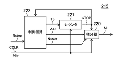
- FIG. 3 shows a detailed configuration example of the frequency divider control circuit 215 in FIG.
- the frequency divider control circuit 215 in FIG. 3 includes an integrator 220, a counter 221, and a control circuit 222.
- the control circuit 222 receives the frequency division ratio interval Nstep between the frequency sequences and sends two signals specifying the initial value Nstart of the frequency division ratio and the increment ⁇ N of the frequency division ratio per clock to the integrator 220.
- a signal designating the length Tc of one sequence of the frequency sequence, which is the time when the increment ⁇ N is to be adopted, is supplied to the counter 221.
- the integrator 220 adds the increment ⁇ N for each clock of the frequency-divided frequency signal CCLK, so that the dividing ratio changes by the increment ⁇ N over time from the initial value Nstart.
- a frequency divider control signal designating N is output.
- the increment ⁇ N is a positive value
- the frequency division ratio N increases with time.
- the increment ⁇ N is a negative value
- the frequency division ratio N decreases with time. If the increment ⁇ N is 0, The frequency division ratio N maintains a constant value.
- the counter 221 counts the number of clocks of the divided frequency signal CCLK, and outputs a count end signal STOP when the count reaches the count corresponding to the set time Tc, that is, when the time Tc has elapsed.
- the control circuit 222 updates the three outputs Nstart, ⁇ N, and Tc.
- the integrator 220 starts the next operation with the updated Nstart and ⁇ N.
- FIG. 4 is a graph showing an ideal change over time of the output frequency fvco of the frequency sweep circuit 150.
- the period from time t1 to time tx + Tc is an up-chirp period in which the output frequency fvco is increased substantially linearly from the first frequency f1 to the second frequency fx + ⁇ f (f1 ⁇ fx).
- the operation from time t1 to time tx + Tc is repeated.
- the frequency sweep during the up-chirp period is used for distance measurement.
- the number m of frequency sequences from time t1 to time tx + Tc is X.
- a frequency interval fstep (fstep ⁇ f) based on the dividing ratio interval Nstep is set between the frequency sequences. In other words, when the frequency sequence is switched, the frequency interval fstep is added to each frequency value by adding the frequency division ratio interval Nstep to each of the frequency division ratios N in the next frequency sequence.
- Tc1 Tc2
- Tc2 the length up to the switching of the output frequency fvco
- FIG. 5 is a graph showing an example of frequency division ratio control corresponding to FIG. 4 when the frequency sweep circuit 150 of FIG. 2 is used.
- the third frequency division ratio N3 is continued.
- the length from time t2 to time t5 is Tc2.
- the length from time t5 to time t8 is Tc1.
- the time change rate of the frequency division ratio N in the increase of the frequency division ratio N from the second frequency division ratio N2 to the third frequency division ratio N3 from the time t3 to the time t4 (slope of the graph) Is the time change rate of the frequency division ratio N in the increase of the frequency division ratio N from the first frequency division ratio N1 to the second frequency division ratio N2 between time t2 and time t3 (in the graph, (Slope) is controlled to be smaller than the absolute value.
- the time change rate of the frequency division ratio N in the decrease of the frequency division ratio N from the third frequency division ratio N3 to the fourth frequency division ratio N4 between the time t5 and the time t6 (in the graph, (Slope) is controlled to be smaller than the absolute value.
- FIG. 7 is a graph showing an example of a real-time change of the output frequency fvco in the case of the frequency division ratio control of FIG.
- the absolute value of the time change rate of the frequency division ratio N at the time of increase from the first frequency division ratio N1 to the second frequency division ratio N2 is large.
- Overshoot occurs in the output frequency fvco at the timing of switching from the division ratio N1 of 1 to the second division ratio N2.
- the fluctuation of the output frequency fvco due to the overshoot can be reduced to a predetermined frequency bandwidth (for example, from the first frequency f1 to the third frequency f3). ). Further, the time required for the frequency to stabilize at the time of frequency transition can be reduced.
- the third frequency division is performed.
- An undershoot occurs in the output frequency fvco at the timing of switching from the ratio N3 to the fourth frequency dividing ratio N4.
- the fourth frequency division ratio N4 in anticipation of this transient phenomenon, the fluctuation of the output frequency fvco due to undershoot can be reduced to a predetermined frequency bandwidth (for example, from the third frequency f3 to the first frequency f11). ). Further, the time required for the frequency to stabilize at the time of frequency transition can be reduced.
- the present invention is not limited to this, and may be increased in three or more stages.
- FIG. 8 shows an example in which the frequency division ratio is increased in six stages between time t2 and time t5.
- the absolute value of the time rate of change of the frequency division ratio N is increased each time the frequency increases in the phase where the frequency division ratio N is increased, and every time the level decreases in the phase where the frequency division ratio is decreased. The value is getting smaller. As a result, the amount of overshoot / the amount of undershoot can be further reduced.
- the frequency interval ⁇ f of the output frequency signal OUT in the frequency sequence of the output frequency signal OUT is plus ( ⁇ f> 0).
- the frequency interval ⁇ f of the frequency signal OUT may be minus ( ⁇ f ⁇ 0).
- two output frequency signals OUT having a frequency interval ⁇ f of ⁇ f ( ⁇ f> 0) are output in each frequency series.
- the present invention is not limited to this, and three or more output frequency signals OUT are output.
- the frequency signal OUT may be output.
- FIG. 10 shows an example in which the frequency sweep circuit 150 outputs three output frequency signals OUT having a negative frequency interval ⁇ f ( ⁇ f ⁇ 0) in each frequency series.
- the frequency interval ⁇ f2 ( ⁇ f2 ⁇ 0) between the second output frequency signal OUT (length: Tc2) and the third output frequency signal OUT (length Tc3) may be equal to or different from each other. May be.
- the operation (up-chirp period) from time t1 to time tx + Tc is repeated in frequency sweeping circuit 150, but the present invention is not limited to this.
- the frequency sweeping circuit 150 determines that the output frequency fvco is approximately from the first frequency f1 to the second frequency fx ⁇ f (f1> fx, ⁇ f> 0) within a predetermined period. It may have a characteristic of a down-chirp that decreases linearly, and the down-chirp period may be repeated.
- FIG. 11 is a circuit block diagram of a radar device according to the second embodiment of the present disclosure.
- the radar device in FIG. 11 includes two transmission system circuits 100a and 100b each having the configuration of the transmission system 100 in FIG. 1, and two reception system circuits 120a and 120b each having the configuration of the reception system 120 in FIG. , A frequency sweep circuit 150 that outputs a local oscillation signal, and a DSP 160 that controls the entire radar apparatus.
- the configuration of the frequency sweep circuit 150 can be applied to the same configuration as that shown in FIGS. 2 and 3, and the same effect can be obtained.
- the frequency sweep circuit according to the present invention has an effect of mitigating the adverse effect of the transient fluctuation occurring in the output frequency, and is useful as a frequency sweep circuit or the like for a distance measurement sensor.
- Frequency sweep circuit 210 Input terminal 211 Phase comparator 213 Voltage controlled oscillator (VCO) 214 frequency divider 215 frequency divider control circuit 216 output terminal
- VCO Voltage controlled oscillator
Landscapes
- Engineering & Computer Science (AREA)
- Radar, Positioning & Navigation (AREA)
- Remote Sensing (AREA)
- Computer Networks & Wireless Communication (AREA)
- Physics & Mathematics (AREA)
- General Physics & Mathematics (AREA)
- Radar Systems Or Details Thereof (AREA)
Abstract
A frequency divider control circuit (215) outputs a frequency division control signal such that a frequency division ratio is caused to increase from a first frequency division ratio through a second frequency division ratio greater than the first frequency division ratio to a third frequency division ratio greater than the second frequency division ratio, and then the frequency division ratio is returned from the third frequency division ratio through a fourth frequency division ratio smaller than the third frequency division ratio to a fifth frequency division ratio that is smaller than the fourth frequency division ratio and greater than the first frequency division ratio. Moreover, a control is performed so that the absolute value of a time change rate of the frequency division ratio during the increase from the second frequency division ratio to the third frequency division ratio is less than the absolute value of a time change rate of the frequency division ratio during the increase from the first frequency division ratio to the second frequency division ratio.
Description
本発明は、周波数掃引回路およびそれを用いたレーダー装置に関するものである。
The present invention relates to a frequency sweep circuit and a radar device using the same.
マイクロ波やミリ波を用いて距離計測等を行う各種レーダーセンサーでは、FMCW(Frequency Modulated Continuous Wave)方式やFMSK(Frequency Modulated Shift Keying)方式、パルス変調方式等が採用されている。
Various radar sensors that perform distance measurement and the like using microwaves and millimeter waves employ an FMCW (Frequency Modulated Continuous Wave) method, an FMSK (Frequency Modulated Shift Shift Keying) method, a pulse modulation method, and the like.
例えば、特許文献1では、レーダー装置において、距離および速度の測定の精度向上のために、互いに周波数間隔を持ち、かつそれぞれが周波数ステップを持って段階的に出力周波数が変更された送信波を用いることが開示されている。
For example, in Patent Literature 1, in a radar device, a transmission wave having a frequency interval from each other and each having a frequency step and having an output frequency changed stepwise is used in order to improve the accuracy of distance and speed measurement. It is disclosed.
一般的に、上記のような送信波を生成するために、周波数掃引回路には、電圧制御発振器(VCO)を備えたPLL(Phase Locked Loop)回路が用いられている。この回路構成には、出力周波数の切り替えのたびに送信波にオーバーシュート/アンダーシュートが発生する課題があり、特に、互いに周波数間隔を持った送信波において顕著である。
Generally, a PLL (Phase Locked Loop) circuit provided with a voltage controlled oscillator (VCO) is used for the frequency sweep circuit to generate the transmission wave as described above. This circuit configuration has a problem that overshoot / undershoot occurs in the transmission wave every time the output frequency is switched, and is particularly remarkable in transmission waves having a frequency interval from each other.
このように出力周波数にオーバーシュート/アンダーシュートが発生すると、そのオーバーシュート/アンダーシュートが収まるまで待つことにより、距離計測等を行うためのセンシング期間を大きくとることができず、測定値のS/N比が低下する。さらに、電波法などで規定される占有周波数帯域幅の制約を満たせない。そうかと言ってブランク期間を延長すれば、レーダーセンサーの距離や速度の計測精度が粗くなる。
When an overshoot / undershoot occurs in the output frequency in this way, by waiting until the overshoot / undershoot stops, a sensing period for performing distance measurement or the like cannot be extended, and the S / S The N ratio decreases. Furthermore, it cannot satisfy the restrictions on the occupied frequency bandwidth specified by the Radio Law and the like. On the other hand, if the blanking period is extended, the accuracy of measuring the distance and speed of the radar sensor is reduced.
本発明は、上記課題を解決することを目的とするものである。
The present invention aims to solve the above problems.
上記目的を達成するため、本発明の第1の観点によれば、互いに周波数間隔を有する複数の発振信号を出力する周波数掃引回路であって、基準周波数信号が入力される入力端子と、出力周波数信号に接続された出力端子と、位相比較信号に基づき前記出力周波数信号を出力する電圧制御発振器と、分周器制御信号を出力する分周器制御回路と、前記出力周波数信号が入力され、前記分周器制御信号で指定される分周比で前記出力周波数信号を分周して分周周波数信号を出力する分周器と、前記基準周波数信号と前記分周周波数信号との位相を比較し、前記位相比較信号を出力する位相比較器とを備え、前記分周器制御回路は、前記分周比を第1の分周比から、前記第1の分周比よりも大きい第2の分周比を介して、前記第2の分周比よりも大きい第3の分周比に増加させた上で、前記第3の分周比よりも小さい第4の分周比を介して、前記第4の分周比よりも小さくかつ前記第1の分周比よりも大きい第5の分周比に戻すような前記分周器制御信号を出力し、前記第2の分周比から前記第3の分周比への前記分周比の増加における前記分周比の時間変化率の絶対値は、前記第1の分周比から前記第2の分周比への前記分周比の増加における前記分周比の時間変化率の絶対値よりも小さくなるように制御される。
To achieve the above object, according to a first aspect of the present invention, there is provided a frequency sweep circuit for outputting a plurality of oscillation signals having a frequency interval from each other, comprising: an input terminal to which a reference frequency signal is input; An output terminal connected to the signal, a voltage-controlled oscillator that outputs the output frequency signal based on a phase comparison signal, a frequency divider control circuit that outputs a frequency divider control signal, and the output frequency signal is input, A frequency divider that divides the output frequency signal at a frequency division ratio specified by a frequency divider control signal and outputs a frequency-divided frequency signal, and compares the phases of the reference frequency signal and the frequency-divided frequency signal. And a phase comparator that outputs the phase comparison signal, wherein the frequency divider control circuit increases the frequency division ratio from the first frequency division ratio to a second frequency divider that is larger than the first frequency division ratio. Via the circumference ratio, more than the second frequency division ratio After increasing to a third frequency division ratio, the fourth frequency division ratio is smaller than the fourth frequency division ratio and the first frequency division ratio via a fourth frequency division ratio smaller than the third frequency division ratio. Outputting the frequency divider control signal to return the frequency to a fifth frequency division ratio larger than the frequency division ratio, and increasing the frequency division ratio from the second frequency division ratio to the third frequency division ratio. The absolute value of the time change rate of the frequency division ratio is smaller than the absolute value of the time change rate of the frequency division ratio when the frequency division ratio increases from the first frequency division ratio to the second frequency division ratio. Is controlled so that
上記第1の観点によれば、第1の分周比から第2の分周比への分周比の増加区間と、第2の分周比から第3の分周比への分周比の増加区間とを比較すると、後者の区間の方が、分周比の時間変化率の絶対値が小さいので、過渡変動が生じにくい。
According to the first aspect, the frequency division ratio increasing section from the first frequency division ratio to the second frequency division ratio, and the frequency division ratio from the second frequency division ratio to the third frequency division ratio Compared with the increase section, the latter section has a smaller absolute value of the time rate of change of the frequency division ratio, so that transient fluctuation is less likely to occur.
また、本発明の第2の観点によれば、互いに周波数間隔が設定された複数の発振信号を出力する周波数掃引回路であって、基準周波数信号が入力される入力端子と、出力周波数信号に接続された出力端子と、位相比較信号に基づき前記出力周波数信号を出力する電圧制御発振器と、分周器制御信号を出力する分周器制御回路と、前記出力周波数信号が入力され、前記分周器制御信号で指定される分周比で前記出力周波数信号を分周して分周周波数信号を出力する分周器と、前記基準周波数信号と前記分周周波数信号との位相を比較し、前記位相比較信号を出力する位相比較器とを備え、前記分周器制御回路は、前記分周比を第1の分周比から、前記第1の分周比よりも小さい第2の分周比を介して、前記第2の分周比よりも小さい第3の分周比に減少させた上で、前記第3の分周比よりも大きい第4の分周比を介して、前記第4の分周比よりも大きくかつ前記第1の分周比よりも小さい第5の分周比に戻すような前記分周器制御信号を出力し、前記第2の分周比から前記第3の分周比への前記分周比の減少における前記分周比の時間変化率の絶対値は、前記第1の分周比から前記第2の分周比への前記分周比の減少における前記分周比の時間変化率の絶対値よりも小さくなるように制御される。
According to a second aspect of the present invention, there is provided a frequency sweeping circuit for outputting a plurality of oscillation signals having frequency intervals set to each other, wherein the frequency sweeping circuit is connected to an input terminal to which a reference frequency signal is input and to an output frequency signal. Output terminal, a voltage controlled oscillator that outputs the output frequency signal based on a phase comparison signal, a frequency divider control circuit that outputs a frequency divider control signal, and the frequency divider that receives the output frequency signal, A frequency divider that divides the output frequency signal by a frequency division ratio specified by a control signal and outputs a frequency-divided frequency signal, and compares the phases of the reference frequency signal and the frequency-divided frequency signal, A phase comparator that outputs a comparison signal, wherein the frequency divider control circuit sets the frequency division ratio from a first frequency division ratio to a second frequency division ratio smaller than the first frequency division ratio. A third frequency division ratio smaller than the second frequency division ratio And then, through a fourth frequency division ratio larger than the third frequency division ratio, a fourth frequency division ratio larger than the fourth frequency division ratio and smaller than the first frequency division ratio. The frequency divider control signal is output so as to return to the frequency division ratio of 5, and the time change of the frequency division ratio in decreasing the frequency division ratio from the second frequency division ratio to the third frequency division ratio The absolute value of the rate is controlled to be smaller than the absolute value of the time rate of change of the frequency division ratio when the frequency division ratio decreases from the first frequency division ratio to the second frequency division ratio. .
上記第2の観点によれば、第1の分周比から第2の分周比への分周比の減少区間と、第2の分周比から第3の分周比への分周比の減少区間とを比較すると、後者の区間の方が、分周比の時間変化率の絶対値が小さいので、過渡変動が生じにくい。
According to the second aspect, the division interval of the division ratio from the first division ratio to the second division ratio, and the division ratio from the second division ratio to the third division ratio When compared with the decreasing section, the latter section has a smaller absolute value of the time rate of change of the frequency division ratio, so that transient fluctuation is less likely to occur.
本発明によれば、周波数掃引回路の出力周波数に生じる過渡変動の悪影響を緩和することができる。
According to the present invention, it is possible to mitigate the adverse effects of transient fluctuations occurring in the output frequency of the frequency sweep circuit.
以下、本開示の実施形態を図面に基づいて詳細に説明する。
Hereinafter, embodiments of the present disclosure will be described in detail with reference to the drawings.
<第1の実施形態>
図1は、第1の実施形態に係るレーダー装置の回路ブロック図である。図1のレーダー装置は、送信系100と、受信系120と、局部発振信号を出力する周波数掃引回路150と、レーダー装置全体の制御を司るデジタルシグナルプロセッサ(DSP)160とを備える。 <First embodiment>
FIG. 1 is a circuit block diagram of the radar device according to the first embodiment. 1 includes atransmission system 100, a reception system 120, a frequency sweep circuit 150 that outputs a local oscillation signal, and a digital signal processor (DSP) 160 that controls the entire radar device.
図1は、第1の実施形態に係るレーダー装置の回路ブロック図である。図1のレーダー装置は、送信系100と、受信系120と、局部発振信号を出力する周波数掃引回路150と、レーダー装置全体の制御を司るデジタルシグナルプロセッサ(DSP)160とを備える。 <First embodiment>
FIG. 1 is a circuit block diagram of the radar device according to the first embodiment. 1 includes a
送信系100は、周波数掃引回路150から局部発振信号を受ける送信用入力110と、送信用入力110を介して受けた局部発振信号を増幅して送信信号を生成する電力増幅器(PA)101と、目標物へ向けて送信信号を電磁波として送出する送信アンテナ102とを有する。
The transmission system 100 includes a transmission input 110 that receives a local oscillation signal from the frequency sweep circuit 150, a power amplifier (PA) 101 that amplifies the local oscillation signal received via the transmission input 110 to generate a transmission signal, A transmission antenna 102 for transmitting a transmission signal as an electromagnetic wave toward a target.
受信系120は、送信用入力110とは別に周波数掃引回路150から局部発振信号を受ける受信用入力140と、送信信号に基づく目標物からの反射波を受信する受信アンテナ121とに加えて、低雑音増幅器(LNA)123、IQ生成回路124と、ミキサ(MIXI,MIXQ)126,127と、アナログデジタル変換(ADC)回路134とを有する。
The receiving system 120 includes a receiving input 140 that receives a local oscillation signal from the frequency sweep circuit 150 separately from the transmitting input 110, and a receiving antenna 121 that receives a reflected wave from a target based on the transmitting signal. It has a noise amplifier (LNA) 123, an IQ generation circuit 124, mixers (MIXI, MIXQ) 126 and 127, and an analog-to-digital conversion (ADC) circuit 134.
また、ミキサ126,127とADC回路134との間のIFI信号及びIFQ信号の経路には、IF増幅器130,131と、フィルタ132,133とが設けられている。
{Circle around (1)} In the paths of the IFI signal and the IFQ signal between the mixers 126 and 127 and the ADC circuit 134, IF amplifiers 130 and 131 and filters 132 and 133 are provided.
図2は、図1中の周波数掃引回路150の構成を示している。図2の周波数掃引回路150は、入力端子210と、位相比較器211と、ループフィルタ212と、電圧制御発振器(VCO)213と、分周器214と、分周器制御回路215と、出力端子216とを備えている。入力端子210には、一定の基準周波数frefを有する基準周波数信号RCLKが入力される。基準周波数信号RCLKは、例えば水晶発振器から供給を受けることができる。出力端子216は、可変の出力周波数fvcoを有する出力周波数信号OUTに接続されている。電圧制御発振器213は、位相比較器211からループフィルタ212を経由して供給された位相比較信号に基づき、発振信号としての出力周波数信号OUTを出力する。出力周波数信号OUTは、局部発振信号として送信用入力110および受信用入力140に与えられる。分周器制御回路215は、分周比Nを指定する分周器制御信号を出力する。分周器214は、出力周波数信号OUTが入力され、分周器制御信号で指定された分周比Nで出力周波数信号OUTを分周して、分周周波数fdivを有する分周周波数信号CCLKを出力する。位相比較器211は、基準周波数信号RCLKと分周周波数信号CCLKとの位相を比較し、位相比較信号を出力する。分周器制御回路215は、タイミング制御のために分周器214から分周周波数信号CCLKの入力を受ける。ただし、分周器制御回路215は、分周周波数信号CCLKに代えて基準周波数信号RCLKを入力してもよい。
FIG. 2 shows the configuration of the frequency sweep circuit 150 in FIG. 2 includes an input terminal 210, a phase comparator 211, a loop filter 212, a voltage controlled oscillator (VCO) 213, a frequency divider 214, a frequency divider control circuit 215, and an output terminal. 216. The input terminal 210 receives a reference frequency signal RCLK having a constant reference frequency fref. The reference frequency signal RCLK can be supplied from, for example, a crystal oscillator. The output terminal 216 is connected to an output frequency signal OUT having a variable output frequency fvco. The voltage controlled oscillator 213 outputs an output frequency signal OUT as an oscillation signal based on the phase comparison signal supplied from the phase comparator 211 via the loop filter 212. The output frequency signal OUT is provided to the input 110 for transmission and the input 140 for reception as a local oscillation signal. The frequency divider control circuit 215 outputs a frequency divider control signal designating the frequency division ratio N. The frequency divider 214 receives the output frequency signal OUT, divides the frequency of the output frequency signal OUT by the frequency division ratio N specified by the frequency divider control signal, and generates a frequency-divided frequency signal CCLK having the frequency division frequency fdiv. Output. The phase comparator 211 compares the phases of the reference frequency signal RCLK and the divided frequency signal CCLK, and outputs a phase comparison signal. The frequency divider control circuit 215 receives the frequency-divided frequency signal CCLK from the frequency divider 214 for timing control. However, the divider control circuit 215 may input the reference frequency signal RCLK instead of the divided frequency signal CCLK.
図1の周波数掃引回路150によれば、fvco=fref×Nとなり、分周比Nに比例して出力周波数fvcoが変化する。
According to the frequency sweep circuit 150 in FIG. 1, fvco = fref × N, and the output frequency fvco changes in proportion to the frequency division ratio N.
図3は、図2中の分周器制御回路215の詳細構成例を示している。図3の分周器制御回路215は、積分器220と、カウンタ221と、制御回路222とを備えている。制御回路222は、周波数系列間の分周比間隔Nstepを受け、分周比の初期値Nstartと、1クロック当たりの分周比の増分ΔNとを指定する2つの信号を積分器220へ、当該増分ΔNを採用すべき時間である周波数系列の1系列の長さTcを指定する信号をカウンタ221へそれぞれ供給する。
FIG. 3 shows a detailed configuration example of the frequency divider control circuit 215 in FIG. The frequency divider control circuit 215 in FIG. 3 includes an integrator 220, a counter 221, and a control circuit 222. The control circuit 222 receives the frequency division ratio interval Nstep between the frequency sequences and sends two signals specifying the initial value Nstart of the frequency division ratio and the increment ΔN of the frequency division ratio per clock to the integrator 220. A signal designating the length Tc of one sequence of the frequency sequence, which is the time when the increment ΔN is to be adopted, is supplied to the counter 221.
積分器220は、初期値Nstartが設定された後、分周周波数信号CCLKの1クロック毎に増分ΔNを加算していくことで、初期値Nstartから時間の経過とともに増分ΔNずつ変化する分周比Nを指定する分周器制御信号を出力する。ここで、増分ΔNが正の値であれば分周比Nが時間経過とともに増加し、増分ΔNが負の値であれば分周比Nが時間経過とともに減少し、増分ΔNが0であれば分周比Nが一定値を保持することになる。
After the initial value Nstart is set, the integrator 220 adds the increment ΔN for each clock of the frequency-divided frequency signal CCLK, so that the dividing ratio changes by the increment ΔN over time from the initial value Nstart. A frequency divider control signal designating N is output. Here, if the increment ΔN is a positive value, the frequency division ratio N increases with time. If the increment ΔN is a negative value, the frequency division ratio N decreases with time. If the increment ΔN is 0, The frequency division ratio N maintains a constant value.
一方、カウンタ221は、分周周波数信号CCLKのクロック数をカウントし、設定された時間Tcに相当するカウント数になれば、すなわち時間Tcが経過した時点でカウント終了信号STOPを出力する。制御回路222は、カウント終了信号STOPを受けると、3つの出力Nstart,ΔN,Tcを更新する。積分器220は、カウント終了信号STOPを受けると、更新されたNstart,ΔNによって次の動作を開始する。
On the other hand, the counter 221 counts the number of clocks of the divided frequency signal CCLK, and outputs a count end signal STOP when the count reaches the count corresponding to the set time Tc, that is, when the time Tc has elapsed. Upon receiving the count end signal STOP, the control circuit 222 updates the three outputs Nstart, ΔN, and Tc. Upon receiving the count end signal STOP, the integrator 220 starts the next operation with the updated Nstart and ΔN.
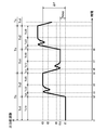
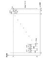
図4は、周波数掃引回路150の出力周波数fvcoの理想的経時変化を示すグラフである。図4によれば、時刻t1から時刻tx+Tcまでが、出力周波数fvcoを第1の周波数f1から第2の周波数fx+Δf(f1<fx)まで略直線的に上げるアップチャープ期間である。周波数掃引回路150では、この時刻t1から時刻tx+Tcまでの動作が繰り返される。そして、このアップチャープ期間の周波数掃引が距離計測に利用される。
FIG. 4 is a graph showing an ideal change over time of the output frequency fvco of the frequency sweep circuit 150. According to FIG. 4, the period from time t1 to time tx + Tc is an up-chirp period in which the output frequency fvco is increased substantially linearly from the first frequency f1 to the second frequency fx + Δf (f1 <fx). In frequency sweep circuit 150, the operation from time t1 to time tx + Tc is repeated. The frequency sweep during the up-chirp period is used for distance measurement.
図4では、時刻t1から時刻tx+Tcまでの間における周波数系列数mがXである、換言すると、図4では、Tcの期間がX回にわたって繰り返される(tx+Tc-t1=Tc×X)。周波数掃引回路150は、各周波数系列において、互いにΔf(Δf>0)の周波数間隔を有する2つの出力周波数信号OUT(出力周波数=fvco)を出力する。そして、周波数系列間には、分周比間隔Nstepに基づく周波数間隔fstep(fstep<Δf)が設定されている。換言すると、周波数系列が切り替わると、次の周波数系列では、各分周比Nに分周比間隔Nstepが加算されることで、各周波数値に周波数間隔fstepが加算され、それが(X-1)回繰り返される(図6参照)。ここで、Tcのうち、出力周波数fvcoの切替までの長さをTc1といい、同切替後の長さをTc2という。なお、図4では、Tc1=Tc2の例を示しているが、Tc1とTc2の長さが互いに異なっていてもよい。
で は In FIG. 4, the number m of frequency sequences from time t1 to time tx + Tc is X. In other words, in FIG. 4, the period of Tc is repeated X times (tx + Tc−t1 = Tc × X). The frequency sweep circuit 150 outputs two output frequency signals OUT (output frequency = fvco) having a frequency interval of Δf (Δf> 0) in each frequency series. A frequency interval fstep (fstep <Δf) based on the dividing ratio interval Nstep is set between the frequency sequences. In other words, when the frequency sequence is switched, the frequency interval fstep is added to each frequency value by adding the frequency division ratio interval Nstep to each of the frequency division ratios N in the next frequency sequence. ) Times (see FIG. 6). Here, of the Tc, the length up to the switching of the output frequency fvco is called Tc1, and the length after the switching is called Tc2. Although FIG. 4 shows an example in which Tc1 = Tc2, the lengths of Tc1 and Tc2 may be different from each other.
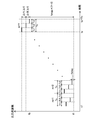
図5は、図2の周波数掃引回路150を用いた場合の図4に対応した分周比制御の例を示すグラフである。
FIG. 5 is a graph showing an example of frequency division ratio control corresponding to FIG. 4 when the frequency sweep circuit 150 of FIG. 2 is used.
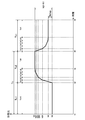
図5に示すように、時刻t1から時刻t2までの間(長さ:Tc1)、第1の分周比N1(=f1/fref)が継続される。
As shown in FIG. 5, the first frequency division ratio N1 (= f1 / fref) is continued from time t1 to time t2 (length: Tc1).
その後、時刻t2から時刻t3までで(長さ:Tc21)、第1の分周比N1から第2の分周比N2(=f2/fref)へ直線的に増加させられる(N1<N2)。さらに、時刻t3から時刻t4までで(長さ:Tc22)、第2の分周比N2から第3の分周比N3(=f3/fref)へ直線的に増加させられ(N2<N3)、時刻t4から時刻t5までの間(長さ:T23)、第3の分周比N3が継続される。ここで、時刻t2から時刻t5までの長さがTc2である。
Thereafter, from time t2 to time t3 (length: Tc21), the frequency is linearly increased from the first frequency dividing ratio N1 to the second frequency dividing ratio N2 (= f2 / fref) (N1 <N2). Further, from time t3 to time t4 (length: Tc22), the frequency is linearly increased from the second frequency dividing ratio N2 to the third frequency dividing ratio N3 (= f3 / fref) (N2 <N3), From time t4 to time t5 (length: T23), the third frequency division ratio N3 is continued. Here, the length from time t2 to time t5 is Tc2.
次に、時刻t5から時刻t6までで(長さ:Tc11)、第3の分周比N3から第4の分周比N4(=f4/fref)へ直線的に減少させられる(N3>N4)。さらに、時刻t6から時刻t7までで(長さ:Tc12)、第4の分周比N4から次の周波数系列における第1の分周比N11(=f11/fref=f1/fref+Nstep)へ直線的に減少させられ(N4>N11)、時刻t7から時刻t8までの間(長さ:T13)、第1の分周比N11が継続される。ここで、時刻t5から時刻t8までの長さがTc1である。
Next, from the time t5 to the time t6 (length: Tc11), the third frequency dividing ratio N3 is linearly decreased from the third frequency dividing ratio N4 to the fourth frequency dividing ratio N4 (= f4 / fref) (N3> N4). . Further, from time t6 to time t7 (length: Tc12), the fourth frequency division ratio N4 is linearly changed to the first frequency division ratio N11 (= f11 / fref = f1 / fref + Nstep) in the next frequency series. It is decreased (N4> N11), and the first frequency division ratio N11 is continued from time t7 to time t8 (length: T13). Here, the length from time t5 to time t8 is Tc1.
それ以降、時刻t2から時刻t8までの動作が繰り返される。このとき、繰り返しのたびに、分周比間隔Nstepが加算されるようになっている(図6の時刻t8から時刻t9を参照)。
以降 Thereafter, the operation from time t2 to time t8 is repeated. At this time, the frequency division ratio interval Nstep is added every time the repetition is performed (see time t8 to time t9 in FIG. 6).
ここで、時刻t3から時刻t4までの間における、第2の分周比N2から第3の分周比N3への分周比Nの増加における分周比Nの時間変化率(グラフの傾き)の絶対値は、時刻t2から時刻t3までの間における、第1の分周比N1から第2の分周比N2への分周比Nの増加における分周比Nの時間変化率(グラフの傾き)の絶対値よりも小さくなるように制御される。
Here, the time change rate of the frequency division ratio N in the increase of the frequency division ratio N from the second frequency division ratio N2 to the third frequency division ratio N3 from the time t3 to the time t4 (slope of the graph) Is the time change rate of the frequency division ratio N in the increase of the frequency division ratio N from the first frequency division ratio N1 to the second frequency division ratio N2 between time t2 and time t3 (in the graph, (Slope) is controlled to be smaller than the absolute value.
同様に、時刻t6から時刻t7までの間における、第4の分周比N4から第1の分周比N11への分周比Nの減少における分周比Nの時間変化率(グラフの傾き)の絶対値は、時刻t5から時刻t6までの間における、第3の分周比N3から第4の分周比N4への分周比Nの減少における分周比Nの時間変化率(グラフの傾き)の絶対値よりも小さくなるように制御される。
Similarly, the rate of time change (gradient of the graph) of the frequency division ratio N in the decrease of the frequency division ratio N from the fourth frequency division ratio N4 to the first frequency division ratio N11 from the time t6 to the time t7. Is the time change rate of the frequency division ratio N in the decrease of the frequency division ratio N from the third frequency division ratio N3 to the fourth frequency division ratio N4 between the time t5 and the time t6 (in the graph, (Slope) is controlled to be smaller than the absolute value.
図7は、図5の分周比制御の場合の出力周波数fvcoの実経時変化の例を示すグラフである。
FIG. 7 is a graph showing an example of a real-time change of the output frequency fvco in the case of the frequency division ratio control of FIG.
図7に示すように、第1の分周比N1から第2の分周比N2への増加時(時刻t2から時刻t3)における分周比Nの時間変化率の絶対値が大きいので、第1の分周比N1から第2の分周比N2への切り替わりのタイミングにて出力周波数fvcoにオーバーシュートが発生する。しかしながら、この過渡現象を見越して第2の分周比N2を設定することにより、オーバーシュートによる出力周波数fvcoの変動を所定の周波数帯域幅(例えば、第1の周波数f1から第3の周波数f3まで)の中に収めることが可能である。さらに、周波数遷移時に周波数が安定するまでの時間を短縮することができる。
As shown in FIG. 7, the absolute value of the time change rate of the frequency division ratio N at the time of increase from the first frequency division ratio N1 to the second frequency division ratio N2 (from time t2 to time t3) is large. Overshoot occurs in the output frequency fvco at the timing of switching from the division ratio N1 of 1 to the second division ratio N2. However, by setting the second frequency division ratio N2 in anticipation of this transient phenomenon, the fluctuation of the output frequency fvco due to the overshoot can be reduced to a predetermined frequency bandwidth (for example, from the first frequency f1 to the third frequency f3). ). Further, the time required for the frequency to stabilize at the time of frequency transition can be reduced.
同様に、第3の分周比N3から第4の分周比N4への減少時(時刻t5から時刻t6)における分周比Nの時間変化率の絶対値が大きいので、第3の分周比N3から第4の分周比N4への切り替わりのタイミングにて出力周波数fvcoにアンダーシュートが発生する。しかしながら、この過渡現象を見越して第4の分周比N4を設定することにより、アンダーシュートによる出力周波数fvcoの変動を所定の周波数帯域幅(例えば、第3の周波数f3から第1の周波数f11まで)の中に収めることが可能である。さらに、周波数遷移時に周波数が安定するまでの時間を短縮することができる。
Similarly, since the absolute value of the time change rate of the frequency division ratio N at the time of the decrease from the third frequency division ratio N3 to the fourth frequency division ratio N4 (from time t5 to time t6) is large, the third frequency division is performed. An undershoot occurs in the output frequency fvco at the timing of switching from the ratio N3 to the fourth frequency dividing ratio N4. However, by setting the fourth frequency division ratio N4 in anticipation of this transient phenomenon, the fluctuation of the output frequency fvco due to undershoot can be reduced to a predetermined frequency bandwidth (for example, from the third frequency f3 to the first frequency f11). ). Further, the time required for the frequency to stabilize at the time of frequency transition can be reduced.
-変形例-
上記実施形態の構成は、以下のようにしてもよい。なお、その場合においても、具体的な動作およびその効果は、上記実施形態と同様であり、ここではその詳細説明を省略する。 -Variation-
The configuration of the above embodiment may be as follows. In this case, the specific operation and its effects are the same as those of the above-described embodiment, and the detailed description is omitted here.
例えば、上記実施形態では、時刻t2から時刻t4において、第1の分周比N1から第2の分周比N2および第2の分周比N2から第3の分周比N3への2段階でそれぞれ直線的に増加させられるものとしたが、これに限定されず、3段階以上で増加させることにしてもよい。
For example, in the above-described embodiment, from time t2 to time t4, there are two stages from the first frequency division ratio N1 to the second frequency division ratio N2 and the second frequency division ratio N2 to the third frequency division ratio N3. Although each is linearly increased, the present invention is not limited to this, and may be increased in three or more stages.
図8では、時刻t2から時刻t5の間において分周比を6段階で増加させた例を示している。図8によれば、分周比Nを増加させる局面では段階が上がるごとに、分周比を減少させる局面では段階が下がるごとに、分周比Nの時間変化率(グラフの傾き)の絶対値が小さくなっている。これにより、オーバーシュート量/アンダーシュート量をさらに減らすことができる。
FIG. 8 shows an example in which the frequency division ratio is increased in six stages between time t2 and time t5. According to FIG. 8, the absolute value of the time rate of change of the frequency division ratio N (slope of the graph) is increased each time the frequency increases in the phase where the frequency division ratio N is increased, and every time the level decreases in the phase where the frequency division ratio is decreased. The value is getting smaller. As a result, the amount of overshoot / the amount of undershoot can be further reduced.
また、上記実施形態では、出力周波数信号OUTの周波数系列内における出力周波数信号OUTの周波数間隔Δfがプラス(Δf>0)であるものとしたが、図9に示すように、周波数系列内における出力周波数信号OUTの周波数間隔Δfがマイナス(Δf<0)であってもよい。
Further, in the above embodiment, the frequency interval Δf of the output frequency signal OUT in the frequency sequence of the output frequency signal OUT is plus (Δf> 0). However, as shown in FIG. The frequency interval Δf of the frequency signal OUT may be minus (Δf <0).
また、上記実施形態では、各周波数系列において、互いにΔf(Δf>0)の周波数間隔Δfを有する2つの出力周波数信号OUTを出力するものとしたが、これに限定されず、3つ以上の出力周波数信号OUTを出力するようにしてもよい。
In the above embodiment, two output frequency signals OUT having a frequency interval Δf of Δf (Δf> 0) are output in each frequency series. However, the present invention is not limited to this, and three or more output frequency signals OUT are output. The frequency signal OUT may be output.
図10では、周波数掃引回路150が、各周波数系列において、マイナスの周波数間隔Δf(Δf<0)を有する3つの出力周波数信号OUTを出力する例を示している。図10に示すように、周波数系列内における、1つ目の出力周波数信号OUT(長さ:Tc1)と2つ目の出力周波数信号OUT(長さTc2)との周波数間隔Δf1(Δf1<0)と、2つめの出力周波数信号OUT(長さ:Tc2)と3つ目の出力周波数信号OUT(長さTc3)との周波数間隔Δf2(Δf2<0)とが互いに等しくてもよいし、互いに異なっていてもよい。
FIG. 10 shows an example in which the frequency sweep circuit 150 outputs three output frequency signals OUT having a negative frequency interval Δf (Δf <0) in each frequency series. As shown in FIG. 10, the frequency interval Δf1 (Δf1 <0) between the first output frequency signal OUT (length: Tc1) and the second output frequency signal OUT (length Tc2) in the frequency sequence. And the frequency interval Δf2 (Δf2 <0) between the second output frequency signal OUT (length: Tc2) and the third output frequency signal OUT (length Tc3) may be equal to or different from each other. May be.
さらに、上記実施形態では、周波数掃引回路150において、時刻t1から時刻tx+Tcまでの動作(アップチャープ期間)が繰り返されるものとしたが、これに限定されない。具体的な図示は省略するが、例えば、周波数掃引回路150が、所定の期間内に出力周波数fvcoが第1の周波数f1から第2の周波数fx-Δf(f1>fx,Δf>0)まで略直線的に下げるダウンチャープの特性を有し、そのダウンチャープ期間が繰り返されるようにしてもよい。
{Further, in the above-described embodiment, the operation (up-chirp period) from time t1 to time tx + Tc is repeated in frequency sweeping circuit 150, but the present invention is not limited to this. Although not specifically illustrated, for example, the frequency sweeping circuit 150 determines that the output frequency fvco is approximately from the first frequency f1 to the second frequency fx−Δf (f1> fx, Δf> 0) within a predetermined period. It may have a characteristic of a down-chirp that decreases linearly, and the down-chirp period may be repeated.
<第2の実施形態>
図11は、本開示の第2の実施形態に係るレーダー装置の回路ブロック図である。図11のレーダー装置は、各々図1中の送信系100の構成を有する2つの送信系回路100a,100bと、各々図1中の受信系120の構成を有する2つの受信系回路120a,120bと、局部発振信号を出力する周波数掃引回路150と、レーダー装置全体の制御を司るDSP160とを備える。図11においても、周波数掃引回路150の構成は、図2および図3に示したものと共通の構成を適用でき、同様の効果が得られる。 <Second embodiment>
FIG. 11 is a circuit block diagram of a radar device according to the second embodiment of the present disclosure. The radar device in FIG. 11 includes two transmission system circuits 100a and 100b each having the configuration of the transmission system 100 in FIG. 1, and two reception system circuits 120a and 120b each having the configuration of the reception system 120 in FIG. , A frequency sweep circuit 150 that outputs a local oscillation signal, and a DSP 160 that controls the entire radar apparatus. In FIG. 11 as well, the configuration of the frequency sweep circuit 150 can be applied to the same configuration as that shown in FIGS. 2 and 3, and the same effect can be obtained.
図11は、本開示の第2の実施形態に係るレーダー装置の回路ブロック図である。図11のレーダー装置は、各々図1中の送信系100の構成を有する2つの送信系回路100a,100bと、各々図1中の受信系120の構成を有する2つの受信系回路120a,120bと、局部発振信号を出力する周波数掃引回路150と、レーダー装置全体の制御を司るDSP160とを備える。図11においても、周波数掃引回路150の構成は、図2および図3に示したものと共通の構成を適用でき、同様の効果が得られる。 <Second embodiment>
FIG. 11 is a circuit block diagram of a radar device according to the second embodiment of the present disclosure. The radar device in FIG. 11 includes two
以上説明してきたとおり、本発明に係る周波数掃引回路は、出力周波数に生じる過渡変動の悪影響を緩和する効果を有し、距離計測センサー用の周波数掃引回路等として有用である。
As described above, the frequency sweep circuit according to the present invention has an effect of mitigating the adverse effect of the transient fluctuation occurring in the output frequency, and is useful as a frequency sweep circuit or the like for a distance measurement sensor.
150 周波数掃引回路
210 入力端子
211 位相比較器
213 電圧制御発振器(VCO)
214 分周器
215 分周器制御回路
216 出力端子 150Frequency sweep circuit 210 Input terminal 211 Phase comparator 213 Voltage controlled oscillator (VCO)
214frequency divider 215 frequency divider control circuit 216 output terminal
210 入力端子
211 位相比較器
213 電圧制御発振器(VCO)
214 分周器
215 分周器制御回路
216 出力端子 150
214
Claims (7)
- 互いに周波数間隔を有する複数の発振信号を出力する周波数掃引回路であって、
基準周波数信号が入力される入力端子と、
出力周波数信号に接続された出力端子と、
位相比較信号に基づき前記出力周波数信号を出力する電圧制御発振器と、
分周器制御信号を出力する分周器制御回路と、
前記出力周波数信号が入力され、前記分周器制御信号で指定される分周比で前記出力周波数信号を分周して分周周波数信号を出力する分周器と、
前記基準周波数信号と前記分周周波数信号との位相を比較し、前記位相比較信号を出力する位相比較器とを備え、
前記分周器制御回路は、前記分周比を第1の分周比から、前記第1の分周比よりも大きい第2の分周比を介して、前記第2の分周比よりも大きい第3の分周比に増加させた上で、前記第3の分周比よりも小さい第4の分周比を介して、前記第4の分周比よりも小さくかつ前記第1の分周比よりも大きい第5の分周比に戻すような前記分周器制御信号を出力し、
前記第2の分周比から前記第3の分周比への前記分周比の増加における前記分周比の時間変化率の絶対値は、前記第1の分周比から前記第2の分周比への前記分周比の増加における前記分周比の時間変化率の絶対値よりも小さくなるように制御される
ことを特徴とする周波数掃引回路。 A frequency sweep circuit that outputs a plurality of oscillation signals having a frequency interval from each other,
An input terminal to which a reference frequency signal is input,
An output terminal connected to the output frequency signal;
A voltage controlled oscillator that outputs the output frequency signal based on a phase comparison signal,
A frequency divider control circuit that outputs a frequency divider control signal;
A frequency divider to which the output frequency signal is input, and a frequency divider that divides the output frequency signal at a frequency division ratio specified by the frequency divider control signal and outputs a divided frequency signal;
Comparing the phase of the reference frequency signal and the divided frequency signal, and a phase comparator that outputs the phase comparison signal,
The frequency divider control circuit sets the frequency division ratio to be greater than the second frequency division ratio from the first frequency division ratio via a second frequency division ratio that is larger than the first frequency division ratio. After increasing the third frequency division ratio to a large value, the fourth frequency division ratio is smaller than the fourth frequency division ratio via the fourth frequency division ratio smaller than the third frequency division ratio. Outputting the frequency divider control signal to return to a fifth frequency division ratio larger than the frequency ratio;
The absolute value of the time rate of change of the frequency division ratio in the increase of the frequency division ratio from the second frequency division ratio to the third frequency division ratio is calculated from the first frequency division ratio to the second frequency division ratio. A frequency sweeping circuit, wherein the frequency sweeping circuit is controlled so as to be smaller than an absolute value of a time rate of change of the frequency division ratio when the frequency division ratio is increased to a frequency ratio. - 請求項1記載の周波数掃引回路において、
前記第4の分周比から前記第5の分周比への前記分周比の減少における前記分周比の時間変化率の絶対値は、前記第3の分周比から前記第4の分周比への前記分周比の減少における前記分周比の時間変化率の絶対値よりも小さくなるように制御される
ことを特徴とする周波数掃引回路。 The frequency sweep circuit according to claim 1,
The absolute value of the time rate of change of the frequency division ratio in the decrease of the frequency division ratio from the fourth frequency division ratio to the fifth frequency division ratio is calculated from the third frequency division ratio to the fourth frequency division ratio. A frequency sweeping circuit, wherein the frequency sweeping circuit is controlled so as to be smaller than an absolute value of a time rate of change of the frequency division ratio when the frequency division ratio is reduced to a frequency ratio. - 請求項1または2に記載の周波数掃引回路において、
前記第2の分周比は、順次増加する方向の周波数間隔を有する複数の第2の分周比からなり、
前記各第2の分周比間の前記分周比の時間変化率の絶対値は、前記第3の分周比に近づくのにしたがって次第に小さくなり、かつ、前記第2の分周比の最大分周比から前記第3の分周比への増加における前記分周比の時間変化率の絶対値は、前記各第2の分周比間の前記分周比の時間変化率の絶対値よりも小さくなるように制御される
ことを特徴とする周波数掃引回路。 The frequency sweep circuit according to claim 1 or 2,
The second frequency division ratio includes a plurality of second frequency division ratios having frequency intervals in a sequentially increasing direction,
The absolute value of the time change rate of the frequency division ratio between the second frequency division ratios gradually decreases as approaching the third frequency division ratio, and the maximum value of the second frequency division ratio is increased. The absolute value of the time change rate of the frequency division ratio in the increase from the frequency division ratio to the third frequency division ratio is greater than the absolute value of the time change rate of the frequency division ratio between the second frequency division ratios. A frequency sweep circuit characterized in that the frequency sweep is controlled to be small. - 互いに周波数間隔が設定された複数の発振信号を出力する周波数掃引回路であって、
基準周波数信号が入力される入力端子と、
出力周波数信号に接続された出力端子と、
位相比較信号に基づき前記出力周波数信号を出力する電圧制御発振器と、
分周器制御信号を出力する分周器制御回路と、
前記出力周波数信号が入力され、前記分周器制御信号で指定される分周比で前記出力周波数信号を分周して分周周波数信号を出力する分周器と、
前記基準周波数信号と前記分周周波数信号との位相を比較し、前記位相比較信号を出力する位相比較器とを備え、
前記分周器制御回路は、前記分周比を第1の分周比から、前記第1の分周比よりも小さい第2の分周比を介して、前記第2の分周比よりも小さい第3の分周比に減少させた上で、前記第3の分周比よりも大きい第4の分周比を介して、前記第4の分周比よりも大きくかつ前記第1の分周比よりも小さい第5の分周比に戻すような前記分周器制御信号を出力し、
前記第2の分周比から前記第3の分周比への前記分周比の減少における前記分周比の時間変化率の絶対値は、前記第1の分周比から前記第2の分周比への前記分周比の減少における前記分周比の時間変化率の絶対値よりも小さくなるように制御される
ことを特徴とする周波数掃引回路。 A frequency sweep circuit that outputs a plurality of oscillation signals having frequency intervals set to each other,
An input terminal to which a reference frequency signal is input,
An output terminal connected to the output frequency signal;
A voltage controlled oscillator that outputs the output frequency signal based on a phase comparison signal,
A frequency divider control circuit that outputs a frequency divider control signal;
A frequency divider to which the output frequency signal is input, and a frequency divider that divides the output frequency signal at a frequency division ratio specified by the frequency divider control signal and outputs a divided frequency signal;
Comparing the phase of the reference frequency signal and the divided frequency signal, and a phase comparator that outputs the phase comparison signal,
The frequency divider control circuit sets the frequency division ratio to a value higher than the second frequency division ratio from the first frequency division ratio via a second frequency division ratio smaller than the first frequency division ratio. After reducing the third frequency division ratio to a smaller value, the fourth frequency division ratio is larger than the fourth frequency division ratio and the first frequency division ratio via a fourth frequency division ratio larger than the third frequency division ratio. Outputting the frequency divider control signal for returning to the fifth frequency division ratio smaller than the frequency ratio;
The absolute value of the time rate of change of the frequency division ratio in the decrease of the frequency division ratio from the second frequency division ratio to the third frequency division ratio is calculated from the first frequency division ratio to the second frequency division ratio. A frequency sweeping circuit, wherein the frequency sweeping circuit is controlled so as to be smaller than an absolute value of a time rate of change of the frequency division ratio when the frequency division ratio is reduced to a frequency ratio. - 請求項4記載の周波数掃引回路において、
前記第4の分周比から前記第5の分周比への前記分周比の増加における前記分周比の時間変化率の絶対値は、前記第3の分周比から前記第4の分周比への前記分周比の増加における前記分周比の時間変化率の絶対値よりも小さくなるように制御される
ことを特徴とする周波数掃引回路。 The frequency sweep circuit according to claim 4,
The absolute value of the time rate of change of the frequency division ratio in the increase of the frequency division ratio from the fourth frequency division ratio to the fifth frequency division ratio is calculated from the third frequency division ratio to the fourth frequency division ratio. A frequency sweeping circuit, wherein the frequency sweeping circuit is controlled so as to be smaller than an absolute value of a time rate of change of the frequency division ratio when the frequency division ratio is increased to a frequency ratio. - 請求項4または5に記載の周波数掃引回路において、
前記第2の分周比は、順次減少する方向の周波数間隔を有する複数の第2の分周比からなり、
前記各第2の分周比間の前記分周比の時間変化率の絶対値は、前記第3の分周比に近づくのにしたがって次第に小さくなり、かつ、前記第2の分周比の最大分周比から前記第3の分周比への減少における前記分周比の時間変化率の絶対値は、前記各第2の分周比間の前記分周比の時間変化率の絶対値よりも小さくなるように制御される
ことを特徴とする周波数掃引回路。 The frequency sweep circuit according to claim 4 or 5,
The second frequency division ratio includes a plurality of second frequency division ratios having frequency intervals in a sequentially decreasing direction,
The absolute value of the time change rate of the frequency division ratio between the second frequency division ratios gradually decreases as approaching the third frequency division ratio, and the maximum value of the second frequency division ratio is increased. The absolute value of the time change rate of the frequency division ratio in the decrease from the frequency division ratio to the third frequency division ratio is calculated from the absolute value of the time change rate of the frequency division ratio between the second frequency division ratios. A frequency sweep circuit characterized in that the frequency sweep is controlled to be small. - 請求項1から6のうちのいずれか1項に記載の周波数掃引回路を備えたレーダー装置。 A radar apparatus comprising the frequency sweep circuit according to any one of claims 1 to 6.
Priority Applications (3)
| Application Number | Priority Date | Filing Date | Title |
|---|---|---|---|
| PCT/JP2018/023996 WO2020003349A1 (en) | 2018-06-25 | 2018-06-25 | Frequency sweep circuit and radar device |
| JP2020526729A JPWO2020003349A1 (en) | 2018-06-25 | 2018-06-25 | Frequency sweep circuit and radar equipment |
| US17/119,639 US11846720B2 (en) | 2018-06-25 | 2020-12-11 | Frequency sweep circuit and radar device |
Applications Claiming Priority (1)
| Application Number | Priority Date | Filing Date | Title |
|---|---|---|---|
| PCT/JP2018/023996 WO2020003349A1 (en) | 2018-06-25 | 2018-06-25 | Frequency sweep circuit and radar device |
Related Child Applications (1)
| Application Number | Title | Priority Date | Filing Date |
|---|---|---|---|
| US17/119,639 Continuation US11846720B2 (en) | 2018-06-25 | 2020-12-11 | Frequency sweep circuit and radar device |
Publications (1)
| Publication Number | Publication Date |
|---|---|
| WO2020003349A1 true WO2020003349A1 (en) | 2020-01-02 |
Family
ID=68986150
Family Applications (1)
| Application Number | Title | Priority Date | Filing Date |
|---|---|---|---|
| PCT/JP2018/023996 WO2020003349A1 (en) | 2018-06-25 | 2018-06-25 | Frequency sweep circuit and radar device |
Country Status (3)
| Country | Link |
|---|---|
| US (1) | US11846720B2 (en) |
| JP (1) | JPWO2020003349A1 (en) |
| WO (1) | WO2020003349A1 (en) |
Citations (2)
| Publication number | Priority date | Publication date | Assignee | Title |
|---|---|---|---|---|
| JP2009194428A (en) * | 2008-02-12 | 2009-08-27 | Panasonic Corp | Synthesizer, receiver using the same and electronic apparatus |
| WO2017056287A1 (en) * | 2015-10-01 | 2017-04-06 | 三菱電機株式会社 | Linear chirp signal generator |
Family Cites Families (35)
| Publication number | Priority date | Publication date | Assignee | Title |
|---|---|---|---|---|
| FR2754604B1 (en) * | 1992-06-05 | 1999-04-09 | Thomson Csf | DEVICE FOR LINEARIZING A FREQUENCY MODULATION RAMP AND ITS APPLICATION TO A RADIO-ALTIMETER |
| DE19922411A1 (en) * | 1999-04-07 | 2000-10-12 | Volkswagen Ag | Radar measurement of distances, relative speeds between vehicle, obstruction(s) involves computing intercepts of all lines from 2 chirps at 2 frequency positions in distance-speed diagram |
| US6114987A (en) * | 1999-05-29 | 2000-09-05 | Sensor Technologies & Systems, Inc. | Dual-loop linearizer for FM-CW radar |
| US6577269B2 (en) * | 2000-08-16 | 2003-06-10 | Raytheon Company | Radar detection method and apparatus |
| DE10050278B4 (en) * | 2000-10-10 | 2005-06-02 | S.M.S., Smart Microwave Sensors Gmbh | Method and device for determining distance and relative speed of a remote object |
| JP3988571B2 (en) * | 2001-09-17 | 2007-10-10 | 株式会社デンソー | Radar equipment |
| DE10231597A1 (en) * | 2002-07-12 | 2004-01-29 | Robert Bosch Gmbh | Method and radar system for determining the directional angle of radar objects |
| DE102005008715A1 (en) * | 2005-02-25 | 2006-08-31 | Robert Bosch Gmbh | Radar system e.g. for motor vehicle, supplies probable collision time-point and collision speed to pre-crash-system |
| US7898344B2 (en) * | 2006-09-12 | 2011-03-01 | Fujitsu Limited | Phase-locked oscillator and multi-radar system using same |
| JP4977443B2 (en) * | 2006-10-31 | 2012-07-18 | 日立オートモティブシステムズ株式会社 | Radar apparatus and radar detection method |
| JP4871104B2 (en) * | 2006-11-24 | 2012-02-08 | 日立オートモティブシステムズ株式会社 | Radar apparatus and signal processing method |
| DE102007043535A1 (en) * | 2007-09-12 | 2009-03-19 | Robert Bosch Gmbh | FMCW radar locating device and corresponding FMCW radar locating method |
| US8384449B2 (en) * | 2008-02-12 | 2013-02-26 | Panasonic Corporation | Synthesizer and reception device using the same |
| GB2462148A (en) * | 2008-07-31 | 2010-02-03 | Mitsubishi Electric Inf Tech | Automotive FMCW radar with multiple frequency chirps |
| EP2396887A4 (en) * | 2009-02-13 | 2012-08-29 | Freescale Semiconductor Inc | Integrated circuit comprising frequency generation circuitry for controlling a frequency source |
| DE102009001265A1 (en) * | 2009-03-02 | 2010-09-09 | Robert Bosch Gmbh | Radar sensor with Blinheitserkennungseinrichtung |
| US8902103B2 (en) * | 2011-03-16 | 2014-12-02 | Electronics And Telecommunications Research Institute | Radar apparatus supporting short and long range radar operation |
| US9024809B2 (en) * | 2011-03-17 | 2015-05-05 | Sony Corporation | Object detection system and method |
| DE102013200951A1 (en) * | 2013-01-22 | 2014-07-24 | Robert Bosch Gmbh | FMCW radar with distance range division |
| KR102204839B1 (en) * | 2014-02-11 | 2021-01-19 | 한국전자통신연구원 | Apparatus and method of detecting target using radar |
| US9219487B1 (en) * | 2014-08-29 | 2015-12-22 | Infineon Technologies Ag | Frequency ramp generation in PLL based RF frontend |
| CN114978161A (en) * | 2014-10-03 | 2022-08-30 | 三菱电机株式会社 | Signal generating circuit |
| KR102202600B1 (en) * | 2014-11-10 | 2021-01-13 | 한국전자통신연구원 | Apparatus and method for forming beam for radar signal processing |
| US9885781B2 (en) * | 2015-04-08 | 2018-02-06 | Richwave Technology Corp. | Detector generating a displacement signal by injection locking and injection pulling |
| JP6481502B2 (en) * | 2015-05-18 | 2019-03-13 | 富士通株式会社 | Lock detection circuit, oscillation source circuit, and wireless device |
| EP3096160B1 (en) * | 2015-05-20 | 2020-02-26 | Veoneer Sweden AB | An fmcw vehicle radar system |
| KR101760907B1 (en) * | 2015-11-20 | 2017-07-24 | 주식회사 만도 | Radar apparatus for vehicle and method for measuring target of the same |
| EP3316483A1 (en) * | 2016-10-27 | 2018-05-02 | NXP USA, Inc. | Digital synthesizer, communication unit and method therefor |
| EP3316484A1 (en) * | 2016-10-27 | 2018-05-02 | NXP USA, Inc. | Digital synthesizer, communication unit and method therefor |
| DE102017124343B4 (en) * | 2016-12-16 | 2021-04-08 | Infineon Technologies Ag | GENERATION OF FAST FREQUENCY Ramps |
| DE102017200706A1 (en) * | 2017-01-18 | 2018-07-19 | Robert Bosch Gmbh | Multiple subsampled chirp sequence radar |
| EP3401652B1 (en) * | 2017-05-09 | 2020-08-12 | VEGA Grieshaber KG | Radar fill level measurement device comprising a phase-locked loop |
| DE102017113730A1 (en) * | 2017-06-21 | 2018-12-27 | Infineon Technologies Ag | RADAR FRONTEND WITH HF OSCILLATOR MONITORING |
| US10955547B2 (en) * | 2018-05-24 | 2021-03-23 | The Boeing Company | Combined radar and communications system using common signal waveform |
| US11360215B2 (en) * | 2018-12-20 | 2022-06-14 | Gm Cruise Holdings Llc | Lidar system that is configured to compute ranges with differing range resolutions |
-
2018
- 2018-06-25 WO PCT/JP2018/023996 patent/WO2020003349A1/en active Application Filing
- 2018-06-25 JP JP2020526729A patent/JPWO2020003349A1/en active Pending
-
2020
- 2020-12-11 US US17/119,639 patent/US11846720B2/en active Active
Patent Citations (2)
| Publication number | Priority date | Publication date | Assignee | Title |
|---|---|---|---|---|
| JP2009194428A (en) * | 2008-02-12 | 2009-08-27 | Panasonic Corp | Synthesizer, receiver using the same and electronic apparatus |
| WO2017056287A1 (en) * | 2015-10-01 | 2017-04-06 | 三菱電機株式会社 | Linear chirp signal generator |
Also Published As
| Publication number | Publication date |
|---|---|
| US11846720B2 (en) | 2023-12-19 |
| JPWO2020003349A1 (en) | 2021-06-24 |
| US20210096212A1 (en) | 2021-04-01 |
Similar Documents
| Publication | Publication Date | Title |
|---|---|---|
| US10819349B2 (en) | Parallel fractional-N phase locked loop circuit | |
| US7619558B2 (en) | Clock pulse control device of a microwave pulse radar | |
| US8390348B2 (en) | Time base generator and method for providing a first clock signal and a second clock signal | |
| US10651858B2 (en) | Synthesizer and phase frequency detector | |
| US8723577B2 (en) | Spreading a clock signal | |
| US20180164419A1 (en) | Transmitter-receiver system | |
| US20180267159A1 (en) | Signal generator | |
| US10367464B2 (en) | Digital synthesizer, communication unit and method therefor | |
| CN109085543B (en) | Linear frequency modulation signal generator | |
| US20100201408A1 (en) | Digital Time Base Generator and Method for Providing a First Clock Signal and a Second Clock Signal | |
| US10530373B1 (en) | Method and system for generating a saw-tooth signal with fast fly back interval | |
| El-Shennawy et al. | Fractional-N PLL optimization for highly linear wideband chirp generation for FMCW radars | |
| US20170366193A1 (en) | Programmable frequency divider, pll synthesizer and radar device | |
| WO2020003349A1 (en) | Frequency sweep circuit and radar device | |
| US9722659B2 (en) | Frequency ramp generation | |
| JP3091423B2 (en) | Accurate digital phase shifter | |
| US10879953B1 (en) | Synchronous multichannel frequency hopping of modulated signals | |
| US10935631B2 (en) | Radar transceiver with a switched local oscillator | |
| EP1882194B1 (en) | Clock pulse control device of a microwave pulse radar | |
| US11088697B2 (en) | PLL circuit | |
| Ali et al. | Design and implementation of FMCW radar using the raspberry Pi single board computer | |
| WO2018123199A1 (en) | Frequency sweep oscillation circuit | |
| US6975173B2 (en) | Transformation of a periodic signal into an adjustable-frequency signal | |
| TWI527380B (en) | Apparatus for frequency locking | |
| WO2001063742A1 (en) | Swept frequency phase locked loop |
Legal Events
| Date | Code | Title | Description |
|---|---|---|---|
| 121 | Ep: the epo has been informed by wipo that ep was designated in this application |
Ref document number: 18923821 Country of ref document: EP Kind code of ref document: A1 |
|
| ENP | Entry into the national phase |
Ref document number: 2020526729 Country of ref document: JP Kind code of ref document: A |
|
| NENP | Non-entry into the national phase |
Ref country code: DE |
|
| 122 | Ep: pct application non-entry in european phase |
Ref document number: 18923821 Country of ref document: EP Kind code of ref document: A1 |