WO2019237366A1 - Reference clock duty ratio calibration circuit - Google Patents
Reference clock duty ratio calibration circuit Download PDFInfo
- Publication number
- WO2019237366A1 WO2019237366A1 PCT/CN2018/091691 CN2018091691W WO2019237366A1 WO 2019237366 A1 WO2019237366 A1 WO 2019237366A1 CN 2018091691 W CN2018091691 W CN 2018091691W WO 2019237366 A1 WO2019237366 A1 WO 2019237366A1
- Authority
- WO
- WIPO (PCT)
- Prior art keywords
- duty cycle
- circuit
- reference clock
- clock signal
- detection circuit
- Prior art date
Links
Images


Classifications
-
- H—ELECTRICITY
- H03—ELECTRONIC CIRCUITRY
- H03K—PULSE TECHNIQUE
- H03K5/00—Manipulating of pulses not covered by one of the other main groups of this subclass
- H03K5/156—Arrangements in which a continuous pulse train is transformed into a train having a desired pattern
- H03K5/1565—Arrangements in which a continuous pulse train is transformed into a train having a desired pattern the output pulses having a constant duty cycle
-
- Y—GENERAL TAGGING OF NEW TECHNOLOGICAL DEVELOPMENTS; GENERAL TAGGING OF CROSS-SECTIONAL TECHNOLOGIES SPANNING OVER SEVERAL SECTIONS OF THE IPC; TECHNICAL SUBJECTS COVERED BY FORMER USPC CROSS-REFERENCE ART COLLECTIONS [XRACs] AND DIGESTS
- Y02—TECHNOLOGIES OR APPLICATIONS FOR MITIGATION OR ADAPTATION AGAINST CLIMATE CHANGE
- Y02B—CLIMATE CHANGE MITIGATION TECHNOLOGIES RELATED TO BUILDINGS, e.g. HOUSING, HOUSE APPLIANCES OR RELATED END-USER APPLICATIONS
- Y02B70/00—Technologies for an efficient end-user side electric power management and consumption
- Y02B70/10—Technologies improving the efficiency by using switched-mode power supplies [SMPS], i.e. efficient power electronics conversion e.g. power factor correction or reduction of losses in power supplies or efficient standby modes
Definitions
- the present application relates to the field of circuits, and in particular, to a reference clock duty cycle calibration circuit.
- wireless communication technologies dominate, such as terminal wireless communications, short-range wireless communications, and large public network wireless communications.
- terminal wireless communications short-range wireless communications
- large public network wireless communications With the development of wireless communication, the requirements for the quality and speed of data transmission are getting higher and higher.
- the embodiment of the invention discloses a reference clock duty cycle calibration circuit, which can effectively improve the noise of the reference clock and improve the communication performance.
- an embodiment of the present invention provides a reference clock duty cycle calibration circuit, including: a first low-noise low-dropout voltage regulator for providing a low-noise voltage; and an oscillating circuit for the low-noise voltage Driven by a sine wave signal, a duty cycle adjustment circuit is configured to adjust the duty cycle of the first reference clock signal according to the first reference voltage and the sine wave signal.
- the duty cycle calibration circuit includes: Ratio detection circuit, configured to detect the duty cycle of the first reference clock signal, and adjust the amplitude of the output signal of the duty cycle detection circuit according to the duty cycle of the first reference clock signal; the second low noise
- the low-dropout voltage regulator is configured to adjust and output the first reference voltage according to the amplitude of the output signal of the duty cycle detection circuit.
- the amplitude is directly proportional.
- the sine wave signal generated by the low-noise voltage-driven oscillation circuit has low-noise characteristics, so that the signal output by the reference clock duty cycle calibration circuit also has low-noise characteristics, which effectively improves the noise of the reference clock and improves communication performance.
- the sine wave signal generated by the oscillating circuit is input to the duty cycle adjusting circuit in a DC coupling manner.
- adjusting the duty cycle of the output signal of the duty cycle detection circuit according to the duty cycle of the first reference clock signal by the duty cycle detection circuit includes:
- the duty cycle detection circuit is configured to detect whether the duty cycle of the first reference clock signal deviates from a preset duty cycle
- the duty cycle detection circuit is further configured to adjust an amplitude of an output signal of the duty cycle detection circuit when it is determined that the duty cycle of the first reference clock signal deviates from a preset duty cycle; When the duty cycle of the first reference clock signal does not deviate from the preset duty cycle, the amplitude of the output signal of the duty cycle detection circuit is not adjusted.
- the duty cycle detection circuit is configured to adjust the amplitude of an output signal of the duty cycle detection circuit when the duty cycle of the first reference clock signal deviates from a preset duty cycle. Values, including:
- the duty ratio detection circuit When it is detected that the duty ratio of the first reference clock signal is greater than the preset duty ratio for N consecutive times, the duty ratio detection circuit increases the amplitude of its output signal, where N is greater than 1. Integer
- the duty ratio detection circuit When it is detected that the duty ratio of the first reference clock signal is less than the preset duty ratio for M consecutive times, the duty ratio detection circuit reduces the amplitude of its output signal, where M is greater than 1. Integer. Because the first reference voltage value is proportional to the amplitude of the output signal of the duty cycle detection circuit, the first reference voltage can be adjusted by adjusting the amplitude of the output signal of the duty cycle detection circuit, and the duty cycle adjustment circuit can be implemented. The duty cycle of the first reference clock signal is adjusted, thereby achieving dynamic adjustment of the duty cycle of the output signal of the reference clock duty cycle calibration circuit.
- the obtaining the duty cycle of the first reference clock signal by the duty cycle detecting circuit includes:
- the duty cycle detection circuit is configured to obtain a high-level duration or a low-level duration of the first reference clock signal
- the duty cycle detection circuit is configured to determine a duty cycle of the first reference clock signal according to a period of the first reference clock signal and a high-level duration or a low-level duration of the first reference clock signal. .
- the preset duty cycle is 50%.
- the duty cycle calibration circuit further includes:
- a digital-to-analog conversion circuit configured to convert an output signal of the duty cycle detection circuit into a second reference voltage, and input the second reference voltage to the second low-noise low-dropout voltage regulator to adjust the The first reference voltage output from the second low-noise low-dropout voltage regulator is described.
- the duty cycle adjustment circuit includes: a first transistor Q1 and a second transistor Q2;
- a source of the first transistor Q1 is coupled to the duty cycle calibration circuit, and a gate of the first transistor Q1 and a gate of the second transistor Q2 are both coupled to the oscillation circuit.
- the drain of the transistor Q1 and the drain of the second transistor Q2 are both coupled to the duty cycle calibration circuit, and the source of the second transistor Q2 is coupled to the ground;
- the duty cycle of the first reference clock signal decreases; when the source voltage of the first transistor Q2 decreases, the first reference clock signal The duty cycle increases.
- the reference clock duty cycle calibration circuit further includes:
- a double frequency circuit is used to convert the first reference clock signal into a second reference clock signal, and the frequency of the second reference clock signal is twice that of the first reference signal.
- the duty cycle detection circuit of the reference clock duty cycle calibration circuit detects the duty cycle of the reference clock signal output by the duty cycle adjustment circuit.
- the above-mentioned duty cycle detection circuit adjusts the amplitude of its output signal, so that the output voltage of the digital-to-analog conversion circuit changes.
- the voltage output by the digital-to-analog conversion circuit is the reference voltage of the second low-noise regulator, and the large output voltage of the second low-noise low-dropout regulator is proportional to its reference voltage, the second low-noise low-dropout regulator The output voltage of the converter changes with the output voltage of the duty cycle detection circuit.
- the duty cycle of the reference clock signal output by the duty cycle adjustment circuit is inversely proportional to the reference voltage of the duty cycle detection circuit, the output voltage of the second low noise low dropout voltage regulator is the reference voltage of the duty cycle adjustment circuit. Therefore, the duty cycle of the reference clock signal output by the duty cycle adjustment circuit can be adjusted by adjusting the output voltage of the second low-noise low-dropout voltage regulator.
- the reference clock duty cycle calibration circuit of the invention can effectively improve the noise of the reference clock and improve the communication performance.
- FIG. 1 is a schematic diagram of a reference clock duty cycle calibration circuit according to an embodiment of the present invention
- FIG. 2 is a schematic diagram of a structure and a working principle of a duty cycle adjusting circuit according to an embodiment of the present invention
- 3a is a schematic structural diagram of a duty cycle detection circuit according to an embodiment of the present invention.
- 3b is a schematic diagram of a signal flow direction of a duty cycle detection circuit in mode 1 according to an embodiment of the present invention
- 3c is a schematic diagram of a signal flow direction of a duty cycle detection circuit in mode 2 according to an embodiment of the present invention
- 3d is a schematic diagram of a signal flow direction of a duty cycle detection circuit in mode 0 according to an embodiment of the present invention
- FIG. 4 is a schematic timing diagram of a clock signal of a duty cycle detection circuit according to an embodiment of the present invention.
- FIG. 1 is a schematic diagram of a reference clock duty cycle calibration circuit according to an embodiment of the present invention.
- the reference clock duty cycle calibration circuit includes a first low noise low dropout voltage regulator 101, an oscillation circuit 102, a duty cycle adjustment circuit 103, a double frequency circuit 104 and a duty cycle calibration circuit 105.
- the first low-noise low-dropout voltage regulator 101 is coupled to the oscillating circuit 102, and a sine wave signal generated by the oscillating circuit 102 is input to the above-mentioned duty cycle adjusting circuit 103 in a DC coupling manner.
- the duty cycle adjustment circuit 103 is coupled to the above-mentioned duty cycle calibration circuit 105.
- the duty cycle calibration circuit 105 is coupled to the duty cycle adjustment circuit 103; the duty cycle adjustment circuit 103 is coupled to the double frequency circuit 104.
- the voltage output by the first low-noise low-dropout voltage regulator 101 is a low-noise voltage, and the low-noise power supply is used to drive the oscillating circuit 102 so that the oscillating circuit 102 generates a clock signal, which is a sine wave signal, and
- the low-noise voltage output by the first low-noise low-dropout voltage regulator 101 is a DC voltage.
- the oscillating circuit 102 inputs the generated clock signal to the above-mentioned duty cycle adjustment circuit 103.
- the duty cycle adjustment circuit 103 is based on the first reference provided by the second low-noise low-dropout voltage regulator 1051 of the above-mentioned duty cycle calibration circuit 105.
- the voltage is adjusted according to the duty cycle of the first reference clock signal generated by the sine wave signal provided by the oscillation circuit 102, and the first reference clock signal is a square wave signal.
- the first reference voltage is a low-noise DC voltage with adjustable amplitude.
- the above-mentioned duty cycle calibration circuit 105 includes: a duty cycle detection circuit 1053 and a second low-noise low-dropout voltage regulator 1051 coupled to the duty cycle detection circuit 1053;
- the duty cycle detection circuit 1053 is configured to detect the duty cycle of the first reference clock signal, and adjust the amplitude of the output signal of the duty cycle detection circuit 1053 according to the duty cycle of the first reference clock signal;
- the second low-noise low-dropout voltage regulator is configured to adjust and output the first reference voltage according to the amplitude of the output signal of the duty cycle detection circuit, and the amplitude of the first reference voltage is related to the duty cycle detection.
- the amplitude of the circuit output signal is proportional.
- the above-mentioned duty cycle calibration circuit 105 further includes:
- a digital-to-analog conversion circuit 1052 configured to convert the output signal of the duty ratio detection circuit 1053 into a second reference voltage, and input the second reference voltage to the second low-noise low-dropout voltage regulator 1051 to adjust the above-mentioned A first reference voltage output from the second low-noise low-dropout regulator 1051.
- the second reference voltage is proportional to the amplitude of the output signal of the duty cycle detection circuit 1053
- the first reference voltage is proportional to the second reference voltage, that is, the first reference voltage is proportional to the duty cycle detection circuit.
- the amplitude of the 1053 output signal is directly proportional.
- the duty cycle detection circuit 1053 is configured to adjust the amplitude of the output signal of the duty cycle detection circuit 1053 when the duty cycle of the first reference clock signal deviates from a preset duty cycle, and specifically includes: :
- the duty cycle detection circuit 1053 increases the amplitude of its output signal, where N is greater than 1 An integer
- the duty ratio detection circuit 1053 When it is detected that the duty ratio of the first reference clock signal is less than the preset duty ratio for M consecutive times, the duty ratio detection circuit 1053 reduces the amplitude of its output signal, where M is greater than 1 Is an integer and M is equal to or not equal to N.
- the preset duty cycle is 50%.
- the duty cycle detection circuit 1053 obtains the duty cycle of the first reference clock signal, including:
- the duty cycle detection circuit 1053 obtains the high-level duration or the low-level duration of the first reference clock signal; and according to the period of the first reference clock signal and the high-level duration or low voltage of the first reference clock signal The time period determines the duty cycle of the first reference clock signal.
- the amplitude of the output signal of the duty cycle detection circuit 1053 is proportional to the first reference voltage value.
- the duty cycle adjustment circuit 103 includes two transistors: a first transistor Q1 and a second field effect transistor Q2.
- the source (s) of the first transistor Q1 is coupled to the duty cycle calibration circuit, and the gate (g) of the first transistor Q1 and the gate (g) of the second transistor Q2 are coupled to the oscillation circuit.
- the drain (d) of the first transistor Q1 and the drain (d) of the second transistor Q2 are both coupled to the duty cycle calibration circuit, and the source (s) of the second transistor Q2 is coupled to ground;
- the output voltage of the second low-noise low-dropout voltage regulator is VDD_LDO, that is, the first reference voltage is VDD_LDO.
- transistors Q1 and Q2 are both metal oxide field effect transistors.
- the period of the first reference clock signal is T ref .
- VDD_LDO VDD_LDO1
- the high-level time output by the above-mentioned duty cycle adjustment circuit 103 is t 1.
- the duty cycle adjustment circuit 103 The duty cycle of the output first reference clock signal is t 2 / T ref . It can be known from the b diagram in FIG.
- the DC voltage (ie, the first reference voltage) input by adjusting the duty cycle adjustment circuit 103 can be adjusted. Size to adjust the duty cycle of the first reference clock signal.
- the duty cycle detection circuit 1053 determines that the duty cycle of the first reference clock signal is greater than the preset duty cycle, the duty cycle detection circuit 1053 increases the amplitude of its output signal. Therefore, the reference voltage of the second low-noise low-dropout voltage regulator 1051 (that is, the second reference voltage) is increased.
- the reference voltage of the duty cycle adjustment circuit 103 increases, thereby further occupying the first reference clock signal.
- the air-to-air ratio decreases; conversely, when the duty cycle detection circuit 1053 determines that the duty cycle of the first reference clock signal is less than the preset duty cycle, the duty cycle detection circuit 1053 reduces the amplitude of its output signal , Thereby reducing the reference voltage of the second low-noise low-dropout voltage regulator 1051 (ie, the second reference voltage). Because the voltage of the output signal of the second low-noise low-dropout voltage regulator 1051 is proportional to the second reference voltage, the reference voltage of the duty cycle adjustment circuit 103 is reduced, thereby further occupying the first reference clock signal. The air ratio increases.
- the reference clock duty cycle calibration circuit further includes a double frequency circuit 104 which is coupled to the above-mentioned duty cycle adjustment circuit.
- the double-frequency circuit 104 includes a delay circuit and an exclusive-OR gate circuit.
- the delay circuit is coupled to the XOR circuit, and the delay circuit and the XOR circuit are coupled to the duty cycle adjustment circuit.
- the first reference clock signal output from the duty cycle adjustment circuit 103 drives the duty cycle detection circuit 1053 of the double frequency circuit 104 and the duty cycle calibration circuit 105 simultaneously.
- the duty cycle adjustment circuit 103 directly inputs the output reference clock signal to the XOR gate circuit and the delay circuit of the double frequency circuit, and the delay circuit performs the reference clock signal output from the duty cycle adjustment circuit. Delay, and then input the delayed reference clock signal to the above-mentioned XOR circuit. After the reference clock signal and the delayed reference clock signal pass through the XOR gate, a reference frequency signal with a frequency of 2 is obtained.
- the frequency of the above reference clock signal is f ref and the amplitude is V
- the duration of the delay of the reference clock signal by the delay circuit is not limited.
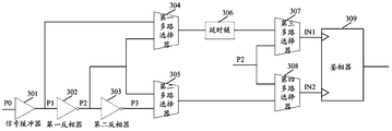
- the above-mentioned duty detection circuit 1053 includes a signal buffer 301, two inverters (including a first inverter 302 and a second inverter 303), and four multiplexers (including a first A multiplexer 304, a second multiplexer 305, a third multiplexer 307, and a fourth multiplexer 308) a delay chain 306 and a phase detector 309.
- the signal buffer 301 is coupled to the first inverter 302 and the first multiplexer 304.
- the first inverter 302 is coupled to the second inverter 303 and the first multiplexer. 304 and the second multiplexer 305, and the second inverter 303 is coupled to the second multiplexer 305.
- the first multiplexer 304 is coupled to the delay chain 306, the delay chain 306 is coupled to the third multiplexer 307, and the second multiplexer 305 is coupled to the fourth multiplexer 308.
- the first inverter 302 is also coupled to the third multiplexer 307 and the fourth multiplexer 308.
- the third multiplexer 307 and the fourth multiplexer 308 are respectively coupled to the phase detector 309.
- the reference clock signal input by the duty cycle detection circuit 1053 (that is, the above-mentioned signal buffer 301) is P0.
- the reference clock signal P0 passes through the signal buffer 301 to obtain a clock signal P1.
- the space ratio is the same as the reference clock signal P0 described above.
- the clock signal P1 passes through the first inverter 302 to obtain a clock signal P2.
- the frequency and amplitude of the clock signal P2 are the same as the clock signal P1, but the phase of the clock signal P2 is opposite to that of the clock signal P1.
- the duty cycle is equal to 1 minus the duty cycle of the clock signal P2; the clock signal P2 passes through the second inverter 303 to obtain a clock signal P3, and the frequency, amplitude and duty cycle of the clock signal P3 are the same as the above-mentioned clock signal P1 However, the phase of the clock signal P3 is opposite to that of the clock signal P2, that is, the phase of the clock signal P3 is the same as that of the clock signal P1.
- Mode 1 is to determine the duty cycle of the input signal by detecting the time T2 when the input signal is high; mode 2 is the time T1 to detect the input signal is low; mode 0 is to calibrate the phase detector 309.
- the first multiplexer 304 selects its first input signal (ie, the clock signal P1) and the second multiplexer. 305 strobes its second input signal (ie, clock signal P2. Clock signal P1 passes through the delay chain 306 to obtain a delayed clock signal P1.
- the third multiplexer 307 selects its first input signal (ie The delayed clock signal P1), that is, the first input signal (IN1) of the phase detector 309 is the delayed clock signal P1, and the fourth multiplexer 308 selects its second input signal (from The signal output from the second multiplexer 305), that is, the second input signal (IN2) of the phase detector 309 is a signal output from the second multiplexer 305.
- the timing diagrams of the above clock signals P0, P1, P2, and P3 are shown in FIG. 4A.
- the delay between the clock signal P2 and the clock signal P1 is INV1_D, that is, the clock signal is generated by the first inverter 302.
- the time delay is INV1_D
- the time delay between the clock signal P3 and the clock signal P2 is INV2_D, that is, the time delay caused by the clock signal passing through the second inverter 303 is INV2_D
- the duration of the flat signal is T1 and the duration of the high signal is T2. Since the clock signal P2 is obtained by the clock signal P1 through the inverter, the low signal duration of the clock signal P2 is T2 and the high signal duration is T1.
- the timing of the first input signal (IN1) and the second input signal (IN2) of the phase detector 309 is shown in FIG. 4B.
- the delays generated by the clock signal P1 after passing through the first multiplexer 304, the delay chain 306, and the third multiplexer 307 are MUX1_D, DLY_D, and MUX3_D, respectively.
- the clock signal P2 passes through the second multiplexer 305 and The delays generated after the fourth multiplexer 308 are MUX2_D and MUX4_D, respectively.
- the delay chain 306 generates a delay DLY_D for the clock signal P2.
- the first multiplexer 304 selects its second input signal (ie, the clock signal P2) and the second multiplexer. 305 strobes its second input signal (ie, the clock signal P2).
- the clock signal P2 passes through the delay chain 306 to obtain a delayed clock signal P2.
- the third multiplexer 307 selects its first input signal (that is, the delayed clock signal P2), that is, the first input signal (IN1) of the phase detector 309 is the delayed clock signal P2,
- the fourth multiplexer 308 selects its second input signal (that is, the signal output from the second multiplexer 305), that is, the second input signal (IN2) of the phase detector 309 is the second input signal (IN2) from the second multiplier. Signal output from the channel selector 305.
- the timing of the first input signal (IN1) and the second input signal (IN2) of the phase detector 309 is shown in FIG. 4C.
- the delays generated by the clock signal P2 after passing through the first multiplexer 304, the delay chain 306, and the third multiplexer 307 are MUX1_D, DLY_D, and MUX3_D, respectively.
- the clock signal P3 passes through the second multiplexer 305 and
- the delays generated after the fourth multiplexer 308 are MUX2_D and MUX4_D, respectively.
- the delay chain 306 generates a delay DLY_D for the clock signal P2.
- the delay time of the delay chain represents the relative relationship between T1 and T2.
- phase detector 309 obtains the delay duration DLY_D of the delay chain 309.
- the phase detector 309 presets three bit groups, including a coarse bit group, a medium bit group, and a fine bit group.
- the coarse adjustment bit group includes s1 bits
- the intermediate adjustment bit group includes s2 bits
- the fine adjustment bit group includes s3 bits.
- the phase detector 309 determines whether to perform coarse adjustment and intermediate adjustment.
- the phase detector 309 performs the coarse adjustment, as follows:
- the phase detector 309 waits for a first preset duration. The phase detector 309 then determines whether the rising edge of the first input signal (IN1) and the rising edge of the second input signal (IN2) are aligned, that is, whether the first input signal (IN1) and the second input signal (IN2) are aligned. There is a delay difference; when there is no delay difference between the first input signal (IN1) and the second input signal (IN2), the phase detector 309 sets the first bit position of the coarse adjustment bit group to 0; When there is a time delay difference between the input signal (IN1) and the second input signal (IN2), the phase detector 309 sets the first bit position of the coarse adjustment bit group to 1.
- the phase detector 309 repeatedly executes the above-mentioned process s1, and after performing the above-mentioned process s1, the s1 bits of the coarse adjustment bit group are all set to 0 or 1, and s1 is an integer greater than 1.
- the coarse adjustment bit group can be regarded as a character string composed of 0 and 1.
- phase detector 309 performs the middle adjustment, and the middle adjustment process is similar to the coarse adjustment process described above. details as follows:
- the phase detector 309 waits for a second preset duration. The phase detector 309 then determines whether there is a delay difference between the first input signal (IN1) and the second input signal (IN2); when there is no delay difference between the first input signal (IN1) and the second input signal (IN2) When the phase detector 309 sets the first bit position of the middle bit group to 0, when there is a delay difference between the first input signal (IN1) and the second input signal (IN2), the phase detector 309 sets the above The first bit position of the middle bit group is set.
- the phase detector 309 repeatedly executes the above-mentioned process s2 times, and after performing the above-mentioned process s2 times, the s2 bits of the coarse adjustment bit group are all set to 0 or 1, and s1 is an integer greater than 1.
- the middle bit group can be regarded as a character string composed of 0 and 1.
- the phase detector 309 When it is determined to skip the coarse adjustment and the middle adjustment, the phase detector 309 directly enters the fine adjustment.
- the fine adjustment process is similar to the coarse and middle adjustment process described above, and will not be described here.
- the fine-tuning bit group can be regarded as a string composed of 0 and 1.
- the phase detector 309 determines the delay time of the delay chain according to the coarse adjustment bit group, the medium adjustment bit group, and the fine adjustment bit group. Specifically, the phase detector 309 obtains the number of bits set to 1 in the coarse tuning bit group, the medium tuning bit group, and the fine tuning bit group, respectively.
- the number of bits set to 1 in the coarse bit group, the medium bit group, and the fine bit group is n1, n2, and n3, respectively.
- the delay time represented by each bit set to 1 in the coarse tuning bit group is t1 seconds
- the delay time represented by each bit set in the medium tuning bit group is 1 t2 seconds.
- the delay time represented by each bit set to 1 in the coarse tuning bit group is 0.5 nanosecond
- the delay time represented by each bit set in the above medium tuning bit group is 15 picoseconds.
- the delay time of each bit set to 1 in the fine adjustment bit group is 500 femtoseconds
- the phase detector 309 can obtain the delay time DLY_D of the delay chain.
- the above-mentioned duty cycle detection circuit further includes a microprocessor, which is configured to adjust the generation of the clock signal output by the first multiplexer 304 when the working mode is the mode 1 and the mode 2 So that the delay difference between the first input signal and the second input signal of the phase detector 309 is 0.
- the microprocessor obtains whether the phases of the two input signals (ie, IN1 and IN2) detected by the phase detector are 0.
- the microprocessor increases the delay
- the time delay of the first input signal of the third multiplexer 307 by the time chain increases the delay of the first input signal (ie, IN1) of the phase detector 309, so that the two inputs of the phase detector 309
- the phase difference of the signal decreases; when the phase detector 309 determines that the phase difference between its two input signals is not 0 and the first input signal (IN1) lags behind the second input signal (IN2), the microprocessor decreases The delay of the first input signal of the third demultiplexer 307 by the delay chain, thereby reducing the delay of the first input signal (ie, IN1) of the phase detector 309, making the two of the phase detector 309 two The phase
- the third multiplexer 307 selects its second input signal and the fourth multiplexer 308 selects its first An input signal, that is, the first input signal and the second input signal of the phase detector 309 are both P2. Because the delays of P2 by the third multiplexer 307 and the fourth multiplexer 308 are the same, the phase difference between the two signals input to the phase detector 309 is zero. In other words, the third multiplexer 307 and the fourth multiplexer 308 gate the same input signal into the phase detector 309. As shown in FIG. 4D, the phase difference between the first input signal (ie, IN1) and the second input signal (ie, IN2) of the phase detector 309 is 0.
Abstract
Disclosed in the present invention is a reference clock duty ratio calibration circuit, comprising a low-noise low-dropout regulator, an oscillation circuit, a duty ratio adjustment circuit and a duty ratio calibration circuit. The duty ratio detection circuit of the reference clock duty ratio calibration circuit detects the duty ratio of a reference clock signal outputted by the duty ratio adjustment circuit, and when it is determined that the duty ratio of the reference clock signal deviates from a preset duty ratio, the duty ratio detection circuit adjusts the amplitude of the output signal thereof, and the duty ratio of the reference clock signal outputted by the duty ratio adjustment circuit is adjusted by means of the output voltage of the digital-to-analog conversion circuit and the output voltage of the low-noise low-voltage differential regulator. The reference clock duty ratio calibration circuit of the present invention can be used to effectively reduce the noise of the reference clock, improving the communication performance.
Description
本申请涉及电路领域,特别涉及一种参考时钟占空比校准电路。The present application relates to the field of circuits, and in particular, to a reference clock duty cycle calibration circuit.
现代通信中,无线通信技术占主导地位,比如终端无线通讯、短距离无线通讯以及大型公共网络无线通讯。随着无线通信的发展,对数据传输的质量和速度的要求越来越高。In modern communications, wireless communication technologies dominate, such as terminal wireless communications, short-range wireless communications, and large public network wireless communications. With the development of wireless communication, the requirements for the quality and speed of data transmission are getting higher and higher.
为了提高数据传输的质量和速度,在802.11ac标准中提出了更高的射频带宽(提高至160MHz),更多的多输入多输出(multiple input multiple output,MIMO)和更高阶的调制。这就要求发射机的RMS EVM达到-32dB,在发射机线性度达到要求的前提下,最主要限制来源于锁相环的相位噪声。参考时钟噪声是当前PLL的相位噪声主要来源之一,因此改善参考时钟噪声成为提高通信性能的必要条件。In order to improve the quality and speed of data transmission, higher radio frequency bandwidth (up to 160 MHz), more multiple input multiple output (MIMO) and higher order modulation are proposed in the 802.11ac standard. This requires the transmitter's RMS EVM to reach -32dB. Under the premise that the transmitter linearity meets the requirements, the most important limitation is the phase noise of the phase-locked loop. Reference clock noise is one of the main sources of phase noise for current PLLs, so improving reference clock noise becomes a necessary condition for improving communication performance.
发明内容Summary of the Invention
本发明实施例公开了一种参考时钟占空比校准电路,采用该电路能够有效改善参考时钟的噪声,提高通信性能。The embodiment of the invention discloses a reference clock duty cycle calibration circuit, which can effectively improve the noise of the reference clock and improve the communication performance.
第一方面,本发明实施例提供了一种参考时钟占空比校准电路,包括:第一低噪声低压差稳压器,用于提供低噪声电压;振荡电路,用于在所述低噪声电压的提供驱动下,产生正弦波信号;占空比调节电路,用于根据第一参考电压和所述正弦波信号调整第一参考时钟信号的占空比;占空比校准电路,包括:占空比检测电路,用于检测所述第一参考时钟信号的占空比,并根据所述第一参考时钟信号的占空比调整所述占空比检测电路输出信号的幅值;第二低噪声低压差稳压器,用于根据所述占空比检测电路输出信号的幅值,调整并输出所述第一参考电压,所述第一参考电压值与所述占空比检测电路输出信号的幅值成正比。通过低噪声电压驱动的振荡电路产生的正弦波信号具有低噪声的特性,使得该参考时钟占空比校准电路输出的信号也具有低噪声特性,有效改善参考时钟的噪声,提高通信性能。In a first aspect, an embodiment of the present invention provides a reference clock duty cycle calibration circuit, including: a first low-noise low-dropout voltage regulator for providing a low-noise voltage; and an oscillating circuit for the low-noise voltage Driven by a sine wave signal, a duty cycle adjustment circuit is configured to adjust the duty cycle of the first reference clock signal according to the first reference voltage and the sine wave signal. The duty cycle calibration circuit includes: Ratio detection circuit, configured to detect the duty cycle of the first reference clock signal, and adjust the amplitude of the output signal of the duty cycle detection circuit according to the duty cycle of the first reference clock signal; the second low noise The low-dropout voltage regulator is configured to adjust and output the first reference voltage according to the amplitude of the output signal of the duty cycle detection circuit. The amplitude is directly proportional. The sine wave signal generated by the low-noise voltage-driven oscillation circuit has low-noise characteristics, so that the signal output by the reference clock duty cycle calibration circuit also has low-noise characteristics, which effectively improves the noise of the reference clock and improves communication performance.
在一种可行的实施例中,所述振荡电路产生的所述正弦波信号,以直流耦合的方式输入所述占空比调节电路。In a feasible embodiment, the sine wave signal generated by the oscillating circuit is input to the duty cycle adjusting circuit in a DC coupling manner.
在一种可行的实施例中,所述占空比检测电路根据所述第一参考时钟信号的占空比调整所述占空比检测电路输出信号的幅值,包括:In a feasible embodiment, adjusting the duty cycle of the output signal of the duty cycle detection circuit according to the duty cycle of the first reference clock signal by the duty cycle detection circuit includes:
所述占空比检测电路,用于检测所述第一参考时钟信号的占空比是否偏离预设占空比;The duty cycle detection circuit is configured to detect whether the duty cycle of the first reference clock signal deviates from a preset duty cycle;
所述占空比检测电路,还用于当确定所述第一参考时钟信号的占空比偏离预设占空比时,调整所述占空比检测电路输出信号的幅值;当确定所述第一参考时钟信号的占空比未偏离预设占空比时,不调整所述占空比检测电路输出信号的幅值。The duty cycle detection circuit is further configured to adjust an amplitude of an output signal of the duty cycle detection circuit when it is determined that the duty cycle of the first reference clock signal deviates from a preset duty cycle; When the duty cycle of the first reference clock signal does not deviate from the preset duty cycle, the amplitude of the output signal of the duty cycle detection circuit is not adjusted.
在一种可行的实施例中,所述占空比检测电路用于当所述第一参考时钟信号的占空比偏离预设占空比时,调整所述占空比检测电路输出信号的幅值,具体包括:In a feasible embodiment, the duty cycle detection circuit is configured to adjust the amplitude of an output signal of the duty cycle detection circuit when the duty cycle of the first reference clock signal deviates from a preset duty cycle. Values, including:
当连续N次检测到所述第一参考时钟信号的占空比大于所述预设占空比时,所述占空 比检测电路增大其输出信号的幅值,所述N为大于1的整数;When it is detected that the duty ratio of the first reference clock signal is greater than the preset duty ratio for N consecutive times, the duty ratio detection circuit increases the amplitude of its output signal, where N is greater than 1. Integer
当连续M次检测到所述第一参考时钟信号的占空比小于所述预设占空比时,所述占空比检测电路减小其输出信号的幅值,所述M为大于1的整数。由于第一参考电压值与所述占空比检测电路输出信号的幅值成正比,通过调整占空比检测电路输出信号的幅值可以实现对第一参考电压的调整,实现占空比调节电路对第一参考时钟信号的占空比的调整,进而达到对该参考时钟占空比校准电路输出信号的占空比的动态调整。When it is detected that the duty ratio of the first reference clock signal is less than the preset duty ratio for M consecutive times, the duty ratio detection circuit reduces the amplitude of its output signal, where M is greater than 1. Integer. Because the first reference voltage value is proportional to the amplitude of the output signal of the duty cycle detection circuit, the first reference voltage can be adjusted by adjusting the amplitude of the output signal of the duty cycle detection circuit, and the duty cycle adjustment circuit can be implemented. The duty cycle of the first reference clock signal is adjusted, thereby achieving dynamic adjustment of the duty cycle of the output signal of the reference clock duty cycle calibration circuit.
在一种可行的实施例中,所述占空比检测电路获取所述第一参考时钟信号的占空比,包括:In a feasible embodiment, the obtaining the duty cycle of the first reference clock signal by the duty cycle detecting circuit includes:
所述占空比检测电路,用于获取所述第一参考时钟信号的高电平时长或低电平时长;The duty cycle detection circuit is configured to obtain a high-level duration or a low-level duration of the first reference clock signal;
所述占空比检测电路,用于根据所述第一参考时钟信号的周期与所述第一参考时钟信号的高电平时长或低电平时长确定所述第一参考时钟信号的占空比。The duty cycle detection circuit is configured to determine a duty cycle of the first reference clock signal according to a period of the first reference clock signal and a high-level duration or a low-level duration of the first reference clock signal. .
在一种可行的实施例中,所述预设占空比为50%。In a feasible embodiment, the preset duty cycle is 50%.
在一种可行的实施例中,所述占空比校准电路还包括:In a feasible embodiment, the duty cycle calibration circuit further includes:
数模转换电路,用于将所述占空比检测电路的输出信号转换为第二参考电压,并将所述第二参考电压输入至所述第二低噪声低压差稳压器,以调整所述第二低噪声低压差稳压器输出的第一参考电压。A digital-to-analog conversion circuit, configured to convert an output signal of the duty cycle detection circuit into a second reference voltage, and input the second reference voltage to the second low-noise low-dropout voltage regulator to adjust the The first reference voltage output from the second low-noise low-dropout voltage regulator is described.
在一种可行的实施例中,所述占空比调节电路包括:第一晶体管Q1和第二晶体管Q2;In a feasible embodiment, the duty cycle adjustment circuit includes: a first transistor Q1 and a second transistor Q2;
所述第一晶体管Q1的源极耦合到所述占空比校准电路,所述第一晶体管Q1的栅极和所述第二晶体管Q2的栅极均耦合到所述振荡电路,所述第一晶体管Q1的漏极和所述第二晶体管Q2的漏极均耦合到所述占空比校准电路,所述第二晶体管Q2的源极耦合到地;A source of the first transistor Q1 is coupled to the duty cycle calibration circuit, and a gate of the first transistor Q1 and a gate of the second transistor Q2 are both coupled to the oscillation circuit. The drain of the transistor Q1 and the drain of the second transistor Q2 are both coupled to the duty cycle calibration circuit, and the source of the second transistor Q2 is coupled to the ground;
当所述第一晶体管Q1的源极电压增大时,所述第一参考时钟信号的占空比减小;当所述第一晶体管Q2的源极电压减小时,所述第一参考时钟信号的占空比增大。When the source voltage of the first transistor Q1 increases, the duty cycle of the first reference clock signal decreases; when the source voltage of the first transistor Q2 decreases, the first reference clock signal The duty cycle increases.
在一种可行的实施例中,所述参考时钟占空比校准电路还包括;In a feasible embodiment, the reference clock duty cycle calibration circuit further includes:
二倍频电路,用于将所述第一参考时钟信号转换为第二参考时钟信号,所述第二参考时钟信号的频率为所述第一参考信号的两倍。A double frequency circuit is used to convert the first reference clock signal into a second reference clock signal, and the frequency of the second reference clock signal is twice that of the first reference signal.
可以看出,在本发明实施例的方案中,参考时钟占空比校准电路的占空比检测电路检测占空比调节电路输出的参考时钟信号的占空比,当确定该参考时钟信号的占空比偏离预设占空比时,上述占空比检测电路调整其输出信号的幅值,从而使数模转换电路的输出电压发生变化。由于上述数模转换电路输出的电压为第二低噪声稳压器的参考电压,并且第二低噪声低压差稳压器大的输出电压与其参考电压成正比,故第二低噪声低压差稳压器的输出电压随着占空比检测电路的输出电压的变化而变化。又由于占空比调节电路输出的参考时钟信号的占空比与占空比检测电路的参考电压成反比,而第二低噪声低压差稳压器的输出电压为占空比调节电路的参考电压,因此可以通过调整第二低噪声低压差稳压器的输出电压来调节占空比调节电路输出的参考时钟信号的占空比。采用本发明的参考时钟占空比校准电路能够有效改善参考时钟的噪声,提高通信性能。It can be seen that, in the solution of the embodiment of the present invention, the duty cycle detection circuit of the reference clock duty cycle calibration circuit detects the duty cycle of the reference clock signal output by the duty cycle adjustment circuit. When the duty ratio deviates from the preset duty cycle, the above-mentioned duty cycle detection circuit adjusts the amplitude of its output signal, so that the output voltage of the digital-to-analog conversion circuit changes. Because the voltage output by the digital-to-analog conversion circuit is the reference voltage of the second low-noise regulator, and the large output voltage of the second low-noise low-dropout regulator is proportional to its reference voltage, the second low-noise low-dropout regulator The output voltage of the converter changes with the output voltage of the duty cycle detection circuit. Because the duty cycle of the reference clock signal output by the duty cycle adjustment circuit is inversely proportional to the reference voltage of the duty cycle detection circuit, the output voltage of the second low noise low dropout voltage regulator is the reference voltage of the duty cycle adjustment circuit. Therefore, the duty cycle of the reference clock signal output by the duty cycle adjustment circuit can be adjusted by adjusting the output voltage of the second low-noise low-dropout voltage regulator. The reference clock duty cycle calibration circuit of the invention can effectively improve the noise of the reference clock and improve the communication performance.
为了更清楚地说明本发明实施例中的技术方案,下面将对实施例或现有技术描述中所 需要使用的附图作简单地介绍,显而易见地,下面描述中的附图仅仅是本发明的一些实施例,对于本领域普通技术人员来讲,在不付出创造性劳动的前提下,还可以根据这些附图获得其他的附图。In order to explain the technical solutions in the embodiments of the present invention more clearly, the drawings used in the embodiments or the description of the prior art will be briefly introduced below. Obviously, the drawings in the following description are only the present invention. In some embodiments, for those of ordinary skill in the art, other drawings may be obtained based on these drawings without paying creative labor.
图1为本发明实施例提供的一种参考时钟占空比校准电路的示意图;1 is a schematic diagram of a reference clock duty cycle calibration circuit according to an embodiment of the present invention;
图2为本发明实施例提供的一种占空比调节电路的结构和工作原理示意图;FIG. 2 is a schematic diagram of a structure and a working principle of a duty cycle adjusting circuit according to an embodiment of the present invention; FIG.
图3a为本发明实施例提供的一种占空比检测电路的结构示意图;3a is a schematic structural diagram of a duty cycle detection circuit according to an embodiment of the present invention;
图3b为本发明实施例提供的一种占空比检测电路在模式1下信号流向示意图;3b is a schematic diagram of a signal flow direction of a duty cycle detection circuit in mode 1 according to an embodiment of the present invention;
图3c为本发明实施例提供的一种占空比检测电路在模式2下信号流向示意图;3c is a schematic diagram of a signal flow direction of a duty cycle detection circuit in mode 2 according to an embodiment of the present invention;
图3d为本发明实施例提供的一种占空比检测电路在模式0下信号流向示意图;3d is a schematic diagram of a signal flow direction of a duty cycle detection circuit in mode 0 according to an embodiment of the present invention;
图4为本发明实施例提供的一种占空比检测电路的时钟信号时序示意图。FIG. 4 is a schematic timing diagram of a clock signal of a duty cycle detection circuit according to an embodiment of the present invention.
下面将结合本发明实施例中的附图,对本发明实施例中的技术方案进行清楚、完整地描述。The technical solutions in the embodiments of the present invention will be clearly and completely described below with reference to the drawings in the embodiments of the present invention.
参见图1,图1为本发明实施例提供的一种参考时钟占空比校准电路的示意图。如图1所示,该参考时钟占空比校准电路包括第一低噪声低压差稳压器101,振荡电路102、占空比调节电路103、二倍频电路104和占空比校准电路105。Referring to FIG. 1, FIG. 1 is a schematic diagram of a reference clock duty cycle calibration circuit according to an embodiment of the present invention. As shown in FIG. 1, the reference clock duty cycle calibration circuit includes a first low noise low dropout voltage regulator 101, an oscillation circuit 102, a duty cycle adjustment circuit 103, a double frequency circuit 104 and a duty cycle calibration circuit 105.
其中,上述第一低噪声低压差稳压器101耦合到上述振荡电路102,该振荡电路102产生的正弦波信号,以直流耦合的方式输入上述占空比调节电路103。该占空比调节电路103耦合到上述占空比校准电路105。上述占空比校准电路105耦合到上述占空比调节电路103;上述占空比调节电路103耦合到上述二倍频电路104。The first low-noise low-dropout voltage regulator 101 is coupled to the oscillating circuit 102, and a sine wave signal generated by the oscillating circuit 102 is input to the above-mentioned duty cycle adjusting circuit 103 in a DC coupling manner. The duty cycle adjustment circuit 103 is coupled to the above-mentioned duty cycle calibration circuit 105. The duty cycle calibration circuit 105 is coupled to the duty cycle adjustment circuit 103; the duty cycle adjustment circuit 103 is coupled to the double frequency circuit 104.
上述第一低噪声低压差稳压器101输出的电压为低噪声电压,该低噪声电源用于驱动上述振荡电路102,以使该振荡电路102产生时钟信号,该时钟信号为正弦波信号,且上述第一低噪声低压差稳压器101输出的低噪声电压为直流电压。该振荡电路102将产生的时钟信号输入到上述占空比调节电路103,该占空比调节电路103根据上述占空比校准电路105的第二低噪声低压差稳压器1051提供的第一参考电压调整根据上述振荡电路102提供的正弦波信号产生的第一参考时钟信号的占空比,该第一参考时钟信号为方波信号。上述第一参考电压为幅值可调的低噪声直流电压。The voltage output by the first low-noise low-dropout voltage regulator 101 is a low-noise voltage, and the low-noise power supply is used to drive the oscillating circuit 102 so that the oscillating circuit 102 generates a clock signal, which is a sine wave signal, and The low-noise voltage output by the first low-noise low-dropout voltage regulator 101 is a DC voltage. The oscillating circuit 102 inputs the generated clock signal to the above-mentioned duty cycle adjustment circuit 103. The duty cycle adjustment circuit 103 is based on the first reference provided by the second low-noise low-dropout voltage regulator 1051 of the above-mentioned duty cycle calibration circuit 105. The voltage is adjusted according to the duty cycle of the first reference clock signal generated by the sine wave signal provided by the oscillation circuit 102, and the first reference clock signal is a square wave signal. The first reference voltage is a low-noise DC voltage with adjustable amplitude.
上述占空比校准电路105包括:占空比检测电路1053和与该占空比检测电路1053耦合的第二低噪声低压差稳压器1051;The above-mentioned duty cycle calibration circuit 105 includes: a duty cycle detection circuit 1053 and a second low-noise low-dropout voltage regulator 1051 coupled to the duty cycle detection circuit 1053;
上述占空比检测电路1053,用于检测上述第一参考时钟信号的占空比,并根据该第一参考时钟信号的占空比调整上述占空比检测电路1053输出信号的幅值;The duty cycle detection circuit 1053 is configured to detect the duty cycle of the first reference clock signal, and adjust the amplitude of the output signal of the duty cycle detection circuit 1053 according to the duty cycle of the first reference clock signal;
上述第二低噪声低压差稳压器,用于根据所述占空比检测电路输出信号的幅值,调整并输出上述第一参考电压,该第一参考电压的幅值与上述占空比检测电路输出信号的幅值成正比。The second low-noise low-dropout voltage regulator is configured to adjust and output the first reference voltage according to the amplitude of the output signal of the duty cycle detection circuit, and the amplitude of the first reference voltage is related to the duty cycle detection. The amplitude of the circuit output signal is proportional.
上述占空比校准电路105还包括:The above-mentioned duty cycle calibration circuit 105 further includes:
数模转换电路1052,用于将上述占空比检测电路1053的输出信号转换为第二参考电压,并将该第二参考电压输入至上述第二低噪声低压差稳压器1051,以调整上述第二低噪 声低压差稳压器1051输出的第一参考电压。A digital-to-analog conversion circuit 1052, configured to convert the output signal of the duty ratio detection circuit 1053 into a second reference voltage, and input the second reference voltage to the second low-noise low-dropout voltage regulator 1051 to adjust the above-mentioned A first reference voltage output from the second low-noise low-dropout regulator 1051.
其中,上述第二参考电压与上述占空比检测电路1053输出信号的幅值成正比,且第一参考电压与上述第二参考电压成正比,即上述第一参考电压与上述占空比检测电路1053输出信号的幅值成正比。The second reference voltage is proportional to the amplitude of the output signal of the duty cycle detection circuit 1053, and the first reference voltage is proportional to the second reference voltage, that is, the first reference voltage is proportional to the duty cycle detection circuit. The amplitude of the 1053 output signal is directly proportional.
具体地,所述占空比检测电路1053用于当所述第一参考时钟信号的占空比偏离预设占空比时,调整所述占空比检测电路1053输出信号的幅值,具体包括:Specifically, the duty cycle detection circuit 1053 is configured to adjust the amplitude of the output signal of the duty cycle detection circuit 1053 when the duty cycle of the first reference clock signal deviates from a preset duty cycle, and specifically includes: :
当连续N次检测到所述第一参考时钟信号的占空比大于所述预设占空比时,所述占空比检测电路1053增大其输出信号的幅值,所述N为大于1的整数;When it is detected that the duty cycle of the first reference clock signal is greater than the preset duty ratio N consecutive times, the duty cycle detection circuit 1053 increases the amplitude of its output signal, where N is greater than 1 An integer
当连续M次检测到所述第一参考时钟信号的占空比小于所述预设占空比时,所述占空比检测电路1053减小其输出信号的幅值,所述M为大于1的整数,且M与N相等或者不相等。When it is detected that the duty ratio of the first reference clock signal is less than the preset duty ratio for M consecutive times, the duty ratio detection circuit 1053 reduces the amplitude of its output signal, where M is greater than 1 Is an integer and M is equal to or not equal to N.
可选地,预设占空比为50%。Optionally, the preset duty cycle is 50%.
其中,上述占空比检测电路1053获取上述第一参考时钟信号的占空比,包括:The duty cycle detection circuit 1053 obtains the duty cycle of the first reference clock signal, including:
上述占空比检测电路1053获取上述第一参考时钟信号的高电平时长或低电平时长;并根据上述第一参考时钟信号的周期与上述第一参考时钟信号的高电平时长或低电平时长确定上述第一参考时钟信号的占空比。The duty cycle detection circuit 1053 obtains the high-level duration or the low-level duration of the first reference clock signal; and according to the period of the first reference clock signal and the high-level duration or low voltage of the first reference clock signal The time period determines the duty cycle of the first reference clock signal.
其中,上述占空比检测电路1053的输出信号的幅值与上述第一参考电压值成正比。The amplitude of the output signal of the duty cycle detection circuit 1053 is proportional to the first reference voltage value.
下面具体介绍上述占空比调节电路103的工作原理。该占空比调节电路103的结构如图2的a图所示,该占空比调节电路包括两个晶体管:第一晶体管Q1和第二场效应管Q2。上述第一晶体管Q1的源极(s)耦合到上述占空比校准电路,上述第一晶体管Q1的栅极(g)和上述第二晶体管Q2的栅极(g)均耦合到上述振荡电路,上述第一晶体管Q1的漏极(d)和上述第二晶体管Q2的漏极(d)均耦合到上述占空比校准电路,上述第二晶体管Q2的源极(s)耦合到地;The working principle of the above-mentioned duty cycle adjustment circuit 103 is specifically described below. The structure of the duty cycle adjustment circuit 103 is shown in FIG. 2A. The duty cycle adjustment circuit includes two transistors: a first transistor Q1 and a second field effect transistor Q2. The source (s) of the first transistor Q1 is coupled to the duty cycle calibration circuit, and the gate (g) of the first transistor Q1 and the gate (g) of the second transistor Q2 are coupled to the oscillation circuit. The drain (d) of the first transistor Q1 and the drain (d) of the second transistor Q2 are both coupled to the duty cycle calibration circuit, and the source (s) of the second transistor Q2 is coupled to ground;
当上述第一晶体管Q1的源极电压增大时,上述第一参考时钟信号的占空比减小;当上述第一晶体管Q2的源极电压减小时,上述第一参考时钟信号的占空比增大。When the source voltage of the first transistor Q1 increases, the duty cycle of the first reference clock signal decreases; when the source voltage of the first transistor Q2 decreases, the duty cycle of the first reference clock signal Increase.
上述第二低噪声低压差稳压器的输出电压为VDD_LDO,即上述第一参考电压为VDD_LDO。The output voltage of the second low-noise low-dropout voltage regulator is VDD_LDO, that is, the first reference voltage is VDD_LDO.
需要指出的是,上述晶体管Q1和Q2均为金属氧化物场效应晶体管。It should be noted that the above-mentioned transistors Q1 and Q2 are both metal oxide field effect transistors.
如图2的b图所示,第一参考时钟信号的周期为T
ref,当VDD_LDO=VDD_LDO1时,上述占空比调节电路103输出的高电平时间为t
1,此时占空比调节电路103输出的第一参考时钟信号的占空比为t
1/T
ref;当VDD_LDO=VDD_LDO2时,上述占空比调节电路103输出的高电平时间为t
2,此时占空比调节电路103输出的第一参考时钟信号的占空比为t
2/T
ref。由图2的b图可知,上述t
2>t
1,故t
2/T
ref>t
1/T
ref,因此可以通过调节占空比调节电路103输入的直流电压(即第一参考电压)的大小来调节上述第一参考时钟信号的占空比。
As shown in Figure 2b, the period of the first reference clock signal is T ref . When VDD_LDO = VDD_LDO1, the high-level time output by the above-mentioned duty cycle adjustment circuit 103 is t 1. At this time, the duty cycle adjustment circuit The duty cycle of the first reference clock signal output by 103 is t 1 / T ref ; when VDD_LDO = VDD_LDO2, the high-level time output by the above-mentioned duty cycle adjustment circuit 103 is t 2. At this time, the duty cycle adjustment circuit 103 The duty cycle of the output first reference clock signal is t 2 / T ref . It can be known from the b diagram in FIG. 2 that the above t 2 > t 1 , so t 2 / T ref > t 1 / T ref . Therefore, the DC voltage (ie, the first reference voltage) input by adjusting the duty cycle adjustment circuit 103 can be adjusted. Size to adjust the duty cycle of the first reference clock signal.
当上述占空比调节电路103的第一参考电压增大时,该占空比调节电路103输出的第一参考时钟信号的占空比减小;当上述占空比调节电路103的第一参考电压减小时,该占空比调节电路103输出的第一参考时钟信号的占空比增大。由此可以反推,当上述占空比检测电路1053确定上述第一参考时钟信号的占空比大于上述预设占空比时,上述占空比检 测电路1053增大其输出信号的幅值,从而提高上述第二低噪声低压差稳压器1051的参考电压(即上述第二参考电压)。由于上述第二低噪声低压差稳压器1051的输出信号的电压与上述第二参考电压成正比,因此上述占空比调节电路103的参考电压增大,进而使得上述第一参考时钟信号的占空比减小;反之,当上述占空比检测电路1053确定上述第一参考时钟信号的占空比小于上述预设占空比时,上述占空比检测电路1053减小其输出信号的幅值,从而降低上述第二低噪声低压差稳压器1051的参考电压(即上述第二参考电压)。由于上述第二低噪声低压差稳压器1051的输出信号的电压与上述第二参考电压成正比,因此上述占空比调节电路103的参考电压减小,进而使得上述第一参考时钟信号的占空比增大。When the first reference voltage of the duty cycle adjustment circuit 103 increases, the duty cycle of the first reference clock signal output by the duty cycle adjustment circuit 103 decreases; when the first reference voltage of the duty cycle adjustment circuit 103 increases, When the voltage decreases, the duty cycle of the first reference clock signal output by the duty cycle adjustment circuit 103 increases. It can be deduced from this that when the duty cycle detection circuit 1053 determines that the duty cycle of the first reference clock signal is greater than the preset duty cycle, the duty cycle detection circuit 1053 increases the amplitude of its output signal. Therefore, the reference voltage of the second low-noise low-dropout voltage regulator 1051 (that is, the second reference voltage) is increased. Because the voltage of the output signal of the second low-noise low-dropout voltage regulator 1051 is proportional to the second reference voltage, the reference voltage of the duty cycle adjustment circuit 103 increases, thereby further occupying the first reference clock signal. The air-to-air ratio decreases; conversely, when the duty cycle detection circuit 1053 determines that the duty cycle of the first reference clock signal is less than the preset duty cycle, the duty cycle detection circuit 1053 reduces the amplitude of its output signal , Thereby reducing the reference voltage of the second low-noise low-dropout voltage regulator 1051 (ie, the second reference voltage). Because the voltage of the output signal of the second low-noise low-dropout voltage regulator 1051 is proportional to the second reference voltage, the reference voltage of the duty cycle adjustment circuit 103 is reduced, thereby further occupying the first reference clock signal. The air ratio increases.
在一种可行的实施例中,上述参考时钟占空比校准电路还包括二倍频电路104,该二倍频电路104耦合到上述占空比调节电路。In a feasible embodiment, the reference clock duty cycle calibration circuit further includes a double frequency circuit 104 which is coupled to the above-mentioned duty cycle adjustment circuit.
其中,上述二倍频电路104包括延时电路和异或门电路。上述延时电路耦合到上述异或门电路,且上述延时电路和异或门电路耦合到到上述占空比调节电路。The double-frequency circuit 104 includes a delay circuit and an exclusive-OR gate circuit. The delay circuit is coupled to the XOR circuit, and the delay circuit and the XOR circuit are coupled to the duty cycle adjustment circuit.
上述占空比调节电路103输出的第一参考时钟信号同时驱动上述二倍频电路104和上述占空比校准电路105的占空比检测电路1053。The first reference clock signal output from the duty cycle adjustment circuit 103 drives the duty cycle detection circuit 1053 of the double frequency circuit 104 and the duty cycle calibration circuit 105 simultaneously.
具体地,上述占空比调节电路103将输出的参考时钟信号直接输入到上述二倍频电路的异或门电路和延时电路,上述延时电路对占空比调节电路输出的参考时钟信号进行延时,然后将延时后的参考时钟信号输入到上述异或门电路。上述参考时钟信号和延时后的参考时钟信号通过上述异或门后,得到2倍频的参考时钟信号。比如上述参考时钟信号的频率为f
ref,幅度为V,则2倍频的参考时钟信号的频率f=2f
ref,幅值为V。
Specifically, the duty cycle adjustment circuit 103 directly inputs the output reference clock signal to the XOR gate circuit and the delay circuit of the double frequency circuit, and the delay circuit performs the reference clock signal output from the duty cycle adjustment circuit. Delay, and then input the delayed reference clock signal to the above-mentioned XOR circuit. After the reference clock signal and the delayed reference clock signal pass through the XOR gate, a reference frequency signal with a frequency of 2 is obtained. For example, the frequency of the above reference clock signal is f ref and the amplitude is V, then the frequency of the reference clock signal of 2 times frequency f = 2f ref and the amplitude is V.
需要说明的是,本申请对上述延时电路对参考时钟信号进行延时的时长不做限定。It should be noted that, in this application, the duration of the delay of the reference clock signal by the delay circuit is not limited.
下面具体介绍上述占空比检测电路1053的结构框架及工作原理。The structural framework and working principle of the above-mentioned duty cycle detection circuit 1053 are specifically introduced below.
如图3a所示,上述占空比检测电路1053包括信号缓冲器301、两个反相器(包括第一反相器302和第二反相器303),四个多路选择器(包括第一多路选择器304、第二多路选择器305、第三多路选择器307和第四多路选择器308)延时链306和鉴相器309。As shown in FIG. 3a, the above-mentioned duty detection circuit 1053 includes a signal buffer 301, two inverters (including a first inverter 302 and a second inverter 303), and four multiplexers (including a first A multiplexer 304, a second multiplexer 305, a third multiplexer 307, and a fourth multiplexer 308) a delay chain 306 and a phase detector 309.
其中,上述信号缓冲器301耦合到上述第一反相器302和上述第一多路选择器304,该第一反相器302耦合到上述第二反相器303、上述第一多路选择器304和上述第二多路选择器305,上述第二反相器303耦合到上述第二多路选择器305。上述第一多路选择器304耦合到上述延时链306,该延时链306耦合到上述第三多路选择器307,上述第二多路选择器305耦合到上述第四多路选择器308;上述第一反相器302还耦合到上述第三多路选择器307和上述第四多路选择器308。上述第三多路选择器307和上述第四多路选择器308分别耦合到上述鉴相器309。The signal buffer 301 is coupled to the first inverter 302 and the first multiplexer 304. The first inverter 302 is coupled to the second inverter 303 and the first multiplexer. 304 and the second multiplexer 305, and the second inverter 303 is coupled to the second multiplexer 305. The first multiplexer 304 is coupled to the delay chain 306, the delay chain 306 is coupled to the third multiplexer 307, and the second multiplexer 305 is coupled to the fourth multiplexer 308. The first inverter 302 is also coupled to the third multiplexer 307 and the fourth multiplexer 308. The third multiplexer 307 and the fourth multiplexer 308 are respectively coupled to the phase detector 309.
上述占空比检测电路1053(即上述信号缓冲器301)输入的参考时钟信号为P0,该参考时钟信号P0经过该信号缓冲器301得到时钟信号P1,该时钟信号P1的频率、幅值和占空比与上述参考时钟信号P0相同。上述时钟信号P1经过上述第一反相器302得到时钟信号P2,该时钟信号P2的频率和幅值与时钟信号P1相同,但时钟信号P2的相位与时钟信号P1的相反,且时钟信号P1的占空比等于1减去时钟信号P2的占空比;时钟信号P2经过上述第二反相器303得到时钟信号P3,该时钟信号P3的频率、幅值和占空比与上述时 钟信号P1相同,但时钟信号P3的相位与上述时钟信号P2的相反,即该时钟信号P3的相位与上述时钟信号P1的相同。The reference clock signal input by the duty cycle detection circuit 1053 (that is, the above-mentioned signal buffer 301) is P0. The reference clock signal P0 passes through the signal buffer 301 to obtain a clock signal P1. The space ratio is the same as the reference clock signal P0 described above. The clock signal P1 passes through the first inverter 302 to obtain a clock signal P2. The frequency and amplitude of the clock signal P2 are the same as the clock signal P1, but the phase of the clock signal P2 is opposite to that of the clock signal P1. The duty cycle is equal to 1 minus the duty cycle of the clock signal P2; the clock signal P2 passes through the second inverter 303 to obtain a clock signal P3, and the frequency, amplitude and duty cycle of the clock signal P3 are the same as the above-mentioned clock signal P1 However, the phase of the clock signal P3 is opposite to that of the clock signal P2, that is, the phase of the clock signal P3 is the same as that of the clock signal P1.
上述占空比检测电路有三种工作模式:模式1、模式2和模式0。模式1为通过检测输入信号为高电平的时间T2来确定输入信号的占空比;模式2为通过检测输入信号为低电平的时间T1;模式0为校准鉴相器309。The above duty cycle detection circuit has three working modes: Mode 1, Mode 2 and Mode 0. Mode 1 is to determine the duty cycle of the input signal by detecting the time T2 when the input signal is high; mode 2 is the time T1 to detect the input signal is low; mode 0 is to calibrate the phase detector 309.
当上述占空比检测电路1053的工作模式为模式1时,如图3b所示,上述第一多路选择器304选通其第一输入信号(即时钟信号P1)和第二多路选择器305选通其第二输入信号(即时钟信号P2。时钟信号P1经过上述延时链306后得到延时后的时钟信号P1。上述第三多路选择器307选通其第一输入信号(即延时后的时钟信号P1),即上述鉴相器309的第一输入信号(IN1)为上述延时后的时钟信号P1,上述第四多路选择器308选通其第二输入信号(从第二多路选择器305输出的信号),即上述鉴相器309的第二输入信号(IN2)为从上述第二多路选择器305输出的信号。When the working mode of the duty cycle detection circuit 1053 is mode 1, as shown in FIG. 3b, the first multiplexer 304 selects its first input signal (ie, the clock signal P1) and the second multiplexer. 305 strobes its second input signal (ie, clock signal P2. Clock signal P1 passes through the delay chain 306 to obtain a delayed clock signal P1. The third multiplexer 307 selects its first input signal (ie The delayed clock signal P1), that is, the first input signal (IN1) of the phase detector 309 is the delayed clock signal P1, and the fourth multiplexer 308 selects its second input signal (from The signal output from the second multiplexer 305), that is, the second input signal (IN2) of the phase detector 309 is a signal output from the second multiplexer 305.
上述时钟信号P0、P1、P2和P3的时序图如图4的a图所示,时钟信号P2与时钟信号P1之间的时延为INV1_D,即时钟信号经过第一反相器302而产生的时延为INV1_D;时钟信号P3与时钟信号P2之间的时延为INV2_D,即时钟信号经过第二反相器303而产生的时延为INV2_D;且上述时钟信号P0、P1和P3的低电平的时长为T1,高电平的时长为T2;由于时钟信号P2是由时钟信号P1经过反相器得到的,故时钟信号P2的低电平时长为T2,高电平的时长为T1。The timing diagrams of the above clock signals P0, P1, P2, and P3 are shown in FIG. 4A. The delay between the clock signal P2 and the clock signal P1 is INV1_D, that is, the clock signal is generated by the first inverter 302. The time delay is INV1_D; the time delay between the clock signal P3 and the clock signal P2 is INV2_D, that is, the time delay caused by the clock signal passing through the second inverter 303 is INV2_D; The duration of the flat signal is T1 and the duration of the high signal is T2. Since the clock signal P2 is obtained by the clock signal P1 through the inverter, the low signal duration of the clock signal P2 is T2 and the high signal duration is T1.
上述占空比检测电路1053的工作模式为模式1时,其鉴相器309的第一输入信号(IN1)和第二输入信号(IN2)的时序如图4的b图所示。上述时钟信号P1经过第一多路选择器304、延时链306和第三多路选择器307后产生的时延分别为MUX1_D、DLY_D和MUX3_D,时钟信号P2经过第二多路选择器305和第四多路选择器308后产生的时延分别为MUX2_D和MUX4_D。上述延时链306对时钟信号P2产生延时为DLY_D,当上述鉴相器309的输入信号IN1和IN2的相位差为0时,满足条件INV1(上升沿)+MXU2_D+MUX4_D+T2=MUX1_D+MUX3_D+DLY_D。若上述时钟信号经过上述第一多路选择器304、第二多路选择器305、第三多路选择器307和第四多路选择器308后产生的时延相等,则上述INV1(上升沿)+T2=DLY_D。When the working mode of the above-mentioned duty detection circuit 1053 is Mode 1, the timing of the first input signal (IN1) and the second input signal (IN2) of the phase detector 309 is shown in FIG. 4B. The delays generated by the clock signal P1 after passing through the first multiplexer 304, the delay chain 306, and the third multiplexer 307 are MUX1_D, DLY_D, and MUX3_D, respectively. The clock signal P2 passes through the second multiplexer 305 and The delays generated after the fourth multiplexer 308 are MUX2_D and MUX4_D, respectively. The delay chain 306 generates a delay DLY_D for the clock signal P2. When the phase difference between the input signals IN1 and IN2 of the phase detector 309 is 0, the condition INV1 (rising edge) + MXU2_D + MUX4_D + T2 = MUX1_D + MUX3_D + DLY_D. If the time delays generated after the clock signal passes through the first multiplexer 304, the second multiplexer 305, the third multiplexer 307, and the fourth multiplexer 308 are equal, the INV1 (rising edge ) + T2 = DLY_D.
当上述占空比检测电路1053的工作模式为模式2时,如图3c所示,上述第一多路选择器304选通其第二输入信号(即时钟信号P2)和第二多路选择器305选通其第二输入信号(即时钟信号P2)。时钟信号P2经过上述延时链306后得到延时后的时钟信号P2。上述第三多路选择器307选通其第一输入信号(即延时后的时钟信号P2),即上述鉴相器309的第一输入信号(IN1)为上述延时后的时钟信号P2,上述第四多路选择器308选通其第二输入信号(即从第二多路选择器305输出的信号),即上述鉴相器309的第二输入信号(IN2)为从上述第二多路选择器305输出的信号。When the working mode of the duty cycle detection circuit 1053 is mode 2, as shown in FIG. 3c, the first multiplexer 304 selects its second input signal (ie, the clock signal P2) and the second multiplexer. 305 strobes its second input signal (ie, the clock signal P2). The clock signal P2 passes through the delay chain 306 to obtain a delayed clock signal P2. The third multiplexer 307 selects its first input signal (that is, the delayed clock signal P2), that is, the first input signal (IN1) of the phase detector 309 is the delayed clock signal P2, The fourth multiplexer 308 selects its second input signal (that is, the signal output from the second multiplexer 305), that is, the second input signal (IN2) of the phase detector 309 is the second input signal (IN2) from the second multiplier. Signal output from the channel selector 305.
上述占空比检测电路1053的工作模式为模式2时,其鉴相器309的第一输入信号(IN1)和第二输入信号(IN2)的时序如图4的c图所示。上述时钟信号P2经过第一多路选择器304、延时链306和第三多路选择器307后产生的时延分别为MUX1_D、DLY_D和MUX3_D,时钟信号P3经过第二多路选择器305和第四多路选择器308后产生的时延分别为MUX2_D 和MUX4_D。上述延时链306对时钟信号P2产生延时为DLY_D,当上述鉴相器309的输入信号IN1和IN2的相位差为0时,满足条件INV2(上升沿)+MXU2_D+MUX4_D+T2=MUX1_D+MUX3_D+DLY_D。若上述时钟信号经过上述第一多路选择器304、第二多路选择器305、第三多路选择器307和第四多路选择器308后产生的时延相等,则上述INV2(上升沿)+T2=DLY_D。When the operation mode of the above-mentioned duty detection circuit 1053 is Mode 2, the timing of the first input signal (IN1) and the second input signal (IN2) of the phase detector 309 is shown in FIG. 4C. The delays generated by the clock signal P2 after passing through the first multiplexer 304, the delay chain 306, and the third multiplexer 307 are MUX1_D, DLY_D, and MUX3_D, respectively. The clock signal P3 passes through the second multiplexer 305 and The delays generated after the fourth multiplexer 308 are MUX2_D and MUX4_D, respectively. The delay chain 306 generates a delay DLY_D for the clock signal P2. When the phase difference between the input signals IN1 and IN2 of the phase detector 309 is 0, the condition INV2 (rising edge) + MXU2_D + MUX4_D + T2 = MUX1_D + MUX3_D + DLY_D. If the time delays generated after the clock signal passes through the first multiplexer 304, the second multiplexer 305, the third multiplexer 307, and the fourth multiplexer 308 are equal, the INV2 (rising edge ) + T2 = DLY_D.
综上所述,当上述INV1和INV2的上升沿延时是相等的,则延时链的延时时长则代表T1和T2的相对关系。当上述时钟信号的占空比为50%(即T1=T2)时,模式1和模式2下的延时链产生的延时是相等的。In summary, when the rising edge delays of INV1 and INV2 are equal, the delay time of the delay chain represents the relative relationship between T1 and T2. When the above-mentioned clock signal has a duty cycle of 50% (ie, T1 = T2), the delays generated by the delay chains in mode 1 and mode 2 are equal.
下面介绍上述鉴相器309获取上述延时链309的延时时长DLY_D的方法。The following describes the method by which the phase detector 309 obtains the delay duration DLY_D of the delay chain 309.
上述鉴相器309预设3个比特组,包括粗调比特组、中调比特组和细调比特组。其中,粗调比特组包含s1个比特位,中调比特组包括s2个比特位,细调比特组包括s3个比特位。上述鉴相器309判断是否进行粗调和中调。The phase detector 309 presets three bit groups, including a coarse bit group, a medium bit group, and a fine bit group. The coarse adjustment bit group includes s1 bits, the intermediate adjustment bit group includes s2 bits, and the fine adjustment bit group includes s3 bits. The phase detector 309 determines whether to perform coarse adjustment and intermediate adjustment.
当确定进行粗调和中调时,上述鉴相器309进行粗调,具体如下:When it is determined that the coarse adjustment and the middle adjustment are performed, the phase detector 309 performs the coarse adjustment, as follows:
上述鉴相器309等待第一预设时长。然后该鉴相器309判断其第一输入信号(IN1)的上升沿与第二输入信号(IN2)的上升沿是否对齐,即第一输入信号(IN1)和第二输入信号(IN2)的是否存在时延差;当第一输入信号(IN1)和第二输入信号(IN2)不存在时延差时,上述鉴相器309将上述粗调比特组的第1个比特位置0;当第一输入信号(IN1)和第二输入信号(IN2)存在时延差时,上述鉴相器309将上述粗调比特组的第1个比特位置1。然后上述鉴相器309重复执行上述过程s1次,且执行上述过程s1次后,上述粗调比特组的s1个比特位均被置0或者1,s1为大于1的整数。该粗调比特组可以看成由0和1组成的字符串。The phase detector 309 waits for a first preset duration. The phase detector 309 then determines whether the rising edge of the first input signal (IN1) and the rising edge of the second input signal (IN2) are aligned, that is, whether the first input signal (IN1) and the second input signal (IN2) are aligned. There is a delay difference; when there is no delay difference between the first input signal (IN1) and the second input signal (IN2), the phase detector 309 sets the first bit position of the coarse adjustment bit group to 0; When there is a time delay difference between the input signal (IN1) and the second input signal (IN2), the phase detector 309 sets the first bit position of the coarse adjustment bit group to 1. Then, the phase detector 309 repeatedly executes the above-mentioned process s1, and after performing the above-mentioned process s1, the s1 bits of the coarse adjustment bit group are all set to 0 or 1, and s1 is an integer greater than 1. The coarse adjustment bit group can be regarded as a character string composed of 0 and 1.
然后上述鉴相器309进行中调,中调过程类似于上述粗调过程。具体如下:Then, the phase detector 309 performs the middle adjustment, and the middle adjustment process is similar to the coarse adjustment process described above. details as follows:
上述鉴相器309等待第二预设时长。然后该鉴相器309判断第一输入信号(IN1)和第二输入信号(IN2)的是否存在时延差;当第一输入信号(IN1)和第二输入信号(IN2)不存在时延差时,上述鉴相器309将上述中调比特组的第1个比特位置0;当第一输入信号(IN1)和第二输入信号(IN2)存在时延差时,上述鉴相器309将上述中调比特组的第1个比特位置1。然后上述鉴相器309重复执行上述过程s2次,且执行上述过程s2次后,上述粗调比特组的s2个比特位均被置0或者1,s1为大于1的整数。该中调比特组可以看成由0和1组成的字符串。The phase detector 309 waits for a second preset duration. The phase detector 309 then determines whether there is a delay difference between the first input signal (IN1) and the second input signal (IN2); when there is no delay difference between the first input signal (IN1) and the second input signal (IN2) When the phase detector 309 sets the first bit position of the middle bit group to 0, when there is a delay difference between the first input signal (IN1) and the second input signal (IN2), the phase detector 309 sets the above The first bit position of the middle bit group is set. Then, the phase detector 309 repeatedly executes the above-mentioned process s2 times, and after performing the above-mentioned process s2 times, the s2 bits of the coarse adjustment bit group are all set to 0 or 1, and s1 is an integer greater than 1. The middle bit group can be regarded as a character string composed of 0 and 1.
当确定跳过粗调和中调时,上述鉴相器309直接进入细调。细调过程类似于上述粗调和中调过程,在此不再叙述。When it is determined to skip the coarse adjustment and the middle adjustment, the phase detector 309 directly enters the fine adjustment. The fine adjustment process is similar to the coarse and middle adjustment process described above, and will not be described here.
上述鉴相器309执行完上述细调过程后,上述细调比特组的s3个比特位均被置0或者1。该中细调比特组可以看成由0和1组成的字符串。After the phase detector 309 executes the fine adjustment process, s3 bits of the fine adjustment bit group are all set to 0 or 1. The fine-tuning bit group can be regarded as a string composed of 0 and 1.
上述鉴相器309执行完上述粗调、中调和细调后,该鉴相器309根据上述粗调比特组、中调比特组和细调比特组确定上述延时链的延时时长。具体地,上述鉴相器309分别获取上述粗调比特组、中调比特组和细调比特组中被置为1的比特位的数量。粗调比特组、中调比特组和细调比特组中被置为1的比特位的数量分别为n1,n2和n3。上述粗调比特组中每一个被置为1的比特位代表的延时时长为t1秒,上述中调比特组中每一个被置为1的 比特位代表的延时时长为t2秒,上述细调比特组中每一个被置为1的比特位代表的延时时长为t3秒,其中,t1>t2>t3。因此,上述鉴相器309确定上述延时链306的延时时长DLY_D=t1*n1+t2*n2+t3*n3。After the phase detector 309 performs the coarse adjustment, the medium adjustment, and the fine adjustment, the phase detector 309 determines the delay time of the delay chain according to the coarse adjustment bit group, the medium adjustment bit group, and the fine adjustment bit group. Specifically, the phase detector 309 obtains the number of bits set to 1 in the coarse tuning bit group, the medium tuning bit group, and the fine tuning bit group, respectively. The number of bits set to 1 in the coarse bit group, the medium bit group, and the fine bit group is n1, n2, and n3, respectively. The delay time represented by each bit set to 1 in the coarse tuning bit group is t1 seconds, and the delay time represented by each bit set in the medium tuning bit group is 1 t2 seconds. The delay time represented by each bit set to 1 in the tune bit group is t3 seconds, where t1> t2> t3. Therefore, the phase detector 309 determines the delay time DLY_D = t1 * n1 + t2 * n2 + t3 * n3 of the delay chain 306.
比如,上述粗调比特组中每一个被置为1的比特位代表的延时时长为0.5纳秒,上述中调比特组中每一个被置为1的比特位代表的延时时长为15皮秒,上述细调比特组中每一个被置为1的比特位代表的延时时长为500飞秒,粗调比特组、中调比特组和细调比特组中被置为1的比特位的数量分别为4,6和7,则上述延时链306的延时时长DLY_D=0.5纳秒*4+15皮秒*6+500飞秒*7=2.0935纳秒。For example, the delay time represented by each bit set to 1 in the coarse tuning bit group is 0.5 nanosecond, and the delay time represented by each bit set in the above medium tuning bit group is 15 picoseconds. Second, the delay time of each bit set to 1 in the fine adjustment bit group is 500 femtoseconds, and the bit set to 1 in the coarse adjustment bit group, the middle adjustment bit group, and the fine adjustment bit group is The numbers are 4, 6, and 7, respectively, so the delay time DLY_D of the above delay chain 306 is 0.5 nanoseconds * 4 + 15 picoseconds * 6 + 500 femtoseconds * 7 = 2.0935 nanoseconds.
按照上述方法,上述鉴相器309可获取上述延时链的延时时长DLY_D。According to the above method, the phase detector 309 can obtain the delay time DLY_D of the delay chain.
进一步地,上述占空比检测电路还包括一个微处理器,该微处理器用于工作模式为模式1和模式2时调整上述延时链对上述第一多路选择器304输出的时钟信号的产生的延时,以使上述鉴相器309的第一输入信号和第二输入信号的延时差为0。Further, the above-mentioned duty cycle detection circuit further includes a microprocessor, which is configured to adjust the generation of the clock signal output by the first multiplexer 304 when the working mode is the mode 1 and the mode 2 So that the delay difference between the first input signal and the second input signal of the phase detector 309 is 0.
具体地,上述微处理器获取上述鉴相器检测输入的两路信号(即IN1和IN2)的相位是否为0。当上述鉴相器309确定其两路输入信号的相位差不为0且第一输入信号(即IN1)的相位超前于上述第二输入信号(即IN2)时,上述微处理器增大上述延时链对上述第三多路选择器307的第一输入信号的延时,从而增大上述鉴相器309第一输入信号(即IN1)的延时,使得上述鉴相器309的两路输入信号的相位差减小;当上述鉴相器309确定其两路输入信号的相位差不为0且第一输入信号(IN1)滞后于第二输入信号(IN2)时,上述微处理器减小上述延时链对上述第三多路选择器307的第一输入信号的延时,从而减小上述鉴相器309第一输入信号(即IN1)的延时,使得上述鉴相器309的两路输入信号的相位差减小。Specifically, the microprocessor obtains whether the phases of the two input signals (ie, IN1 and IN2) detected by the phase detector are 0. When the phase detector 309 determines that the phase difference between the two input signals is not 0 and the phase of the first input signal (ie, IN1) is ahead of the second input signal (ie, IN2), the microprocessor increases the delay The time delay of the first input signal of the third multiplexer 307 by the time chain increases the delay of the first input signal (ie, IN1) of the phase detector 309, so that the two inputs of the phase detector 309 The phase difference of the signal decreases; when the phase detector 309 determines that the phase difference between its two input signals is not 0 and the first input signal (IN1) lags behind the second input signal (IN2), the microprocessor decreases The delay of the first input signal of the third demultiplexer 307 by the delay chain, thereby reducing the delay of the first input signal (ie, IN1) of the phase detector 309, making the two of the phase detector 309 two The phase difference of the input signals is reduced.
当上述占空比检测电路1053的工作模式为模式0时,如图3d所示,上述第三多路选择器307选通其第二输入信号和上述第四多路选择器308选通其第一输入信号,即上述鉴相器309的第一输入信号和第二输入信号均为P2。由于上述第三多路选择器307和第四多路选择器308对P2的延时一致,因此输入到鉴相器309的两路信号的相位差为0。换句话说,上述第三多路选择器307和第四多路选择器308选通同一输入信号进入上述鉴相器309。如图4的d图所示,上述鉴相器309的第一输入信号(即IN1)和第二输入信号(即IN2)的相位差为0。When the operating mode of the duty cycle detection circuit 1053 is mode 0, as shown in FIG. 3d, the third multiplexer 307 selects its second input signal and the fourth multiplexer 308 selects its first An input signal, that is, the first input signal and the second input signal of the phase detector 309 are both P2. Because the delays of P2 by the third multiplexer 307 and the fourth multiplexer 308 are the same, the phase difference between the two signals input to the phase detector 309 is zero. In other words, the third multiplexer 307 and the fourth multiplexer 308 gate the same input signal into the phase detector 309. As shown in FIG. 4D, the phase difference between the first input signal (ie, IN1) and the second input signal (ie, IN2) of the phase detector 309 is 0.
以上对本发明实施例进行了详细介绍,本文中应用了具体个例对本发明的原理及实施方式进行了阐述,以上实施例的说明只是用于帮助理解本发明的方法及其核心思想;同时,对于本领域的一般技术人员,依据本发明的思想,在具体实施方式及应用范围上均会有改变之处,综上上述,本说明书内容不应理解为对本发明的限制。The embodiments of the present invention have been described in detail above. The specific examples are used to explain the principles and implementation of the present invention. The descriptions of the above embodiments are only used to help understand the method and the core idea of the present invention. Those of ordinary skill in the art may change the specific implementation and the scope of application according to the idea of the present invention. In summary, the content of this description should not be construed as a limitation on the present invention.
Claims (10)
- 一种参考时钟占空比校准电路,其特征在于,包括:A reference clock duty cycle calibration circuit, comprising:第一低噪声低压差稳压器,用于提供低噪声电压;The first low-noise low-dropout voltage regulator for providing a low-noise voltage;振荡电路,用于在所述低噪声电压的提供驱动下,产生正弦波信号;An oscillating circuit for generating a sine wave signal under the driving of the provision of the low noise voltage;占空比调节电路,用于根据第一参考电压调整根据所述正弦波信号产生的第一参考时钟信号的占空比;A duty cycle adjusting circuit, configured to adjust a duty cycle of a first reference clock signal generated according to the sine wave signal according to a first reference voltage;占空比校准电路,包括:Duty cycle calibration circuit, including:占空比检测电路,用于检测所述第一参考时钟信号的占空比,并根据所述第一参考时钟信号的占空比调整所述占空比检测电路输出信号的幅值;A duty cycle detection circuit, configured to detect a duty cycle of the first reference clock signal, and adjust an amplitude of an output signal of the duty cycle detection circuit according to the duty cycle of the first reference clock signal;第二低噪声低压差稳压器,用于根据所述占空比检测电路输出信号的幅值,调整并输出所述第一参考电压,所述第一参考电压值与所述占空比检测电路输出信号的幅值成正比。A second low-noise low-dropout voltage regulator, configured to adjust and output the first reference voltage according to an amplitude of an output signal of the duty cycle detection circuit, and the first reference voltage value and the duty cycle detection The amplitude of the circuit output signal is proportional.
- 根据权利要求1所述的电路,其特征在于,所述振荡电路产生的所述正弦波信号,以直流耦合的方式输入所述占空比调节电路。The circuit according to claim 1, wherein the sine wave signal generated by the oscillating circuit is input to the duty cycle adjusting circuit in a DC coupling manner.
- 根据权利要求1或2所述的电路,其特征在于,所述占空比检测电路根据所述第一参考时钟信号的占空比调整所述占空比检测电路输出信号的幅值,包括:The circuit according to claim 1 or 2, wherein the duty cycle detection circuit adjusts the amplitude of the output signal of the duty cycle detection circuit according to the duty cycle of the first reference clock signal, comprising:所述占空比检测电路,用于检测所述第一参考时钟信号的占空比是否偏离预设占空比;The duty cycle detection circuit is configured to detect whether the duty cycle of the first reference clock signal deviates from a preset duty cycle;所述占空比检测电路,还用于当确定所述第一参考时钟信号的占空比偏离预设占空比时,调整所述占空比检测电路输出信号的幅值;当确定所述第一参考时钟信号的占空比未偏离预设占空比时,不调整所述占空比检测电路输出信号的幅值。The duty cycle detection circuit is further configured to adjust an amplitude of an output signal of the duty cycle detection circuit when it is determined that the duty cycle of the first reference clock signal deviates from a preset duty cycle; When the duty cycle of the first reference clock signal does not deviate from the preset duty cycle, the amplitude of the output signal of the duty cycle detection circuit is not adjusted.
- 根据权利要求3所述的电路,其特征在于,所述占空比检测电路用于当所述第一参考时钟信号的占空比偏离预设占空比时,调整所述占空比检测电路输出信号的幅值,具体包括:The circuit according to claim 3, wherein the duty cycle detection circuit is configured to adjust the duty cycle detection circuit when the duty cycle of the first reference clock signal deviates from a preset duty cycle. The amplitude of the output signal, including:当连续N次检测到所述第一参考时钟信号的占空比大于所述预设占空比时,所述占空比检测电路增大其输出信号的幅值,所述N为大于1的整数。When it is detected that the duty ratio of the first reference clock signal is greater than the preset duty ratio for N consecutive times, the duty ratio detection circuit increases the amplitude of its output signal, where N is greater than 1. Integer.
- 根据权利要求3所述的电路,其特征在于,所述占空比检测电路用于当所述第一参考时钟信号的占空比偏离预设占空比时,调整所述占空比检测电路输出信号的幅值,具体包括:The circuit according to claim 3, wherein the duty cycle detection circuit is configured to adjust the duty cycle detection circuit when the duty cycle of the first reference clock signal deviates from a preset duty cycle. The amplitude of the output signal, including:当连续M次检测到所述第一参考时钟信号的占空比小于所述预设占空比时,所述占空比检测电路减小其输出信号的幅值,所述M为大于1的整数。When it is detected that the duty ratio of the first reference clock signal is less than the preset duty ratio for M consecutive times, the duty ratio detection circuit reduces the amplitude of its output signal, where M is greater than 1. Integer.
- 根据权利要求4或5所述的电路,其特征在于,所述占空比检测电路获取所述第一参考时钟信号的占空比,包括:The circuit according to claim 4 or 5, wherein the obtaining the duty cycle of the first reference clock signal by the duty cycle detecting circuit comprises:所述占空比检测电路,用于获取所述第一参考时钟信号的高电平时长或低电平时长;The duty cycle detection circuit is configured to obtain a high-level duration or a low-level duration of the first reference clock signal;所述占空比检测电路,用于根据所述第一参考时钟信号的周期与所述第一参考时钟信号的高电平时长或低电平时长确定所述第一参考时钟信号的占空比。The duty cycle detection circuit is configured to determine a duty cycle of the first reference clock signal according to a period of the first reference clock signal and a high-level duration or a low-level duration of the first reference clock signal. .
- 根据权利要求3-5任一项所述的电路,其特征在于,所述预设占空比为50%。The circuit according to any one of claims 3-5, wherein the preset duty cycle is 50%.
- 根据权利要求3所述的电路,其特征在于,所述占空比校准电路还包括:The circuit according to claim 3, wherein the duty cycle calibration circuit further comprises:数模转换电路,用于将所述占空比检测电路的输出信号转换为第二参考电压,并将所述第二参考电压输入至所述第二低噪声低压差稳压器,以调整所述第二低噪声低压差稳压器输出的第一参考电压。A digital-to-analog conversion circuit, configured to convert an output signal of the duty cycle detection circuit into a second reference voltage, and input the second reference voltage to the second low-noise low-dropout voltage regulator to adjust the The first reference voltage output from the second low-noise low-dropout voltage regulator is described.
- 根据权利要求1-8任一项所述的电路,其特征在于,所述占空比调节电路包括:第一晶体管Q1和第二晶体管Q2;The circuit according to any one of claims 1 to 8, wherein the duty cycle adjustment circuit comprises: a first transistor Q1 and a second transistor Q2;所述第一晶体管Q1的源极耦合到所述占空比校准电路,所述第一晶体管Q1的栅极和所述第二晶体管Q2的栅极均耦合到所述振荡电路,所述第一晶体管Q1的漏极和所述第二晶体管Q2的漏极均耦合到所述占空比校准电路,所述第二晶体管Q2的源极耦合到地;A source of the first transistor Q1 is coupled to the duty cycle calibration circuit, and a gate of the first transistor Q1 and a gate of the second transistor Q2 are both coupled to the oscillation circuit. The drain of the transistor Q1 and the drain of the second transistor Q2 are both coupled to the duty cycle calibration circuit, and the source of the second transistor Q2 is coupled to the ground;当所述第一晶体管Q1的源极电压增大时,所述第一参考时钟信号的占空比减小;当所述第一晶体管Q2的源极电压减小时,所述第一参考时钟信号的占空比增大。When the source voltage of the first transistor Q1 increases, the duty cycle of the first reference clock signal decreases; when the source voltage of the first transistor Q2 decreases, the first reference clock signal The duty cycle increases.
- 根据权利要求1-9任一项所述的电路,其特征在于,所述参考时钟占空比校准电路还包括;The circuit according to any one of claims 1-9, wherein the reference clock duty cycle calibration circuit further comprises:二倍频电路,用于将所述第一参考时钟信号转换为第二参考时钟信号,所述第二参考时钟信号的频率为所述第一参考信号的两倍。A double frequency circuit is used to convert the first reference clock signal into a second reference clock signal, and the frequency of the second reference clock signal is twice that of the first reference signal.
Priority Applications (3)
| Application Number | Priority Date | Filing Date | Title |
|---|---|---|---|
| CN201880094456.5A CN112262530B (en) | 2018-06-15 | 2018-06-15 | Reference clock duty cycle calibration circuit |
| PCT/CN2018/091691 WO2019237366A1 (en) | 2018-06-15 | 2018-06-15 | Reference clock duty ratio calibration circuit |
| EP18922591.5A EP3809594B1 (en) | 2018-06-15 | 2018-06-15 | Reference clock duty ratio calibration circuit |
Applications Claiming Priority (1)
| Application Number | Priority Date | Filing Date | Title |
|---|---|---|---|
| PCT/CN2018/091691 WO2019237366A1 (en) | 2018-06-15 | 2018-06-15 | Reference clock duty ratio calibration circuit |
Publications (1)
| Publication Number | Publication Date |
|---|---|
| WO2019237366A1 true WO2019237366A1 (en) | 2019-12-19 |
Family
ID=68841770
Family Applications (1)
| Application Number | Title | Priority Date | Filing Date |
|---|---|---|---|
| PCT/CN2018/091691 WO2019237366A1 (en) | 2018-06-15 | 2018-06-15 | Reference clock duty ratio calibration circuit |
Country Status (3)
| Country | Link |
|---|---|
| EP (1) | EP3809594B1 (en) |
| CN (1) | CN112262530B (en) |
| WO (1) | WO2019237366A1 (en) |
Families Citing this family (2)
| Publication number | Priority date | Publication date | Assignee | Title |
|---|---|---|---|---|
| CN113014233B (en) * | 2021-03-10 | 2024-01-26 | 苏州芯捷联电子有限公司 | Clock duty cycle calibration circuit |
| CN117040494B (en) * | 2023-10-08 | 2024-01-30 | 浙江大学 | Reference clock calibration circuit, calibration method and reference clock frequency multiplier |
Citations (4)
| Publication number | Priority date | Publication date | Assignee | Title |
|---|---|---|---|---|
| US8471644B2 (en) * | 2011-01-19 | 2013-06-25 | Avago Technologies General Ip (Singapore) Pte. Ltd. | Digital automatic gain control circuits and methods for controlling the amplitude of a time-varying signal |
| US20140125390A1 (en) * | 2012-11-06 | 2014-05-08 | Micron Technology, Inc. | Apparatuses and methods for duty cycle adjustment |
| CN106656122A (en) * | 2015-11-03 | 2017-05-10 | 三星电子株式会社 | System and method for adjusting duty cycle in clock signals |
| CN106961261A (en) * | 2017-03-30 | 2017-07-18 | 中国电子科技集团公司第二十四研究所 | A kind of Low phase noise adjustable duty cycle signal source of clock |
Family Cites Families (6)
| Publication number | Priority date | Publication date | Assignee | Title |
|---|---|---|---|---|
| CN101227184B (en) * | 2008-02-19 | 2011-06-22 | 东南大学 | High speed duty ratio correcting circuit |
| JP5229081B2 (en) * | 2009-04-10 | 2013-07-03 | 富士通株式会社 | Semiconductor device |
| US8513997B2 (en) * | 2010-09-30 | 2013-08-20 | St-Ericsson Sa | RF duty cycle correction circuit |
| US20130063191A1 (en) * | 2011-09-14 | 2013-03-14 | Rambus Inc. | Methods and Circuits for Duty-Cycle Correction |
| CN104753499B (en) * | 2015-04-17 | 2017-05-24 | 上海华虹宏力半导体制造有限公司 | Duty ratio calibrating circuit |
| US9882570B1 (en) * | 2016-12-23 | 2018-01-30 | Inphi Corporation | Compact high speed duty cycle corrector |
-
2018
- 2018-06-15 EP EP18922591.5A patent/EP3809594B1/en active Active
- 2018-06-15 CN CN201880094456.5A patent/CN112262530B/en active Active
- 2018-06-15 WO PCT/CN2018/091691 patent/WO2019237366A1/en unknown
Patent Citations (4)
| Publication number | Priority date | Publication date | Assignee | Title |
|---|---|---|---|---|
| US8471644B2 (en) * | 2011-01-19 | 2013-06-25 | Avago Technologies General Ip (Singapore) Pte. Ltd. | Digital automatic gain control circuits and methods for controlling the amplitude of a time-varying signal |
| US20140125390A1 (en) * | 2012-11-06 | 2014-05-08 | Micron Technology, Inc. | Apparatuses and methods for duty cycle adjustment |
| CN106656122A (en) * | 2015-11-03 | 2017-05-10 | 三星电子株式会社 | System and method for adjusting duty cycle in clock signals |
| CN106961261A (en) * | 2017-03-30 | 2017-07-18 | 中国电子科技集团公司第二十四研究所 | A kind of Low phase noise adjustable duty cycle signal source of clock |
Non-Patent Citations (1)
| Title |
|---|
| See also references of EP3809594A4 * |
Also Published As
| Publication number | Publication date |
|---|---|
| CN112262530B (en) | 2023-07-11 |
| CN112262530A (en) | 2021-01-22 |
| EP3809594A4 (en) | 2021-07-14 |
| EP3809594B1 (en) | 2022-10-26 |
| EP3809594A1 (en) | 2021-04-21 |
Similar Documents
| Publication | Publication Date | Title |
|---|---|---|
| CN100454755C (en) | Annular voltage controlled oscillator | |
| US6665351B2 (en) | Circuit and method for providing a digital data signal with pre-distortion | |
| US9209912B2 (en) | Circuit devices and methods for re-clocking an input signal | |
| US7456673B2 (en) | Multi-phase clock generator | |
| KR102094684B1 (en) | Device for correcting multi-phase clock signal | |
| EP2797234A1 (en) | Local oscillator signal generator with automatic quadrature phase imbalance compensation | |
| Nakamura et al. | A CMOS 50% duty cycle repeater using complementary phase blending | |
| US20040052323A1 (en) | Phase interpolater and applications thereof | |
| US6670838B1 (en) | Digital clock adaptive duty cycle circuit | |
| TWI652902B (en) | Quadrature clock generating apparatus and communication system transmitter | |
| US10419204B2 (en) | Serializer-deserializer with frequency doubler | |
| JP6250873B1 (en) | Digital / phase converter | |
| US20100007393A1 (en) | Method and Apparatus for Achieving 50% Duty Cycle on the Output VCO of a Phased Locked Loop | |
| WO2019237366A1 (en) | Reference clock duty ratio calibration circuit | |
| US8301093B2 (en) | Receiver circuit and data transmission system | |
| GB2489808A (en) | Adjusting the duty cycle of a clock signal to a desired value | |
| US8508304B2 (en) | Serdes VCO with phased outputs driving frequency to voltage converter | |
| JP2010541322A (en) | Signal generator for signal tracking | |
| KR101103070B1 (en) | Clock signal duty correction circuit | |
| US10673443B1 (en) | Multi-ring cross-coupled voltage-controlled oscillator | |
| US11784650B2 (en) | Calibration method, calibration device and multi-phase clock circuit | |
| KR20110014643A (en) | Method of compensating jitters due to power supply variation and digitally controlled oscillator implemented thereof | |
| US20160173067A1 (en) | System and method for enhanced clocking operation | |
| Fan et al. | Low Power Clock Generator Design With CMOS Signaling | |
| Kong et al. | A 21.5 mW 10+ Gb/s mm-Wave phased-array transmitter in 65nm CMOS |
Legal Events
| Date | Code | Title | Description |
|---|---|---|---|
| 121 | Ep: the epo has been informed by wipo that ep was designated in this application |
Ref document number: 18922591 Country of ref document: EP Kind code of ref document: A1 |
|
| NENP | Non-entry into the national phase |
Ref country code: DE |
|
| ENP | Entry into the national phase |
Ref document number: 2018922591 Country of ref document: EP Effective date: 20210115 |