WO2019202890A1 - Color image-capture element and image capture device - Google Patents
Color image-capture element and image capture device Download PDFInfo
- Publication number
- WO2019202890A1 WO2019202890A1 PCT/JP2019/011138 JP2019011138W WO2019202890A1 WO 2019202890 A1 WO2019202890 A1 WO 2019202890A1 JP 2019011138 W JP2019011138 W JP 2019011138W WO 2019202890 A1 WO2019202890 A1 WO 2019202890A1
- Authority
- WO
- WIPO (PCT)
- Prior art keywords
- light
- color
- incident
- pixels
- array
- Prior art date
Links
- 238000006243 chemical reaction Methods 0.000 claims abstract description 57
- 239000000463 material Substances 0.000 claims abstract description 21
- 238000003384 imaging method Methods 0.000 claims description 55
- 230000003287 optical effect Effects 0.000 claims description 25
- 230000003595 spectral effect Effects 0.000 claims description 18
- 238000012545 processing Methods 0.000 claims description 9
- 238000002834 transmittance Methods 0.000 claims description 8
- 239000000758 substrate Substances 0.000 claims description 2
- 230000010287 polarization Effects 0.000 abstract description 12
- VYPSYNLAJGMNEJ-UHFFFAOYSA-N Silicium dioxide Chemical compound O=[Si]=O VYPSYNLAJGMNEJ-UHFFFAOYSA-N 0.000 abstract 2
- 229910052681 coesite Inorganic materials 0.000 abstract 1
- 229910052906 cristobalite Inorganic materials 0.000 abstract 1
- 239000000377 silicon dioxide Substances 0.000 abstract 1
- 229910052682 stishovite Inorganic materials 0.000 abstract 1
- 229910052905 tridymite Inorganic materials 0.000 abstract 1
- 238000000034 method Methods 0.000 description 13
- 239000003086 colorant Substances 0.000 description 11
- 239000011159 matrix material Substances 0.000 description 11
- 238000009826 distribution Methods 0.000 description 10
- 230000000694 effects Effects 0.000 description 9
- 230000035945 sensitivity Effects 0.000 description 8
- 238000000926 separation method Methods 0.000 description 7
- 230000004048 modification Effects 0.000 description 6
- 238000012986 modification Methods 0.000 description 6
- 238000004519 manufacturing process Methods 0.000 description 5
- 229910004298 SiO 2 Inorganic materials 0.000 description 4
- 230000008569 process Effects 0.000 description 4
- 230000001902 propagating effect Effects 0.000 description 4
- 238000010586 diagram Methods 0.000 description 3
- 239000004065 semiconductor Substances 0.000 description 3
- 239000004642 Polyimide Substances 0.000 description 2
- 229910010413 TiO 2 Inorganic materials 0.000 description 2
- 238000010521 absorption reaction Methods 0.000 description 2
- UMIVXZPTRXBADB-UHFFFAOYSA-N benzocyclobutene Chemical compound C1=CC=C2CCC2=C1 UMIVXZPTRXBADB-UHFFFAOYSA-N 0.000 description 2
- 238000001514 detection method Methods 0.000 description 2
- 238000001459 lithography Methods 0.000 description 2
- ORQBXQOJMQIAOY-UHFFFAOYSA-N nobelium Chemical compound [No] ORQBXQOJMQIAOY-UHFFFAOYSA-N 0.000 description 2
- 229920001721 polyimide Polymers 0.000 description 2
- 239000004925 Acrylic resin Substances 0.000 description 1
- 229920000178 Acrylic resin Polymers 0.000 description 1
- 229910002601 GaN Inorganic materials 0.000 description 1
- 229910001218 Gallium arsenide Inorganic materials 0.000 description 1
- -1 PMMA Chemical compound 0.000 description 1
- 229910004541 SiN Inorganic materials 0.000 description 1
- 230000004075 alteration Effects 0.000 description 1
- 238000013459 approach Methods 0.000 description 1
- 230000008859 change Effects 0.000 description 1
- 238000004891 communication Methods 0.000 description 1
- 230000000295 complement effect Effects 0.000 description 1
- 239000000470 constituent Substances 0.000 description 1
- 230000007423 decrease Effects 0.000 description 1
- 230000003247 decreasing effect Effects 0.000 description 1
- 239000003822 epoxy resin Substances 0.000 description 1
- 238000005530 etching Methods 0.000 description 1
- 239000010408 film Substances 0.000 description 1
- 239000011521 glass Substances 0.000 description 1
- LNEPOXFFQSENCJ-UHFFFAOYSA-N haloperidol Chemical compound C1CC(O)(C=2C=CC(Cl)=CC=2)CCN1CCCC(=O)C1=CC=C(F)C=C1 LNEPOXFFQSENCJ-UHFFFAOYSA-N 0.000 description 1
- 238000005286 illumination Methods 0.000 description 1
- 230000006872 improvement Effects 0.000 description 1
- 229910044991 metal oxide Inorganic materials 0.000 description 1
- 150000004706 metal oxides Chemical class 0.000 description 1
- 238000002493 microarray Methods 0.000 description 1
- 229910003465 moissanite Inorganic materials 0.000 description 1
- 239000011368 organic material Substances 0.000 description 1
- 238000000059 patterning Methods 0.000 description 1
- 230000000737 periodic effect Effects 0.000 description 1
- 238000000016 photochemical curing Methods 0.000 description 1
- 229920003229 poly(methyl methacrylate) Polymers 0.000 description 1
- 229920000647 polyepoxide Polymers 0.000 description 1
- 229920000642 polymer Polymers 0.000 description 1
- 239000004926 polymethyl methacrylate Substances 0.000 description 1
- 230000000644 propagated effect Effects 0.000 description 1
- 239000011347 resin Substances 0.000 description 1
- 229920005989 resin Polymers 0.000 description 1
- 229910010271 silicon carbide Inorganic materials 0.000 description 1
- 238000000427 thin-film deposition Methods 0.000 description 1
Images


Classifications
-
- H—ELECTRICITY
- H01—ELECTRIC ELEMENTS
- H01L—SEMICONDUCTOR DEVICES NOT COVERED BY CLASS H10
- H01L27/00—Devices consisting of a plurality of semiconductor or other solid-state components formed in or on a common substrate
- H01L27/14—Devices consisting of a plurality of semiconductor or other solid-state components formed in or on a common substrate including semiconductor components sensitive to infrared radiation, light, electromagnetic radiation of shorter wavelength or corpuscular radiation and specially adapted either for the conversion of the energy of such radiation into electrical energy or for the control of electrical energy by such radiation
- H01L27/144—Devices controlled by radiation
- H01L27/146—Imager structures
- H01L27/14643—Photodiode arrays; MOS imagers
- H01L27/14645—Colour imagers
-
- H—ELECTRICITY
- H01—ELECTRIC ELEMENTS
- H01L—SEMICONDUCTOR DEVICES NOT COVERED BY CLASS H10
- H01L27/00—Devices consisting of a plurality of semiconductor or other solid-state components formed in or on a common substrate
- H01L27/14—Devices consisting of a plurality of semiconductor or other solid-state components formed in or on a common substrate including semiconductor components sensitive to infrared radiation, light, electromagnetic radiation of shorter wavelength or corpuscular radiation and specially adapted either for the conversion of the energy of such radiation into electrical energy or for the control of electrical energy by such radiation
- H01L27/144—Devices controlled by radiation
- H01L27/146—Imager structures
- H01L27/14601—Structural or functional details thereof
- H01L27/14625—Optical elements or arrangements associated with the device
-
- G—PHYSICS
- G02—OPTICS
- G02B—OPTICAL ELEMENTS, SYSTEMS OR APPARATUS
- G02B5/00—Optical elements other than lenses
- G02B5/20—Filters
-
- H—ELECTRICITY
- H01—ELECTRIC ELEMENTS
- H01L—SEMICONDUCTOR DEVICES NOT COVERED BY CLASS H10
- H01L27/00—Devices consisting of a plurality of semiconductor or other solid-state components formed in or on a common substrate
- H01L27/14—Devices consisting of a plurality of semiconductor or other solid-state components formed in or on a common substrate including semiconductor components sensitive to infrared radiation, light, electromagnetic radiation of shorter wavelength or corpuscular radiation and specially adapted either for the conversion of the energy of such radiation into electrical energy or for the control of electrical energy by such radiation
- H01L27/144—Devices controlled by radiation
- H01L27/146—Imager structures
- H01L27/14601—Structural or functional details thereof
- H01L27/1462—Coatings
- H01L27/14621—Colour filter arrangements
-
- H—ELECTRICITY
- H01—ELECTRIC ELEMENTS
- H01L—SEMICONDUCTOR DEVICES NOT COVERED BY CLASS H10
- H01L27/00—Devices consisting of a plurality of semiconductor or other solid-state components formed in or on a common substrate
- H01L27/14—Devices consisting of a plurality of semiconductor or other solid-state components formed in or on a common substrate including semiconductor components sensitive to infrared radiation, light, electromagnetic radiation of shorter wavelength or corpuscular radiation and specially adapted either for the conversion of the energy of such radiation into electrical energy or for the control of electrical energy by such radiation
- H01L27/144—Devices controlled by radiation
- H01L27/146—Imager structures
- H01L27/14601—Structural or functional details thereof
- H01L27/14625—Optical elements or arrangements associated with the device
- H01L27/14627—Microlenses
-
- H—ELECTRICITY
- H01—ELECTRIC ELEMENTS
- H01L—SEMICONDUCTOR DEVICES NOT COVERED BY CLASS H10
- H01L27/00—Devices consisting of a plurality of semiconductor or other solid-state components formed in or on a common substrate
- H01L27/14—Devices consisting of a plurality of semiconductor or other solid-state components formed in or on a common substrate including semiconductor components sensitive to infrared radiation, light, electromagnetic radiation of shorter wavelength or corpuscular radiation and specially adapted either for the conversion of the energy of such radiation into electrical energy or for the control of electrical energy by such radiation
- H01L27/144—Devices controlled by radiation
- H01L27/146—Imager structures
- H01L27/14601—Structural or functional details thereof
- H01L27/14625—Optical elements or arrangements associated with the device
- H01L27/14629—Reflectors
-
- H—ELECTRICITY
- H01—ELECTRIC ELEMENTS
- H01L—SEMICONDUCTOR DEVICES NOT COVERED BY CLASS H10
- H01L27/00—Devices consisting of a plurality of semiconductor or other solid-state components formed in or on a common substrate
- H01L27/14—Devices consisting of a plurality of semiconductor or other solid-state components formed in or on a common substrate including semiconductor components sensitive to infrared radiation, light, electromagnetic radiation of shorter wavelength or corpuscular radiation and specially adapted either for the conversion of the energy of such radiation into electrical energy or for the control of electrical energy by such radiation
- H01L27/144—Devices controlled by radiation
- H01L27/146—Imager structures
- H01L27/14683—Processes or apparatus peculiar to the manufacture or treatment of these devices or parts thereof
- H01L27/14685—Process for coatings or optical elements
-
- H—ELECTRICITY
- H04—ELECTRIC COMMUNICATION TECHNIQUE
- H04N—PICTORIAL COMMUNICATION, e.g. TELEVISION
- H04N23/00—Cameras or camera modules comprising electronic image sensors; Control thereof
- H04N23/10—Cameras or camera modules comprising electronic image sensors; Control thereof for generating image signals from different wavelengths
- H04N23/12—Cameras or camera modules comprising electronic image sensors; Control thereof for generating image signals from different wavelengths with one sensor only
Landscapes
- Physics & Mathematics (AREA)
- Engineering & Computer Science (AREA)
- Power Engineering (AREA)
- General Physics & Mathematics (AREA)
- Computer Hardware Design (AREA)
- Condensed Matter Physics & Semiconductors (AREA)
- Electromagnetism (AREA)
- Microelectronics & Electronic Packaging (AREA)
- Optics & Photonics (AREA)
- Multimedia (AREA)
- Signal Processing (AREA)
- Color Television Image Signal Generators (AREA)
- Solid State Image Pick-Up Elements (AREA)
- Optical Filters (AREA)
Abstract
Provided is a highly sensitive color image-capture element and an image capture device which can be fabricated simply and have reduced polarization dependency, and in which micro-spectroscopic elements capable of separating incident light into three wavelength regions are opposed to a 2-dimensional pixel array and integrated. An image-capture element 100 comprises a 2-dimensional pixel array in which pixels 102 including photoelectric conversion elements are arranged in an array, and on which a low refraction-index transparent layer 111 made of SiO2 or the like and a plurality of micro lenses 103 are stacked. The low refraction-index transparent layer 111 has embedded therein a plurality of micro-spectroscopic elements 101 comprising micro-structures which are formed from a material, such as SiN, having a refraction index higher than the refraction index of the transparent layer 111, and which have a constant thickness (length in a vertical direction with respect to the 2-dimensional pixel array).
Description
本発明は、カラー撮像素子およびカラー撮像素子を備える撮像装置に関する。
The present invention relates to a color image sensor and an image pickup apparatus including the color image sensor.
一般に、CCD(Charge Coupled Device)センサやCMOS(Complementary Metal Oxide Semiconductor)センサといった光電変換素子を備える撮像素子において、撮像対象の色情報を取得するには、入射光の色分離を行う必要がある。
In general, in order to obtain color information of an imaging target in an imaging element including a photoelectric conversion element such as a CCD (Charge Coupled Device) sensor or a CMOS (Complementary Metal Oxide Semiconductor) sensor, it is necessary to perform color separation of incident light.
図16に、従来のカラー撮像素子の断面図を示す。従来のカラー撮像素子600では、電気配線601上に光電変換素子602が配置され、有機材料または無機多層膜材料からなる減色型の色フィルタ604が光電変換素子602を含む各画素に対向して配置される。色フィルタ604の上にはマイクロレンズ605が配置される。
FIG. 16 shows a cross-sectional view of a conventional color image sensor. In a conventional color image sensor 600, a photoelectric conversion element 602 is disposed on an electric wiring 601 and a subtractive color filter 604 made of an organic material or an inorganic multilayer film material is disposed to face each pixel including the photoelectric conversion element 602. Is done. A microlens 605 is disposed on the color filter 604.
マイクロレンズ605から光が入射すると、色フィルタ604を用いて、所望の波長帯の光のみを透過させ、不要な波長帯の光を吸収または反射させることで、画素ごとに赤(R)、緑(G)、青(B)に対応する3つの光電変換素子602から各信号を取得することで、カラーの2次元画像を生成することができる。
When light is incident from the microlens 605, the color filter 604 is used to transmit only light in a desired wavelength band, and to absorb or reflect light in an unnecessary wavelength band, so that red (R) or green for each pixel. By acquiring each signal from the three photoelectric conversion elements 602 corresponding to (G) and blue (B), a color two-dimensional image can be generated.
しかし、上記のような一般的なカラー撮像素子600では、RGBが1:1:1の割合の入射光の場合、色フィルタ4を透過後の総光量が必然的に1/3程度になってしまうという課題がある。失われた残りの光は吸収または反射による損失であり、光電変換素子602に到達することができない。したがって、入射光の光利用効率は最大でも30%程度となり、撮像素子の感度は大きく制限されてしまう。画素の微細化が進んでいる近年では、1画素の受ける光量が低下していることもあり、上記の課題解決が望まれている。
However, in the general color imaging device 600 as described above, when RGB is incident light having a ratio of 1: 1: 1, the total light amount after passing through the color filter 4 inevitably becomes about 1/3. There is a problem of end. The remaining light lost is loss due to absorption or reflection, and cannot reach the photoelectric conversion element 602. Therefore, the light use efficiency of incident light is about 30% at the maximum, and the sensitivity of the image sensor is greatly limited. In recent years when pixel miniaturization has progressed, the amount of light received by one pixel has decreased, and the above-described problem solving is desired.
そのため、色フィルタ604の代わりに、入射光を波長帯に応じて分岐することが可能な微小プリズムやダイクロイックミラーといった分光素子を用いて、カラー撮像素子を構成することが提案されている。このようなアプローチにより、原理的に入射光の損失が大きく軽減され、光利用効率を大幅に向上させることができる。しかしながら、画素の微細化が進んでいる近年では、上記のような素子を光電変換素子上への集積することは困難である。
Therefore, it has been proposed to configure a color imaging device using a spectral element such as a micro prism or a dichroic mirror capable of branching incident light according to a wavelength band instead of the color filter 604. By such an approach, in principle, the loss of incident light is greatly reduced, and the light utilization efficiency can be greatly improved. However, in recent years when pixels are being miniaturized, it is difficult to integrate the above elements on a photoelectric conversion element.
そこで近年では、光電変換素子上への集積が比較的容易な微細構造からなる分光素子を用いて、カラー撮像素子を構成することが提案されている。非特許文献1では、入射光を2波長領域に分離することが可能な2種類の微細構造を用いることで、色分離における光損失を原理的になくし、光利用効率を向上させる方法が提案されている。
Therefore, in recent years, it has been proposed to configure a color image sensor using a spectroscopic element having a fine structure that is relatively easy to integrate on a photoelectric conversion element. Non-Patent Document 1 proposes a method of eliminating light loss in color separation in principle and improving light utilization efficiency by using two types of fine structures capable of separating incident light into two wavelength regions. ing.
図17(a)に、従来の分光素子を用いたカラー撮像素子の上面図を示し、図17(b)に、そのXVIIb-XVIIb断面図を示し、図17(c)に、そのXVIIc-XVIIc断面図を示す。図示されているように、カラー撮像素子610は、色フィルタ604に代えて画素602に対応して配置された微細な梁構造606-1、606-2によって、入射光は波長領域に応じて、直進する光と偏向する光に分離する。これは、微細な梁構造内とその周囲において、入射光が感じる位相遅延効果が、一方の波長領域では大きく異なり、もう一方の波長領域ではほぼ等しくなるためである。
FIG. 17 (a) shows a top view of a color imaging device using a conventional spectroscopic element, FIG. 17 (b) shows a cross-sectional view of the XVIIb-XVIIb, and FIG. 17 (c) shows the XVIIc-XVIIc. A cross-sectional view is shown. As shown in the figure, the color image sensor 610 has a fine beam structure 606-1, 606-2 arranged in correspondence with the pixel 602 instead of the color filter 604, and incident light depends on the wavelength region. The light is separated into light traveling straight and light deflecting. This is because the phase delay effect perceived by incident light in the fine beam structure and its surroundings is greatly different in one wavelength region and almost equal in the other wavelength region.
したがって、2次元画素アレイ上に、構造厚さが異なる2種類の微細な梁構造606-1、606-2を行ごとに交互に配置することで、互いに隣接する4つの光電変換素子602はそれぞれ異なる波長成分を持った光を受けることが可能になる。その結果、各光電変換素子602から出力される光電変換信号を用いた行列演算によって、色情報を生成することができる。
Therefore, by arranging two types of fine beam structures 606-1 and 606-2 having different structure thicknesses alternately on the two-dimensional pixel array for each row, the four photoelectric conversion elements 602 adjacent to each other can be respectively arranged. It becomes possible to receive light having different wavelength components. As a result, color information can be generated by matrix calculation using the photoelectric conversion signal output from each photoelectric conversion element 602.
さらに、非特許文献1では、図18に示すように、入射光を3波長領域に分離することが可能な階段形状の微細構造607を画素602上に配置することで、光利用効率を向上させるカラー撮像素子620も同時に提案されている。この方法は、上述のような行列演算による色情報生成に加えて、分離した3波長領域の光を隣接する3つの光電変換素子602にそれぞれ入射することができるため、各光電変換素子602から出力される光電変換信号を用いて、色情報を直接生成することができると考えられる。
Furthermore, in Non-Patent Document 1, as shown in FIG. 18, the light use efficiency is improved by disposing a staircase-shaped fine structure 607 capable of separating incident light into three wavelength regions on the pixel 602. A color image sensor 620 has also been proposed at the same time. In this method, in addition to the color information generation by the matrix operation as described above, the separated three-wavelength region light can be incident on the three adjacent photoelectric conversion elements 602, so that the output from each photoelectric conversion element 602 is possible. It is considered that color information can be directly generated using the photoelectric conversion signal.
しかしながら、非特許文献1で開示された技術には、実用上の課題が存在する。
However, the technique disclosed in Non-Patent Document 1 has practical problems.
まず、入射光を2波長領域に分離する微細構造606-1、606-2を用いる方法では、2種類の微細構造606-1、606-2の構造高さがそれぞれ異なるため、作製プロセスにおけるコストが増大する。また、微細構造606-1、606-2の形状が長軸をもつ梁型構造であるため、入射光の偏光方向に応じて、光が感じる位相遅延効果が異なり、色分離機能に偏光依存性が存在するという課題がある。さらに、2セットの2波長領域に分離された光強度データから信号処理を行い、RGB情報を復元するため、色再現性に懸念がある。
First, in the method using the microstructures 606-1 and 606-2 that separate incident light into two wavelength regions, the structure heights of the two types of microstructures 606-1 and 606-2 are different from each other. Will increase. In addition, since the microstructures 606-1 and 606-2 are beam-shaped structures having a long axis, the phase delay effect felt by the light differs depending on the polarization direction of the incident light, and the color separation function depends on polarization. There is a problem that there exists. Furthermore, since signal processing is performed from the light intensity data separated into two sets of two wavelength regions and RGB information is restored, there is a concern about color reproducibility.
一方、入射光を3波長領域に分離する階段形状の微細構造607を用いる方法によれば、確かに光利用率が高く、色再現性が良いカラー画像が理論上得られるが、理想の分光特性を持つ微細構造607を作製することが難しい。開示されている階段形状の微細構造607は、複数回のリソグラフィおよびエッチングプロセスが必要となる他、リソグラフィプロセスにおける高精度の位置合わせ技術が必要となり、作製コストが増大するという課題がある。また、入射光を2波長領域に分離する微細構造606-1、606-2と同様に、微細構造607の形状が長軸をもつ梁型構造であるため、色分離機能に偏光依存性が存在するという課題がある。
On the other hand, according to the method using the staircase-shaped fine structure 607 that separates incident light into three wavelength regions, a color image with high light utilization and good color reproducibility can be obtained theoretically, but ideal spectral characteristics are obtained. It is difficult to manufacture a microstructure 607 having The disclosed step-like microstructure 607 requires a plurality of lithography and etching processes, and requires a highly accurate alignment technique in the lithography process, resulting in an increase in manufacturing cost. Similarly to the fine structures 606-1 and 606-2 that separate incident light into two wavelength regions, the shape of the fine structure 607 is a beam-type structure having a long axis, so that the color separation function has polarization dependency. There is a problem of doing.
本発明は、上記課題に鑑みてなされたもので、その目的は、簡易に作製でき、偏光依存性が少なく、かつ入射光を3波長領域に分離させることが可能な微小分光素子を2次元画素アレイと対向させて集積した高感度のカラー撮像素子および撮像装置を提供することにある。
The present invention has been made in view of the above problems, and an object of the present invention is to provide a two-dimensional pixel as a microspectral element that can be easily manufactured, has little polarization dependency, and can separate incident light into three wavelength regions. An object of the present invention is to provide a high-sensitivity color image pickup device and an image pickup apparatus that are integrated to face an array.
上記の課題を解決するために、本発明の一態様は、カラー撮像素子であって、基板上に光電変換素子を含む複数の画素が2次元アレイ状に配列された2次元画素アレイと、前記2次元画素アレイ上に形成された透明層と、前記透明層の内部または上に、複数の分光素子が2次元アレイ状に配列された2次元分光素子アレイとを備え、前記分光素子の各々は、前記透明層の屈折率よりも高い屈折率を有する材料から形成された複数の微細構造体からなる1組の微細構造体を含み、前記1組の微細構造体は、前記2次元画素アレイに対して垂直方向の長さが等しく、前記2次元画素アレイに対して水平方向の形状が異なり、かつ、入射する光の波長以下の間隔で配置された複数の微細構造体からなり、前記分光素子に入射した光の少なくとも一部は、波長に応じて伝搬方向が異なる第1~第3の偏向光に分離されて前記分光素子から出射し、前記2次元画素アレイの一方向に連続して配置された3つの前記画素にそれぞれ入射することを特徴とする。
In order to solve the above-described problem, an embodiment of the present invention is a color imaging element, and a two-dimensional pixel array in which a plurality of pixels including photoelectric conversion elements are arranged in a two-dimensional array on a substrate; A transparent layer formed on the two-dimensional pixel array; and a two-dimensional spectroscopic element array in which a plurality of spectroscopic elements are arranged in a two-dimensional array inside or on the transparent layer. , Including a set of fine structures formed of a plurality of fine structures formed of a material having a refractive index higher than that of the transparent layer, and the one set of fine structures is included in the two-dimensional pixel array. The spectroscopic element comprises a plurality of fine structures having equal vertical lengths, different horizontal shapes with respect to the two-dimensional pixel array, and arranged at intervals equal to or less than the wavelength of incident light. At least one of the light incident on Are separated into first to third deflected light beams having different propagation directions according to the wavelength, are emitted from the spectroscopic element, and are respectively applied to the three pixels arranged continuously in one direction of the two-dimensional pixel array. It is characterized by being incident.
本発明の別の態様では、前記微細構造体は、構造底面および上面が、中心を対称軸として4回回転対称な形状を有する柱状構造体であることを特徴とする。
In another aspect of the present invention, the fine structure is a columnar structure whose bottom surface and top surface have a four-fold rotationally symmetric shape with the center as a symmetry axis.
本発明の別の態様では、前記第1~第3の偏向光が、隣接する連続した3つの前記画素の第1~第3の光電変換素子にそれぞれ入射することを特徴とする。
Another aspect of the present invention is characterized in that the first to third deflected lights are respectively incident on the first to third photoelectric conversion elements of three adjacent pixels.
本発明の別の態様では、入射する光が白色光の場合、前記第1の光電変換素子に入射する光は、波長500nm以下の青色波長域で光強度のピークを有し、前記第2の光電変換素子に入射する光は、波長500nm~600nmの緑色波長域で光強度のピークを有し、前記第3の光電変換素子に入射する光は、波長600nm以上の赤色波長域で光強度のピークを有することを特徴とする。
In another aspect of the present invention, when the incident light is white light, the light incident on the first photoelectric conversion element has a light intensity peak in a blue wavelength range of a wavelength of 500 nm or less, and the second The light incident on the photoelectric conversion element has a light intensity peak in the green wavelength range of 500 nm to 600 nm, and the light incident on the third photoelectric conversion element has a light intensity in the red wavelength range of 600 nm or more. It has a peak.
本発明の別の態様では、前記1組の微細構造体の形状は、前記2次元分光素子アレイを構成する前記分光素子の全てにおいて同一であることを特徴とする。
In another aspect of the present invention, the shape of the one set of microstructures is the same in all of the spectroscopic elements constituting the two-dimensional spectroscopic element array.
本発明の別の態様では、前記2次元分光素子アレイの第1の方向に沿って配置された隣接する前記分光素子の前記1組の微細構造体の向きが交互に反転しており、隣接する連続した3つの前記画素は、前記第1の方向に沿って配置されており、前記第1の方向に沿って隣接する3つの前記画素のうち、両外側の2つの画素は、前記第1の方向に沿って隣接する2つの前記分光素子から前記第1~第3の偏向光のいずれかが入射されることを特徴とする。
In another aspect of the present invention, the directions of the one set of microstructures of the adjacent spectroscopic elements arranged along the first direction of the two-dimensional spectroscopic element array are alternately reversed and adjacent to each other. The three consecutive pixels are arranged along the first direction, and among the three pixels adjacent along the first direction, the two pixels outside the two are the first pixels. One of the first to third deflected lights is incident from two light-splitting elements adjacent in the direction.
本発明の別の態様では、前記2次元画素アレイと前記2次元分光素子アレイの間に、波長500nm以下の青色波長域で透過率のピークを有する第1のカラーフィルタ、波長500nm~600nmの緑色波長域で透過率のピークを有する第2のカラーフィルタ、および波長600nm以上の赤色波長域で透過率のピークを有する第3のカラーフィルタのうち、少なくとも1つのカラーフィルタがアレイ状になるように配列されたカラーフィルタアレイをさらに備えたことを特徴とする。
In another aspect of the present invention, a first color filter having a transmittance peak in a blue wavelength region having a wavelength of 500 nm or less between the two-dimensional pixel array and the two-dimensional spectroscopic element array, a green color having a wavelength of 500 nm to 600 nm. Of the second color filter having a transmittance peak in the wavelength region and the third color filter having a transmittance peak in the red wavelength region having a wavelength of 600 nm or more, at least one color filter is arranged in an array. It further comprises an arranged color filter array.
本発明の別の一態様は、撮像装置であって、本発明の一態様のカラー撮像素子と、前記カラー撮像素子の撮像面に光学像を形成するための撮像光学系と、前記カラー撮像素子が出力する電気信号を処理する信号処理部と、を備えたことを特徴とする。
Another aspect of the present invention is an imaging apparatus, the color imaging element according to one aspect of the present invention, an imaging optical system for forming an optical image on an imaging surface of the color imaging element, and the color imaging element And a signal processing unit for processing an electrical signal output from the computer.
本発明によれば、簡易に作製でき、偏光依存性が少なく、入射光を3波長領域に分離させることが可能な微小分光素子を用いることにより、光利用率の高いカラー撮像素子および撮像装置を従来よりも簡易に作製することができる。
According to the present invention, a color imaging element and an imaging apparatus with high light utilization can be obtained by using a micro-spectral element that can be easily manufactured, has little polarization dependency, and can separate incident light into three wavelength regions. It can be produced more easily than in the past.
以下、図面を用いて本発明の実施の形態について詳細に説明する。ただし、以下の実施形態は一例に過ぎず、本発明はこれらの実施形態に限定されないことは言うまでもない。
Hereinafter, embodiments of the present invention will be described in detail with reference to the drawings. However, the following embodiments are merely examples, and it goes without saying that the present invention is not limited to these embodiments.
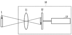
図1は、本発明の撮像装置の概略構成を示した側面図である。撮像素子10は、レンズ光学系11、CCDやCMOS等の光電変換素子を含む撮像素子12、および撮像素子12から出力される光電変換信号を処理して画像信号を生成する信号処理部13を備える。
FIG. 1 is a side view showing a schematic configuration of an imaging apparatus of the present invention. The imaging device 10 includes a lens optical system 11, an imaging device 12 including a photoelectric conversion device such as a CCD or a CMOS, and a signal processing unit 13 that processes a photoelectric conversion signal output from the imaging device 12 to generate an image signal. .
自然光や照明光等の光が物体1に入射し、これを透過/反射/散乱した光は、または、物体1から発する光は、レンズ光学系11により撮像素子12上に光学像を形成する。一般に、レンズ光学系11は、様々な光学収差を補正するため、光軸に沿って並んだ複数のレンズからなるレンズ群により構成されるが、図1では図面を簡略化して単一のレンズとして示している。また、信号処理部13は、生成した画像信号を外部に送出する画像信号出力を備える。
Light such as natural light or illumination light enters the object 1, and light transmitted / reflected / scattered from the object 1 or light emitted from the object 1 forms an optical image on the image sensor 12 by the lens optical system 11. In general, the lens optical system 11 includes a lens group including a plurality of lenses arranged along the optical axis in order to correct various optical aberrations. In FIG. 1, the drawing is simplified to form a single lens. Show. The signal processing unit 13 includes an image signal output for sending the generated image signal to the outside.
なお、本発明の撮像装置10は、赤外光カットの光学フィルタ、電子シャッタ、ビューファインダ、電源(電池)、フラッシュライトなどの公知の構成要素を備え得るが、それらの説明は本発明の理解に特に必要でないため省略する。また、以上の構成はあくまでも一例であり、本発明において、レンズ光学系11、撮像素子12、信号処理部13を除く構成要素には、公知の要素を適切に組み合わせて用いることができる。
The imaging device 10 of the present invention may include known components such as an infrared light cut optical filter, an electronic shutter, a viewfinder, a power source (battery), and a flashlight. It is omitted because it is not necessary. The above configuration is merely an example, and in the present invention, publicly known elements can be appropriately combined and used for the constituent elements other than the lens optical system 11, the image sensor 12, and the signal processing unit 13.
本発明の具体的な実施形態を説明する前に、本発明の実施形態における撮像素子12の概略を説明する。
Before describing a specific embodiment of the present invention, an outline of the image sensor 12 in the embodiment of the present invention will be described.
本発明の実施形態による撮像素子12は、光電変換素子を含むセル(画素)102が2次元状に複数配列された画素アレイと、微小分光素子101が2次元状に複数配列された分光素子アレイとを備える。図2は、本発明の実施形態1に係る撮像素子の画素アレイおよび分光素子アレイの断面の一部を模式的に示す図である。分光素子アレイは画素アレイと対向しており、レンズ光学系からの光が入射する側に配置されている。各微小分光素子101は、厚み一定の複数の柱状構造体で構成されている。なお、微小分光素子101は、便宜上、4本の柱状構造体で表されているが、数や間隔、配列パターンに制限はなく、様々な配列形態をとり得る。
The imaging device 12 according to the embodiment of the present invention includes a pixel array in which a plurality of cells (pixels) 102 including photoelectric conversion elements are arranged in a two-dimensional manner, and a spectroscopic device array in which a plurality of micro-spectral devices 101 are arranged in a two-dimensional manner. With. FIG. 2 is a diagram schematically illustrating a part of a cross section of the pixel array and the spectroscopic element array of the image sensor according to the first embodiment of the present invention. The spectroscopic element array is opposed to the pixel array, and is disposed on the side on which light from the lens optical system is incident. Each microspectral element 101 is composed of a plurality of columnar structures having a constant thickness. Note that the micro-spectral element 101 is represented by four columnar structures for convenience, but the number, interval, and arrangement pattern are not limited, and can take various arrangement forms.
撮像素子12に入射する光に含まれる可視光成分を、波長領域毎に第1の色成分、第2の色成分、第3の色成分に分類する。なお、第1から第3の色成分の組み合わせは、一般に赤(R)、緑(G)、青(B)の3原色の組み合わせであるが、光を3つの波長域に分けるものであればこれに限定されない。
The visible light component included in the light incident on the image sensor 12 is classified into a first color component, a second color component, and a third color component for each wavelength region. The combination of the first to third color components is generally a combination of the three primary colors of red (R), green (G), and blue (B), as long as the light is divided into three wavelength ranges. It is not limited to this.
本発明の実施形態における微小分光素子101は、後述する位相遅延効果およびその構造寸法依存性・波長依存性を利用することで、上述の第1から第3の色成分に応じて、入射した光の伝搬方向を変え、画素アレイ上において空間的に分離する機能を有する。すなわち、本発明の実施形態では、撮像素子に入射した光の少なくとも一部の光が、微小分光素子101によって、色成分に応じて伝搬方向を変え、複数の画素102に入射する。したがって、微小分光素子101と画素102との距離を適切に設定することで、3つの波長域に分離された光を、それぞれ異なった画素102で受けることが可能である。
The micro-spectral element 101 according to the embodiment of the present invention utilizes incident phase light and incident light according to the first to third color components described above by utilizing the phase delay effect and the structural dimension dependency / wavelength dependency described later. Has a function of spatially separating on the pixel array. In other words, in the embodiment of the present invention, at least a part of the light incident on the image sensor changes the propagation direction according to the color component by the micro-spectral element 101 and enters the plurality of pixels 102. Therefore, by appropriately setting the distance between the microspectral element 101 and the pixel 102, the light separated into the three wavelength regions can be received by the different pixels 102, respectively.
画素102に光が入射すると、光電変換素子によって入射した光の強度に応じた電気信号(光電変換信号)を出力するため、色成分に応じた信号(カラー情報)を、直接的に、または信号演算を用いて、取得することができる。以上の微小分光素子101および微小分光素子101に対応した複数の画素102が、2次元状に配置されているため、レンズ光学系11により形成される物体の光学像のカラー情報を取得することができる。
When light enters the pixel 102, an electric signal (photoelectric conversion signal) corresponding to the intensity of the light incident by the photoelectric conversion element is output, so that a signal (color information) corresponding to the color component is directly or signaled. It can be obtained using arithmetic. Since the above-described microspectral element 101 and the plurality of pixels 102 corresponding to the microspectral element 101 are two-dimensionally arranged, it is possible to acquire color information of an optical image of an object formed by the lens optical system 11. it can.
後述する実施形態1および実施形態2については、マイクロレンズアレイを用いることで、入射光のほぼすべてが、分光素子アレイを構成するいずれかの微小分光素子101を透過するため、入射光のほぼすべてが3つの波長域に分離された状態で画素アレイに入射する。したがって、光電変換信号から、直接的に、または簡易な演算をもちいて、カラー情報を取得することができる。
In the first and second embodiments described later, since almost all of the incident light is transmitted through one of the micro-spectral elements 101 constituting the spectroscopic element array by using the microlens array, almost all of the incident light is transmitted. Enters the pixel array in a state of being separated into three wavelength regions. Therefore, color information can be acquired from the photoelectric conversion signal directly or using a simple calculation.
後述する実施形態3および実施形態4については、入射光の一部が、分光素子アレイを構成する微小分光素子101を透過するため、入射光の一部が3つの波長域に分離された状態で画素アレイに入射する。したがって、各画素102の一部は、3つの波長域に分離された状態の光と分離されていない状態の光の合算の光強度に応じた光電変換信号を出力する。出力された光電変換信号に対して、後述する適切な行列演算を用いることで、カラー情報を求めることができる。
In Embodiment 3 and Embodiment 4 to be described later, a part of the incident light is transmitted through the minute spectroscopic element 101 constituting the spectroscopic element array, so that a part of the incident light is separated into three wavelength regions. Incident on the pixel array. Therefore, a part of each pixel 102 outputs a photoelectric conversion signal corresponding to the combined light intensity of the light separated into the three wavelength ranges and the light not separated. Color information can be obtained by using an appropriate matrix operation described later for the output photoelectric conversion signal.
本発明の実施形態における撮像素子12によれば、減色型の色フィルタを用いることなく、微小分光素子101を用いた3色への低損失な光分離により、カラー情報を得ることができる。したがって、色フィルタを用いた撮像素子と比較して、画素アレイに到達する光総量を増加させることができ、撮像感度を高めることが可能となる。さらに、微小分光素子101は作製が簡易な厚み一定の構造体から構成されており、かつ、構造体上面・底面の対称性から偏光依存性が生じないことから、非特許文献1で開示された従来技術における色分離機能に偏光依存性が存在するという課題を解決することができる。
According to the image sensor 12 in the embodiment of the present invention, color information can be obtained by low-loss light separation into three colors using the micro-spectral element 101 without using a subtractive color filter. Therefore, the total amount of light reaching the pixel array can be increased and imaging sensitivity can be increased as compared with an imaging device using a color filter. Further, since the microspectral element 101 is composed of a structure with a uniform thickness that is easy to manufacture and has no polarization dependency due to the symmetry of the top and bottom surfaces of the structure, it is disclosed in Non-Patent Document 1. The problem that the color separation function in the prior art has polarization dependency can be solved.
以下、図面を参照しながら、本発明のより具体的な実施形態を説明する。
Hereinafter, more specific embodiments of the present invention will be described with reference to the drawings.
(実施形態1)
以下、本実施形態1における撮像素子の構成の概略について説明する。 (Embodiment 1)
Hereinafter, an outline of the configuration of the image sensor according to the first embodiment will be described.
以下、本実施形態1における撮像素子の構成の概略について説明する。 (Embodiment 1)
Hereinafter, an outline of the configuration of the image sensor according to the first embodiment will be described.
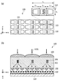
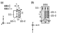
図3(a)は、本発明の実施形態1に係る撮像素子の一部の概略構成の上面図であり、図3(b)はその断面図である。本実施形態1における撮像素子100は、光電変換素子を含む画素102がアレイ状になるように配列された2次元画素アレイ上に、SiO2等からなる低屈折率の透明層111、複数のマイクロレンズ103が積層されている。低屈折率の透明層111の内部には、透明層111の屈折率よりも高い屈折率を有するSiN等の材料から形成された複数の厚み(2次元画素アレイに対して垂直方向の長さ)一定の微細構造体からなる微小分光素子101が埋め込まれている。便宜上、以下の説明において、2次元画素アレイの法線方向をz軸、2次元画素アレイに平行で、画素ユニット110を構成する3つの画素102が並ぶ方向をx軸、2次元画素アレイに平行でx軸と直交する方向をy軸とするxyz直交座標系を設定する。
FIG. 3A is a top view of a schematic configuration of a part of the image sensor according to the first embodiment of the present invention, and FIG. 3B is a cross-sectional view thereof. The imaging device 100 according to the first embodiment includes a low-refractive-index transparent layer 111 made of SiO 2 or the like on a two-dimensional pixel array in which pixels 102 including photoelectric conversion elements are arranged in an array, and a plurality of microarrays. A lens 103 is stacked. A plurality of thicknesses (length in the direction perpendicular to the two-dimensional pixel array) formed of a material such as SiN having a refractive index higher than the refractive index of the transparent layer 111 inside the low refractive index transparent layer 111 A microspectral element 101 made of a certain fine structure is embedded. For convenience, in the following description, the normal direction of the two-dimensional pixel array is parallel to the z-axis and the two-dimensional pixel array, and the direction in which the three pixels 102 constituting the pixel unit 110 are aligned is parallel to the x-axis and the two-dimensional pixel array. To set an xyz orthogonal coordinate system in which the direction orthogonal to the x axis is the y axis.
図に示されているように、マイクロレンズ103、微小光学素子101、画素102はxy平面上において格子状に配置されており、各マイクロレンズ103の中心軸上に1つの微小分光素子102が配置されている。x軸方向に隣り合う3つの画素を1つの画素ユニット110とすると、x軸方向に隣り合う各マイクロレンズ103はそれぞれ画素ユニット110と一対一で対応し、各マイクロレンズ103の中心軸は対応する画素ユニットの中央の画素102のほぼ中心を通過する。すなわち、x軸方向に隣り合う3つの画素102に対して1つのマイクロレンズ103および1つの微小分光素子101が対応しており、上記のマイクロレンズ103、微小分光素子101、画素ユニット110を1つの撮像素子ユニットとすると、その撮像素子ユニットがxy平面上において格子状に配列されている。
As shown in the figure, the micro lens 103, the micro optical element 101, and the pixel 102 are arranged in a lattice shape on the xy plane, and one micro spectroscopic element 102 is arranged on the central axis of each micro lens 103. Has been. When three pixels adjacent in the x-axis direction are defined as one pixel unit 110, each microlens 103 adjacent in the x-axis direction has a one-to-one correspondence with the pixel unit 110, and the central axis of each microlens 103 corresponds. It passes almost the center of the pixel 102 at the center of the pixel unit. That is, one microlens 103 and one microspectral element 101 correspond to three pixels 102 adjacent in the x-axis direction, and the above-described microlens 103, microspectral element 101, and pixel unit 110 are combined into one pixel. Assuming that the imaging element unit is used, the imaging element units are arranged in a lattice pattern on the xy plane.
なお、上述の説明では、一例として、直交格子状に配列された2次元画素アレイの場合について説明したが、画素102の配列、形状、サイズなどはこの図の例に限られず、公知のどのような配列、形状、サイズであってもよい。また、図3(a)、(b)では省略しているが、2次元画素アレイと微細構造体との間に、内部マイクロレンズとして動作し、微小分光素子101からの光を画素102内の光電変換素子へと導く働きをなすSiN等からなる高屈折率の凹凸構造を備え得る。図3(a)、(b)に示される構造は、公知の半導体製造技術により作製され得る。
In the above description, the case of a two-dimensional pixel array arranged in an orthogonal grid is described as an example. However, the arrangement, shape, size, and the like of the pixels 102 are not limited to the example in this figure, and any known method Any arrangement, shape and size may be used. Although not shown in FIGS. 3A and 3B, it operates as an internal microlens between the two-dimensional pixel array and the fine structure, and the light from the microspectral element 101 is transmitted in the pixel 102. A concavo-convex structure with a high refractive index made of SiN or the like that functions to lead to a photoelectric conversion element can be provided. The structure shown in FIGS. 3A and 3B can be manufactured by a known semiconductor manufacturing technique.
なお、図3(a)、(b)に示される撮像素子100は、は、配線層112の反対側から受光する裏面照射型の構造であるが、本実施形態ではこのような構造に限定されず、配線層112の側から受光する表面照射型の構造を有していてもよい。
3A and 3B has a back-illuminated structure in which light is received from the opposite side of the wiring layer 112. However, in the present embodiment, the imaging element 100 is limited to such a structure. Instead, it may have a surface irradiation type structure that receives light from the wiring layer 112 side.
以下、本実施形態における撮像素子100の各構成要素の働きについて説明する。
Hereinafter, the function of each component of the image sensor 100 in the present embodiment will be described.
撮像素子100に入射する白色の光は、まずマイクロレンズアレイによって集光され、ほぼすべての光が各マイクロレンズ103に対応した微小分光素子101を通過する。各微小分光素子101によって、光はxz面内で3波長域に空間的に分離され、各微小分光素子101の直下にある3画素102によりそれぞれ受光される。図3(b)に示す例では、各微小分光素子101によって、第1色成分の光(R)が第1の方向(右)へ、第2色成分の光(G)が第2の方向(直進)へ、第3色成分の光(B)が第3の方向(左)へ伝搬しているため、各微小分光素子101直下の3画素102DR(右)、DG(中央)、DB(左)がそれぞれR、G、Bのカラー情報の検出に対応する。
The white light incident on the image sensor 100 is first condensed by the microlens array, and almost all the light passes through the microspectral element 101 corresponding to each microlens 103. The light is spatially separated into three wavelength regions in the xz plane by each microspectral element 101 and received by the three pixels 102 immediately below each microspectral element 101. In the example shown in FIG. 3B, the light (R) of the first color component goes in the first direction (right) and the light (G) of the second color component goes in the second direction by each micro-spectral element 101. Since the light (B) of the third color component is propagating in the third direction (left), the three pixels 102D R (right), D G (center), D B (left) corresponds to detection of R, G, and B color information, respectively.
なお、上述は一例であって、各微小分光素子101の構成によっては、色成分と伝搬方向の組み合わせは自由に変更可能であり、それに伴って、RGBそれぞれに対応する画素102DR、DG、DBも変更される。
Note that the above is an example, and depending on the configuration of each micro-spectral element 101, the combination of the color component and the propagation direction can be freely changed, and accordingly, the pixels 102D R , D G , D B is also changed.
このように3波長域に空間的に分離された光が3画素102によりそれぞれ受光されると、各画素102内の光電変換素子によって光電変換がなされ、カラー情報を含む画像信号が出力される。
When the light spatially separated into the three wavelength regions is received by the three pixels 102 as described above, photoelectric conversion is performed by the photoelectric conversion element in each pixel 102, and an image signal including color information is output.
なお、各微小分光素子101の直下にある3画素102DR、DG、DBのx軸方向の幅wd1、wd2、wd3は、同一であっても異なっていても良い。また、これに伴って、マイクロレンズ103のx軸方向の幅wlxとy軸方向の幅wlyは同一であっても異なっていても良い。図3の例では、3画素102DR、DG、DBのx軸方向の幅wd1、wd2、wd3が同一であり、マイクロレンズ103はwlxとwlyは異なっている。
Note that the widths w d1 , w d2 , and w d3 in the x-axis direction of the three pixels 102D R , D G , and D B immediately below each microspectral element 101 may be the same or different. Accordingly, the width w lx in the x-axis direction and the width w ly in the y-axis direction of the microlens 103 may be the same or different. In the example of FIG. 3, the widths w d1 , w d2 , and w d3 in the x-axis direction of the three pixels 102D R , D G , and D B are the same, and w lx and w ly of the microlens 103 are different.
また、画素ユニット110と微小分光素子101との間には、内部マイクロレンズとして動作するSiN等からなる高屈折率の凹凸構造を備え得るが、後述する微小分光素子101は形成する位相遅延分布によっては、レンズ機能を有することが可能であるため、内部マイクロレンズを省略することも可能である。
In addition, a concavo-convex structure with a high refractive index made of SiN or the like that operates as an internal microlens can be provided between the pixel unit 110 and the microspectral element 101, but the microspectral element 101 described later depends on a phase delay distribution to be formed. Since it can have a lens function, the internal microlens can be omitted.
以下、本実施形態における微小分光素子について説明する。
Hereinafter, the microspectral element in the present embodiment will be described.
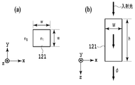
本実施形態1における微小分光素子101は、複数の微細な柱状構造体121から構成される。図4(a)は、本発明の実施形態1に係る撮像素子の微小分光素子を構成する柱状構造体の上面図であり、図4(b)は、その断面図である。柱状構造体121は、透明層111の屈折率n0よりも高い屈折率n1を有するSiN等の材料から形成されており、構造の厚みhは一定である。
The microspectral element 101 according to the first embodiment includes a plurality of fine columnar structures 121. FIG. 4A is a top view of a columnar structure constituting the microspectral element of the image sensor according to Embodiment 1 of the present invention, and FIG. 4B is a cross-sectional view thereof. The columnar structure 121 is made of a material such as SiN having a refractive index n 1 higher than the refractive index n 0 of the transparent layer 111, and the thickness h of the structure is constant.
また、柱状構造体121の底面および上面は正方形である。この柱状構造体121は、透明層111との屈折率差から、光を構造内に閉じ込めて伝搬させる光導波路として機能する。したがって、上面側から光を入射すると、光は柱状構造体121内に強く閉じ込められながら伝搬し、光導波路の実効的な屈折率neffにより決定される位相遅延効果を受けて、底面側から出力される。具体的に、透明層111を柱状構造体121の厚み分の長さを伝搬した光の位相を基準とした際、柱状構造体121による位相遅延量φは、光の真空中での波長をλとおくと、
φ=(neff-n0)×2πh/λ (1)
で表わされる。この位相遅延量は光の波長λによって異なるため、同一の柱状構造体121に入射した光に対して波長域(色成分)に応じて異なる位相遅延量を与えることができる。また、柱状構造体121の底面および上面が正方形であるため、偏光方向を変化させた場合においても、位相遅延効果を含む光学特性に変化はない。さらに、neffは構造寸法の関数であることが知られており、n0<neff<n1の値をとる。したがって、図4(a)、(b)に示す例では、柱状構造体121の幅wを変化させることで、任意の位相遅延量を設定することが可能である。 Further, the bottom surface and the top surface of thecolumnar structure 121 are square. This columnar structure 121 functions as an optical waveguide for confining and propagating light in the structure from the difference in refractive index with the transparent layer 111. Therefore, when light is incident from the upper surface side, the light propagates while being strongly confined in the columnar structure 121, receives the phase delay effect determined by the effective refractive index n eff of the optical waveguide, and is output from the lower surface side. Is done. Specifically, when the phase of light propagating through the length of the thickness of the columnar structure 121 through the transparent layer 111 is used as a reference, the phase delay amount φ by the columnar structure 121 is the wavelength of light in vacuum λ. After all,
φ = (n eff −n 0 ) × 2πh / λ (1)
It is represented by Since this phase delay amount differs depending on the light wavelength λ, different phase delay amounts can be given to the light incident on the samecolumnar structure 121 according to the wavelength region (color component). Further, since the bottom surface and the top surface of the columnar structure 121 are square, even when the polarization direction is changed, the optical characteristics including the phase delay effect are not changed. Furthermore, n eff is known to be a function of structural dimensions and takes a value of n 0 <n eff <n 1 . Therefore, in the example shown in FIGS. 4A and 4B, it is possible to set an arbitrary amount of phase delay by changing the width w of the columnar structure 121.
φ=(neff-n0)×2πh/λ (1)
で表わされる。この位相遅延量は光の波長λによって異なるため、同一の柱状構造体121に入射した光に対して波長域(色成分)に応じて異なる位相遅延量を与えることができる。また、柱状構造体121の底面および上面が正方形であるため、偏光方向を変化させた場合においても、位相遅延効果を含む光学特性に変化はない。さらに、neffは構造寸法の関数であることが知られており、n0<neff<n1の値をとる。したがって、図4(a)、(b)に示す例では、柱状構造体121の幅wを変化させることで、任意の位相遅延量を設定することが可能である。 Further, the bottom surface and the top surface of the
φ = (n eff −n 0 ) × 2πh / λ (1)
It is represented by Since this phase delay amount differs depending on the light wavelength λ, different phase delay amounts can be given to the light incident on the same
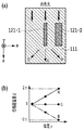
図5(a)の断面図は、x軸方向に上述の柱状構造体121-1、121-2を2つ並べて構成した、本実施形態1における微小分光素子101の一例である。なお、y軸方向には、波長以下の間隔で、上述の柱状構造体121-1、121-2が複数並んでいる。
The cross-sectional view of FIG. 5A is an example of the microspectral element 101 according to the first embodiment, in which the two columnar structures 121-1 and 121-2 are arranged in the x-axis direction. In the y-axis direction, a plurality of the columnar structures 121-1 and 121-2 are arranged at intervals equal to or shorter than the wavelength.
図5(a)に示すように、x軸方向に隣接する柱状構造体121-1、121-2の幅wが異なっている。この幅wの差異により、微小分光素子101を透過した光に対して、波長領域毎に異なる位相遅延分布を与えることが可能となり、光波面を変化させることができる。光の伝搬方向(偏向方向)はこの光波面によって決定されるため、微小分光素子101を透過した光を波長域(色成分)に応じて空間的に分離することが可能となる。すなわち、本実施形態1における微小分光素子101は、複数の柱状構造体121を配置し、隣接する柱状構造体121-1、121-2の光の伝搬方向と直交する面における寸法wを変化させることで、入射光の波長領域に応じて異なる光波面を与え、色成分を空間的に分離する。
As shown in FIG. 5A, the widths w of the columnar structures 121-1 and 121-2 adjacent in the x-axis direction are different. Due to the difference in the width w, it becomes possible to give different phase delay distributions for each wavelength region to the light transmitted through the microspectral element 101, and the light wavefront can be changed. Since the light propagation direction (deflection direction) is determined by this light wavefront, it is possible to spatially separate the light transmitted through the micro-spectral element 101 according to the wavelength range (color component). That is, in the microspectral element 101 according to the first embodiment, a plurality of columnar structures 121 are arranged, and the dimension w on the plane orthogonal to the light propagation direction of the adjacent columnar structures 121-1 and 121-2 is changed. Thus, different light wavefronts are given according to the wavelength region of the incident light, and the color components are spatially separated.
例えば、図5(a)に示す構造の場合、図5(b)に示すように、3波長(例えば、RGBに対応する波長)に応じて異なる位相遅延分布を与えることができる。この例では、第1色成分の光(R)に対応する波長の位相遅延分布は位相量が0から+2πまで線形増加する直線上に沿っており、第2色成分の光(G)に対応する波長の位相遅延分布は空間的な変化はなく、第3色成分の光(B)に対応する波長の位相遅延分布は位相量が0から-2πまで線形減少する直線上に沿っている。この場合、微小分光素子101を透過した光は、図5(a)に示すように、第1色成分の光(R)が第1の方向(右)へ、第2色成分の光(G)が第2の方向(直進)へ、第3色成分の光(B)が第3の方向(左)へそれぞれ効率よく伝搬することができる。
For example, in the case of the structure shown in FIG. 5A, different phase delay distributions can be given according to three wavelengths (for example, wavelengths corresponding to RGB) as shown in FIG. 5B. In this example, the phase delay distribution of the wavelength corresponding to the light (R) of the first color component is along a straight line in which the phase amount linearly increases from 0 to + 2π, and corresponds to the light (G) of the second color component. There is no spatial change in the phase delay distribution of the wavelength to be transmitted, and the phase delay distribution of the wavelength corresponding to the light (B) of the third color component is along a straight line in which the phase amount linearly decreases from 0 to −2π. In this case, as shown in FIG. 5A, the light transmitted through the micro-spectral element 101 is the first color component light (R) in the first direction (right) and the second color component light (G ) In the second direction (straight), and the light (B) of the third color component can be efficiently propagated in the third direction (left).
なお、上述の説明は一例であって、各柱状構造体121の寸法によっては、色成分と偏向方向の組み合わせは自由に変更可能である。例えば、第1色成分の光(R)が第2の方向(直進)へ、第2色成分の光(G)が第1の方向(右)へ、第3色成分の光(B)が第3の方向(左)へそれぞれ効率よく伝搬することができる。
The above description is an example, and the combination of the color component and the deflection direction can be freely changed depending on the dimensions of each columnar structure 121. For example, the first color component light (R) travels in the second direction (straight), the second color component light (G) travels in the first direction (right), and the third color component light (B) travels. Each can propagate efficiently in the third direction (left).
本実施形態における微小分光素子101のより詳細な一例を説明する。
A more detailed example of the microspectral element 101 in this embodiment will be described.
図6(a)は、本発明の実施形態1に係る撮像素子の微小分光素子の一例の上面図であり、図6(b)は、その断面図である。x軸方向には互い異なる幅w1、w2をもつ厚さ(2次元画素アレイに対して垂直方向の長さ)が一定の柱状構造体121-1、121-2が2つ並んでおり、y軸方向には同じ柱状構造体121-1、121-2が3つ並んでおり、以上を1つの微小分光素子101とする。なお、柱状構造体121-1、121-2を構成する材料はSiN(n1=2.03)を想定し、透明層を構成する材料はSiO2(n0=1.45)を想定し、底面および上面が正方形の場合を示している。また、すべての柱状構造体121-1、121-2の厚みhを1200nm、パターン左側の柱状構造体121-1の幅w1を145nm、パターン右側の柱状構造体121-2の幅w2を340nmとし、x軸およびy軸方向のおける柱状構造体121-1、121-2の間隔pは450nmとした。
FIG. 6A is a top view of an example of the microspectral element of the imaging element according to Embodiment 1 of the present invention, and FIG. 6B is a cross-sectional view thereof. Two columnar structures 121-1 and 121-2 are arranged in the x-axis direction, with different widths w 1 and w 2 (thickness in the direction perpendicular to the two-dimensional pixel array). The three columnar structures 121-1 and 121-2 are arranged in the y-axis direction, and the above is referred to as one micro-spectral element 101. The material constituting the columnar structures 121-1 and 121-2 is assumed to be SiN (n 1 = 2.03), and the material constituting the transparent layer is assumed to be SiO 2 (n 0 = 1.45). The bottom and top surfaces are square. Also, all of the thickness h of the columnar structure 121-1 and 121-2 1200 nm, 145 nm width w 1 of the pattern left columnar structure 121-1, the width w 2 of the pattern right columnar structure 121-2 The distance p between the columnar structures 121-1 and 121-2 in the x-axis and y-axis directions was 450 nm.
図7(a)、(b)に、上述の構造において、柱状構造体121-1、121-2の上面から平行光を入射した際、微小分光素子101の出射端から3方向(図6(b)のR、G、Bの各方向)に分離して伝搬する効率(入射光強度に対する各伝搬方向の光強度の比)の波長依存性(厳密結合波理論に基づく計算結果)を示す。図7(a)は、図6(a)中の縦の偏光をもつ光、図7(b)は図6(a)中の横の偏光をもつ光をそれぞれ入射した際の結果である。なお、計算の際、上述の微小分光素子101がx軸およびy軸方向においてPの間隔(P=3p)で並んでいると仮定したが、単体の微小分光素子101における光学機能との差異はほとんどないことを確認している。また、3方向のそれぞれの偏向角θR、θG、θBは、光の回折に基づいており、R:sinθR=λ/P、G:θG=0(直進)、B:sinθB=λ/Pとした。
7A and 7B, in the above-described structure, when parallel light is incident from the upper surfaces of the columnar structures 121-1 and 121-2, three directions from the emission end of the microspectral element 101 (FIG. 6 ( b) shows the wavelength dependence (calculation result based on the strict coupled wave theory) of the efficiency (ratio of the light intensity in each propagation direction with respect to the incident light intensity) that propagates separately in the R, G, and B directions). FIG. 7A shows a result when light having a vertically polarized light in FIG. 6A is incident, and FIG. 7B shows a result when light having a horizontally polarized light in FIG. 6A is incident. In the calculation, it is assumed that the above-described micro-spectral elements 101 are arranged at intervals of P (P = 3p) in the x-axis and y-axis directions, but the difference from the optical function of the single micro-spectral element 101 is as follows. It is confirmed that there is almost no. The deflection angles θ R , θ G , and θ B in the three directions are based on light diffraction, and R: sin θ R = λ / P, G: θ G = 0 (straight), and B: sin θ B = Λ / P.
また、図7(a)、(b)に示した特性は、従来の撮像装置における色フィルタの分光感度特性に相当する。図7(a)、(b)に示す結果は、第1の方向(R)における効率は600nm以上の赤色波長域でピークをなし、第2の方向(G)における効率は500-600nmの緑色波長域でピークをなし、第3の方向(B)における効率は500nm以下の青色波長域でピークをなしていることを示している。また、40~60%という良好な分光性能を示しており、かつ特性に大きな偏光依存性はみられない。なお、曲線R、G、Bの総和、すなわち総透過率は、95%以上であり、散乱や反射による光損失はほとんど生じない。
Further, the characteristics shown in FIGS. 7A and 7B correspond to the spectral sensitivity characteristics of the color filter in the conventional imaging apparatus. The results shown in FIGS. 7A and 7B show that the efficiency in the first direction (R) peaks in the red wavelength region of 600 nm or more, and the efficiency in the second direction (G) is 500-600 nm green. It shows a peak in the wavelength range, and the efficiency in the third direction (B) shows a peak in the blue wavelength range of 500 nm or less. Further, it exhibits a good spectral performance of 40 to 60%, and no significant polarization dependence is seen in the characteristics. Note that the sum of the curves R, G, and B, that is, the total transmittance is 95% or more, and light loss due to scattering and reflection hardly occurs.
以上の結果は、本実施形態1における微小分光素子101を用いることで、色成分の高効率な空間的な分離が可能であることを示している。さらに、上述の例では、単体の微小分光素子101のサイズは1.35μm角であり、一般的なCCDおよびCMOSセンサの最小ピクセルサイズと同等である。したがって、最小ピクセルサイズをもつ画素ユニット110に対応した微小分光素子101の形成が可能である。なお、柱状構造体121のサイズや数、配列パターンによって、異なるサイズの微小分光素子101を形成することも可能である。
The above results indicate that the use of the microspectral element 101 according to the first embodiment enables highly efficient spatial separation of color components. Furthermore, in the above example, the size of the single micro-spectral element 101 is 1.35 μm square, which is equivalent to the minimum pixel size of general CCD and CMOS sensors. Therefore, it is possible to form the microspectral element 101 corresponding to the pixel unit 110 having the minimum pixel size. Note that the micro-spectral elements 101 having different sizes can be formed depending on the size, number, and arrangement pattern of the columnar structures 121.
微小分光素子101を構成する柱状構造体121の材料、数、形状、サイズ、配列パターンなどを適切に設計することにより、所望の分光特性を与えることが可能である。その結果、上述したように、個々の光電変換素子に所望の波長域の光のみを分離して入射させることが可能となり、各光電変換素子から出力される光電変換信号から、色成分に対応する信号を取得することができる。
It is possible to give desired spectral characteristics by appropriately designing the material, number, shape, size, arrangement pattern, and the like of the columnar structures 121 constituting the microspectral element 101. As a result, as described above, it is possible to separate and enter only light in a desired wavelength range into each photoelectric conversion element, and correspond to color components from the photoelectric conversion signals output from each photoelectric conversion element. A signal can be acquired.
また、上述の通り、微小分光素子101による光損失はほとんど生じないため、従来技術の色フィルタを用いた撮像素子と比較して、画素アレイに到達する光総量を飛躍的に増加させることができ、撮像感度を高めることが可能となる。なお、各微小分光素子101の分光性能が上述した理想的な性能と多少異なっていても、性能の差異の程度に応じて、取得した信号を補正・演算することによって良好な色情報を得ることが可能である。
Further, as described above, since the optical loss due to the micro-spectral element 101 hardly occurs, the total amount of light reaching the pixel array can be drastically increased as compared with the imaging element using the conventional color filter. The imaging sensitivity can be increased. Even if the spectral performance of each microspectral element 101 is slightly different from the ideal performance described above, good color information can be obtained by correcting and calculating the acquired signal according to the degree of the difference in performance. Is possible.
また、上述の各柱状構造体121の配置において、周期的な構造に起因する不要な回折光が発生することを防ぐため、光の波長以下の間隔で配置することが望ましい。
Also, in the arrangement of the columnar structures 121 described above, it is desirable to arrange them at intervals equal to or less than the wavelength of the light in order to prevent unnecessary diffracted light from being generated due to the periodic structure.
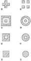
上述の例では、柱状構造体の底面および上面が正方形の場合について説明したが、この形状に限定されない。すなわち、底面および上面の中心を通る軸を対称軸として4回回転対称となる形状面であれば、分光機能の偏光に対する依存性が生じることはなく、位相遅延効果をもたらす光導波路としての動作も失われることはない。したがって、図8(a)~(h)に示すような正方形、中空正方形、円形、中空円形、十字形状といった4回回転対称となる面をもつ柱状構造体を採用することが望ましい。
In the above example, the case where the bottom surface and the top surface of the columnar structure are square has been described, but the present invention is not limited to this shape. That is, if the shape surface has a four-fold rotational symmetry with the axis passing through the center of the bottom surface and the top surface as the symmetry axis, the dependence of the spectral function on the polarization does not occur, and the operation as an optical waveguide that provides the phase delay effect There is no loss. Therefore, it is desirable to employ a columnar structure having a four-fold rotational symmetry such as a square, a hollow square, a circle, a hollow circle, and a cross shape as shown in FIGS.
なお、微小分光素子101による色成分の分離後において、画素ユニット110上の各光空間分布が互いに十分に分離するためには、微小分光素子101の出力端と画素102の光電変換素子との間が1μm以上の間隔であることが好ましい。一方で、撮像素子100の薄膜化および材料費・プロセス時間の節約のため、上述の微小分光素子101の出力端と画素102の光電変換素子との間隔は、可能な限り短い方が好ましい。
In addition, after the color components are separated by the micro-spectral element 101, in order for the respective light spatial distributions on the pixel unit 110 to be sufficiently separated from each other, between the output end of the micro-spectral element 101 and the photoelectric conversion element of the pixel 102. Is preferably 1 μm or more. On the other hand, in order to reduce the thickness of the image sensor 100 and save material costs and process time, it is preferable that the interval between the output end of the microspectral element 101 and the photoelectric conversion element of the pixel 102 be as short as possible.
また、この場合、短い伝搬距離で、画素ユニット110上の各光空間分布が色成分に応じて互いにはっきり分離する必要があるため、微小分光素子101によって光の波面を大きく傾けて、偏向する(曲がる)角度を大きくすることが好ましい。偏向する角度を大きくするには、微小分光素子101により形成される各波長域における位相遅延分布がそれぞれ0から2πまで変化する形が適しているため、それぞれの波長域において、柱状構造体121による位相遅延量の可変範囲は、2π以上有していることが好ましい。したがって、式(1)から、分離する波長域の最も長波長側の波長域における所望の中心波長をλrとすると、柱状構造体121の厚みhは、h=λr/(n1-n0)の近傍に設定することが望ましい。
Further, in this case, since each light spatial distribution on the pixel unit 110 needs to be clearly separated from each other according to the color component with a short propagation distance, the microscopic spectroscopic element 101 deflects the wavefront of the light by being greatly inclined ( It is preferable to increase the angle. In order to increase the deflection angle, it is suitable that the phase delay distribution in each wavelength region formed by the micro-spectral element 101 changes from 0 to 2π, so that the columnar structure 121 is used in each wavelength region. The variable range of the phase delay amount is preferably 2π or more. Therefore, from Equation (1), if the desired center wavelength in the wavelength range on the longest wavelength side of the wavelength range to be separated is λ r , the thickness h of the columnar structure 121 is h = λ r / (n 1 −n It is desirable to set it in the vicinity of 0 ).
以上のような分光機能をもつ微小分光素子101は、公知の半導体製造技術により、薄膜堆積およびパターニングを実行することにより作製することができる。本実施形態1の微小分光素子101は、複数の厚さ一定の柱状構造体121から構成されるため、非特許文献1で開示されている階段状構造等と比較して、安価で容易に作製できる。
The micro-spectral element 101 having the spectral function as described above can be manufactured by performing thin film deposition and patterning by a known semiconductor manufacturing technique. Since the microspectral element 101 according to the first embodiment includes a plurality of columnar structures 121 having a constant thickness, the microspectral element 101 can be easily manufactured at a lower cost than the stepped structure disclosed in Non-Patent Document 1. it can.
以下、本実施形態の撮像素子のおける微小光学素子および画素の配置について説明する。
Hereinafter, the arrangement of micro optical elements and pixels in the image sensor of the present embodiment will be described.
図3に示した一例では、x軸方向に沿って配置された微小分光素子101の行が、x軸方向にずれることなくy軸方向に沿って繰り返し配置されており、その結果y軸方向に沿って微小分光素子101のパターンが連続的に配置されている。この場合、x軸方向においては、各微小分光素子101直下の色成分に対応する3画素102DB、DG、DRが左からこの順に並び、この並びが繰り返して配置されている。
In the example shown in FIG. 3, the rows of micro-spectral elements 101 arranged along the x-axis direction are repeatedly arranged along the y-axis direction without shifting in the x-axis direction, and as a result, in the y-axis direction. A pattern of the microspectral element 101 is continuously arranged along the line. In this case, in the x-axis direction, the three pixels 102D B , D G , and D R corresponding to the color components immediately below each micro-spectral element 101 are arranged in this order from the left, and this arrangement is repeatedly arranged.
さらに、画素102についても同様に、x軸方向に沿って配置された画素102の行が、x軸方向にずれることなくy軸方向に沿って繰り返し配置されており、その結果y軸方向に沿って3画素102DB、DG、DRがそれぞれ連続的に配置されている。
Further, similarly for the pixels 102, the rows of the pixels 102 arranged along the x-axis direction are repeatedly arranged along the y-axis direction without shifting in the x-axis direction, and as a result, along the y-axis direction. Thus, the three pixels 102D B , D G , and D R are continuously arranged.
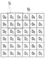
図9(a)~(c)は、本発明の実施形態1に係る撮像素子の色成分に対応する画素の配置を模式的に表したものである。x軸方向に隣り合う3つの画素102DB、DG、DRを1つのカラー画素ユニットUとすると、図9(a)に示すカラー画素ユニットU1、および、カラー画素ユニットU1に対して単一画素だけx軸方向にシフトしたカラー画素ユニットU2は、どちらもR、G、Bに対応する画素を必ず1つずつ含むことになる。すなわち、カラー画素ユニットUをxy平面において単一画素ずつシフトしながら、カラー情報取得すれば、RGB3色の情報をほぼ画素数分だけ得ることができる。このことは、撮像素子の解像度を画素数の程度まで高めることができることを意味している(いわゆるベイヤー配置と同等である)。したがって、本実施形態1の撮像素子は、高感度であることに加えて、単一画素サイズの高解像度でカラー情報を生成することができる。
FIGS. 9A to 9C schematically show the arrangement of pixels corresponding to the color components of the image sensor according to the first embodiment of the present invention. Assuming that the three pixels 102D B , D G , and D R adjacent in the x-axis direction are one color pixel unit U, the color pixel unit U 1 and the color pixel unit U 1 shown in FIG. The color pixel unit U 2 shifted by a single pixel in the x-axis direction always includes one pixel corresponding to each of R, G, and B. That is, if the color information is acquired while shifting the color pixel unit U by a single pixel in the xy plane, information of RGB three colors can be obtained by the number of pixels. This means that the resolution of the image sensor can be increased to the number of pixels (equivalent to a so-called Bayer arrangement). Therefore, in addition to high sensitivity, the image sensor of the first embodiment can generate color information with high resolution of a single pixel size.
上述のような単一画素サイズの解像度を実現する微小光学素子および画素の配置は、図9(a)に限定されず、種々に変更することができる。図9(b)および図9(c)は、別の例を示しており、x軸方向沿って構成される微小分光素子101およびカラー画素ユニットUの行が、図9(b)では1画素サイズ分、図9(c)では2画素サイズ分、x軸方向にシフトしながら、順次y軸方向に配置されている。このような配置についても、図9(a)と同様に単一画素サイズの解像度でカラー情報を生成することができる。
The arrangement of the micro optical elements and the pixels that realize the resolution of the single pixel size as described above is not limited to FIG. 9A and can be variously changed. FIG. 9B and FIG. 9C show another example, and the row of the micro-spectral element 101 and the color pixel unit U configured along the x-axis direction is one pixel in FIG. 9B. In FIG. 9C, the pixels are sequentially arranged in the y-axis direction while shifting in the x-axis direction by the size of two pixels in FIG. With such an arrangement, color information can be generated with a resolution of a single pixel size as in FIG. 9A.
図10(a)~(c)は、図9(a)~(c)とは別の配置の例を示しており、行毎に3画素DB、DG、DRの順番が反転する構成であり、x軸方向にシフトについては上述の図9(a)~(c)とそれぞれ同様である。この場合についても、図9(a)と同様に単一画素サイズの解像度でカラー情報を生成することができる。なお、3画素DB、DG、DRの順番の反転を行うには、上述の微小分光素子101の柱状構造体121-1、121-2を、x軸において、左右反転させたパターンを用いればよい。
Figure 10 (a) ~ (c) shows an example of another arrangement from FIG 9 (a) ~ (c) , 3 pixels D B for each row, D G, the order of D R inverts The shift in the x-axis direction is the same as that in FIGS. 9A to 9C described above. Also in this case, color information can be generated with a resolution of a single pixel size as in FIG. In order to reverse the order of the three pixels D B , D G , and D R , a pattern obtained by horizontally reversing the columnar structures 121-1 and 121-2 of the above-described microspectral element 101 on the x axis is used. Use it.
上述した図9(a)~(c)および図10(a)~(c)に示す画素配置は、入射光が各微小分光素子101の機能によって、第1色成分の光(R)が第1の方向(右)へ、第2色成分の光(G)が第2の方向(直進)へ、第3色成分の光(B)が第3の方向(左)へ伝搬し、各微小分光素子101直下の3画素102DR(右)、DG(中央)、DB(左)がそれぞれR、G、Bのカラー情報の検出に対応すると想定した際のものである。上述したように、微小分光素子101の構成によっては、微小分光素子101直下の画素102がRGB3色のいずれに対応したものになるか変わるが、基本的にはカラー画素ユニットU内の順番が変更されるだけである。そのような場合についても、図9および図10に示したカラー画素ユニットUの配置規則に従って、配置を設定すれば、同様に単一画素サイズの解像度でカラー情報を生成することができる。
In the pixel arrangements shown in FIGS. 9A to 9C and FIGS. 10A to 10C described above, the incident light is affected by the function of each microspectral element 101, and the first color component light (R) is the first. In the direction 1 (right), the second color component light (G) propagates in the second direction (straight), and the third color component light (B) propagates in the third direction (left). This is based on the assumption that the three pixels 102D R (right), D G (center), and D B (left) immediately below the spectroscopic element 101 correspond to detection of R, G, and B color information, respectively. As described above, depending on the configuration of the microspectral element 101, the pixel 102 immediately below the microspectral element 101 corresponds to which of the three colors RGB, but basically the order in the color pixel unit U is changed. It is only done. Even in such a case, if the arrangement is set according to the arrangement rule of the color pixel unit U shown in FIGS. 9 and 10, the color information can be similarly generated with the resolution of the single pixel size.
以上の説明では、微小分光素子101のみを用いた場合の撮像素子100について述べた。次に、減色型の色フィルタを併用した際の変形例について説明する。
In the above description, the imaging device 100 when only the micro-spectral element 101 is used has been described. Next, a modified example when a subtractive color filter is used in combination will be described.
図11に、本発明の実施形態1の変形例である撮像素子の概略構成の断面図を示す。図3との差異は、色成分に対応した画素102の上方に、画素102の色にそれぞれ対応した色フィルタ104を配置している点であり、その他は同一である。この構成の場合、従来技術の色フィルタのみの構成に比べて、光利用効率が向上し、かつ色再現性も向上する。
FIG. 11 is a cross-sectional view of a schematic configuration of an image sensor that is a modification of the first embodiment of the present invention. The difference from FIG. 3 is that a color filter 104 corresponding to each color of the pixel 102 is arranged above the pixel 102 corresponding to the color component, and the others are the same. In the case of this configuration, the light utilization efficiency is improved and the color reproducibility is improved as compared with the configuration of only the conventional color filter.
例えば、図7より、微小分光素子101のRGBへの分光効率は40~60%とする。また、RGBの色フィルタ104の対応する波長域における透過率(分光効率)をそれぞれ90%とする。入射光がRGB1:1:1の比率の強度を有しているとする。この場合、微小分光素子101と色フィルタ104を併用した構成では、光が両者を透過して画素に入射するため、RGB3画素102に到達する光強度の総量は36~54%となる。さらに、微小分光素子101および色フィルタ104の分光性能が掛け合わされ、不要な色成分が排除された状態で各画素102に入射するため、色再現性が大きく向上する。一方、色フィルタ104のみの構成の場合、3画素102に到達する光強度の総量は30%となり、色再現性も併用した構成に比べて悪い。したがって、微小分光素子101と色フィルタ104を併用した構成を用いることで、色再現性が向上した状態で、従来の色フィルタのみを使用した構成に比べて1.2~1.8倍の感度向上が見込める。なお、微小分光素子101のみの構成に比べて、光利用効率は低下するが、色再現性が大幅に向上するため、この実施形態1の変形例は光利用率、すなわち感度と色再現性のバランスがよい構成といえる。
For example, from FIG. 7, the spectral efficiency of the micro-spectral element 101 to RGB is 40 to 60%. Further, the transmittance (spectral efficiency) in the corresponding wavelength region of the RGB color filter 104 is set to 90%. Assume that the incident light has an intensity ratio of RGB 1: 1: 1. In this case, in the configuration in which the microspectral element 101 and the color filter 104 are used together, the light passes through both of them and enters the pixel, so the total amount of light intensity reaching the RGB3 pixel 102 is 36 to 54%. Furthermore, the spectral performances of the microspectral element 101 and the color filter 104 are multiplied, and the light is incident on each pixel 102 in a state where unnecessary color components are eliminated, so that the color reproducibility is greatly improved. On the other hand, when only the color filter 104 is configured, the total amount of light intensity reaching the three pixels 102 is 30%, which is worse than the configuration using color reproducibility together. Therefore, by using a configuration in which the microspectral element 101 and the color filter 104 are used together, the sensitivity is 1.2 to 1.8 times that of a configuration using only a conventional color filter with improved color reproducibility. Improvement can be expected. Although the light use efficiency is reduced as compared with the configuration of only the microspectral element 101, the color reproducibility is greatly improved. Therefore, the modified example of the first embodiment has a light use rate, that is, sensitivity and color reproducibility. This is a well-balanced configuration.
(実施形態2)
次に、本発明の実施形態2に係る撮像素子について説明する。 (Embodiment 2)
Next, an image sensor according toEmbodiment 2 of the present invention will be described.
次に、本発明の実施形態2に係る撮像素子について説明する。 (Embodiment 2)
Next, an image sensor according to
図12(a)は、本発明の実施形態2による撮像素子の一部の概略構成の上面図であり、図12(b)はその断面図である。図12(a)、(b)に示すように、本実施形態2の撮像素子300およびそれを用いた撮像装置は、実施形態1と比較して、x軸方向に沿って配置された複数の微小分光素子101の構造体パターンの向きが、交互に反転している点が異なる。
FIG. 12A is a top view of a schematic configuration of a part of the image sensor according to the second embodiment of the present invention, and FIG. 12B is a sectional view thereof. As shown in FIGS. 12A and 12B, the imaging device 300 according to the second embodiment and the imaging device using the imaging device 300 are more than a plurality of those arranged along the x-axis direction as compared with the first embodiment. The difference is that the direction of the structure pattern of the microspectral element 101 is alternately inverted.
また、x軸方向沿って構成される微小分光素子101およびカラー画素ユニットUの行が、2画素サイズ分x軸方向にシフトしながら、順次y軸方向に配置されており、その結果、y軸方向においても微小分光素子110の構造体パターンの向きが、交互に反転している。さらに、1つの微小分光素子101で分光された光を受光するx軸方向に沿って互いに隣接する3つの画素102のうち、両外側の2つの画素102は、隣接する他の2つの微小分光素子101で分光された光も受光する点も異なっている。なお、本実施形態2のその他の構成要素は、実施形態1の構成要素と同一である。以下、実施形態1との相違点を中心に説明し、重複する点は説明を省略する。
Further, the rows of the micro-spectral elements 101 and the color pixel units U configured along the x-axis direction are sequentially arranged in the y-axis direction while shifting in the x-axis direction by two pixel sizes. As a result, the y-axis Also in the direction, the direction of the structure pattern of the microspectral element 110 is alternately reversed. Further, out of the three pixels 102 adjacent to each other along the x-axis direction that receives the light dispersed by one microspectral element 101, the two pixels 102 on the outer sides are the other two adjacent microspectral elements. The difference is that the light split by 101 is also received. The other components of the second embodiment are the same as those of the first embodiment. Hereinafter, the description will focus on the differences from the first embodiment, and the description of overlapping points will be omitted.
図12(b)に示すように、x軸方向に沿って、微小分光素子101の構造体パターンの向きが、交互に反転しているため、色成分と偏向方向の組み合わせが交互に逆になっており、それに伴って、各微小分光素子101直下の色成分に対応する画素102が、左からDR、DG、DB、DG、DR、DG、DB…という順番になっている。各微小分光素子101の直下には、画素102DGが配置されており、その両側の画素102DRまたはDBは、隣接する2つの微小分光素子101で分光された光も受光する。
As shown in FIG. 12B, since the orientation of the structure pattern of the microspectral element 101 is alternately reversed along the x-axis direction, the combination of the color component and the deflection direction is alternately reversed. Accordingly, the pixels 102 corresponding to the color components immediately below each micro-spectral element 101 are in the order of D R , D G , D B , D G , D R , D G , D B. ing. A pixel 102D G is arranged immediately below each microspectral element 101, and the pixels 102D R or D B on both sides thereof also receive light dispersed by the two adjacent microspectral elements 101.
撮像素子300に入射する白色の光は、まずマイクロレンズアレイによって集光され、ほぼすべての光が各マイクロレンズ103に対応した微小分光素子101を通過する。各微小分光素子101によって、光はxz面内で3波長域に空間的に分離され、各微小分光素子101に対応する3画素102によりそれぞれ受光される。この際、微小分光素子101の直下の画素102(DG)の両側の画素102(DR、DB)は、隣接する2つの微小分光素子101から伝搬する光も受けるが、構造パターンの反転により、同じ波長域を受光することになる。
The white light incident on the image sensor 300 is first condensed by the microlens array, and almost all the light passes through the microspectral element 101 corresponding to each microlens 103. The light is spatially separated into three wavelength regions in the xz plane by each microspectral element 101 and received by the three pixels 102 corresponding to each microspectral element 101. At this time, the pixels 102 (D R , D B ) on both sides of the pixel 102 (D G ) immediately below the micro-spectral element 101 also receive light propagating from the two adjacent micro-spectral elements 101, but the structure pattern is inverted. Thus, the same wavelength region is received.
なお、上述は一例であって、各微小分光素子101の構成によっては、色成分と伝搬方向の組み合わせは自由に変更可能であり、それに伴って、RGBそれぞれに対応する画素102も変更される。このように3波長域に空間的に分離された光が3画素102によりそれぞれ受光されると、各画素102内の光電変換素子によって光電変換がなされ、カラー情報を含む画像信号として出力される。
Note that the above is an example, and depending on the configuration of each micro-spectral element 101, the combination of the color component and the propagation direction can be freely changed, and accordingly, the pixel 102 corresponding to each of RGB is also changed. When the light spatially separated into the three wavelength regions is received by the three pixels 102 as described above, photoelectric conversion is performed by the photoelectric conversion element in each pixel 102 and is output as an image signal including color information.
図13は、本発明の実施形態2に係る撮像素子の画素の配置を模式的に表したものである。1つのDR、2つのDG、および1つのDBを含む4つの画素102を1つのカラー画素ユニットUとする。この場合、図中に示すカラー画素ユニットU1に対して単一画素だけx軸方向またはy軸方向にシフトしても、1つのDR、2つのDG、および1つのDBを含むカラー画素ユニットU2を構成できる。すなわち、カラー画素ユニットUをxy平面において単一画素ずつシフトしながら、カラー情報取得すれば、RGB3色の情報をほぼ画素数分だけ得ることができる。このことは、撮像素子の解像度を画素数の程度まで高めることができることを意味している。したがって、本実施形態2の撮像素子300は、高感度であることに加えて、単一画素サイズの高解像度でカラー情報を生成することができる。
FIG. 13 schematically illustrates the arrangement of pixels of the image sensor according to the second embodiment of the present invention. The four pixels 102 including one D R , two D G , and one D B are defined as one color pixel unit U. Color this case, it is shifted in the x-axis direction or y-axis direction by a single pixel for the color pixel unit U 1 shown in the figure, including one D R, 2 two D G, and one D B The pixel unit U 2 can be configured. That is, if the color information is acquired while shifting the color pixel unit U by a single pixel in the xy plane, information of RGB three colors can be obtained by the number of pixels. This means that the resolution of the image sensor can be increased to the number of pixels. Therefore, the image sensor 300 according to the second embodiment can generate color information with high resolution in a single pixel size in addition to high sensitivity.
以上より、本実施形態2の構成のおいても、実施形態1と同様な機能を実現できる。また、本実施形態2は、上記実施形態1との相違点以外は実施形態1と同様であり、それら共通する構成要素は実施形態1で説明したものと同様の効果を有し、また、同様の変更が可能である。
From the above, even in the configuration of the second embodiment, functions similar to those of the first embodiment can be realized. The second embodiment is the same as the first embodiment except for the differences from the first embodiment, and the common components have the same effects as those described in the first embodiment, and the same. Can be changed.
(実施形態3)
次に、本発明の実施形態3に係る撮像素子について説明する。 (Embodiment 3)
Next, an image sensor according to Embodiment 3 of the present invention will be described.
次に、本発明の実施形態3に係る撮像素子について説明する。 (Embodiment 3)
Next, an image sensor according to Embodiment 3 of the present invention will be described.
図14(a)は、本発明の実施形態3に係る撮像素子の一部の概略構成の上面図であり、図14(b)は、その断面図である。図14(a)、(b)に示すように、本実施形態3の撮像素子400および撮像装置は、実施形態1と比較して、マイクロレンズが各画素に一対一で対応するように配置されている点が異なる。また、カラー情報の取得に、各画素102からの光電変換信号を用いた行列演算を用いる点が異なっている。なお、その他の構成要素は実施形態1と同一である。以下、実施形態1との相違点を中心に説明し、重複する点は説明を省略する。
FIG. 14A is a top view of a schematic configuration of a part of the image sensor according to the third embodiment of the present invention, and FIG. 14B is a cross-sectional view thereof. As shown in FIGS. 14A and 14B, the imaging device 400 and the imaging apparatus of the third embodiment are arranged so that the microlens corresponds to each pixel on a one-to-one basis as compared with the first embodiment. Is different. Another difference is that a matrix operation using a photoelectric conversion signal from each pixel 102 is used for obtaining color information. Other components are the same as those in the first embodiment. Hereinafter, the description will focus on the differences from the first embodiment, and the description of overlapping points will be omitted.
図14(b)に示すように、マイクロレンズ103が各画素102に一対一で対応して配置されている。それに伴って、撮像素子400に入射する白色の光のうち、各微小分光素子101に入射し色分離される光は、微小分光素子101の直上に位置するマイクロレンズ103により集光された光のみであり、その他の光は、各マイクロレンズ103を介して、各マイクロレンズ直下の画素に直接入射する。
As shown in FIG. 14B, the microlens 103 is arranged in one-to-one correspondence with each pixel 102. Accordingly, among the white light incident on the image sensor 400, the light incident on each microspectral element 101 and color-separated is only the light collected by the microlens 103 located immediately above the microspectral element 101. The other light is directly incident on the pixels directly under each microlens through each microlens 103.
ここで、単一のマイクロレンズ103へ入射する白色光の強度をWで表し、白色光を構成するRGB3色の強度をそれぞれR、G、Bとすると、3つのマイクロレンズ103を介して画素102DR、DG、DBに入射する光は、それぞれW+R、G、W+Bで表される強度の光である。なお、上述は一例であって、各微小分光素子101の構成によっては、色成分と伝搬方向の組み合わせは自由に変更可能であり、それに伴って、画素102DR、DG、DBにそれぞれ入射する色成分の構成も変更される。以下の説明では、画素102DR、DG、DBにそれぞれW+R、G、W+Bの強度の光が入射した際のおける行列演算によるカラー情報取得について述べるが、微小分光素子101の構成および分光性能によっては、行列演算子の数値は種々変更可能であることはいうまでもない。
Here, when the intensity of white light incident on a single microlens 103 is represented by W, and the intensity of the three colors RGB constituting the white light is R, G, and B, the pixel 102D is passed through the three microlenses 103. light incident R, D G, the D B is the light intensity represented by the respective W + R, G, W + B. Incidentally, the above is an example, depending on the configuration of each micro spectral element 101, the combination of the propagation direction and the color components are freely changed, and accordingly, the pixel 102D R, D G, respectively incident on D B The configuration of the color component to be changed is also changed. In the following description, the pixel 102D R, D G, D respectively W + R to B, G, W + B of the intensity of it describes color information acquisition by Contact Keru matrix calculation when light is incident, the configuration and the spectral performance of the micro-spectroscopic element 101 It goes without saying that the numerical value of the matrix operator can be changed in various ways.
各画素102へそれぞれ入射したW+R、G、W+Bの強度の光は、光電変換素子によって光電変換がなされ、光電変換信号として出力される。ここで、RGB3色および白色光Wの光強度に対応する光電変換信号をSR、SG、SB、SWとし、W+R、G、W+Bの強度の光が入射した各画素102によって出力される光電変換信号をそれぞれSW+R、SG、SW+Bとする。なお、SWはSW=SR+SG+SBで表され、SW+R、SW+Bはそれぞれ、SW+R=SW+SR、SW+B=SW+SBの関係式で表すことができる。また、画素102DGに入射する光は、微小分光素子101によって分光されたGの成分であるため、SGがそのまま出力される。
Light of W + R, G, and W + B intensity incident on each pixel 102 is subjected to photoelectric conversion by a photoelectric conversion element and output as a photoelectric conversion signal. Here, S R , S G , S B , and S W are photoelectric conversion signals corresponding to the light intensity of the RGB three colors and the white light W, and are output by each pixel 102 to which light of W + R, G, W + B intensity is incident. The photoelectric conversion signals to be referred to as S W + R , S G , and S W + B , respectively. Incidentally, S W is expressed by S W = S R + S G + S B, S W + R, each S W + B, S W + R = S W + S R, the S W + B = S W + S B It can be expressed by a relational expression. Further, since the light incident on the pixel 102D G is a component of G dispersed by the micro-spectral element 101, S G is output as it is.
以上より、SR、SG、SBは、以下のSW+R、SG、SW+Bを用いた行列演算で取得できる。
From the above, S R , S G , and S B can be obtained by matrix calculation using the following S W + R , S G , and S W + B.

したがって、各画素DR、DG、DBから出力される3つの光電変換信号SW+R、SG、SW+Bを用いた信号演算によって3つの色成分の強度情報であるSR、SG、SBを求めることができる。
Therefore, S R that is intensity information of the three color components is obtained by signal calculation using the three photoelectric conversion signals S W + R , S G , and S W + B output from the pixels D R , D G , and D B. , S G , S B can be obtained.
以上より、本実施形態3の構成のおいても、実施形態1と同様な機能を実現できる。本実施形態3は、上記実施形態1との相違点以外は実施形態1と同様であり、それら共通する構成要素は実施形態1で説明したものと同様の効果を有し、また、同様の変更が可能である。なお、色フィルタとの併用を用いた変形例においては、微小分光素子101直下の画素102上にのみ、対応する色成分の色フィルタを配置することが望ましい。
From the above, even in the configuration of the third embodiment, functions similar to those of the first embodiment can be realized. The third embodiment is the same as the first embodiment except for the differences from the first embodiment. The common components have the same effects as those described in the first embodiment, and the same changes are made. Is possible. In the modification using the combination with the color filter, it is desirable to arrange the color filter of the corresponding color component only on the pixel 102 immediately below the microspectral element 101.
(実施形態4)
次に、本発明の実施形態4に係る撮像素子について説明する。 (Embodiment 4)
Next, an image sensor according to Embodiment 4 of the present invention will be described.
次に、本発明の実施形態4に係る撮像素子について説明する。 (Embodiment 4)
Next, an image sensor according to Embodiment 4 of the present invention will be described.
図15(a)は、本発明の実施形態4に係る撮像素子の一部の概略構成の上面図であり、図15(b)は、その断面図である。図15(a)、(b)に示すように、本実施形態4の撮像素子400およびそれを用いた撮像装置は、実施形態2と比較して、マイクロレンズ103が各画素102に一対一で対応して配置されている点が異なる。また、カラー情報の取得に、各画素102からの光電変換信号を用いた行列演算を用いる点が異なっている。なお、その他の構成要素は実施形態2と同一である。以下、実施形態2との相違点を中心に説明し、重複する点は説明を省略する。
FIG. 15A is a top view of a schematic configuration of a part of the image sensor according to the fourth embodiment of the present invention, and FIG. 15B is a cross-sectional view thereof. As shown in FIGS. 15A and 15B, in the imaging device 400 according to the fourth embodiment and an imaging device using the imaging device 400, the microlens 103 has a one-to-one correspondence with each pixel 102 as compared with the second embodiment. It is different in the corresponding arrangement. Another difference is that a matrix operation using a photoelectric conversion signal from each pixel 102 is used for obtaining color information. Other components are the same as those in the second embodiment. Hereinafter, the description will focus on the differences from the second embodiment, and the description of overlapping points will be omitted.
図15(b)に示すように、マイクロレンズ103が各画素101に一対一で対応して配置されている。それに伴って、撮像素子400に入射する白色の光のうち、各微小分光素子101に入射し色分離される光は、微小分光素子101の直上に位置するマイクロレンズ103により集光された光のみであり、その他の光は、各マイクロレンズ103を介して、各マイクロレンズ103直下の画素102に直接入射する。
As shown in FIG. 15B, the microlenses 103 are arranged in one-to-one correspondence with the respective pixels 101. Accordingly, among the white light incident on the image sensor 400, the light incident on each microspectral element 101 and color-separated is only the light collected by the microlens 103 located immediately above the microspectral element 101. The other light is directly incident on the pixel 102 directly below each microlens 103 via each microlens 103.
ここで、実施形態3の説明と同様に、単一のマイクロレンズ103へ入射する白色光の強度をWで表し、白色光を構成するRGB3色の強度をそれぞれR、G、Bとすると、5つのマイクロレンズ103を介して画素102DR、DG、DBに入射する光は、それぞれW+2R、G、W+2Bで表される強度の光である。なお、上述は一例であって、各微小分光素子101の構成によっては、色成分と伝搬方向の組み合わせは自由に変更可能であり、それに伴って、画素102DR、DG、DBにそれぞれ入射する色成分の構成も変更される。以下の説明では、画素102DR、DG、DBにそれぞれW+2R、G、W+2Bの強度の光が入射した際のおける行列演算によるカラー情報取得について述べるが、微小分光素子101の構成および分光性能によっては、行列演算子の数値は種々変更可能であることはいうまでもない。
Here, similarly to the description of the third embodiment, the intensity of white light incident on a single microlens 103 is represented by W, and the intensity of the three RGB colors constituting the white light is R, G, and B, respectively. Light that enters the pixels 102D R , D G , and D B through the two microlenses 103 is light having an intensity represented by W + 2R, G, and W + 2B, respectively. Incidentally, the above is an example, depending on the configuration of each micro spectral element 101, the combination of the propagation direction and the color components are freely changed, and accordingly, the pixel 102D R, D G, respectively incident on D B The configuration of the color component to be changed is also changed. In the following description, the pixel 102D R, D G, D respectively W + 2R in B, G, W + 2B is described light intensity for the color information acquired by the Contact Keru matrix operation upon incident of the structure and spectral performance of the micro-spectroscopic element 101 It goes without saying that the numerical value of the matrix operator can be changed in various ways.
各画素102へそれぞれ入射したW+2R、G、W+2Bの強度の光は、光電変換素子によって光電変換がなされ、光電変換信号として出力される。ここで、実施形態3の説明と同様に、RGB3色および白色光Wの光強度に対応する光電変換信号をSR、SG、SB、SWとし、W+2R、G、W+2Bの強度の光が入射した各画素102によって出力される光電変換信号をそれぞれSW+2R、SG、SW+2Bとする。なお、SWはSW=SR+SG+SBで表され、SW+2R、SW+2Bはそれぞれ、SW+2R=SW+2SR、SW+2B=SW+2SBの関係式で表すことができる。また、画素102DGに入射する光は、微小分光素子101によって分光されたGの成分であるため、SGがそのまま出力される。
Light having an intensity of W + 2R, G, and W + 2B incident on each pixel 102 is subjected to photoelectric conversion by a photoelectric conversion element and output as a photoelectric conversion signal. Here, similarly to the description of the third embodiment, a photoelectric conversion signal corresponding to the light intensity of RGB3 colors and white light W S R, S G, S B, and S W, W + 2R, G , the intensity of the W + 2B Light The photoelectric conversion signals output by the respective pixels 102 on which are incident are S W + 2R , S G , and S W + 2B , respectively. S W is expressed by S W = S R + S G + S B , and S W + 2R and S W + 2B are respectively S W + 2R = S W + 2S R and S W + 2B = S W + 2S B. It can be expressed by a relational expression. Further, since the light incident on the pixel 102D G is a component of G dispersed by the micro-spectral element 101, S G is output as it is.
以上より、SR、SG、SBは、以下のSW+2R、SG、SW+2Bを用いた行列演算で取得できる。
From the above, S R , S G , and S B can be obtained by matrix calculation using the following S W + 2R , S G , and S W + 2B .

したがって、各画素DR、DG、DBから出力される3つの光電変換信号SW+2R、SG、SW+2Bを用いた信号演算によって3つの色成分の強度情報であるSR、SG、SBを求めることができる。
Therefore, S R that is intensity information of the three color components is obtained by signal calculation using the three photoelectric conversion signals S W + 2R , S G , and S W + 2B output from the pixels D R , D G , and D B. , S G , S B can be obtained.
以上より、本実施形態4の構成のおいても、実施形態2と同様な機能を実現できる。本実施形態4は、上記実施形態2との相違点以外は実施形態2と同様であり、それら共通する構成要素は実施形態2で説明したものと同様の効果を有し、また、同様の変更が可能である。なお、色フィルタとの併用を用いた変形例においては、微小分光素子101直下の画素上にのみ、対応する色成分の色フィルタを配置することが望ましい。
From the above, even in the configuration of the fourth embodiment, functions similar to those of the second embodiment can be realized. The fourth embodiment is the same as the second embodiment except for the differences from the second embodiment. The common components have the same effects as those described in the second embodiment, and the same changes are made. Is possible. In the modification using the combination with the color filter, it is desirable to arrange the color filter of the corresponding color component only on the pixel immediately below the microspectral element 101.
上述した実施形態1~実施形態4は本発明の好適な具体例に過ぎず、本発明はこれらに限定されず、種々の変更が可能である。
Embodiments 1 to 4 described above are merely preferred specific examples of the present invention, and the present invention is not limited to these, and various modifications can be made.
上述した実施形態1~実施形態4では、微小分光素子101の材料としてSiNを想定した例を示したが、本発明はこれに限定されない。例えば、本発明の撮像素子を光の波長が380~800nmの範囲の可視光領域で用いる場合は、微小分光素子の材料には、SiN、SiC、TiO2、GaN等の材料が、屈折率が高く、吸収損失が少ないため適している。また、波長が800~1000nmの範囲の近赤外光に対しては、これらの光に対して低損失な材料として、Si、SiC、SiN、TiO2、GaAs、GaN等の材料が適している。さらに長波長体の近赤外領域(通信波長である1.3μmや1.55μm等)では、上述の材料に加えて、InP等を用いることができる。さらに、貼り付け、塗布して微小分光素子を形成する場合、フッ素化ポリイミド等のポリイミド、BCB(ベンゾシクロブテン)、光硬化性樹脂、UVエポキシ樹脂、PMMA等のアクリル樹脂、レジスト全般などのポリマー等が材料として挙げられる。
In the first to fourth embodiments described above, an example was given in which SiN was assumed as the material of the microspectral element 101, but the present invention is not limited to this. For example, when the imaging device of the present invention is used in the visible light region where the wavelength of light is in the range of 380 to 800 nm, the material of the microspectral device is a material such as SiN, SiC, TiO 2 , or GaN, which has a refractive index. It is suitable because of its high absorption loss. For near-infrared light having a wavelength in the range of 800 to 1000 nm, materials such as Si, SiC, SiN, TiO 2 , GaAs, and GaN are suitable as low loss materials for these lights. . Further, in the near-infrared region of a long wavelength body (communication wavelength of 1.3 μm, 1.55 μm, etc.), InP or the like can be used in addition to the above materials. In addition, when forming microspectral elements by pasting and applying, polymers such as polyimides such as fluorinated polyimide, BCB (benzocyclobutene), photo-curing resins, UV epoxy resins, acrylic resins such as PMMA, and resists in general. Etc. are mentioned as materials.
同様に、上述した実施形態1~実施形態4では、透明層111の材料としてSiO2を想定した例を示したが、本発明はこれに限定されない。一般的なガラス材料、SiO2、空気層等、屈折率が微小分光素子材料の屈折率より低く、入射光の波長に対して低損失なものであれば何でもよい。
Similarly, in Embodiments 1 to 4 described above, examples have been shown in which SiO 2 is assumed as the material of the transparent layer 111, but the present invention is not limited to this. Any material may be used as long as the refractive index is lower than the refractive index of the material of the microspectral element, such as a general glass material, SiO 2 , air layer, etc. and has a low loss with respect to the wavelength of the incident light.
上述した実施形態1~実施形態4では、微小分光素子101が対応する3波長域の光として、赤、緑、青の3原色の光である場合を説明したが、3波長域のうちの少なくとも1つが3原色以外の波長の光(例えば赤外光や紫外光)であっても良い。
In the first to fourth embodiments described above, the case where the light in the three wavelength regions corresponding to the microspectral element 101 is light in the three primary colors red, green, and blue has been described. One may be light of a wavelength other than the three primary colors (for example, infrared light or ultraviolet light).
以上、本発明を具体的な実施の形態に基づいて説明したが、本発明は前記実施の形態に限定されるものではなく、その要旨を逸脱しない範囲において種々変更可能であることは言うまでもない。
As described above, the present invention has been described based on specific embodiments. However, the present invention is not limited to the above-described embodiments, and various modifications can be made without departing from the scope of the present invention.
1 物体
10 撮像装置
11 レンズ光学系
12 撮像素子
13 信号処理部
100、200、300、400、500、600、610、620 撮像素子
101 微小分光素子
102 画素
103 マイクロレンズ
104 色フィルタ
111 透明層
112 配線層
121 柱状構造体
601 配線層
602 画素
603 透明層
604 色フィルタ
605 マイクロレンズ
606、607 微細構造 DESCRIPTION OFSYMBOLS 1 Object 10 Imaging device 11 Lens optical system 12 Image sensor 13 Signal processing part 100, 200, 300, 400, 500, 600, 610, 620 Image sensor 101 Microspectral element 102 Pixel 103 Micro lens 104 Color filter 111 Transparent layer 112 Wiring Layer 121 Columnar structure 601 Wiring layer 602 Pixel 603 Transparent layer 604 Color filter 605 Microlens 606, 607 Fine structure
10 撮像装置
11 レンズ光学系
12 撮像素子
13 信号処理部
100、200、300、400、500、600、610、620 撮像素子
101 微小分光素子
102 画素
103 マイクロレンズ
104 色フィルタ
111 透明層
112 配線層
121 柱状構造体
601 配線層
602 画素
603 透明層
604 色フィルタ
605 マイクロレンズ
606、607 微細構造 DESCRIPTION OF
Claims (8)
- 基板上に光電変換素子を含む複数の画素が2次元アレイ状に配列された2次元画素アレイと、
前記2次元画素アレイ上に形成された透明層と、
前記透明層の内部または上に、複数の分光素子が2次元アレイ状に配列された2次元分光素子アレイとを備え、
前記分光素子の各々は、前記透明層の屈折率よりも高い屈折率を有する材料から形成された複数の微細構造体からなる1組の微細構造体を含み、前記1組の微細構造体は、前記2次元画素アレイに対して垂直方向の長さが等しく、前記2次元画素アレイに対して水平方向の形状が異なり、かつ、入射する光の波長以下の間隔で配置された複数の微細構造体からなり、前記分光素子に入射した光の少なくとも一部は、波長に応じて伝搬方向が異なる第1~第3の偏向光に分離されて前記分光素子から出射し、前記2次元画素アレイの一方向に連続して配置された3つの前記画素にそれぞれ入射することを特徴とするカラー撮像素子。 A two-dimensional pixel array in which a plurality of pixels including photoelectric conversion elements are arranged in a two-dimensional array on a substrate;
A transparent layer formed on the two-dimensional pixel array;
A two-dimensional spectroscopic element array in which a plurality of spectroscopic elements are arranged in a two-dimensional array inside or on the transparent layer;
Each of the spectroscopic elements includes a set of microstructures composed of a plurality of microstructures formed of a material having a refractive index higher than that of the transparent layer, and the set of microstructures includes: A plurality of fine structures having the same length in the vertical direction with respect to the two-dimensional pixel array, different shapes in the horizontal direction with respect to the two-dimensional pixel array, and arranged at intervals equal to or less than the wavelength of incident light And at least a part of the light incident on the spectroscopic element is separated into first to third deflected lights having different propagation directions according to wavelengths, and is emitted from the spectroscopic element. A color imaging device, which is incident on each of the three pixels arranged continuously in a direction. - 前記微細構造体は、構造底面および上面が、中心を対称軸として4回回転対称な形状を有する柱状構造体であることを特徴とする請求項1に記載のカラー撮像素子。 The color imaging element according to claim 1, wherein the fine structure is a columnar structure having a bottom surface and a top surface of the structure having a four-fold rotational symmetry with the center as a symmetry axis.
- 前記第1~第3の偏向光が、隣接する連続した3つの前記画素の第1~第3の光電変換素子にそれぞれ入射することを特徴とする請求項1又は2に記載のカラー撮像素子。 3. The color imaging element according to claim 1, wherein the first to third deflected lights are respectively incident on first to third photoelectric conversion elements of three adjacent pixels.
- 入射する光が白色光の場合、
前記第1の光電変換素子に入射する光は、波長500nm以下の青色波長域で光強度のピークを有し、
前記第2の光電変換素子に入射する光は、波長500nm~600nmの緑色波長域で光強度のピークを有し、
前記第3の光電変換素子に入射する光は、波長600nm以上の赤色波長域で光強度のピークを有することを特徴とする請求項1乃至3のいずれか一項に記載のカラー撮像素子。 If the incident light is white light,
The light incident on the first photoelectric conversion element has a light intensity peak in a blue wavelength range of 500 nm or less,
The light incident on the second photoelectric conversion element has a light intensity peak in the green wavelength range of 500 nm to 600 nm,
4. The color imaging element according to claim 1, wherein the light incident on the third photoelectric conversion element has a light intensity peak in a red wavelength region having a wavelength of 600 nm or more. 5. - 前記1組の微細構造体の形状は、前記2次元分光素子アレイを構成する前記分光素子の全てにおいて同一であることを特徴とする請求項1乃至4のいずれか一項に記載のカラー撮像素子。 The color imaging element according to any one of claims 1 to 4, wherein the shape of the one set of fine structures is the same in all of the spectroscopic elements constituting the two-dimensional spectroscopic element array. .
- 前記2次元分光素子アレイの第1の方向に沿って配置された隣接する前記分光素子の前記1組の微細構造体の向きが交互に反転しており、
隣接する連続した3つの前記画素は、前記第1の方向に沿って配置されており、
前記第1の方向に沿って隣接する3つの前記画素のうち、両外側の2つの画素は、前記第1の方向に沿って隣接する2つの前記分光素子から前記第1~第3の偏向光のいずれかが入射されることを特徴とする請求項1乃至4のいずれか一項に記載のカラー撮像素子。 The orientation of the one set of microstructures of the adjacent spectral elements arranged along the first direction of the two-dimensional spectral element array is alternately reversed;
The adjacent three consecutive pixels are arranged along the first direction,
Of the three pixels adjacent along the first direction, the two pixels on the outer sides are the first to third deflected lights from the two spectroscopic elements adjacent along the first direction. 5. The color image pickup device according to claim 1, wherein any one of the incident light is incident. - 前記2次元画素アレイと前記2次元分光素子アレイの間に、
波長500nm以下の青色波長域で透過率のピークを有する第1のカラーフィルタ、
波長500nm~600nmの緑色波長域で透過率のピークを有する第2のカラーフィルタ、および
波長600nm以上の赤色波長域で透過率のピークを有する第3のカラーフィルタのうち、少なくとも1つのカラーフィルタがアレイ状になるように配列されたカラーフィルタアレイをさらに備えたことを特徴とする請求項1乃至6のいずれか一項に記載のカラー撮像素子。 Between the two-dimensional pixel array and the two-dimensional spectroscopic element array,
A first color filter having a transmittance peak in a blue wavelength region of a wavelength of 500 nm or less;
At least one of the second color filter having a transmittance peak in the green wavelength range of 500 nm to 600 nm and the third color filter having a transmittance peak in the red wavelength range of 600 nm or more is provided. The color image pickup device according to any one of claims 1 to 6, further comprising a color filter array arranged in an array. - 請求項1乃至7のいずれか一項に記載のカラー撮像素子と、
前記カラー撮像素子の撮像面に光学像を形成するための撮像光学系と、
前記カラー撮像素子が出力する電気信号を処理する信号処理部と、
を備えたことを特徴とする撮像装置。 A color imaging device according to any one of claims 1 to 7,
An imaging optical system for forming an optical image on the imaging surface of the color imaging device;
A signal processing unit for processing an electrical signal output from the color imaging device;
An imaging apparatus comprising:
Priority Applications (6)
| Application Number | Priority Date | Filing Date | Title |
|---|---|---|---|
| CN201980004251.8A CN111095561B (en) | 2018-04-17 | 2019-03-18 | Color imaging element and imaging device |
| EP19789216.9A EP3683838B1 (en) | 2018-04-17 | 2019-03-18 | Color image-capture element and image capture device |
| KR1020207004896A KR102389008B1 (en) | 2018-04-17 | 2019-03-18 | Color imaging device and imaging device |
| US16/804,393 US10886321B2 (en) | 2018-04-17 | 2020-02-28 | Color image-capture element and image capture device |
| US17/108,460 US11515352B2 (en) | 2018-04-17 | 2020-12-01 | Image-capture element and image capture device |
| US18/047,385 US11967603B2 (en) | 2018-04-17 | 2022-10-18 | Image-capture element and image capture device |
Applications Claiming Priority (2)
| Application Number | Priority Date | Filing Date | Title |
|---|---|---|---|
| JP2018079444A JP6707105B2 (en) | 2018-04-17 | 2018-04-17 | Color imaging device and imaging device |
| JP2018-079444 | 2018-04-17 |
Related Child Applications (1)
| Application Number | Title | Priority Date | Filing Date |
|---|---|---|---|
| US16/804,393 Continuation US10886321B2 (en) | 2018-04-17 | 2020-02-28 | Color image-capture element and image capture device |
Publications (1)
| Publication Number | Publication Date |
|---|---|
| WO2019202890A1 true WO2019202890A1 (en) | 2019-10-24 |
Family
ID=68240393
Family Applications (1)
| Application Number | Title | Priority Date | Filing Date |
|---|---|---|---|
| PCT/JP2019/011138 WO2019202890A1 (en) | 2018-04-17 | 2019-03-18 | Color image-capture element and image capture device |
Country Status (6)
| Country | Link |
|---|---|
| US (3) | US10886321B2 (en) |
| EP (1) | EP3683838B1 (en) |
| JP (1) | JP6707105B2 (en) |
| KR (1) | KR102389008B1 (en) |
| CN (1) | CN111095561B (en) |
| WO (1) | WO2019202890A1 (en) |
Cited By (5)
| Publication number | Priority date | Publication date | Assignee | Title |
|---|---|---|---|---|
| WO2021234924A1 (en) * | 2020-05-21 | 2021-11-25 | 日本電信電話株式会社 | Image capturing element and image capturing device |
| EP4068761A4 (en) * | 2019-12-31 | 2022-10-12 | Huawei Technologies Co., Ltd. | Image sensor and preparation method therefor, and electronic device |
| WO2023013493A1 (en) * | 2021-08-06 | 2023-02-09 | ソニーセミコンダクタソリューションズ株式会社 | Imaging device and electronic device |
| WO2023013554A1 (en) * | 2021-08-06 | 2023-02-09 | ソニーセミコンダクタソリューションズ株式会社 | Optical detector and electronic apparatus |
| WO2023017838A1 (en) * | 2021-08-13 | 2023-02-16 | ソニーセミコンダクタソリューションズ株式会社 | Imaging device and electronic apparatus |
Families Citing this family (15)
| Publication number | Priority date | Publication date | Assignee | Title |
|---|---|---|---|---|
| JP6707105B2 (en) | 2018-04-17 | 2020-06-10 | 日本電信電話株式会社 | Color imaging device and imaging device |
| CN112701132A (en) | 2019-10-23 | 2021-04-23 | 三星电子株式会社 | Image sensor and electronic device including the same |
| EP3812801A1 (en) | 2019-10-23 | 2021-04-28 | Samsung Electronics Co., Ltd. | Image sensor including color separating lens array and electronic device including the image sensor |
| CN116368407A (en) * | 2020-10-12 | 2023-06-30 | 日本电信电话株式会社 | Image pickup element and image pickup device |
| US20230378211A1 (en) * | 2020-10-12 | 2023-11-23 | Nippon Telegraph And Telephone Corporation | Optical element, image sensor and imaging device |
| US20230378210A1 (en) * | 2020-10-12 | 2023-11-23 | Nippon Telegraph And Telephone Corporation | Image sensor and imaging device |
| US20230387165A1 (en) * | 2020-10-12 | 2023-11-30 | Nippon Telegraph And Telephone Corporation | Optical element, image sensor and imaging device |
| JP2023548057A (en) * | 2020-11-02 | 2023-11-15 | ザ ボード オブ トラスティーズ オブ ザ リーランド スタンフォード ジュニア ユニバーシティ | Color router for image sensing |
| EP4242702A1 (en) * | 2020-11-30 | 2023-09-13 | Nippon Telegraph And Telephone Corporation | Optical element, imaging element, and imaging device |
| WO2022113363A1 (en) * | 2020-11-30 | 2022-06-02 | 日本電信電話株式会社 | Optical element, imaging element, and imaging device |
| US20240006441A1 (en) * | 2020-11-30 | 2024-01-04 | Nippon Telegraph And Telephone Corporation | Optical element, image sensor and imaging device |
| WO2023013393A1 (en) * | 2021-08-06 | 2023-02-09 | ソニーセミコンダクタソリューションズ株式会社 | Imaging device |
| WO2023013261A1 (en) * | 2021-08-06 | 2023-02-09 | ソニーセミコンダクタソリューションズ株式会社 | Solid-state imaging element and electronic apparatus |
| WO2023013394A1 (en) * | 2021-08-06 | 2023-02-09 | ソニーセミコンダクタソリューションズ株式会社 | Imaging device |
| WO2023195286A1 (en) * | 2022-04-04 | 2023-10-12 | ソニーセミコンダクタソリューションズ株式会社 | Photodetection element and electronic device |
Citations (7)
| Publication number | Priority date | Publication date | Assignee | Title |
|---|---|---|---|---|
| WO2009019818A1 (en) * | 2007-08-06 | 2009-02-12 | Panasonic Corporation | Light detecting device for imaging |
| WO2009153937A1 (en) * | 2008-06-18 | 2009-12-23 | パナソニック株式会社 | Solid-state imaging device |
| WO2010016195A1 (en) * | 2008-08-05 | 2010-02-11 | パナソニック株式会社 | Photo-detection device used for image pickup |
| WO2010070869A1 (en) * | 2008-12-19 | 2010-06-24 | パナソニック株式会社 | Image pickup device |
| JP2012049620A (en) * | 2010-08-24 | 2012-03-08 | Panasonic Corp | Solid state image sensor and imaging apparatus |
| WO2013094178A1 (en) * | 2011-12-19 | 2013-06-27 | パナソニック株式会社 | Imaging device |
| WO2014033976A1 (en) * | 2012-09-03 | 2014-03-06 | パナソニック株式会社 | Solid-state imaging element, imaging device, and signal processing method |
Family Cites Families (8)
| Publication number | Priority date | Publication date | Assignee | Title |
|---|---|---|---|---|
| JP3508753B2 (en) * | 2001-10-15 | 2004-03-22 | ソニー株式会社 | Image display device |
| JP2014138142A (en) | 2013-01-18 | 2014-07-28 | Panasonic Corp | Solid-state image sensor and imaging apparatus |
| KR102276432B1 (en) * | 2014-04-07 | 2021-07-09 | 삼성전자주식회사 | Color separation device and image sensor including the color separation device |
| KR102159166B1 (en) * | 2014-05-09 | 2020-09-23 | 삼성전자주식회사 | Color separation device and image sensor including the color separation device |
| KR102316447B1 (en) * | 2014-08-28 | 2021-10-22 | 삼성전자주식회사 | Image sensor having improved light utilization efficiency |
| KR102465995B1 (en) * | 2015-09-30 | 2022-11-25 | 삼성전자주식회사 | Color splitter structure, method of manufacturing the same, image sensor including color splitter structure and optical apparatus including image sensor |
| KR102561097B1 (en) * | 2015-12-22 | 2023-07-28 | 삼성전자주식회사 | Color separation element array, image sensor having the same, and electronic apparatus |
| JP6707105B2 (en) * | 2018-04-17 | 2020-06-10 | 日本電信電話株式会社 | Color imaging device and imaging device |
-
2018
- 2018-04-17 JP JP2018079444A patent/JP6707105B2/en active Active
-
2019
- 2019-03-18 WO PCT/JP2019/011138 patent/WO2019202890A1/en unknown
- 2019-03-18 KR KR1020207004896A patent/KR102389008B1/en active IP Right Grant
- 2019-03-18 CN CN201980004251.8A patent/CN111095561B/en active Active
- 2019-03-18 EP EP19789216.9A patent/EP3683838B1/en active Active
-
2020
- 2020-02-28 US US16/804,393 patent/US10886321B2/en active Active
- 2020-12-01 US US17/108,460 patent/US11515352B2/en active Active
-
2022
- 2022-10-18 US US18/047,385 patent/US11967603B2/en active Active
Patent Citations (7)
| Publication number | Priority date | Publication date | Assignee | Title |
|---|---|---|---|---|
| WO2009019818A1 (en) * | 2007-08-06 | 2009-02-12 | Panasonic Corporation | Light detecting device for imaging |
| WO2009153937A1 (en) * | 2008-06-18 | 2009-12-23 | パナソニック株式会社 | Solid-state imaging device |
| WO2010016195A1 (en) * | 2008-08-05 | 2010-02-11 | パナソニック株式会社 | Photo-detection device used for image pickup |
| WO2010070869A1 (en) * | 2008-12-19 | 2010-06-24 | パナソニック株式会社 | Image pickup device |
| JP2012049620A (en) * | 2010-08-24 | 2012-03-08 | Panasonic Corp | Solid state image sensor and imaging apparatus |
| WO2013094178A1 (en) * | 2011-12-19 | 2013-06-27 | パナソニック株式会社 | Imaging device |
| WO2014033976A1 (en) * | 2012-09-03 | 2014-03-06 | パナソニック株式会社 | Solid-state imaging element, imaging device, and signal processing method |
Non-Patent Citations (2)
| Title |
|---|
| See also references of EP3683838A4 |
| SEIJI NISHIWAKITATSUYA NAKAMURAMASAO HIRAMOTOTOSHIYA FUJIIMASA-AKI SUZUKI: "Efficient colour splitters for high-pixel-density image sensors", NATURE PHOTONICS, 7 March 2013 (2013-03-07), pages 240 - 246 |
Cited By (6)
| Publication number | Priority date | Publication date | Assignee | Title |
|---|---|---|---|---|
| EP4068761A4 (en) * | 2019-12-31 | 2022-10-12 | Huawei Technologies Co., Ltd. | Image sensor and preparation method therefor, and electronic device |
| WO2021234924A1 (en) * | 2020-05-21 | 2021-11-25 | 日本電信電話株式会社 | Image capturing element and image capturing device |
| JP7364066B2 (en) | 2020-05-21 | 2023-10-18 | 日本電信電話株式会社 | Imaging device and imaging device |
| WO2023013493A1 (en) * | 2021-08-06 | 2023-02-09 | ソニーセミコンダクタソリューションズ株式会社 | Imaging device and electronic device |
| WO2023013554A1 (en) * | 2021-08-06 | 2023-02-09 | ソニーセミコンダクタソリューションズ株式会社 | Optical detector and electronic apparatus |
| WO2023017838A1 (en) * | 2021-08-13 | 2023-02-16 | ソニーセミコンダクタソリューションズ株式会社 | Imaging device and electronic apparatus |
Also Published As
| Publication number | Publication date |
|---|---|
| CN111095561B (en) | 2024-01-05 |
| US20210082988A1 (en) | 2021-03-18 |
| US10886321B2 (en) | 2021-01-05 |
| EP3683838A1 (en) | 2020-07-22 |
| CN111095561A (en) | 2020-05-01 |
| KR102389008B1 (en) | 2022-04-21 |
| US20200266230A1 (en) | 2020-08-20 |
| JP2019184986A (en) | 2019-10-24 |
| JP6707105B2 (en) | 2020-06-10 |
| US20230119792A1 (en) | 2023-04-20 |
| EP3683838B1 (en) | 2024-01-03 |
| US11967603B2 (en) | 2024-04-23 |
| KR20200029572A (en) | 2020-03-18 |
| US11515352B2 (en) | 2022-11-29 |
| EP3683838A4 (en) | 2021-06-09 |
Similar Documents
| Publication | Publication Date | Title |
|---|---|---|
| WO2019202890A1 (en) | Color image-capture element and image capture device | |
| JP6981496B2 (en) | Color image sensor and image sensor | |
| WO2020066738A1 (en) | Polarization imaging system | |
| JP4455677B2 (en) | Photodetection device for imaging | |
| EP4242708A2 (en) | Polarization spectral filter, polarization spectral filter array, and polarization spectral sensor | |
| WO2021070305A1 (en) | Spectral element array, imaging element, and imaging device | |
| TWI772902B (en) | Image sensor and image apparatus | |
| Chang et al. | Axicon metalens for broadband light harvesting | |
| JP7364066B2 (en) | Imaging device and imaging device | |
| JP7265195B2 (en) | Color image sensor and imaging device | |
| US9257469B2 (en) | Color imaging device | |
| JP2023099014A (en) | Color imaging device and imaging device | |
| WO2022113363A1 (en) | Optical element, imaging element, and imaging device | |
| US20110299165A1 (en) | Diffractive Optical Elements And Applications Thereof |
Legal Events
| Date | Code | Title | Description |
|---|---|---|---|
| 121 | Ep: the epo has been informed by wipo that ep was designated in this application |
Ref document number: 19789216 Country of ref document: EP Kind code of ref document: A1 |
|
| ENP | Entry into the national phase |
Ref document number: 20207004896 Country of ref document: KR Kind code of ref document: A |
|
| ENP | Entry into the national phase |
Ref document number: 2019789216 Country of ref document: EP Effective date: 20200416 |
|
| NENP | Non-entry into the national phase |
Ref country code: DE |