WO2019009413A1 - Alkaline developer soluable silicon-containing resist underlayer film-forming composition - Google Patents
Alkaline developer soluable silicon-containing resist underlayer film-forming composition Download PDFInfo
- Publication number
- WO2019009413A1 WO2019009413A1 PCT/JP2018/025724 JP2018025724W WO2019009413A1 WO 2019009413 A1 WO2019009413 A1 WO 2019009413A1 JP 2018025724 W JP2018025724 W JP 2018025724W WO 2019009413 A1 WO2019009413 A1 WO 2019009413A1
- Authority
- WO
- WIPO (PCT)
- Prior art keywords
- group
- underlayer film
- resist
- resist underlayer
- formula
- Prior art date
Links
- 0 *[*+](*)c1ccc(C=O)cc1 Chemical compound *[*+](*)c1ccc(C=O)cc1 0.000 description 5
Classifications
-
- G—PHYSICS
- G03—PHOTOGRAPHY; CINEMATOGRAPHY; ANALOGOUS TECHNIQUES USING WAVES OTHER THAN OPTICAL WAVES; ELECTROGRAPHY; HOLOGRAPHY
- G03F—PHOTOMECHANICAL PRODUCTION OF TEXTURED OR PATTERNED SURFACES, e.g. FOR PRINTING, FOR PROCESSING OF SEMICONDUCTOR DEVICES; MATERIALS THEREFOR; ORIGINALS THEREFOR; APPARATUS SPECIALLY ADAPTED THEREFOR
- G03F7/00—Photomechanical, e.g. photolithographic, production of textured or patterned surfaces, e.g. printing surfaces; Materials therefor, e.g. comprising photoresists; Apparatus specially adapted therefor
- G03F7/004—Photosensitive materials
- G03F7/075—Silicon-containing compounds
-
- H—ELECTRICITY
- H01—ELECTRIC ELEMENTS
- H01L—SEMICONDUCTOR DEVICES NOT COVERED BY CLASS H10
- H01L21/00—Processes or apparatus adapted for the manufacture or treatment of semiconductor or solid state devices or of parts thereof
- H01L21/02—Manufacture or treatment of semiconductor devices or of parts thereof
- H01L21/02104—Forming layers
- H01L21/02107—Forming insulating materials on a substrate
- H01L21/02109—Forming insulating materials on a substrate characterised by the type of layer, e.g. type of material, porous/non-porous, pre-cursors, mixtures or laminates
- H01L21/02112—Forming insulating materials on a substrate characterised by the type of layer, e.g. type of material, porous/non-porous, pre-cursors, mixtures or laminates characterised by the material of the layer
- H01L21/02123—Forming insulating materials on a substrate characterised by the type of layer, e.g. type of material, porous/non-porous, pre-cursors, mixtures or laminates characterised by the material of the layer the material containing silicon
- H01L21/02126—Forming insulating materials on a substrate characterised by the type of layer, e.g. type of material, porous/non-porous, pre-cursors, mixtures or laminates characterised by the material of the layer the material containing silicon the material containing Si, O, and at least one of H, N, C, F, or other non-metal elements, e.g. SiOC, SiOC:H or SiONC
-
- C—CHEMISTRY; METALLURGY
- C08—ORGANIC MACROMOLECULAR COMPOUNDS; THEIR PREPARATION OR CHEMICAL WORKING-UP; COMPOSITIONS BASED THEREON
- C08G—MACROMOLECULAR COMPOUNDS OBTAINED OTHERWISE THAN BY REACTIONS ONLY INVOLVING UNSATURATED CARBON-TO-CARBON BONDS
- C08G77/00—Macromolecular compounds obtained by reactions forming a linkage containing silicon with or without sulfur, nitrogen, oxygen or carbon in the main chain of the macromolecule
- C08G77/04—Polysiloxanes
- C08G77/14—Polysiloxanes containing silicon bound to oxygen-containing groups
- C08G77/18—Polysiloxanes containing silicon bound to oxygen-containing groups to alkoxy or aryloxy groups
-
- C—CHEMISTRY; METALLURGY
- C08—ORGANIC MACROMOLECULAR COMPOUNDS; THEIR PREPARATION OR CHEMICAL WORKING-UP; COMPOSITIONS BASED THEREON
- C08G—MACROMOLECULAR COMPOUNDS OBTAINED OTHERWISE THAN BY REACTIONS ONLY INVOLVING UNSATURATED CARBON-TO-CARBON BONDS
- C08G77/00—Macromolecular compounds obtained by reactions forming a linkage containing silicon with or without sulfur, nitrogen, oxygen or carbon in the main chain of the macromolecule
- C08G77/48—Macromolecular compounds obtained by reactions forming a linkage containing silicon with or without sulfur, nitrogen, oxygen or carbon in the main chain of the macromolecule in which at least two but not all the silicon atoms are connected by linkages other than oxygen atoms
- C08G77/50—Macromolecular compounds obtained by reactions forming a linkage containing silicon with or without sulfur, nitrogen, oxygen or carbon in the main chain of the macromolecule in which at least two but not all the silicon atoms are connected by linkages other than oxygen atoms by carbon linkages
-
- C—CHEMISTRY; METALLURGY
- C08—ORGANIC MACROMOLECULAR COMPOUNDS; THEIR PREPARATION OR CHEMICAL WORKING-UP; COMPOSITIONS BASED THEREON
- C08G—MACROMOLECULAR COMPOUNDS OBTAINED OTHERWISE THAN BY REACTIONS ONLY INVOLVING UNSATURATED CARBON-TO-CARBON BONDS
- C08G77/00—Macromolecular compounds obtained by reactions forming a linkage containing silicon with or without sulfur, nitrogen, oxygen or carbon in the main chain of the macromolecule
- C08G77/80—Siloxanes having aromatic substituents, e.g. phenyl side groups
-
- C—CHEMISTRY; METALLURGY
- C08—ORGANIC MACROMOLECULAR COMPOUNDS; THEIR PREPARATION OR CHEMICAL WORKING-UP; COMPOSITIONS BASED THEREON
- C08K—Use of inorganic or non-macromolecular organic substances as compounding ingredients
- C08K5/00—Use of organic ingredients
- C08K5/04—Oxygen-containing compounds
- C08K5/09—Carboxylic acids; Metal salts thereof; Anhydrides thereof
-
- C—CHEMISTRY; METALLURGY
- C09—DYES; PAINTS; POLISHES; NATURAL RESINS; ADHESIVES; COMPOSITIONS NOT OTHERWISE PROVIDED FOR; APPLICATIONS OF MATERIALS NOT OTHERWISE PROVIDED FOR
- C09D—COATING COMPOSITIONS, e.g. PAINTS, VARNISHES OR LACQUERS; FILLING PASTES; CHEMICAL PAINT OR INK REMOVERS; INKS; CORRECTING FLUIDS; WOODSTAINS; PASTES OR SOLIDS FOR COLOURING OR PRINTING; USE OF MATERIALS THEREFOR
- C09D183/00—Coating compositions based on macromolecular compounds obtained by reactions forming in the main chain of the macromolecule a linkage containing silicon, with or without sulfur, nitrogen, oxygen, or carbon only; Coating compositions based on derivatives of such polymers
- C09D183/04—Polysiloxanes
- C09D183/06—Polysiloxanes containing silicon bound to oxygen-containing groups
-
- G—PHYSICS
- G03—PHOTOGRAPHY; CINEMATOGRAPHY; ANALOGOUS TECHNIQUES USING WAVES OTHER THAN OPTICAL WAVES; ELECTROGRAPHY; HOLOGRAPHY
- G03F—PHOTOMECHANICAL PRODUCTION OF TEXTURED OR PATTERNED SURFACES, e.g. FOR PRINTING, FOR PROCESSING OF SEMICONDUCTOR DEVICES; MATERIALS THEREFOR; ORIGINALS THEREFOR; APPARATUS SPECIALLY ADAPTED THEREFOR
- G03F7/00—Photomechanical, e.g. photolithographic, production of textured or patterned surfaces, e.g. printing surfaces; Materials therefor, e.g. comprising photoresists; Apparatus specially adapted therefor
- G03F7/004—Photosensitive materials
- G03F7/0045—Photosensitive materials with organic non-macromolecular light-sensitive compounds not otherwise provided for, e.g. dissolution inhibitors
-
- G—PHYSICS
- G03—PHOTOGRAPHY; CINEMATOGRAPHY; ANALOGOUS TECHNIQUES USING WAVES OTHER THAN OPTICAL WAVES; ELECTROGRAPHY; HOLOGRAPHY
- G03F—PHOTOMECHANICAL PRODUCTION OF TEXTURED OR PATTERNED SURFACES, e.g. FOR PRINTING, FOR PROCESSING OF SEMICONDUCTOR DEVICES; MATERIALS THEREFOR; ORIGINALS THEREFOR; APPARATUS SPECIALLY ADAPTED THEREFOR
- G03F7/00—Photomechanical, e.g. photolithographic, production of textured or patterned surfaces, e.g. printing surfaces; Materials therefor, e.g. comprising photoresists; Apparatus specially adapted therefor
- G03F7/004—Photosensitive materials
- G03F7/075—Silicon-containing compounds
- G03F7/0752—Silicon-containing compounds in non photosensitive layers or as additives, e.g. for dry lithography
-
- G—PHYSICS
- G03—PHOTOGRAPHY; CINEMATOGRAPHY; ANALOGOUS TECHNIQUES USING WAVES OTHER THAN OPTICAL WAVES; ELECTROGRAPHY; HOLOGRAPHY
- G03F—PHOTOMECHANICAL PRODUCTION OF TEXTURED OR PATTERNED SURFACES, e.g. FOR PRINTING, FOR PROCESSING OF SEMICONDUCTOR DEVICES; MATERIALS THEREFOR; ORIGINALS THEREFOR; APPARATUS SPECIALLY ADAPTED THEREFOR
- G03F7/00—Photomechanical, e.g. photolithographic, production of textured or patterned surfaces, e.g. printing surfaces; Materials therefor, e.g. comprising photoresists; Apparatus specially adapted therefor
- G03F7/004—Photosensitive materials
- G03F7/09—Photosensitive materials characterised by structural details, e.g. supports, auxiliary layers
- G03F7/11—Photosensitive materials characterised by structural details, e.g. supports, auxiliary layers having cover layers or intermediate layers, e.g. subbing layers
-
- G—PHYSICS
- G03—PHOTOGRAPHY; CINEMATOGRAPHY; ANALOGOUS TECHNIQUES USING WAVES OTHER THAN OPTICAL WAVES; ELECTROGRAPHY; HOLOGRAPHY
- G03F—PHOTOMECHANICAL PRODUCTION OF TEXTURED OR PATTERNED SURFACES, e.g. FOR PRINTING, FOR PROCESSING OF SEMICONDUCTOR DEVICES; MATERIALS THEREFOR; ORIGINALS THEREFOR; APPARATUS SPECIALLY ADAPTED THEREFOR
- G03F7/00—Photomechanical, e.g. photolithographic, production of textured or patterned surfaces, e.g. printing surfaces; Materials therefor, e.g. comprising photoresists; Apparatus specially adapted therefor
- G03F7/16—Coating processes; Apparatus therefor
- G03F7/162—Coating on a rotating support, e.g. using a whirler or a spinner
-
- G—PHYSICS
- G03—PHOTOGRAPHY; CINEMATOGRAPHY; ANALOGOUS TECHNIQUES USING WAVES OTHER THAN OPTICAL WAVES; ELECTROGRAPHY; HOLOGRAPHY
- G03F—PHOTOMECHANICAL PRODUCTION OF TEXTURED OR PATTERNED SURFACES, e.g. FOR PRINTING, FOR PROCESSING OF SEMICONDUCTOR DEVICES; MATERIALS THEREFOR; ORIGINALS THEREFOR; APPARATUS SPECIALLY ADAPTED THEREFOR
- G03F7/00—Photomechanical, e.g. photolithographic, production of textured or patterned surfaces, e.g. printing surfaces; Materials therefor, e.g. comprising photoresists; Apparatus specially adapted therefor
- G03F7/16—Coating processes; Apparatus therefor
- G03F7/168—Finishing the coated layer, e.g. drying, baking, soaking
-
- G—PHYSICS
- G03—PHOTOGRAPHY; CINEMATOGRAPHY; ANALOGOUS TECHNIQUES USING WAVES OTHER THAN OPTICAL WAVES; ELECTROGRAPHY; HOLOGRAPHY
- G03F—PHOTOMECHANICAL PRODUCTION OF TEXTURED OR PATTERNED SURFACES, e.g. FOR PRINTING, FOR PROCESSING OF SEMICONDUCTOR DEVICES; MATERIALS THEREFOR; ORIGINALS THEREFOR; APPARATUS SPECIALLY ADAPTED THEREFOR
- G03F7/00—Photomechanical, e.g. photolithographic, production of textured or patterned surfaces, e.g. printing surfaces; Materials therefor, e.g. comprising photoresists; Apparatus specially adapted therefor
- G03F7/26—Processing photosensitive materials; Apparatus therefor
- G03F7/30—Imagewise removal using liquid means
- G03F7/32—Liquid compositions therefor, e.g. developers
- G03F7/322—Aqueous alkaline compositions
-
- G—PHYSICS
- G03—PHOTOGRAPHY; CINEMATOGRAPHY; ANALOGOUS TECHNIQUES USING WAVES OTHER THAN OPTICAL WAVES; ELECTROGRAPHY; HOLOGRAPHY
- G03F—PHOTOMECHANICAL PRODUCTION OF TEXTURED OR PATTERNED SURFACES, e.g. FOR PRINTING, FOR PROCESSING OF SEMICONDUCTOR DEVICES; MATERIALS THEREFOR; ORIGINALS THEREFOR; APPARATUS SPECIALLY ADAPTED THEREFOR
- G03F7/00—Photomechanical, e.g. photolithographic, production of textured or patterned surfaces, e.g. printing surfaces; Materials therefor, e.g. comprising photoresists; Apparatus specially adapted therefor
- G03F7/26—Processing photosensitive materials; Apparatus therefor
- G03F7/42—Stripping or agents therefor
- G03F7/422—Stripping or agents therefor using liquids only
-
- H—ELECTRICITY
- H01—ELECTRIC ELEMENTS
- H01L—SEMICONDUCTOR DEVICES NOT COVERED BY CLASS H10
- H01L21/00—Processes or apparatus adapted for the manufacture or treatment of semiconductor or solid state devices or of parts thereof
- H01L21/02—Manufacture or treatment of semiconductor devices or of parts thereof
- H01L21/02104—Forming layers
- H01L21/02107—Forming insulating materials on a substrate
- H01L21/02109—Forming insulating materials on a substrate characterised by the type of layer, e.g. type of material, porous/non-porous, pre-cursors, mixtures or laminates
- H01L21/02205—Forming insulating materials on a substrate characterised by the type of layer, e.g. type of material, porous/non-porous, pre-cursors, mixtures or laminates the layer being characterised by the precursor material for deposition
- H01L21/02208—Forming insulating materials on a substrate characterised by the type of layer, e.g. type of material, porous/non-porous, pre-cursors, mixtures or laminates the layer being characterised by the precursor material for deposition the precursor containing a compound comprising Si
- H01L21/02211—Forming insulating materials on a substrate characterised by the type of layer, e.g. type of material, porous/non-porous, pre-cursors, mixtures or laminates the layer being characterised by the precursor material for deposition the precursor containing a compound comprising Si the compound being a silane, e.g. disilane, methylsilane or chlorosilane
-
- H—ELECTRICITY
- H01—ELECTRIC ELEMENTS
- H01L—SEMICONDUCTOR DEVICES NOT COVERED BY CLASS H10
- H01L21/00—Processes or apparatus adapted for the manufacture or treatment of semiconductor or solid state devices or of parts thereof
- H01L21/02—Manufacture or treatment of semiconductor devices or of parts thereof
- H01L21/02104—Forming layers
- H01L21/02107—Forming insulating materials on a substrate
- H01L21/02225—Forming insulating materials on a substrate characterised by the process for the formation of the insulating layer
- H01L21/0226—Forming insulating materials on a substrate characterised by the process for the formation of the insulating layer formation by a deposition process
- H01L21/02282—Forming insulating materials on a substrate characterised by the process for the formation of the insulating layer formation by a deposition process liquid deposition, e.g. spin-coating, sol-gel techniques, spray coating
-
- H—ELECTRICITY
- H01—ELECTRIC ELEMENTS
- H01L—SEMICONDUCTOR DEVICES NOT COVERED BY CLASS H10
- H01L21/00—Processes or apparatus adapted for the manufacture or treatment of semiconductor or solid state devices or of parts thereof
- H01L21/02—Manufacture or treatment of semiconductor devices or of parts thereof
- H01L21/027—Making masks on semiconductor bodies for further photolithographic processing not provided for in group H01L21/18 or H01L21/34
- H01L21/0271—Making masks on semiconductor bodies for further photolithographic processing not provided for in group H01L21/18 or H01L21/34 comprising organic layers
- H01L21/0273—Making masks on semiconductor bodies for further photolithographic processing not provided for in group H01L21/18 or H01L21/34 comprising organic layers characterised by the treatment of photoresist layers
- H01L21/0274—Photolithographic processes
- H01L21/0275—Photolithographic processes using lasers
-
- H—ELECTRICITY
- H01—ELECTRIC ELEMENTS
- H01L—SEMICONDUCTOR DEVICES NOT COVERED BY CLASS H10
- H01L21/00—Processes or apparatus adapted for the manufacture or treatment of semiconductor or solid state devices or of parts thereof
- H01L21/02—Manufacture or treatment of semiconductor devices or of parts thereof
- H01L21/027—Making masks on semiconductor bodies for further photolithographic processing not provided for in group H01L21/18 or H01L21/34
- H01L21/033—Making masks on semiconductor bodies for further photolithographic processing not provided for in group H01L21/18 or H01L21/34 comprising inorganic layers
- H01L21/0334—Making masks on semiconductor bodies for further photolithographic processing not provided for in group H01L21/18 or H01L21/34 comprising inorganic layers characterised by their size, orientation, disposition, behaviour, shape, in horizontal or vertical plane
-
- H—ELECTRICITY
- H01—ELECTRIC ELEMENTS
- H01L—SEMICONDUCTOR DEVICES NOT COVERED BY CLASS H10
- H01L21/00—Processes or apparatus adapted for the manufacture or treatment of semiconductor or solid state devices or of parts thereof
- H01L21/02—Manufacture or treatment of semiconductor devices or of parts thereof
- H01L21/04—Manufacture or treatment of semiconductor devices or of parts thereof the devices having at least one potential-jump barrier or surface barrier, e.g. PN junction, depletion layer or carrier concentration layer
- H01L21/18—Manufacture or treatment of semiconductor devices or of parts thereof the devices having at least one potential-jump barrier or surface barrier, e.g. PN junction, depletion layer or carrier concentration layer the devices having semiconductor bodies comprising elements of Group IV of the Periodic System or AIIIBV compounds with or without impurities, e.g. doping materials
- H01L21/30—Treatment of semiconductor bodies using processes or apparatus not provided for in groups H01L21/20 - H01L21/26
- H01L21/302—Treatment of semiconductor bodies using processes or apparatus not provided for in groups H01L21/20 - H01L21/26 to change their surface-physical characteristics or shape, e.g. etching, polishing, cutting
- H01L21/306—Chemical or electrical treatment, e.g. electrolytic etching
- H01L21/3065—Plasma etching; Reactive-ion etching
-
- H—ELECTRICITY
- H01—ELECTRIC ELEMENTS
- H01L—SEMICONDUCTOR DEVICES NOT COVERED BY CLASS H10
- H01L21/00—Processes or apparatus adapted for the manufacture or treatment of semiconductor or solid state devices or of parts thereof
- H01L21/02—Manufacture or treatment of semiconductor devices or of parts thereof
- H01L21/04—Manufacture or treatment of semiconductor devices or of parts thereof the devices having at least one potential-jump barrier or surface barrier, e.g. PN junction, depletion layer or carrier concentration layer
- H01L21/18—Manufacture or treatment of semiconductor devices or of parts thereof the devices having at least one potential-jump barrier or surface barrier, e.g. PN junction, depletion layer or carrier concentration layer the devices having semiconductor bodies comprising elements of Group IV of the Periodic System or AIIIBV compounds with or without impurities, e.g. doping materials
- H01L21/30—Treatment of semiconductor bodies using processes or apparatus not provided for in groups H01L21/20 - H01L21/26
- H01L21/302—Treatment of semiconductor bodies using processes or apparatus not provided for in groups H01L21/20 - H01L21/26 to change their surface-physical characteristics or shape, e.g. etching, polishing, cutting
- H01L21/306—Chemical or electrical treatment, e.g. electrolytic etching
- H01L21/308—Chemical or electrical treatment, e.g. electrolytic etching using masks
-
- H—ELECTRICITY
- H01—ELECTRIC ELEMENTS
- H01L—SEMICONDUCTOR DEVICES NOT COVERED BY CLASS H10
- H01L21/00—Processes or apparatus adapted for the manufacture or treatment of semiconductor or solid state devices or of parts thereof
- H01L21/02—Manufacture or treatment of semiconductor devices or of parts thereof
- H01L21/04—Manufacture or treatment of semiconductor devices or of parts thereof the devices having at least one potential-jump barrier or surface barrier, e.g. PN junction, depletion layer or carrier concentration layer
- H01L21/18—Manufacture or treatment of semiconductor devices or of parts thereof the devices having at least one potential-jump barrier or surface barrier, e.g. PN junction, depletion layer or carrier concentration layer the devices having semiconductor bodies comprising elements of Group IV of the Periodic System or AIIIBV compounds with or without impurities, e.g. doping materials
- H01L21/30—Treatment of semiconductor bodies using processes or apparatus not provided for in groups H01L21/20 - H01L21/26
- H01L21/31—Treatment of semiconductor bodies using processes or apparatus not provided for in groups H01L21/20 - H01L21/26 to form insulating layers thereon, e.g. for masking or by using photolithographic techniques; After treatment of these layers; Selection of materials for these layers
- H01L21/3105—After-treatment
- H01L21/311—Etching the insulating layers by chemical or physical means
- H01L21/31105—Etching inorganic layers
- H01L21/31111—Etching inorganic layers by chemical means
Landscapes
- Engineering & Computer Science (AREA)
- Physics & Mathematics (AREA)
- Chemical & Material Sciences (AREA)
- General Physics & Mathematics (AREA)
- Condensed Matter Physics & Semiconductors (AREA)
- Power Engineering (AREA)
- Microelectronics & Electronic Packaging (AREA)
- Computer Hardware Design (AREA)
- Manufacturing & Machinery (AREA)
- Chemical Kinetics & Catalysis (AREA)
- Organic Chemistry (AREA)
- Polymers & Plastics (AREA)
- Medicinal Chemistry (AREA)
- Health & Medical Sciences (AREA)
- Architecture (AREA)
- Structural Engineering (AREA)
- Wood Science & Technology (AREA)
- Materials Engineering (AREA)
- Life Sciences & Earth Sciences (AREA)
- Inorganic Chemistry (AREA)
- Plasma & Fusion (AREA)
- Spectroscopy & Molecular Physics (AREA)
- Optics & Photonics (AREA)
- General Chemical & Material Sciences (AREA)
- Materials For Photolithography (AREA)
- Photosensitive Polymer And Photoresist Processing (AREA)
- Exposure Of Semiconductors, Excluding Electron Or Ion Beam Exposure (AREA)
- Exposure And Positioning Against Photoresist Photosensitive Materials (AREA)
- Silicon Polymers (AREA)
Abstract
Description
(a)加水分解性シラン、その加水分解物、その加水分解縮合物、又はそれらの組み合わせを含むシラン化合物、
を含み、
さらに前記組成物は、
(b)アルカリ性現像液に対する溶解起因要素
を前記成分(a)とは独立した要素として、或いは前記成分(a)の化合物の構造要素として有することを特徴とするリソグラフィー用レジスト下層膜形成組成物。
第2観点として、上記要素(b)のアルカリ性現像液に対する溶解起因要素が、上記成分(a)の化合物の構造に含まれていて、上記成分(a)は、
(b1)式(1)で示される加水分解性シラン、その加水分解物、その加水分解縮合物、又はそれらの組み合わせ、
を含み、
全シランに対して式(1)で示される加水分解性シランが30モル%乃至100モル%含まれる第1観点に記載のリソグラフィー用レジスト下層膜形成組成物、


第3観点として、上記要素(b)のアルカリ性現像液に対する溶解起因要素が、
(b2)光酸発生剤であり、
上記成分(a)と上記要素(b)の混合物として、全シランに対して上記要素(b2)が30質量%乃至60質量%含まれる第1観点に記載のレジスト下層膜形成組成物、
第4観点として、上記加水分解性シランが、式(1)の加水分解性シラン、その他の加水分解性シラン、又はその組み合わせであり、
その他の加水分解性シランが式(2)及び式(3):


第5観点として、第2観点で規定した式(1)の加水分解性シランと、第4観点で規定した式(2)の加水分解性シランとの加水分解物をポリマーとして含む第4観点に記載のリソグラフィー用レジスト下層膜形成組成物、
第6観点として、酸を更に含む第1観点乃至第5観点のいずれか一つに記載のリソグラフィー用レジスト下層膜形成組成物、
第7観点として、水を更に含む第1観点乃至第6観点のいずれか一つに記載のリソグラフィー用レジスト下層膜形成組成物、
第8観点として、第1観点乃至第7観点のいずれか一つに記載のリソグラフィー用レジスト下層膜形成組成物を半導体基板上に塗布する工程、並びに
上記リソグラフィー用レジスト下層膜形成組成物を焼成する工程
を含むリソグラフィー用レジスト下層膜の製造方法、
第9観点として、第1観点乃至第7観点のいずれか一つに記載のリソグラフィー用レジスト下層膜形成組成物を半導体基板上に塗布する工程(I)、
上記リソグラフィー用レジスト下層膜形成組成物を焼成しリソグラフィー用レジスト下層膜を形成する工程(II)、
前記下層膜の表面にレジスト用組成物を塗布しレジスト膜を形成する工程(III)、
前記レジスト膜を露光する工程(IV)、
レジストを現像しレジストパターンに従ってアルカリ性現像液でリソグラフィー用レジスト下層膜を除去してレジストパターン及びその転写されたレジストパターンを得る工程(V)、並びに
パターン化されたレジストとリソグラフィー用レジスト下層膜により半導体基板を加工する工程(VI)
を含む半導体装置の製造方法、
第10観点として、(VI)工程の後に、基板加工に用いられたレジスト下層膜をアルカリ水溶液で除去する工程を含む第9観点に記載の半導体装置の製造方法、
第11観点として、導体基板の表面に有機下層膜を形成する工程(i)、
上記有機下層膜の表面に第1観点乃至第7観点のいずれか一つに記載のリソグラフィー用レジスト下層膜形成組成物を塗布する工程(ii)、
上記リソグラフィー用レジスト下層膜形成組成物を焼成しリソグラフィー用レジスト下層膜を形成する工程(iii)、
前記リソグラフィー用レジスト下層膜の表面にレジスト用組成物を塗布しレジスト膜を形成する工程(iv)、
前記レジスト膜を露光する工程(v)、
露光後にレジストを現像しレジストパターンに従ってアルカリ性現像液でリソグラフィー用レジスト下層膜を除去してレジストパターン及びその転写されたレジストパターンを得る工程(vi)、
パターン化されたリソグラフィー用レジスト下層膜により有機下層膜をエッチングする工程(vii)、並びに
パターン化された有機下層膜により半導体基板を加工する工程(viii)
を含む半導体装置の製造方法、及び
第12観点として、(viii)工程の後に、基板加工に用いられたレジスト下層膜をアルカリ水溶液で除去する工程を含む第11観点に記載の半導体装置の製造方法である。 The present invention provides, as a first aspect, a composition for forming a resist underlayer film for lithography, wherein the resist underlayer film for lithography is a film containing silicon, and the resist together with the upper layer resist when developing the upper layer resist A film dissolved and removed with an alkaline developer according to a pattern, wherein the composition is
(A) a hydrolyzable silane, a hydrolyzate thereof, a hydrolytic condensate thereof, or a silane compound comprising a combination thereof
Including
Furthermore, the composition
(B) A resist underlayer film forming composition for lithography, comprising a dissolution inducing element in an alkaline developer as an element independent of the component (a) or as a structural element of the compound of the component (a).
As a second aspect, the dissolution inducing element for the alkaline developer of the element (b) is included in the structure of the compound of the component (a), and the component (a) is
(B1) a hydrolyzable silane represented by the formula (1), a hydrolyzate thereof, a hydrolytic condensate thereof, or a combination thereof
Including
The composition for forming a resist underlayer film for lithography according to the first aspect, wherein the hydrolyzable silane represented by the formula (1) is contained in an amount of 30 mol% to 100 mol% based on the total silane.
As a third aspect, the dissolution-inducing element for the alkaline developer of the element (b) is
(B2) a photoacid generator,
The composition for forming a resist underlayer film according to the first aspect, wherein the component (b2) is contained in an amount of 30% by mass to 60% by mass with respect to all silanes as a mixture of the component (a) and the element (b)
As a fourth aspect, the hydrolyzable silane is a hydrolyzable silane of the formula (1), another hydrolyzable silane, or a combination thereof,
Other hydrolyzable silanes are represented by Formula (2) and Formula (3):
As a fifth aspect, the fourth aspect includes, as a polymer, a hydrolyzate of the hydrolyzable silane of the formula (1) defined in the second aspect and the hydrolyzable silane of the formula (2) defined in the fourth aspect Composition for forming a resist underlayer film for lithography as described
As a sixth aspect, the resist underlayer film forming composition for lithography according to any one of the first aspect to the fifth aspect, which further contains an acid,
As a seventh aspect, the composition for forming a resist underlayer film for lithography according to any one of the first to sixth aspects, which further contains water,
As an eighth aspect, a step of applying the resist underlayer film forming composition for lithography according to any one of the first aspect to the seventh aspect on a semiconductor substrate, and baking the resist underlayer film forming composition for lithography A process for producing a resist underlayer film for lithography including the steps;
As a ninth aspect, a step (I) of applying the resist underlayer film forming composition for lithography according to any one of the first aspect to the seventh aspect on a semiconductor substrate,
Baking the resist underlayer film forming composition for lithography to form a resist underlayer film for lithography (II);
Applying a resist composition on the surface of the lower layer film to form a resist film (III);
Exposing the resist film (IV);
The step of developing the resist and removing the resist underlayer film for lithography with an alkaline developer according to the resist pattern to obtain a resist pattern and a transferred resist pattern (V), and a semiconductor by the patterned resist and the resist underlayer film for lithography Process of processing a substrate (VI)
Method of manufacturing a semiconductor device including
As a tenth aspect, the method of manufacturing a semiconductor device according to the ninth aspect, including the step of removing the resist underlayer film used for processing the substrate with an alkaline aqueous solution after the step (VI),
As an eleventh aspect, a step (i) of forming an organic lower layer film on the surface of a conductor substrate,
Applying the resist underlayer film forming composition for lithography according to any one of the first to seventh aspects on the surface of the organic underlayer film, (ii)
Baking the resist underlayer film forming composition for lithography to form a resist underlayer film for lithography (iii)
Applying a resist composition on the surface of the resist underlayer film for lithography to form a resist film (iv);
Exposing the resist film (v);
Developing the resist after exposure and removing the resist underlayer film for lithography with an alkaline developer according to the resist pattern to obtain a resist pattern and a transferred resist pattern (vi);
A step of etching the organic underlayer film by the patterned resist underlayer film for lithography (vii) and a step of processing the semiconductor substrate by the patterned organic underlayer film (viii)
And a method of manufacturing a semiconductor device according to an eleventh aspect including the step of removing the resist underlayer film used for processing the substrate with an alkaline aqueous solution after the step (viii) as the twelfth aspect. It is.
(a)加水分解性シラン、その加水分解物、その加水分解縮合物、又はそれらの組み合わせを含むシラン化合物、
を含み、
さらに前記組成物は、
(b)アルカリ性現像液に対する溶解起因要素
を前記成分(a)とは独立した要素として、或いは前記成分(a)の化合物の構造要素として有することを特徴とするリソグラフィー用レジスト下層膜形成組成物。 A composition for forming a resist underlayer film for lithography, wherein the resist underlayer film for lithography is a film containing silicon, and dissolved and removed with an alkaline developer according to the resist pattern together with the upper layer resist when developing the upper layer resist And the composition is
(A) a hydrolyzable silane, a hydrolyzate thereof, a hydrolytic condensate thereof, or a silane compound comprising a combination thereof
Including
Furthermore, the composition
(B) A resist underlayer film forming composition for lithography, comprising a dissolution inducing element in an alkaline developer as an element independent of the component (a) or as a structural element of the compound of the component (a).
(b1)式(1)で示される加水分解性シラン、その加水分解物、その加水分解縮合物、又はそれらの組み合わせ、
を含み、全シランに対して式(1)の加水分解性シランが、30モル%乃至100モル%含まれ得る。溶解起因要素(b)が(b1)による場合は全シランに対して式(1)の加水分解性シランは30モル%乃至60モル%の割合で含まれ得る。 The dissolution inducing element for the alkaline developing solution of the element (b) is included in the structure of the compound of the component (a), and the component (a) is
(B1) a hydrolyzable silane represented by the formula (1), a hydrolyzate thereof, a hydrolytic condensate thereof, or a combination thereof
The hydrolyzable silane of the formula (1) may be contained in an amount of 30 mol% to 100 mol% based on the total silane. When the dissolution factor (b) is from (b1), the hydrolyzable silane of the formula (1) may be contained in a proportion of 30 mol% to 60 mol% with respect to the total silane.


(b2)光酸発生剤であり、
上記成分(a)と上記要素(b)の混合物として、全シランに対して上記要素(b2)が30質量%乃至60質量%含まれ得る。 In the present invention, the dissolution-inducing element for the alkaline developer of the above-mentioned element (b) is
(B2) a photoacid generator,
The mixture of the component (a) and the component (b) may contain 30% by mass to 60% by mass of the component (b2) based on the total silane.
光酸発生剤としては、オニウム塩化合物、スルホンイミド化合物、及びジスルホニルジアゾメタン化合物等が挙げられる。 The photoacid generator produces an acid upon exposure of the resist.
As a photo-acid generator, an onium salt compound, a sulfone imide compound, a disulfonyl diazomethane compound, etc. are mentioned.
上記要素(b1)の式(1)で示される加水分解性シラン、その加水分解物、その加水分解縮合物、又はそれらの組み合わせ、及び
上記要素(b2)の光酸発生剤とを組み合わせて用いることができる。 In the present invention, the dissolution inducing element for the alkaline developing solution of the element (b) is included in the structure of the compound of the component (a), and the component (a) is
The hydrolyzable silane represented by the formula (1) of the component (b1), the hydrolyzate thereof, the hydrolytic condensate thereof, or a combination thereof and the photoacid generator of the component (b2) are used in combination be able to.


式(D-3):

式(D-4):

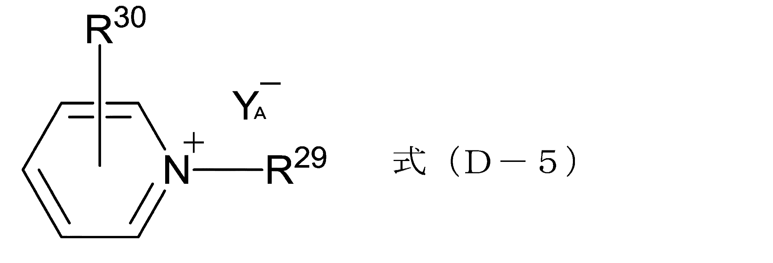
式(D-5):
式(D-6):

また、ホスホニウム塩としては、式(D-7):
また、スルホニウム塩としては、式(D-8):

Formula (D-3):
Formula (D-4):
Formula (D-5):
Formula (D-6):
Moreover, as a phosphonium salt, Formula (D-7):
Moreover, as a sulfonium salt, Formula (D-8):
半導体装置の製造に使用される基板(例えば、シリコンウエハー基板、シリコン/二酸化シリコン被覆基板、シリコンナイトライド基板、ガラス基板、ITO基板、ポリイミド基板、及び低誘電率材料(low-k材料)被覆基板等)の上に、スピナー、コーター等の適当な塗布方法により本発明のレジスト下層膜形成組成物が塗布され、その後、焼成することによりレジスト下層膜が形成される。焼成する条件としては、焼成温度80℃乃至250℃、焼成時間0.3分間乃至60分間の中から適宜、選択される。好ましくは、焼成温度150℃乃至250℃、焼成時間0.5分間乃至2分間である。ここで、形成される下層膜の膜厚としては、例えば、10nm乃至1000nmであり、又は20nm乃至500nmであり、又は50nm乃至300nmであり、又は100nm乃至200nmである。 Hereinafter, use of the resist underlayer film forming composition of the present invention will be described.
Substrates used for manufacturing semiconductor devices (for example, silicon wafer substrates, silicon / silicon dioxide coated substrates, silicon nitride substrates, glass substrates, ITO substrates, polyimide substrates, and low dielectric constant material (low-k material) coated substrates The resist underlayer film forming composition of the present invention is coated on a etc.) by a suitable coating method such as a spinner or a coater, and thereafter, a resist underlayer film is formed by baking. The firing conditions are appropriately selected from a firing temperature of 80 ° C. to 250 ° C. and a firing time of 0.3 minutes to 60 minutes. Preferably, the baking temperature is 150 ° C. to 250 ° C., and the baking time is 0.5 minutes to 2 minutes. Here, the thickness of the lower layer film to be formed is, for example, 10 nm to 1000 nm, or 20 nm to 500 nm, or 50 nm to 300 nm, or 100 nm to 200 nm.
フッ素系ガスとしては、例えば、テトラフルオロメタン(CF4)、パーフルオロシクロブタン(C4F8)、パーフルオロプロパン(C3F8)、トリフルオロメタン、及びジフルオロメタン(CH2F2)等が挙げられる。 Finally, processing of the semiconductor substrate is performed. The processing of the semiconductor substrate is preferably performed by dry etching with a fluorine-based gas.
As the fluorine-based gas, for example, tetrafluoromethane (CF 4 ), perfluorocyclobutane (C 4 F 8 ), perfluoropropane (C 3 F 8 ), trifluoromethane, difluoromethane (CH 2 F 2 ), etc. It can be mentioned.
これらのアルカリ水溶液の濃度は2.38質量%濃度で使用することも可能であるが、10質量%、20質量%、又は30質量%の高濃度のアルカリ水溶液を使用することもできる。 After processing of the substrate, the resist underlayer film used for substrate processing remaining on the substrate can be removed with an aqueous alkaline solution. For example, a tetramethyl ammonium hydroxide aqueous solution or a tetraethyl ammonium hydroxide aqueous solution can be used as this alkaline aqueous solution.
Although the concentration of these aqueous alkali solutions can be used at a concentration of 2.38% by mass, a high concentration aqueous alkali solution of 10% by mass, 20% by mass or 30% by mass can also be used.
テトラエトキシシラン20.0g、フェニルトリメトキシシラン1.5g、5-(トリエトキシシリル)ヘキサヒドロ-4,7-メタノイソベンゾフラン-1,3-ジオン14.6g、アセトン54.2gを300mlのフラスコに入れ、混合溶液をマグネチックスターラーにて撹拌しながら0.01M塩酸水溶液9.7gを混合溶液に滴下した。添加後、85℃に調整されたオイルバスにフラスコを移し、240分間、還流させた。その後、プロピレングリコールモノメチルエーテルを72g加え、アセトン、メタノール、エタノール、水を減圧留去し、濃縮して加水分解縮合物(ポリマー)水溶液を得た。さらにプロピレングリコールモノメチルエーテルを加え、140℃における固形残物換算で13質量パーセントとなるように調整した。得られたポリマーは式(4-1)に相当し、GPCによる重量平均分子量Mwはポリスチレン換算で1500であった。5-(トリエトキシシリル)ヘキサヒドロ-4,7-メタノイソベンゾフラン-1,3-ジオンは全シラン中に30モル%の割合で含まれていた。 Synthesis Example 1
20.0 g of tetraethoxysilane, 1.5 g of phenyltrimethoxysilane, 14.6 g of 5- (triethoxysilyl) hexahydro-4,7-methanoisobenzofuran-1,3-dione, 54.2 g of acetone in a 300 ml flask Then, 9.7 g of 0.01 M aqueous hydrochloric acid solution was added dropwise to the mixed solution while stirring the mixed solution with a magnetic stirrer. After the addition, the flask was transferred to an oil bath adjusted to 85 ° C. and refluxed for 240 minutes. Thereafter, 72 g of propylene glycol monomethyl ether was added, and acetone, methanol, ethanol and water were distilled off under reduced pressure and concentrated to obtain an aqueous solution of hydrolytic condensate (polymer). Furthermore, propylene glycol monomethyl ether was added, and it adjusted so that it might become 13 mass% in conversion of solid residue at 140 degreeC. The obtained polymer corresponded to Formula (4-1), and the weight average molecular weight Mw by GPC was 1,500 in terms of polystyrene. 5- (triethoxysilyl) hexahydro-4,7-methanoisobenzofuran-1,3-dione was contained in a proportion of 30 mol% in the total silane.
テトラエトキシシラン19.5g、5-(トリエトキシシリル)ヘキサヒドロ-4,7-メタノイソベンゾフラン-1,3-ジオン14.2g、N-(3-(トリエトキシシリル)プロピル)ベンゼンスルホンアミド2.6g、アセトン54.3gを300mlのフラスコに入れ、混合溶液をマグネチックスターラーにて撹拌しながら0.1M硝酸水溶液9.5gを混合溶液に滴下した。添加後、85℃に調整されたオイルバスにフラスコを移し、240分間、還流させた。その後、プロピレングリコールモノメチルエーテルを72g加え、アセトン、メタノール、エタノール、水を減圧留去し、濃縮して加水分解縮合物(ポリマー)水溶液を得た。さらにプロピレングリコールモノメチルエーテルを加え、140℃における固形残物換算で13質量パーセントとなるように調整した。得られたポリマーは式(4-2)に相当し、GPCによる重量平均分子量Mwはポリスチレン換算で1500であった。5-(トリエトキシシリル)ヘキサヒドロ-4,7-メタノイソベンゾフラン-1,3-ジオンは全シラン中に30モル%の割合で含まれていた。 (Composition example 2)
19.5 g of tetraethoxysilane, 14.2 g of 5- (triethoxysilyl) hexahydro-4,7-methanoisobenzofuran-1,3-dione, N- (3- (triethoxysilyl) propyl) benzenesulfonamide 2. 6 g and 54.3 g of acetone were placed in a 300 ml flask, and 9.5 g of a 0.1 M aqueous nitric acid solution was added dropwise to the mixed solution while stirring the mixed solution with a magnetic stirrer. After the addition, the flask was transferred to an oil bath adjusted to 85 ° C. and refluxed for 240 minutes. Thereafter, 72 g of propylene glycol monomethyl ether was added, and acetone, methanol, ethanol and water were distilled off under reduced pressure and concentrated to obtain an aqueous solution of hydrolytic condensate (polymer). Furthermore, propylene glycol monomethyl ether was added, and it adjusted so that it might become 13 mass% in conversion of solid residue at 140 degreeC. The obtained polymer corresponded to Formula (4-2), and the weight average molecular weight Mw by GPC was 1,500 in terms of polystyrene. 5- (triethoxysilyl) hexahydro-4,7-methanoisobenzofuran-1,3-dione was contained in a proportion of 30 mol% in the total silane.
テトラエトキシシラン18.2g、ジ-tert-ブチル2-(3-(トリエトキシシリル)プロピル)マロネート16.9g、フェニルトリメトキシシラン1.33g、アセトン54.7gを300mlのフラスコに入れ、混合溶液をマグネチックスターラーにて撹拌しながら0.01M塩酸水溶液8.8gを混合溶液に滴下した。添加後、85℃に調整されたオイルバスにフラスコを移し、240分間、還流させた。その後、プロピレングリコールモノメチルエーテルを72g加え、アセトン、メタノール、エタノール、水を減圧留去し、濃縮して加水分解縮合物(ポリマー)水溶液を得た。さらにプロピレングリコールモノメチルエーテルを加え、140℃における固形残物換算で13質量パーセントとなるように調整した。得られたポリマーは式(4-3)に相当し、GPCによる重量平均分子量Mwはポリスチレン換算で1500であった。ジ-tert-ブチル2-(3-(トリエトキシシリル)プロピル)マロネートは全シラン中に30モル%の割合で含まれていた。 (Composition example 3)
18.2 g of tetraethoxysilane, 16.9 g of di-tert-butyl 2- (3- (triethoxysilyl) propyl) malonate, 1.33 g of phenyltrimethoxysilane, and 54.7 g of acetone are placed in a 300 ml flask and mixed solution Was stirred with a magnetic stirrer, and 8.8 g of 0.01 M aqueous hydrochloric acid solution was added dropwise to the mixed solution. After the addition, the flask was transferred to an oil bath adjusted to 85 ° C. and refluxed for 240 minutes. Thereafter, 72 g of propylene glycol monomethyl ether was added, and acetone, methanol, ethanol and water were distilled off under reduced pressure and concentrated to obtain an aqueous solution of hydrolytic condensate (polymer). Furthermore, propylene glycol monomethyl ether was added, and it adjusted so that it might become 13 mass% in conversion of solid residue at 140 degreeC. The obtained polymer corresponded to Formula (4-3), and the weight average molecular weight Mw by GPC was 1,500 in terms of polystyrene. Di-tert-butyl 2- (3- (triethoxysilyl) propyl) malonate was contained in a proportion of 30 mol% in the total silane.
テトラエトキシシラン17.7g、ジ-tert-ブチル2-(3-(トリエトキシシリル)プロピル)マロネート16.5g、N-(3-(トリエトキシシリル)プロピル)ベンゼンスルホンアミド2.4g、アセトン54.8gを300mlのフラスコに入れ、混合溶液をマグネチックスターラーにて撹拌しながら0.01M塩酸水溶液8.8gを混合溶液に滴下した。添加後、85℃に調整されたオイルバスにフラスコを移し、240分間、還流させた。その後、プロピレングリコールモノメチルエーテルを72g加え、アセトン、メタノール、エタノール、水を減圧留去し、濃縮して加水分解縮合物(ポリマー)水溶液を得た。さらにプロピレングリコールモノメチルエーテルを加え、140℃における固形残物換算で13質量パーセントとなるように調整した。得られたポリマーは式(4-4)に相当し、GPCによる重量平均分子量Mwはポリスチレン換算で1500であった。ジ-tert-ブチル2-(3-(トリエトキシシリル)プロピル)マロネートは全シラン中に30モル%の割合で含まれていた。 (Composition example 4)
17.7 g of tetraethoxysilane, 16.5 g of di-tert-butyl 2- (3- (triethoxysilyl) propyl) malonate, 2.4 g of N- (3- (triethoxysilyl) propyl) benzenesulfonamide, acetone 54 8 g was put into a 300 ml flask, and while stirring the mixed solution with a magnetic stirrer, 8.8 g of 0.01 M aqueous hydrochloric acid solution was dropped to the mixed solution. After the addition, the flask was transferred to an oil bath adjusted to 85 ° C. and refluxed for 240 minutes. Thereafter, 72 g of propylene glycol monomethyl ether was added, and acetone, methanol, ethanol and water were distilled off under reduced pressure and concentrated to obtain an aqueous solution of hydrolytic condensate (polymer). Furthermore, propylene glycol monomethyl ether was added, and it adjusted so that it might become 13 mass% in conversion of solid residue at 140 degreeC. The obtained polymer corresponded to Formula (4-4), and the weight average molecular weight Mw by GPC was 1,500 in terms of polystyrene. Di-tert-butyl 2- (3- (triethoxysilyl) propyl) malonate was contained in a proportion of 30 mol% in the total silane.
テトラエトキシシラン20.6g、3-(3-(トリエトキシシリル)プロピル)ジヒドロフラン-2,5-ジオン13.9g、フェニルトリメトキシシラン1.51g、アセトン54.0gを300mlのフラスコに入れ、混合溶液をマグネチックスターラーにて撹拌しながら0.01M塩酸水溶液10.0gを混合溶液に滴下した。添加後、85℃に調整されたオイルバスにフラスコを移し、240分間、還流させた。その後、プロピレングリコールモノメチルエーテルを72g加え、アセトン、メタノール、エタノール、水を減圧留去し、濃縮して加水分解縮合物(ポリマー)水溶液を得た。さらにプロピレングリコールモノメチルエーテルを加え、140℃における固形残物換算で13質量パーセントとなるように調整した。得られたポリマーは式(4-5)に相当し、GPCによる重量平均分子量Mwはポリスチレン換算で1500であった。3-(3-(トリエトキシシリル)プロピル)ジヒドロフラン-2,5-ジオンは全シラン中に30モル%の割合で含まれていた。 (Composition example 5)
20.6 g of tetraethoxysilane, 13.9 g of 3- (3- (triethoxysilyl) propyl) dihydrofuran-2,5-dione, 1.51 g of phenyltrimethoxysilane, and 54.0 g of acetone are placed in a 300 ml flask, While stirring the mixed solution with a magnetic stirrer, 10.0 g of 0.01 M aqueous hydrochloric acid solution was added dropwise to the mixed solution. After the addition, the flask was transferred to an oil bath adjusted to 85 ° C. and refluxed for 240 minutes. Thereafter, 72 g of propylene glycol monomethyl ether was added, and acetone, methanol, ethanol and water were distilled off under reduced pressure and concentrated to obtain an aqueous solution of hydrolytic condensate (polymer). Furthermore, propylene glycol monomethyl ether was added, and it adjusted so that it might become 13 mass% in conversion of solid residue at 140 degreeC. The obtained polymer corresponded to Formula (4-5), and the weight average molecular weight Mw by GPC was 1,500 in terms of polystyrene. 3- (3- (triethoxysilyl) propyl) dihydrofuran-2,5-dione was contained in a proportion of 30 mol% in the total silane.
テトラエトキシシラン20.0g、3-(3-(トリエトキシシリル)プロピル)ジヒドロフラン-2,5-ジオン13.5g、N-(3-(トリエトキシシリル)プロピル)ベンゼンスルホンアミド2.67g、アセトン54.2gを300mlのフラスコに入れ、混合溶液をマグネチックスターラーにて撹拌しながら0.01M塩酸水溶液9.7gを混合溶液に滴下した。添加後、85℃に調整されたオイルバスにフラスコを移し、240分間、還流させた。その後、プロピレングリコールモノメチルエーテルを72g加え、アセトン、メタノール、エタノール、水を減圧留去し、濃縮して加水分解縮合物(ポリマー)水溶液を得た。さらにプロピレングリコールモノメチルエーテルを加え、140℃における固形残物換算で13質量パーセントとなるように調整した。得られたポリマーは式(4-6)に相当し、GPCによる重量平均分子量Mwはポリスチレン換算で1500であった。3-(3-(トリエトキシシリル)プロピル)ジヒドロフラン-2,5-ジオンは全シラン中に30モル%の割合で含まれていた。 Synthesis Example 6
20.0 g of tetraethoxysilane, 13.5 g of 3- (3- (triethoxysilyl) propyl) dihydrofuran-2,5-dione, 2.67 g of N- (3- (triethoxysilyl) propyl) benzenesulfonamide, 54.2 g of acetone was placed in a 300 ml flask, and 9.7 g of 0.01 M aqueous hydrochloric acid solution was added dropwise to the mixed solution while stirring the mixed solution with a magnetic stirrer. After the addition, the flask was transferred to an oil bath adjusted to 85 ° C. and refluxed for 240 minutes. Thereafter, 72 g of propylene glycol monomethyl ether was added, and acetone, methanol, ethanol and water were distilled off under reduced pressure and concentrated to obtain an aqueous solution of hydrolytic condensate (polymer). Furthermore, propylene glycol monomethyl ether was added, and it adjusted so that it might become 13 mass% in conversion of solid residue at 140 degreeC. The obtained polymer corresponded to Formula (4-6), and the weight average molecular weight Mw by GPC was 1,500 in terms of polystyrene. 3- (3- (triethoxysilyl) propyl) dihydrofuran-2,5-dione was contained in a proportion of 30 mol% in the total silane.
テトラエトキシシラン12.8g、5-(トリエトキシシリル)ヘキサヒドロ-4,7-メタノイソベンゾフラン-1,3-ジオン22.4g、フェニルトリメトキシシラン1.35g、アセトン54.9gを300mlのフラスコに入れ、混合溶液をマグネチックスターラーにて撹拌しながら0.01M塩酸水溶液8.5gを混合溶液に滴下した。添加後、85℃に調整されたオイルバスにフラスコを移し、240分間、還流させた。その後、プロピレングリコールモノメチルエーテルを72g加え、アセトン、メタノール、エタノール、水を減圧留去し、濃縮して加水分解縮合物(ポリマー)水溶液を得た。さらにプロピレングリコールモノメチルエーテルを加え、140℃における固形残物換算で13質量パーセントとなるように調整した。得られたポリマーは式(4-7)に相当し、GPCによる重量平均分子量Mwはポリスチレン換算で1500であった。5-(トリエトキシシリル)ヘキサヒドロ-4,7-メタノイソベンゾフラン-1,3-ジオンは全シラン中に50モル%の割合で含まれていた。 Synthesis Example 7
12.8 g of tetraethoxysilane, 22.4 g of 5- (triethoxysilyl) hexahydro-4,7-methanoisobenzofuran-1,3-dione, 1.35 g of phenyltrimethoxysilane, 54.9 g of acetone in a 300 ml flask Then, 8.5 g of 0.01 M aqueous hydrochloric acid solution was added dropwise to the mixed solution while stirring the mixed solution with a magnetic stirrer. After the addition, the flask was transferred to an oil bath adjusted to 85 ° C. and refluxed for 240 minutes. Thereafter, 72 g of propylene glycol monomethyl ether was added, and acetone, methanol, ethanol and water were distilled off under reduced pressure and concentrated to obtain an aqueous solution of hydrolytic condensate (polymer). Furthermore, propylene glycol monomethyl ether was added, and it adjusted so that it might become 13 mass% in conversion of solid residue at 140 degreeC. The obtained polymer corresponded to Formula (4-7), and the weight average molecular weight Mw by GPC was 1,500 in terms of polystyrene. 5- (triethoxysilyl) hexahydro-4,7-methanoisobenzofuran-1,3-dione was contained in a proportion of 50 mol% in the total silane.
テトラエトキシシラン17.2g、5-(トリエトキシシリル)ヘキサヒドロ-4,7-メタノイソベンゾフラン-1,3-ジオン13.5g、トリエトキシシリルプロピルジアリルイソシアヌレート5.69g、アセトン54.6gを300mlのフラスコに入れ、混合溶液をマグネチックスターラーにて撹拌しながら0.01M塩酸水溶液8.9gを混合溶液に滴下した。添加後、85℃に調整されたオイルバスにフラスコを移し、240分間、還流させた。その後、プロピレングリコールモノメチルエーテルを72g加え、アセトン、メタノール、エタノール、水を減圧留去し、濃縮して加水分解縮合物(ポリマー)水溶液を得た。さらにプロピレングリコールモノメチルエーテルを加え、140℃における固形残物換算で13質量パーセントとなるように調整した。得られたポリマーは式(4-8)に相当し、GPCによる重量平均分子量Mwはポリスチレン換算で1500であった。5-(トリエトキシシリル)ヘキサヒドロ-4,7-メタノイソベンゾフラン-1,3-ジオンは全シラン中に30モル%の割合で含まれていた。 Synthesis Example 8
17.2 g of tetraethoxysilane, 13.5 g of 5- (triethoxysilyl) hexahydro-4,7-methanoisobenzofuran-1,3-dione, 5.69 g of triethoxysilylpropyldiallylisocyanurate, 300 ml of 54.6 g of acetone The mixture was placed in a flask, and 8.9 g of 0.01 M aqueous hydrochloric acid solution was added dropwise to the mixed solution while stirring the mixed solution with a magnetic stirrer. After the addition, the flask was transferred to an oil bath adjusted to 85 ° C. and refluxed for 240 minutes. Thereafter, 72 g of propylene glycol monomethyl ether was added, and acetone, methanol, ethanol and water were distilled off under reduced pressure and concentrated to obtain an aqueous solution of hydrolytic condensate (polymer). Furthermore, propylene glycol monomethyl ether was added, and it adjusted so that it might become 13 mass% in conversion of solid residue at 140 degreeC. The obtained polymer corresponded to Formula (4-8), and the weight average molecular weight Mw by GPC was 1,500 in terms of polystyrene. 5- (triethoxysilyl) hexahydro-4,7-methanoisobenzofuran-1,3-dione was contained in a proportion of 30 mol% in the total silane.
35wt%テトラエチルアンモニウムヒドロキシド水溶液0.81g、水1.30g、イソプロピルアルコール27.63g、メチルイソブチルケトン55.25gを300mlのフラスコに入れ、混合溶液をマグネチックスターラーにて撹拌しながら(4-(1-エトキシエトキシ)フェニル)トリメトキシシラン27.6gを混合溶液に滴下した。添加後、40℃に調整されたオイルバスにフラスコを移し、240分間、反応させた。その後、反応溶液に1M硝酸48.2gを加え、さらに40℃にてエトキシエトキシ基を脱保護しフェノール基を有する加水分解縮合物を得た。その後、メチルイソブチルケトン165.76g、水82.88gを加え、分液操作にて水層に移行した反応副生物である水、硝酸、テトラエチルアンモニウム硝酸塩を留去し、有機層を回収した。その後、プロピレングリコールモノメチルエーテルを82.88g加え、メチルイソブチルケトン、メタノール、エタノール、水を減圧留去し、濃縮して加水分解縮合物(ポリマー)水溶液を得た。さらにプロピレングリコールモノメチルエーテルを加え、プロピレングリコールモノメチルエーテル100%の溶媒比率として140℃における固形残物換算で20質量パーセントとなるように調整した。得られたポリマーは式(4-9)に相当し、GPCによる重量平均分子量Mwはポリスチレン換算で2500であった。(4-(1-エトキシエトキシ)フェニル)トリメトキシシランのエトキシエトキシ基を脱保護したフェノール基含有ユニットが全シラン中に100モル%の割合で含まれていた。 Synthesis Example 9
A 300 ml flask is charged with 0.81 g of a 35 wt% aqueous solution of tetraethylammonium hydroxide, 1.30 g of water, 27.63 g of isopropyl alcohol and 55.25 g of methyl isobutyl ketone, and the mixed solution is stirred with a magnetic stirrer (4- 27.6 g of 1-ethoxyethoxy) phenyl) trimethoxysilane was dropped into the mixed solution. After the addition, the flask was transferred to an oil bath adjusted to 40 ° C. and allowed to react for 240 minutes. Thereafter, 48.2 g of 1 M nitric acid was added to the reaction solution, and the ethoxyethoxy group was further deprotected at 40 ° C. to obtain a hydrolysis condensation product having a phenol group. Thereafter, 165.76 g of methyl isobutyl ketone and 82.88 g of water were added, and water, nitric acid, and tetraethylammonium nitrate, which are reaction by-products transferred to the aqueous layer by liquid separation operation, were distilled off, and the organic layer was recovered. Thereafter, 82.88 g of propylene glycol monomethyl ether was added, and methyl isobutyl ketone, methanol, ethanol and water were distilled off under reduced pressure and concentrated to obtain an aqueous solution of hydrolytic condensate (polymer). Furthermore, propylene glycol monomethyl ether was added, and it adjusted so that it might become 20 mass% in conversion of solid residue in 140 degreeC as a solvent ratio of 100% of propylene glycol monomethyl ether. The obtained polymer corresponded to Formula (4-9), and the weight average molecular weight Mw by GPC was 2,500 in terms of polystyrene. A phenol group-containing unit in which the ethoxyethoxy group of (4- (1-ethoxyethoxy) phenyl) trimethoxysilane was deprotected was contained in a proportion of 100 mol% in the total silane.
35wt%テトラエチルアンモニウムヒドロキシド水溶液0.78g、水1.24g、イソプロピルアルコール27.34g、メチルイソブチルケトン54.67gを300mlのフラスコに入れ、混合溶液をマグネチックスターラーにて撹拌しながら5-(トリエトキシシリル)ヘキサヒドロ-4,7-メタノイソベンゾフラン-1,3-ジオン27.34g、(4-(1-エトキシエトキシ)フェニル)トリメトキシシラン2.65gを混合溶液に滴下した。添加後、40℃に調整されたオイルバスにフラスコを移し、240分間、反応させた。その後、反応溶液に1M硝酸46.2gを加え、さらに40℃にてエトキシエトキシ基を脱保護したフェノール基とジカルボン酸基を有する加水分解縮合物を得た。その後、メチルイソブチルケトン164.0g、水82.0gを加え、分液操作にて水層に移行した反応副生物である水、硝酸、テトラエチルアンモニウム硝酸塩を留去し、有機層を回収した。その後、プロピレングリコールモノメチルエーテルを82.0g加え、メチルイソブチルケトン、メタノール、エタノール、水を減圧留去し、濃縮して加水分解縮合物(ポリマー)水溶液を得た。さらにプロピレングリコールモノメチルエーテルを加え、プロピレングリコールモノメチルエーテル100%の溶媒比率として140℃における固形残物換算で20質量パーセントとなるように調整した。得られたポリマーは式(4-10)に相当し、GPCによる重量平均分子量Mwはポリスチレン換算で2000であった。(4-(1-エトキシエトキシ)フェニル)トリメトキシシランのエトキシエトキシ基を脱保護したフェノール基含有ユニットが全シラン中に10モル%の割合で含まれ、5-(トリエトキシシリル)ヘキサヒドロ-4,7-メタノイソベンゾフラン-1,3-ジオンを加水分解して得られたジカルボン酸含有ユニットが全シラン中に90モル%の割合で含まれていた。 Synthesis Example 10
A 300 ml flask is charged with 0.78 g of a 35 wt% aqueous solution of tetraethylammonium hydroxide, 1.24 g of water, 27.34 g of isopropyl alcohol and 54.67 g of methyl isobutyl ketone, and the mixed solution is stirred with a magnetic stirrer to give 5- (tri) 27.34 g of ethoxysilyl) hexahydro-4,7-methanoisobenzofuran-1,3-dione and 2.65 g of (4- (1-ethoxyethoxy) phenyl) trimethoxysilane were added dropwise to the mixed solution. After the addition, the flask was transferred to an oil bath adjusted to 40 ° C. and allowed to react for 240 minutes. Thereafter, 46.2 g of 1 M nitric acid was added to the reaction solution, and the ethoxyethoxy group was further deprotected at 40 ° C. to obtain a hydrolytic condensate having a phenol group and a dicarboxylic acid group. Thereafter, 164.0 g of methyl isobutyl ketone and 82.0 g of water were added, and water, nitric acid, and tetraethylammonium nitrate, which are reaction by-products transferred to the aqueous layer by liquid separation operation, were distilled off, and the organic layer was recovered. Thereafter, 82.0 g of propylene glycol monomethyl ether was added, and methyl isobutyl ketone, methanol, ethanol and water were distilled off under reduced pressure and concentrated to obtain an aqueous solution of hydrolytic condensate (polymer). Furthermore, propylene glycol monomethyl ether was added, and it adjusted so that it might become 20 mass% in conversion of solid residue in 140 degreeC as a solvent ratio of 100% of propylene glycol monomethyl ether. The obtained polymer corresponded to Formula (4-10), and the weight average molecular weight Mw by GPC was 2,000 in terms of polystyrene. A phenol group-containing unit obtained by deprotecting the ethoxyethoxy group of (4- (1-ethoxyethoxy) phenyl) trimethoxysilane is contained in a proportion of 10 mol% in the total silane, 5- (triethoxysilyl) hexahydro-4 The dicarboxylic acid-containing unit obtained by hydrolyzing 7,7-methanoisobenzofuran-1,3-dione was contained in a proportion of 90 mol% in the total silane.
35wt%テトラエチルアンモニウムヒドロキシド水溶液0.86g、水1.38g、イソプロピルアルコール28.15g、メチルイソブチルケトン56.30gを300mlのフラスコに入れ、混合溶液をマグネチックスターラーにて撹拌しながら3-(3-(トリエトキシシリル)プロピル)ジヒドロフラン-2,5-ジオン28.15g、(4-(1-エトキシエトキシ)フェニル)トリメトキシシラン2.94gを混合溶液に滴下した。添加後、40℃に調整されたオイルバスにフラスコを移し、240分間、反応させた。その後、反応溶液に1M硝酸51.4gを加え、さらに40℃にてエトキシエトキシ基を脱保護したフェノール基とジカルボン酸基を有する加水分解縮合物を得た。その後、メチルイソブチルケトン168.9g、水84.5gを加え、分液操作にて水層に移行した反応副生物である水、硝酸、テトラエチルアンモニウム硝酸塩を留去し、有機層を回収した。その後、プロピレングリコールモノメチルエーテルを84.5g加え、メチルイソブチルケトン、メタノール、エタノール、水を減圧留去し、濃縮して加水分解縮合物(ポリマー)水溶液を得た。さらにプロピレングリコールモノメチルエーテルを加え、プロピレングリコールモノメチルエーテル100%の溶媒比率として140℃における固形残物換算で20質量パーセントとなるように調整した。得られたポリマーは式(4-11)に相当し、GPCによる重量平均分子量Mwはポリスチレン換算で2100であった。(4-(1-エトキシエトキシ)フェニル)トリメトキシシランのエトキシエトキシ基を脱保護したフェノール基含有ユニットが全シラン中に10モル%の割合で含まれ、3-(3-(トリエトキシシリル)プロピル)ジヒドロフラン-2,5-ジオンを加水分解して得られたジカルボン酸含有ユニットが全シラン中に90モル%の割合で含まれていた。 Synthesis Example 11
A 300 ml flask was charged with 0.86 g of 35 wt% aqueous solution of tetraethylammonium hydroxide, 1.38 g of water, 28.15 g of isopropyl alcohol and 56.30 g of methyl isobutyl ketone, and the mixed solution was stirred with a magnetic stirrer 3- (3 28.15 g of-(triethoxysilyl) propyl) dihydrofuran-2,5-dione and 2.94 g of (4- (1-ethoxyethoxy) phenyl) trimethoxysilane were added dropwise to the mixed solution. After the addition, the flask was transferred to an oil bath adjusted to 40 ° C. and allowed to react for 240 minutes. Thereafter, 51.4 g of 1 M nitric acid was added to the reaction solution, and the ethoxyethoxy group was further deprotected at 40 ° C. to obtain a hydrolytic condensate having a phenol group and a dicarboxylic acid group. Thereafter, 168.9 g of methyl isobutyl ketone and 84.5 g of water were added, and water, nitric acid, and tetraethylammonium nitrate which are reaction by-products transferred to the aqueous layer by liquid separation operation were distilled off, and the organic layer was recovered. Thereafter, 84.5 g of propylene glycol monomethyl ether was added, and methyl isobutyl ketone, methanol, ethanol and water were distilled off under reduced pressure and concentrated to obtain an aqueous solution of hydrolytic condensate (polymer). Furthermore, propylene glycol monomethyl ether was added, and it adjusted so that it might become 20 mass% in conversion of solid residue in 140 degreeC as a solvent ratio of 100% of propylene glycol monomethyl ether. The obtained polymer corresponded to Formula (4-11), and the weight average molecular weight Mw by GPC was 2100 in terms of polystyrene. A phenol-containing unit in which the ethoxyethoxy group of (4- (1-ethoxyethoxy) phenyl) trimethoxysilane is deprotected is contained in a proportion of 10 mol% in the total silane, 3- (3- (triethoxysilyl) A dicarboxylic acid-containing unit obtained by hydrolyzing propyl) dihydrofuran-2,5-dione was contained in a proportion of 90 mol% in the total silane.
テトラエトキシシラン24.1g、フェニルトリメトキシシラン1.8g、トリエトキシメチルシラン9.5g、アセトン53.0gを300mlのフラスコに入れ、混合溶液をマグネチックスターラーにて撹拌しながら0.01M塩酸水溶液11.7gを混合溶液に滴下した。添加後、85℃に調整されたオイルバスにフラスコを移し、240分間、還流させた。その後、プロピレングリコールモノメチルエーテルを70g加え、アセトン、メタノール、エタノール、水を減圧留去し、濃縮して加水分解縮合物(ポリマー)水溶液を得た。さらにプロピレングリコールモノメチルエーテルを加え、140℃における固形残物換算で13質量パーセントとなるように調整した。得られたポリマーは式(5-1)に相当し、GPCによる重量平均分子量Mwはポリスチレン換算で1400であった。

A 300 ml flask is charged with 24.1 g of tetraethoxysilane, 1.8 g of phenyltrimethoxysilane, 9.5 g of triethoxymethylsilane, and 53.0 g of acetone, and the mixed solution is stirred with a magnetic stirrer with an aqueous 0.01 M hydrochloric acid solution. 11.7 g was dropped to the mixed solution. After the addition, the flask was transferred to an oil bath adjusted to 85 ° C. and refluxed for 240 minutes. Thereafter, 70 g of propylene glycol monomethyl ether was added, and acetone, methanol, ethanol and water were distilled off under reduced pressure and concentrated to obtain an aqueous solution of hydrolytic condensate (polymer). Furthermore, propylene glycol monomethyl ether was added, and it adjusted so that it might become 13 mass% in conversion of solid residue at 140 degreeC. The obtained polymer corresponded to Formula (5-1), and the weight average molecular weight Mw by GPC was 1400 in terms of polystyrene.
上記合成例1で得られたケイ素含有ポリマー、酸、溶媒を表1及び表2に示す割合で混合し、0.1μmのフッ素樹脂製のフィルターで濾過することによって、ポリマー含有塗布液をそれぞれ調製した。表1及び表2中のポリマーの添加割合はポリマー溶液の添加量ではなく、ポリマー自体の添加量を示した。
TPSMale(光酸発生剤)はトリフェニルスルホニウムマレイン酸を示し、TPSNO3(光酸発生剤)はトリフェニルスルホニウム硝酸塩を示し、TPSCS(光酸発生剤)はトリフェニルスルホニウムカンファスルホン酸塩を示し、TPSTFA(光酸発生剤)はトリフェニルスルホニウムトリフルオロ酢酸塩を示し、TPSNf(光酸発生剤)はトリフェニルスルホニウムノナフルオロブタンスルホネート、TPSTf(光酸発生剤)はトリフェニルスルホニウムトリフルオロメタンスルホナート、を示し、TPSAdTf(光酸発生剤)はトリフェニルスルホニウムアダマンタンカルボン酸ブチルトリフルオロメタンスルホン酸を示し、ImideTEOSは4,5-ジヒドロイミダゾールプロピルトリエトキシシランを示し、TPSCl(光酸発生剤)はトリフェニルスルホニウムクロライドを示し、TPSAc(光酸発生剤)はトリフェニルスルホニウム酢酸塩を示し、TPSMS(光酸発生剤)はトリフルオロメタンスルホニウムメタンスルホネートを示し、Tris-VEはトリス(4-(ビニリロキシ)ブチル)ベンゼン-1,3,5-トリカルボキシレートを示し、PGMEはプロピレングリコールモノメチルエーテルを示し、PGMEAはプロピレングリコールモノメチルエーテルアセテートを示す。各添加量は質量部で示した。 (Preparation of Si-containing resist underlayer film)
The polymer containing coating liquid is prepared by mixing the silicon-containing polymer, the acid, and the solvent obtained in the above Synthesis Example 1 in the proportions shown in Tables 1 and 2 and filtering with a 0.1 μm fluororesin filter. did. The addition ratio of the polymer in Tables 1 and 2 indicates the addition amount of the polymer itself, not the addition amount of the polymer solution.
TPSMale (photoacid generator) indicates triphenylsulfonium maleic acid, TPSNO3 (photoacid generator) indicates triphenylsulfonium nitrate, TPSCS (photoacid generator) indicates triphenylsulfonium camphorsulfonate, TPSTFA (Photoacid generator) indicates triphenylsulfonium trifluoroacetate, TPSNf (photoacid generator) is triphenylsulfonium nonafluorobutanesulfonate, and TPSTf (photoacid generator) is triphenylsulfonium trifluoromethanesulfonate, TPSAdTf (photoacid generator) represents triphenylsulfonium adamantanecarboxylic acid butyl trifluoromethanesulfonic acid; ImideTEOS represents 4,5-dihydroimidazolepropyltriethoxysilane; PSCl (photoacid generator) indicates triphenylsulfonium chloride, TPSAc (photoacid generator) indicates triphenylsulfonium acetate, TPSMS (photoacid generator) indicates trifluoromethanesulfonium methanesulfonate, Tris-VE Represents tris (4- (vinylyloxy) butyl) benzene-1,3,5-tricarboxylate, PGME represents propylene glycol monomethyl ether, and PGMEA represents propylene glycol monomethyl ether acetate. Each addition amount was shown by the mass part.


窒素下、100mL四口フラスコにカルバゾール(6.69g、0.040mol、東京化成工業(株)製)、9-フルオレノン(7.28g、0.040mol、東京化成工業(株)製)、パラトルエンスルホン酸一水和物(0.76g、0.0040mol、東京化成工業(株)製)を加え、1,4-ジオキサン(6.69g、関東化学(株)製)を仕込み撹拌し、100℃まで昇温し溶解させ重合を開始した。24時間後60℃まで放冷後、クロロホルム(34g、関東化学(株)製)を加え希釈し、メタノール(168g、関東化学(株)製)へ再沈殿させた。得られた沈殿物をろ過し、減圧乾燥機で80℃、24時間乾燥し、目的とするポリマー(式(6-1)、以下PCzFLと略す)9.37gを得た。

1H-NMR(400MHz,DMSO-d6):δ7.03-7.55(br,12H),δ7.61-8.10(br,4H),δ11.18(br,1H)
PCzFLのGPCによるポリスチレン換算で測定される重量平均分子量Mwは2800、多分散度Mw/Mnは1.77であった。
得られた樹脂20gに、架橋剤としてテトラメトキシメチルグリコールウリル(三井サイテック(株)製、商品名パウダーリンク1174)3.0g、触媒としてピリジニウムパラトルエンスルホネート0.30g、界面活性剤としてメガファックR-30(DIC(株)製、商品名)0.06gを混合し、プロピレングリコールモノメチルエーテルアセテート88gに溶解させ溶液とした。その後、孔径0.10μmのポリエチレン製ミクロフィルターを用いて濾過し、更に、孔径0.05μmのポリエチレン製ミクロフィルターを用いて濾過して、多層膜によるリソグラフィープロセスに用いる有機下層膜形成組成物の溶液を調製した。 (Preparation of organic lower layer film)
Carbazole (6.69 g, 0.040 mol, made by Tokyo Chemical Industry Co., Ltd.), 9-fluorenone (7.28 g, 0.040 mol, made by Tokyo Chemical Industry Co., Ltd.), para-toluene in a 100 mL four-necked flask under nitrogen Sulfonic acid monohydrate (0.76 g, 0.0040 mol, manufactured by Tokyo Chemical Industry Co., Ltd.) is added, 1,4-dioxane (6.69 g, manufactured by Kanto Chemical Co., Ltd.) is added, stirred, and heated to 100 ° C. The temperature was raised to dissolution and polymerization was initiated. After cooling for 24 hours to 60 ° C., chloroform (34 g, manufactured by Kanto Chemical Co., Ltd.) was added to dilute, and reprecipitated into methanol (168 g, manufactured by Kanto Chemical Co., Ltd.). The resulting precipitate was filtered and dried at 80 ° C. for 24 hours in a vacuum dryer to obtain 9.37 g of a target polymer (Formula (6-1), hereinafter abbreviated as PCzFL).
1 H-NMR (400 MHz, DMSO-d 6 ): δ 7.03-5.55 (br, 12 H), δ 7.61-8. 10 (br, 4 H), δ 11.18 (br, 1 H)
The weight average molecular weight Mw measured by polystyrene conversion by GPC of PCzFL was 2800, and the polydispersity Mw / Mn was 1.77.
To 20 g of the obtained resin, 3.0 g of tetramethoxymethyl glycoluril (Mitsui Cytec Co., Ltd., trade name: Powder Link 1174) as a crosslinking agent, 0.30 g of pyridinium paratoluene sulfonate as a catalyst, and MegaFac R as a surfactant 0.06 g of -30 (trade name, manufactured by DIC Corporation) was mixed and dissolved in 88 g of propylene glycol monomethyl ether acetate to prepare a solution. Thereafter, the solution is filtered using a polyethylene microfilter with a pore diameter of 0.10 μm, and further filtered using a polyethylene microfilter with a pore diameter of 0.05 μm, and a solution of the composition for forming an organic lower layer film used in the lithography process by multilayer film. Was prepared.
実施例1乃至実施例11、比較例1で調製したSi含有塗布液をスピナーを用い、シリコンウェハー上にそれぞれ塗布した。ホットプレート上で180℃1分間加熱し、Si含有レジスト下層膜をそれぞれ形成した。その後、プロピレングリコールモノメチルエーテル/プロピレングリコールモノメチルエーテルアセテート=7/3の溶剤をSi含有レジスト下層膜上に塗布、スピン乾燥し、溶剤塗布前後での膜厚の変化の有無を評価した。膜厚変化が1%以下のものを「良好」、膜厚変化が1%以上のものを「硬化せず」とした。
また同様にして実施例1乃至実施例11、比較例1で調製したSi含有塗布液をスピナーを用い、シリコンウェハー上にそれぞれ塗布した。ホットプレート上で180℃1分間加熱し、Si含有レジスト下層膜をそれぞれ形成した。その後、アルカリ現像液(水酸化テトラメチルアンモニウム(TMAH)2.38%水溶液)をSi含有レジスト下層膜上に塗布、スピン乾燥し、溶剤塗布前後での膜厚の変化の有無を評価した。膜厚変化が90%以上のものを「良好」、膜厚変化が90%以下のものを「溶解せず」とした。
さらに、同様にして実施例1乃至実施例11、比較例1で調製したSi含有塗布液をスピナーを用い、シリコンウェハー上にそれぞれ塗布した。ホットプレート上で180℃1分間加熱し、Si含有レジスト下層膜をそれぞれ形成した。その後、(株)ニコン製NSR-S307Eスキャナー(波長193nm、NA、σ:0.85)を用い、マスクを通さずSiウェハ全面にArF露光を行った。その後、アルカリ現像液(TMAH2.38%水溶液)をSi含有レジスト下層膜上に塗布、スピン乾燥し、溶剤塗布前後での膜厚の変化の有無を評価した。膜厚変化が90%以上のものを「良好」、膜厚変化が90%以下のものを「溶解せず」とした。また、「――」は評価を行わなかった。 (Solvent resistance, developer solubility test)
The Si-containing coating solutions prepared in Examples 1 to 11 and Comparative Example 1 were each coated on a silicon wafer using a spinner. The substrate was heated on a hot plate at 180 ° C. for 1 minute to form a Si-containing resist underlayer film. Thereafter, a solvent of propylene glycol monomethyl ether / propylene glycol monomethyl ether acetate = 7/3 was applied onto the Si-containing resist underlayer film, spin-dried, and the presence or absence of a change in film thickness before and after the solvent application was evaluated. A film thickness change of 1% or less was "good", and a film thickness change of 1% or more was "not cured".
Similarly, the Si-containing coating solutions prepared in Examples 1 to 11 and Comparative Example 1 were coated on silicon wafers using a spinner. The substrate was heated on a hot plate at 180 ° C. for 1 minute to form a Si-containing resist underlayer film. Thereafter, an alkaline developer (a 2.38% aqueous solution of tetramethylammonium hydroxide (TMAH)) was applied onto the Si-containing resist underlayer film, spin-dried, and the presence or absence of a change in film thickness before and after solvent application was evaluated. A film thickness change of 90% or more was regarded as “good”, and a film thickness change of 90% or less was regarded as “not dissolved”.
Furthermore, the Si-containing coating solutions prepared in Examples 1 to 11 and Comparative Example 1 in the same manner were coated on a silicon wafer using a spinner. The substrate was heated on a hot plate at 180 ° C. for 1 minute to form a Si-containing resist underlayer film. Thereafter, ArF exposure was performed on the entire surface of the Si wafer without passing through a mask, using NSR-S307E scanner (wavelength 193 nm, NA, σ: 0.85) manufactured by Nikon Corporation. Thereafter, an alkaline developer (TMAH 2.38% aqueous solution) was applied onto the Si-containing resist underlayer film, spin-dried, and the presence or absence of a change in film thickness before and after the solvent application was evaluated. A film thickness change of 90% or more was regarded as “good”, and a film thickness change of 90% or less was regarded as “not dissolved”. Also, "-" did not evaluate.

(レジストパターニング評価:アルカリ現像を行うPTD工程を経由した評価)
上記式(6-1)で得られた有機下層膜(A層)形成組成物をシリコンウエハー上に塗布し、ホットプレート上で240℃で60秒間ベークし、膜厚200nmの有機下層膜(A層)を得た。その上にそれぞれ、実施例2、4、6、8、10、11、比較例1で得られたSi含有レジスト下層膜(B層)形成組成物を塗布し、ホットプレート上で180℃で60秒間ベークし、Si含有レジスト下層膜(B層)を得た。Si含有レジスト下層膜(B層)の膜厚は40nmであった。
B層の上に市販のArF用レジスト溶液(JSR(株)製、商品名:AR2772JN)をスピナーによりそれぞれ塗布し、ホットプレート上で110℃にて1分間加熱し、膜厚120nmのフォトレジスト膜(C層)を形成した。
(株)ニコン製NSR-S307Eスキャナー(波長193nm、NA、σ:0.85、0.93/0.85)を用い、現像後にフォトレジストのライン幅及びそのライン間の幅が0.062μm、すなわち0.062μmのラインアンドスペース(L/S)=1/1のデンスラインが形成されるように設定されたマスクにそれぞれを通して露光を行った。その後、ホットプレート上100℃で60秒間ベークし、冷却後、2.38%アルカリ水溶液を用いて60秒現像し、レジスト下層膜(B層)上にポジ型のパターンを形成した。得られたフォトレジストパターンについて、大きなパターン剥がれやアンダーカット、ライン底部の太り(フッティング)が発生しないものを良好として評価した。また、「――」は評価を行わなかった。 [Resist pattern evaluation by ArF exposure]
(Resist patterning evaluation: Evaluation via PTD process for alkaline development)
The composition for forming an organic lower layer film (A layer) obtained by the above formula (6-1) is applied onto a silicon wafer, baked on a hot plate at 240 ° C. for 60 seconds, and an organic lower layer film (A Layer). The composition for forming the Si-containing resist underlayer film (B layer) obtained in Example 2, 4, 6, 8, 10, 11 and Comparative Example 1 is applied thereon, and the composition is heated to 60 ° C. at 180 ° C. on a hot plate. The second baking was performed to obtain a Si-containing resist underlayer film (B layer). The film thickness of the Si-containing resist underlayer film (B layer) was 40 nm.
A commercially available resist solution for ArF (manufactured by JSR Corporation, trade name: AR2772JN) is applied onto the layer B by a spinner, and heated on a hot plate at 110 ° C. for 1 minute to form a photoresist film having a thickness of 120 nm. (C layer) was formed.
Using a Nikon NSR-S307E scanner (wavelength 193 nm, NA, σ: 0.85, 0.93 / 0.85), after development, the photoresist line width and the line width between the lines are 0.062 μm, That is, exposure was performed through each of the masks set such that a line and space (L / S) = 1/1 density line of 0.062 μm was formed. Thereafter, the resultant was baked at 100 ° C. for 60 seconds on a hot plate, cooled, and developed for 60 seconds using a 2.38% alkaline aqueous solution to form a positive pattern on the resist underlayer film (B layer). The obtained photoresist patterns were evaluated as good if large pattern peeling, undercutting, and thickening at the bottom of the line (footing) did not occur. Also, "-" did not evaluate.

(レジストパターニング評価:アルカリ現像を行うPTD工程を経由した評価)
上記式(6-1)で得られた有機下層膜(A層)形成組成物をシリコンウエハー上に塗布し、ホットプレート上で240℃で60秒間ベークし、膜厚200nmの有機下層膜(A層)を得た。その上に、実施例9、比較例1で得られたSi含有レジスト下層膜(B層)形成組成物を塗布し、ホットプレート上で180℃で60秒間ベークし、Si含有レジスト下層膜(B層)を得た。Si含有レジスト下層膜(B層)の膜厚は80nmであった。
B層の上に市販のKrF用レジスト溶液をスピナーによりそれぞれ塗布し、ホットプレート上で120℃にて1分間加熱し、膜厚400nmのフォトレジスト膜(C層)を形成した。
(株)ニコン製NSR-S205Cスキャナー(波長248nm、NA、σ:0.75、σ:0.85、コンベンショナル)を用い、現像後にフォトレジストのライン幅及びそのライン間の幅が0.16μm、すなわち0.16μmのラインアンドスペース(L/S)=1/1のデンスラインが形成されるように設定されたマスクにそれぞれを通して露光を行った。その後、ホットプレート上120℃で60秒間ベークし、冷却後、2.38%アルカリ水溶液を用いて60秒現像し、レジスト下層膜(B層)上にポジ型のパターンを形成した。得られたフォトレジストパターンについて、大きなパターン剥がれや極端なアンダーカット、ライン底部の太り(フッティング)が発生しないものを良好として評価した。さらに断面観察から、Si含有レジスト下層膜が現像液により完全に除去されているものを「良好」とし、除去されていないものを「除去されず」とした。 [Evaluation of resist pattern by KrF exposure]
(Resist patterning evaluation: Evaluation via PTD process for alkaline development)
The composition for forming an organic lower layer film (A layer) obtained by the above formula (6-1) is applied onto a silicon wafer, baked on a hot plate at 240 ° C. for 60 seconds, and an organic lower layer film (A Layer). On top of that, the composition for forming a Si-containing resist underlayer film (B layer) obtained in Example 9 and Comparative Example 1 is applied and baked at 180 ° C. for 60 seconds on a hot plate to form a Si-containing resist underlayer film (B Layer). The film thickness of the Si-containing resist underlayer film (B layer) was 80 nm.
A commercially available resist solution for KrF was applied on the B layer by a spinner, and heated on a hot plate at 120 ° C. for 1 minute to form a photoresist film (C layer) having a film thickness of 400 nm.
Using a Nikon NSR-S205C scanner (wavelength 248 nm, NA, σ: 0.75, σ: 0.85, conventional), the line width of photoresist and the width between the lines after development are 0.16 μm, That is, exposure was performed through each of the masks set so as to form a 0.16 μm line and space (L / S) = 1/1 dense line. Thereafter, the resultant was baked at 120 ° C. for 60 seconds on a hot plate, cooled, and developed for 60 seconds using a 2.38% alkaline aqueous solution to form a positive pattern on the resist underlayer film (B layer). The obtained photoresist patterns were evaluated as good if large pattern peeling, extreme undercutting, and thickening at the bottom of the line (footing) did not occur. Further, from the cross-sectional observation, the one in which the Si-containing resist underlayer film was completely removed by the developer was regarded as “good”, and the one not removed was “not removed”.

The present invention is useful as a resist underlayer film of ArF, KrF, or EUV which forms a good pattern, and the resist underlayer film can be removed simultaneously with the development of the resist with an alkaline developer. Therefore, it is an alkaline developing solution used for the development after exposure of a photoresist, and the resist underlayer film which exists in the lower layer simultaneously with the development of a photoresist is also useful to the process simultaneously removed according to a resist pattern.
Claims (12)
- リソグラフィー用レジスト下層膜を形成するための組成物であって、該リソグラフィー用レジスト下層膜はケイ素を含有する膜であって、上層レジストの現像時に当該上層レジストと共にレジストパターンに従ってアルカリ性現像液で溶解除去される膜であり、前記組成物は、
(a)加水分解性シラン、その加水分解物、その加水分解縮合物、又はそれらの組み合わせを含むシラン化合物、
を含み、
さらに前記組成物は、
(b)アルカリ性現像液に対する溶解起因要素
を前記成分(a)とは独立した要素として、或いは前記成分(a)の化合物の構造要素として有することを特徴とするリソグラフィー用レジスト下層膜形成組成物。 A composition for forming a resist underlayer film for lithography, wherein the resist underlayer film for lithography is a film containing silicon, and dissolved and removed with an alkaline developer according to the resist pattern together with the upper layer resist when developing the upper layer resist And the composition is
(A) a hydrolyzable silane, a hydrolyzate thereof, a hydrolytic condensate thereof, or a silane compound comprising a combination thereof
Including
Furthermore, the composition
(B) A resist underlayer film forming composition for lithography, comprising a dissolution inducing element in an alkaline developer as an element independent of the component (a) or as a structural element of the compound of the component (a). - 前記要素(b)のアルカリ性現像液に対する溶解起因要素が、前記成分(a)の化合物の構造に含まれていて、前記成分(a)は、
(b1)式(1)で示される加水分解性シラン、その加水分解物、その加水分解縮合物、又はそれらの組み合わせ、
を含み、
全シランに対して式(1)で示される加水分解性シランが30モル%乃至100モル%含まれる請求項1に記載のリソグラフィー用レジスト下層膜形成組成物。


(B1) a hydrolyzable silane represented by the formula (1), a hydrolyzate thereof, a hydrolytic condensate thereof, or a combination thereof
Including
The resist underlayer film forming composition for lithography according to claim 1, wherein the hydrolyzable silane represented by the formula (1) is contained in an amount of 30 mol% to 100 mol% based on the total silane.
- 前記要素(b)のアルカリ性現像液に対する溶解起因要素が、
(b2)光酸発生剤であり、
前記成分(a)と前記要素(b)の混合物として、全シランに対して前記要素(b2)が30質量%乃至60質量%含まれる請求項1に記載のレジスト下層膜形成組成物。 The dissolution inducing element for the alkaline developer of the element (b) is
(B2) a photoacid generator,
The resist underlayer film forming composition according to claim 1, wherein the component (b2) is contained in an amount of 30% by mass to 60% by mass with respect to all silanes as a mixture of the component (a) and the element (b). - 前記加水分解性シランが、式(1)の加水分解性シラン、その他の加水分解性シラン、又はその組み合わせであり、
その他の加水分解性シランが式(2)及び式(3):


Other hydrolyzable silanes are represented by Formula (2) and Formula (3):
- 請求項2で規定した式(1)の加水分解性シランと、請求項4で規定した式(2)の加水分解性シランとの加水分解物をポリマーとして含む請求項4に記載のリソグラフィー用レジスト下層膜形成組成物。 The resist for lithography according to claim 4, comprising a hydrolyzate of the hydrolyzable silane of formula (1) defined in claim 2 and the hydrolyzable silane of formula (2) defined in claim 4 as a polymer. Lower layer film forming composition.
- 酸を更に含む請求項1乃至請求項5のいずれか1項に記載のリソグラフィー用レジスト下層膜形成組成物。 The resist underlayer film forming composition for lithography according to any one of claims 1 to 5, further comprising an acid.
- 水を更に含む請求項1乃至請求項6のいずれか1項に記載のリソグラフィー用レジスト下層膜形成組成物。 The resist underlayer film forming composition for lithography according to any one of claims 1 to 6, further comprising water.
- 請求項1乃至請求項7のいずれか1項に記載のリソグラフィー用レジスト下層膜形成組成物を半導体基板上に塗布する工程、並びに
前記リソグラフィー用レジスト下層膜形成組成物を焼成する工程
を含むリソグラフィー用レジスト下層膜の製造方法。 A process for applying a resist underlayer film forming composition for lithography according to any one of claims 1 to 7 on a semiconductor substrate, and a process for baking the resist underlayer film forming composition for lithography Method of manufacturing resist underlayer film. - 請求項1乃至請求項7のいずれか1項に記載のリソグラフィー用レジスト下層膜形成組成物を半導体基板上に塗布する工程(I)、
前記リソグラフィー用レジスト下層膜形成組成物を焼成しリソグラフィー用レジスト下層膜を形成する工程(II)、
前記下層膜の表面にレジスト用組成物を塗布しレジスト膜を形成する工程(III)、
前記レジスト膜を露光する工程(IV)、
レジストを現像しレジストパターンに従ってアルカリ性現像液でリソグラフィー用レジスト下層膜を除去してレジストパターン及びその転写されたレジストパターンを得る工程(V)、並びに
パターン化されたレジストとリソグラフィー用レジスト下層膜により半導体基板を加工する工程(VI)
を含む半導体装置の製造方法。 A step (I) of applying the resist underlayer film forming composition for lithography according to any one of claims 1 to 7 on a semiconductor substrate,
Baking the resist underlayer film forming composition for lithography to form a resist underlayer film for lithography (II)
Applying a resist composition on the surface of the lower layer film to form a resist film (III);
Exposing the resist film (IV);
The step of developing the resist and removing the resist underlayer film for lithography with an alkaline developer according to the resist pattern to obtain a resist pattern and a transferred resist pattern (V), and a semiconductor by the patterned resist and the resist underlayer film for lithography Process of processing a substrate (VI)
And manufacturing a semiconductor device. - (VI)工程の後に、基板加工に用いられたレジスト下層膜をアルカリ水溶液で除去する工程を含む請求項9に記載の半導体装置の製造方法。 10. The method of manufacturing a semiconductor device according to claim 9, further comprising the step of removing the resist underlayer film used for substrate processing with an aqueous alkali solution after the step (VI).
- 半導体基板の表面に有機下層膜を形成する工程(i)、
前記有機下層膜の表面に請求項1乃至請求項7のいずれか1項に記載のリソグラフィー用レジスト下層膜形成組成物を塗布する工程(ii)、
前記リソグラフィー用レジスト下層膜形成組成物を焼成しリソグラフィー用レジスト下層膜を形成する工程(iii)、
前記リソグラフィー用レジスト下層膜の表面にレジスト用組成物を塗布しレジスト膜を形成する工程(iv)、
前記レジスト膜を露光する工程(v)、
露光後にレジストを現像しレジストパターンに従ってアルカリ性現像液でリソグラフィー用レジスト下層膜を除去してレジストパターン及びその転写されたレジストパターンを得る工程(vi)、
パターン化されたリソグラフィー用レジスト下層膜により有機下層膜をエッチングする工程(vii)、並びに
パターン化された有機下層膜により半導体基板を加工する工程(viii)
を含む半導体装置の製造方法。 Forming an organic underlayer film on the surface of the semiconductor substrate (i),
A step (ii) of applying the resist underlayer film forming composition for lithography according to any one of claims 1 to 7 on the surface of the organic underlayer film.
Baking the resist underlayer film forming composition for lithography to form a resist underlayer film for lithography (iii)
Applying a resist composition on the surface of the resist underlayer film for lithography to form a resist film (iv);
Exposing the resist film (v);
Developing the resist after exposure and removing the resist underlayer film for lithography with an alkaline developer according to the resist pattern to obtain a resist pattern and a transferred resist pattern (vi);
A step of etching the organic underlayer film by the patterned resist underlayer film for lithography (vii) and a step of processing the semiconductor substrate by the patterned organic underlayer film (viii)
And manufacturing a semiconductor device. - (viii)工程の後に、基板加工に用いられたレジスト下層膜をアルカリ水溶液で除去する工程を含む請求項11に記載の半導体装置の製造方法。
12. The method of manufacturing a semiconductor device according to claim 11, further comprising the step of removing the resist underlayer film used for substrate processing with an alkaline aqueous solution after the step (viii).
Priority Applications (5)
| Application Number | Priority Date | Filing Date | Title |
|---|---|---|---|
| KR1020207000163A KR20200026872A (en) | 2017-07-06 | 2018-07-06 | Alkaline developer soluble silicon-containing resist underlayer film forming composition |
| US16/628,135 US11281104B2 (en) | 2017-07-06 | 2018-07-06 | Alkaline developer soluable silicon-containing resist underlayer film-forming composition |
| JP2019527987A JP7157392B2 (en) | 2017-07-06 | 2018-07-06 | Silicon-containing resist underlayer film-forming composition soluble in alkaline developer |
| CN201880043979.7A CN110809739B (en) | 2017-07-06 | 2018-07-06 | Composition for forming silicon-containing resist underlayer film soluble in alkaline developer |
| US17/667,595 US20220155688A1 (en) | 2017-07-06 | 2022-02-09 | Alkaline developer soluable silicon-containing resist underlayer film-forming composition |
Applications Claiming Priority (2)
| Application Number | Priority Date | Filing Date | Title |
|---|---|---|---|
| JP2017133095 | 2017-07-06 | ||
| JP2017-133095 | 2017-07-06 |
Related Child Applications (2)
| Application Number | Title | Priority Date | Filing Date |
|---|---|---|---|
| US16/628,135 A-371-Of-International US11281104B2 (en) | 2017-07-06 | 2018-07-06 | Alkaline developer soluable silicon-containing resist underlayer film-forming composition |
| US17/667,595 Continuation US20220155688A1 (en) | 2017-07-06 | 2022-02-09 | Alkaline developer soluable silicon-containing resist underlayer film-forming composition |
Publications (1)
| Publication Number | Publication Date |
|---|---|
| WO2019009413A1 true WO2019009413A1 (en) | 2019-01-10 |
Family
ID=64951107
Family Applications (1)
| Application Number | Title | Priority Date | Filing Date |
|---|---|---|---|
| PCT/JP2018/025724 WO2019009413A1 (en) | 2017-07-06 | 2018-07-06 | Alkaline developer soluable silicon-containing resist underlayer film-forming composition |
Country Status (6)
| Country | Link |
|---|---|
| US (2) | US11281104B2 (en) |
| JP (1) | JP7157392B2 (en) |
| KR (1) | KR20200026872A (en) |
| CN (1) | CN110809739B (en) |
| TW (1) | TWI776915B (en) |
| WO (1) | WO2019009413A1 (en) |
Cited By (1)
| Publication number | Priority date | Publication date | Assignee | Title |
|---|---|---|---|---|
| WO2023074777A1 (en) * | 2021-10-28 | 2023-05-04 | 日産化学株式会社 | Additive-containing composition for forming silicon-containing resist underlayer film |
Families Citing this family (1)
| Publication number | Priority date | Publication date | Assignee | Title |
|---|---|---|---|---|
| CN113985701A (en) * | 2021-12-06 | 2022-01-28 | 潍坊星泰克微电子材料有限公司 | Negative photoresist composition, preparation method and method for forming photoresist pattern |
Citations (9)
| Publication number | Priority date | Publication date | Assignee | Title |
|---|---|---|---|---|
| JP2004341479A (en) * | 2002-12-02 | 2004-12-02 | Tokyo Ohka Kogyo Co Ltd | Composition for forming antireflection film and ladder silicone copolymer to be used therefor |
| JP2012511742A (en) * | 2008-12-10 | 2012-05-24 | ダウ コーニング コーポレーション | Wet-etchable anti-reflection coating |
| US20140178822A1 (en) * | 2012-12-25 | 2014-06-26 | Chi Mei Corporation | Photosensitive polysiloxane composition and uses thereof |
| JP2015028145A (en) * | 2013-06-27 | 2015-02-12 | 信越化学工業株式会社 | Composition for forming coating type bpsg film, substrate having film formed from the composition, and patterning process using the composition |
| JP2015505335A (en) * | 2012-01-09 | 2015-02-19 | ダウ コーニング コーポレーションDow Corning Corporation | Di-t-butoxydiacetoxysilane-based silsesquioxane resin as hard mask antireflection film material and method for producing the same |
| JP2015197596A (en) * | 2014-04-01 | 2015-11-09 | Jsr株式会社 | Composition for forming silicon-containing film and pattern forming method |
| WO2016080226A1 (en) * | 2014-11-19 | 2016-05-26 | 日産化学工業株式会社 | Film-forming composition containing crosslinkable reactive silicone |
| JP2017020000A (en) * | 2015-06-15 | 2017-01-26 | ローム アンド ハース エレクトロニック マテリアルズ エルエルシーRohm and Haas Electronic Materials LLC | Wet type detachable silicon-containing antireflection agent |
| JP2017083849A (en) * | 2012-04-23 | 2017-05-18 | 日産化学工業株式会社 | Silicon-containing euv resist underlay film forming composition containing additive |
Family Cites Families (9)
| Publication number | Priority date | Publication date | Assignee | Title |
|---|---|---|---|---|
| AU2003302526A1 (en) | 2002-12-02 | 2004-06-23 | Tokyo Ohka Kogyo Co., Ltd. | Composition for forming antireflection coating |
| WO2010071155A1 (en) * | 2008-12-19 | 2010-06-24 | 日産化学工業株式会社 | Silicon-containing resist underlayer film formation composition having anion group |
| US8791288B2 (en) * | 2009-05-26 | 2014-07-29 | Shin-Etsu Chemical Co., Ltd. | Acid-labile ester monomer having spirocyclic structure, polymer, resist composition, and patterning process |
| CN103718111B (en) * | 2011-07-20 | 2017-06-23 | 日产化学工业株式会社 | The photoetching film-forming composition of titaniferous and silicon |
| KR102515849B1 (en) * | 2012-02-01 | 2023-03-30 | 닛산 가가쿠 가부시키가이샤 | Semiconductor device manufacturing method using silicon-containing resist underlayer film forming composition for solvent development |
| EP2916170A4 (en) * | 2012-10-31 | 2016-06-08 | Nissan Chemical Ind Ltd | Ester-group-containing composition for forming silicon-containing resist underlayer film |
| CN104838315B (en) * | 2012-12-14 | 2019-06-07 | 日产化学工业株式会社 | Resist lower layer film composition comprising polyhydroxy fragrant epoxy/phenolic varnish gum |
| CN106662821A (en) * | 2014-07-15 | 2017-05-10 | 日产化学工业株式会社 | Composition for forming resist underlayer including silicon and having organic group containing aliphatic polycyclic structure |
| CN107077072B (en) * | 2014-11-19 | 2021-05-25 | 日产化学工业株式会社 | Composition for forming resist underlayer film containing silicon and capable of wet removal |
-
2018
- 2018-07-06 KR KR1020207000163A patent/KR20200026872A/en active IP Right Grant
- 2018-07-06 WO PCT/JP2018/025724 patent/WO2019009413A1/en active Application Filing
- 2018-07-06 CN CN201880043979.7A patent/CN110809739B/en active Active
- 2018-07-06 US US16/628,135 patent/US11281104B2/en active Active
- 2018-07-06 JP JP2019527987A patent/JP7157392B2/en active Active
- 2018-07-06 TW TW107123471A patent/TWI776915B/en active
-
2022
- 2022-02-09 US US17/667,595 patent/US20220155688A1/en active Pending
Patent Citations (9)
| Publication number | Priority date | Publication date | Assignee | Title |
|---|---|---|---|---|
| JP2004341479A (en) * | 2002-12-02 | 2004-12-02 | Tokyo Ohka Kogyo Co Ltd | Composition for forming antireflection film and ladder silicone copolymer to be used therefor |
| JP2012511742A (en) * | 2008-12-10 | 2012-05-24 | ダウ コーニング コーポレーション | Wet-etchable anti-reflection coating |
| JP2015505335A (en) * | 2012-01-09 | 2015-02-19 | ダウ コーニング コーポレーションDow Corning Corporation | Di-t-butoxydiacetoxysilane-based silsesquioxane resin as hard mask antireflection film material and method for producing the same |
| JP2017083849A (en) * | 2012-04-23 | 2017-05-18 | 日産化学工業株式会社 | Silicon-containing euv resist underlay film forming composition containing additive |
| US20140178822A1 (en) * | 2012-12-25 | 2014-06-26 | Chi Mei Corporation | Photosensitive polysiloxane composition and uses thereof |
| JP2015028145A (en) * | 2013-06-27 | 2015-02-12 | 信越化学工業株式会社 | Composition for forming coating type bpsg film, substrate having film formed from the composition, and patterning process using the composition |
| JP2015197596A (en) * | 2014-04-01 | 2015-11-09 | Jsr株式会社 | Composition for forming silicon-containing film and pattern forming method |
| WO2016080226A1 (en) * | 2014-11-19 | 2016-05-26 | 日産化学工業株式会社 | Film-forming composition containing crosslinkable reactive silicone |
| JP2017020000A (en) * | 2015-06-15 | 2017-01-26 | ローム アンド ハース エレクトロニック マテリアルズ エルエルシーRohm and Haas Electronic Materials LLC | Wet type detachable silicon-containing antireflection agent |
Cited By (1)
| Publication number | Priority date | Publication date | Assignee | Title |
|---|---|---|---|---|
| WO2023074777A1 (en) * | 2021-10-28 | 2023-05-04 | 日産化学株式会社 | Additive-containing composition for forming silicon-containing resist underlayer film |
Also Published As
| Publication number | Publication date |
|---|---|
| US11281104B2 (en) | 2022-03-22 |
| US20200225584A1 (en) | 2020-07-16 |
| US20220155688A1 (en) | 2022-05-19 |
| CN110809739A (en) | 2020-02-18 |
| KR20200026872A (en) | 2020-03-11 |
| TW201906898A (en) | 2019-02-16 |
| CN110809739B (en) | 2023-11-21 |
| JPWO2019009413A1 (en) | 2020-05-07 |
| JP7157392B2 (en) | 2022-10-20 |
| TWI776915B (en) | 2022-09-11 |
Similar Documents
| Publication | Publication Date | Title |
|---|---|---|
| JP5534250B2 (en) | Silicon-containing resist underlayer film forming composition having sulfonamide group | |
| JP5679129B2 (en) | Silicon-containing resist underlayer film forming composition having nitrogen-containing ring | |
| JP6319580B2 (en) | Silicon-containing EUV resist underlayer film forming composition containing sulfonic acid onium salt | |
| JP6788222B2 (en) | Crosslink-reactive silicon-containing film-forming composition | |
| JP5590354B2 (en) | Silicon-containing resist underlayer film forming composition containing amic acid | |
| JP6436301B2 (en) | Silicon-containing resist underlayer film forming composition having ester group | |
| JP6217940B2 (en) | Silicon-containing resist underlayer film forming composition having cyclic diester group | |
| JP6902350B2 (en) | Silicon-containing resist underlayer film forming composition having an aliphatic polycyclic structure-containing organic group | |
| JP6597980B2 (en) | Silicon-containing resist underlayer film forming composition having sulfonylalkyl halide group | |
| JP6694162B2 (en) | Composition for forming a resist underlayer film for lithography containing a hydrolyzable silane having a halogen-containing carboxylic acid amide group | |
| JP7208590B2 (en) | Composition for forming silicon-containing resist underlayer film having carbonyl structure | |
| WO2010140551A1 (en) | Composition for forming silicon-containing resist underlayer film having sulfide bond | |
| WO2013022099A1 (en) | Silicon-containing resist underlayer film-forming composition having sulfone structure | |
| JP5818026B2 (en) | Silicon-containing resist underlayer film forming composition containing diketone structure-containing organic group | |
| JP6754098B2 (en) | A resist underlayer film forming composition for lithography containing a hydrolyzable silane having a carbonate skeleton. | |
| JP2023175874A (en) | Silicon-containing resist underlayer film-forming composition which contains protected phenolic group and nitric acid | |
| US20220155688A1 (en) | Alkaline developer soluable silicon-containing resist underlayer film-forming composition |
Legal Events
| Date | Code | Title | Description |
|---|---|---|---|
| 121 | Ep: the epo has been informed by wipo that ep was designated in this application |
Ref document number: 18828317 Country of ref document: EP Kind code of ref document: A1 |
|
| ENP | Entry into the national phase |
Ref document number: 2019527987 Country of ref document: JP Kind code of ref document: A |
|
| ENP | Entry into the national phase |
Ref document number: 20207000163 Country of ref document: KR Kind code of ref document: A |
|
| NENP | Non-entry into the national phase |
Ref country code: DE |
|
| 122 | Ep: pct application non-entry in european phase |
Ref document number: 18828317 Country of ref document: EP Kind code of ref document: A1 |