WO2018016918A1 - Tube-shaped led lighting device - Google Patents
Tube-shaped led lighting device Download PDFInfo
- Publication number
- WO2018016918A1 WO2018016918A1 PCT/KR2017/007897 KR2017007897W WO2018016918A1 WO 2018016918 A1 WO2018016918 A1 WO 2018016918A1 KR 2017007897 W KR2017007897 W KR 2017007897W WO 2018016918 A1 WO2018016918 A1 WO 2018016918A1
- Authority
- WO
- WIPO (PCT)
- Prior art keywords
- cover
- led lighting
- substrate
- lighting device
- heat sink
- Prior art date
Links
Images


Classifications
-
- F—MECHANICAL ENGINEERING; LIGHTING; HEATING; WEAPONS; BLASTING
- F21—LIGHTING
- F21K—NON-ELECTRIC LIGHT SOURCES USING LUMINESCENCE; LIGHT SOURCES USING ELECTROCHEMILUMINESCENCE; LIGHT SOURCES USING CHARGES OF COMBUSTIBLE MATERIAL; LIGHT SOURCES USING SEMICONDUCTOR DEVICES AS LIGHT-GENERATING ELEMENTS; LIGHT SOURCES NOT OTHERWISE PROVIDED FOR
- F21K9/00—Light sources using semiconductor devices as light-generating elements, e.g. using light-emitting diodes [LED] or lasers
- F21K9/20—Light sources comprising attachment means
- F21K9/27—Retrofit light sources for lighting devices with two fittings for each light source, e.g. for substitution of fluorescent tubes
-
- F—MECHANICAL ENGINEERING; LIGHTING; HEATING; WEAPONS; BLASTING
- F21—LIGHTING
- F21K—NON-ELECTRIC LIGHT SOURCES USING LUMINESCENCE; LIGHT SOURCES USING ELECTROCHEMILUMINESCENCE; LIGHT SOURCES USING CHARGES OF COMBUSTIBLE MATERIAL; LIGHT SOURCES USING SEMICONDUCTOR DEVICES AS LIGHT-GENERATING ELEMENTS; LIGHT SOURCES NOT OTHERWISE PROVIDED FOR
- F21K9/00—Light sources using semiconductor devices as light-generating elements, e.g. using light-emitting diodes [LED] or lasers
- F21K9/60—Optical arrangements integrated in the light source, e.g. for improving the colour rendering index or the light extraction
- F21K9/65—Optical arrangements integrated in the light source, e.g. for improving the colour rendering index or the light extraction specially adapted for changing the characteristics or the distribution of the light, e.g. by adjustment of parts
-
- F—MECHANICAL ENGINEERING; LIGHTING; HEATING; WEAPONS; BLASTING
- F21—LIGHTING
- F21V—FUNCTIONAL FEATURES OR DETAILS OF LIGHTING DEVICES OR SYSTEMS THEREOF; STRUCTURAL COMBINATIONS OF LIGHTING DEVICES WITH OTHER ARTICLES, NOT OTHERWISE PROVIDED FOR
- F21V23/00—Arrangement of electric circuit elements in or on lighting devices
-
- F—MECHANICAL ENGINEERING; LIGHTING; HEATING; WEAPONS; BLASTING
- F21—LIGHTING
- F21V—FUNCTIONAL FEATURES OR DETAILS OF LIGHTING DEVICES OR SYSTEMS THEREOF; STRUCTURAL COMBINATIONS OF LIGHTING DEVICES WITH OTHER ARTICLES, NOT OTHERWISE PROVIDED FOR
- F21V29/00—Protecting lighting devices from thermal damage; Cooling or heating arrangements specially adapted for lighting devices or systems
- F21V29/50—Cooling arrangements
- F21V29/70—Cooling arrangements characterised by passive heat-dissipating elements, e.g. heat-sinks
- F21V29/74—Cooling arrangements characterised by passive heat-dissipating elements, e.g. heat-sinks with fins or blades
-
- F—MECHANICAL ENGINEERING; LIGHTING; HEATING; WEAPONS; BLASTING
- F21—LIGHTING
- F21V—FUNCTIONAL FEATURES OR DETAILS OF LIGHTING DEVICES OR SYSTEMS THEREOF; STRUCTURAL COMBINATIONS OF LIGHTING DEVICES WITH OTHER ARTICLES, NOT OTHERWISE PROVIDED FOR
- F21V3/00—Globes; Bowls; Cover glasses
- F21V3/04—Globes; Bowls; Cover glasses characterised by materials, surface treatments or coatings
Definitions
- the present invention relates to a tubular LED lighting device.
- an LED Light Emitting Diode
- LED does not use mercury, so it is eco-friendly, and it is a solid device, which has a long life and low power consumption.
- LED lighting apparatuses using such LEDs as light sources have been developed, and LED lighting apparatuses equipped with bulb-type power connection parts that can be mounted in a socket for a light bulb (Receptacle) have gained popularity.
- the LED has a problem that heat is generated when it is turned on. If the LED is not good heat dissipation will shorten the life and light intensity.
- the upper limit of the temperature at which the LED is turned on smoothly is around 60 ° C., and thus the performance of the LED lighting device is directly related to heat dissipation.
- Ultraviolet rays generally refer to light having a wavelength range of 100 to 400 nanometers, and have a higher energy than visible light. Ultraviolet rays from the sun are classified into ultraviolet A (ultraviolet-A), ultraviolet B (ultraviolet-C), and ultraviolet C (ultraviolet-C), and ultraviolet C is mostly absorbed by the ozone layer, and ultraviolet A and ultraviolet B are applied to the surface of the earth. It is known to reach.
- the ultraviolet lamp includes a lamp tube and a light emitting device that emits ultraviolet light within the lamp tube.
- the lamp tube requires high transmittance to ultraviolet rays and properties that do not deform when the ultraviolet rays are transmitted for a long time.
- the problem to be solved by the present invention is to provide a tube type LED lighting device with improved heat dissipation.
- Another problem to be solved by the present invention is to provide a tube-type LED lighting device that prevents defects due to opening and short circuit by omitting wire bonding.
- the present application is to provide an ultraviolet lamp and a method of manufacturing the same having improved performance and reliability.
- a substrate, a light emitting device mounted on the substrate, a substrate is mounted on one surface, and a heat sink, a heat sink, a substrate, and a light emitting device formed with recesses inwardly formed on both sides thereof, and protrude from the inner wall.
- a base coupled to both ends of the cover, the cover including a protrusion inserted into the groove, and both sides of the heat sink are provided with a tubular LED lighting device corresponding to the shape of the inner wall of the cover.
- a heat sink, a heat sink, a substrate, and a light emitting device having a substrate, a light emitting device mounted on the substrate, a substrate seated on one surface, and recessed grooves formed on both sides thereof inwardly
- a tubular LED lighting device which includes a cover which includes a cover and a base including a protrusion which protrudes from an inner wall and is inserted into a groove, and one end of the substrate penetrates the base and is positioned inside the base.
- the lamp tube including an upper cover and a lower cover integrally formed with the upper cover; A printed circuit board fixed in the lamp tube; And at least one ultraviolet light emitting device disposed on the printed circuit board and opposed to the upper cover, and driven under the control of the printed circuit board, wherein the at least one ultraviolet light emitting device has ultraviolet light having a wavelength of 360 nm or more. Emits light toward the upper cover, and the upper cover includes polymethylmethacrylate.
- the ultraviolet lamp may further include a flame retardant layer disposed between the printed circuit board and the upper cover.
- the ultraviolet lamp may further include a heat sink fixed in the lamp tube and configured to dissipate heat generated by the printed circuit board.
- a groove may be formed on the heat sink, the printed circuit board and the flame retardant layer may be located in the groove, and the flame retardant layer may cover the printed circuit board.
- the ultraviolet lamp may further include a heat sink fixed in the lamp tube and configured to dissipate heat generated by the printed circuit board.
- a groove is formed on an upper portion of the heat sink, the printed circuit board is positioned in the groove, and the flame retardant layer may cover the upper portion of the heat sink and the printed circuit board.
- the ultraviolet lamp includes a heat sink configured to support the printed circuit board and to dissipate heat generated by the printed circuit board; And a power supply disposed between the heat sink and the lower cover and configured to convert AC power from the outside into DC power and provide the converted DC power to the printed circuit board.
- the lower cover may include the polymethyl methacrylate, but may be formed to be opaque.
- the ultraviolet lamp may further include a base fixed to an end of the lamp tube.
- the at least one ultraviolet light emitting device may be positioned on the printed circuit board to emit the ultraviolet light within a predetermined directivity range, but the base is located outside the predetermined directivity range.
- the ultraviolet lamp may further include a base fixed to an end of the lamp tube.
- the base may include an ultraviolet stabilizer.
- an ultraviolet lamp includes: a lamp tube including an upper cover and a lower cover integrally formed with the upper cover; A printed circuit board fixed in the lamp tube; At least one ultraviolet light emitting device disposed on the printed circuit board and facing the upper cover, the ultraviolet light emitting device emitting light toward the upper cover in accordance with control of the printed circuit board; And a flame retardant layer disposed between the printed circuit board and the upper cover.
- the top cover may comprise polymethylmethacrylate.
- the at least one ultraviolet light emitting device may emit ultraviolet light having a wavelength of 360 nm or more.
- the lower cover may include the polymethylmethacrylate, but may be formed to be opaque.
- a method of manufacturing an ultraviolet lamp includes: melting a first raw material and a second raw material to produce a first melt and a second melt; Passing the first melt and the second melt through one mold to integrally form an upper cover and a lower cover; Cooling the upper cover and the lower cover; And disposing at least one ultraviolet light emitting device driven under control of a printed circuit board and the printed circuit board in the upper cover and the lower cover.
- the at least one ultraviolet light emitting device faces the top cover, the at least one ultraviolet light emitting device emits ultraviolet light having a wavelength of 360 nm toward the top cover, and the top cover comprises polymethylmethacrylate.
- an ultraviolet lamp includes: a lamp tube including an upper cover and a lower cover integrally formed with the upper cover; A printed circuit board fixed in the lamp tube; At least one ultraviolet light emitting device disposed on the printed circuit board and facing the upper cover, the ultraviolet light emitting device emitting light toward the upper cover in accordance with control of the printed circuit board; And a flame retardant layer disposed between the printed circuit board and the upper cover or surrounding at least a portion of an outer surface of the lamp tube.
- the top cover may include polymethyl methacrylate or quartz.
- the lower cover may be formed to include the polymethyl methacrylate or quartz but is opaque.
- the flame retardant layer may be attached to at least a portion of an inner surface of the lamp tube.
- the tubular LED lighting device has a shorter separation distance between the heat sink and the cover, thereby improving heat dissipation.
- the tubular LED lighting apparatus is formed so that one end of the substrate on which the electrode is formed is located inside the base, it can be electrically connected to the external power supply without wire bonding. Therefore, the tubular LED lighting device can simplify the process by eliminating wire bonding, and can prevent defects due to opening and short circuit due to wire bonding.
- an ultraviolet lamp having improved performance and reliability and a method of manufacturing the same are provided.
- FIG. 1 is a component diagram of a tubular LED lighting apparatus according to a first embodiment of the present invention.
- FIG. 2 is a cross-sectional view of the tubular LED lighting apparatus according to the first embodiment of the present invention.
- FIG. 3 is a side cross-sectional view of the tubular LED lighting apparatus according to the first embodiment of the present invention.
- FIG. 4 is a component diagram of a tubular LED lighting apparatus according to a second embodiment of the present invention.
- FIG. 5 is a cross-sectional view of the tubular LED lighting apparatus according to the second embodiment of the present invention.
- FIG. 6 is a side cross-sectional view of a tubular LED lighting apparatus according to a second embodiment of the present invention.
- FIG. 7 is an exemplary view showing a tubular LED lighting apparatus according to a third embodiment of the present invention.
- FIG 8 is an exemplary view showing a tubular LED lighting apparatus according to a fourth embodiment of the present invention.
- FIG 9 is an exemplary view showing a tubular LED lighting apparatus according to a fifth embodiment of the present invention.
- FIG. 10 is a side cross-sectional view of a tubular LED lighting apparatus according to a sixth embodiment of the present invention.
- FIG. 11 is a cross-sectional view of the tubular LED lighting apparatus according to the sixth embodiment of the present invention.
- FIG. 12 is an exemplary view showing a tubular LED lighting apparatus according to the seventh embodiment.
- FIG. 13 is an exemplary view showing a tubular LED lighting apparatus according to an eighth embodiment.
- FIG 14 is an exemplary view showing a tubular LED lighting apparatus according to the ninth embodiment.
- 15 is an exemplary view showing a tubular LED lighting apparatus according to a tenth embodiment.
- 16 is an exemplary view showing a tubular LED lighting apparatus according to the eleventh embodiment.
- 17 is a view showing an ultraviolet lamp according to an embodiment of the present invention.
- FIG. 18 is a side view illustrating the ultraviolet lamp of FIG. 17.
- 19 is a cross-sectional view of the ultraviolet lamp taken along line II ′ of FIG. 17.
- 20A is a graph showing a change in transmittance of a top cover including polymethylmethacrylate according to a change in wavelength of light.
- 20B is a graph showing the change in transmittance of the top cover with time when the top cover including polymethyl methacrylate transmits ultraviolet rays having a wavelength of 360 nm.
- FIG. 21 is a graph showing the change in transmittance of the upper cover with a diffusing agent according to the change in wavelength of light.
- FIG. 22 is a cross-sectional view of an ultraviolet lamp according to another embodiment of the present invention.
- FIG. 23 is a cross-sectional view of an ultraviolet lamp according to another embodiment of the present invention.
- 24 is an exploded perspective view showing a printed circuit board, ultraviolet light emitting devices, heat sinks, and a flame retardant layer.
- 25 is a cross-sectional view of an ultraviolet lamp according to another embodiment of the present invention.
- FIG. 26 is a cross-sectional view of the ultraviolet lamp taken along line II-II ′ of FIG. 17.
- FIG. 27 is a view showing a modified embodiment of the ultraviolet lamp of FIG.
- FIG. 28 is a cross-sectional view of the ultraviolet lamp of FIG. 27.
- 29 is a cross-sectional view of an ultraviolet lamp according to another embodiment of the present invention.
- FIG. 30 is a cross-sectional view of an ultraviolet lamp according to another embodiment of the present invention.
- FIG. 31 is a flowchart illustrating a method of manufacturing the lamp tube of FIG. 17.
- first, second, etc. may be used to describe various elements, elements, regions, layers, and / or sections, but such elements, elements, regions, layers, and / or the like. Or sections are not limited to these terms. These terms are used to distinguish one element, element, region, layer, and / or section from another element, element, region, layer, and / or section. Thus, the first element, element, region, layer, and / or section in one embodiment may be referred to as the second element, element, region, layer, and / or section in another embodiment.
- Tube-shaped LED lighting apparatus includes a heat sink, a heat sink, a substrate and a light emitting device having a substrate, a light emitting device mounted on the substrate, the substrate is seated on one surface, the groove is formed on both sides inwardly concave And a cover including a protrusion protruding from the inner wall and inserted into the groove, and a base coupled to both ends of the cover.
- the shape of both sides of the heat sink corresponds to the shape of the inner wall of the cover.
- the inner wall of the cover is shaped to include a curved surface.
- both sides of the heat sink also have a curved surface.
- the heat sink facilitates the transfer of heat conducted from the light emitting element to the cover, which in turn improves the heat dissipation performance of the tubular LED lighting device.
- the heat sink further includes a substrate fixing portion surrounding both sides of the substrate.
- One surface of the substrate fixing portion increases in height from the inner side on which the substrate is seated to the outer side. That is, one surface of the substrate fixing part is formed to have a predetermined angle.
- heat dissipation fin formed on the other surface opposite to one surface of the heat sink.
- the cover is formed of a light transmissive material.
- the cover may be partially formed of a light transmissive material, and the other part may be formed of a non-transparent material.
- At least a part of the cover is formed of a pure polymethylmethacrylate (PMMA) material. That is, the portion of the cover through which the light of the light emitting element is transmitted may be formed of pure PMMA. In this way, the portion of the cover through which light is transmitted is formed of pure PMMA, thereby improving light transmittance.
- PMMA polymethylmethacrylate
- the cover may be formed in a color including at least one of transparent, translucent and colored.
- One end of the substrate penetrates the base and is positioned inside the base.
- a power pad is formed at one end of the base substrate.
- This power supply pad is connected to an external power supply device.
- the power pad may be formed on one surface of one end of the substrate.
- the power pad may be formed on one surface and the other surface of one end of the substrate, respectively.
- the power pads may be formed on both sides of the substrate, respectively.
- tubular LED lighting device may further include a connector, one end protruding out of the base, the other end is in contact with the power pad formed on one end of the substrate.
- Tube-shaped LED lighting apparatus is a heat sink, a heat sink, a substrate having a substrate, a light emitting device mounted on the substrate, the substrate is seated on one surface, the groove is formed on both sides inwardly concave And a base having a light emitting device therein, the cover including a protrusion protruding from the inner wall and inserted into the groove, and a base coupled to both ends of the cover, wherein one end of the substrate penetrates the base and is positioned inside the base.
- 1 to 3 are exemplary views of the tubular LED lighting apparatus according to the first embodiment of the present invention.
- 1 is a component diagram of a tubular LED lighting apparatus according to a first embodiment of the present invention.
- 2 is a cross-sectional view of the tubular LED lighting apparatus according to the first embodiment of the present invention.
- 3 is a side cross-sectional view of the tubular LED lighting apparatus according to the first embodiment of the present invention.
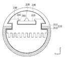
- the tubular LED lighting device 100 includes a substrate 110, a light emitting device 120, a heat sink 130, a cover 140, and a base 150.
- the substrate 110 is a printed circuit board on which a conductive pattern (not shown) is formed.
- the conductive patterns of the substrate 110 are electrically connected to the light emitting device 120.
- the substrate 110 according to the embodiment of the present invention has a long length according to the shape of the long cover 140.
- the light emitting device 120 is mounted on one surface of the substrate 110.
- the light emitting device 120 may include an LED chip (not shown) and may include a phosphor (not shown).
- the light emitting device 120 may generate light of various colors including white light by using a combination of an LED chip and a phosphor.
- 1 to 3 illustrate the plurality of light emitting devices 120 mounted on the substrate 110. However, the number of light emitting devices 120 mounted on the substrate 110 may be changed by a person skilled in the art.
- the heat sink 130 is for heat dissipation of the light emitting device 120 and the substrate 110.
- the heat sink 130 includes a substrate fixing part 131, a groove part 133, and a heat dissipation fin 135.
- the substrate fixing part 131 is formed on one surface of the heat sink 130 on which the substrate 110 is seated, and is formed in a form that surrounds both sides of the substrate 110 on which the substrate 110 is seated. In addition, the substrate fixing part 131 is formed long along the longitudinal direction of the heat sink 130.
- One surface 132 of the substrate fixing part 131 increases in height from the inner side of the heat sink 130 on which the substrate 110 is mounted to the outer side. That is, one surface 132 of the substrate fixing part 131 is formed to have a predetermined angle.
- one surface 132 of the substrate fixing part 131 becomes an upper surface with reference to FIG. 1.
- the predetermined angle is an angle that can prevent the light emitted from the light emitting device 120 from being blocked by the substrate fixing part 131.
- the tubular LED lighting device 100 is capable of high-efficiency light emission by the substrate fixing part 131 formed as described above.
- the groove 133 is formed on both side surfaces of the heat sink 130.
- the groove 133 is formed in the form of a recess formed inwardly of the heat sink 130.
- the groove 133 has a shape corresponding to the protrusion 141 of the cover 140.
- the groove 133 is formed at a position corresponding to the protrusion 141 of the cover 140. The protrusion 141 of the cover 140 is inserted into the groove 133 formed as described above, and thus the heat sink 130 and the cover 140 are coupled to each other.
- the heat dissipation fin 135 is formed under the heat sink 130.
- a plurality of heat dissipation fins 135 may be formed.
- the heat dissipation fin 135 formed as described above expands the area where the heat sink 130 and air contact to improve the heat dissipation performance of the heat sink 130.
- the structure of the heat dissipation fin 135 may be variously changed according to a selection by those skilled in the art.
- Side surfaces of the heat sink 130 are formed to correspond to the inner wall of the cover 140. 1 to 3, since the cover 140 is cylindrical, the inner wall of the cover 140 is curved. Accordingly, the side surface of the heat sink 130 also has a curved shape. Such a structure can minimize the separation distance between the cover 140 and the heat sink 130. As the spacing between the cover 140 and the heat sink 130 is minimized, the heat sink 130 may easily emit heat of the light emitting device 120 and the substrate 110 to the outside through the cover 140. Therefore, the heat radiation performance of the tubular LED lighting device 100 is improved.
- one end of the heat dissipation fin 135 is also formed along the inner wall of the cover 140, as shown in the figure, it can emit heat to the outside through the cover 140.
- the cover 140 is formed to surround the heat sink 130, the substrate 110, and the light emitting device 120. That is, the cover 140 has a heat sink 130, a substrate 110, and a light emitting device 120 therein.
- the cover 140 is formed with a protrusion 141.
- the protrusion 141 is formed to protrude from the inner wall of the cover 140 into the inner space.
- the protrusion 141 is inserted into the grooves 133 formed on both side surfaces of the heat sink 130.
- the cover 140 is formed of a resin or glass material having transparency.
- at least a portion of the cover 140 is formed of pure polymethylmethacrylate (PMMA) material.
- PMMA polymethylmethacrylate
- pure PMMA is free of impurities or other materials added to the PMMA. That is, the cover 140 may be formed entirely of pure PMMA material.
- the cover 140 may be formed of a pure PMMA material.
- the portion of the cover 140, which is a pure PMMA material includes a region through which light of the light emitting device passes. PMMA has a higher light transmittance with a lower concentration of impurities or other materials. Therefore, when the portion of the cover 140 that transmits light of the light emitting device is formed of pure PMMA, light transmittance can be improved.
- the cover 140 is transparent.
- the color of the cover 140 is not limited to being transparent.
- Cover 140 may be translucent or colored.
- Base 150 is coupled to both ends of the cover 140, respectively.
- a cover insertion groove 151 corresponding to an end of the cover 140 is formed in the base 150.
- One end and the other end of the cover 140 are respectively inserted into the cover insertion groove 151 of the base 150, whereby the cover 140 and the base 150 are coupled.
- the cover 140 and the base 150 are fixed to each other by using the screw 160.
- One end of the screw 160 is located inside the base 150, and the other end is located inside the cover 140.
- the cover 140 and the base 150 may be fixed by using an adhesive.
- the present invention is not limited to using a screw or an adhesive.
- the method for fixing the cover 140 and the base 150 may be applied to any method known in the art.
- the sealing member 170 is inserted into an empty space between the screw 160 and the outside of the tubular LED lighting device 100.
- the sealing member 170 prevents moisture from penetrating from the outside to the inside of the tubular LED lighting device 100.
- the sealing member 170 is formed of an elastic material and may be a rubber packing.
- the sealing member 170 may be omitted at the choice of those skilled in the art.
- 4 to 6 is an exemplary view showing a tubular LED lighting apparatus according to a second embodiment of the present invention.
- 4 is a component diagram of a tubular LED lighting apparatus according to a second embodiment of the present invention.
- 5 is a cross-sectional view of the tubular LED lighting apparatus according to the second embodiment of the present invention.
- 6 is a side cross-sectional view of the tubular LED lighting apparatus according to the second embodiment of the present invention.
- the tubular LED lighting device 200 includes a substrate 210, a light emitting device 120, a heat sink 130, a cover 140, and a base 250.
- the substrate 210, the light emitting device 120, and the heat sink 130 are disposed in the cover 140.
- the substrate 210 is fixed to the substrate fixing part 131 formed on one surface of the heat sink 130.
- the light emitting device 120 is mounted on one surface of the substrate 210.
- the base 250 is coupled to both ends of the cover 140.
- a cover insertion groove 251 is formed in the base 250. One end portion and the other end portion of the cover 140 are respectively inserted into the cover insertion groove 251 of the base 250, thereby engaging the base 250.
- one end 211 of the substrate 210 penetrates inside the base 250.
- a hole (not shown) penetrating the inside is formed in the base 250 that is coupled to one end of the cover 140.
- One end 211 of the substrate 210 penetrates the base 250 through the hole and is positioned inside the base 250.
- a power pad 280 is formed at one end 211 of the substrate 210 positioned inside the base 250.
- the power pad 280 includes a first power pad 281 and a second power pad 282.
- one of the first power pad 281 and the second power pad 282 is connected to the positive power of the external power supply, the other is connected to the negative power. 4 to 6, both the first power pad 281 and the second power pad 282 are formed on one surface of the substrate 210 side by side.
- the power pad 280 formed as described above is electrically connected to the light emitting device 120 through a conductive pattern (not shown) formed on the substrate 210.
- the power pad 280 is connected to an external power supply device (not shown). That is, the power pad 280 located inside the base 250 electrically connects an external power supply device (not shown) and the light emitting device 120.
- the other end of the cover 140 and the coupling of the base 250 is the same as FIG.
- the conventional base heat radiation fin insertion and wire bonding process can be omitted, the process is simplified.
- FIG. 7 to 9 are exemplary views showing the tubular LED lighting apparatus according to the third to fifth embodiments of the present invention.
- FIGS. 4 to 6 a portion of the substrate 210, 510 located inside the base 250 is shown. Portions of the illustrated substrates 210 and 510 correspond to one ends 211 of the substrate 210 described in the second embodiment of FIGS. 4 to 6.
- FIG. 7 is an exemplary view showing a tubular LED lighting apparatus according to a third embodiment of the present invention.
- a power pad 280 is formed on one surface and the other surface of the substrate 110, respectively.
- the first power pad is formed on one surface of the substrate 110
- the second power pad is formed on the other surface of the substrate 110.
- FIG 8 is an exemplary view showing a tubular LED lighting apparatus according to a fourth embodiment of the present invention.
- a power pad 280 is formed on one end surface of the substrate 110. That is, the first power pad 281 and the second power pad 282 are formed to be parallel to one end surface of the substrate 110.
- FIG 9 is an exemplary view showing a tubular LED lighting apparatus according to a fifth embodiment of the present invention.
- the tubular LED lighting apparatus 500 is formed such that one end of the substrate 510 has a separation space. That is, the substrate 510 has a structure in which one end is divided into two. A power pad 280 is formed at a cracked portion of the substrate 510. More specifically, as shown in FIG. 9, the first power pad 281 and the second power pad 282 are formed to be respectively disposed at the divided portions of the substrate 510.
- the structure of the substrate and the power pad has been described with reference to FIGS. 4 through 9.
- the structure of the substrate and the power pad is not limited to the above embodiments.
- One end of the substrate may be changed to a structure advantageous for connection with an external power supply device.
- the position and structure in which the power pad is formed may also be changed to advantageously make an electrical connection with an external power supply.
- 10 and 11 are exemplary views showing a tubular LED lighting apparatus according to a sixth embodiment of the present invention.
- 10 is a side cross-sectional view of a tubular LED lighting apparatus according to a sixth embodiment of the present invention.
- 11 is a cross-sectional view of the tubular LED lighting apparatus according to the sixth embodiment of the present invention.
- tubular LED lighting apparatus 600 The difference between the tubular LED lighting apparatus 600 and the tubular LED lighting apparatus 600 according to the second embodiment will now be described. For a description of the omitted configuration, refer to the second embodiment.
- one end 211 and the other end of the substrate 210 are located inside the base 250. However, like other embodiments, only one end of the substrate 210 may be located inside the base 250.
- a power pad 280 is formed at one end 211 of the substrate 210.
- the tubular LED lighting device 600 includes a connector 690.
- a conductive pattern is formed on the connector 690.
- all of one surface and the other surface of the connector 690 may be formed of a conductive material.
- one surface and the other surface of the connector 690 should be insulated from each other.
- conductive patterns may be formed in one side and the other side of the connector 690 and the inside of the connector 690. The conductive patterns formed on one side and the other side of the connector 690 are formed at one end and the other end of the connector 690, respectively.
- One end of the connector 690 contacts the power pad 280 of the substrate 210.
- the conductive patterns electrically connected to the first power pad 281 and the second power pad 282 are formed to be insulated from each other.
- the other end of the connector 690 is exposed to the outside of the base 250.
- the other end of the connector 690 exposed to the outside of the base 250 is connected to an external power supply (not shown).
- the board 210 and the external power supply device are electrically connected through the connector 690.
- FIGS. 12 to 14 are exemplary views showing a tubular LED lighting apparatus according to the seventh to ninth embodiments.
- the configuration of the tubular LED lighting apparatuses 700, 800, and 900 according to the seventh to ninth embodiments will be described mainly based on differences from the tubular LED lighting apparatus according to the sixth embodiment. See also.
- FIG. 12 is an exemplary view showing a tubular LED lighting apparatus according to the seventh embodiment.
- a first power pad 281 and a second power pad 282 are formed on one surface of a substrate 210.
- the connector 790 also includes a first connector 791 and a second connector 792.
- the first connector 791 is in contact with the first power pad 281 to be electrically connected to each other.
- the second connector 792 is in contact with the second power pad 282 to be electrically connected to each other.
- the first connector 791 and the second connector 792 may be formed of a conductive material.
- a conductive pattern for electrical connection between the substrate 210 and an external power supply device may be formed in the first connector 791 and the second connector 792.
- FIG. 13 is an exemplary view showing a tubular LED lighting apparatus according to an eighth embodiment.
- a power pad 280 is formed on one surface and the other surface of the substrate 210, respectively.
- a first power pad is formed on one surface of the substrate 210
- a second power pad is formed on the other surface of the substrate 210.
- the first connector 791 is in contact with the first power pad to be electrically connected to each other.
- the second connector 792 is in contact with the second power pad to be electrically connected to each other.
- the first connector 791 and the second connector 792 may be formed of a conductive material.
- a conductive pattern for electrical connection between the substrate 210 and an external power supply device may be formed in the first connector 791 and the second connector 792.
- FIG 14 is an exemplary view showing a tubular LED lighting apparatus according to the ninth embodiment.
- power pads 280 are formed on both side surfaces of the substrate 210.
- a first power pad is formed on one side of the substrate 210 and a second power pad is formed on the other side.
- the first connector 791 is in contact with the first power pad to be electrically connected to each other.
- the second connector 792 is in contact with the second power pad to be electrically connected to each other.
- the first connector 791 and the second connector 792 may be formed of a conductive material.
- a conductive pattern for electrical connection between the substrate 210 and an external power supply device may be formed in the first connector 791 and the second connector 792.
- the power pads may have various structures at one end of the substrate located inside the base, and may be formed at various positions.
- the connector also has various structures, and can be disposed at various positions.
- 15 is an exemplary view showing a tubular LED lighting apparatus according to a tenth embodiment.
- Covers (140 of FIGS. 1 to 14) of the lighting apparatus according to the first to ninth embodiments of the present invention have been described as being formed of a light transmitting material.
- the present invention is not limited to the entire cover (140 of FIG. 1S to FIG. 14) made of a light-transmissive material.
- the cover 1040 of the tubular LED lighting apparatus 1000 is a mixture of a light transmitting material and a non-light transmitting material.
- the cover 1040 is divided into a first cover 1041 and a second cover 1042.
- the first cover 1041 is a portion of the cover 1040 positioned above the protrusion 141 based on FIG. 15. That is, the first cover 1041 includes a portion through which the light emitted from the light emitting device 120 passes.
- the first cover 1041 is formed of a light transmitting material.
- the first cover 1041 is formed of pure PMMA material.
- the second cover 1042 is a portion located under the protrusion 141 and the protrusion 141 of the cover 1040 based on FIG. 15. That is, the second cover 1042 is a portion of the cover 1040 except for the first cover 1041.
- the second cover 1042 is formed of a non-transparent material.
- the first cover 1041 and the second cover 1042 are divided based on the protrusion 141.
- the reference of the first cover 1041 and the second cover 1042 may not necessarily be the protrusion 141. That is, if the first cover 1041 can pass the light emitted by the light emitting device 120, the reference of the first cover 1041 and the second cover 1042 may be changed according to the choice of those skilled in the art.
- the joining method of the first cover 1041 and the second cover 1042 may be applied to any method known in the art.
- the first cover 1041 and the second cover 1042 may be integrated, and a method of coating a non-transparent material on a portion corresponding to the second cover 1042 may be applied.
- 16 is an exemplary view showing a tubular LED lighting apparatus according to the eleventh embodiment.
- Covers of the lighting apparatus according to the first to ninth embodiments of the present invention has been described as an example of being formed in one color of transparent, translucent or colored.
- the present invention is not limited to the entire cover (140 of FIGS. 1 to 14) formed in one color.
- the cover 1140 may be a mixture of two or more colors of transparent, translucent, and colored.
- the cover 1140 is divided into a first cover 1141 and a second cover 1142.
- the first cover 1141 is a portion of the cover 1140 positioned above the protrusion 141 based on FIG. 16.
- the second cover 1142 is a portion of the cover 1140 except for the first cover 1141.
- the first cover 1141 is transparent, and the second cover 1142 is formed to be translucent or colored.
- the color of the first cover 1141 and the color of the second cover 1142 are not limited thereto.
- the first cover 1141 may be translucent or colored, and the second cover 1142 may be transparent.
- the first cover 1141 may be translucent and the second cover 1142 may be colored.
- the first cover 1141 may be colored and the second cover 1142 may be translucent.
- the translucent or colored cover 1140 may coat translucent or colored on the transparent first cover 1141 and the second cover 1142.
- the translucent or colored cover 1140 may be formed by including a material for translucent or colored when forming the first cover 1141 and the second cover 1142.
- the first cover 1141 and the second cover 1142 are divided based on the protrusion 141.
- the reference of the first cover 1141 and the second cover 1142 may not necessarily be the protrusion 141.
- the order of the first cover 1141 and the second cover 1142 may be changed according to the choice of those skilled in the art.
- the first cover 1141 and the second cover 1142 are divided into different colors, and the first cover 1141 and the second cover 1142 are separated from each other. There is no need. That is, the first cover 1141 and the second cover 1142 may be integrated.
- the cover 1140 may be a mixed color.
- the two colors are not necessarily mixed with the cover 1140. Three or more colors may be mixed in the cover 1140.
- the cover of the tenth embodiment (1040 of FIG. 15) and the cover of the eleventh embodiment (1140 of FIG. 16) may be mixed with each other. That is, the translucent first cover 1041 of FIG. 15 and the non-transparent second cover 1042 of FIG. 15 may each include at least one color of transparent, translucent, and colored.
- 17 is a diagram illustrating an ultraviolet lamp 2100 according to an embodiment of the present invention.
- 18 is a side view illustrating the ultraviolet lamp 2100 of FIG. 17.
- an ultraviolet lamp 2100 may include a lamp tube 2110, a printed circuit board 2120, at least one ultraviolet light emitting device 2130, bases 2141 and 2142, and at least one power pin. 2151).
- the lamp tube 2110 includes an upper cover and a lower cover integrally formed with the upper cover.
- the lamp tube 2110 extends in the X direction and defines an interior space of the ultraviolet lamp 2100.
- the lamp tube 2110 has a height in the Z direction.
- the lamp tube 2110 may have a cylindrical shape as shown in FIG. 17.
- the upper cover 2111 is formed of a transparent material.
- the upper cover 2111 includes polymethyl methacrylate (PMMA) and / or quartz.
- the lower cover 2112 may be formed of an opaque material to cover the space corresponding to the lower cover 2112 in the inner space of the lamp tube 2110.
- Lower cover 2112 may comprise polymethylmethacrylate and / or quartz.
- the lower cover 2112 may further include at least one of a pigment, a filler, and the like.
- the printed circuit board 2120 extends in the X direction and has a width in the Y direction.
- the printed circuit board 2120 is fixed in the lamp tube 2110.
- the printed circuit board 2120 drives the at least one ultraviolet light emitting device 2130 based on the power received through the power pin 2215.
- At least one ultraviolet light emitting device 2130 is disposed on the printed circuit board 2120.
- ten ultraviolet light emitting devices are illustrated as arranged on the printed circuit board 2120 along the X direction.
- the ultraviolet light emitting device 2130 faces the upper cover 2111.
- the ultraviolet light emitting device 2130 is configured to emit ultraviolet light under the control of the printed circuit board.
- the ultraviolet light emitting device 2130 will be fixed so that its ultraviolet light will emit in the direction of the transparent top cover.
- the ultraviolet light emitting device 2130 may be an ultraviolet light emitting diode.
- Bases 2141 and 2142 are fixed to both ends of the lamp tube 2110.
- the bases 2141 and 2142 may block the inside of the lamp tube 2110 from the outside.
- At least one power pin 2215 is fixed to the bases 2141 and 2142.
- the power pin 2215 is connected to an external connector (not shown) to receive power for driving the printed circuit board 2120.
- the external connector provides the DC power
- the printed circuit board 2120 will receive the DC power through the power pin 2215.
- the ultraviolet lamp 2100 may further include a power supply configured to convert AC power received through the power pin 2151 to DC power. The power supply will provide the converted direct current power to the printed circuit board 2120.
- the bases 2141 and 2142 may include polycarbonate (PC).
- 19 is a cross-sectional view of the ultraviolet lamp 2100 along the line II ′ of FIG. 17.
- the ultraviolet lamp 2100 further includes a heat sink 2160.
- the heat sink 2160 is configured to dissipate heat generated when the printed circuit board 2120 is driven.
- the lower portion of the heat sink 2160 may include a plurality of irregularities as shown in FIG. 19.
- the plurality of recesses and protrusions causes the lower portion of the heat sink 2160 to have a large surface area, and thus the heat sink 2160 can efficiently dissipate heat.
- Heat sink 2160 is secured to lamp tube 2110.
- the upper cover 2111 and the lower cover 2112 each include a protrusion 2111_1 and a protrusion 2112_1 protruding toward the inner space, and the heat sink 2160 is provided at the protrusions 2111_1 and 2112_1. Can be fixed.
- a groove 2161 may be formed on the heat sink 2160. As the printed circuit board 2120 is located in the groove 2161, the heat sink 2160 will support the printed circuit board 2120.
- the heat sink 2160 may include at least one protrusion 2162 protruding from the top of the groove 2161 in the Y direction or the direction opposite to the Y direction. By the protrusions 2162, the printed circuit board 2120 may be effectively fixed to the heat sink 2160.
- 20A is a graph showing a change in transmittance of the upper cover 2111 including polymethylmethacrylate according to the change of the wavelength of light.
- the horizontal axis represents wavelength in nanometers (nm) and the vertical axis represents transmittance.
- the top cover 2111 including polymethyl methacrylate at 200 nm has a transmittance of 0%. Near about 300 nm, the transmittance of the top cover 2111 increases rapidly. At about 340 nm, the transmittance of the upper cover 2111 is higher than 90%, and at a wavelength of 360 nm or more, the transmittance of the upper cover 2111 is stably maintained at a value higher than 90%.
- the transmittance of the top cover 2111 at 400 nm, 500 nm, 600 nm, 700 nm, 800 nm, 900 nm, 1000 nm, and 1100 nm has a value higher than 90%. It can be understood that polymethylmethacrylate has a critical significance at about 360 nm.
- the ultraviolet light emitting device 2130 emits ultraviolet rays having a wavelength of 360 nm or more toward the upper cover 2111, and the upper cover 2111 includes polymethyl methacrylate.
- the upper cover 2111 may transmit the ultraviolet ray with high transmittance.
- Ultraviolet rays can generally have a wavelength region of about 100-400 nm.
- the ultraviolet light emitting device 2130 may emit ultraviolet light having a wavelength selected from a wavelength range of 360 nm to 400 nm.
- polymethyl methacrylate may have a material property that is strained at a relatively low temperature.
- the possibility of deformation of the top cover 2111 due to heat is problematic when ultraviolet rays having a wavelength of 360 nm or more are transmitted to the top cover 2111 including polymethyl methacrylate.
- FIG. 20B is a graph showing a change in transmittance of the upper cover 2111 with time when the upper cover 2111 including polymethyl methacrylate transmits ultraviolet rays having a wavelength of 360 nm.
- FIG. 21 is a graph showing a change in transmittance of the upper cover 2111 having a diffusing agent according to a change in wavelength of light. 20B and 21, the horizontal axis represents time and the vertical axis represents transmittance.
- the transmittance of the top cover 2111 is maintained at about 90%.
- the time when the upper cover 2111 is exposed to the corresponding ultraviolet rays is 0 hours, 250 hours, 500 hours, 750 hours, 1000 hours, 2000 hours, and 3000 hours
- the transmittance of the upper cover 2111 is about. 90%.
- the transmittance of the top cover 2111 may vary from about 5% to 10%.
- the transmittance is maintained high, which may mean that the upper cover 2111 is not deformed even if the upper cover 2111 is continuously exposed to the ultraviolet rays.
- the color of the upper cover 2111 will not change or cracks will occur in the upper cover 2111. This may mean that heat is not easily generated in the upper cover 2111 when the ultraviolet rays are used. It can be understood that this is due to the efficient transmission of the upper cover 2111 without absorbing the corresponding ultraviolet rays.
- the polymethyl methacrylate has physical properties that are deformed at a relatively low temperature
- the upper cover 2111 containing polymethyl methacrylate is provided when an ultraviolet light emitting device that emits ultraviolet rays having a wavelength of 360 nm or more is provided. May not be modified.
- the upper cover 2111 transmits ultraviolet rays having a wavelength of 360 nm or more with high transmittance, but will not be deformed even if exposed to the ultraviolet rays for a long time.
- the top cover 2111 may include no diffusion agent or a small amount of diffusion agent for diffusing light.
- a diffusing agent may be included in the tube of the lamp that emits visible light. By the diffusing agent, the visible light transmitted through the tube is diffused and the uniformity of the visible light is increased.
- the top cover 2111 includes a diffusing agent. Ultraviolet rays having a wavelength of 360 nm or more may be absorbed and scattered by the diffusing agent such that transmittance of the upper cover 2111 may be reduced. Referring to FIG. 21, the transmittance of the upper cover 2111 is less than 10% at 360 nm and has a transmittance of 90% at 400 nm or more.
- the upper cover 2111 has a high transmittance with respect to visible light when it includes a diffusing agent, but has a low transmittance with ultraviolet rays having a wavelength of 360 nm to 400 nm.
- the upper cover 2111 may not include a diffusion agent or may include a small amount of the diffusion agent. Accordingly, the transmittance for ultraviolet light having a wavelength of 360 nm or more of the upper cover 2111 will be kept high as described with reference to FIG. 20B. Furthermore, since absorption and refraction of ultraviolet rays by the diffusing agent do not occur, the possibility of deformation of the upper cover 2111 due to heat can be reduced.
- the top cover 2111 may include no impact modifier, for example an acrylic rubber, or a small amount of impact modifier. Without absorption of ultraviolet light by the impact modifier, the transmittance for ultraviolet light with a wavelength greater than or equal to 360 nm of the top cover 2111 will remain high as described with reference to FIG. 20B.
- top cover 2111 includes pure polymethylmethacrylate (clear PMMA).
- FIG. 22 is a cross-sectional view of an ultraviolet lamp 2100 according to another embodiment of the present invention.
- a printed circuit board 2220, an ultraviolet light emitting device 2230, a heat sink 2260, and a power supply 2270 are provided inside the upper cover 2211 and the lower cover 2212. Is provided.
- the top cover 2211 has a high transmittance without deformation for ultraviolet light having a wavelength of 360 nm. Accordingly, the internal structure of the lamp tube may be changed such that the heat sink 2260 is located at a high height H1 such that the distance between the ultraviolet light emitting device 2230 and the upper cover 2211 is shorter than in the embodiment of FIG. 19. Can be.
- the heat sink 2260 may be located at a position higher than or equal to the height H1.
- the height H1 may be higher than the height H2 corresponding to the radius of the lamp tube (see 2110 of FIG. 17). Accordingly, an area in which the power supply device 2270 is disposed between the heat sink 2260 and the lower cover 2212 may be secured.
- the upper cover 2211 may include polymethyl methacrylate and / or quartz, but may be formed to be transparent
- the lower cover 2212 may include polymethyl methacrylate and / or quartz, but may be formed to be opaque. have.
- Heat sink 2260 may be secured to the lamp tube in a variety of ways.
- the lower cover 2212 includes first and second protrusions 2212_1 and 2212_2 protruding into the inner region of the lamp tube, and the heat sink 2260 is the first. And the second protrusions 2212_1 and 2212_2.
- the power supply device 2270 is configured to convert AC power from the outside into DC power and provide the converted DC power to the printed circuit board 2220.
- the power supply 2270 may be a switched mode power supply (SMPS).
- SMPS switched mode power supply
- 23 is a cross-sectional view of an ultraviolet lamp 2100 according to another embodiment of the present invention.
- 24 is an exploded perspective view illustrating a printed circuit board 2320, ultraviolet light emitting devices 2330, a heat sink 2360, and a flame retardant layer 2380.
- a printed circuit board 2320, an ultraviolet light emitting device 2330, a heat sink 2360, and a flame resisting layer 2380 are disposed inside the upper cover 2311 and the lower cover 2312. Is provided.
- the polymethylmethacrylate included in the top cover 2311 may have physical properties that are modified at a relatively low temperature. Meanwhile, the printed circuit board 2320 may generate a spark, a flame, or the like during driving.
- a flame resistant layer 2380 is provided between the printed circuit board 2320 and the top cover 2311.
- the flame retardant layer 2380 may be disposed on the printed circuit board 2320.
- the flame retardant layer 2380 includes a material that is difficult to burn.
- the flame retardant layer 2380 may protect the upper cover 2311 from sparks and flames generated from the printed circuit board 2320.
- a groove 2361 may be formed in the heat sink 2360.
- the heat sink 2360 may include at least one protrusion 2362 protruding from the top of the groove 2361 in a Y direction or a direction opposite to the Y direction.
- Printed circuit board 2320 and flame retardant layer 2380 may be received in groove 2361 and secured by protrusion 2362.
- the flame retardant layer 2380 includes at least one hole 381.
- Each hole 381 may correspond to each ultraviolet light emitting device 2330 on the printed circuit board 2320.
- the ultraviolet light emitting device 2330 passes through the hole 381. After attachment, the ultraviolet light emitting device 2330 will penetrate through the flame retardant layer 2380 toward the top cover 2311.
- Printed circuit board 2320 and flame retardant layer 2380 are secured in groove 2361.
- 25 is a cross-sectional view of an ultraviolet lamp 2100 according to another embodiment of the present invention.
- a printed circuit board 2420, an ultraviolet light emitting device 2430, a heat sink 2460, and a flame retardant layer 2480 are provided inside the upper cover 2411 and the lower cover 2412.
- Printed circuit board 2420 is located in groove 2241 formed in heat sink 2460.
- the flame retardant layer 2480 may be provided to cover the top of the heat sink 2460 and the printed circuit board 2420.
- an adhesive may be used to fix the flame retardant layer 2480 on top of the heat sink 2460 and on the printed circuit board 2420.
- FIG. 26 is a cross-sectional view of the ultraviolet lamp 2100 along the line II-II ′ of FIG. 17.
- a printed circuit board 2120, an ultraviolet light emitting device 2130, and a heat sink 2160 are provided inside the upper cover 2111 and the lower cover 2112.
- the base 2141 is fixed to one end of the lamp tube 2110 (see FIG. 17).
- the base 2141 may include grooves for receiving the upper cover 2111 and the lower cover 2112 as shown in FIG. 26.
- the base 2141 may include a support portion 2141_1 protruding in the X direction to support the heat sink 2160.
- the ultraviolet light emitting device 2130 may have a predetermined directivity range RG.
- the ultraviolet light emitting device 2130 may emit ultraviolet light within a directivity angle of 120 degrees.
- the ultraviolet light emitting device 2130 may be positioned such that the base 2141 is positioned outside the directivity range RG.
- the ultraviolet light emitting device 2130 may be spaced apart from the base 2141 by a specific distance such that the base 2141 is positioned outside the directivity range RG.
- the base 2141 may include an ultraviolet stabilizer.
- the UV stabilizer can include at least one of an absorbent, a quencher, a Hindered Amine Light Stabilizer (HALS), and the like.
- FIG. 27 is a diagram illustrating a modified embodiment 2500 of the ultraviolet lamp 2100 of FIG. 17.
- 28 is a cross-sectional view of the ultraviolet lamp 2500 of FIG. 27.
- a portion of the ultraviolet lamp 2500 is shown in FIGS. 27 and 28.
- the lamp tube 2510 includes an upper cover 2511 and a lower cover 2512.
- the upper cover 2511 and the lower cover 2512 are configured similarly to the upper cover 2111 and the lower cover 2112 described with reference to FIGS. 17 and 18. Duplicate explanations will be omitted below.
- the base 2551 is fixed to the end of the lamp tube 2510.
- the base 2541 may include a support 2551_1 configured to support the heat sink 2560.
- the ultraviolet light emitting device 2530 is disposed on the printed circuit board 2520.
- the printed circuit board 2520 may be disposed on the heat sink 2560 and may include a protrusion 2521 extending from the inner space of the lamp tube 2510 and penetrating the base 2551.
- the shape of the protrusion 2521 will be formed to accommodate an external connector for providing power.
- the ultraviolet lamp 2500 will receive power through the protrusion 2521.
- the printed circuit board 2520 may receive the DC power through the protrusion 2521.
- the ultraviolet lamp 2500 may further include a power supply (see 2270 in FIG. 22) configured to convert AC power received through the protrusion 2521 into DC power. . The power supply will provide the converted direct current power to the printed circuit board 2520.
- 29 is a cross-sectional view of an ultraviolet lamp 2100 according to another embodiment of the present invention.
- the ultraviolet lamp 2100 further includes a flame retardant layer 2180.
- the flame retardant layer 2180 is disposed on the inner surface of the lamp tube 2110.
- the printed circuit board 2120, the ultraviolet light emitting device 2130, and / or the heat sink 2160 may generate and / or transfer heat, and the heat may be transferred to the lamp tube 2110.
- a flame retardant layer 2180 may be further provided on at least a portion of an inner surface of the lamp tube 2110. Accordingly, deformation or burning of the lamp tube 2110 and / or the ultraviolet lamp 2100 can be prevented.
- the flame retardant layer 2180 may be disposed on the entire inner surface of the lamp tube 2110. In another embodiment, the flame retardant layer 2180 may be disposed on a portion of the inner surface of the lamp tube 2110.
- the flame retardant layer 2180 may include fluorine.
- FIG. 30 is a cross-sectional view of an ultraviolet lamp 2100 according to another embodiment of the present invention.
- the flame retardant layer 2190 may surround at least a portion of an outer surface of the lamp tube 2110. In an embodiment, the flame retardant layer 2190 may be disposed on the entire outer surface of the lamp tube 2110. In another embodiment, the flame retardant layer 2190 may be disposed on a portion of the outer surface of the lamp tube 2110. Accordingly, deformation or burning of the lamp tube 2110 and / or the ultraviolet lamp 2100 can be prevented. In addition, the flame retardant layer 2190 may surround the lamp tube 2110 and support the lamp tube 2110 to prevent the lamp tube 2110 from being scattered by an external impact. For example, this advantage is more pronounced when the lamp tube 2110 has good cracking properties, including, for example, quartz.
- FIG. 31 is a flowchart for explaining a method of manufacturing the lamp tube 2110 of FIG. 17.
- step S110 a first raw material corresponding to the upper cover 2111 (see FIG. 18) and a second raw material corresponding to the lower cover 2112 (see FIG. 18) are prepared.
- the first raw material and the second raw material may be provided to different hoppers, respectively.
- the first raw material includes polymethyl methacrylate and / or quartz.
- the first raw material may include no diffusion agent or may include a small amount of diffusion agent.
- the first raw material may include no impact modifier or a small amount of impact modifier.
- the second raw material may comprise polymethylmethacrylate and / or quartz and materials for the lower cover 2112 to be colored, for example pigments, fillers, and the like. .
- step S120 the first raw material is melted to produce a first melt, and the second raw material is melted to produce a second melt.
- the first melt and the second melt will each be produced in different cylinders. From each hopper, the corresponding raw material will be supplied to the cylinder. In the cylinder, the feedstock supplied will be transported, melted, and compressed at an appropriate pressure to produce a melt.
- step S130 the first melt and the second melt is passed through one mold.
- the first melt and the second melt transported through different cylinders will pass through one mold.
- the top cover and the bottom cover may be molded according to a profile extrusion process.
- the mold can have any of a variety of shapes.
- the mold may have shapes corresponding to the upper cover 2111 and the lower cover 2112 shown in FIG. 19.
- the upper cover 211 and the lower cover 212 shown in FIG. It may have a shape corresponding to the.
- the transparent upper cover 2111 and the opaque lower cover 2112 may be integrally formed by passing the first melt and the second melt through one mold.
- step S140 the upper cover 2111 and the lower cover 2112 are cooled to provide a lamp tube 2110.
- the upper cover 2111 and the lower cover 2112 may be cooled by the coolant to maintain the molded shape according to the mold.
- lamp tube 2110 may be cut to have an appropriate length.
- the printed circuit board 2120 (see FIG. 19), the ultraviolet light emitting device 2130 (see FIG. 19), and the heat sink 2160 (see FIG. 19) will be disposed in the lamp tube 2110.
- the ultraviolet lamp includes an ultraviolet light emitting device that emits ultraviolet rays having a wavelength of 360 nm or more toward the upper cover, and a top cover having polymethyl methacrylate.
- the upper cover will not deform even if exposed to the ultraviolet rays for a long time while transmitting the ultraviolet rays with high transmittance.
- an ultraviolet lamp with improved performance and reliability can be provided.
- the tubular LED lighting apparatus has a shorter separation distance between the heat sink and the cover, thereby improving heat dissipation.
- the tubular LED lighting apparatus according to an embodiment of the present invention is formed so that one end of the substrate on which the electrode is formed is located inside the base, it can be electrically connected to the external power supply without wire bonding. Therefore, the tubular LED lighting device can simplify the process by eliminating wire bonding, and can prevent defects due to opening and short circuit due to wire bonding.
Landscapes
- Engineering & Computer Science (AREA)
- General Engineering & Computer Science (AREA)
- Physics & Mathematics (AREA)
- Microelectronics & Electronic Packaging (AREA)
- Optics & Photonics (AREA)
- Non-Portable Lighting Devices Or Systems Thereof (AREA)
- Fastening Of Light Sources Or Lamp Holders (AREA)
Abstract
The present invention relates to a tube-shaped LED lighting device. A tube-shaped LED lighting device according to an embodiment comprises: a substrate; a light emitting element mounted on the substrate; a heat sink having one surface on which the substrate is stably placed and having both opposite side surfaces on which inwardly concave groove portions are formed; a cover housing the heat sink, the substrate, and the light emitting element and including protrusion portions which protrude from an inner wall of the cover and are inserted into the groove portions; and bases coupled respectively to both opposite ends of the cover, wherein the opposite side surfaces of the heat sink have a morphology corresponding to that of the inner wall of the cover.
Description
본 발명은 튜브형 엘이디 조명 장치에 관한 것이다.The present invention relates to a tubular LED lighting device.
일반적으로 엘이디(LED; Light Emitting Diode)는 화합물에 전류를 흘려 빛을 발산하는 반도체 소자이다. 엘이디는 수은을 사용하지 않아 친환경적이고, 고체 디바이스이어서 수명이 길며, 소비 전력이 낮아 새로운 광원으로 주목받고 있다.In general, an LED (Light Emitting Diode) is a semiconductor device that emits light by flowing a current through the compound. LED does not use mercury, so it is eco-friendly, and it is a solid device, which has a long life and low power consumption.
이러한 엘이디를 광원으로 하는 다양한 조명 장치가 개발되고 있으며, 전구용 소켓(Receptacle)에 장착 가능하게 전구식 전원 연결부가 구비된 엘이디 조명 장치가 호응을 얻고 있다.Various lighting apparatuses using such LEDs as light sources have been developed, and LED lighting apparatuses equipped with bulb-type power connection parts that can be mounted in a socket for a light bulb (Receptacle) have gained popularity.
엘이디는 점등시 열이 발생된다는 문제점이 있다. 엘이디는 방열이 원활하게 되지 못할 경우 수명이 단축되고 조도가 떨어진다. 엘이디 점등이 원활하게 이루어지는 온도 상한선은 60℃ 내외로, 엘이디 조명 장치의 성능은 방열과 직결된다고 할 수 있다.The LED has a problem that heat is generated when it is turned on. If the LED is not good heat dissipation will shorten the life and light intensity. The upper limit of the temperature at which the LED is turned on smoothly is around 60 ° C., and thus the performance of the LED lighting device is directly related to heat dissipation.
자외선은 일반적으로 100~400 나노미터(nanometer)의 파장 영역을 가지는 광을 의미하며, 가시광선에 비해 높은 에너지를 갖는다. 태양으로부터의 자외선은 자외선A(ultraviolet-A), 자외선 B(ultraviolet-B), 및 자외선 C(ultraviolet-C)로 구분되며, 자외선 C는 오존층에 대부분 흡수되고, 자외선 A 및 자외선 B는 지표면에 도달하는 것으로 알려져 있다.Ultraviolet rays generally refer to light having a wavelength range of 100 to 400 nanometers, and have a higher energy than visible light. Ultraviolet rays from the sun are classified into ultraviolet A (ultraviolet-A), ultraviolet B (ultraviolet-C), and ultraviolet C (ultraviolet-C), and ultraviolet C is mostly absorbed by the ozone layer, and ultraviolet A and ultraviolet B are applied to the surface of the earth. It is known to reach.
자외선은 다양한 분야들에서 활용될 수 있다. 자외선 램프는 램프 튜브 및 램프 튜브 내에서 자외선을 발광하는 발광 장치를 포함한다. 램프 튜브는 자외선에 대한 높은 투과율, 자외선을 장시간 투과할 때 변형되지 않는 물성을 요구한다.Ultraviolet light can be utilized in various fields. The ultraviolet lamp includes a lamp tube and a light emitting device that emits ultraviolet light within the lamp tube. The lamp tube requires high transmittance to ultraviolet rays and properties that do not deform when the ultraviolet rays are transmitted for a long time.
본 발명이 해결하고자 하는 과제는 방열 기능이 향상된 튜브형 엘이디 조명 장치를 제공하는 것이다.The problem to be solved by the present invention is to provide a tube type LED lighting device with improved heat dissipation.
또한, 본 발명이 해결하고자 하는 다른 과제는 와이어 본딩을 생략하여 개방 및 단락에 의한 불량을 방지하는 튜브형 엘이디 조명 장치를 제공하는 것이다.In addition, another problem to be solved by the present invention is to provide a tube-type LED lighting device that prevents defects due to opening and short circuit by omitting wire bonding.
본 출원은 향상된 성능 및 신뢰성을 갖는 자외선 램프 및 그 제조 방법을 제공하기 위한 것이다.The present application is to provide an ultraviolet lamp and a method of manufacturing the same having improved performance and reliability.
본 발명의 실시 예에 따르면, 기판, 기판 상에 실장된 발광 소자, 일면에 기판이 안착되며, 양측면에 내측으로 오목한 홈부가 형성된 히트 싱크, 히트 싱크, 기판 및 발광 소자를 내장하며, 내벽에서 돌출되어 홈부에 삽입되는 돌출부를 포함하는 커버 및 커버의 양단에 결합되는 베이스를 포함하며, 히트 싱크의 양측면의 형태는 커버의 내벽의 형태에 대응하는 튜브형 엘이디 조명 장치가 제공된다.According to an embodiment of the present invention, a substrate, a light emitting device mounted on the substrate, a substrate is mounted on one surface, and a heat sink, a heat sink, a substrate, and a light emitting device formed with recesses inwardly formed on both sides thereof, and protrude from the inner wall. And a base coupled to both ends of the cover, the cover including a protrusion inserted into the groove, and both sides of the heat sink are provided with a tubular LED lighting device corresponding to the shape of the inner wall of the cover.
본 발명의 다른 실시 예에 따르면, 기판, 기판 상에 실장된 발광 소자(Light Emitting Device), 일면에 기판이 안착되며, 양측면에 내측으로 오목한 홈부가 형성된 히트 싱크, 히트 싱크, 기판 및 발광 소자를 내장하며, 내벽에서 돌출되어 홈부에 삽입되는 돌출부를 포함하는 커버 및 커버의 양단에 결합하는 베이스를 포함하며, 기판의 일단은 베이스를 관통하여 베이스의 내부에 위치하는 튜브형 엘이디 조명 장치가 제공된다.According to another embodiment of the present invention, a heat sink, a heat sink, a substrate, and a light emitting device having a substrate, a light emitting device mounted on the substrate, a substrate seated on one surface, and recessed grooves formed on both sides thereof inwardly There is provided a tubular LED lighting device which includes a cover which includes a cover and a base including a protrusion which protrudes from an inner wall and is inserted into a groove, and one end of the substrate penetrates the base and is positioned inside the base.
본 발명의 실시 예에 따른 자외선 램프는, 상부 커버 및 상기 상부 커버와 일체로 형성되는 하부 커버를 포함하는 램프 튜브; 상기 램프 튜브 내에 고정되는 인쇄 회로 기판; 및 상기 인쇄 회로 기판 상에 배치되고 상기 상부 커버에 대향하되, 상기 인쇄 회로 기판의 제어에 따라 구동하는 적어도 하나의 자외선 발광 장치를 포함하되, 상기 적어도 하나의 자외선 발광 장치는 360nm 이상의 파장을 갖는 자외선을 상기 상부 커버를 향해 발광하고, 상기 상부 커버는 폴리메틸메타크릴레이트를 포함한다.An ultraviolet lamp according to an embodiment of the present invention, the lamp tube including an upper cover and a lower cover integrally formed with the upper cover; A printed circuit board fixed in the lamp tube; And at least one ultraviolet light emitting device disposed on the printed circuit board and opposed to the upper cover, and driven under the control of the printed circuit board, wherein the at least one ultraviolet light emitting device has ultraviolet light having a wavelength of 360 nm or more. Emits light toward the upper cover, and the upper cover includes polymethylmethacrylate.
실시 예로서, 상기 자외선 램프는 상기 인쇄 회로 기판과 상기 상부 커버 사이에 배치되는 난연 레이어를 더 포함할 수 있다.In example embodiments, the ultraviolet lamp may further include a flame retardant layer disposed between the printed circuit board and the upper cover.
실시 예로서, 상기 자외선 램프는 상기 램프 튜브 내에 고정되며, 상기 인쇄 회로 기판에 의해 발생되는 열을 방출하도록 구성되는 히트 싱크를 더 포함할 수 있다. 이때, 상기 히트 싱크의 상부에 그루브가 형성되고, 상기 인쇄 회로 기판 및 상기 난연 레이어는 상기 그루브 내에 위치하고, 상기 난연 레이어는 상기 인쇄 회로 기판을 커버할 수 있다.In an embodiment, the ultraviolet lamp may further include a heat sink fixed in the lamp tube and configured to dissipate heat generated by the printed circuit board. In this case, a groove may be formed on the heat sink, the printed circuit board and the flame retardant layer may be located in the groove, and the flame retardant layer may cover the printed circuit board.
실시 예로서, 상기 자외선 램프는 상기 램프 튜브 내에 고정되며, 상기 인쇄 회로 기판에 의해 발생되는 열을 방출하도록 구성되는 히트 싱크를 더 포함할 수 있다. 이때, 상기 히트 싱크의 상부에 그루브가 형성되고, 상기 인쇄 회로 기판은 상기 그루브 내에 위치하고, 상기 난연 레이어는 상기 히트 싱크의 상기 상부 및 상기 인쇄 회로 기판을 커버할 수 있다.In an embodiment, the ultraviolet lamp may further include a heat sink fixed in the lamp tube and configured to dissipate heat generated by the printed circuit board. In this case, a groove is formed on an upper portion of the heat sink, the printed circuit board is positioned in the groove, and the flame retardant layer may cover the upper portion of the heat sink and the printed circuit board.
실시 예로서, 상기 자외선 램프는 상기 인쇄 회로 기판을 지지하며 상기 인쇄 회로 기판에 의해 발생되는 열을 방출하도록 구성되는 히트 싱크; 및 상기 히트 싱크와 상기 하부 커버 사이에 배치되고, 외부로부터의 교류 전원을 직류 전원으로 변환하고 상기 변환된 직류 전원을 상기 인쇄 회로 기판에 제공하도록 구성되는 전원 공급 장치를 포함할 수 있다. 이때, 상기 하부 커버는 상기 폴리메틸메타크릴레이트를 포함하되 불투명하도록 형성될 수 있다.In an embodiment, the ultraviolet lamp includes a heat sink configured to support the printed circuit board and to dissipate heat generated by the printed circuit board; And a power supply disposed between the heat sink and the lower cover and configured to convert AC power from the outside into DC power and provide the converted DC power to the printed circuit board. In this case, the lower cover may include the polymethyl methacrylate, but may be formed to be opaque.
실시 예로서, 상기 자외선 램프는 상기 램프 튜브의 끝단에 고정되는 베이스를 더 포함할 수 있다. 이때, 상기 적어도 하나의 자외선 발광 장치는 소정의 지향 범위 내에서 상기 자외선을 발광하되 상기 베이스가 상기 소정의 지향 범위 밖에 위치하도록 상기 인쇄 회로 기판 상에 위치할 수 있다.In an embodiment, the ultraviolet lamp may further include a base fixed to an end of the lamp tube. In this case, the at least one ultraviolet light emitting device may be positioned on the printed circuit board to emit the ultraviolet light within a predetermined directivity range, but the base is located outside the predetermined directivity range.
실시 예로서, 상기 자외선 램프는 상기 램프 튜브의 끝단에 고정되는 베이스를 더 포함할 수 있다. 이때, 상기 베이스는 자외선 안정제를 포함할 수 있다.In an embodiment, the ultraviolet lamp may further include a base fixed to an end of the lamp tube. In this case, the base may include an ultraviolet stabilizer.
본 발명의 다른 실시 예에 따른 자외선 램프는 상부 커버 및 상기 상부 커버와 일체로 형성되는 하부 커버를 포함하는 램프 튜브; 상기 램프 튜브 내에 고정되는 인쇄 회로 기판; 상기 인쇄 회로 기판 상에 배치되고 상기 상부 커버에 대향하되, 상기 인쇄 회로 기판의 제어에 따라 자외선을 상기 상부 커버 방향으로 발광하는 적어도 하나의 자외선 발광 장치; 및 상기 인쇄 회로 기판과 상기 상부 커버 사이에 배치되는 난연 레이어를 포함할 수 있다. 상기 상부 커버는 폴리메틸메타크릴레이트를 포함할 수 있다.According to another embodiment of the present invention, an ultraviolet lamp includes: a lamp tube including an upper cover and a lower cover integrally formed with the upper cover; A printed circuit board fixed in the lamp tube; At least one ultraviolet light emitting device disposed on the printed circuit board and facing the upper cover, the ultraviolet light emitting device emitting light toward the upper cover in accordance with control of the printed circuit board; And a flame retardant layer disposed between the printed circuit board and the upper cover. The top cover may comprise polymethylmethacrylate.
실시 예로서, 상기 적어도 하나의 자외선 발광 장치는 360nm 이상의 파장을 갖는 자외선을 발광할 수 있다.In an embodiment, the at least one ultraviolet light emitting device may emit ultraviolet light having a wavelength of 360 nm or more.
실시 예로서, 상기 하부 커버는 상기 폴리메틸메타크릴레이트를 포함하되 불투명하도록 형성될 수 있다.In an embodiment, the lower cover may include the polymethylmethacrylate, but may be formed to be opaque.
본 발명의 다른 일면은 자외선 램프의 제조 방법에 관한 것이다. 본 발명의 실시 예에 따른 자외선 램프의 제조 방법은, 제 1 원료 및 제 2 원료를 용융하여 제 1 용융물 및 제 2 용융물을 각각 생성하고; 상기 제 1 용융물 및 상기 제 2 용융물을 하나의 금형에 통과시켜 일체로서 상부 커버 및 하부 커버를 형성하고; 상기 상부 커버 및 상기 하부 커버를 냉각하고; 인쇄 회로 기판 및 상기 인쇄 회로 기판의 제어에 따라 구동하는 적어도 하나의 자외선 발광 장치를 상기 상부 커버 및 상기 하부 커버 내에 배치하는 것을 포함한다. 상기 적어도 하나의 자외선 발광 장치는 상기 상부 커버에 대향하고, 상기 적어도 하나의 자외선 발광 장치는 360nm의 파장을 갖는 자외선을 상기 상부 커버를 향해 발광하고, 상기 상부 커버는 폴리메틸메타크릴레이트를 포함한다.Another aspect of the present invention relates to a method of manufacturing an ultraviolet lamp. According to one or more exemplary embodiments, a method of manufacturing an ultraviolet lamp includes: melting a first raw material and a second raw material to produce a first melt and a second melt; Passing the first melt and the second melt through one mold to integrally form an upper cover and a lower cover; Cooling the upper cover and the lower cover; And disposing at least one ultraviolet light emitting device driven under control of a printed circuit board and the printed circuit board in the upper cover and the lower cover. The at least one ultraviolet light emitting device faces the top cover, the at least one ultraviolet light emitting device emits ultraviolet light having a wavelength of 360 nm toward the top cover, and the top cover comprises polymethylmethacrylate. .
본 발명의 또 다른 실시 예에 따른 자외선 램프는 상부 커버 및 상기 상부 커버와 일체로 형성되는 하부 커버를 포함하는 램프 튜브; 상기 램프 튜브 내에 고정되는 인쇄 회로 기판; 상기 인쇄 회로 기판 상에 배치되고 상기 상부 커버에 대향하되, 상기 인쇄 회로 기판의 제어에 따라 자외선을 상기 상부 커버 방향으로 발광하는 적어도 하나의 자외선 발광 장치; 및 상기 인쇄 회로 기판과 상기 상부 커버 사이에 배치되거나, 상기 램프 튜브의 외면 중 적어도 일부를 감싸는 난연 레이어를 포함한다.According to another embodiment of the present invention, an ultraviolet lamp includes: a lamp tube including an upper cover and a lower cover integrally formed with the upper cover; A printed circuit board fixed in the lamp tube; At least one ultraviolet light emitting device disposed on the printed circuit board and facing the upper cover, the ultraviolet light emitting device emitting light toward the upper cover in accordance with control of the printed circuit board; And a flame retardant layer disposed between the printed circuit board and the upper cover or surrounding at least a portion of an outer surface of the lamp tube.
실시 예로서, 상기 상부 커버는 폴리메틸메타크릴레이트 또는 석영을 포함할 수 있다.In an embodiment, the top cover may include polymethyl methacrylate or quartz.
실시 예로서, 상기 하부 커버는 상기 폴리메틸메타크릴레이트 또는 석영을 포함하되 불투명하도록 형성될 수 있다.In an embodiment, the lower cover may be formed to include the polymethyl methacrylate or quartz but is opaque.
실시 예로서, 상기 난연 레이어는 상기 램프 튜브의 내면 중 적어도 일부에 부착될 수 있다.In an embodiment, the flame retardant layer may be attached to at least a portion of an inner surface of the lamp tube.
본 발명의 실시 예에 따른 튜브형 엘이디 조명 장치는 히트 싱크와 커버 간의 이격 간격이 짧아 방열 기능이 향상된다.The tubular LED lighting device according to the embodiment of the present invention has a shorter separation distance between the heat sink and the cover, thereby improving heat dissipation.
또한, 본 발명의 실시 예에 따른 튜브형 엘이디 조명 장치는 전극이 형성된 기판의 일단이 베이스의 내부에 위치하도록 형성되어, 와이어 본딩 없이 외부의 전원 장치와 전기적으로 연결될 수 있다. 따라서, 튜브형 엘이디 조명 장치는 와이어 본딩의 생략으로 공정이 단순화 되며, 와이어 본딩에 의한 개방 및 단락에 의한 불량을 방지할 수 있다.In addition, the tubular LED lighting apparatus according to an embodiment of the present invention is formed so that one end of the substrate on which the electrode is formed is located inside the base, it can be electrically connected to the external power supply without wire bonding. Therefore, the tubular LED lighting device can simplify the process by eliminating wire bonding, and can prevent defects due to opening and short circuit due to wire bonding.
본 출원에 따르면, 향상된 성능 및 신뢰성을 갖는 자외선 램프 및 그 제조 방법이 제공된다.According to the present application, an ultraviolet lamp having improved performance and reliability and a method of manufacturing the same are provided.
도 1은 본 발명의 제1 실시 예에 따른 튜브형 엘이디 조명 장치의 부품도이다. 1 is a component diagram of a tubular LED lighting apparatus according to a first embodiment of the present invention.
도 2는 본 발명의 제1 실시 예에 따른 튜브형 엘이디 조명 장치의 단면도이다. 2 is a cross-sectional view of the tubular LED lighting apparatus according to the first embodiment of the present invention.
도 3은 본 발명의 제1 실시 예에 따른 튜브형 엘이디 조명 장치의 측단면도이다.3 is a side cross-sectional view of the tubular LED lighting apparatus according to the first embodiment of the present invention.
도 4는 본 발명의 제2 실시 예에 따른 튜브형 엘이디 조명 장치의 부품도이다. 4 is a component diagram of a tubular LED lighting apparatus according to a second embodiment of the present invention.
도 5는 본 발명의 제2 실시 예에 따른 튜브형 엘이디 조명 장치의 단면도이다. 5 is a cross-sectional view of the tubular LED lighting apparatus according to the second embodiment of the present invention.
도 6은 본 발명의 제2 실시 예에 따른 튜브형 엘이디 조명 장치의 측단면도이다.6 is a side cross-sectional view of a tubular LED lighting apparatus according to a second embodiment of the present invention.
도 7은 본 발명의 제3 실시 예에 따른 튜브형 엘이디 조명 장치를 나타낸 예시도이다.7 is an exemplary view showing a tubular LED lighting apparatus according to a third embodiment of the present invention.
도 8은 본 발명의 제4 실시 예에 따른 튜브형 엘이디 조명 장치를 나타낸 예시도이다.8 is an exemplary view showing a tubular LED lighting apparatus according to a fourth embodiment of the present invention.
도 9는 본 발명의 제5 실시 예에 따른 튜브형 엘이디 조명 장치를 나타낸 예시도이다.9 is an exemplary view showing a tubular LED lighting apparatus according to a fifth embodiment of the present invention.
도 10은 본 발명의 제6 실시 예에 따른 튜브형 엘이디 조명 장치의 측단면도이다. 10 is a side cross-sectional view of a tubular LED lighting apparatus according to a sixth embodiment of the present invention.
도 11은 본 발명의 제 6 실시 예에 따른 튜브형 엘이디 조명 장치의 단면도이다.11 is a cross-sectional view of the tubular LED lighting apparatus according to the sixth embodiment of the present invention.
도 12는 제7 실시 예에 따른 튜브형 엘이디 조명 장치를 나타낸 예시도이다.12 is an exemplary view showing a tubular LED lighting apparatus according to the seventh embodiment.
도 13은 제8 실시 예에 따른 튜브형 엘이디 조명 장치를 나타낸 예시도이다.13 is an exemplary view showing a tubular LED lighting apparatus according to an eighth embodiment.
도 14는 제9 실시 예에 따른 튜브형 엘이디 조명 장치를 나타낸 예시도이다.14 is an exemplary view showing a tubular LED lighting apparatus according to the ninth embodiment.
도 15는 제10 실시 예에 따른 튜브형 엘이디 조명 장치를 나타낸 예시도이다.15 is an exemplary view showing a tubular LED lighting apparatus according to a tenth embodiment.
도 16은 제11 실시 예에 따른 튜브형 엘이디 조명 장치를 나타낸 예시도이다.16 is an exemplary view showing a tubular LED lighting apparatus according to the eleventh embodiment.
도 17은 본 발명의 실시 예에 따른 자외선 램프를 보여주는 도면이다.17 is a view showing an ultraviolet lamp according to an embodiment of the present invention.
도 18은 도 17의 자외선 램프를 보여주는 측면도이다.FIG. 18 is a side view illustrating the ultraviolet lamp of FIG. 17.
도 19는 도 17의 I-I'선에 따른 자외선 램프의 단면도이다.19 is a cross-sectional view of the ultraviolet lamp taken along line II ′ of FIG. 17.
도 20a는 빛의 파장의 변화에 따라 폴리메틸메타크릴레이트를 포함하는 상부 커버의 투과율의 변화를 보여주는 그래프이다.20A is a graph showing a change in transmittance of a top cover including polymethylmethacrylate according to a change in wavelength of light.
도 20b는 폴리메틸메타크릴레이트를 포함하는 상부 커버가 360nm의 파장을 갖는 자외선을 투과할 때 시간에 따른 상부 커버의 투과율의 변화를 보여주는 그래프이다.20B is a graph showing the change in transmittance of the top cover with time when the top cover including polymethyl methacrylate transmits ultraviolet rays having a wavelength of 360 nm.
도 21은 빛의 파장의 변화에 따라 확산제를 갖는 상부 커버의 투과율의 변화를 보여주는 그래프이다.FIG. 21 is a graph showing the change in transmittance of the upper cover with a diffusing agent according to the change in wavelength of light.
도 22은 본 발명의 다른 실시 예에 따른 자외선 램프의 단면도이다.22 is a cross-sectional view of an ultraviolet lamp according to another embodiment of the present invention.
도 23은 본 발명의 또 다른 실시 예에 따른 자외선 램프의 단면도이다.23 is a cross-sectional view of an ultraviolet lamp according to another embodiment of the present invention.
도 24는 인쇄 회로 기판, 자외선 발광 장치들, 히트 싱크, 및 난연 레이어를 보여주는 분해 사시도이다.24 is an exploded perspective view showing a printed circuit board, ultraviolet light emitting devices, heat sinks, and a flame retardant layer.
도 25는 본 발명의 다른 실시 예에 따른 자외선 램프의 단면도이다.25 is a cross-sectional view of an ultraviolet lamp according to another embodiment of the present invention.
도 26은 도 17의 II-II'선에 따른 자외선 램프의 단면도이다.FIG. 26 is a cross-sectional view of the ultraviolet lamp taken along line II-II ′ of FIG. 17.
도 27은 도 17의 자외선 램프의 변형 실시 예를 보여주는 도면이다.27 is a view showing a modified embodiment of the ultraviolet lamp of FIG.
도 28은 도 27의 자외선 램프의 단면도이다.28 is a cross-sectional view of the ultraviolet lamp of FIG. 27.
도 29는 본 발명의 다른 실시 예에 따른 자외선 램프의 단면도이다.29 is a cross-sectional view of an ultraviolet lamp according to another embodiment of the present invention.
도 30은 본 발명의 또 다른 실시 예에 따른 자외선 램프의 단면도이다.30 is a cross-sectional view of an ultraviolet lamp according to another embodiment of the present invention.
도 31은 도 17의 램프 튜브의 제조 방법을 설명하는 순서도이다.FIG. 31 is a flowchart illustrating a method of manufacturing the lamp tube of FIG. 17.
위 발명의 배경이 되는 기술 란에 기재된 내용은 오직 본 발명의 기술적 사상에 대한 배경 기술의 이해를 돕기 위한 것이며, 따라서 그것은 본 발명의 기술 분야의 당업자에게 알려진 선행 기술에 해당하는 내용으로 이해될 수 없다.The description in the background of the technical field of the present invention is only for the purpose of understanding the background art of the technical idea of the present invention, and thus it can be understood as the content corresponding to the prior art known to those skilled in the art. none.
아래의 서술에서, 설명의 목적으로, 다양한 실시예들의 이해를 돕기 위해 많은 구체적인 세부 내용들이 제시된다. 그러나, 다양한 실시예들이 이러한 구체적인 세부 내용들 없이 또는 하나 이상의 동등한 방식으로 실시될 수 있다는 것은 명백하다. 다른 예시들에서, 잘 알려진 구조들과 장치들은 장치는 다양한 실시예들을 불필요하게 이해하기 어렵게 하는 것을 피하기 위해 블록도로 표시된다.In the following description, for purposes of explanation, numerous specific details are set forth in order to assist in understanding the various embodiments. It may be evident, however, that various embodiments may be practiced without these specific details or in one or more equivalent ways. In other instances, well-known structures and devices are shown in block diagram form in order to avoid unnecessarily obscuring the various embodiments.
도면에서, 레이어들, 필름들, 패널들, 영역들 등의 크기 또는 상대적인 크기는 명확한 설명을 위해 과장될 수 있다. 또한, 동일한 참조 번호는 동일한 구성 요소를 나타낸다.In the drawings, the size or relative size of layers, films, panels, regions, etc. may be exaggerated for clarity. Like reference numerals denote like elements.
명세서 전체에서, 어떤 소자 또는 레이어가 다른 소자 또는 레이어와 "연결되어 있다”고 서술되어 있으면, 이는 직접적으로 연결되어 있는 경우뿐 아니라, 그 중간에 다른 소자나 레이어를 사이에 두고 간접적으로 연결되어 있는 경우도 포함한다. 그러나, 만약 어떤 부분이 다른 부분과 "직접적으로 연결되어 있다”고 서술되어 있으면, 이는 해당 부분과 다른 부분 사이에 다른 소자가 없음을 의미할 것이다. "X, Y, 및 Z 중 적어도 어느 하나", 그리고 "X, Y, 및 Z로 구성된 그룹으로부터 선택된 적어도 어느 하나"는 X 하나, Y 하나, Z 하나, 또는 X, Y, 및 Z 중 둘 또는 그 이상의 어떤 조합 (예를 들면, XYZ, XYY, YZ, ZZ) 으로 이해될 것이다. 여기에서, "및/또는"은 해당 구성들 중 하나 또는 그 이상의 모든 조합을 포함한다.Throughout the specification, when an element or layer is described as being "connected" to another element or layer, it is not only directly connected, but also indirectly connected between other elements or layers in between. However, if a part is described as "directly connected" to another part, it means that there is no other element between that part and the other part. "At least one of X, Y, and Z" and "at least one selected from the group consisting of X, Y, and Z" is X one, Y one, Z one, or two of X, Y, and Z or Any combination of the above will be understood (e.g., XYZ, XYY, YZ, ZZ). Here, "and / or" includes all combinations of one or more of the configurations.
여기에서, 첫번째, 두번째 등과 같은 용어가 다양한 소자들, 요소들, 지역들, 레이어들, 및/또는 섹션들을 설명하기 위해 사용될 수 있지만, 이러한 소자들, 요소들, 지역들, 레이어들, 및/또는 섹션들은 이러한 용어들에 한정되지 않는다. 이러한 용어들은 하나의 소자, 요소, 지역, 레이어, 및/또는 섹션을 다른 소자, 요소, 지역, 레이어, 및 또는 섹션과 구별하기 위해 사용된다. 따라서, 일 실시예에서의 첫번째 소자, 요소, 지역, 레이어, 및/또는 섹션은 다른 실시예에서 두번째 소자, 요소, 지역, 레이어, 및/또는 섹션이라 칭할 수 있다.Herein, terms such as first, second, etc. may be used to describe various elements, elements, regions, layers, and / or sections, but such elements, elements, regions, layers, and / or the like. Or sections are not limited to these terms. These terms are used to distinguish one element, element, region, layer, and / or section from another element, element, region, layer, and / or section. Thus, the first element, element, region, layer, and / or section in one embodiment may be referred to as the second element, element, region, layer, and / or section in another embodiment.
"아래", "위" 등과 같은 공간적으로 상대적인 용어가 설명의 목적으로 사용될 수 있으며, 그렇게 함으로써 도면에서 도시된 대로 하나의 소자 또는 특징과 다른 소자(들) 또는 특징(들)과의 관계를 설명한다. 이는 도면 상에서 하나의 구성 요소의 다른 구성 요소에 대한 관계를 나타내는 데에 사용될 뿐, 절대적인 위치를 의미하는 것은 아니다. 예를 들어, 도면에 도시된 장치가 뒤집히면, 다른 소자들 또는 특징들의 “아래”에 위치하는 것으로 묘사된 소자들은 다른 소자들 또는 특징들의 “위”의 방향에 위치한다. 따라서, 일 실시예에서 “아래” 라는 용어는 위와 아래의 양방향을 포함할 수 있다. 뿐만 아니라, 장치는 그 외의 다른 방향일 수 있다 (예를 들어, 90도 회전된 혹은 다른 방향에서), 그리고, 여기에서 사용되는 그런 공간적으로 상대적인 용어들은 그에 따라 해석된다.Spatially relative terms such as "below", "above", and the like may be used for illustrative purposes, thereby describing the relationship of one device or feature to another device (s) or feature (s) as shown in the figures. do. This is only used to indicate the relationship of one component to another component in the drawings, but does not mean an absolute position. For example, when the device shown in the figure is inverted, elements depicted as being "below" of other elements or features are located in the direction of "above" other elements or features. Thus, in one embodiment, the term "below" may include both up and down directions. In addition, the device may be in other directions (eg, rotated 90 degrees or in other directions), and such spatially relative terms used herein are interpreted accordingly.
여기에서 사용된 용어는 특정한 실시예들을 설명하는 목적이고 제한하기 위한 목적이 아니다. 명세서 전체에서, 어떤 부분이 어떤 구성요소를 "포함한다” 고 할 때, 이는 특별히 반대되는 기재가 없는 한 다른 구성요소를 제외하는 것이 아니라 다른 구성요소를 더 포함할 수 있는 것을 의미한다. 다른 정의가 없는 한, 여기에 사용된 용어들은 본 발명이 속하는 분야에서 통상적인 지식을 가진 자에게 일반적으로 이해되는 것과 같은 의미를 갖는다.The terminology used herein is for the purpose of describing particular embodiments only and is not intended to be limiting. Throughout the specification, when a portion "contains" a certain component, it means that it can further include other components, except to exclude other components unless specifically stated otherwise. Unless otherwise specified, terms used herein have the same meaning as commonly understood by one of ordinary skill in the art to which this invention belongs.
본 발명의 일 실시 예에 따른 튜브형 엘이디 조명 장치는 기판, 기판 상에 실장된 발광 소자, 일면에 기판이 안착되며, 양측면에 내측으로 오목한 홈부가 형성된 히트 싱크, 히트 싱크, 기판 및 발광 소자를 내장하며, 내벽에서 돌출되어 홈부에 삽입되는 돌출부를 포함하는 커버 및 커버의 양단에 결합되는 베이스를 포함한다. 이때, 히트 싱크의 양측면의 형태는 커버의 내벽의 형태에 대응한다. 예를 들어, 커버의 내벽은 곡면을 포함하는 형태이다. 또한, 히트 싱크의 양측면도 곡면을 포함하는 형태이다. 따라서, 커버와 히트 싱크 간의 이격 거리를 최소화할 수 있다. 이에 따라, 히트 싱크는 발광 소자로부터 전도된 열을 커버로 전달이 용이해지며, 결국 튜브형 엘이디 조명 장치의 방열 성능이 향상된다.Tube-shaped LED lighting apparatus according to an embodiment of the present invention includes a heat sink, a heat sink, a substrate and a light emitting device having a substrate, a light emitting device mounted on the substrate, the substrate is seated on one surface, the groove is formed on both sides inwardly concave And a cover including a protrusion protruding from the inner wall and inserted into the groove, and a base coupled to both ends of the cover. At this time, the shape of both sides of the heat sink corresponds to the shape of the inner wall of the cover. For example, the inner wall of the cover is shaped to include a curved surface. In addition, both sides of the heat sink also have a curved surface. Thus, the separation distance between the cover and the heat sink can be minimized. Accordingly, the heat sink facilitates the transfer of heat conducted from the light emitting element to the cover, which in turn improves the heat dissipation performance of the tubular LED lighting device.
히트 싱크는 기판의 양측을 감싸는 기판 고정부를 더 포함한다. 기판 고정부의 일면은 기판이 안착된 내측에서 외측으로 갈수록 높이가 증가한다. 즉, 기판 고정부의 일면은 소정의 각도를 갖도록 형성된다. 이와 같은 구조에 의해서 발광 소자에서 방출된 광이 기판 고정부에 부딪히는 것을 방지할 수 있으며, 그에 따라 튜브형 엘이디 조명 장치의 광효율을 향상시킬 수 있다.The heat sink further includes a substrate fixing portion surrounding both sides of the substrate. One surface of the substrate fixing portion increases in height from the inner side on which the substrate is seated to the outer side. That is, one surface of the substrate fixing part is formed to have a predetermined angle. Such a structure can prevent the light emitted from the light emitting device from hitting the substrate fixing part, thereby improving the light efficiency of the tubular LED lighting device.
히트 싱크의 일면에 대향하는 타면에 형성된 방열 핀을 더 포함한다. 방열 핀에 의해서 히트 싱크의 공기 접촉 면적이 증가되면 방열 성능이 더 향상될 수 있다.It further includes a heat dissipation fin formed on the other surface opposite to one surface of the heat sink. When the air contact area of the heat sink is increased by the heat dissipation fins, heat dissipation performance may be further improved.
커버는 투광성 재질로 형성된다. 또는 커버는 일부는 투광성 재질로 형성되며, 다른 일부는 비투광성 재질로 형성될 수 있다. 커버의 적어도 일부는 순수 폴리메틸메타크릴레이트(Polymethylmethacrylate; PMMA) 재질로 형성된다. 즉, 커버에서 발광 소자의 광이 투과되는 부분은 순수 PMMA로 형성될 수 있다. 이와 같이 커버에서 광이 투과되는 부분이 순수 PMMA로 형성됨으로써, 광투과율이 향상된다.The cover is formed of a light transmissive material. Alternatively, the cover may be partially formed of a light transmissive material, and the other part may be formed of a non-transparent material. At least a part of the cover is formed of a pure polymethylmethacrylate (PMMA) material. That is, the portion of the cover through which the light of the light emitting element is transmitted may be formed of pure PMMA. In this way, the portion of the cover through which light is transmitted is formed of pure PMMA, thereby improving light transmittance.
또한, 커버는 투명, 반투명 및 유색 중 적어도 하나를 포함하는 색으로 형성될 수 있다.In addition, the cover may be formed in a color including at least one of transparent, translucent and colored.
기판의 일단은 베이스를 관통하여 베이스의 내부에 위치한다. 또한, 베이스 기판의 일단에는 전원 패드가 형성된다. 이 전원 패드는 외부의 전원 장치와 접속된다. 이와 같은 구조의 기판 및 전원 패드에 의해서 종래에 외부의 전원 장치와 기판 간의 전기적 연결을 위한 베이스 방열 핀 및 와이어(Wire)를 생략할 수 있다. 따라서, 베이스에 베이스 방열 핀을 삽입하는 공정 및 와이어 본딩 공정을 생략할 수 있다. 또한, 베이스 방열 핀 및 와이어의 불량으로 인한 개방(open) 및 단락(short)이 발생하는 것을 방지할 수 있다. One end of the substrate penetrates the base and is positioned inside the base. In addition, a power pad is formed at one end of the base substrate. This power supply pad is connected to an external power supply device. By the substrate and the power pad having such a structure, the base heat dissipation fin and the wire for the electrical connection between the external power supply and the substrate can be omitted. Therefore, the step of inserting the base heat dissipation fin into the base and the wire bonding step can be omitted. In addition, it is possible to prevent the occurrence of open and short due to the failure of the base heat radiation fins and wires.
전원 패드는 기판의 일단의 일면에 형성될 수 있다. 또한, 전원 패드는 기판의 일단의 일면 및 타면에 각각 형성될 수 있다. 또한, 전원 패드는 기판의 양측면에 각각 형성될 수 있다.The power pad may be formed on one surface of one end of the substrate. In addition, the power pad may be formed on one surface and the other surface of one end of the substrate, respectively. In addition, the power pads may be formed on both sides of the substrate, respectively.
또한, 튜브형 엘이디 조명 장치는 일단이 베이스의 외부로 돌출되며, 타단이 기판의 일단에 형성된 전원 패드와 접촉하는 커넥터를 더 포함할 수 있다.In addition, the tubular LED lighting device may further include a connector, one end protruding out of the base, the other end is in contact with the power pad formed on one end of the substrate.
본 발명의 다른 실시 예에 따른 튜브형 엘이디 조명 장치는 기판, 기판 상에 실장된 발광 소자(Light Emitting Device), 일면에 기판이 안착되며, 양측면에 내측으로 오목한 홈부가 형성된 히트 싱크, 히트 싱크, 기판 및 발광 소자를 내장하며, 내벽에서 돌출되어 홈부에 삽입되는 돌출부를 포함하는 커버 및 커버의 양단에 결합하는 베이스를 포함하며, 기판의 일단은 베이스를 관통하여 베이스의 내부에 위치한다.Tube-shaped LED lighting apparatus according to another embodiment of the present invention is a heat sink, a heat sink, a substrate having a substrate, a light emitting device mounted on the substrate, the substrate is seated on one surface, the groove is formed on both sides inwardly concave And a base having a light emitting device therein, the cover including a protrusion protruding from the inner wall and inserted into the groove, and a base coupled to both ends of the cover, wherein one end of the substrate penetrates the base and is positioned inside the base.
도 1 내지 도 3은 본 발명의 제1 실시 예에 따른 튜브형 엘이디 조명 장치의 예시도이다. 도 1은 본 발명의 제1 실시 예에 따른 튜브형 엘이디 조명 장치의 부품도이다. 또한, 도 2는 본 발명의 제1 실시 예에 따른 튜브형 엘이디 조명 장치의 단면도이다. 또한, 도 3은 본 발명의 제1 실시 예에 따른 튜브형 엘이디 조명 장치의 측단면도이다.1 to 3 are exemplary views of the tubular LED lighting apparatus according to the first embodiment of the present invention. 1 is a component diagram of a tubular LED lighting apparatus according to a first embodiment of the present invention. 2 is a cross-sectional view of the tubular LED lighting apparatus according to the first embodiment of the present invention. 3 is a side cross-sectional view of the tubular LED lighting apparatus according to the first embodiment of the present invention.
도 1 내지 도 3을 참고하면, 튜브형 엘이디 조명 장치(100)는 기판(110), 발광 소자(120), 히트 싱크(130), 커버(140) 및 베이스(150)를 포함한다.1 to 3, the tubular LED lighting device 100 includes a substrate 110, a light emitting device 120, a heat sink 130, a cover 140, and a base 150.
기판(110)은 도전성 패턴(미도시)이 형성된 인쇄회로기판이다. 기판(110)의 도전성 패턴들은 발광 소자(120)와 전기적으로 연결된다. 본 발명의 실시 예에 따른 기판(110)은 길이가 긴 커버(140)의 형태에 따라 길이가 길게 형성된다.The substrate 110 is a printed circuit board on which a conductive pattern (not shown) is formed. The conductive patterns of the substrate 110 are electrically connected to the light emitting device 120. The substrate 110 according to the embodiment of the present invention has a long length according to the shape of the long cover 140.
발광 소자(Light Emitting Device)(120)는 기판(110)의 일면에 실장된다. 발광 소자(120)는 엘이디 칩(미도시)을 포함하며, 형광체(미도시)를 포함할 수 있다. 발광 소자(120)는 엘이디 칩과 형광체의 조합으로 백색광을 포함한 다양한 색의 광을 만들 수 있다. 도 1 내지 도 3에서는 복수개의 발광 소자(120)가 기판(110)에 실장되는 것으로 도시하고 있다. 그러나 기판(110)에 실장되는 발광 소자(120)의 개수는 당업자의 선택에 따라 변경 가능하다.The light emitting device 120 is mounted on one surface of the substrate 110. The light emitting device 120 may include an LED chip (not shown) and may include a phosphor (not shown). The light emitting device 120 may generate light of various colors including white light by using a combination of an LED chip and a phosphor. 1 to 3 illustrate the plurality of light emitting devices 120 mounted on the substrate 110. However, the number of light emitting devices 120 mounted on the substrate 110 may be changed by a person skilled in the art.
히트 싱크(130)는 발광 소자(120) 및 기판(110)의 방열을 위한 것이다. 히트 싱크(130)는 기판 고정부(131), 홈부(133) 및 방열 핀(135)을 포함한다.The heat sink 130 is for heat dissipation of the light emitting device 120 and the substrate 110. The heat sink 130 includes a substrate fixing part 131, a groove part 133, and a heat dissipation fin 135.
기판 고정부(131)는 기판(110)이 안착되는 히트 싱크(130)의 일면에 형성되며, 안착된 기판(110)의 양측을 감싸는 형태로 형성된다. 또한, 기판 고정부(131)는 히트 싱크(130)의 길이 방향을 따라 길게 형성된다.The substrate fixing part 131 is formed on one surface of the heat sink 130 on which the substrate 110 is seated, and is formed in a form that surrounds both sides of the substrate 110 on which the substrate 110 is seated. In addition, the substrate fixing part 131 is formed long along the longitudinal direction of the heat sink 130.
기판 고정부(131)의 일면(132)은 기판(110)이 안착되는 히트 싱크(130)의 내측에서 외측 방향으로 갈수록 높이가 증가한다. 즉, 기판 고정부(131)의 일면(132)은 소정의 각도를 갖도록 형성된다. 여기서, 기판 고정부(131)의 일면(132)은 도 1을 기준으로는 상면이 된다. 또한, 소정의 각도는 발광 소자(120)가 방출한 광이 기판 고정부(131)에 의해서 차단되는 것을 방지할 수 있는 각도이다. 이와 같이 형성된 기판 고정부(131)에 의해서 튜브형 엘이디 조명 장치(100)는 고효율 발광이 가능하다.One surface 132 of the substrate fixing part 131 increases in height from the inner side of the heat sink 130 on which the substrate 110 is mounted to the outer side. That is, one surface 132 of the substrate fixing part 131 is formed to have a predetermined angle. Here, one surface 132 of the substrate fixing part 131 becomes an upper surface with reference to FIG. 1. In addition, the predetermined angle is an angle that can prevent the light emitted from the light emitting device 120 from being blocked by the substrate fixing part 131. The tubular LED lighting device 100 is capable of high-efficiency light emission by the substrate fixing part 131 formed as described above.
홈부(133)는 히트 싱크(130)의 양측면에 형성된다. 홈부(133)는 히트 싱크(130)의 내측으로 오목하게 형성된 홈의 형태로 형성된다. 이때, 홈부(133)는 커버(140)의 돌출부(141)와 대응하는 형태를 갖는다. 또한, 홈부(133)는 커버(140)의 돌출부(141)와 대응하는 위치에 형성된다. 이와 같이 형성된 홈부(133)에는 커버(140)의 돌출부(141)가 삽입되며, 이에 따라 히트 싱크(130)와 커버(140)가 결합된다.The groove 133 is formed on both side surfaces of the heat sink 130. The groove 133 is formed in the form of a recess formed inwardly of the heat sink 130. In this case, the groove 133 has a shape corresponding to the protrusion 141 of the cover 140. In addition, the groove 133 is formed at a position corresponding to the protrusion 141 of the cover 140. The protrusion 141 of the cover 140 is inserted into the groove 133 formed as described above, and thus the heat sink 130 and the cover 140 are coupled to each other.
방열 핀(135)은 히트 싱크(130)의 하부에 형성된다. 방열 핀(135)은 복수개가 형성될 수 있다. 이와 같이 형성된 방열 핀(135)은 히트 싱크(130)와 공기가 닿는 면적을 넓혀 히트 싱크(130)의 방열 성능을 향상시킨다. 방열 핀(135)의 구조는 당업자의 선택에 따라 다양하게 변경 가능하다.The heat dissipation fin 135 is formed under the heat sink 130. A plurality of heat dissipation fins 135 may be formed. The heat dissipation fin 135 formed as described above expands the area where the heat sink 130 and air contact to improve the heat dissipation performance of the heat sink 130. The structure of the heat dissipation fin 135 may be variously changed according to a selection by those skilled in the art.
히트 싱크(130)의 측면은 커버(140)의 내벽과 대응하는 형태로 형성된다. 도 1 내지 도 3을 참고하면, 커버(140)는 원통형이므로, 커버(140)의 내벽은 곡면으로 이루어져 있다. 이에 따라 히트 싱크(130)의 측면도 곡면 형태가 된다. 이와 같은 구조는 커버(140)와 히트 싱크(130) 간의 이격 간격을 최소화 할 수 있다. 커버(140)와 히트 싱크(130) 간의 이격 간격을 최소화할수록, 히트 싱크(130)는 발광 소자(120) 및 기판(110)의 열을 커버(140)를 통해 외부로 방출하는 것이 용이해진다. 따라서, 튜브형 엘이디 조명 장치(100)의 방열 성능이 향상된다. 또한, 방열 핀(135)의 일단 역시 도면에 도시된 바와 같이 커버(140)의 내벽을 따라 형성되어, 커버(140)를 통해 열을 외부로 방출할 수 있다.Side surfaces of the heat sink 130 are formed to correspond to the inner wall of the cover 140. 1 to 3, since the cover 140 is cylindrical, the inner wall of the cover 140 is curved. Accordingly, the side surface of the heat sink 130 also has a curved shape. Such a structure can minimize the separation distance between the cover 140 and the heat sink 130. As the spacing between the cover 140 and the heat sink 130 is minimized, the heat sink 130 may easily emit heat of the light emitting device 120 and the substrate 110 to the outside through the cover 140. Therefore, the heat radiation performance of the tubular LED lighting device 100 is improved. In addition, one end of the heat dissipation fin 135 is also formed along the inner wall of the cover 140, as shown in the figure, it can emit heat to the outside through the cover 140.
커버(140)는 히트 싱크(130), 기판(110) 및 발광 소자(120)를 감싸도록 형성된다. 즉, 커버(140)는 내부에 히트 싱크(130), 기판(110) 및 발광 소자(120)가 내장된다. 커버(140)에는 돌출부(141)가 형성된다. 돌출부(141)는 커버(140)의 내벽에서 내부 공간으로 돌출되도록 형성된다. 돌출부(141)는 히트 싱크(130)의 양측면에 형성된 홈부(133)에 삽입된다. The cover 140 is formed to surround the heat sink 130, the substrate 110, and the light emitting device 120. That is, the cover 140 has a heat sink 130, a substrate 110, and a light emitting device 120 therein. The cover 140 is formed with a protrusion 141. The protrusion 141 is formed to protrude from the inner wall of the cover 140 into the inner space. The protrusion 141 is inserted into the grooves 133 formed on both side surfaces of the heat sink 130.
커버(140)는 투광성을 갖는 수지 또는 유리 재질로 형성된다. 예를 들어, 커버(140)의 적어도 일부는 순수 폴리메틸메타크릴레이트(Polymethylmethacrylate; PMMA) 재질로 형성된다. 여기서, 순수 PMMA는 PMMA에 불순물 또는 다른 재료가 첨가되지 않은 것이다. 즉, 커버(140)는 전체가 순수 PMMA 재질로 형성될 수 있다. 또는 커버(140)는 일부가 순수 PMMA 재질로 형성된 것일 수 있다. 이때, 커버(140)에서 순수 PMMA 재질인 부분은 발광 소자의 광이 통과하는 영역을 포함한다. PMMA는 불순물 또는 다른 재료의 농도가 낮을수록 광투과율이 높아진다. 따라서, 커버(140)에서 발광 소자의 광을 투과시키는 부분을 순수 PMMA로 형성하면, 광투과율을 향상시킬 수 있다.The cover 140 is formed of a resin or glass material having transparency. For example, at least a portion of the cover 140 is formed of pure polymethylmethacrylate (PMMA) material. Here, pure PMMA is free of impurities or other materials added to the PMMA. That is, the cover 140 may be formed entirely of pure PMMA material. Alternatively, the cover 140 may be formed of a pure PMMA material. In this case, the portion of the cover 140, which is a pure PMMA material, includes a region through which light of the light emitting device passes. PMMA has a higher light transmittance with a lower concentration of impurities or other materials. Therefore, when the portion of the cover 140 that transmits light of the light emitting device is formed of pure PMMA, light transmittance can be improved.
본 발명의 실시 예에서 커버(140)는 투명하다. 그러나 커버(140)의 색이 투명인 것으로 한정되는 것은 아니다. 커버(140)는 반투명 또는 유색일 수 있다. In an embodiment of the present invention, the cover 140 is transparent. However, the color of the cover 140 is not limited to being transparent. Cover 140 may be translucent or colored.
베이스(150)는 커버(140)의 양단과 각각 결합한다. 예를 들어, 베이스(150)에는 커버(140)의 단부에 대응하는 커버 삽입홈(151)이 형성된다. 커버(140)의 일단부 및 타단부는 각각 베이스(150)의 커버 삽입홈(151)에 삽입되며, 이에 따라 커버(140)와 베이스(150)가 결합된다. 또한, 나사(160)를 이용하여 커버(140)와 베이스(150)를 서로 결합된 상태로 고정시킨다. 나사(160)의 일단은 베이스(150) 내부에 위치하며, 타단은 커버(140)의 내부에 위치하게 된다. 또는 접착제를 이용하여 커버(140)와 베이스(150)가 결합된 상태로 고정시키는 것도 가능하다. 그러나 커버(140)와 베이스(150)를 결합된 상태로 고정시킬 때, 나사 또는 접착제를 이용하는 것으로 본 발명이 한정되는 것은 아니다. 커버(140)와 베이스(150)를 고정하는 방법은 당 기술분야에서 공지된 어떠한 방법도 적용 가능하다. Base 150 is coupled to both ends of the cover 140, respectively. For example, a cover insertion groove 151 corresponding to an end of the cover 140 is formed in the base 150. One end and the other end of the cover 140 are respectively inserted into the cover insertion groove 151 of the base 150, whereby the cover 140 and the base 150 are coupled. In addition, the cover 140 and the base 150 are fixed to each other by using the screw 160. One end of the screw 160 is located inside the base 150, and the other end is located inside the cover 140. Alternatively, the cover 140 and the base 150 may be fixed by using an adhesive. However, when fixing the cover 140 and the base 150 in a coupled state, the present invention is not limited to using a screw or an adhesive. The method for fixing the cover 140 and the base 150 may be applied to any method known in the art.
또한, 나사(160)와 튜브형 엘이디 조명 장치(100)의 외부 사이의 빈 공간은 밀봉 부재(170)가 삽입된다. 밀봉 부재(170)는 튜브형 엘이디 조명 장치(100)의 외부에서 내부로 수분이 침투하는 것을 방지한다. 예를 들어, 밀봉 부재(170)는 탄성 재질로 형성된 것으로 고무 패킹일 수 있다. 밀봉 부재(170)는 당업자의 선택에 따라 생략될 수 있다.In addition, the sealing member 170 is inserted into an empty space between the screw 160 and the outside of the tubular LED lighting device 100. The sealing member 170 prevents moisture from penetrating from the outside to the inside of the tubular LED lighting device 100. For example, the sealing member 170 is formed of an elastic material and may be a rubber packing. The sealing member 170 may be omitted at the choice of those skilled in the art.
도 4 내지 도 6은 본 발명의 제2 실시 예에 따른 튜브형 엘이디 조명 장치를 나타낸 예시도이다. 도 4는 본 발명의 제2 실시 예에 따른 튜브형 엘이디 조명 장치의 부품도이다. 또한, 도 5는 본 발명의 제2 실시 예에 따른 튜브형 엘이디 조명 장치의 단면도이다. 또한, 도 6은 본 발명의 제2 실시 예에 따른 튜브형 엘이디 조명 장치의 측단면도이다.4 to 6 is an exemplary view showing a tubular LED lighting apparatus according to a second embodiment of the present invention. 4 is a component diagram of a tubular LED lighting apparatus according to a second embodiment of the present invention. 5 is a cross-sectional view of the tubular LED lighting apparatus according to the second embodiment of the present invention. 6 is a side cross-sectional view of the tubular LED lighting apparatus according to the second embodiment of the present invention.
제2 실시 예에 따른 튜브형 엘이디 조명 장치(200)에 대한 구성 중 제1 실시 예에 따른 튜브형 엘이디 조명 장치와 동일한 구성에 대한 설명은 생략한다. 생략된 구성의 설명은 제1 실시 예에 따른 튜브형 엘이디 조명 장치의 설명을 참고하도록 한다.Description of the same configuration as the tubular LED lighting apparatus according to the first embodiment of the configuration of the tubular LED lighting apparatus 200 according to the second embodiment will be omitted. For the description of the omitted configuration, refer to the description of the tubular LED lighting apparatus according to the first embodiment.
도 4 내지 도 6을 참고하면, 튜브형 엘이디 조명 장치(200)는 기판(210), 발광 소자(120), 히트 싱크(130), 커버(140) 및 베이스(250)를 포함한다.4 to 6, the tubular LED lighting device 200 includes a substrate 210, a light emitting device 120, a heat sink 130, a cover 140, and a base 250.
커버(140)의 내부에 기판(210), 발광 소자(120) 및 히트 싱크(130)가 배치된다. 이때, 히트 싱크(130)의 일면에 형성된 기판 고정부(131)에 기판(210)이 고정된다. 또한, 기판(210)의 일면에는 발광 소자(120)가 실장된다. 또한, 커버(140)의 양단에는 베이스(250)가 결합된다. 예를 들어, 베이스(250)에 커버 삽입홈(251)이 형성된다. 커버(140)는 일단부 및 타단부가 각각 베이스(250)의 커버 삽입홈(251)에 삽입됨으로써, 베이스(250)와 결합한다.The substrate 210, the light emitting device 120, and the heat sink 130 are disposed in the cover 140. In this case, the substrate 210 is fixed to the substrate fixing part 131 formed on one surface of the heat sink 130. In addition, the light emitting device 120 is mounted on one surface of the substrate 210. In addition, the base 250 is coupled to both ends of the cover 140. For example, a cover insertion groove 251 is formed in the base 250. One end portion and the other end portion of the cover 140 are respectively inserted into the cover insertion groove 251 of the base 250, thereby engaging the base 250.
본 발명의 실시 예에 따르면, 기판(210)의 일단(211)은 베이스(250)의 내부를 관통한다. 커버(140)의 일단과 결합하는 베이스(250)에는 내부를 관통하는 구멍(미도시)이 형성되어 있다. 이 구멍을 통해서 기판(210)의 일단(211)이 베이스(250)를 관통하여 베이스(250)의 내부에 위치하게 된다.According to an embodiment of the present invention, one end 211 of the substrate 210 penetrates inside the base 250. A hole (not shown) penetrating the inside is formed in the base 250 that is coupled to one end of the cover 140. One end 211 of the substrate 210 penetrates the base 250 through the hole and is positioned inside the base 250.
베이스(250)의 내부에 위치한 기판(210)의 일단(211)에는 전원 패드(280)가 형성되어 있다. 예를 들어, 전원 패드(280)는 제1 전원 패드(281)와 제2 전원 패드(282)로 구성된다. 여기서, 제1 전원 패드(281)와 제2 전원 패드(282) 중 하나는 외부 전원 장치의 양극 전원과 연결되며, 다른 하나는 음극 전원과 연결된다. 도 4 내지 도 6에서는 제1 전원 패드(281)와 제2 전원 패드(282)가 모두 기판(210)의 일면에 나란히 형성되어 있다. A power pad 280 is formed at one end 211 of the substrate 210 positioned inside the base 250. For example, the power pad 280 includes a first power pad 281 and a second power pad 282. Here, one of the first power pad 281 and the second power pad 282 is connected to the positive power of the external power supply, the other is connected to the negative power. 4 to 6, both the first power pad 281 and the second power pad 282 are formed on one surface of the substrate 210 side by side.
이와 같이 형성된 전원 패드(280)는 기판(210)에 형성된 도전성 패턴(미도시)을 통해서 발광 소자(120)와 전기적으로 연결된다. 또한, 전원 패드(280)는 외부의 전원 장치(미도시)와 접속된다. 즉, 베이스(250)의 내부에 위치한 전원 패드(280)는 외부의 전원 장치(미도시)와 발광 소자(120)를 전기적으로 연결해준다. 커버(140)의 타단과 베이스(250)의 결합은 도 3과 동일하다.The power pad 280 formed as described above is electrically connected to the light emitting device 120 through a conductive pattern (not shown) formed on the substrate 210. In addition, the power pad 280 is connected to an external power supply device (not shown). That is, the power pad 280 located inside the base 250 electrically connects an external power supply device (not shown) and the light emitting device 120. The other end of the cover 140 and the coupling of the base 250 is the same as FIG.
종래에는 외부의 전원 장치와 발광 소자가 실장된 기판을 전기적으로 연결하기 위해서, 베이스 방열 핀 삽입 및 와이어 본딩 공정이 필요하였다. 그러나 베이스의 좁은 내부 공간에서 이와 같은 공정을 수행함으로써, 전기적 개방(Open) 및 단락(Short)과 같은 불량이 발생하였다.Conventionally, in order to electrically connect an external power supply device and a substrate on which a light emitting device is mounted, a base heat radiation fin insertion and wire bonding process is required. However, by performing this process in a narrow inner space of the base, defects such as electrical open and short have occurred.
그러나 본 발명의 실시 예에 따르면, 종래의 베이스 방열 핀 삽입 및 와이어 본딩 공정이 생략될 수 있으므로, 공정이 단순화 된다. 또한, 상술한 전기적 개방 및 단락과 같은 불량이 발생하는 것을 방지할 수 있다. However, according to the embodiment of the present invention, the conventional base heat radiation fin insertion and wire bonding process can be omitted, the process is simplified. In addition, it is possible to prevent the occurrence of defects such as the above-described electrical opening and short circuit.
도 7 내지 도9는 본 발명의 제3 내지 제5 실시 예에 따른 튜브형 엘이디 조명 장치를 나타낸 예시도이다.7 to 9 are exemplary views showing the tubular LED lighting apparatus according to the third to fifth embodiments of the present invention.
제3 내지 제5 실시 예에 따른 튜브형 엘이디 조명 장치(300, 400, 500)에 대한 구성 중 제2 실시 예에 따른 튜브형 엘이디 조명 장치와의 차이점을 위주로 설명하도록 한다. 생략된 구성의 설명은 제2 실시 예의 설명을 참고하도록 한다.Among the configurations of the tubular LED lighting apparatuses 300, 400, and 500 according to the third to fifth embodiments, a difference from the tubular LED lighting apparatus according to the second embodiment will be mainly described. For the description of the omitted configuration, refer to the description of the second embodiment.
도 7 내지 도 9에서는 여기서, 베이스(250)의 내부에 위치한 기판(210, 510)의 일부분이 도시되어 있다. 도시된 기판(210, 510)의 일부분은 도 4 내지 도 6의 제2 실시 예에서 설명한 기판(210)의 일단(211)에 대응하는 구성이다.7-9, a portion of the substrate 210, 510 located inside the base 250 is shown. Portions of the illustrated substrates 210 and 510 correspond to one ends 211 of the substrate 210 described in the second embodiment of FIGS. 4 to 6.
도 7은 본 발명의 제3 실시 예에 따른 튜브형 엘이디 조명 장치를 나타낸 예시도이다.7 is an exemplary view showing a tubular LED lighting apparatus according to a third embodiment of the present invention.
도 7을 참고하면, 제3 실시 예에 따른 튜브형 엘이디 조명 장치(300)는 전원 패드(280)가 기판(110)의 일면 및 타면에 각각 형성된다. 예를 들어, 제1 전원 패드는 기판(110)의 일면에 형성되며, 제2 전원 패드는 기판(110)의 타면에 형성된다.Referring to FIG. 7, in the tubular LED lighting apparatus 300 according to the third embodiment, a power pad 280 is formed on one surface and the other surface of the substrate 110, respectively. For example, the first power pad is formed on one surface of the substrate 110, and the second power pad is formed on the other surface of the substrate 110.
도 8은 본 발명의 제4 실시 예에 따른 튜브형 엘이디 조명 장치를 나타낸 예시도이다.8 is an exemplary view showing a tubular LED lighting apparatus according to a fourth embodiment of the present invention.
도 8을 참고하면, 제4 실시 예에 따른 튜브형 엘이디 조명 장치(400)는 전원 패드(280)가 기판(110)의 일 단면에 형성된다. 즉, 제1 전원 패드(281)와 제2 전원 패드(282)가 기판(110)의 일단면에 나란히 배치되도록 형성된다.Referring to FIG. 8, in the tubular LED lighting apparatus 400 according to the fourth embodiment, a power pad 280 is formed on one end surface of the substrate 110. That is, the first power pad 281 and the second power pad 282 are formed to be parallel to one end surface of the substrate 110.
도 9는 본 발명의 제5 실시 예에 따른 튜브형 엘이디 조명 장치를 나타낸 예시도이다.9 is an exemplary view showing a tubular LED lighting apparatus according to a fifth embodiment of the present invention.
도 9를 참조하면, 제 5 실시 예에 따른 튜브형 엘이디 조명 장치(500)는 기판(510)의 일단이 이격 공간을 갖도록 형성된다. 즉, 기판(510)은 일단이 2개로 갈라진 구조를 갖는다. 기판(510)의 갈라진 부분에 전원 패드(280)가 형성된다. 더 자세히는 도 9에 도시된 바와 같이, 제1 전원 패드(281)와 제2 전원 패드(282)는 기판(510)의 갈라진 부분에 각각 배치되도록 형성된다.Referring to FIG. 9, the tubular LED lighting apparatus 500 according to the fifth embodiment is formed such that one end of the substrate 510 has a separation space. That is, the substrate 510 has a structure in which one end is divided into two. A power pad 280 is formed at a cracked portion of the substrate 510. More specifically, as shown in FIG. 9, the first power pad 281 and the second power pad 282 are formed to be respectively disposed at the divided portions of the substrate 510.
도 4 내지 도 9를 통해서 기판 및 전원 패드의 구조의 다양한 실시 예를 설명하였다. 그러나 기판 및 전원 패드의 구조는 상기의 실시 예로 한정되는 것은 아니다. 기판의 일단은 외부의 전원 장치와 접속에 유리한 구조로 변경될 수 있다. 또한, 전원 패드가 형성되는 위치 및 구조도 외부의 전원 장치와 전기적 연결이 유리하도록 변경될 수 있다.Various embodiments of the structure of the substrate and the power pad have been described with reference to FIGS. 4 through 9. However, the structure of the substrate and the power pad is not limited to the above embodiments. One end of the substrate may be changed to a structure advantageous for connection with an external power supply device. In addition, the position and structure in which the power pad is formed may also be changed to advantageously make an electrical connection with an external power supply.
도 10 및 도 11은 본 발명의 제6 실시 예에 따른 튜브형 엘이디 조명 장치를 나타낸 예시도이다. 도 10은 본 발명의 제6 실시 예에 따른 튜브형 엘이디 조명 장치의 측단면도이다. 또한, 도 11은 본 발명의 제 6 실시 예에 따른 튜브형 엘이디 조명 장치의 단면도이다.10 and 11 are exemplary views showing a tubular LED lighting apparatus according to a sixth embodiment of the present invention. 10 is a side cross-sectional view of a tubular LED lighting apparatus according to a sixth embodiment of the present invention. 11 is a cross-sectional view of the tubular LED lighting apparatus according to the sixth embodiment of the present invention.
제6 실시 예에 따른 튜브형 엘이디 조명 장치(600)에 대한 구성 중 제2 실시 예에 따른 튜브형 엘이디 조명 장치와의 차이점을 위주로 설명하도록 한다. 생략된 구성의 설명은 제2 실시 예를 참고하도록 한다.The difference between the tubular LED lighting apparatus 600 and the tubular LED lighting apparatus 600 according to the second embodiment will now be described. For a description of the omitted configuration, refer to the second embodiment.
본 발명의 실시 예에 따르면, 기판(210)의 일단(211) 및 타단이 베이스(250)의 내부에 위치한다. 그러나 다른 실시 예들과 마찬가지로 기판(210)의 일단만 베이스(250)의 내부에 위치할 수 있다. 기판(210)의 일단(211)에는 전원 패드(280)가 형성되어 있다. According to an embodiment of the present invention, one end 211 and the other end of the substrate 210 are located inside the base 250. However, like other embodiments, only one end of the substrate 210 may be located inside the base 250. A power pad 280 is formed at one end 211 of the substrate 210.
또한, 본 발명의 실시 예에 따르면, 튜브형 엘이디 조명 장치(600)는 커넥터(690)를 포함한다. 도면에는 미도시 되었지만, 커넥터(690)에는 도전성 패턴이 형성되어 있다. 예를 들어, 커넥터(690)의 일면 및 타면 전체가 도전성 재질로 형성될 수 있다. 이때, 커넥터(690)의 일면과 타면은 서로 절연 상태가 되어야 한다. 또는 커넥터(690)의 일면 및 타면의 일부분과 커넥터(690)의 내부에 도전성 패턴이 형성되어 있을 수 있다. 커넥터(690)의 일면 및 타면에 형성된 도전성 패턴은 커넥터(690)의 일단 및 타단에 각각 형성된다. In addition, according to an embodiment of the present invention, the tubular LED lighting device 600 includes a connector 690. Although not shown in the figure, a conductive pattern is formed on the connector 690. For example, all of one surface and the other surface of the connector 690 may be formed of a conductive material. At this time, one surface and the other surface of the connector 690 should be insulated from each other. Alternatively, conductive patterns may be formed in one side and the other side of the connector 690 and the inside of the connector 690. The conductive patterns formed on one side and the other side of the connector 690 are formed at one end and the other end of the connector 690, respectively.
커넥터(690)의 일단은 기판(210)의 전원 패드(280)와 접촉한다. 이때, 제1 전원 패드(281)와 제2 전원 패드(282)와 전기적으로 연결된 각각의 도전성 패턴은 서로 절연되도록 형성된다. 커넥터(690)의 타단은 베이스(250)의 외부로 노출된다. 베이스(250)의 외부로 노출된 커넥터(690)의 타단은 외부의 전원 장치(미도시)에 접속된다. 이와 같이 커넥터(690)를 통해서 기판(210)과 외부의 전원 장치가 전기적으로 연결된다.One end of the connector 690 contacts the power pad 280 of the substrate 210. In this case, the conductive patterns electrically connected to the first power pad 281 and the second power pad 282 are formed to be insulated from each other. The other end of the connector 690 is exposed to the outside of the base 250. The other end of the connector 690 exposed to the outside of the base 250 is connected to an external power supply (not shown). As such, the board 210 and the external power supply device are electrically connected through the connector 690.
도 12 내지 도 14는 제7 내지 제9 실시 예에 따른 튜브형 엘이디 조명 장치를 나타낸 예시도이다. 12 to 14 are exemplary views showing a tubular LED lighting apparatus according to the seventh to ninth embodiments.
제7 내지 제9 실시 예에 따른 튜브형 엘이디 조명 장치(700, 800, 900)에 대한 구성 중 제6 실시 예에 따른 튜브형 엘이디 조명 장치와의 차이점을 위주로 설명하므로, 생략된 설명은 제6 실시 예를 참고하도록 한다.The configuration of the tubular LED lighting apparatuses 700, 800, and 900 according to the seventh to ninth embodiments will be described mainly based on differences from the tubular LED lighting apparatus according to the sixth embodiment. See also.
도 12는 제7 실시 예에 따른 튜브형 엘이디 조명 장치를 나타낸 예시도이다.12 is an exemplary view showing a tubular LED lighting apparatus according to the seventh embodiment.
도 12를 참고하면, 제7 실시 예에 따른 튜브형 엘이디 조명 장치(700)는 기판(210)의 일면에 제1 전원 패드(281)와 제2 전원 패드(282)가 형성된다. 또한, 커넥터(790)는 제1 커넥터(791)와 제2 커넥터(792)를 포함한다. 제1 전원 패드(281)에는 제1 커넥터(791)가 접촉되어 서로 전기적으로 연결된다. 또한, 제2 전원 패드(282)에는 제2 커넥터(792)가 접촉되어 서로 전기적으로 연결된다. 예를 들어, 제1 커넥터(791) 및 제2 커넥터(792)는 도전성 재질로 형성된 것일 수 있다. 또는 제1 커넥터(791) 및 제2 커넥터(792)에 기판(210)과 외부의 전원 장치 사이의 전기적 연결을 위한 도전성 패턴이 형성되어 있을 수 있다.Referring to FIG. 12, in the tubular LED lighting apparatus 700 according to the seventh embodiment, a first power pad 281 and a second power pad 282 are formed on one surface of a substrate 210. The connector 790 also includes a first connector 791 and a second connector 792. The first connector 791 is in contact with the first power pad 281 to be electrically connected to each other. In addition, the second connector 792 is in contact with the second power pad 282 to be electrically connected to each other. For example, the first connector 791 and the second connector 792 may be formed of a conductive material. Alternatively, a conductive pattern for electrical connection between the substrate 210 and an external power supply device may be formed in the first connector 791 and the second connector 792.
도 13은 제8 실시 예에 따른 튜브형 엘이디 조명 장치를 나타낸 예시도이다.13 is an exemplary view showing a tubular LED lighting apparatus according to an eighth embodiment.
도 13을 참고하면, 제8 실시 예에 따른 튜브형 엘이디 조명 장치(800)는 기판(210)의 일면 및 타면에 각각 전원 패드(280)가 형성된다. 예를 들어, 기판(210)의 일면에는 제1 전원 패드가 형성되며, 타면에는 제2 전원 패드가 형성된다. 이때, 제1 전원 패드에는 제1 커넥터(791)가 접촉되어 서로 전기적으로 연결된다. 또한, 제2 전원 패드에는 제2 커넥터(792)가 접촉되어 서로 전기적으로 연결된다. 예를 들어, 제1 커넥터(791) 및 제2 커넥터(792)는 도전성 재질로 형성된 것일 수 있다. 또는 제1 커넥터(791) 및 제2 커넥터(792)에 기판(210)과 외부의 전원 장치 사이의 전기적 연결을 위한 도전성 패턴이 형성되어 있을 수 있다.Referring to FIG. 13, in the tubular LED lighting apparatus 800 according to the eighth embodiment, a power pad 280 is formed on one surface and the other surface of the substrate 210, respectively. For example, a first power pad is formed on one surface of the substrate 210, and a second power pad is formed on the other surface of the substrate 210. In this case, the first connector 791 is in contact with the first power pad to be electrically connected to each other. In addition, the second connector 792 is in contact with the second power pad to be electrically connected to each other. For example, the first connector 791 and the second connector 792 may be formed of a conductive material. Alternatively, a conductive pattern for electrical connection between the substrate 210 and an external power supply device may be formed in the first connector 791 and the second connector 792.
도 14는 제9 실시 예에 따른 튜브형 엘이디 조명 장치를 나타낸 예시도이다.14 is an exemplary view showing a tubular LED lighting apparatus according to the ninth embodiment.
도 14를 참고하면, 제9 실시 예에 따른 튜브형 엘이디 조명 장치(900)는 기판(210)의 양측면에 각각 전원 패드(280)가 형성된다. 예를 들어, 기판(210)의 일측면에 제1 전원 패드가 형성되며, 타측면에 제2 전원 패드가 형성된다. 이때, 제1 전원 패드에는 제1 커넥터(791)가 접촉되어 서로 전기적으로 연결된다. 또한, 제2 전원 패드에는 제2 커넥터(792)가 접촉되어 서로 전기적으로 연결된다. 예를 들어, 제1 커넥터(791) 및 제2 커넥터(792)는 도전성 재질로 형성된 것일 수 있다. 또는 제1 커넥터(791) 및 제2 커넥터(792)에 기판(210)과 외부의 전원 장치 사이의 전기적 연결을 위한 도전성 패턴이 형성되어 있을 수 있다.Referring to FIG. 14, in the tubular LED lighting apparatus 900 according to the ninth embodiment, power pads 280 are formed on both side surfaces of the substrate 210. For example, a first power pad is formed on one side of the substrate 210 and a second power pad is formed on the other side. In this case, the first connector 791 is in contact with the first power pad to be electrically connected to each other. In addition, the second connector 792 is in contact with the second power pad to be electrically connected to each other. For example, the first connector 791 and the second connector 792 may be formed of a conductive material. Alternatively, a conductive pattern for electrical connection between the substrate 210 and an external power supply device may be formed in the first connector 791 and the second connector 792.
이와 같이, 베이스 내부에 위치한 기판의 일단에 전원 패드가 다양한 구조를 가지며, 다양한 위치에 형성 가능하다. 이에 따라 커넥터 역시 다양한 구조를 가지며, 다양한 위치에 배치되는 것이 가능하다. As such, the power pads may have various structures at one end of the substrate located inside the base, and may be formed at various positions. Accordingly, the connector also has various structures, and can be disposed at various positions.
도 15는 제10 실시 예에 따른 튜브형 엘이디 조명 장치를 나타낸 예시도이다.15 is an exemplary view showing a tubular LED lighting apparatus according to a tenth embodiment.
본 발명의 제1 내지 제9 실시 예에 따른 조명 장치의 커버(도 1 내지 도 14의 140)는 투광성 재질로 형성되는 것으로 설명하였다. 그러나, 커버(도 1 s지 도 14의 140) 전체가 투광성 재질로 형성되는 것으로 본 발명이 한정되는 것은 아니다.Covers (140 of FIGS. 1 to 14) of the lighting apparatus according to the first to ninth embodiments of the present invention have been described as being formed of a light transmitting material. However, the present invention is not limited to the entire cover (140 of FIG. 1S to FIG. 14) made of a light-transmissive material.
도 15를 참조하면, 튜브형 엘이디 조명 장치(1000)의 커버(1040)는 투광성 재질과 비투광성 재질이 혼합된 것이다.Referring to FIG. 15, the cover 1040 of the tubular LED lighting apparatus 1000 is a mixture of a light transmitting material and a non-light transmitting material.
커버(1040)는 제1 커버(1041)와 제2 커버(1042)로 구분된다. The cover 1040 is divided into a first cover 1041 and a second cover 1042.
제1 커버(1041)는 도 15를 기준으로 커버(1040) 중에서 돌출부(141) 상부에 위치한 부분이다. 즉, 제1 커버(1041)는 발광 소자(120)에서 방출되는 빛이 통과하는 부분을 포함한다. 제1 커버(1041)는 투광성 재질로 형성된다. 예를 들어, 제1 커버(1041)는 순수 PMMA 재질로 형성된다.The first cover 1041 is a portion of the cover 1040 positioned above the protrusion 141 based on FIG. 15. That is, the first cover 1041 includes a portion through which the light emitted from the light emitting device 120 passes. The first cover 1041 is formed of a light transmitting material. For example, the first cover 1041 is formed of pure PMMA material.
제2 커버(1042)는 도 15를 기준으로 커버(1040) 중에서 돌출부(141) 및 돌출부(141) 하부에 위치한 부분이다. 즉, 제2 커버(1042)는 커버(1040) 중에서 제1 커버(1041)를 제외한 부분이다. 제2 커버(1042)는 비투광성 재질로 형성된다.The second cover 1042 is a portion located under the protrusion 141 and the protrusion 141 of the cover 1040 based on FIG. 15. That is, the second cover 1042 is a portion of the cover 1040 except for the first cover 1041. The second cover 1042 is formed of a non-transparent material.
본 발명의 실시 예에서, 제1 커버(1041)와 제2 커버(1042)를 돌출부(141)를 기준으로 하여 구분하였다. 그러나, 제1 커버(1041)와 제2 커버(1042)의 기준은 반드시 돌출부(141)가 아니어도 된다. 즉, 제1 커버(1041)가 발광 소자(120)가 방출하는 빛을 통과시킬 수 있다면, 제1 커버(1041)와 제2 커버(1042)의 기준은 당업자의 선택에 따라 변경 가능하다.In an embodiment of the present invention, the first cover 1041 and the second cover 1042 are divided based on the protrusion 141. However, the reference of the first cover 1041 and the second cover 1042 may not necessarily be the protrusion 141. That is, if the first cover 1041 can pass the light emitted by the light emitting device 120, the reference of the first cover 1041 and the second cover 1042 may be changed according to the choice of those skilled in the art.
제1 커버(1041)와 제2 커버(1042)의 결합 방법은 당 기술 분야에 공지된 어떠한 방법도 적용 가능하다. 또한, 제1 커버(1041)와 제2 커버(1042)는 일체형이며, 제2 커버(1042)에 해당하는 부분에 비투광성 재질을 코팅하는 방법이 적용되는 것도 가능하다.The joining method of the first cover 1041 and the second cover 1042 may be applied to any method known in the art. In addition, the first cover 1041 and the second cover 1042 may be integrated, and a method of coating a non-transparent material on a portion corresponding to the second cover 1042 may be applied.
도 16은 제11 실시 예에 따른 튜브형 엘이디 조명 장치를 나타낸 예시도이다.16 is an exemplary view showing a tubular LED lighting apparatus according to the eleventh embodiment.
본 발명의 제1 내지 제9 실시 예에 따른 조명 장치의 커버(도 1 내지 도 14의 140)는 투명, 반투명 또는 유색으로 하나의 색으로 형성되는 것을 예시로 설명하였다. 그러나, 커버(도 1 내지 도 14의 140) 전체가 하나의 색으로 형성되는 것으로 본 발명이 한정되는 것은 아니다.Covers of the lighting apparatus according to the first to ninth embodiments of the present invention (140 of FIGS. 1 to 14) has been described as an example of being formed in one color of transparent, translucent or colored. However, the present invention is not limited to the entire cover (140 of FIGS. 1 to 14) formed in one color.
도 16을 참조하면, 커버(1140)는 투명, 반투명 및 유색 중 두 개 이상의 색이 혼합된 것일 수 있다.Referring to FIG. 16, the cover 1140 may be a mixture of two or more colors of transparent, translucent, and colored.
커버(1140)는 제1 커버(1141)와 제2 커버(1142)로 구분된다. The cover 1140 is divided into a first cover 1141 and a second cover 1142.
제1 커버(1141)는 도 16을 기준으로 커버(1140) 중에서 돌출부(141) 상부에 위치한 부분이다. 제2 커버(1142)는 커버(1140) 중에서 제1 커버(1141)를 제외한 부분이다.The first cover 1141 is a portion of the cover 1140 positioned above the protrusion 141 based on FIG. 16. The second cover 1142 is a portion of the cover 1140 except for the first cover 1141.
본 발명의 실시 예에 따르면, 제1 커버(1141)는 투명하고, 제2 커버(1142)는 반투명 또는 유색으로 형성된다. 그러나 제1 커버(1141)의 색과 제2 커버(1142)의 색이 이에 한정되는 것은 아니다. 예를 들어, 제1 커버(1141)는 반투명 또는 유색이고, 제2 커버(1142)는 투명할 수 있다. 또는 제1 커버(1141)는 반투명이고, 제2 커버(1142)는 유색일 수 있다. 또는 제1 커버(1141)는 유색이고, 제2 커버(1142)는 반투명일 수 있다. 이와 같은 반투명 또는 유색의 커버(1140)는 투명한 제1 커버(1141) 및 제2 커버(1142)에 반투명 또는 유색을 코팅할 수 있다. 또는 반투명 또는 유색의 커버(1140)는 제1 커버(1141) 및 제2 커버(1142)를 형성할 때, 반투명 또는 유색을 위한 재료를 포함하여 형성된 것일 수 있다.According to an embodiment of the present invention, the first cover 1141 is transparent, and the second cover 1142 is formed to be translucent or colored. However, the color of the first cover 1141 and the color of the second cover 1142 are not limited thereto. For example, the first cover 1141 may be translucent or colored, and the second cover 1142 may be transparent. Alternatively, the first cover 1141 may be translucent and the second cover 1142 may be colored. Alternatively, the first cover 1141 may be colored and the second cover 1142 may be translucent. The translucent or colored cover 1140 may coat translucent or colored on the transparent first cover 1141 and the second cover 1142. Alternatively, the translucent or colored cover 1140 may be formed by including a material for translucent or colored when forming the first cover 1141 and the second cover 1142.
본 발명의 실시 예에서, 제1 커버(1141)와 제2 커버(1142)를 돌출부(141)를 기준으로 구분하고 있다. 그러나, 제1 커버(1141)와 제2 커버(1142)의 기준은 반드시 돌출부(141)가 아니어도 된다. 제1 커버(1141)와 제2 커버(1142)의 기순은 당업자의 선택에 따라 변경될 수 있다.In an embodiment of the present invention, the first cover 1141 and the second cover 1142 are divided based on the protrusion 141. However, the reference of the first cover 1141 and the second cover 1142 may not necessarily be the protrusion 141. The order of the first cover 1141 and the second cover 1142 may be changed according to the choice of those skilled in the art.
본 발명의 실시 예에서, 제1 커버(1141)와 제2 커버(1142)는 서로 다른 색을 갖는 것으로 구분되는 것으로, 제1 커버(1141)와 제2 커버(1142)가 서로 분리되는 구성부일 필요는 없다. 즉, 제1 커버(1141)와 제2 커버(1142)는 일체형일 수 있다. 그리고 당업자가 원하는 부분에 반투명 또는 유색을 코팅함으로써, 색이 혼합된 커버(1140)가 될 수 있다. 또한, 커버(1140)에 반드시 두가지 색이 혼합되는 것은 아니다. 커버(1140)에는 세가지 이상의 색이 혼합되는 것도 가능하다.In an embodiment of the present disclosure, the first cover 1141 and the second cover 1142 are divided into different colors, and the first cover 1141 and the second cover 1142 are separated from each other. There is no need. That is, the first cover 1141 and the second cover 1142 may be integrated. In addition, by coating a translucent or colored part to those skilled in the art, the cover 1140 may be a mixed color. In addition, the two colors are not necessarily mixed with the cover 1140. Three or more colors may be mixed in the cover 1140.
본 발명에 미도시 되었지만, 제10 실시 예의 커버(도 15의 1040)와 제11 실시 예의 커버(도 16의 1140)는 서로 혼합될 수 있다. 즉, 제10 실시 예의 투광성인 제1 커버(도 15의 1041)와 비투광성인 제2 커버(도 15의 1042)는 각각 투명, 반투명 및 유색 중 적어도 하나의 색을 포함할 수 있다.Although not shown in the present invention, the cover of the tenth embodiment (1040 of FIG. 15) and the cover of the eleventh embodiment (1140 of FIG. 16) may be mixed with each other. That is, the translucent first cover 1041 of FIG. 15 and the non-transparent second cover 1042 of FIG. 15 may each include at least one color of transparent, translucent, and colored.
도 17은 본 발명의 실시 예에 따른 자외선 램프(2100)를 보여주는 도면이다. 도 18은 도 17의 자외선 램프(2100)를 보여주는 측면도이다.17 is a diagram illustrating an ultraviolet lamp 2100 according to an embodiment of the present invention. 18 is a side view illustrating the ultraviolet lamp 2100 of FIG. 17.
도 17을 참조하면, 자외선 램프(2100)는 램프 튜브(2110), 인쇄 회로 기판(2120), 적어도 하나의 자외선 발광 장치(2130), 베이스들(2141, 2142), 및 적어도 하나의 전원 핀(2151)을 포함한다.Referring to FIG. 17, an ultraviolet lamp 2100 may include a lamp tube 2110, a printed circuit board 2120, at least one ultraviolet light emitting device 2130, bases 2141 and 2142, and at least one power pin. 2151).
램프 튜브(2110)는 상부 커버 및 상부 커버와 일체로 형성되는 하부 커버를 포함한다. 램프 튜브(2110)는 X 방향으로 연장되며 자외선 램프(2100)의 내부 공간을 정의한다. 램프 튜브(2110)는 Z 방향의 높이를 갖는다. 램프 튜브(2110)는, 도 17에 도시된 바와 같이 원통 형상을 가질 수 있다.The lamp tube 2110 includes an upper cover and a lower cover integrally formed with the upper cover. The lamp tube 2110 extends in the X direction and defines an interior space of the ultraviolet lamp 2100. The lamp tube 2110 has a height in the Z direction. The lamp tube 2110 may have a cylindrical shape as shown in FIG. 17.
도 18을 참조하면, 상부 커버(2111)는 투명한 재질로서 형성된다. 본 발명의 실시 예에 따르면, 상부 커버(2111)는 폴리메틸메타크릴레이트(Poly(methyl methacrylate), PMMA) 및/또는 석영(quartz)을 포함한다. 하부 커버(2112)는 램프 튜브(2110)의 내부 공간 내 하부 커버(2112)에 대응하는 공간을 가리도록 불투명한 재질로서 형성될 수 있다. 하부 커버(2112)는 폴리메틸메타크릴레이트 및/또는 석영을 포함할 수 있다. 실시 예로서, 하부 커버(2112)는 색소(pigment), 충전제(filler), 그와 유사한 것들 중 적어도 하나를 더 포함할 수 있다.Referring to FIG. 18, the upper cover 2111 is formed of a transparent material. According to an embodiment of the present invention, the upper cover 2111 includes polymethyl methacrylate (PMMA) and / or quartz. The lower cover 2112 may be formed of an opaque material to cover the space corresponding to the lower cover 2112 in the inner space of the lamp tube 2110. Lower cover 2112 may comprise polymethylmethacrylate and / or quartz. In an embodiment, the lower cover 2112 may further include at least one of a pigment, a filler, and the like.
다시 도 17을 참조하면, 인쇄 회로 기판(2120, Printed Circuit Board)은 X 방향으로 연장되며, Y 방향의 너비를 갖는다. 인쇄 회로 기판(2120)은 램프 튜브(2110) 내에 고정된다. 인쇄 회로 기판(2120)은 전원 핀(2151)을 통해 수신되는 전원에 기반하여 적어도 하나의 자외선 발광 장치(2130)를 구동한다.Referring back to FIG. 17, the printed circuit board 2120 extends in the X direction and has a width in the Y direction. The printed circuit board 2120 is fixed in the lamp tube 2110. The printed circuit board 2120 drives the at least one ultraviolet light emitting device 2130 based on the power received through the power pin 2215.
적어도 하나의 자외선 발광 장치(2130)는 인쇄 회로 기판(2120) 상에 배치된다. 도 17에서, 10개의 자외선 발광 장치들이 X 방향을 따라 인쇄 회로 기판(2120) 상에 배열되는 것으로 예시된다. 자외선 발광 장치(2130)는 상부 커버(2111)에 대향한다. 자외선 발광 장치(2130)는 인쇄 회로 기판의 제어에 따라 자외선을 발광하도록 구성된다. 자외선 발광 장치(2130)는, 그것의 자외선이 투명한 상부 커버 방향으로 발광하도록 고정될 것이다. 실시 예로서, 자외선 발광 장치(2130)는 자외선 발광 다이오드(ultraviolet LED)일 수 있다.At least one ultraviolet light emitting device 2130 is disposed on the printed circuit board 2120. In FIG. 17, ten ultraviolet light emitting devices are illustrated as arranged on the printed circuit board 2120 along the X direction. The ultraviolet light emitting device 2130 faces the upper cover 2111. The ultraviolet light emitting device 2130 is configured to emit ultraviolet light under the control of the printed circuit board. The ultraviolet light emitting device 2130 will be fixed so that its ultraviolet light will emit in the direction of the transparent top cover. According to an embodiment, the ultraviolet light emitting device 2130 may be an ultraviolet light emitting diode.
베이스들(2141, 2142)은 램프 튜브(2110)의 양 끝단들에 고정된다. 베이스들(2141, 2142)은 램프 튜브(2110)의 내부를 외부로부터 차단할 수 있다. 베이스들(2141, 2142)에는 적어도 하나의 전원 핀(2151)이 고정된다. 전원 핀(2151)은 외부 커넥터(미도시)에 연결되어 인쇄 회로 기판(2120)의 구동을 위한 전원을 수신한다. 실시 예로서, 외부 커넥터가 직류 전원을 제공하는 경우, 인쇄 회로 기판(2120)은 전원 핀(2151)을 통해 직류 전원을 수신할 것이다. 실시 예로서, 외부 커넥터가 교류 전원을 제공하는 경우, 자외선 램프(2100)는 전원 핀(2151)을 통해 수신된 교류 전원을 직류 전원으로 변환하도록 구성되는 전원 공급 장치를 더 포함할 수 있다. 전원 공급 장치는 변환된 직류 전원을 인쇄 회로 기판(2120)에 제공할 것이다. Bases 2141 and 2142 are fixed to both ends of the lamp tube 2110. The bases 2141 and 2142 may block the inside of the lamp tube 2110 from the outside. At least one power pin 2215 is fixed to the bases 2141 and 2142. The power pin 2215 is connected to an external connector (not shown) to receive power for driving the printed circuit board 2120. In an embodiment, when the external connector provides the DC power, the printed circuit board 2120 will receive the DC power through the power pin 2215. In an embodiment, when the external connector provides AC power, the ultraviolet lamp 2100 may further include a power supply configured to convert AC power received through the power pin 2151 to DC power. The power supply will provide the converted direct current power to the printed circuit board 2120.
실시 예로서, 베이스들(2141, 2142)은 폴리카보네이트(PolyCarbonate, PC)를 포함할 수 있다.In an embodiment, the bases 2141 and 2142 may include polycarbonate (PC).
도 19는 도 17의 I-I'선에 따른 자외선 램프(2100)의 단면도이다.19 is a cross-sectional view of the ultraviolet lamp 2100 along the line II ′ of FIG. 17.
도 19를 참조하면, 자외선 램프(2100)는 히트 싱크(2160)를 더 포함한다. 히트 싱크(2160)는 인쇄 회로 기판(2120)의 구동 시 발생하는 열을 방출하도록 구성된다. 예를 들면, 히트 싱크(2160)의 하부는 도 19에 도시된 바와 같이 복수의 요철들을 포함할 수 있다. 복수의 요철들에 의해 히트 싱크(2160)의 하부는 넓은 표면적을 갖게 되고, 그러므로 히트 싱크(2160)는 효율적으로 열을 방출할 수 있다.Referring to FIG. 19, the ultraviolet lamp 2100 further includes a heat sink 2160. The heat sink 2160 is configured to dissipate heat generated when the printed circuit board 2120 is driven. For example, the lower portion of the heat sink 2160 may include a plurality of irregularities as shown in FIG. 19. The plurality of recesses and protrusions causes the lower portion of the heat sink 2160 to have a large surface area, and thus the heat sink 2160 can efficiently dissipate heat.
히트 싱크(2160)는 램프 튜브(2110)에 고정된다. 예를 들면, 상부 커버(2111) 및 하부 커버(2112)는 내부 공간을 향해 돌출되는 돌출부(2111_1) 및 돌출부(2112_1)를 각각 포함하며, 히트 싱크(2160)는 돌출부들(2111_1, 2112_1)에 의해 고정될 수 있다. Heat sink 2160 is secured to lamp tube 2110. For example, the upper cover 2111 and the lower cover 2112 each include a protrusion 2111_1 and a protrusion 2112_1 protruding toward the inner space, and the heat sink 2160 is provided at the protrusions 2111_1 and 2112_1. Can be fixed.
히트 싱크(2160)의 상부에 그루브(2161)가 형성될 수 있다. 인쇄 회로 기판(2120)이 그루브(2161) 내에 위치함으로써, 히트 싱크(2160)는 인쇄 회로 기판(2120)을 지지할 것이다. 히트 싱크(2160)는 그루브(2161)의 상부로부터 Y 방향 혹은 Y 방향과 반대방향으로 돌출되는 적어도 하나의 돌출부(2162, protrusion)를 포함할 수 있다. 돌출부(2162)에 의해, 인쇄 회로 기판(2120)은 히트 싱크(2160)에 효과적으로 고정될 수 있다.A groove 2161 may be formed on the heat sink 2160. As the printed circuit board 2120 is located in the groove 2161, the heat sink 2160 will support the printed circuit board 2120. The heat sink 2160 may include at least one protrusion 2162 protruding from the top of the groove 2161 in the Y direction or the direction opposite to the Y direction. By the protrusions 2162, the printed circuit board 2120 may be effectively fixed to the heat sink 2160.
도 20a는 빛의 파장의 변화에 따라 폴리메틸메타크릴레이트를 포함하는 상부 커버(2111)의 투과율의 변화를 보여주는 그래프이다. 도 20a에서, 가로축은 나노미터(nanometer, nm) 단위의 파장을 나타내며 세로축은 투과율을 나타낸다.20A is a graph showing a change in transmittance of the upper cover 2111 including polymethylmethacrylate according to the change of the wavelength of light. In FIG. 20A, the horizontal axis represents wavelength in nanometers (nm) and the vertical axis represents transmittance.
도 20a를 참조하면, 200nm에서 폴리메틸메타크릴레이트를 포함하는 상부 커버(2111)는 0%의 투과율을 갖는다. 약 300nm 부근에서 상부 커버(2111)의 투과율은 급격하게 증가한다. 약 340nm에서 상부 커버(2111)의 투과율은 90%보다 높아지며, 360nm 이상의 파장에서 상부 커버(2111)의 투과율은 90%보다 높은 값으로 안정적으로 유지된다. 예를 들면, 400nm, 500nm, 600nm, 700nm, 800nm, 900nm, 1000nm, 및 1100nm에서 상부 커버(2111)의 투과율은 90%보다 높은 값을 갖는다. 이는, 약 360nm에서 폴리메틸메타크릴레이트가 임계적 의의를 갖는 것으로 이해될 수 있다.Referring to FIG. 20A, the top cover 2111 including polymethyl methacrylate at 200 nm has a transmittance of 0%. Near about 300 nm, the transmittance of the top cover 2111 increases rapidly. At about 340 nm, the transmittance of the upper cover 2111 is higher than 90%, and at a wavelength of 360 nm or more, the transmittance of the upper cover 2111 is stably maintained at a value higher than 90%. For example, the transmittance of the top cover 2111 at 400 nm, 500 nm, 600 nm, 700 nm, 800 nm, 900 nm, 1000 nm, and 1100 nm has a value higher than 90%. It can be understood that polymethylmethacrylate has a critical significance at about 360 nm.
본 발명의 실시 예에 따르면, 자외선 발광 장치(2130)는 360nm 이상의 파장을 갖는 자외선을 상부 커버(2111)를 향해 발광하며, 상부 커버(2111)는 폴리메틸메타크릴레이트를 포함한다. 상부 커버(2111)는 해당 자외선을 높은 투과율로 투과할 수 있다.According to the exemplary embodiment of the present invention, the ultraviolet light emitting device 2130 emits ultraviolet rays having a wavelength of 360 nm or more toward the upper cover 2111, and the upper cover 2111 includes polymethyl methacrylate. The upper cover 2111 may transmit the ultraviolet ray with high transmittance.
자외선은 일반적으로 약 100~400 nm의 파장 영역을 가질 수 있다. 자외선 발광 장치(2130)는 360~400 nm의 파장 영역 중 선택된 파장을 갖는 자외선을 발광할 수 있다.Ultraviolet rays can generally have a wavelength region of about 100-400 nm. The ultraviolet light emitting device 2130 may emit ultraviolet light having a wavelength selected from a wavelength range of 360 nm to 400 nm.
한편, 폴리메틸메타크릴레이트는 상대적으로 낮은 온도에서 변형(strain)되는 물성(material property)을 가질 수 있다. 360nm 이상의 파장을 갖는 자외선이 폴리메틸메타크릴레이트를 포함하는 상부 커버(2111)에 투과될 때 열에 의한 상부 커버(2111)의 변형 가능성이 문제된다.Meanwhile, polymethyl methacrylate may have a material property that is strained at a relatively low temperature. The possibility of deformation of the top cover 2111 due to heat is problematic when ultraviolet rays having a wavelength of 360 nm or more are transmitted to the top cover 2111 including polymethyl methacrylate.
도 20b는 폴리메틸메타크릴레이트를 포함하는 상부 커버(2111)가 360nm의 파장을 갖는 자외선을 투과할 때 시간에 따른 상부 커버(2111)의 투과율의 변화를 보여주는 그래프이다. 도 21은 빛의 파장의 변화에 따라 확산제를 갖는 상부 커버(2111)의 투과율의 변화를 보여주는 그래프이다. 도 20b 및 도 21에서, 가로축은 시간을 나타내며 세로축은 투과율을 나타낸다.FIG. 20B is a graph showing a change in transmittance of the upper cover 2111 with time when the upper cover 2111 including polymethyl methacrylate transmits ultraviolet rays having a wavelength of 360 nm. FIG. 21 is a graph showing a change in transmittance of the upper cover 2111 having a diffusing agent according to a change in wavelength of light. 20B and 21, the horizontal axis represents time and the vertical axis represents transmittance.
도 20b를 참조하면, 상부 커버(2111)가 360nm의 파장을 갖는 자외선에 노출되는 시간이 증가하더라도, 상부 커버(2111)의 투과율은 약 90%로 유지된다. 예를 들면, 상부 커버(2111)가 해당 자외선에 노출되는 시간이 0시간, 250시간, 500시간, 750시간, 1000시간, 2000시간, 및 3000시간일 때, 상부 커버(2111)의 투과율은 약 90%이다. 실험 오차에 따라, 상부 커버(2111)의 투과율은 약 5%~10% 변경될 수 있음이 이해될 것이다.Referring to FIG. 20B, even if the time for which the top cover 2111 is exposed to ultraviolet rays having a wavelength of 360 nm is increased, the transmittance of the top cover 2111 is maintained at about 90%. For example, when the time when the upper cover 2111 is exposed to the corresponding ultraviolet rays is 0 hours, 250 hours, 500 hours, 750 hours, 1000 hours, 2000 hours, and 3000 hours, the transmittance of the upper cover 2111 is about. 90%. Depending on the experimental error, it will be appreciated that the transmittance of the top cover 2111 may vary from about 5% to 10%.
상부 커버(2111)가 360nm의 파장을 갖는 자외선에 계속적으로 노출됨에도 투과율이 높게 유지되는 것은, 상부 커버(2111)가 해당 자외선에 계속적으로 노출되더라도 변형되지 않음을 의미할 수 있다. 예를 들면, 상부 커버(2111)가 해당 자외선에 계속적으로 노출되더라도, 상부 커버(2111)의 색이 변하거나 상부 커버(2111)에 크랙이 발생하지 않을 것이다. 이는, 해당 자외선이 사용되는 경우 상부 커버(2111)에서 열이 쉽게 발생하지 않음을 의미할 수 있다. 이는, 상부 커버(2111)가 해당 자외선을 흡수하지 않고 효율적으로 투과하는 것에서 기인한다고 이해될 수 있다. 따라서, 폴리메틸메타크릴레이트가 비교적 낮은 온도에서 변형되는 물성을 가짐에도 불구하고, 360nm 이상의 파장을 갖는 자외선을 발광하는 자외선 발광 장치가 제공되는 경우 폴리메틸메타크릴레이트를 포함하는 상부 커버(2111)는 변형되지 않을 수 있다.Even if the upper cover 2111 is continuously exposed to ultraviolet rays having a wavelength of 360 nm, the transmittance is maintained high, which may mean that the upper cover 2111 is not deformed even if the upper cover 2111 is continuously exposed to the ultraviolet rays. For example, even if the upper cover 2111 is continuously exposed to the corresponding ultraviolet rays, the color of the upper cover 2111 will not change or cracks will occur in the upper cover 2111. This may mean that heat is not easily generated in the upper cover 2111 when the ultraviolet rays are used. It can be understood that this is due to the efficient transmission of the upper cover 2111 without absorbing the corresponding ultraviolet rays. Therefore, although the polymethyl methacrylate has physical properties that are deformed at a relatively low temperature, the upper cover 2111 containing polymethyl methacrylate is provided when an ultraviolet light emitting device that emits ultraviolet rays having a wavelength of 360 nm or more is provided. May not be modified.
결과적으로, 상부 커버(2111)는 360nm 이상의 파장을 갖는 자외선을 높은 투과율로 투과하면서도, 해당 자외선에 장시간 노출되더라도 변형되지 않을 것이다.As a result, the upper cover 2111 transmits ultraviolet rays having a wavelength of 360 nm or more with high transmittance, but will not be deformed even if exposed to the ultraviolet rays for a long time.
실시 예로서, 상부 커버(2111)는 빛을 확산시키기 위한 확산제를 포함하지 않거나 적은 량의 확산제를 포함할 수 있다. 가시광선을 발광하는 램프의 튜브에 확산제가 포함될 수 있다. 확산제에 의해, 튜브에 투과되는 가시광선은 확산되어 가시광선의 균일도는 상승한다. 상부 커버(2111)에 확산제가 포함된다고 가정한다. 360nm 이상의 파장을 갖는 자외선은 확산제에 의해 흡수 및 산란되어 상부 커버(2111)의 투과율은 감소할 수 있다. 도 21을 참조하면, 상부 커버(2111)의 투과율은 360nm에서 10% 미만이며, 400nm 이상에서 90%의 투과율을 갖는다. 이는, 상부 커버(2111)가 확산제를 포함하는 경우 가시광선에 대해 높은 투과율을 갖지만, 360nm~400nm의 파장을 갖는 자외선에서는 낮은 투과율을 가짐을 의미한다. 본 실시 예에 따르면, 상부 커버(2111)는 확산제를 포함하지 않거나 적은 량의 확산제를 포함할 수 있다. 이에 따라, 상부 커버(2111)의 360nm 이상의 파장을 갖는 자외선에 대한 투과율은 도 20b를 참조하여 설명된 바와 같이 높게 유지될 것이다. 나아가, 확산제에 의한 자외선의 흡수 및 굴절이 발생되지 않으므로, 열에 의한 상부 커버(2111)의 변형 가능성은 감소할 수 있다.In an embodiment, the top cover 2111 may include no diffusion agent or a small amount of diffusion agent for diffusing light. A diffusing agent may be included in the tube of the lamp that emits visible light. By the diffusing agent, the visible light transmitted through the tube is diffused and the uniformity of the visible light is increased. Assume that the top cover 2111 includes a diffusing agent. Ultraviolet rays having a wavelength of 360 nm or more may be absorbed and scattered by the diffusing agent such that transmittance of the upper cover 2111 may be reduced. Referring to FIG. 21, the transmittance of the upper cover 2111 is less than 10% at 360 nm and has a transmittance of 90% at 400 nm or more. This means that the upper cover 2111 has a high transmittance with respect to visible light when it includes a diffusing agent, but has a low transmittance with ultraviolet rays having a wavelength of 360 nm to 400 nm. According to the present embodiment, the upper cover 2111 may not include a diffusion agent or may include a small amount of the diffusion agent. Accordingly, the transmittance for ultraviolet light having a wavelength of 360 nm or more of the upper cover 2111 will be kept high as described with reference to FIG. 20B. Furthermore, since absorption and refraction of ultraviolet rays by the diffusing agent do not occur, the possibility of deformation of the upper cover 2111 due to heat can be reduced.
실시 예로서, 상부 커버(2111)는 충격 보강제, 예를 들면 아크릴계 러버(rubber)를 포함하지 않거나 적은 량의 충격 보강제를 포함할 수 있다. 충격 보강제에 의한 자외선의 흡수 없이, 상부 커버(2111)의 360nm 이상의 파장을 갖는 자외선에 대한 투과율은 도 20b를 참조하여 설명된 바와 같이 높게 유지될 것이다.In an embodiment, the top cover 2111 may include no impact modifier, for example an acrylic rubber, or a small amount of impact modifier. Without absorption of ultraviolet light by the impact modifier, the transmittance for ultraviolet light with a wavelength greater than or equal to 360 nm of the top cover 2111 will remain high as described with reference to FIG. 20B.
예를 들면, 상부 커버(2111)는 순수 폴리메틸메타크릴레이트(clear PMMA)를 포함한다.For example, top cover 2111 includes pure polymethylmethacrylate (clear PMMA).
도 22는 본 발명의 다른 실시 예에 따른 자외선 램프(2100)의 단면도이다.22 is a cross-sectional view of an ultraviolet lamp 2100 according to another embodiment of the present invention.
도 22를 참조하면, 상부 커버(2211) 및 하부 커버(2212) 내부에 인쇄 회로 기판(2220), 자외선 발광 장치(2230), 히트 싱크(2260), 및 전원 공급 장치(2270, Power Supply)가 제공된다.Referring to FIG. 22, a printed circuit board 2220, an ultraviolet light emitting device 2230, a heat sink 2260, and a power supply 2270 are provided inside the upper cover 2211 and the lower cover 2212. Is provided.
도 20a 및 도 20b를 참조하여 설명된 바와 같이, 상부 커버(2211)는 360nm의 파장을 갖는 자외선에 대해 변형 없이 높은 투과율을 가진다. 이에 따라, 히트 싱크(2260)가 높은 높이(H1)에 위치하여 자외선 발광 장치(2230)와 상부 커버(2211) 사이의 거리가 도 19의 실시 예보다 짧아지도록, 램프 튜브의 내부 구조는 변경될 수 있다.As described with reference to FIGS. 20A and 20B, the top cover 2211 has a high transmittance without deformation for ultraviolet light having a wavelength of 360 nm. Accordingly, the internal structure of the lamp tube may be changed such that the heat sink 2260 is located at a high height H1 such that the distance between the ultraviolet light emitting device 2230 and the upper cover 2211 is shorter than in the embodiment of FIG. 19. Can be.
히트 싱크(2260)는 높이(H1)보다 높거나 같은 위치에 위치할 수 있다. 높이(H1)는 램프 튜브(도 17의 2110 참조)의 반지름에 해당하는 높이(H2)보다 높을 수 있다. 이에 따라, 히트 싱크(2260)와 하부 커버(2212) 사이에서 전원 공급 장치(2270)가 배치되는 영역이 확보될 수 있다. 이때, 상부 커버(2211)는 폴리메틸메타크릴레이트 및/또는 석영을 포함하되 투명하도록 형성될 수 있고, 하부 커버(2212)는 폴리메틸메타크릴레이트 및/또는 석영을 포함하되 불투명하도록 형성될 수 있다.The heat sink 2260 may be located at a position higher than or equal to the height H1. The height H1 may be higher than the height H2 corresponding to the radius of the lamp tube (see 2110 of FIG. 17). Accordingly, an area in which the power supply device 2270 is disposed between the heat sink 2260 and the lower cover 2212 may be secured. In this case, the upper cover 2211 may include polymethyl methacrylate and / or quartz, but may be formed to be transparent, and the lower cover 2212 may include polymethyl methacrylate and / or quartz, but may be formed to be opaque. have.
히트 싱크(2260)는 다양한 방식들에 따라 램프 튜브에 고정될 수 있다. 예를 들면, 도 22에 도시된 바와 같이, 하부 커버(2212)는 램프 튜브의 내부 영역으로 돌출된 제 1 및 제 2 돌출부들(2212_1, 2212_2)을 포함하고, 히트 싱크(2260)는 제 1 및 제 2 돌출부들(2212_1, 2212_2)에 고정될 수 있다. Heat sink 2260 may be secured to the lamp tube in a variety of ways. For example, as shown in FIG. 22, the lower cover 2212 includes first and second protrusions 2212_1 and 2212_2 protruding into the inner region of the lamp tube, and the heat sink 2260 is the first. And the second protrusions 2212_1 and 2212_2.
전원 공급 장치(2270)는 외부로부터의 교류 전원을 직류 전원으로 변환하고, 변환된 직류 전원을 인쇄 회로 기판(2220)에 제공하도록 구성된다. 실시 예로서, 전원 공급 장치(2270)는 스위치 모드 전원 공급기(Switched Mode Power Supply, SMPS)일 수 있다.The power supply device 2270 is configured to convert AC power from the outside into DC power and provide the converted DC power to the printed circuit board 2220. In an embodiment, the power supply 2270 may be a switched mode power supply (SMPS).
도 23은 본 발명의 또 다른 실시 예에 따른 자외선 램프(2100)의 단면도이다. 도 24는 인쇄 회로 기판(2320), 자외선 발광 장치들(2330), 히트 싱크(2360), 및 난연 레이어(2380)를 보여주는 분해 사시도이다.23 is a cross-sectional view of an ultraviolet lamp 2100 according to another embodiment of the present invention. 24 is an exploded perspective view illustrating a printed circuit board 2320, ultraviolet light emitting devices 2330, a heat sink 2360, and a flame retardant layer 2380.
도 23을 참조하면, 상부 커버(2311) 및 하부 커버(2312) 내부에 인쇄 회로 기판(2320), 자외선 발광 장치(2330), 히트 싱크(2360), 및 난연(flame resisting) 레이어(2380)가 제공된다.Referring to FIG. 23, a printed circuit board 2320, an ultraviolet light emitting device 2330, a heat sink 2360, and a flame resisting layer 2380 are disposed inside the upper cover 2311 and the lower cover 2312. Is provided.
상부 커버(2311)에 포함된 폴리메틸메타크릴레이트는 비교적 낮은 온도에서 변형되는 물성을 가질 수 있다. 한편, 인쇄 회로 기판(2320)은 구동 시 스파크 및 화염 등을 발생시킬 수 있다.The polymethylmethacrylate included in the top cover 2311 may have physical properties that are modified at a relatively low temperature. Meanwhile, the printed circuit board 2320 may generate a spark, a flame, or the like during driving.
본 발명의 실시 예에 따르면, 인쇄 회로 기판(2320) 및 상부 커버(2311) 사이에 난연(難燃, flame resisting) 레이어(2380)가 제공된다. 난연 레이어(2380)는 인쇄 회로 기판(2320) 상에 배치될 수 있다. 난연 레이어(2380)는 연소하기 어려운 물질을 포함한다. 난연 레이어(2380)는 인쇄 회로 기판(2320)에서 발생되는 스파크 및 화염 등으로부터 상부 커버(2311)를 보호할 수 있다.According to an embodiment of the present invention, a flame resistant layer 2380 is provided between the printed circuit board 2320 and the top cover 2311. The flame retardant layer 2380 may be disposed on the printed circuit board 2320. The flame retardant layer 2380 includes a material that is difficult to burn. The flame retardant layer 2380 may protect the upper cover 2311 from sparks and flames generated from the printed circuit board 2320.
히트 싱크(2360)에 그루브(2361)가 형성될 수 있다. 히트 싱크(2360)는 그루브(2361)의 상부로부터 Y 방향 혹은 Y 방향과 반대방향으로 돌출되는 적어도 하나의 돌출부(2362)를 포함할 수 있다. 인쇄 회로 기판(2320) 및 난연 레이어(2380)는 그루브(2361)에 수용되고 돌출부(2362)에 의해 고정될 수 있다.A groove 2361 may be formed in the heat sink 2360. The heat sink 2360 may include at least one protrusion 2362 protruding from the top of the groove 2361 in a Y direction or a direction opposite to the Y direction. Printed circuit board 2320 and flame retardant layer 2380 may be received in groove 2361 and secured by protrusion 2362.
도 24를 참조하면, 난연 레이어(2380)는 적어도 하나의 홀(381)을 포함한다. 각 홀(381)은 인쇄 회로 기판(2320) 상의 각 자외선 발광 장치(2330)에 대응할 수 있다. 난연 레이어(2380)가 인쇄 회로 기판(2320)에 부착될 때, 자외선 발광 장치(2330)는 홀(381)을 통과한다. 부착 후에, 자외선 발광 장치(2330)는 난연 레이어(2380)를 관통하여 상부 커버(2311)를 향해 돌출될 것이다. 인쇄 회로 기판(2320) 및 난연 레이어(2380)는 그루브(2361) 내에 고정된다.Referring to FIG. 24, the flame retardant layer 2380 includes at least one hole 381. Each hole 381 may correspond to each ultraviolet light emitting device 2330 on the printed circuit board 2320. When the flame retardant layer 2380 is attached to the printed circuit board 2320, the ultraviolet light emitting device 2330 passes through the hole 381. After attachment, the ultraviolet light emitting device 2330 will penetrate through the flame retardant layer 2380 toward the top cover 2311. Printed circuit board 2320 and flame retardant layer 2380 are secured in groove 2361.
도 25는 본 발명의 다른 실시 예에 따른 자외선 램프(2100)의 단면도이다.25 is a cross-sectional view of an ultraviolet lamp 2100 according to another embodiment of the present invention.
도 25를 참조하면, 상부 커버(2411) 및 하부 커버(2412) 내부에 인쇄 회로 기판(2420), 자외선 발광 장치(2430), 히트 싱크(2460), 및 난연 레이어(2480)가 제공된다.Referring to FIG. 25, a printed circuit board 2420, an ultraviolet light emitting device 2430, a heat sink 2460, and a flame retardant layer 2480 are provided inside the upper cover 2411 and the lower cover 2412.
인쇄 회로 기판(2420)은 히트 싱크(2460)에 형성된 그루브(2461) 내에 위치한다. 난연 레이어(2480)는 히트 싱크(2460)의 상부 및 인쇄 회로 기판(2420)을 커버하도록 제공될 수 있다. 예를 들면, 점착제가 사용되어 난연 레이어(2480)가 히트 싱크(2460)의 상부 및 인쇄 회로 기판(2420) 상에 고정될 수 있다.Printed circuit board 2420 is located in groove 2241 formed in heat sink 2460. The flame retardant layer 2480 may be provided to cover the top of the heat sink 2460 and the printed circuit board 2420. For example, an adhesive may be used to fix the flame retardant layer 2480 on top of the heat sink 2460 and on the printed circuit board 2420.
도 26은 도 17의 II-II'선에 따른 자외선 램프(2100)의 단면도이다.FIG. 26 is a cross-sectional view of the ultraviolet lamp 2100 along the line II-II ′ of FIG. 17.
도 26을 참조하면, 상부 커버(2111) 및 하부 커버(2112) 내부에 인쇄 회로 기판(2120), 자외선 발광 장치(2130), 및 히트 싱크(2160)가 제공된다. 램프 튜브(2110, 도 17 참조)의 일단에 베이스(2141)가 고정된다. 베이스(2141)는, 도 26에 도시된 바와 같이 상부 커버(2111) 및 하부 커버(2112)를 수용하기 위한 홈들을 포함할 수 있다. 베이스(2141)는 X 방향으로 돌출되어 히트 싱크(2160)를 지지하는 지지부(2141_1)를 포함할 수 있다. Referring to FIG. 26, a printed circuit board 2120, an ultraviolet light emitting device 2130, and a heat sink 2160 are provided inside the upper cover 2111 and the lower cover 2112. The base 2141 is fixed to one end of the lamp tube 2110 (see FIG. 17). The base 2141 may include grooves for receiving the upper cover 2111 and the lower cover 2112 as shown in FIG. 26. The base 2141 may include a support portion 2141_1 protruding in the X direction to support the heat sink 2160.
자외선 발광 장치(2130)는 소정의 지향 범위(RG)를 가질 것이다. 예를 들면, 자외선 발광 장치(2130)는 120도의 지향각 내에서 자외선을 발광할 수 있다. 본 발명의 실시 예에 따르면, 자외선 발광 장치(2130)는 베이스(2141)가 지향 범위(RG) 밖에 위치하도록 위치할 것이다. 자외선 발광 장치(2130)는 베이스(2141)가 지향 범위(RG) 밖에 위치하도록 특정 거리만큼 베이스(2141)로부터 이격될 것이다.The ultraviolet light emitting device 2130 may have a predetermined directivity range RG. For example, the ultraviolet light emitting device 2130 may emit ultraviolet light within a directivity angle of 120 degrees. According to an embodiment of the present disclosure, the ultraviolet light emitting device 2130 may be positioned such that the base 2141 is positioned outside the directivity range RG. The ultraviolet light emitting device 2130 may be spaced apart from the base 2141 by a specific distance such that the base 2141 is positioned outside the directivity range RG.
실시 예로서, 베이스(2141)는 자외선 안정제를 포함할 수 있다. 자외선 안정제에 따라, 베이스(2141)에 자외선이 조사되더라도 베이스(2141)의 물성은 안정적으로 유지될 수 있다. 예를 들면, 자외선 안정제는 흡수제, 퀜차(quencher), HALS(Hindered Amine Light Stabilizer), 그와 유사한 것 중 적어도 하나를 포함할 수 있다.In an embodiment, the base 2141 may include an ultraviolet stabilizer. Depending on the UV stabilizer, even if ultraviolet rays are irradiated onto the base 2141, physical properties of the base 2141 may be stably maintained. For example, the UV stabilizer can include at least one of an absorbent, a quencher, a Hindered Amine Light Stabilizer (HALS), and the like.
도 27은 도 17의 자외선 램프(2100)의 변형 실시 예(2500)를 보여주는 도면이다. 도 28은 도 27의 자외선 램프(2500)의 단면도이다. 설명의 편의를 위해, 자외선 램프(2500)의 일부분이 도 27 및 도 28에 도시된다.FIG. 27 is a diagram illustrating a modified embodiment 2500 of the ultraviolet lamp 2100 of FIG. 17. 28 is a cross-sectional view of the ultraviolet lamp 2500 of FIG. 27. For convenience of description, a portion of the ultraviolet lamp 2500 is shown in FIGS. 27 and 28.
도 27 및 도 28을 참조하면, 램프 튜브(2510)는 상부 커버(2511) 및 하부 커버(2512)를 포함한다. 상부 커버(2511) 및 하부 커버(2512)는 도 17 및 도 18을 참조하여 설명된 상부 커버(2111) 및 하부 커버(2112)와 마찬가지로 구성된다. 이하 중복되는 설명은 생략된다.Referring to FIGS. 27 and 28, the lamp tube 2510 includes an upper cover 2511 and a lower cover 2512. The upper cover 2511 and the lower cover 2512 are configured similarly to the upper cover 2111 and the lower cover 2112 described with reference to FIGS. 17 and 18. Duplicate explanations will be omitted below.
베이스(2541)는 램프 튜브(2510)의 끝단에 고정된다. 베이스(2541)는 히트 싱크(2560)를 지지하도록 구성되는 지지부(2541_1)를 포함할 수 있다.The base 2551 is fixed to the end of the lamp tube 2510. The base 2541 may include a support 2551_1 configured to support the heat sink 2560.
자외선 발광 장치(2530)는 인쇄 회로 기판(2520) 상에 배치된다. 인쇄 회로 기판(2520)은 히트 싱크(2560) 상에 배치되며, 램프 튜브(2510)의 내부 공간으로부터 연장되어 베이스(2541)를 관통하는 돌출부(2521)를 포함할 수 있다. 돌출부(2521)의 형상은 전원을 제공하는 외부 커넥터가 수용되도록 형성될 것이다. 자외선 램프(2500)는 돌출부(2521)를 통해 전원을 수신할 것이다.The ultraviolet light emitting device 2530 is disposed on the printed circuit board 2520. The printed circuit board 2520 may be disposed on the heat sink 2560 and may include a protrusion 2521 extending from the inner space of the lamp tube 2510 and penetrating the base 2551. The shape of the protrusion 2521 will be formed to accommodate an external connector for providing power. The ultraviolet lamp 2500 will receive power through the protrusion 2521.
외부 커넥터가 직류 전원을 제공하는 경우, 인쇄 회로 기판(2520)은 돌출부(2521)를 통해 직류 전원을 수신할 수 있다. 외부 커넥터가 교류 전원을 제공하는 경우, 자외선 램프(2500)는 돌출부(2521)를 통해 수신된 교류 전원을 직류 전원으로 변환하도록 구성되는 전원 공급 장치(도 22의 2270 참조)를 더 포함할 수 있다. 전원 공급 장치는 변환된 직류 전원을 인쇄 회로 기판(2520)에 제공할 것이다.When the external connector provides the DC power, the printed circuit board 2520 may receive the DC power through the protrusion 2521. When the external connector provides AC power, the ultraviolet lamp 2500 may further include a power supply (see 2270 in FIG. 22) configured to convert AC power received through the protrusion 2521 into DC power. . The power supply will provide the converted direct current power to the printed circuit board 2520.
도 29는 본 발명의 다른 실시 예에 따른 자외선 램프(2100)의 단면도이다.29 is a cross-sectional view of an ultraviolet lamp 2100 according to another embodiment of the present invention.
도 29를 참조하면, 자외선 램프(2100)는 난연 레이어(2180)를 더 포함한다. 난연 레이어(2180)는 램프 튜브(2110)의 내면에 배치된다.Referring to FIG. 29, the ultraviolet lamp 2100 further includes a flame retardant layer 2180. The flame retardant layer 2180 is disposed on the inner surface of the lamp tube 2110.
인쇄 회로 기판(2120), 자외선 발광 장치(2130), 및/또는 히트 싱크(2160)는 열을 발생 및/또는 전달할 수 있으며, 해당 열은 램프 튜브(2110)에 전달될 수 있다. 본 발명의 실시 예에 따르면, 램프 튜브(2110)의 내면 중 적어도 일부에 부착되는 난연 레이어(2180)가 더 제공될 수 있다. 이에 따라, 램프 튜브(2110) 및/또는 자외선 램프(2100)가 변형되거나 연소되는 것은 방지될 수 있다. The printed circuit board 2120, the ultraviolet light emitting device 2130, and / or the heat sink 2160 may generate and / or transfer heat, and the heat may be transferred to the lamp tube 2110. According to an embodiment of the present disclosure, a flame retardant layer 2180 may be further provided on at least a portion of an inner surface of the lamp tube 2110. Accordingly, deformation or burning of the lamp tube 2110 and / or the ultraviolet lamp 2100 can be prevented.
실시 예로서, 램프 튜브(2110)의 내면 전체에 난연 레이어(2180)가 배치될 수 있다. 다른 실시 예로서, 램프 튜브(2110)의 내면 중 일부에 난연 레이어(2180)가 배치될 수 있다.In an embodiment, the flame retardant layer 2180 may be disposed on the entire inner surface of the lamp tube 2110. In another embodiment, the flame retardant layer 2180 may be disposed on a portion of the inner surface of the lamp tube 2110.
실시 예로서, 난연 레이어(2180)는 불소(fluorine)를 포함할 수 있다.In an embodiment, the flame retardant layer 2180 may include fluorine.
도 30은 본 발명의 또 다른 실시 예에 따른 자외선 램프(2100)의 단면도이다.30 is a cross-sectional view of an ultraviolet lamp 2100 according to another embodiment of the present invention.
도 30을 참조하면, 난연 레이어(2190)는 램프 튜브(2110)의 외면 중 적어도 일부를 감쌀 수 있다. 실시 예로서, 램프 튜브(2110)의 외면 전체에 난연 레이어(2190)가 배치될 수 있다. 다른 실시 예로서, 램프 튜브(2110)의 외면 중 일부에 난연 레이어(2190)가 배치될 수 있다. 이에 따라, 램프 튜브(2110) 및/또는 자외선 램프(2100)가 변형되거나 연소되는 것은 방지될 수 있다. 나아가, 난연 레이어(2190)는 램프 튜브(2110)를 감싸서 지지함으로써 램프 튜브(2110)가 외부 충격에 의해 비산(飛散, scatter)되는 것을 방지할 수 있다. 예를 들면, 이러한 이점은 램프 튜브(2110)가, 예를 들면 석영을 포함하여, 잘 깨지는 성질을 가질 때 더 두드러진다.Referring to FIG. 30, the flame retardant layer 2190 may surround at least a portion of an outer surface of the lamp tube 2110. In an embodiment, the flame retardant layer 2190 may be disposed on the entire outer surface of the lamp tube 2110. In another embodiment, the flame retardant layer 2190 may be disposed on a portion of the outer surface of the lamp tube 2110. Accordingly, deformation or burning of the lamp tube 2110 and / or the ultraviolet lamp 2100 can be prevented. In addition, the flame retardant layer 2190 may surround the lamp tube 2110 and support the lamp tube 2110 to prevent the lamp tube 2110 from being scattered by an external impact. For example, this advantage is more pronounced when the lamp tube 2110 has good cracking properties, including, for example, quartz.
도 31은 도 17의 램프 튜브(2110)의 제조 방법을 설명하는 순서도이다.FIG. 31 is a flowchart for explaining a method of manufacturing the lamp tube 2110 of FIG. 17.
도 31을 참조하면, S110단계에서, 상부 커버(2111, 도 18 참조)에 대응하는 제 1 원료 및 하부 커버(2112, 도 18 참조)에 대응하는 제 2 원료가 준비된다. 예를 들면, 제 1 원료 및 제 2 원료는 각각 서로 다른 호퍼들에 제공될 수 있다.Referring to FIG. 31, in step S110, a first raw material corresponding to the upper cover 2111 (see FIG. 18) and a second raw material corresponding to the lower cover 2112 (see FIG. 18) are prepared. For example, the first raw material and the second raw material may be provided to different hoppers, respectively.
제 1 원료는, 폴리메틸메타크릴레이트 및/또는 석영을 포함한다. 실시 예로서, 제 1 원료는 확산제를 포함하지 않거나 적은 량의 확산제를 포함할 수 있다. 실시 예로서, 제 1 원료는 충격 보강제를 포함하지 않거나 적은 량의 충격 보강제를 포함할 수 있다.The first raw material includes polymethyl methacrylate and / or quartz. In an embodiment, the first raw material may include no diffusion agent or may include a small amount of diffusion agent. In an embodiment, the first raw material may include no impact modifier or a small amount of impact modifier.
제 2 원료는 폴리메틸메타크릴레이트 및/또는 석영, 그리고 하부 커버(2112)가 유색을 갖도록 하기 위한 물질들, 예를 들면 색소(pigment), 충전제(filler), 그와 유사한 것을 포함할 수 있다.The second raw material may comprise polymethylmethacrylate and / or quartz and materials for the lower cover 2112 to be colored, for example pigments, fillers, and the like. .
S120단계에서, 제 1 원료가 용융되어 제 1 용융물을 생성하고, 제 2 원료가 용융되어 제 2 용융물을 생성한다.In step S120, the first raw material is melted to produce a first melt, and the second raw material is melted to produce a second melt.
예를 들면, 제 1 용융물 및 제 2 용융물은 각각 서로 다른 실린더들에서 생성될 것이다. 각 호퍼로부터 해당 원료가 실린더에 공급될 것이다. 실린더 내에서, 공급된 원료는 적절한 압력에서 수송, 용융, 및 압축되어 용융물을 생성할 것이다.For example, the first melt and the second melt will each be produced in different cylinders. From each hopper, the corresponding raw material will be supplied to the cylinder. In the cylinder, the feedstock supplied will be transported, melted, and compressed at an appropriate pressure to produce a melt.
S130단계에서, 제 1 용융물 및 제 2 용융물은 하나의 금형에 통과된다. 예를 들면, 서로 다른 실린더들을 통해 수송되는 제 1 용융물 및 제 2 용융물은 하나의 금형을 통과할 것이다. 예를 들면, 상부 커버 및 하부 커버는 이형 압출(Profile extrusion process) 방식에 따라 성형될 수 있다.In step S130, the first melt and the second melt is passed through one mold. For example, the first melt and the second melt transported through different cylinders will pass through one mold. For example, the top cover and the bottom cover may be molded according to a profile extrusion process.
금형은 다양한 형상들 중 어느 하나를 가질 수 있음이 이해될 것이다. 예를 들면, 금형은 도 19에 도시된 상부 커버(2111) 및 하부 커버(2112)에 대응하는 형상을 가질 수 있다 다른 예로서, 도 22에 도시된 상부 커버(211) 및 하부 커버(212)에 대응하는 형상을 가질 수 있다.It will be appreciated that the mold can have any of a variety of shapes. For example, the mold may have shapes corresponding to the upper cover 2111 and the lower cover 2112 shown in FIG. 19. As another example, the upper cover 211 and the lower cover 212 shown in FIG. It may have a shape corresponding to the.
본 발명의 실시 예에 따르면, 제 1 용융물 및 제 2 용융물을 하나의 금형에 통과시킴으로써, 투명한 상부 커버(2111) 및 불투명한 하부 커버(2112)가 일체로서 형성될 수 있다.According to an exemplary embodiment of the present invention, the transparent upper cover 2111 and the opaque lower cover 2112 may be integrally formed by passing the first melt and the second melt through one mold.
S140단계에서, 상부 커버(2111) 및 하부 커버(2112)가 냉각되어 램프 튜브(2110)를 제공한다. 예를 들면, 상부 커버(2111) 및 하부 커버(2112)는 금형에 따라 성형된 형상을 유지하도록 냉각수에 의해 냉각될 수 있다. 예를 들면, 램프 튜브(2110)는 적절한 길이를 갖도록 커팅될 수 있다.In step S140, the upper cover 2111 and the lower cover 2112 are cooled to provide a lamp tube 2110. For example, the upper cover 2111 and the lower cover 2112 may be cooled by the coolant to maintain the molded shape according to the mold. For example, lamp tube 2110 may be cut to have an appropriate length.
이후, 인쇄 회로 기판(2120, 도 19 참조), 자외선 발광 장치(2130, 도 19 참조), 히트 싱크(2160, 도 19 참조)가 램프 튜브(2110) 내에 배치될 것이다.Thereafter, the printed circuit board 2120 (see FIG. 19), the ultraviolet light emitting device 2130 (see FIG. 19), and the heat sink 2160 (see FIG. 19) will be disposed in the lamp tube 2110.
본 발명의 실시 예에 따르면, 자외선 램프는 360nm 이상의 파장을 갖는 자외선을 상부 커버를 향해 발광하는 자외선 발광 장치, 그리고 폴리메틸메타크릴레이트를 갖는 상부 커버를 포함한다. 상부 커버는 해당 자외선을 높은 투과율로 투과하면서 해당 자외선에 장시간 노출되더라도 변형되지 않을 것이다. 따라서, 향상된 성능 및 신뢰성을 갖는 자외선 램프가 제공될 수 있다.According to an embodiment of the present invention, the ultraviolet lamp includes an ultraviolet light emitting device that emits ultraviolet rays having a wavelength of 360 nm or more toward the upper cover, and a top cover having polymethyl methacrylate. The upper cover will not deform even if exposed to the ultraviolet rays for a long time while transmitting the ultraviolet rays with high transmittance. Thus, an ultraviolet lamp with improved performance and reliability can be provided.
이상과 같이 본 발명에서는 구체적인 구성 요소 등과 같은 특정 사항들과 한정된 실시예 및 도면에 의해 설명되었으나 이는 본 발명의 보다 전반적인 이해를 돕기 위해서 제공된 것일 뿐, 본 발명은 상기의 실시예에 한정되는 것은 아니며, 본 발명이 속하는 분야에서 통상적인 지식을 가진 자라면 이러한 기재로부터 다양한 수정 및 변형이 가능하다.In the present invention as described above has been described by the specific embodiments, such as specific components and limited embodiments and drawings, but this is provided to help a more general understanding of the present invention, the present invention is not limited to the above embodiments. For those skilled in the art, various modifications and variations are possible from these descriptions.
따라서, 본 발명의 사상은 설명된 실시예에 국한되어 정해져서는 아니되며, 후술하는 특허청구범위뿐 아니라 이 특허청구범위와 균등하거나 등가적 변형이 있는 모든 것들은 본 발명 사상의 범주에 속한다고 할 것이다.Therefore, the spirit of the present invention should not be limited to the described embodiments, and all the things that are equivalent to or equivalent to the claims as well as the following claims will belong to the scope of the present invention. .
이와 같이, 본 발명의 실시 예에 따른 튜브형 엘이디 조명 장치는 히트 싱크와 커버 간의 이격 간격이 짧아 방열 기능이 향상된다. 또한, 본 발명의 실시 예에 따른 튜브형 엘이디 조명 장치는 전극이 형성된 기판의 일단이 베이스의 내부에 위치하도록 형성되어, 와이어 본딩 없이 외부의 전원 장치와 전기적으로 연결될 수 있다. 따라서, 튜브형 엘이디 조명 장치는 와이어 본딩의 생략으로 공정이 단순화 되며, 와이어 본딩에 의한 개방 및 단락에 의한 불량을 방지할 수 있다.As such, the tubular LED lighting apparatus according to the embodiment of the present invention has a shorter separation distance between the heat sink and the cover, thereby improving heat dissipation. In addition, the tubular LED lighting apparatus according to an embodiment of the present invention is formed so that one end of the substrate on which the electrode is formed is located inside the base, it can be electrically connected to the external power supply without wire bonding. Therefore, the tubular LED lighting device can simplify the process by eliminating wire bonding, and can prevent defects due to opening and short circuit due to wire bonding.
Claims (44)
- 기판;Board;상기 기판 상에 실장된 발광 소자(Light Emitting Device);A light emitting device mounted on the substrate;일면에 상기 기판이 안착되며, 양측면에 내측으로 오목한 홈부가 형성된 히트 싱크;A heat sink in which the substrate is seated on one surface, and recesses inwardly formed on both sides thereof;상기 히트 싱크, 상기 기판 및 상기 발광 소자를 내장하며, 내벽에서 돌출되어 상기 홈부에 삽입되는 돌출부를 포함하는 커버; 및A cover including the heat sink, the substrate, and the light emitting device, the cover including a protrusion protruding from an inner wall and inserted into the groove; And상기 커버의 양단에 결합하는 베이스;A base coupled to both ends of the cover;를 포함하며,Including;상기 히트 싱크의 양측면의 형태는 상기 커버의 내벽의 형태에 대응하는 튜브형 엘이디 조명 장치.The shape of both sides of the heat sink corresponding to the shape of the inner wall of the cover tubular LED lighting device.
- 청구항 1에 있어서,The method according to claim 1,상기 히트 싱크는 상기 기판의 양측을 감싸는 기판 고정부를 더 포함하는 튜브형 엘이디 조명 장치.The heat sink further comprises a tubular LED lighting device surrounding both sides of the substrate.
- 청구항 2에 있어서,The method according to claim 2,상기 기판 고정부의 일면은 상기 기판이 안착된 내측에서 외측으로 갈수록 높이가 증가하는 튜브형 엘이디 조명 장치.One surface of the substrate fixing portion is a tubular LED lighting device that increases in height from the inner side to the outer side on which the substrate is seated.
- 청구항 1에 있어서, The method according to claim 1,상기 히트 싱크는 상기 일면에 대향하는 타면에 방열 핀을 더 포함하는 튜브형 엘이디 조명 장치.The heat sink further comprises a heat dissipation fin on the other surface facing the one surface.
- 청구항 1에 있어서,The method according to claim 1,상기 기판의 일단은 상기 베이스를 관통하여 상기 베이스의 내부에 위치하는 튜브형 엘이디 조명 장치.One end of the substrate penetrates the base is located inside the base of the tubular LED lighting device.
- 청구항 5에 있어서,The method according to claim 5,상기 기판의 일단에 전원 패드가 형성된 튜브형 엘이디 조명 장치.A tubular LED lighting device is formed with a power pad on one end of the substrate.
- 청구항 6에 있어서,The method according to claim 6,상기 전원 패드는 상기 기판의 일단의 일면에 형성된 튜브형 엘이디 조명 장치.The power pad is a tubular LED lighting device formed on one surface of one end of the substrate.
- 청구항 6에 있어서,The method according to claim 6,상기 전원 패드는 상기 기판의 일단의 일면 및 타면에 각각 형성된 튜브형 엘이디 조명 장치.The power pad is a tubular LED lighting device each formed on one side and the other side of the substrate.
- 청구항 6에 있어서,The method according to claim 6,상기 전원 패드는 상기 기판의 일단의 양측면에 각각 형성된 튜브형 엘이디 조명 장치.The power pad is a tubular LED lighting device formed on each side of one end of the substrate.
- 청구항 6에 있어서, The method according to claim 6,일단이 상기 베이스의 외부로 돌출되며, 타단이 상기 기판의 일단에 형성된 상기 전원 패드와 접촉하는 커넥터를 더 포함한 튜브형 엘이디 조명 장치.One end protrudes out of the base, the other end of the tubular LED lighting device further comprises a connector in contact with the power pad formed on one end of the substrate.
- 청구항 1에 있어서,The method according to claim 1,상기 커버의 내벽은 곡면을 포함하는 형태인 튜브형 엘이디 조명 장치.The inner wall of the cover is a tubular LED lighting device having a shape including a curved surface.
- 청구항 11에 있어서,The method according to claim 11,상기 히트 싱크의 양측면은 곡면을 포함하는 형태인 튜브형 엘이디 조명 장치.Both sides of the heat sink is a tubular LED lighting device having a shape including a curved surface.
- 청구항 1에 있어서,The method according to claim 1,상기 커버는 투광성 재질로 형성된 튜브형 엘이디 조명 장치.The cover is a tubular LED lighting device formed of a light-transmissive material.
- 청구항 1에 있어서,The method according to claim 1,상기 커버의 일부는 투광성 재질로 형성되며, 다른 일부는 비투광성 재질로 형성된 튜브형 엘이디 조명 장치.A portion of the cover is formed of a light-transmissive material, the other portion is a tubular LED lighting device formed of a non-translucent material.
- 청구항 1에 있어서,The method according to claim 1,상기 커버는 투명, 반투명 및 유색 중 적어도 하나를 포함하는 색으로 형성된 튜브형 엘이디 조명 장치.The cover is a tubular LED lighting device formed of a color comprising at least one of transparent, translucent and colored.
- 청구항 1에 있어서,The method according to claim 1,상기 커버의 적어도 일부는 순수 폴리메틸메타크릴레이트(Polymethylmethacrylate; PMMA) 재질로 형성된 튜브형 엘이디 조명 장치.At least a portion of the cover is a tubular LED lighting device formed of a pure polymethylmethacrylate (PMMA) material.
- 청구항 16에 있어서,The method according to claim 16,상기 커버에서 상기 발광 소자의 광이 투과되는 영역은 상기 순수 PMMA로 형성된 튜브형 엘이디 조명 장치.And a region in which the light of the light emitting element is transmitted from the cover is formed of the pure PMMA.
- 기판;Board;상기 기판 상에 실장된 발광 소자(Light Emitting Device);A light emitting device mounted on the substrate;일면에 상기 기판이 안착되며, 양측면에 내측으로 오목한 홈부가 형성된 히트 싱크;A heat sink in which the substrate is seated on one surface, and recesses inwardly formed on both sides thereof;상기 히트 싱크, 상기 기판 및 상기 발광 소자를 내장하며, 내벽에서 돌출되어 상기 홈부에 삽입되는 돌출부를 포함하는 커버; 및A cover including the heat sink, the substrate, and the light emitting device, the cover including a protrusion protruding from an inner wall and inserted into the groove; And상기 커버의 양단에 결합하는 베이스;A base coupled to both ends of the cover;를 포함하며,Including;상기 기판의 일단은 상기 베이스를 관통하여 상기 베이스의 내부에 위치하는 튜브형 엘이디 조명 장치.One end of the substrate penetrates the base is located inside the base of the tubular LED lighting device.
- 청구항 18에 있어서,The method according to claim 18,상기 히트 싱크는 상기 기판의 양측을 감싸는 기판 고정부를 더 포함하는 튜브형 엘이디 조명 장치.The heat sink further comprises a tubular LED lighting device surrounding both sides of the substrate.
- 청구항 19에 있어서,The method according to claim 19,상기 기판 고정부의 일면은 상기 기판이 안착된 내측에서 외측으로 갈수록 높이가 증가하는 튜브형 엘이디 조명 장치.One surface of the substrate fixing portion is a tubular LED lighting device that increases in height from the inner side to the outer side on which the substrate is seated.
- 청구항 18에 있어서, The method according to claim 18,상기 히트 싱크는 상기 일면에 대향하는 타면에 방열 핀을 더 포함하는 튜브형 엘이디 조명 장치.The heat sink further comprises a heat dissipation fin on the other surface facing the one surface.
- 청구항 18에 있어서,The method according to claim 18,상기 기판의 일단에 전원 패드가 형성된 튜브형 엘이디 조명 장치.A tubular LED lighting device is formed with a power pad on one end of the substrate.
- 청구항 22에 있어서,The method according to claim 22,상기 전원 패드는 상기 기판의 일단의 일면에 형성된 튜브형 엘이디 조명 장치.The power pad is a tubular LED lighting device formed on one surface of one end of the substrate.
- 청구항 22에 있어서,The method according to claim 22,상기 전원 패드는 상기 기판의 일단의 일면 및 타면에 각각 형성된 튜브형 엘이디 조명 장치.The power pad is a tubular LED lighting device each formed on one side and the other side of the substrate.
- 청구항 22에 있어서,The method according to claim 22,상기 전원 패드는 상기 기판의 일단의 양측면에 각각 형성된 튜브형 엘이디 조명 장치.The power pad is a tubular LED lighting device formed on each side of one end of the substrate.
- 청구항 22에 있어서, The method according to claim 22,일단이 상기 베이스의 외부로 돌출되며, 타단이 상기 기판의 일단에 형성된 상기 전원 패드와 접촉하는 커넥터를 더 포함한 튜브형 엘이디 조명 장치.One end protrudes out of the base, the other end of the tubular LED lighting device further comprises a connector in contact with the power pad formed on one end of the substrate.
- 청구항 18에 있어서,The method according to claim 18,상기 히트 싱크의 양측면의 형태는 상기 커버의 내벽의 형태에 대응하는 튜브형 엘이디 조명 장치.The shape of both sides of the heat sink corresponding to the shape of the inner wall of the cover tubular LED lighting device.
- 청구항 27에 있어서,The method of claim 27,상기 커버의 내벽은 곡면을 포함하는 형태인 튜브형 엘이디 조명 장치.The inner wall of the cover is a tubular LED lighting device having a shape including a curved surface.
- 청구항 28에 있어서,The method according to claim 28,상기 히트 싱크의 양측면은 곡면을 포함하는 형태인 튜브형 엘이디 조명 장치.Both sides of the heat sink is a tubular LED lighting device having a shape including a curved surface.
- 청구항 18에 있어서,The method according to claim 18,상기 커버는 투광성 재질로 형성된 튜브형 엘이디 조명 장치.The cover is a tubular LED lighting device formed of a light-transmissive material.
- 청구항 18에 있어서,The method according to claim 18,상기 커버의 일부는 투광성 재질로 형성되며, 다른 일부는 비투광성 재질로 형성된 튜브형 엘이디 조명 장치.A portion of the cover is formed of a light-transmissive material, the other portion is a tubular LED lighting device formed of a non-translucent material.
- 청구항 18에 있어서,The method according to claim 18,상기 커버는 투명, 반투명 및 유색 중 적어도 하나를 포함하는 색인 튜브형 엘이디 조명 장치.And the cover comprises at least one of transparent, translucent and colored.
- 청구항 18에 있어서,The method according to claim 18,상기 커버의 적어도 일부는 순수 폴리메틸메타크릴레이트(Polymethylmethacrylate; PMMA) 재질로 형성된 튜브형 엘이디 조명 장치.At least a portion of the cover is a tubular LED lighting device formed of a pure polymethylmethacrylate (PMMA) material.
- 청구항 13에 있어서,The method according to claim 13,상기 커버에서 상기 발광 소자의 광이 투과되는 영역은 상기 순수 PMMA로 형성된 튜브형 엘이디 조명 장치.And a region in which the light of the light emitting element is transmitted from the cover is formed of the pure PMMA.
- 상부 커버 및 상기 상부 커버와 일체로 형성되는 하부 커버를 포함하는 램프 튜브;A lamp tube including an upper cover and a lower cover integrally formed with the upper cover;상기 램프 튜브 내에 고정되는 인쇄 회로 기판;A printed circuit board fixed in the lamp tube;상기 인쇄 회로 기판 상에 배치되고 상기 상부 커버에 대향하되, 상기 인쇄 회로 기판의 제어에 따라 자외선을 상기 상부 커버 방향으로 발광하는 적어도 하나의 자외선 발광 장치; 및At least one ultraviolet light emitting device disposed on the printed circuit board and facing the upper cover, the ultraviolet light emitting device emitting light toward the upper cover in accordance with control of the printed circuit board; And상기 인쇄 회로 기판과 상기 상부 커버 사이에 배치되거나, 상기 램프 튜브의 외면 중 적어도 일부를 감싸는 난연 레이어를 포함하는 자외선 램프.And a flame retardant layer disposed between the printed circuit board and the top cover or surrounding at least a portion of an outer surface of the lamp tube.
- 청구항 35에 있어서,The method of claim 35, wherein상기 상부 커버는 폴리메틸메타크릴레이트 또는 석영을 포함하는 자외선 램프.The top cover is an ultraviolet lamp comprising polymethyl methacrylate or quartz.
- 청구항 35에 있어서,The method of claim 35, wherein상기 적어도 하나의 자외선 발광 장치는 360nm(nanometer) 이상의 파장을 갖는 자외선을 발광하는 자외선 램프.The at least one ultraviolet light emitting device is an ultraviolet lamp for emitting ultraviolet light having a wavelength of 360nm (nanometer) or more.
- 청구항 35에 있어서,The method of claim 35, wherein상기 하부 커버는 상기 폴리메틸메타크릴레이트 또는 석영을 포함하되 불투명하도록 형성되는 자외선 램프.The lower cover is UV lamp including the polymethyl methacrylate or quartz is formed to be opaque.
- 청구항 35에 있어서,The method of claim 35, wherein상기 램프 튜브 내에 고정되며, 상기 인쇄 회로 기판에 의해 발생되는 열을 방출하도록 구성되는 히트 싱크를 더 포함하되,A heat sink fixed in the lamp tube and configured to dissipate heat generated by the printed circuit board,상기 히트 싱크의 상부에 그루브가 형성되고,Grooves are formed on the heat sink,상기 인쇄 회로 기판 및 상기 난연 레이어는 상기 그루브 내에 위치하고,The printed circuit board and the flame retardant layer are located within the groove,상기 난연 레이어는 상기 인쇄 회로 기판을 커버하는 자외선 램프.And the flame retardant layer covers the printed circuit board.
- 청구항 35에 있어서,The method of claim 35, wherein상기 램프 튜브 내에 고정되며, 상기 인쇄 회로 기판에 의해 발생되는 열을 방출하도록 구성되는 히트 싱크를 더 포함하되,A heat sink fixed in the lamp tube and configured to dissipate heat generated by the printed circuit board,상기 히트 싱크의 상부에 그루브가 형성되고,Grooves are formed on the heat sink,상기 인쇄 회로 기판은 상기 그루브 내에 위치하고,The printed circuit board is located within the groove,상기 난연 레이어는 상기 히트 싱크의 상기 상부 및 상기 인쇄 회로 기판을 커버하는 자외선 램프.The flame retardant layer covers the top of the heat sink and the printed circuit board.
- 청구항 35에 있어서,The method of claim 35, wherein상기 난연 레이어는 상기 램프 튜브의 내면 중 적어도 일부에 부착되는 자외선 램프.And the flame retardant layer is attached to at least a portion of an inner surface of the lamp tube.
- 청구항 35에 있어서,The method of claim 35, wherein상기 인쇄 회로 기판을 지지하며 상기 인쇄 회로 기판에 의해 발생되는 열을 방출하도록 구성되는 히트 싱크; 및A heat sink supporting the printed circuit board and configured to dissipate heat generated by the printed circuit board; And상기 히트 싱크와 상기 하부 커버 사이에 배치되고, 외부로부터의 교류 전원을 직류 전원으로 변환하고 상기 변환된 직류 전원을 상기 인쇄 회로 기판에 제공하도록 구성되는 전원 공급 장치를 포함하되,A power supply disposed between the heat sink and the lower cover and configured to convert AC power from the outside into DC power and to provide the converted DC power to the printed circuit board,상기 하부 커버는 상기 폴리메틸메타크릴레이트 또는 석영을 포함하되 불투명하도록 형성되는 자외선 램프.The lower cover is UV lamp including the polymethyl methacrylate or quartz is formed to be opaque.
- 청구항 35에 있어서,The method of claim 35, wherein상기 램프 튜브의 끝단에 고정되는 베이스를 더 포함하고,Further comprising a base fixed to the end of the lamp tube,상기 적어도 하나의 자외선 발광 장치는,The at least one ultraviolet light emitting device,소정의 지향 범위 내에서 상기 자외선을 발광하되, 상기 베이스가 상기 소정의 지향 범위 밖에 위치하도록 상기 인쇄 회로 기판 상에 위치하는 자외선 램프.And an ultraviolet lamp positioned on the printed circuit board to emit the ultraviolet light within a predetermined directivity range, wherein the base is located outside the predetermined directivity range.
- 청구항 35에 있어서,The method of claim 35, wherein상기 램프 튜브의 끝단에 고정되는 베이스를 더 포함하고,Further comprising a base fixed to the end of the lamp tube,상기 베이스는 자외선 안정제를 포함하는 자외선 램프.And the base comprises an ultraviolet stabilizer.
Priority Applications (3)
| Application Number | Priority Date | Filing Date | Title |
|---|---|---|---|
| CN201780045533.3A CN109496256A (en) | 2016-07-22 | 2017-07-21 | Cast light emitting diode illuminating apparatus |
| EP17831390.4A EP3489570A4 (en) | 2016-07-22 | 2017-07-21 | Tube-shaped led lighting device |
| US16/253,080 US10935192B2 (en) | 2016-07-22 | 2019-01-21 | Tube-shaped LED lighting device |
Applications Claiming Priority (6)
| Application Number | Priority Date | Filing Date | Title |
|---|---|---|---|
| KR1020160093511A KR102632227B1 (en) | 2016-07-22 | 2016-07-22 | Tube type led lighting apparatus |
| KR10-2016-0093511 | 2016-07-22 | ||
| KR20160094503 | 2016-07-26 | ||
| KR10-2016-0094503 | 2016-07-26 | ||
| KR10-2017-0092219 | 2017-07-20 | ||
| KR1020170092219A KR102494939B1 (en) | 2016-07-26 | 2017-07-20 | Ultraviolet lamp |
Related Child Applications (1)
| Application Number | Title | Priority Date | Filing Date |
|---|---|---|---|
| US16/253,080 Continuation US10935192B2 (en) | 2016-07-22 | 2019-01-21 | Tube-shaped LED lighting device |
Publications (1)
| Publication Number | Publication Date |
|---|---|
| WO2018016918A1 true WO2018016918A1 (en) | 2018-01-25 |
Family
ID=60992351
Family Applications (1)
| Application Number | Title | Priority Date | Filing Date |
|---|---|---|---|
| PCT/KR2017/007897 WO2018016918A1 (en) | 2016-07-22 | 2017-07-21 | Tube-shaped led lighting device |
Country Status (1)
| Country | Link |
|---|---|
| WO (1) | WO2018016918A1 (en) |
Cited By (2)
| Publication number | Priority date | Publication date | Assignee | Title |
|---|---|---|---|---|
| US20200072438A1 (en) * | 2018-08-28 | 2020-03-05 | Mary Elle Fashions, Inc. | Laser nightlight |
| WO2020140900A1 (en) * | 2019-01-02 | 2020-07-09 | Jiaxing Super Lighting Electric Appliance Co., Ltd | Led tube lamp |
Citations (5)
| Publication number | Priority date | Publication date | Assignee | Title |
|---|---|---|---|---|
| KR200435173Y1 (en) * | 2006-05-27 | 2007-01-10 | 젠-웨이 미이 | Brightness enhancement structure of luminescent assembly with light source capable of emitting blue/ultraviolet light |
| WO2010110514A1 (en) * | 2009-03-23 | 2010-09-30 | 주식회사 포지티브 | Bar-shaped led lighting apparatus |
| WO2011074884A2 (en) * | 2009-12-16 | 2011-06-23 | 주식회사 아모럭스 | Led panel and bar-type led lighting device using same |
| KR20110089613A (en) * | 2010-02-01 | 2011-08-09 | 동우 화인켐 주식회사 | Illuminating cover for led illuminating lamp |
| KR20150096225A (en) * | 2014-02-14 | 2015-08-24 | 주식회사 린노 | Double-side emitting type led lamp |
-
2017
- 2017-07-21 WO PCT/KR2017/007897 patent/WO2018016918A1/en unknown
Patent Citations (5)
| Publication number | Priority date | Publication date | Assignee | Title |
|---|---|---|---|---|
| KR200435173Y1 (en) * | 2006-05-27 | 2007-01-10 | 젠-웨이 미이 | Brightness enhancement structure of luminescent assembly with light source capable of emitting blue/ultraviolet light |
| WO2010110514A1 (en) * | 2009-03-23 | 2010-09-30 | 주식회사 포지티브 | Bar-shaped led lighting apparatus |
| WO2011074884A2 (en) * | 2009-12-16 | 2011-06-23 | 주식회사 아모럭스 | Led panel and bar-type led lighting device using same |
| KR20110089613A (en) * | 2010-02-01 | 2011-08-09 | 동우 화인켐 주식회사 | Illuminating cover for led illuminating lamp |
| KR20150096225A (en) * | 2014-02-14 | 2015-08-24 | 주식회사 린노 | Double-side emitting type led lamp |
Cited By (5)
| Publication number | Priority date | Publication date | Assignee | Title |
|---|---|---|---|---|
| US20200072438A1 (en) * | 2018-08-28 | 2020-03-05 | Mary Elle Fashions, Inc. | Laser nightlight |
| US11242976B2 (en) * | 2018-08-28 | 2022-02-08 | Mary Elle Fashions, Inc. | Laser nightlight |
| WO2020140900A1 (en) * | 2019-01-02 | 2020-07-09 | Jiaxing Super Lighting Electric Appliance Co., Ltd | Led tube lamp |
| GB2594848A (en) * | 2019-01-02 | 2021-11-10 | Jiaxing Super Lighting Electric Appliance Co Ltd | LED tube lamp |
| GB2594848B (en) * | 2019-01-02 | 2023-09-06 | Jiaxing Super Lighting Electric Appliance Co Ltd | LED tube lamp |
Similar Documents
| Publication | Publication Date | Title |
|---|---|---|
| WO2013009049A2 (en) | Lighting device | |
| WO2013032276A1 (en) | Lighting device | |
| WO2013012217A2 (en) | Lighting device | |
| WO2016056837A1 (en) | Light emitting device | |
| WO2013022283A2 (en) | Lighting device | |
| WO2017142349A1 (en) | Optical lens, and light unit and lighting device having same | |
| WO2017188670A1 (en) | Lighting module and lighting device having same | |
| WO2013089334A1 (en) | Lighting device | |
| WO2016089102A1 (en) | White light emitting device and display device using the same | |
| WO2013054996A1 (en) | Optical semiconductor-based lighting apparatus | |
| WO2013036070A2 (en) | Lighting device and lighting control method | |
| WO2016032167A1 (en) | Light-emitting element package | |
| WO2013122337A1 (en) | Light emitting package | |
| WO2013042896A2 (en) | Lighting device | |
| WO2017119661A1 (en) | Semiconductor device | |
| WO2015163556A1 (en) | Lighting device | |
| WO2012134079A2 (en) | Led lamp | |
| WO2013015602A2 (en) | Lighting module | |
| WO2013036062A2 (en) | Lighting module | |
| WO2017078441A1 (en) | Semiconductor device | |
| WO2018016918A1 (en) | Tube-shaped led lighting device | |
| WO2015020358A1 (en) | Light emitting element | |
| WO2013032181A2 (en) | Lighting device | |
| WO2015170848A1 (en) | Light emitting device | |
| WO2016018071A1 (en) | Light source module |
Legal Events
| Date | Code | Title | Description |
|---|---|---|---|
| 121 | Ep: the epo has been informed by wipo that ep was designated in this application |
Ref document number: 17831390 Country of ref document: EP Kind code of ref document: A1 |
|
| NENP | Non-entry into the national phase |
Ref country code: DE |
|
| ENP | Entry into the national phase |
Ref document number: 2017831390 Country of ref document: EP Effective date: 20190222 |