WO2018003642A1 - Color filter for image sensor, image sensor, and method of manufacturing color filter for image sensor - Google Patents
Color filter for image sensor, image sensor, and method of manufacturing color filter for image sensor Download PDFInfo
- Publication number
- WO2018003642A1 WO2018003642A1 PCT/JP2017/022944 JP2017022944W WO2018003642A1 WO 2018003642 A1 WO2018003642 A1 WO 2018003642A1 JP 2017022944 W JP2017022944 W JP 2017022944W WO 2018003642 A1 WO2018003642 A1 WO 2018003642A1
- Authority
- WO
- WIPO (PCT)
- Prior art keywords
- layer
- cholesteric
- image sensor
- color filter
- circularly polarized
- Prior art date
Links
- 238000004519 manufacturing process Methods 0.000 title claims abstract description 39
- 230000003098 cholesteric effect Effects 0.000 claims abstract description 292
- 238000003384 imaging method Methods 0.000 claims abstract description 48
- 238000010521 absorption reaction Methods 0.000 claims description 109
- 239000004973 liquid crystal related substance Substances 0.000 claims description 87
- 239000004986 Cholesteric liquid crystals (ChLC) Substances 0.000 claims description 58
- 230000015572 biosynthetic process Effects 0.000 claims description 56
- 239000000463 material Substances 0.000 claims description 56
- 238000000034 method Methods 0.000 claims description 43
- UWCWUCKPEYNDNV-LBPRGKRZSA-N 2,6-dimethyl-n-[[(2s)-pyrrolidin-2-yl]methyl]aniline Chemical compound CC1=CC=CC(C)=C1NC[C@H]1NCCC1 UWCWUCKPEYNDNV-LBPRGKRZSA-N 0.000 claims description 42
- 239000000203 mixture Substances 0.000 claims description 40
- 239000000758 substrate Substances 0.000 claims description 28
- 238000011282 treatment Methods 0.000 claims description 25
- 238000006116 polymerization reaction Methods 0.000 claims description 11
- 238000010438 heat treatment Methods 0.000 claims description 8
- 230000001678 irradiating effect Effects 0.000 claims description 8
- 239000003795 chemical substances by application Substances 0.000 claims description 7
- 239000003960 organic solvent Substances 0.000 claims description 7
- 238000007127 saponification reaction Methods 0.000 claims description 7
- 239000011159 matrix material Substances 0.000 claims description 6
- 238000009832 plasma treatment Methods 0.000 claims description 6
- 239000012670 alkaline solution Substances 0.000 claims description 3
- 230000001105 regulatory effect Effects 0.000 claims description 2
- 230000000977 initiatory effect Effects 0.000 claims 1
- 230000010287 polarization Effects 0.000 abstract description 9
- 230000007547 defect Effects 0.000 abstract description 7
- 239000010410 layer Substances 0.000 description 435
- 150000001875 compounds Chemical class 0.000 description 78
- 238000000576 coating method Methods 0.000 description 46
- 239000011248 coating agent Substances 0.000 description 43
- 239000012071 phase Substances 0.000 description 41
- 239000007788 liquid Substances 0.000 description 29
- 230000008569 process Effects 0.000 description 19
- 239000011521 glass Substances 0.000 description 17
- 229920005989 resin Polymers 0.000 description 12
- 239000011347 resin Substances 0.000 description 12
- 239000006097 ultraviolet radiation absorber Substances 0.000 description 12
- 239000000243 solution Substances 0.000 description 11
- -1 cyanobiphenyls Chemical group 0.000 description 10
- 238000002360 preparation method Methods 0.000 description 10
- QVGXLLKOCUKJST-UHFFFAOYSA-N atomic oxygen Chemical compound [O] QVGXLLKOCUKJST-UHFFFAOYSA-N 0.000 description 9
- 230000000903 blocking effect Effects 0.000 description 9
- 229910052760 oxygen Inorganic materials 0.000 description 9
- 239000001301 oxygen Substances 0.000 description 9
- 239000002904 solvent Substances 0.000 description 8
- 229910052731 fluorine Inorganic materials 0.000 description 7
- 239000011737 fluorine Substances 0.000 description 7
- 235000019000 fluorine Nutrition 0.000 description 7
- 230000003287 optical effect Effects 0.000 description 7
- 238000002834 transmittance Methods 0.000 description 7
- YCKRFDGAMUMZLT-UHFFFAOYSA-N Fluorine atom Chemical compound [F] YCKRFDGAMUMZLT-UHFFFAOYSA-N 0.000 description 6
- 239000006096 absorbing agent Substances 0.000 description 6
- 239000003431 cross linking reagent Substances 0.000 description 6
- 230000006866 deterioration Effects 0.000 description 6
- 239000000975 dye Substances 0.000 description 6
- NIXOWILDQLNWCW-UHFFFAOYSA-M Acrylate Chemical compound [O-]C(=O)C=C NIXOWILDQLNWCW-UHFFFAOYSA-M 0.000 description 5
- 125000000217 alkyl group Chemical group 0.000 description 5
- 238000010586 diagram Methods 0.000 description 5
- 230000001747 exhibiting effect Effects 0.000 description 5
- 229910010272 inorganic material Inorganic materials 0.000 description 5
- 239000011147 inorganic material Substances 0.000 description 5
- 238000007699 photoisomerization reaction Methods 0.000 description 5
- 239000003505 polymerization initiator Substances 0.000 description 5
- HEDRZPFGACZZDS-UHFFFAOYSA-N Chloroform Chemical compound ClC(Cl)Cl HEDRZPFGACZZDS-UHFFFAOYSA-N 0.000 description 4
- PPBRXRYQALVLMV-UHFFFAOYSA-N Styrene Chemical compound C=CC1=CC=CC=C1 PPBRXRYQALVLMV-UHFFFAOYSA-N 0.000 description 4
- XLOMVQKBTHCTTD-UHFFFAOYSA-N Zinc monoxide Chemical compound [Zn]=O XLOMVQKBTHCTTD-UHFFFAOYSA-N 0.000 description 4
- 125000003118 aryl group Chemical group 0.000 description 4
- 238000001035 drying Methods 0.000 description 4
- 230000006872 improvement Effects 0.000 description 4
- 239000003112 inhibitor Substances 0.000 description 4
- 239000003999 initiator Substances 0.000 description 4
- 229920000642 polymer Polymers 0.000 description 4
- ZWEHNKRNPOVVGH-UHFFFAOYSA-N 2-Butanone Chemical compound CCC(C)=O ZWEHNKRNPOVVGH-UHFFFAOYSA-N 0.000 description 3
- OKTJSMMVPCPJKN-UHFFFAOYSA-N Carbon Chemical group [C] OKTJSMMVPCPJKN-UHFFFAOYSA-N 0.000 description 3
- XUIMIQQOPSSXEZ-UHFFFAOYSA-N Silicon Chemical compound [Si] XUIMIQQOPSSXEZ-UHFFFAOYSA-N 0.000 description 3
- 239000000853 adhesive Substances 0.000 description 3
- 230000001070 adhesive effect Effects 0.000 description 3
- QRUDEWIWKLJBPS-UHFFFAOYSA-N benzotriazole Chemical compound C1=CC=C2N[N][N]C2=C1 QRUDEWIWKLJBPS-UHFFFAOYSA-N 0.000 description 3
- 239000012964 benzotriazole Substances 0.000 description 3
- 125000004432 carbon atom Chemical group C* 0.000 description 3
- 238000006243 chemical reaction Methods 0.000 description 3
- 239000003086 colorant Substances 0.000 description 3
- 230000000295 complement effect Effects 0.000 description 3
- KPUWHANPEXNPJT-UHFFFAOYSA-N disiloxane Chemical class [SiH3]O[SiH3] KPUWHANPEXNPJT-UHFFFAOYSA-N 0.000 description 3
- 125000000623 heterocyclic group Chemical group 0.000 description 3
- 238000002156 mixing Methods 0.000 description 3
- 125000000449 nitro group Chemical group [O-][N+](*)=O 0.000 description 3
- 238000000059 patterning Methods 0.000 description 3
- 238000002310 reflectometry Methods 0.000 description 3
- 230000035945 sensitivity Effects 0.000 description 3
- 229910052710 silicon Inorganic materials 0.000 description 3
- 239000010703 silicon Substances 0.000 description 3
- 239000007787 solid Substances 0.000 description 3
- 125000001424 substituent group Chemical group 0.000 description 3
- 238000007740 vapor deposition Methods 0.000 description 3
- JYEUMXHLPRZUAT-UHFFFAOYSA-N 1,2,3-triazine Chemical group C1=CN=NN=C1 JYEUMXHLPRZUAT-UHFFFAOYSA-N 0.000 description 2
- MWKAGZWJHCTVJY-UHFFFAOYSA-N 3-hydroxyoctadecan-2-one Chemical compound CCCCCCCCCCCCCCCC(O)C(C)=O MWKAGZWJHCTVJY-UHFFFAOYSA-N 0.000 description 2
- 239000004925 Acrylic resin Substances 0.000 description 2
- 229920000178 Acrylic resin Polymers 0.000 description 2
- 229920002284 Cellulose triacetate Polymers 0.000 description 2
- RTZKZFJDLAIYFH-UHFFFAOYSA-N Diethyl ether Chemical compound CCOCC RTZKZFJDLAIYFH-UHFFFAOYSA-N 0.000 description 2
- QIGBRXMKCJKVMJ-UHFFFAOYSA-N Hydroquinone Chemical compound OC1=CC=C(O)C=C1 QIGBRXMKCJKVMJ-UHFFFAOYSA-N 0.000 description 2
- XEEYBQQBJWHFJM-UHFFFAOYSA-N Iron Chemical compound [Fe] XEEYBQQBJWHFJM-UHFFFAOYSA-N 0.000 description 2
- 229920000106 Liquid crystal polymer Polymers 0.000 description 2
- 239000004988 Nematic liquid crystal Substances 0.000 description 2
- PXHVJJICTQNCMI-UHFFFAOYSA-N Nickel Chemical compound [Ni] PXHVJJICTQNCMI-UHFFFAOYSA-N 0.000 description 2
- KDLHZDBZIXYQEI-UHFFFAOYSA-N Palladium Chemical compound [Pd] KDLHZDBZIXYQEI-UHFFFAOYSA-N 0.000 description 2
- NNLVGZFZQQXQNW-ADJNRHBOSA-N [(2r,3r,4s,5r,6s)-4,5-diacetyloxy-3-[(2s,3r,4s,5r,6r)-3,4,5-triacetyloxy-6-(acetyloxymethyl)oxan-2-yl]oxy-6-[(2r,3r,4s,5r,6s)-4,5,6-triacetyloxy-2-(acetyloxymethyl)oxan-3-yl]oxyoxan-2-yl]methyl acetate Chemical compound O([C@@H]1O[C@@H]([C@H]([C@H](OC(C)=O)[C@H]1OC(C)=O)O[C@H]1[C@@H]([C@@H](OC(C)=O)[C@H](OC(C)=O)[C@@H](COC(C)=O)O1)OC(C)=O)COC(=O)C)[C@@H]1[C@@H](COC(C)=O)O[C@@H](OC(C)=O)[C@H](OC(C)=O)[C@H]1OC(C)=O NNLVGZFZQQXQNW-ADJNRHBOSA-N 0.000 description 2
- DZBUGLKDJFMEHC-UHFFFAOYSA-N acridine Chemical compound C1=CC=CC2=CC3=CC=CC=C3N=C21 DZBUGLKDJFMEHC-UHFFFAOYSA-N 0.000 description 2
- 125000003277 amino group Chemical group 0.000 description 2
- 125000004069 aziridinyl group Chemical group 0.000 description 2
- 125000005337 azoxy group Chemical group [N+]([O-])(=N*)* 0.000 description 2
- RWCCWEUUXYIKHB-UHFFFAOYSA-N benzophenone Chemical compound C=1C=CC=CC=1C(=O)C1=CC=CC=C1 RWCCWEUUXYIKHB-UHFFFAOYSA-N 0.000 description 2
- 239000012965 benzophenone Substances 0.000 description 2
- 230000033228 biological regulation Effects 0.000 description 2
- 125000003917 carbamoyl group Chemical group [H]N([H])C(*)=O 0.000 description 2
- 150000001721 carbon Chemical group 0.000 description 2
- 229910052799 carbon Inorganic materials 0.000 description 2
- 238000004040 coloring Methods 0.000 description 2
- ZYGHJZDHTFUPRJ-UHFFFAOYSA-N coumarin Chemical compound C1=CC=C2OC(=O)C=CC2=C1 ZYGHJZDHTFUPRJ-UHFFFAOYSA-N 0.000 description 2
- 238000004132 cross linking Methods 0.000 description 2
- 125000004093 cyano group Chemical group *C#N 0.000 description 2
- 125000004122 cyclic group Chemical group 0.000 description 2
- JHIVVAPYMSGYDF-UHFFFAOYSA-N cyclohexanone Chemical compound O=C1CCCCC1 JHIVVAPYMSGYDF-UHFFFAOYSA-N 0.000 description 2
- BGTOWKSIORTVQH-UHFFFAOYSA-N cyclopentanone Chemical compound O=C1CCCC1 BGTOWKSIORTVQH-UHFFFAOYSA-N 0.000 description 2
- 238000013461 design Methods 0.000 description 2
- 230000000694 effects Effects 0.000 description 2
- 125000003700 epoxy group Chemical group 0.000 description 2
- 239000010954 inorganic particle Substances 0.000 description 2
- 239000012948 isocyanate Substances 0.000 description 2
- 150000002576 ketones Chemical class 0.000 description 2
- 238000010030 laminating Methods 0.000 description 2
- 239000007791 liquid phase Substances 0.000 description 2
- 238000005259 measurement Methods 0.000 description 2
- 229910052751 metal Inorganic materials 0.000 description 2
- 239000002184 metal Substances 0.000 description 2
- 229910044991 metal oxide Inorganic materials 0.000 description 2
- 150000004706 metal oxides Chemical class 0.000 description 2
- 239000012299 nitrogen atmosphere Substances 0.000 description 2
- 125000001997 phenyl group Chemical group [H]C1=C([H])C([H])=C(*)C([H])=C1[H] 0.000 description 2
- 238000006552 photochemical reaction Methods 0.000 description 2
- 238000006303 photolysis reaction Methods 0.000 description 2
- 230000015843 photosynthesis, light reaction Effects 0.000 description 2
- BASFCYQUMIYNBI-UHFFFAOYSA-N platinum Chemical compound [Pt] BASFCYQUMIYNBI-UHFFFAOYSA-N 0.000 description 2
- 229920000139 polyethylene terephthalate Polymers 0.000 description 2
- 239000005020 polyethylene terephthalate Substances 0.000 description 2
- 239000005268 rod-like liquid crystal Substances 0.000 description 2
- 239000002356 single layer Substances 0.000 description 2
- 238000001228 spectrum Methods 0.000 description 2
- 239000011787 zinc oxide Substances 0.000 description 2
- KLDXJTOLSGUMSJ-BXKVDMCESA-N (3s,3as,6s,6as)-2,3,3a,5,6,6a-hexahydrofuro[3,2-b]furan-3,6-diol Chemical class O[C@H]1CO[C@H]2[C@@H](O)CO[C@H]21 KLDXJTOLSGUMSJ-BXKVDMCESA-N 0.000 description 1
- AZQWKYJCGOJGHM-UHFFFAOYSA-N 1,4-benzoquinone Chemical compound O=C1C=CC(=O)C=C1 AZQWKYJCGOJGHM-UHFFFAOYSA-N 0.000 description 1
- UWFRVQVNYNPBEF-UHFFFAOYSA-N 1-(2,4-dimethylphenyl)propan-1-one Chemical compound CCC(=O)C1=CC=C(C)C=C1C UWFRVQVNYNPBEF-UHFFFAOYSA-N 0.000 description 1
- AUXIEQKHXAYAHG-UHFFFAOYSA-N 1-phenylcyclohexane-1-carbonitrile Chemical class C=1C=CC=CC=1C1(C#N)CCCCC1 AUXIEQKHXAYAHG-UHFFFAOYSA-N 0.000 description 1
- WJFKNYWRSNBZNX-UHFFFAOYSA-N 10H-phenothiazine Chemical compound C1=CC=C2NC3=CC=CC=C3SC2=C1 WJFKNYWRSNBZNX-UHFFFAOYSA-N 0.000 description 1
- OOLUVSIJOMLOCB-UHFFFAOYSA-N 1633-22-3 Chemical compound C1CC(C=C2)=CC=C2CCC2=CC=C1C=C2 OOLUVSIJOMLOCB-UHFFFAOYSA-N 0.000 description 1
- 125000000022 2-aminoethyl group Chemical group [H]C([*])([H])C([H])([H])N([H])[H] 0.000 description 1
- 125000003504 2-oxazolinyl group Chemical group O1C(=NCC1)* 0.000 description 1
- WLNDDIWESXCXHM-UHFFFAOYSA-N 2-phenyl-1,4-dioxane Chemical class C1OCCOC1C1=CC=CC=C1 WLNDDIWESXCXHM-UHFFFAOYSA-N 0.000 description 1
- OXPDQFOKSZYEMJ-UHFFFAOYSA-N 2-phenylpyrimidine Chemical class C1=CC=CC=C1C1=NC=CC=N1 OXPDQFOKSZYEMJ-UHFFFAOYSA-N 0.000 description 1
- BCHZICNRHXRCHY-UHFFFAOYSA-N 2h-oxazine Chemical group N1OC=CC=C1 BCHZICNRHXRCHY-UHFFFAOYSA-N 0.000 description 1
- AGIJRRREJXSQJR-UHFFFAOYSA-N 2h-thiazine Chemical group N1SC=CC=C1 AGIJRRREJXSQJR-UHFFFAOYSA-N 0.000 description 1
- UWHCZFSSKUSDNV-UHFFFAOYSA-N 3-(aziridin-1-yl)propanoic acid;2-ethyl-2-(hydroxymethyl)propane-1,3-diol Chemical compound OC(=O)CCN1CC1.OC(=O)CCN1CC1.OC(=O)CCN1CC1.CCC(CO)(CO)CO UWHCZFSSKUSDNV-UHFFFAOYSA-N 0.000 description 1
- WHGMHGPIJZTKTI-UHFFFAOYSA-N 3h-1,2-benzodithiole Chemical compound C1=CC=C2CSSC2=C1 WHGMHGPIJZTKTI-UHFFFAOYSA-N 0.000 description 1
- NLHHRLWOUZZQLW-UHFFFAOYSA-N Acrylonitrile Chemical compound C=CC#N NLHHRLWOUZZQLW-UHFFFAOYSA-N 0.000 description 1
- ZOXJGFHDIHLPTG-UHFFFAOYSA-N Boron Chemical compound [B] ZOXJGFHDIHLPTG-UHFFFAOYSA-N 0.000 description 1
- 239000004215 Carbon black (E152) Substances 0.000 description 1
- 240000008067 Cucumis sativus Species 0.000 description 1
- 235000010799 Cucumis sativus var sativus Nutrition 0.000 description 1
- 229920001651 Cyanoacrylate Polymers 0.000 description 1
- 239000004593 Epoxy Chemical class 0.000 description 1
- YLQBMQCUIZJEEH-UHFFFAOYSA-N Furan Chemical group C=1C=COC=1 YLQBMQCUIZJEEH-UHFFFAOYSA-N 0.000 description 1
- 239000005264 High molar mass liquid crystal Substances 0.000 description 1
- KLDXJTOLSGUMSJ-JGWLITMVSA-N Isosorbide Chemical compound O[C@@H]1CO[C@@H]2[C@@H](O)CO[C@@H]21 KLDXJTOLSGUMSJ-JGWLITMVSA-N 0.000 description 1
- FYYHWMGAXLPEAU-UHFFFAOYSA-N Magnesium Chemical compound [Mg] FYYHWMGAXLPEAU-UHFFFAOYSA-N 0.000 description 1
- CERQOIWHTDAKMF-UHFFFAOYSA-M Methacrylate Chemical compound CC(=C)C([O-])=O CERQOIWHTDAKMF-UHFFFAOYSA-M 0.000 description 1
- MWCLLHOVUTZFKS-UHFFFAOYSA-N Methyl cyanoacrylate Chemical compound COC(=O)C(=C)C#N MWCLLHOVUTZFKS-UHFFFAOYSA-N 0.000 description 1
- NTIZESTWPVYFNL-UHFFFAOYSA-N Methyl isobutyl ketone Chemical compound CC(C)CC(C)=O NTIZESTWPVYFNL-UHFFFAOYSA-N 0.000 description 1
- UIHCLUNTQKBZGK-UHFFFAOYSA-N Methyl isobutyl ketone Natural products CCC(C)C(C)=O UIHCLUNTQKBZGK-UHFFFAOYSA-N 0.000 description 1
- YNAVUWVOSKDBBP-UHFFFAOYSA-N Morpholine Chemical group C1COCCN1 YNAVUWVOSKDBBP-UHFFFAOYSA-N 0.000 description 1
- 229930192627 Naphthoquinone Natural products 0.000 description 1
- 229910019142 PO4 Inorganic materials 0.000 description 1
- 239000004820 Pressure-sensitive adhesive Substances 0.000 description 1
- JUJWROOIHBZHMG-UHFFFAOYSA-N Pyridine Chemical group C1=CC=NC=C1 JUJWROOIHBZHMG-UHFFFAOYSA-N 0.000 description 1
- RWRDLPDLKQPQOW-UHFFFAOYSA-N Pyrrolidine Chemical group C1CCNC1 RWRDLPDLKQPQOW-UHFFFAOYSA-N 0.000 description 1
- VYPSYNLAJGMNEJ-UHFFFAOYSA-N Silicium dioxide Chemical compound O=[Si]=O VYPSYNLAJGMNEJ-UHFFFAOYSA-N 0.000 description 1
- 229910000831 Steel Inorganic materials 0.000 description 1
- FZWLAAWBMGSTSO-UHFFFAOYSA-N Thiazole Chemical group C1=CSC=N1 FZWLAAWBMGSTSO-UHFFFAOYSA-N 0.000 description 1
- YTPLMLYBLZKORZ-UHFFFAOYSA-N Thiophene Chemical group C=1C=CSC=1 YTPLMLYBLZKORZ-UHFFFAOYSA-N 0.000 description 1
- ATJFFYVFTNAWJD-UHFFFAOYSA-N Tin Chemical compound [Sn] ATJFFYVFTNAWJD-UHFFFAOYSA-N 0.000 description 1
- GWEVSGVZZGPLCZ-UHFFFAOYSA-N Titan oxide Chemical compound O=[Ti]=O GWEVSGVZZGPLCZ-UHFFFAOYSA-N 0.000 description 1
- RTAQQCXQSZGOHL-UHFFFAOYSA-N Titanium Chemical compound [Ti] RTAQQCXQSZGOHL-UHFFFAOYSA-N 0.000 description 1
- ZJCCRDAZUWHFQH-UHFFFAOYSA-N Trimethylolpropane Chemical compound CCC(CO)(CO)CO ZJCCRDAZUWHFQH-UHFFFAOYSA-N 0.000 description 1
- OHUPZDRTZNMIJI-UHFFFAOYSA-N [Cs].[W] Chemical compound [Cs].[W] OHUPZDRTZNMIJI-UHFFFAOYSA-N 0.000 description 1
- HIVGXUNKSAJJDN-UHFFFAOYSA-N [Si].[P] Chemical compound [Si].[P] HIVGXUNKSAJJDN-UHFFFAOYSA-N 0.000 description 1
- 239000011358 absorbing material Substances 0.000 description 1
- 150000001252 acrylic acid derivatives Chemical class 0.000 description 1
- NIXOWILDQLNWCW-UHFFFAOYSA-N acrylic acid group Chemical group C(C=C)(=O)O NIXOWILDQLNWCW-UHFFFAOYSA-N 0.000 description 1
- 125000004442 acylamino group Chemical class 0.000 description 1
- 125000004423 acyloxy group Chemical group 0.000 description 1
- 239000012790 adhesive layer Substances 0.000 description 1
- 125000003545 alkoxy group Chemical group 0.000 description 1
- 125000004453 alkoxycarbonyl group Chemical group 0.000 description 1
- 150000001350 alkyl halides Chemical class 0.000 description 1
- 125000004414 alkyl thio group Chemical group 0.000 description 1
- 239000004411 aluminium Substances 0.000 description 1
- 229910052782 aluminium Inorganic materials 0.000 description 1
- XAGFODPZIPBFFR-UHFFFAOYSA-N aluminium Chemical compound [Al] XAGFODPZIPBFFR-UHFFFAOYSA-N 0.000 description 1
- 150000001408 amides Chemical class 0.000 description 1
- 150000001412 amines Chemical class 0.000 description 1
- PYKYMHQGRFAEBM-UHFFFAOYSA-N anthraquinone Natural products CCC(=O)c1c(O)c2C(=O)C3C(C=CC=C3O)C(=O)c2cc1CC(=O)OC PYKYMHQGRFAEBM-UHFFFAOYSA-N 0.000 description 1
- 150000004056 anthraquinones Chemical class 0.000 description 1
- 229910000410 antimony oxide Inorganic materials 0.000 description 1
- 150000001541 aziridines Chemical class 0.000 description 1
- 125000000751 azo group Chemical group [*]N=N[*] 0.000 description 1
- DMLAVOWQYNRWNQ-UHFFFAOYSA-N azobenzene Chemical compound C1=CC=CC=C1N=NC1=CC=CC=C1 DMLAVOWQYNRWNQ-UHFFFAOYSA-N 0.000 description 1
- 150000001558 benzoic acid derivatives Chemical class 0.000 description 1
- ZDZHCHYQNPQSGG-UHFFFAOYSA-N binaphthyl group Chemical group C1(=CC=CC2=CC=CC=C12)C1=CC=CC2=CC=CC=C12 ZDZHCHYQNPQSGG-UHFFFAOYSA-N 0.000 description 1
- 239000011230 binding agent Substances 0.000 description 1
- 230000005540 biological transmission Effects 0.000 description 1
- ZLSMCQSGRWNEGX-UHFFFAOYSA-N bis(4-aminophenyl)methanone Chemical compound C1=CC(N)=CC=C1C(=O)C1=CC=C(N)C=C1 ZLSMCQSGRWNEGX-UHFFFAOYSA-N 0.000 description 1
- OHJMTUPIZMNBFR-UHFFFAOYSA-N biuret Chemical compound NC(=O)NC(N)=O OHJMTUPIZMNBFR-UHFFFAOYSA-N 0.000 description 1
- 229910052796 boron Inorganic materials 0.000 description 1
- 239000005380 borophosphosilicate glass Substances 0.000 description 1
- 238000012662 bulk polymerization Methods 0.000 description 1
- OCWYEMOEOGEQAN-UHFFFAOYSA-N bumetrizole Chemical compound CC(C)(C)C1=CC(C)=CC(N2N=C3C=C(Cl)C=CC3=N2)=C1O OCWYEMOEOGEQAN-UHFFFAOYSA-N 0.000 description 1
- 239000003054 catalyst Substances 0.000 description 1
- HVYWMOMLDIMFJA-DPAQBDIFSA-N cholesterol group Chemical group [C@@H]1(CC[C@H]2[C@@H]3CC=C4C[C@@H](O)CC[C@]4(C)[C@H]3CC[C@]12C)[C@H](C)CCCC(C)C HVYWMOMLDIMFJA-DPAQBDIFSA-N 0.000 description 1
- 229940114081 cinnamate Drugs 0.000 description 1
- 229920006026 co-polymeric resin Polymers 0.000 description 1
- 239000008199 coating composition Substances 0.000 description 1
- 229910017052 cobalt Inorganic materials 0.000 description 1
- 239000010941 cobalt Substances 0.000 description 1
- GUTLYIVDDKVIGB-UHFFFAOYSA-N cobalt atom Chemical compound [Co] GUTLYIVDDKVIGB-UHFFFAOYSA-N 0.000 description 1
- 150000004696 coordination complex Chemical class 0.000 description 1
- 229960000956 coumarin Drugs 0.000 description 1
- 235000001671 coumarin Nutrition 0.000 description 1
- 210000002858 crystal cell Anatomy 0.000 description 1
- 125000004802 cyanophenyl group Chemical group 0.000 description 1
- 238000001514 detection method Methods 0.000 description 1
- KIQKWYUGPPFMBV-UHFFFAOYSA-N diisocyanatomethane Chemical compound O=C=NCN=C=O KIQKWYUGPPFMBV-UHFFFAOYSA-N 0.000 description 1
- 239000000539 dimer Substances 0.000 description 1
- 150000004662 dithiols Chemical class 0.000 description 1
- 230000007613 environmental effect Effects 0.000 description 1
- 239000003822 epoxy resin Substances 0.000 description 1
- 150000002148 esters Chemical class 0.000 description 1
- NKSJNEHGWDZZQF-UHFFFAOYSA-N ethenyl(trimethoxy)silane Chemical compound CO[Si](OC)(OC)C=C NKSJNEHGWDZZQF-UHFFFAOYSA-N 0.000 description 1
- 125000001033 ether group Chemical group 0.000 description 1
- 150000002170 ethers Chemical class 0.000 description 1
- 238000011156 evaluation Methods 0.000 description 1
- 238000002474 experimental method Methods 0.000 description 1
- 125000001153 fluoro group Chemical group F* 0.000 description 1
- 125000003838 furazanyl group Chemical group 0.000 description 1
- 229910052732 germanium Inorganic materials 0.000 description 1
- GNPVGFCGXDBREM-UHFFFAOYSA-N germanium atom Chemical compound [Ge] GNPVGFCGXDBREM-UHFFFAOYSA-N 0.000 description 1
- 125000003055 glycidyl group Chemical group C(C1CO1)* 0.000 description 1
- 229910052736 halogen Inorganic materials 0.000 description 1
- 125000005843 halogen group Chemical group 0.000 description 1
- 150000002367 halogens Chemical class 0.000 description 1
- LNEPOXFFQSENCJ-UHFFFAOYSA-N haloperidol Chemical compound C1CC(O)(C=2C=CC(Cl)=CC=2)CCN1CCCC(=O)C1=CC=C(F)C=C1 LNEPOXFFQSENCJ-UHFFFAOYSA-N 0.000 description 1
- 125000005842 heteroatom Chemical group 0.000 description 1
- UOYPNWSDSPYOSN-UHFFFAOYSA-N hexahelicene Chemical compound C1=CC=CC2=C(C=3C(=CC=C4C=CC=5C(C=34)=CC=CC=5)C=C3)C3=CC=C21 UOYPNWSDSPYOSN-UHFFFAOYSA-N 0.000 description 1
- 229930195733 hydrocarbon Natural products 0.000 description 1
- 150000002430 hydrocarbons Chemical class 0.000 description 1
- 125000004435 hydrogen atom Chemical group [H]* 0.000 description 1
- 125000002887 hydroxy group Chemical group [H]O* 0.000 description 1
- 125000002632 imidazolidinyl group Chemical group 0.000 description 1
- 125000002636 imidazolinyl group Chemical group 0.000 description 1
- 125000002883 imidazolyl group Chemical group 0.000 description 1
- 230000003100 immobilizing effect Effects 0.000 description 1
- 229910052738 indium Inorganic materials 0.000 description 1
- APFVFJFRJDLVQX-UHFFFAOYSA-N indium atom Chemical compound [In] APFVFJFRJDLVQX-UHFFFAOYSA-N 0.000 description 1
- AMGQUBHHOARCQH-UHFFFAOYSA-N indium;oxotin Chemical compound [In].[Sn]=O AMGQUBHHOARCQH-UHFFFAOYSA-N 0.000 description 1
- 230000001939 inductive effect Effects 0.000 description 1
- 239000011229 interlayer Substances 0.000 description 1
- 229910052742 iron Inorganic materials 0.000 description 1
- 150000002513 isocyanates Chemical class 0.000 description 1
- 238000006317 isomerization reaction Methods 0.000 description 1
- 229960002479 isosorbide Drugs 0.000 description 1
- ZLTPDFXIESTBQG-UHFFFAOYSA-N isothiazole Chemical group C=1C=NSC=1 ZLTPDFXIESTBQG-UHFFFAOYSA-N 0.000 description 1
- 125000000842 isoxazolyl group Chemical group 0.000 description 1
- 229910052749 magnesium Inorganic materials 0.000 description 1
- 239000011777 magnesium Substances 0.000 description 1
- ORUIBWPALBXDOA-UHFFFAOYSA-L magnesium fluoride Chemical compound [F-].[F-].[Mg+2] ORUIBWPALBXDOA-UHFFFAOYSA-L 0.000 description 1
- 229910001635 magnesium fluoride Inorganic materials 0.000 description 1
- QSHDDOUJBYECFT-UHFFFAOYSA-N mercury Chemical compound [Hg] QSHDDOUJBYECFT-UHFFFAOYSA-N 0.000 description 1
- 229910052753 mercury Inorganic materials 0.000 description 1
- DZVCFNFOPIZQKX-LTHRDKTGSA-M merocyanine Chemical compound [Na+].O=C1N(CCCC)C(=O)N(CCCC)C(=O)C1=C\C=C\C=C/1N(CCCS([O-])(=O)=O)C2=CC=CC=C2O\1 DZVCFNFOPIZQKX-LTHRDKTGSA-M 0.000 description 1
- 125000001434 methanylylidene group Chemical group [H]C#[*] 0.000 description 1
- 238000012986 modification Methods 0.000 description 1
- 230000004048 modification Effects 0.000 description 1
- 239000000178 monomer Substances 0.000 description 1
- LKKPNUDVOYAOBB-UHFFFAOYSA-N naphthalocyanine Chemical compound N1C(N=C2C3=CC4=CC=CC=C4C=C3C(N=C3C4=CC5=CC=CC=C5C=C4C(=N4)N3)=N2)=C(C=C2C(C=CC=C2)=C2)C2=C1N=C1C2=CC3=CC=CC=C3C=C2C4=N1 LKKPNUDVOYAOBB-UHFFFAOYSA-N 0.000 description 1
- 150000002791 naphthoquinones Chemical class 0.000 description 1
- 125000001624 naphthyl group Chemical group 0.000 description 1
- 229910052759 nickel Inorganic materials 0.000 description 1
- 150000002832 nitroso derivatives Chemical class 0.000 description 1
- QGLKJKCYBOYXKC-UHFFFAOYSA-N nonaoxidotritungsten Chemical compound O=[W]1(=O)O[W](=O)(=O)O[W](=O)(=O)O1 QGLKJKCYBOYXKC-UHFFFAOYSA-N 0.000 description 1
- 239000003921 oil Substances 0.000 description 1
- 150000002894 organic compounds Chemical class 0.000 description 1
- 239000013110 organic ligand Substances 0.000 description 1
- 239000011368 organic material Substances 0.000 description 1
- 150000004866 oxadiazoles Chemical class 0.000 description 1
- CELWCAITJAEQNL-UHFFFAOYSA-N oxan-2-ol Chemical compound OC1CCCCO1 CELWCAITJAEQNL-UHFFFAOYSA-N 0.000 description 1
- 125000002971 oxazolyl group Chemical group 0.000 description 1
- 230000003647 oxidation Effects 0.000 description 1
- 238000007254 oxidation reaction Methods 0.000 description 1
- TWNQGVIAIRXVLR-UHFFFAOYSA-N oxo(oxoalumanyloxy)alumane Chemical compound O=[Al]O[Al]=O TWNQGVIAIRXVLR-UHFFFAOYSA-N 0.000 description 1
- VTRUBDSFZJNXHI-UHFFFAOYSA-N oxoantimony Chemical compound [Sb]=O VTRUBDSFZJNXHI-UHFFFAOYSA-N 0.000 description 1
- RVTZCBVAJQQJTK-UHFFFAOYSA-N oxygen(2-);zirconium(4+) Chemical compound [O-2].[O-2].[Zr+4] RVTZCBVAJQQJTK-UHFFFAOYSA-N 0.000 description 1
- NWVVVBRKAWDGAB-UHFFFAOYSA-N p-methoxyphenol Chemical compound COC1=CC=C(O)C=C1 NWVVVBRKAWDGAB-UHFFFAOYSA-N 0.000 description 1
- 229910052763 palladium Inorganic materials 0.000 description 1
- WXZMFSXDPGVJKK-UHFFFAOYSA-N pentaerythritol Chemical compound OCC(CO)(CO)CO WXZMFSXDPGVJKK-UHFFFAOYSA-N 0.000 description 1
- 125000002080 perylenyl group Chemical group C1(=CC=C2C=CC=C3C4=CC=CC5=CC=CC(C1=C23)=C45)* 0.000 description 1
- CSHWQDPOILHKBI-UHFFFAOYSA-N peryrene Natural products C1=CC(C2=CC=CC=3C2=C2C=CC=3)=C3C2=CC=CC3=C1 CSHWQDPOILHKBI-UHFFFAOYSA-N 0.000 description 1
- 150000002988 phenazines Chemical class 0.000 description 1
- 229950000688 phenothiazine Drugs 0.000 description 1
- OPYYWWIJPHKUDZ-UHFFFAOYSA-N phenyl cyclohexanecarboxylate Chemical class C1CCCCC1C(=O)OC1=CC=CC=C1 OPYYWWIJPHKUDZ-UHFFFAOYSA-N 0.000 description 1
- 239000010452 phosphate Substances 0.000 description 1
- 238000006349 photocyclization reaction Methods 0.000 description 1
- 238000011907 photodimerization Methods 0.000 description 1
- 238000005375 photometry Methods 0.000 description 1
- IEQIEDJGQAUEQZ-UHFFFAOYSA-N phthalocyanine Chemical compound N1C(N=C2C3=CC=CC=C3C(N=C3C4=CC=CC=C4C(=N4)N3)=N2)=C(C=CC=C2)C2=C1N=C1C2=CC=CC=C2C4=N1 IEQIEDJGQAUEQZ-UHFFFAOYSA-N 0.000 description 1
- 239000006187 pill Substances 0.000 description 1
- 125000004193 piperazinyl group Chemical group 0.000 description 1
- 125000003386 piperidinyl group Chemical group 0.000 description 1
- 229910052697 platinum Inorganic materials 0.000 description 1
- 229920000765 poly(2-oxazolines) Chemical class 0.000 description 1
- 229920003050 poly-cycloolefin Polymers 0.000 description 1
- 239000004417 polycarbonate Substances 0.000 description 1
- 229920000515 polycarbonate Polymers 0.000 description 1
- 229920000647 polyepoxide Polymers 0.000 description 1
- 229920000098 polyolefin Polymers 0.000 description 1
- 229920001296 polysiloxane Polymers 0.000 description 1
- 239000004800 polyvinyl chloride Substances 0.000 description 1
- 229920000915 polyvinyl chloride Polymers 0.000 description 1
- 125000004309 pyranyl group Chemical group O1C(C=CC=C1)* 0.000 description 1
- 125000003373 pyrazinyl group Chemical group 0.000 description 1
- 125000003072 pyrazolidinyl group Chemical group 0.000 description 1
- 125000002755 pyrazolinyl group Chemical group 0.000 description 1
- 125000003226 pyrazolyl group Chemical group 0.000 description 1
- PBMFSQRYOILNGV-UHFFFAOYSA-N pyridazine Chemical group C1=CC=NN=C1 PBMFSQRYOILNGV-UHFFFAOYSA-N 0.000 description 1
- 125000000714 pyrimidinyl group Chemical group 0.000 description 1
- 125000001422 pyrrolinyl group Chemical group 0.000 description 1
- RQGPLDBZHMVWCH-UHFFFAOYSA-N pyrrolo[3,2-b]pyrrole Chemical compound C1=NC2=CC=NC2=C1 RQGPLDBZHMVWCH-UHFFFAOYSA-N 0.000 description 1
- 125000000168 pyrrolyl group Chemical group 0.000 description 1
- 150000004053 quinones Chemical class 0.000 description 1
- 230000009257 reactivity Effects 0.000 description 1
- 230000009467 reduction Effects 0.000 description 1
- YGSDEFSMJLZEOE-UHFFFAOYSA-M salicylate Chemical compound OC1=CC=CC=C1C([O-])=O YGSDEFSMJLZEOE-UHFFFAOYSA-M 0.000 description 1
- 229960001860 salicylate Drugs 0.000 description 1
- 150000003902 salicylic acid esters Chemical class 0.000 description 1
- 150000003839 salts Chemical class 0.000 description 1
- 239000004065 semiconductor Substances 0.000 description 1
- 150000004756 silanes Chemical class 0.000 description 1
- 229910052814 silicon oxide Inorganic materials 0.000 description 1
- 230000003595 spectral effect Effects 0.000 description 1
- 238000004611 spectroscopical analysis Methods 0.000 description 1
- 238000004528 spin coating Methods 0.000 description 1
- 239000010959 steel Substances 0.000 description 1
- 238000003860 storage Methods 0.000 description 1
- 229920001909 styrene-acrylic polymer Polymers 0.000 description 1
- 239000000126 substance Substances 0.000 description 1
- 150000003462 sulfoxides Chemical class 0.000 description 1
- 239000004094 surface-active agent Substances 0.000 description 1
- 125000003831 tetrazolyl group Chemical group 0.000 description 1
- RSPCKAHMRANGJZ-UHFFFAOYSA-N thiohydroxylamine Chemical compound SN RSPCKAHMRANGJZ-UHFFFAOYSA-N 0.000 description 1
- 125000003396 thiol group Chemical group [H]S* 0.000 description 1
- ANRHNWWPFJCPAZ-UHFFFAOYSA-M thionine Chemical compound [Cl-].C1=CC(N)=CC2=[S+]C3=CC(N)=CC=C3N=C21 ANRHNWWPFJCPAZ-UHFFFAOYSA-M 0.000 description 1
- 229910052718 tin Inorganic materials 0.000 description 1
- 229910052719 titanium Inorganic materials 0.000 description 1
- 239000010936 titanium Substances 0.000 description 1
- OGIDPMRJRNCKJF-UHFFFAOYSA-N titanium oxide Inorganic materials [Ti]=O OGIDPMRJRNCKJF-UHFFFAOYSA-N 0.000 description 1
- WBYWAXJHAXSJNI-VOTSOKGWSA-M trans-cinnamate Chemical compound [O-]C(=O)\C=C\C1=CC=CC=C1 WBYWAXJHAXSJNI-VOTSOKGWSA-M 0.000 description 1
- 125000001425 triazolyl group Chemical group 0.000 description 1
- YUYCVXFAYWRXLS-UHFFFAOYSA-N trimethoxysilane Chemical compound CO[SiH](OC)OC YUYCVXFAYWRXLS-UHFFFAOYSA-N 0.000 description 1
- 229910001930 tungsten oxide Inorganic materials 0.000 description 1
- WLZALYOBOWIRBE-UHFFFAOYSA-N vanadium zinc Chemical compound [V].[Zn].[Zn].[Zn] WLZALYOBOWIRBE-UHFFFAOYSA-N 0.000 description 1
- 229920002554 vinyl polymer Polymers 0.000 description 1
- 238000004383 yellowing Methods 0.000 description 1
- 229910001928 zirconium oxide Inorganic materials 0.000 description 1
Images


Classifications
-
- H—ELECTRICITY
- H01—ELECTRIC ELEMENTS
- H01L—SEMICONDUCTOR DEVICES NOT COVERED BY CLASS H10
- H01L27/00—Devices consisting of a plurality of semiconductor or other solid-state components formed in or on a common substrate
- H01L27/14—Devices consisting of a plurality of semiconductor or other solid-state components formed in or on a common substrate including semiconductor components sensitive to infrared radiation, light, electromagnetic radiation of shorter wavelength or corpuscular radiation and specially adapted either for the conversion of the energy of such radiation into electrical energy or for the control of electrical energy by such radiation
- H01L27/144—Devices controlled by radiation
- H01L27/146—Imager structures
- H01L27/14601—Structural or functional details thereof
- H01L27/14609—Pixel-elements with integrated switching, control, storage or amplification elements
- H01L27/1461—Pixel-elements with integrated switching, control, storage or amplification elements characterised by the photosensitive area
-
- G—PHYSICS
- G02—OPTICS
- G02B—OPTICAL ELEMENTS, SYSTEMS OR APPARATUS
- G02B1/00—Optical elements characterised by the material of which they are made; Optical coatings for optical elements
- G02B1/10—Optical coatings produced by application to, or surface treatment of, optical elements
- G02B1/11—Anti-reflection coatings
-
- G—PHYSICS
- G02—OPTICS
- G02B—OPTICAL ELEMENTS, SYSTEMS OR APPARATUS
- G02B3/00—Simple or compound lenses
-
- G—PHYSICS
- G02—OPTICS
- G02B—OPTICAL ELEMENTS, SYSTEMS OR APPARATUS
- G02B3/00—Simple or compound lenses
- G02B3/0006—Arrays
- G02B3/0037—Arrays characterized by the distribution or form of lenses
- G02B3/0056—Arrays characterized by the distribution or form of lenses arranged along two different directions in a plane, e.g. honeycomb arrangement of lenses
-
- G—PHYSICS
- G02—OPTICS
- G02B—OPTICAL ELEMENTS, SYSTEMS OR APPARATUS
- G02B5/00—Optical elements other than lenses
- G02B5/20—Filters
-
- G—PHYSICS
- G02—OPTICS
- G02B—OPTICAL ELEMENTS, SYSTEMS OR APPARATUS
- G02B5/00—Optical elements other than lenses
- G02B5/20—Filters
- G02B5/201—Filters in the form of arrays
-
- G—PHYSICS
- G02—OPTICS
- G02B—OPTICAL ELEMENTS, SYSTEMS OR APPARATUS
- G02B5/00—Optical elements other than lenses
- G02B5/20—Filters
- G02B5/208—Filters for use with infrared or ultraviolet radiation, e.g. for separating visible light from infrared and/or ultraviolet radiation
-
- G—PHYSICS
- G02—OPTICS
- G02B—OPTICAL ELEMENTS, SYSTEMS OR APPARATUS
- G02B5/00—Optical elements other than lenses
- G02B5/20—Filters
- G02B5/22—Absorbing filters
-
- G—PHYSICS
- G02—OPTICS
- G02B—OPTICAL ELEMENTS, SYSTEMS OR APPARATUS
- G02B5/00—Optical elements other than lenses
- G02B5/20—Filters
- G02B5/26—Reflecting filters
-
- G—PHYSICS
- G02—OPTICS
- G02B—OPTICAL ELEMENTS, SYSTEMS OR APPARATUS
- G02B5/00—Optical elements other than lenses
- G02B5/30—Polarising elements
-
- G—PHYSICS
- G02—OPTICS
- G02B—OPTICAL ELEMENTS, SYSTEMS OR APPARATUS
- G02B5/00—Optical elements other than lenses
- G02B5/30—Polarising elements
- G02B5/3016—Polarising elements involving passive liquid crystal elements
-
- H—ELECTRICITY
- H01—ELECTRIC ELEMENTS
- H01L—SEMICONDUCTOR DEVICES NOT COVERED BY CLASS H10
- H01L27/00—Devices consisting of a plurality of semiconductor or other solid-state components formed in or on a common substrate
- H01L27/14—Devices consisting of a plurality of semiconductor or other solid-state components formed in or on a common substrate including semiconductor components sensitive to infrared radiation, light, electromagnetic radiation of shorter wavelength or corpuscular radiation and specially adapted either for the conversion of the energy of such radiation into electrical energy or for the control of electrical energy by such radiation
- H01L27/144—Devices controlled by radiation
- H01L27/146—Imager structures
- H01L27/14601—Structural or functional details thereof
- H01L27/1462—Coatings
- H01L27/14621—Colour filter arrangements
-
- H—ELECTRICITY
- H01—ELECTRIC ELEMENTS
- H01L—SEMICONDUCTOR DEVICES NOT COVERED BY CLASS H10
- H01L27/00—Devices consisting of a plurality of semiconductor or other solid-state components formed in or on a common substrate
- H01L27/14—Devices consisting of a plurality of semiconductor or other solid-state components formed in or on a common substrate including semiconductor components sensitive to infrared radiation, light, electromagnetic radiation of shorter wavelength or corpuscular radiation and specially adapted either for the conversion of the energy of such radiation into electrical energy or for the control of electrical energy by such radiation
- H01L27/144—Devices controlled by radiation
- H01L27/146—Imager structures
- H01L27/14601—Structural or functional details thereof
- H01L27/14625—Optical elements or arrangements associated with the device
- H01L27/14629—Reflectors
-
- H—ELECTRICITY
- H01—ELECTRIC ELEMENTS
- H01L—SEMICONDUCTOR DEVICES NOT COVERED BY CLASS H10
- H01L27/00—Devices consisting of a plurality of semiconductor or other solid-state components formed in or on a common substrate
- H01L27/14—Devices consisting of a plurality of semiconductor or other solid-state components formed in or on a common substrate including semiconductor components sensitive to infrared radiation, light, electromagnetic radiation of shorter wavelength or corpuscular radiation and specially adapted either for the conversion of the energy of such radiation into electrical energy or for the control of electrical energy by such radiation
- H01L27/144—Devices controlled by radiation
- H01L27/146—Imager structures
- H01L27/14643—Photodiode arrays; MOS imagers
- H01L27/14645—Colour imagers
-
- H—ELECTRICITY
- H01—ELECTRIC ELEMENTS
- H01L—SEMICONDUCTOR DEVICES NOT COVERED BY CLASS H10
- H01L27/00—Devices consisting of a plurality of semiconductor or other solid-state components formed in or on a common substrate
- H01L27/14—Devices consisting of a plurality of semiconductor or other solid-state components formed in or on a common substrate including semiconductor components sensitive to infrared radiation, light, electromagnetic radiation of shorter wavelength or corpuscular radiation and specially adapted either for the conversion of the energy of such radiation into electrical energy or for the control of electrical energy by such radiation
- H01L27/144—Devices controlled by radiation
- H01L27/146—Imager structures
- H01L27/14683—Processes or apparatus peculiar to the manufacture or treatment of these devices or parts thereof
- H01L27/14685—Process for coatings or optical elements
-
- H—ELECTRICITY
- H04—ELECTRIC COMMUNICATION TECHNIQUE
- H04N—PICTORIAL COMMUNICATION, e.g. TELEVISION
- H04N25/00—Circuitry of solid-state image sensors [SSIS]; Control thereof
- H04N25/40—Extracting pixel data from image sensors by controlling scanning circuits, e.g. by modifying the number of pixels sampled or to be sampled
- H04N25/44—Extracting pixel data from image sensors by controlling scanning circuits, e.g. by modifying the number of pixels sampled or to be sampled by partially reading an SSIS array
- H04N25/447—Extracting pixel data from image sensors by controlling scanning circuits, e.g. by modifying the number of pixels sampled or to be sampled by partially reading an SSIS array by preserving the colour pattern with or without loss of information
-
- H—ELECTRICITY
- H04—ELECTRIC COMMUNICATION TECHNIQUE
- H04N—PICTORIAL COMMUNICATION, e.g. TELEVISION
- H04N5/00—Details of television systems
- H04N5/30—Transforming light or analogous information into electric information
- H04N5/33—Transforming infrared radiation
-
- H—ELECTRICITY
- H01—ELECTRIC ELEMENTS
- H01L—SEMICONDUCTOR DEVICES NOT COVERED BY CLASS H10
- H01L27/00—Devices consisting of a plurality of semiconductor or other solid-state components formed in or on a common substrate
- H01L27/14—Devices consisting of a plurality of semiconductor or other solid-state components formed in or on a common substrate including semiconductor components sensitive to infrared radiation, light, electromagnetic radiation of shorter wavelength or corpuscular radiation and specially adapted either for the conversion of the energy of such radiation into electrical energy or for the control of electrical energy by such radiation
- H01L27/144—Devices controlled by radiation
- H01L27/146—Imager structures
- H01L27/14601—Structural or functional details thereof
- H01L27/14625—Optical elements or arrangements associated with the device
- H01L27/14627—Microlenses
Definitions
- the present invention relates to an image sensor color filter used in an image sensor, an image sensor using the image sensor color filter, and a method of manufacturing the image sensor color filter.
- RGB red
- G green
- B blue
- a solid-state image sensor often has sensitivity to infrared rays in addition to red light, green light, and blue light (visible light).
- a general color filter does not absorb infrared rays.
- infrared light is also incident on the solid-state imaging device and is measured as a light component of each color.
- Such an infrared component becomes noise with respect to appropriate red light, green light, and blue light, and contributes to deterioration of the image quality of an image taken by the image sensor. Therefore, in the image sensor, an infrared filter that blocks (cuts) infrared rays is provided to remove noise caused by infrared rays.
- an infrared filter has a structure in which a layer made of a material that absorbs infrared rays or a multilayer film that reflects infrared rays using interference is provided on the surface (main surface) of glass or film as a base material.
- a layer made of a material that absorbs infrared rays or a multilayer film that reflects infrared rays using interference is provided on the surface (main surface) of glass or film as a base material.
- Such an infrared filter is usually provided between an optical system for imaging and an image sensor.
- Patent Document 1 includes an on-chip lens made of a high refractive index material, a low refractive index layer made of a low refractive index material formed flat on the on-chip lens, and a low refractive index layer.
- An image sensor solid-state imaging device having an infrared absorbing layer made of an infrared absorbing material, or a multilayer infrared reflecting layer made of a multilayer of a high refractive index material and a low refractive index material Is disclosed.
- a multilayer infrared reflection layer composed of a multilayer film of a high refractive index material and a low refractive index material is formed by vapor deposition of an inorganic material. Therefore, coarse particulate defects may occur in the multilayer infrared reflective layer.
- this defect causes a significant deterioration in image quality. Therefore, it is necessary to install it some distance from the pixels of the solid-state imaging device. As a result, the image sensor becomes thick.
- a solid-state imaging device manufacturing apparatus is different in form from a multilayer film manufacturing apparatus, and therefore, in order to directly produce a multilayer infrared reflection layer on a solid-state imaging device, a significant improvement in equipment or A complicated process such as manufacturing and transferring separately is required.
- flare and ghost that occurs when strong light such as sunlight is incident is known to be caused by multiple reflection of light between the infrared filter and the image sensor (on-chip lens). Yes.
- An object of the present invention is to solve such problems of the prior art, and it is possible to provide an infrared filter that blocks infrared rays in the vicinity of a solid-state imaging device without causing particulate defects or the like.
- the color filter for an image sensor of the present invention includes two or more absorption color filters that absorb light in different wavelength regions, and
- the distance between the absorption color filter and the cholesteric reflection layer is preferably 100 ⁇ m or less.
- a cholesteric alignment layer in the interface which a cholesteric reflective layer touches.
- the cholesteric alignment layer is preferably a photo-alignment film.
- the right circularly polarized cholesteric layer and the left circularly polarized cholesteric layer of the cholesteric reflective layer have a plurality of reflective regions that reflect light in different wavelength regions in the plane, and reflect light that reflects the same wavelength region. The regions are preferably stacked at the same position in the plane direction.
- the right circularly polarized cholesteric layer and the left circularly polarized cholesteric layer of the cholesteric reflective layer are formed by curing a polymerizable cholesteric liquid crystal composition.
- the polymerizable cholesteric liquid crystal composition comprises at least one kind of polymerizable liquid crystal having a refractive index anisotropy ⁇ n of 0.2 or more, at least one kind of chiral agent that induces right or left twist, And an initiator. Furthermore, it is preferable to have a base material on the surface opposite to the absorption color filter of the cholesteric reflective layer.
- the image sensor of the present invention provides an image sensor having the color filter for an image sensor of the present invention and a sensor having a solid-state imaging device arranged in a two-dimensional matrix.
- the first aspect of the method for producing a color filter for an image sensor according to the present invention includes two or more types that absorb light in different wavelength regions on a sensor having a solid-state imaging device arranged in a two-dimensional matrix.
- a method for producing a color filter for an image sensor is provided.
- a microlens that forms a microlens corresponding to a pixel of a solid-state image sensor between the filter forming step and the cholesteric reflective layer forming step. It is preferable to include a forming step and a flattening layer forming step of forming a flattening layer that covers the microlenses and flattens the surface.
- the step of forming the right circularly polarized cholesteric layer in the cholesteric reflective layer forming step is a step of applying a polymerizable cholesteric liquid crystal composition containing a chiral agent that induces right twist, and a cholesteric having a right circularly polarized reflective property by heating.
- Forming the left circularly polarized cholesteric layer in the cholesteric reflective layer forming step induces a left-handed twist, including the step of forming a liquid crystal phase and the step of fixing the cholesteric liquid crystal phase by exposing to ultraviolet light.
- the cholesteric alignment layer is a photo-alignment film
- the alignment layer forming step includes a step of forming the photo-alignment film, and a step of irradiating the photo-alignment film with polarized light to impart alignment regulation force.
- a bashing treatment step for performing a bashing treatment on the surface to be subjected to the forming step with an organic solvent, a plasma treatment step for performing a plasma treatment on the surface to be subjected to the forming step, and a forming step are performed. It is preferable to have at least one treatment step of a saponification treatment step of saponifying the surface with an alkaline solution.
- the solid-state imaging device and the base are so arranged that the distance between the cholesteric reflective layer and the absorption color filter is 100 ⁇ m or less. It is preferable to bond the material together. Moreover, it is preferable to have the microlens formation process which forms a microlens corresponding to the pixel of a solid-state image sensor after a filter formation process. In addition, after the microlens forming step, it is preferable to have a bonding layer forming step of covering the microlens to flatten the surface and forming a bonding layer for bonding the solid-state imaging device and the substrate. . Furthermore, it is preferable to have the removal process which removes a base material after a bonding process.
- the present invention it is possible to stack an infrared filter without granular defects in the vicinity of an image sensor, and to set the height (thickness) of an imaging device (imaging module) provided in a digital camera, a smartphone, or the like. It can be greatly reduced. Furthermore, according to the present invention, the generation of the flare and the ghost described above can be suppressed by providing an infrared filter that blocks infrared rays in the vicinity of the solid-state imaging device.
- FIG. 1 is a diagram conceptually illustrating an example of an image sensor of the present invention using an example of a color filter for an image sensor of the present invention.
- FIG. 2 is a diagram conceptually illustrating another example of the image sensor of the present invention using another example of the color filter for the image sensor of the present invention.
- FIG. 3 is a diagram conceptually illustrating another example of the image sensor of the present invention using another example of the color filter for the image sensor of the present invention.
- FIG. 4 is a diagram conceptually illustrating another example of the image sensor of the present invention using another example of the color filter for the image sensor of the present invention.
- FIG. 5 is a diagram conceptually illustrating another example of the image sensor of the present invention using another example of the color filter for the image sensor of the present invention.
- a numerical range expressed using “to” means a range including numerical values described before and after “to” as a lower limit value and an upper limit value. Unless otherwise specified, the angle or the like includes a generally allowable error range.
- (meth) acrylate is used in the meaning of “one or both of acrylate and methacrylate”.
- visible light is light having a wavelength that can be seen by human eyes among electromagnetic waves, and indicates light in a wavelength region of 380 to 780 nm.
- Invisible light is light in a wavelength region of less than 380 nm or a wavelength region of more than 780 nm.
- light in the wavelength region of 420 to 490 nm is blue (B) light
- light in the wavelength region of 495 to 570 nm is green (G) light
- the light in the wavelength region of 620 to 750 nm is red (R) light.
- infrared is light in the wavelength region exceeding 780 nm and 1 mm or less, and among these, the near-infrared region is light in the wavelength region exceeding 780 nm and 2000 nm or less.
- FIG. 1 conceptually shows an example of the image sensor of the present invention using an example of the color filter for the image sensor of the present invention.
- the image sensor 10 shown in FIG. 1 includes a sensor main body 12, an absorption color filter 14, and a cholesteric reflection layer 16.
- the color filter for an image sensor according to the present invention includes an absorption color filter 14 and a cholesteric reflective layer 16.
- the “color filter for image sensor” of the present invention is also simply referred to as “color filter”.
- the sensor body 12 includes a solid-state image sensor 12a.
- the absorption color filter 14 includes a red filter 14R, a green filter 14G, and a blue filter 14B.
- the cholesteric reflective layer 16 includes a right circularly polarized cholesteric layer 16r and a left circularly polarized cholesteric layer 16l.
- the sensor main body 12 shows only three solid-state image sensors 12a, and the absorption color filter 14 corresponds to each of the three solid-state image sensors 12a. Only one green filter 14G and one blue filter 14B are shown. However, in practice, a large number of the solid-state imaging elements 12a are two-dimensionally arranged. In practice, a large number of red filters 14R, green filters 14G, and blue filters 14B are repeatedly formed by, for example, a Bayer array.
- the sensor body 12 includes the solid-state image sensor 12a.
- the sensor main body 12 is generally known as a CCD (Charge Coupled Device) or a CMOS (Complementary Metal Oxide Semiconductor) including a solid-state imaging device 12a such as a photodiode.
- the solid-state imaging element 12a detects light and functions as a light receiving element. For light detection, for example, photoelectric conversion is used.
- a plurality of solid-state image sensors 12a are two-dimensionally arranged, and a predetermined number of solid-state image sensors 12a constitute one pixel.
- the solid-state image sensor 12a is made of, for example, silicon or germanium.
- the solid-state imaging device 12a is not particularly limited as long as it can detect light, and any of a PN junction type, a PIN (p-intrinsic-n) junction type, a Schottky type, and an avalanche type is used. be able to.
- the sensor main body 12 includes a substrate such as a silicon substrate, a wiring layer for outputting signal charges obtained by the solid-state imaging device 12a to the outside, and solid-state imaging in which light that has passed through filters of each color is adjacent.
- a known light sensor called a CCD sensor or a CMOS sensor, such as a light shielding layer made of a metal film or the like for preventing incident on the element 12a and an insulating layer made of BPSG (Boron (Phosphorus Silicon Glass). You may have various members of.
- An absorption color filter 14 is provided on the light receiving surface of the sensor body 12.
- the absorption color filter 14 includes a red filter 14R, a green filter 14G, and a blue filter 14B.
- the red color filter 14R, the green filter 14G, and the green color filter 14G correspond to one solid-state imaging device 12a of the sensor body 12.
- One of the blue filters 14B is provided.
- the absorption color filter 14 is a known three primary color absorption type color filter used for a CCD sensor or the like. That is, the red filter 14R transmits red light and absorbs visible light other than red light. The green filter 14G transmits green light and absorbs visible light other than green light. The blue filter 14B transmits blue light and absorbs visible light other than blue light.
- the absorptive color filter 14 may be other than red, green, and blue.
- a complementary color filter having a transmitted light spectrum in the cyan, magenta, and yellow regions, or a visible light cut filter that cuts visible light and transmits near infrared light can be used. is there.
- the absorption color filter 14 may be a combination of two or more of a red, green and blue color filter, a complementary color filter, and a visible light cut filter.
- a cholesteric reflective layer 16 is provided on the absorption color filter 14, that is, on the side opposite to the sensor body 12 of the absorption color filter 14.
- “upper” indicates the upper side in the figure, that is, the sensor body 12 side is “lower”.
- the cholesteric reflective layer 16 includes the right circularly polarized cholesteric layer 16r and the left circularly polarized cholesteric layer 16l. Both the right circularly polarized cholesteric layer 16r and the left circularly polarized cholesteric layer 16l are formed by fixing a cholesteric liquid crystal phase and have wavelength selective reflectivity.
- both the right circularly polarized cholesteric layer 16r and the left circularly polarized cholesteric layer 16l are layers formed by fixing a cholesteric liquid crystal phase.
- the cholesteric liquid crystal phase has wavelength selective reflectivity that exhibits selective reflectivity at a specific wavelength.
- the pitch of the cholesteric liquid crystal phase depends on the kind of chiral agent used together with the polymerizable liquid crystal compound or the concentration of the chiral agent, the desired pitch can be obtained by adjusting these.
- the refractive index anisotropy ⁇ n can be adjusted by the type and mixing ratio of the liquid crystal compounds forming the right circularly polarized cholesteric layer 16r and the left circularly polarized cholesteric layer 16l, and the temperature at which the orientation is fixed.
- the reflected light of the cholesteric liquid crystal phase is circularly polarized. Whether the reflected circularly polarized light is right-handed circularly polarized light or left-handed circularly polarized light depends on the twist direction of the spiral in the cholesteric liquid crystal phase.
- the selective reflection of circularly polarized light by the cholesteric liquid crystal phase reflects right circularly polarized light when the twist direction of the spiral of the cholesteric liquid crystal phase is right, and reflects left circularly polarized light when the twist direction of the spiral is left.
- the right circularly polarized cholesteric layer 16r is a layer formed by fixing a right-twisted cholesteric liquid crystal phase
- the left circularly polarized cholesteric layer 16l is formed by fixing a left-twisted cholesteric liquid crystal phase. Is a layer.
- the direction of rotation of the cholesteric liquid crystal phase can be adjusted by the type of liquid crystal compound forming the right circularly polarized cholesteric layer 16r and the left circularly polarized cholesteric layer 16l and / or the type of chiral agent added.
- the right circularly polarized cholesteric layer 16r and / or the left circularly polarized cholesteric layer 16l may be composed of a single layer or a multilayer structure. Widening the wavelength range of reflected light, that is, the wavelength range of light to be blocked, can be realized by sequentially laminating layers with shifted center wavelengths ⁇ of selective reflection. Also known is a technique for expanding the wavelength range by stepwise changing the spiral pitch in the layer called the pitch gradient method. Specifically, Nature 378, 467-469 (1995) and Examples include the methods described in Japanese Patent No. 281814 and Japanese Patent No. 4990426.
- the reflection wavelength region of the right circularly polarized cholesteric layer 16r and the left circularly polarized cholesteric layer 16l is set in any range of visible light (about 380 to 780 nm) and near infrared light (about 780 to 2000 nm).
- the setting method is as described above.
- the cholesteric layer is used as an infrared filter, it is necessary to cover up to about 1200 nm which is a sensitivity region of a general silicon photodiode.
- the lower limit of the wavelength is determined by the relationship with the shielding region of the absorption color filter, but is generally about 700 to 800 nm.
- a reflective filter using a cholesteric layer has an angle dependency of the reflection wavelength, similar to a multilayer infrared reflection layer using an inorganic material.
- the shorter the incident angle of incident light the shorter the reflection wavelength.
- the coloring (redness) with respect to the oblique light becomes more prominent, so that an optical design that takes this influence into consideration is necessary.
- the infrared absorption layer 34 having no angle dependency is set on the low wavelength side, and the long wavelength side is cholesteric.
- a design that covers the reflective layer 16 is desirable. Further, it can be applied as a selective wavelength filter that transmits or blocks only near-infrared light having a specific wavelength.
- an absorption color filter 14 having a red filter 14R, a green filter 14G, and a blue filter 14B is formed on the light incident surface of the sensor body 12 (filter formation process), and absorption is performed.
- a cholesteric reflective layer 16 is formed on the right color polarizing cholesteric layer 16r and a left circularly polarized cholesteric layer 16l is formed on the right circularly polarized cholesteric layer 16r.
- the order of forming the right circularly polarized cholesteric layer 16r and the left circularly polarized cholesteric layer 16l may be reversed.
- the image sensor 10 may be configured such that the left circularly polarized cholesteric layer 16l is on the side of the lower absorption color filter 14 and the right circularly polarized cholesteric layer 16r is disposed on the left circularly polarized cholesteric layer 16l.
- the cholesteric reflective layer 16 is not directly formed on the surface of the absorption color filter 14 (the surface on which the cholesteric reflective layer 16 is formed), but on the substrate such as a glass substrate, the right circularly polarized cholesteric layer 16r and / or the left circularly polarized light.
- a configuration in which the cholesteric layer 16l is formed and this substrate is laminated on the absorption color filter 14 may be employed.
- the right circularly polarized cholesteric layer 16r and the left circularly polarized cholesteric layer 16l may be formed on a single substrate, or the right circularly polarized cholesteric layer 16 may be formed on a single substrate.
- the cholesteric reflective layer 16 may be formed by forming the layer 16r, forming the left circularly polarized cholesteric layer 16l on another substrate, and laminating them.
- Such a configuration using a substrate can be used even when the right circularly polarized cholesteric layer 16r and / or the left circularly polarized cholesteric layer 16l is formed in a multilayer configuration.
- the right circularly polarized cholesteric layer 16r and / or the left circularly polarized cholesteric layer 16l are formed by forming a plurality of cholesteric layers on a single substrate. May be.
- a plurality of cholesteric layers having one or more layers formed on a single substrate are formed and laminated to form the right circularly polarized cholesteric layer 16r and / or the left circularly polarized cholesteric layer 16l. May be.
- Such a configuration using a substrate can be used for forming a layer other than the cholesteric reflective layer 16.
- substrate illustrated by the base material 42 mentioned later, for example can use various.
- a formation surface surface to be subjected to the formation step
- a bashing treatment with an organic solvent ashing treatment step
- a treatment with plasma plasma
- alkaline It is preferable to perform at least one treatment (treatment step) of the saponification treatment (saponification treatment step) with a solution.
- the formation of the absorption color filter 14 and / or the formation of the cholesteric reflective layer 16 not only the formation of the absorption color filter 14 and / or the formation of the cholesteric reflective layer 16, but also the formation of a microlens 24 (microlens formation step) and the formation of a planarization layer 26 (planarization layer formation step), which will be described later.
- At least one of formation of the cholesteric alignment layer 32 (alignment layer formation step), formation of the infrared absorption layer 34 (infrared absorption layer formation step), and formation of the antireflection layer 36 (antireflection layer formation step) Similarly, before the formation, it is preferable to perform at least one of a bashing treatment with an organic solvent, a treatment with plasma, and a saponification treatment with an alkaline solution on the formation surface. Further, the surface of the base material 42 described later may be subjected to one or more of the same bashing treatment, plasma treatment and saponification treatment as necessary.
- any layer is formed by a coating method
- the coating liquid (coating composition) for forming the layer contains a fluorine-based repellency inhibitor and / or an interfacial alignment agent, these fluorines are formed on the surface of the formed layer.
- the material of the system is unevenly distributed.
- the coating liquid when the coating liquid is applied to the forming surface (coating surface), the coating liquid becomes easy to repel and an appropriate layer may not be formed. is there. In order to prevent such inconvenience, it is generally necessary to make the surface energy of the coating liquid larger than the surface energy of the layer forming surface, that is, the coated surface.
- the fluorine-based material can be removed from the layer formation surface and the surface energy can be increased.
- an appropriate layer can be formed by properly applying the coating liquid on the layer forming surface.
- the bashing treatment with an organic solvent, the treatment with plasma, and the saponification treatment may be performed by a known method according to the layer formation surface and / or the material used for the treatment.
- the absorption color filter 14 may be formed by a known method performed by a CCD sensor or a CMOS sensor.
- the formation of the right circularly polarized cholesteric layer 16r and the left circularly polarized cholesteric layer 16l is exemplified by the following method.
- cholesteric liquid crystal layer when it is not necessary to distinguish the right circularly polarized cholesteric layer 16r and the left circularly polarized cholesteric layer 16l, they are collectively referred to as “cholesteric liquid crystal layer”.
- the cholesteric liquid crystal layer can be obtained by fixing a cholesteric liquid crystal phase.
- the structure in which the cholesteric liquid crystal phase is fixed may be a structure in which the alignment of the liquid crystal compound that is the cholesteric liquid crystal phase is maintained.
- the polymerizable liquid crystal compound is in an alignment state of the cholesteric liquid crystal phase.
- any structure may be used as long as it is polymerized and cured by ultraviolet irradiation, heating, or the like to form a layer having no fluidity, and at the same time, the orientation state is not changed by an external field or an external force.
- the liquid crystal compound may not exhibit liquid crystallinity.
- the polymerizable liquid crystal compound may have a high molecular weight by a curing reaction and lose liquid crystallinity.
- a liquid crystal composition containing a liquid crystal compound can be given.
- the liquid crystal compound is preferably a polymerizable liquid crystal compound.
- the liquid crystal composition containing the liquid crystal compound used for forming the cholesteric liquid crystal layer preferably further contains a surfactant.
- the liquid crystal composition used for forming the cholesteric liquid crystal layer may further contain a chiral agent and a polymerization initiator.
- the liquid phase composition forming the right circularly polarized cholesteric layer 16r is preferably a polymerizable cholesteric liquid crystal composition containing a polymerizable liquid crystal compound, a chiral agent that induces right twist, or a polymerization disclosure agent.
- the liquid phase composition forming the left circularly polarized cholesteric layer 16l is preferably a polymerizable cholesteric liquid crystal composition containing a polymerizable liquid crystal compound, a chiral agent that induces left twist, or a polymerization disclosure agent.
- the polymerizable cholesteric liquid crystal composition preferably contains one or more polymerizable liquid crystal compounds having a refractive index anisotropy ⁇ n of 0.2 or more.
- the polymerizable liquid crystal compound may be a rod-like liquid crystal compound or a disk-like liquid crystal compound, but is preferably a rod-like liquid crystal compound.
- Examples of the rod-like polymerizable liquid crystal compound that forms the cholesteric liquid crystal phase include a rod-like nematic liquid crystal compound.
- rod-like nematic liquid crystal compounds examples include azomethines, azoxys, cyanobiphenyls, cyanophenyl esters, benzoic acid esters, cyclohexanecarboxylic acid phenyl esters, cyanophenylcyclohexanes, cyano-substituted phenylpyrimidines, alkoxy-substituted phenylpyrimidines.
- Phenyldioxanes, tolanes and alkenylcyclohexylbenzonitriles are preferably used. Not only low-molecular liquid crystal compounds but also high-molecular liquid crystal compounds can be used.
- the polymerizable liquid crystal compound can be obtained by introducing a polymerizable group into the liquid crystal compound.
- the polymerizable group include an unsaturated polymerizable group, an epoxy group, and an aziridinyl group, preferably an unsaturated polymerizable group, and more preferably an ethylenically unsaturated polymerizable group.
- the polymerizable group can be introduced into the molecule of the liquid crystal compound by various methods.
- the number of polymerizable groups possessed by the polymerizable liquid crystal compound is preferably 1 to 6, more preferably 1 to 3. Examples of polymerizable liquid crystal compounds are described in Makromol. Chem. 190, 2255 (1989), Advanced Materials, 5, 107 (1993), U.S. Pat. Nos.
- polymerizable liquid crystal compound examples include compounds represented by the following formulas (1) to (14).
- the refractive index anisotropy ⁇ n of the cholesteric liquid crystal phase is high. Therefore, in order to obtain a wide bandwidth ⁇ and a high reflectance, it is preferable to use a polymerizable liquid crystal compound exhibiting a high refractive index anisotropy ⁇ n.
- the refractive index anisotropy ⁇ n at 30 ° C. of the polymerizable liquid crystal compound used in the liquid crystal composition is preferably 0.2 or more, more preferably 0.25 or more, as described above, and 0.3 or more.
- the upper limit of the refractive index anisotropy ⁇ n of the polymerizable liquid crystal compound is not particularly limited, but is often 0.6 or less.
- a method for measuring the refractive index anisotropy ⁇ n a method using a wedge-shaped liquid crystal cell described in page 202 of a liquid crystal handbook (edited by the Liquid Crystal Handbook Editorial Committee, published by Maruzen Co., Ltd.) is generally used. In this case, the evaluation can be performed by using a mixture with another liquid crystal and estimated from the extrapolated value.
- Examples of the polymerizable liquid crystal compound exhibiting a high refractive index anisotropy ⁇ n include, for example, US Pat. Examples thereof include compounds described in Japanese Patent No. 5411717, Japanese Patent No. 5510321, Japanese Patent No. 5705465, Japanese Patent No. 5721484, and Japanese Patent No. 5723641.
- polymerizable liquid crystal compound is a polymerizable liquid crystal compound represented by the following general formula (1).
- a 1 to A 4 each independently represents an aromatic carbocycle or heterocycle which may have a substituent.
- the aromatic carbocycle include a benzene ring and a naphthalene ring.
- the heterocyclic ring furan ring, thiophene ring, pyrrole ring, pyrroline ring, pyrrolidine ring, oxazole ring, isoxazole ring, thiazole ring, isothiazole ring, imidazole ring, imidazoline ring, imidazolidine ring, pyrazole ring, pyrazoline ring, Pyrazolidine ring, triazole ring, furazane ring, tetrazole ring, pyran ring, thiyne ring, pyridine ring, piperidine ring, oxazine ring, morpholine ring, thiazine ring, pyridazine
- a 1 to A 4 are preferably aromatic carbocycles, and more preferably benzene rings.
- the type of substituent that may be substituted on the aromatic carbocycle or heterocyclic ring is not particularly limited, and examples thereof include a halogen atom, a cyano group, a nitro group, an alkyl group, a halogen-substituted alkyl group, an alkoxy group, an alkylthio group, and an acyloxy group.
- X 1 and X 2 are each independently a single bond, —COO—, —OCO—, —CONH—, —NHCO—, —CH 2 CH 2 —, —OCH 2 —, —CH 2 O—, —CH ⁇ CH—, —CH ⁇ CH—COO—, —OCO—CH ⁇ CH—, or —C ⁇ C—.
- a single bond, —COO—, —CONH—, —NHCO—, or —C ⁇ C— is preferable.
- Sp 1 and Sp 2 each independently represents a single bond or a carbon chain having 1 to 25 carbon atoms.
- the carbon chain may be linear, branched, or cyclic.
- a so-called alkyl group is preferable. Of these, an alkyl group having 1 to 10 carbon atoms is more preferable.
- P 1 and P 2 each independently represent a hydrogen atom or a polymerizable group, and at least one of P 1 and P 2 represents a polymerizable group.
- a polymeric group the polymeric group which the liquid crystal compound which has a polymeric group mentioned above has is illustrated.
- n 1 and n 2 each independently represents an integer of 0 to 2, and when n 1 or n 2 is 2, a plurality of A 1 , A 2 , X 1 and X 2 may be the same or different. Good.
- polymerizable liquid crystal compound represented by the general formula (1) include compounds represented by the following formulas (1-1) to (1-30).
- cyclic organopolysiloxane compounds having a cholesteric phase as disclosed in JP-A-57-165480 can be used.
- the above-mentioned polymer liquid crystal compound includes a polymer in which a mesogenic group exhibiting liquid crystal is introduced into the main chain, a side chain, or both positions of the main chain and the side chain, and a polymer cholesteric in which a cholesteryl group is introduced into the side chain.
- a liquid crystal, a liquid crystalline polymer as disclosed in JP-A-9-133810, a liquid crystalline polymer as disclosed in JP-A-11-293252, or the like can be used.
- the addition amount of the polymerizable liquid crystal compound in the liquid crystal composition is preferably 75 to 99.9% by mass with respect to the solid content mass (mass excluding the solvent) of the liquid crystal composition, and preferably 80 to 99. More preferably, it is more preferably 85% to 90% by weight.
- the chiral agent has a function of inducing a helical structure of a cholesteric liquid crystal phase.
- the chiral agent may be selected according to the purpose because the twist direction or the spiral pitch of the spiral induced by the compound is different. That is, when the right circularly polarized cholesteric layer 16r is formed, a chiral agent that induces right twist is used, and when the left circularly polarized cholesteric layer 16l is formed, a chiral agent that induces left twist is used.
- the chiral agent is not particularly limited, and is a known compound (for example, liquid crystal device handbook, chapter 3-4-3, chiral agent for TN (twisted nematic), STN (Super Twisted Nematic), 199 pages, Japan Science Foundation) 142), 1989), isosorbide and isomannide derivatives can be used.
- a chiral agent generally contains an asymmetric carbon atom, but an axially asymmetric compound or a planar asymmetric compound that does not contain an asymmetric carbon atom can also be used as the chiral agent.
- Examples of the axial asymmetric compound or the planar asymmetric compound include binaphthyl, helicene, paracyclophane, and derivatives thereof.
- the chiral agent may have a polymerizable group.
- both the chiral agent and the liquid crystal compound have a polymerizable group, they are derived from the repeating unit derived from the polymerizable liquid crystal compound and the chiral agent by a polymerization reaction between the polymerizable chiral agent and the polymerizable liquid crystal compound.
- a polymer having repeating units can be formed.
- the polymerizable group possessed by the polymerizable chiral agent is preferably the same group as the polymerizable group possessed by the polymerizable liquid crystal compound.
- the polymerizable group of the chiral agent is also preferably an unsaturated polymerizable group, an epoxy group or an aziridinyl group, more preferably an unsaturated polymerizable group, and an ethylenically unsaturated polymerizable group.
- the chiral agent may be a liquid crystal compound.
- the chiral agent has a photoisomerizable group because a pattern having a desired reflection wavelength corresponding to the emission wavelength can be formed by photomask irradiation such as actinic rays after coating and orientation.
- the photoisomerization group an isomerization site of a compound exhibiting photochromic properties, an azo group, an azoxy group, or a cinnamoyl group is preferable.
- the described compounds can be used.
- the content of the chiral agent in the liquid crystal composition is preferably 0.01 to 200 mol%, more preferably 1 to 30 mol%, based on the amount of the polymerizable liquid crystal compound.
- the liquid crystal composition contains a polymerizable compound, it preferably contains a polymerization initiator.
- the polymerization initiator to be used is preferably a photopolymerization initiator that can start the polymerization reaction by ultraviolet irradiation.
- photopolymerization initiators include ⁇ -carbonyl compounds (described in US Pat. Nos. 2,367,661 and 2,367,670), acyloin ether (described in US Pat. No. 2,448,828), ⁇ -hydrocarbon substituted aromatics.
- Group acyloin compounds described in US Pat. No.
- the content of the photopolymerization initiator in the liquid crystal composition is preferably 0.1 to 20% by mass, more preferably 0.5 to 12% by mass with respect to the content of the polymerizable liquid crystal compound. .
- the liquid crystal composition may optionally contain a crosslinking agent in order to improve the film strength after curing and improve the durability.
- a crosslinking agent one that can be cured by ultraviolet rays, heat, moisture, or the like can be suitably used.
- polyfunctional acrylate compounds such as a trimethylol propane tri (meth) acrylate and pentaerythritol tri (meth) acrylate
- Glycidyl (meth) acrylate Epoxy compounds such as ethylene glycol diglycidyl ether; aziridine compounds such as 2,2-bishydroxymethylbutanol-tris [3- (1-aziridinyl) propionate], 4,4-bis (ethyleneiminocarbonylamino) diphenylmethane
- hexa Isocyanate compounds such as methylene diisocyanate and biuret type isocyanate
- polyoxazoline compounds having an oxazoline group in the side chain and vinyltrimethoxysilane, N- (2-aminoethyl) 3-amino Alkoxysilane compounds such as pills trimethoxysilane.
- a known catalyst can be used according to the reactivity of the crosslinking agent, and productivity can be improved in addition to improvement in film strength and durability. These may be used individually by 1 type and may use 2 or more types together.
- the content of the crosslinking agent is preferably 3 to 20% by mass and more preferably 5 to 15% by mass with respect to the solid content mass of the liquid crystal composition. If content of a crosslinking agent is in the said range, the effect of a crosslinking density improvement will be easy to be acquired, and stability of a cholesteric liquid crystal phase will improve more.
- the liquid crystal composition may contain a polymerization inhibitor for the purpose of improving storage stability.
- the polymerization inhibitor include hydroquinone, hydroquinone monomethyl ether, phenothiazine, benzoquinone, hindered amine (HALS), and derivatives thereof. These may be used individually by 1 type and may use 2 or more types together.
- the content of the polymerization inhibitor is preferably 0 to 10% by mass and more preferably 0 to 5% by mass with respect to the mass of the solid content of the liquid crystal composition.
- the liquid crystal composition is preferably used as a liquid when forming a cholesteric liquid crystal layer.
- the liquid crystal composition may contain a solvent.
- a solvent There is no restriction
- the organic solvent is not particularly limited and may be appropriately selected depending on the intended purpose.
- ketones such as methyl ethyl ketone, methyl isobutyl ketone, cyclohexanone and cyclopentanone, alkyl halides, amides, sulfoxides, hetero Examples thereof include ring compounds, hydrocarbons, esters, and ethers. These may be used individually by 1 type and may use 2 or more types together. Among these, ketones are preferable in consideration of environmental load.
- the above-described components such as the above-mentioned monofunctional polymerizable monomer may function as a solvent.
- the right circularly polarized cholesteric layer 16r is formed by applying a liquid crystal composition for forming the right circularly polarized cholesteric layer 16r containing a chiral agent that induces right twist on the absorption color filter 14, by heating. What is necessary is just to form by performing the process which makes a cholesteric liquid crystal phase which has a right circular polarization reflective characteristic, and the process which fixes a cholesteric liquid crystal phase by ultraviolet irradiation (exposure of ultraviolet light).
- the left circularly polarized cholesteric layer 16l is, for example, a liquid crystal composition for forming the left circularly polarized cholesteric layer 16l containing a chiral agent that induces left twist is formed on the right circularly polarized cholesteric layer 16r. It may be formed by performing a step of coating on the surface, a step of forming a cholesteric liquid crystal phase having right circular polarization reflection characteristics by heating, and a step of fixing the cholesteric liquid crystal phase by irradiation with ultraviolet rays (ultraviolet exposure). Note that the application, drying, and ultraviolet irradiation of the liquid crystal composition may all be performed by known methods.
- a chiral agent having a moiety (photoisomerization group) that isomerizes with light such as a cinnamoyl group
- photoisomerization group a chiral agent having a photoisomerizable group
- the photoisomerization group may be isomerized and then irradiated with ultraviolet rays for fixing the cholesteric liquid crystal phase.
- the photoisomerization group is isomerized by irradiating weak UV rays to the unexposed areas or the entire surface, Thereafter, irradiation with ultraviolet rays for fixing the cholesteric liquid crystal phase may be performed.
- the right circularly polarized cholesteric layer 16r and the left circularly polarized cholesteric layer 16l can have a plurality of reflective regions that reflect light in different wavelength regions in the plane. In this case, it is preferable that the right circularly polarized cholesteric layer 16r and the left circularly polarized cholesteric layer 16l are formed by stacking reflection regions that reflect light in the same wavelength region in the same position in the plane direction.
- the reflection wavelength region can be adjusted by adjusting the temperature at the time of ultraviolet irradiation.
- the right circularly polarized cholesteric layer 16r and the left circularly polarized cholesteric layer 16l have a plurality of reflective regions that reflect light of different wavelength regions in the plane by patterning and irradiating ultraviolet rays while adjusting the temperature.
- a transmission region having no reflection characteristics in any wavelength region can be formed in the plane.
- the cholesteric reflective layer 16 reflects (blocks) near infrared rays in a wavelength range of more than 780 nm and not more than 1200 nm.
- the left circularly polarized cholesteric layer 16l reflects near-infrared left circularly polarized light in a wavelength region of more than 780 nm and not more than 1200 nm, and other light is transmitted to the right circularly polarized cholesteric layer. It is incident on 16r.
- the right circularly polarized cholesteric layer 16r When light is incident on the right circularly polarized cholesteric layer 16r, near-infrared right circularly polarized light in a wavelength region of more than 780 nm and not more than 1200 nm is reflected, and other light is transmitted. Therefore, all near infrared rays in the wavelength region of more than 780 nm and not more than 1200 nm are blocked by this.
- the light transmitted through the right circularly polarized cholesteric layer 16r is converted into red light, green light, or blue light by any one of the red filter 14R, the green filter 14G, and the blue filter 14B of the absorption color filter 14, and is transmitted by the solid-state imaging device 12a. The light is measured and output as image data.
- the near-infrared ray in the wavelength region of more than 780 nm and less than or equal to 1200 nm that the solid-state imaging device 12a has sensitivity is removed, and red light, green light, and blue light are emitted. Since photometry is possible, it is possible to output appropriate image data with less noise caused by infrared rays.
- an infrared filter that cuts off (cuts) infrared rays which has been provided separately from the image sensor in the past, can be stacked or incorporated in the image sensor 10 as the cholesteric reflection layer 16. The height (thickness) of the imaging device (imaging module) to be used can be greatly reduced.
- the cholesteric reflective layer 16 that is an infrared filter can be formed by a coating method using a liquid crystal composition, it is difficult to deposit inorganic layers, such as multilayer infrared reflective layers, and has no defects such as granularity. A filter can be formed and image quality deterioration due to defects can be prevented.
- FIG. 2 conceptually shows another example of the image sensor of the present invention using another example of the color filter of the present invention.
- An image sensor 20 shown in FIG. 2 includes a sensor body 12, an absorption color filter 14, a microlens 24, a planarization layer 26, and a cholesteric reflection layer 16.
- the cholesteric reflective layer 16 includes a right circularly polarized cholesteric layer 16r and a left circularly polarized cholesteric layer 16l.
- the color filter of the present invention includes an absorption color filter 14, a microlens 24, a planarization layer 26, and a cholesteric reflection layer 16.
- the image sensor 20 shown in FIG. 2 has the same configuration as the image sensor 10 shown in FIG. 1 except that the microlens 24 and the flattening layer 26 are provided between the absorption color filter 14 and the cholesteric reflective layer 16.
- the same reference numerals are given to the same members, and the following description mainly focuses on different parts.
- the microlens 24 corresponds to each of the red filter 14R, the green filter 14G, and the blue filter 14B of the absorption color filter 14, that is, corresponding to each of the solid-state imaging device 12a.
- the micro lens 24 is a convex lens whose center is formed thicker than the edge, and condenses light on the solid-state imaging device 12a. All the microlenses 28 have the same shape.
- microlens 24 can be formed of various known materials as long as they satisfy optical characteristics necessary for the lens.
- the microlens 24 is formed of a resin material as an example, but is not limited thereto.
- the resin material used for the microlens 24 include styrene resin, (meth) acrylic resin, styrene-acrylic copolymer resin, and siloxane resin.
- the flattening layer 26 flattens the surface on the cholesteric reflective layer 16 side on the microlens 24 that is a convex lens.
- the planarizing layer 26 may also serve as a bonding layer (adhesive layer) for bonding to the upper layer.
- the upper layer of the planarizing layer 26 is the cholesteric reflective layer 16, specifically, the right circularly polarized cholesteric layer 16 r.
- the flattening layer 26 only needs to have sufficient light transmittance, and is formed of, for example, various resin materials. Examples of the resin material for forming the planarizing layer 26 include fluorine-containing silane compounds such as fluorine-containing siloxane resins, (meth) acrylic resins, styrene resins, and epoxy resins.
- the microlens 24 and the planarization layer 26 preferably have a refractive index of the microlens 24 larger than that of the planarization layer.
- a support means for supporting the cholesteric reflective layer 16 separately from the microlens 24 is provided, and an air layer is provided between the microlens 24 and the cholesteric reflective layer 16.
- this air layer may act as a flattening layer 26 for flattening the microlens 24.
- the distance between the absorption color filter 14 and the cholesteric reflection layer 16 is 100 ⁇ m or less. Is preferable.
- An air layer is also exemplified as any layer between the absorption color filter 14 and the cholesteric reflective layer 16.
- the image sensor 20 shown in FIG. 2 is formed between the formation of the absorption color filter 14 (filter formation process) and the formation of the cholesteric reflection layer 16 (cholesteric reflection layer formation process) in the manufacture of the image sensor 10 described above.
- the step of forming the microlens 24 on the absorption color filter 14 microwaves formation step
- the step of forming the flattening layer 26 so as to cover the microlens 24 (planarization layer forming step).
- the microlens 24 may be formed by a known method corresponding to the forming material.
- the planarization layer 26 may be formed by a known method corresponding to the forming material.
- FIG. 3 conceptually shows another example of the image sensor of the present invention using another example of the color filter of the present invention.
- the image sensor 30 shown in FIG. 3 includes a sensor body 12, an absorption color filter 14, a microlens 24, a planarization layer 26, a cholesteric alignment layer 32, a cholesteric reflection layer 16 (right circularly polarized cholesteric layer 16r and The left circularly polarized cholesteric layer 16l), the infrared absorption layer 34, and the antireflection layer 36 are included.
- the color filter of the present invention includes an absorption color filter 14, a microlens 24, a planarization layer 26, a cholesteric alignment layer 32, a cholesteric reflection layer 16, and an infrared absorption layer 34. And the antireflection layer 36.
- the image sensor 30 shown in FIG. 3 has the same configuration as the image sensor 20 shown in FIG. 2 except that it has a cholesteric alignment layer 32, an infrared absorption layer 34, and an antireflection layer 36.
- cholesteric alignment layer 32 an alignment layer 32, an infrared absorption layer 34, and an antireflection layer 36.
- the cholesteric alignment layer 32 is a layer for maintaining the alignment of the cholesteric liquid crystal phase in the right circularly polarized cholesteric layer 16r and the left circularly polarized cholesteric layer 16l.
- the cholesteric alignment layer 32 various known materials that are used as alignment films for cholesteric liquid crystal layers can be used.
- the cholesteric alignment layer 32 is a photo-alignment film.
- An example of a photo-alignment film is to generate anisotropy on the surface of the photo-alignment film by irradiating linearly polarized light or oblique non-polarized light with a wavelength causing a photochemical reaction to photoactive molecules such as azobenzene polymers and polyvinyl cinnamate.
- photoactive molecules such as azobenzene polymers and polyvinyl cinnamate.
- the photo-alignment film is made of photoisomerization, photodimerization, photocyclization, photocrosslinking, photolysis, and photolysis by irradiation with linearly polarized light having a wavelength that causes photochemical reaction of photoactive molecules.
- Any bond that generates anisotropy on the film surface by any reaction may be used.
- “Masaki Hasegawa, Journal of the Japanese Liquid Crystal Society, Vol.3 No.1, p3 (1999)” " Various photo-alignment film materials described in Yasumasa Takeuchi, Journal of the Japanese Liquid Crystal Society, Vol. 3 No. 4, p262 (1999), etc. can be used.
- Such a cholesteric alignment layer 32 may be included in the image sensor 10 shown in FIG. 1, the image sensor 40 shown in FIG. 4 to be described later, and the image sensor 50 shown in FIG.
- the infrared absorption layer 34 is an absorption type infrared filter that absorbs and blocks infrared rays in a predetermined wavelength region.
- the infrared absorption layer 34 absorbs and blocks infrared rays in a wavelength region different from the infrared rays blocked by the cholesteric reflective layer 16.
- the near-infrared absorption layer 34 is used as a near-infrared absorption layer to absorb and block the near-infrared region (infrared light on the short wavelength side) of 780 nm or more and 820 nm or less.
- a configuration for blocking infrared rays is exemplified.
- the infrared absorption layer 34 includes an infrared absorption material having infrared absorption ability, and as an example, a mixture of an infrared absorption dye and a binder resin is exemplified.
- Various known infrared absorbing dyes can be used depending on the wavelength region to be absorbed.
- examples of the infrared absorbing dye include those having a dithiol complex, an aminothiol complex, a phthalocyanine, a naphthalocyanine, a phosphate ester copper complex, a nitroso compound, and a metal complex thereof as a main skeleton.
- Examples of the metal portion of the complex include iron, magnesium, nickel, cobalt, steel, vanadium zinc, palladium, platinum, titanium, indium, and tin.
- examples of the element of the coordination moiety include organic ligands having sites such as various halogens, amine groups, nitro groups, and thiol groups.
- substituents such as an alkyl group, a hydroxy group, a strong ruxoxyl group, an amino group, a nitro group, a cyano group, a fluorinated alkyl group, and an ether group may be introduced.
- infrared absorbing dyes examples include methine dyes such as cyanine and merocyanine, triarylmethane, squarylium, anthraquinone, naphthoquinone, quatarylene, perylene, stiltyl, imonium, diimonium, cucumber, oxanol, and diketo.
- Organic compounds such as pyrrolopyrrole and aminium salts are also preferably exemplified.
- examples of the infrared absorbing dye include metal oxides such as IT0 (Indium Tin Oxide), AZ0 (Aluminium doped zinc oxide), tungsten oxide, antimony oxide, and cesium tungsten.
- the antireflection layer 36 reduces the difference in refractive index between the infrared absorption layer 34 and air, so that light incident on the image sensor 30 is reflected at the interface between the infrared absorption layer 34 and air, This layer prevents light incident on the infrared absorption layer 34 from the lower layer side from being reflected at the interface between the infrared absorption layer 34 and air and entering the solid-state imaging device 12a to become noise.
- the material constituting the antireflection layer 36 is not particularly limited and may be an organic material or an inorganic material, but an inorganic material is preferable from the viewpoint of durability. Examples of inorganic materials include inorganic resins (siloxane resins), inorganic particles, and the like.
- the antireflection layer 36 preferably contains inorganic particles.
- a dielectric film made of any one of aluminum oxide, magnesium fluoride, zirconium oxide, and silicon oxide, or such a dielectric as long as it has sufficient transparency
- Various known materials used in optical elements and optical devices that can reduce the difference in refractive index between the infrared absorption layer 34 and air, such as a dielectric multilayer film in which a plurality of films are stacked, can be used.
- the cholesteric alignment layer 32 is formed on the surface of the absorption color filter 14, that is, the formation surface of the cholesteric reflection layer 16. Formed (alignment layer forming step), then the cholesteric reflective layer 16 is formed, then the infrared absorbing layer 34 (near infrared absorbing layer) is formed (infrared absorbing layer forming step), and then the antireflection layer 36 can be formed (antireflection layer forming step).
- the cholesteric alignment layer 32, the infrared absorption layer 34, and the antireflection layer 36 may be formed by a known method corresponding to the forming material.
- the cholesteric alignment layer 32 is preferably a photo-alignment film as described above.
- the formation of the cholesteric alignment layer 32 includes a step of forming a photo-alignment film and a step of irradiating the formed photo-alignment film with polarized light to impart alignment regulation force. Is preferred.
- the formation of the infrared absorbing layer 34 may be performed before the step of forming the right circularly polarized cholesteric layer 16r or before the step of forming the left circularly polarized cholesteric layer 16l. That is, the infrared absorption layer 34 may be formed at any timing as long as it is after the absorption color filter 14 (filter formation step) or the planarization layer 26 (flattening layer formation step) is formed.
- the formation of the cholesteric alignment layer 32 is the same as the formation of the infrared absorption layer 34 and the right circle. This is performed between the formation of the polarization cholesteric layer 16r or between the formation of the infrared absorption layer 34 and the formation of the left circular polarization cholesteric layer 16l.
- the image sensor of the present invention that is, the color filter for an image sensor of the present invention has an ultraviolet absorbing layer and an oxygen blocking layer on the upper layer of the cholesteric reflective layer 16, that is, on the upper side of the cholesteric reflective layer 16 in FIGS. You may do it. Thereby, deterioration of the cholesteric reflective layer 16 can be suppressed, and stability as an image sensor can be improved.
- the ultraviolet absorbing layer is a layer containing an ultraviolet absorber. Therefore, the ultraviolet absorbing layer may be an independent single layer having no other function. As a layer that exhibits a function as an ultraviolet absorbing layer by adding an ultraviolet absorber to a layer having some function. Also good.
- the image sensor of the present invention has an ultraviolet absorption layer, it can take various forms, but the ultraviolet ray is positioned at a position where light is incident earlier than the cholesteric reflection layer 16 or the infrared absorption layer 34. It is preferable to provide an absorption layer. That is, when an ultraviolet absorber is contained in a layer having some function to develop a function as an ultraviolet absorption layer, light is emitted earlier than the cholesteric reflection layer 16 or the infrared absorption layer 34.
- an ultraviolet absorber to the incident layer (in the member).
- an ultraviolet absorber in any layer disposed between the glass plate disposed on the outdoor side and the cholesteric reflective layer 16 and the infrared absorbing layer 34, or on the outdoor side. It is preferable to provide an ultraviolet absorption layer between the glass plate to be disposed and the cholesteric reflection layer 16 and the infrared absorption layer 34.
- an ultraviolet absorber in the interlayer film adhered to the glass plate disposed on the outdoor side and the glass plate itself disposed on the outdoor side.
- ultraviolet absorber there is no restriction
- ultraviolet absorbers include benzotriazole-based, benzodithiol-based, coumarin-based, benzophenone-based, salicylic acid ester-based, and cyanoacrylate-based ultraviolet absorbers. Titanium oxide and / or zinc oxide can also be used as an ultraviolet absorber.
- commercially available products such as Tinuvin 326, 328 and 479 (all manufactured by Ciba Japan) are also included.
- examples of the ultraviolet absorber include aminodiene-based, salicylate-based, benzophenone-based, benzotriazole-based, acrylonitrile-based, and triazine-based ultraviolet absorbers. Specific examples of these ultraviolet absorbers include compounds described in JP2013-68814A. Moreover, as a benzotriazole type
- the blending amount of the ultraviolet absorber is not particularly limited, and may be appropriately set depending on the purpose and the ultraviolet absorber to be used.
- the ultraviolet absorbing layer has an effect of reducing the transmittance of ultraviolet rays having a wavelength of 380 nm or less to 0.1% or less, the deterioration of the cholesteric reflective layer 16 can be remarkably reduced, and an image sensor (color for image sensors) due to ultraviolet rays can be significantly reduced.
- the yellowing of the filter can be greatly reduced. Therefore, the blending amount of the UV absorber in the UV absorbing layer is preferably set to an amount that can achieve this UV transmittance.
- the image sensor of the present invention may have an oxygen blocking layer.
- the oxygen blocking layer is used for the purpose of preventing oxygen from entering the lower layer and preventing deterioration due to oxidation. Therefore, the oxygen blocking layer is particularly effective when there is a concern that the material used for the cholesteric reflective layer 16 and / or the infrared absorbing layer 34 may be oxidized and deteriorated.
- the oxygen blocking layer known organic and inorganic layers can be used, but an inorganic vapor deposition film is preferable from the viewpoint of durability.
- the antireflection layer 36 can have a function as an oxygen blocking layer.
- a configuration in which a plate material (sheet-like material) having a high oxygen blocking ability such as glass is stacked on the upper layer as an oxygen blocking layer is also preferable.
- the cholesteric reflective layer 16 formed in advance on another base material (base material 42 such as glass) as shown in the second aspect of the method for manufacturing a color filter for an image sensor described later It is preferable to use a manufacturing method in which a sensor having an absorption color filter is bonded.
- FIG. 4 conceptually shows another example of the image sensor of the present invention using another example of the color filter of the present invention.
- the image sensor 40 illustrated in FIG. 4 includes the sensor body 12, the absorption color filter 14, the microlens 24, the planarization layer 26, the cholesteric reflection layer 16, and a base material 42.
- the color filter of the present invention is composed of an absorption color filter 14, a microlens 24, a planarization layer 26, a cholesteric reflection layer 16, and a base material 42.
- the image sensor 40 shown in FIG. 4 has the same configuration as the image sensor 20 shown in FIG. 2 except that it has a base material 42, the same reference numerals are given to the same members. To do. Moreover, the structure which has the same base material 42 can be utilized also in the image sensor 10 shown in FIG.
- the base material 42 is, for example, a sheet-like material made of a resin material.
- the material for forming the base material 42 include glass, triacetyl cellulose (TAC), polyethylene terephthalate (PET), polycarbonate, polyvinyl chloride, acrylic, polyolefin, polycycloolefin, and the like.
- the image sensor 40 having such a base material 42 may be manufactured as follows as an example. First, in the same manner as described above, the absorption color filter 14 is formed on the sensor body 12 (filter formation process), and then the microlens 24 is formed on the absorption color filter 14 (microlens formation process). Then, a planarizing layer 26 for planarizing the surface is formed on the microlens 24. At this time, it is preferable that the planarizing layer 26 is formed of a pressure-sensitive adhesive or an adhesive, and the planarizing layer 26 is used as a bonding layer for bonding with a substrate 42 described later. In this case, the formation of the planarizing layer 26 is a bonding layer forming step in the present invention. Note that when the base material 42 is used in the image sensor 10 shown in FIG. 1, the microlens 24 and the planarization layer 26 are not formed.
- the step of forming the left circularly polarized cholesteric layer 16l and the step of forming the right circularly polarized cholesteric layer 16r are performed on the surface of the base material 42 in the same manner as described above to form the cholesteric reflective layer 16 (cholesteric). Reflection layer forming step).
- the formation order of the left circularly polarized cholesteric layer 16l and the right circularly polarized cholesteric layer 16r may be reversed as in the above example.
- the planarizing layer 26 (bonding layer) and the right circularly polarized cholesteric layer 16r are faced, the sensor body 12 and the base material 42 are aligned and laminated, and bonded (bonding step).
- the image sensor 40 shown in FIG. 4 is produced. This bonding is preferably performed so that the distance between the absorption color filter 14 and the cholesteric reflective layer 16 is 100 ⁇ m or less. Thereby, it is possible to suppress the generation of stray light (ghost), which is caused by internal reflection or the like, and is transmitted through the filters of the respective colors of the absorption color filter 14 and enters the adjacent solid-state imaging device 12a instead of immediately below.
- stray light stray light
- the base material 42 may be removed from the image sensor 40 shown in FIG. 4 (removal process) to obtain the image sensor 20 shown in FIG.
- the image sensor 40 shown in FIG. 4 is an intermediate of the image sensor 20 shown in FIG.
- the infrared absorption layer 34 and the antireflection layer 36 illustrated in FIG. 3 are formed on the base material 42 of the image sensor 40 shown in FIG. 4, and the image sensor shown in FIG. A configuration such as 50 is also available.
- the infrared absorption layer 34 and the antireflection layer 36 may have only one of them.
- Such a color filter and image sensor of the present invention can be suitably used for an imaging apparatus such as a digital camera or a smartphone.
- cholesteric reflective layer In order to ascertain whether or not the target spectral characteristics can be realized in the color filter for an image sensor of the present invention, a cholesteric reflective layer was prepared on a glass substrate, and spectroscopy was evaluated. A spectrophotometer UV-3100PC manufactured by Shimadzu Corporation was used for the measurement of the spectroscopic spectrum.
- ⁇ Preparation of coating liquid (R1)> Compound (9), compound (11), right-turning chiral agent 1, fluorine-based horizontal alignment agent 1, polymerization initiator, and solvent were mixed to prepare a coating liquid (R1) having the following composition.
- the compound (9) and the compound (11) correspond to the compound (9) and the compound (11) exemplified above as the polymerizable liquid crystal compound, and X 1 of the compound (11) is 2.
- the right-turning chiral agent 1 and the fluorine-based horizontal alignment agent 1 are the following compounds.
- composition of the coating liquid (R2) to the coating liquid (R6) is the same as that of the coating liquid (R1) except that the addition amount of the right-turning chiral agent 1 in the preparation of the coating liquid (R1) is changed according to the following table. ) Was prepared.
- a coating liquid 1 for a photo-alignment film was prepared.
- the prepared coating liquid 1 for photo-alignment film was applied by a spin coating method to form the photo-alignment film-forming film 1.
- the obtained film 1 for forming a photo-alignment film is irradiated with polarized ultraviolet rays (300 mJ / cm 2 , using a 750 W ultra-high pressure mercury lamp) via a wire grid polarizer, thereby providing a glass substrate with a photo-alignment film (P1) Formed.
- ⁇ Preparation of right circularly polarized cholesteric layer (RF1)> The coating liquid (R1) was spin-coated on the glass substrate with a photo-alignment film (P1), and a coating film was formed so that the film thickness after drying and fixing was 5 ⁇ m.
- the glass substrate (P1) with a photo-alignment film on which the coating film of the coating liquid (R1) was formed was heated on a hot plate at 80 ° C. for 1 minute to dry the solvent and form a cholesteric alignment state.
- the right circularly polarized cholesteric layer (RF1) prepared above was spin-coated with chloroform and heated on a hot plate at 80 ° C. for 1 minute to perform a bashing treatment.
- the coating liquid (R2) is spin-coated on the right circularly polarized cholesteric layer (RF1) after the bashing process, and the coating film of the coating liquid (R2) is formed so that the film thickness after drying and fixing becomes 5 ⁇ m. did. Therefore, the total film thickness including the right circularly polarized cholesteric layer (RF1) is 10 ⁇ m.
- the right circularly polarized cholesteric layer (RF1) on which the coating film of the coating liquid (R2) was formed was heated on a hot plate at 80 ° C. for 1 minute to remove the solvent by drying and form a cholesteric alignment state.
- EXECURE 3000-W manufactured by HOYA-SCHOTT irradiation with UV light having an illuminance of 30 mW / cm 2 for 10 seconds in a nitrogen atmosphere at room temperature and fixing the orientation, the right circularly polarized cholesteric layer ( A right circularly polarized cholesteric layer (RF2) was laminated on RF1).
- the right circularly polarized cholesteric layer (RF3) to the right circularly polarized cholesteric layer (RF6) and a left circularly polarized cholesteric layer (LF1) to a left circularly polarized cholesteric layer (LF8) were sequentially laminated to produce a laminated cholesteric reflective layer (CF1).
- the thickness of the produced laminated cholesteric reflective layer (CF1) was 70 ⁇ m.
- the transmittance of light having a wavelength of 700 to 1000 nm was measured using a spectrophotometer (manufactured by Shimadzu Corporation, spectrophotometer UV-3100PC). As a result, the maximum transmittance of light having a wavelength of 700 to 1000 nm was 5%.
- CF2 Preparation of multilayer cholesteric reflective layer (CF2)]
- the right circularly polarized cholesteric layer (RF1) to the right circularly polarized cholesteric layer (RF6) and the left circularly polarized cholesteric layer (LF1) to the left circularly polarized cholesteric layer (LF8) A laminated cholesteric reflective layer (CF2) was prepared in the same manner as the laminated cholesteric reflective layer (CF1) except that two layers were laminated.
- the thickness of the produced laminated cholesteric reflective layer (CF2) was 140 ⁇ m.
- the transmittance of light having a wavelength of 700 to 1000 nm was measured in the same manner as the laminated cholesteric reflective layer (CF1), and the maximum transmittance of light was 1%. .
- a red filter (R), a green filter (G) and a blue filter (B), which are absorption color filters, are formed by a known method corresponding to each solid-state imaging device, Microlenses were stacked.
- the laminated cholesteric reflective layer (CF1) produced previously was adhered via an adhesive so that the cholesteric layer faced the microlens side, thereby producing the image sensor 1.
- the distance between the absorption color filter and the cholesteric layer was 100 ⁇ m or less. That is, the image sensor 1 of this example has the same configuration as the image sensor shown in FIG. 2, and the adhesive acts as a planarizing layer.
- a red filter (R), a green filter (G) and a blue filter (B), which are absorption color filters, are formed by a known method corresponding to each solid-state imaging device, A microlens and a planarization layer were laminated.
- a photo-alignment film was formed on the planarization layer of this laminate in the same manner as the glass substrate with a photo-alignment film (P1).
- a multilayer cholesteric reflective layer (CF2) was directly formed using the same method as described above to produce an image sensor 2.
- the distance between the absorption color filter and the cholesteric layer was 100 ⁇ m or less. That is, the image sensor 2 of this example also has the same configuration as the image sensor shown in FIG.
Abstract
The purpose of the present invention is to provide: a color filter for an image sensor in which infrared filters free from granular defects can be laminated near an imaging element and in which the total thickness of the image sensor can be greatly reduced; an image sensor that uses said color filter for an image sensor; and a method of manufacturing said color filter for an image sensor. This purpose is met by comprising: two or more types of absorptive color filters that absorb light in different wavelength regions; and a cholesteric reflective layer which is a laminate of a right circular polarization cholesteric layer having right circular polarization reflection characteristics and a left circular polarization cholesteric layer having left circular polarization reflection characteristics.
Description
本発明は、イメージセンサーに用いるイメージセンサー用カラーフィルター、このイメージセンサー用カラーフィルターを用いるイメージセンサー、および、このイメージセンサー用カラーフィルターの製造方法に関する。
The present invention relates to an image sensor color filter used in an image sensor, an image sensor using the image sensor color filter, and a method of manufacturing the image sensor color filter.
現在、フォトダイオード等の固体撮像素子を利用したイメージセンサーが種々利用されている。
イメージセンサーでカラー画像を得るためには、一般的に、赤色(R)、緑色(G)および青色(B)の3原色のカラーフィルターが用いられる。すなわち、イメージセンサーでは、入射した光から各色の成分をカラーフィルターで吸収することにより、入射した光から赤色光、緑色光および青色光のみを取り出して、固体撮像素子に入射して、各色の光を測定することで、カラー画像を得ている。 Currently, various image sensors using solid-state imaging devices such as photodiodes are used.
In order to obtain a color image with an image sensor, color filters of three primary colors of red (R), green (G), and blue (B) are generally used. That is, in the image sensor, each color component is absorbed by the color filter from the incident light, so that only red light, green light, and blue light are extracted from the incident light and incident on the solid-state imaging device. A color image is obtained by measuring.
ところで、固体撮像素子は、赤色光、緑色光および青色光(可視光)以外に、赤外線にも感度を有する場合が多い。また、一般的なカラーフィルターは、赤外線を吸収しない。
そのため、3原色のカラーフィルターを用いるイメージセンサーでは、赤外線も固体撮像素子に入射し、各色の光成分として測定されてしまう。
このような赤外線成分は、適正な赤色光、緑色光および青色光に対するノイズとなってしまい、イメージセンサーによって撮影する画像の画質劣化の一因となる。
そのため、イメージセンサーでは、赤外線を遮断(カット)する赤外線フィルターを設けて、赤外線によるノイズを除去している。 By the way, a solid-state image sensor often has sensitivity to infrared rays in addition to red light, green light, and blue light (visible light). A general color filter does not absorb infrared rays.
For this reason, in an image sensor using three primary color filters, infrared light is also incident on the solid-state imaging device and is measured as a light component of each color.
Such an infrared component becomes noise with respect to appropriate red light, green light, and blue light, and contributes to deterioration of the image quality of an image taken by the image sensor.
Therefore, in the image sensor, an infrared filter that blocks (cuts) infrared rays is provided to remove noise caused by infrared rays.
一般的に、赤外線フィルターは、ガラスやフィルム等を基材として、その表面(主面)に、赤外線を吸収する材料からなる層や、干渉を利用して赤外線を反射する多層膜を設けた構成を有する。
このような赤外線フィルターは、通常、撮像のための光学系とイメージセンサーとの間に設けられる。 Generally, an infrared filter has a structure in which a layer made of a material that absorbs infrared rays or a multilayer film that reflects infrared rays using interference is provided on the surface (main surface) of glass or film as a base material. Have
Such an infrared filter is usually provided between an optical system for imaging and an image sensor.
ところで、近年では、デジタルカメラやスマートフォンなどに設けられる撮像装置の薄型化が要求されている。ところが、撮像のための光学系とイメージセンサーとの間に設けられる赤外線フィルターは、撮像装置の薄型化を阻害する一因となっている。
これに対して、特許文献1には、高屈折率材料からなるオンチップレンズと、オンチップレンズ上に平坦に形成される、低屈折率材料からなる低屈折率層と、低屈折率層よりも上層に形成される、赤外線吸収材料からなる赤外吸収層、あるいはさらに、高屈折率材料と低屈折率材料の多層膜からなる多層膜赤外反射層とを有するイメージセンサー(固体撮像素子)が開示されている。 By the way, in recent years, it is required to reduce the thickness of an imaging device provided in a digital camera, a smartphone, or the like. However, the infrared filter provided between the optical system for image pickup and the image sensor is one factor that hinders the reduction in thickness of the image pickup apparatus.
On the other hand, Patent Document 1 includes an on-chip lens made of a high refractive index material, a low refractive index layer made of a low refractive index material formed flat on the on-chip lens, and a low refractive index layer. An image sensor (solid-state imaging device) having an infrared absorbing layer made of an infrared absorbing material, or a multilayer infrared reflecting layer made of a multilayer of a high refractive index material and a low refractive index material Is disclosed.
特許文献1に記載されるイメージセンサーによれば、イメージセンサーに直接的に赤外線フィルターを形成するため、撮像装置の高さを削減できる。
According to the image sensor described in Patent Document 1, since the infrared filter is directly formed on the image sensor, the height of the imaging device can be reduced.
しかしながら、本発明者らの検討によれば、このイメージセンサーでは、無機材料の蒸着によって、高屈折率材料と低屈折率材料の多層膜からなる多層膜赤外反射層を形成している。そのため、多層膜赤外反射層に粗大な粒子状の欠陥が発生する場合がある。
固体撮像素子に近接して多層膜赤外反射層を設置した場合、この欠陥は画像品質の著しい低下を招くため、固体撮像素子の画素からある程度離して設置する必要がある。その結果、イメージセンサーが厚くなってしまう。
また、一般に固体撮像素子の製造装置は、多層膜の製造装置とは形態が異なるため、固体撮像素子上に、直接、多層膜赤外反射層を作製するためには、設備の大幅な改良や、別々に製造して転写するなどの煩雑な工程が必要となる。 However, according to studies by the present inventors, in this image sensor, a multilayer infrared reflection layer composed of a multilayer film of a high refractive index material and a low refractive index material is formed by vapor deposition of an inorganic material. Therefore, coarse particulate defects may occur in the multilayer infrared reflective layer.
When the multilayer infrared reflective layer is installed in the vicinity of the solid-state imaging device, this defect causes a significant deterioration in image quality. Therefore, it is necessary to install it some distance from the pixels of the solid-state imaging device. As a result, the image sensor becomes thick.
In general, a solid-state imaging device manufacturing apparatus is different in form from a multilayer film manufacturing apparatus, and therefore, in order to directly produce a multilayer infrared reflection layer on a solid-state imaging device, a significant improvement in equipment or A complicated process such as manufacturing and transferring separately is required.
さらに、太陽光など強い光が入射した際に発生するフレアおよびゴーストと言われる現象は、赤外線フィルターとイメージセンサー(オンチップレンズ)との間で光が多重反射することで生じるのが知られている。
Furthermore, the phenomenon called flare and ghost that occurs when strong light such as sunlight is incident is known to be caused by multiple reflection of light between the infrared filter and the image sensor (on-chip lens). Yes.
本発明の目的は、このような従来技術の問題点を解決することにあり、粒子状の欠陥等を発生することなく、固体撮像素子に近接して赤外線を遮断する赤外線フィルターを設けることができ、スマートフォン等に設けられる撮像装置の高さを削減(薄型化)できるイメージセンサー用カラーフィルター、このイメージセンサー用カラーフィルターを用いるイメージセンサー、および、このイメージセンサー用カラーフィルターの製造方法を提供することにある。
An object of the present invention is to solve such problems of the prior art, and it is possible to provide an infrared filter that blocks infrared rays in the vicinity of a solid-state imaging device without causing particulate defects or the like. To provide a color filter for an image sensor capable of reducing (thinning) the height of an imaging device provided in a smartphone, an image sensor using the color filter for the image sensor, and a method for manufacturing the color filter for the image sensor It is in.
この課題を解決するために、本発明のイメージセンサー用カラーフィルターは、互いに異なる波長領域の光を吸収する2種以上の吸収型カラーフィルター、および、
右円偏光反射特性を有する右円偏光コレステリック層と左円偏光反射特性を有する左円偏光コレステリック層とが積層されたコレステリック反射層、が積層されていることを特徴とするイメージセンサー用カラーフィルターを提供する。 In order to solve this problem, the color filter for an image sensor of the present invention includes two or more absorption color filters that absorb light in different wavelength regions, and
A color filter for an image sensor, comprising a cholesteric reflective layer in which a right circularly polarized cholesteric layer having a right circularly polarized reflective property and a left circularly polarized cholesteric layer having a left circularly polarized reflective property are laminated. provide.
このような本発明のイメージセンサー用カラーフィルターにおいて、吸収型カラーフィルターとコレステリック反射層との間隔が100μm以下であるのが好ましい。
また、吸収型カラーフィルターとコレステリック反射層との間にマイクロレンズを有するのが好ましい。
また、マイクロレンズとコレステリック層との間に、マイクロレンズを被覆して表面を平滑化する平坦化層を有するのが好ましい。
また、近赤外領域に吸収特性を有する近赤外吸収層を有するのが好ましい。
また、空気と接する界面に反射防止層を有するのが好ましい。
また、コレステリック反射層が接する界面にコレステリック配向層を有するのが好ましい。
また、コレステリック配向層が光配向膜であるのが好ましい。
また、コレステリック反射層の右円偏光コレステリック層および左円偏光コレステリック層が、面内に、互いに異なる波長領域の光を反射する反射領域を複数有し、かつ、同じ波長領域の光を反射する反射領域は、面方向に同じ位置に積層されるのが好ましい。
また、コレステリック反射層の右円偏光コレステリック層および左円偏光コレステリック層が、重合性コレステリック液晶組成物を硬化することで形成されたものであるのが好ましい。
また、重合性コレステリック液晶組成物が、少なくとも1種以上の屈折率異方性Δnが0.2以上である重合性液晶と、少なくとも1種以上の右もしくは左捩れを誘起するキラル剤と、重合開始剤と、を含有するのが好ましい。
さらに、コレステリック反射層の吸収型カラーフィルターとは逆側の面に、基材を有するのが好ましい。 In such a color filter for an image sensor of the present invention, the distance between the absorption color filter and the cholesteric reflection layer is preferably 100 μm or less.
Moreover, it is preferable to have a microlens between an absorption type color filter and a cholesteric reflective layer.
Moreover, it is preferable to have a flattening layer that covers the microlens and smoothes the surface between the microlens and the cholesteric layer.
Moreover, it is preferable to have a near-infrared absorption layer having absorption characteristics in the near-infrared region.
It is preferable to have an antireflection layer at the interface in contact with air.
Moreover, it is preferable to have a cholesteric alignment layer in the interface which a cholesteric reflective layer touches.
The cholesteric alignment layer is preferably a photo-alignment film.
In addition, the right circularly polarized cholesteric layer and the left circularly polarized cholesteric layer of the cholesteric reflective layer have a plurality of reflective regions that reflect light in different wavelength regions in the plane, and reflect light that reflects the same wavelength region. The regions are preferably stacked at the same position in the plane direction.
Moreover, it is preferable that the right circularly polarized cholesteric layer and the left circularly polarized cholesteric layer of the cholesteric reflective layer are formed by curing a polymerizable cholesteric liquid crystal composition.
Further, the polymerizable cholesteric liquid crystal composition comprises at least one kind of polymerizable liquid crystal having a refractive index anisotropy Δn of 0.2 or more, at least one kind of chiral agent that induces right or left twist, And an initiator.
Furthermore, it is preferable to have a base material on the surface opposite to the absorption color filter of the cholesteric reflective layer.
また、本発明のイメージセンサーは、本発明のイメージセンサー用カラーフィルターと、2次元のマトリックス状に配置された固体撮像素子を有するセンサーと、を有するイメージセンサーを提供する。
Also, the image sensor of the present invention provides an image sensor having the color filter for an image sensor of the present invention and a sensor having a solid-state imaging device arranged in a two-dimensional matrix.
また、本発明のイメージセンサー用カラーフィルターの製造方法の第1の態様は、2次元のマトリックス状に配置された固体撮像素子を有するセンサー上に、互いに異なる波長領域の光を吸収する2種以上の吸収型カラーフィルターを形成するフィルター形成工程、および、
右円偏光反射特性を有する右円偏光コレステリック層を形成する工程と、左円偏光反射特性を有する左円偏光コレステリック層を形成する工程とを含み、右円偏光コレステリック層と左円偏光コレステリック層とが積層されたコレステリック反射層を形成するコレステリック反射層形成工程、を有することを特徴とするイメージセンサー用カラーフィルターの製造方法を提供する。 The first aspect of the method for producing a color filter for an image sensor according to the present invention includes two or more types that absorb light in different wavelength regions on a sensor having a solid-state imaging device arranged in a two-dimensional matrix. Filter forming step of forming an absorption color filter of
Forming a right circularly polarized cholesteric layer having a right circularly polarized reflective property, and forming a left circularly polarized cholesteric layer having a left circularly polarized reflective property, the right circularly polarized cholesteric layer and the left circularly polarized cholesteric layer, And a cholesteric reflective layer forming step of forming a cholesteric reflective layer in which is laminated. A method for producing a color filter for an image sensor is provided.
このような本発明のイメージセンサー用カラーフィルターの製造方法の第1の態様において、フィルター形成工程とコレステリック反射層形成工程との間に、固体撮像素子の画素に対応するマイクロレンズを形成するマイクロレンズ形成工程、および、マイクロレンズを被覆して表面を平坦化する平坦化層を形成する平坦化層形成工程、を有するのが好ましい。
また、コレステリック反射層形成工程の右円偏光コレステリック層を形成する工程が、右捩れを誘起するキラル剤を含有する重合性コレステリック液晶組成物を塗布する工程、加熱により右円偏光反射特性を有するコレステリック液晶相を形成する工程、および、紫外光を露光して、コレステリック液晶相を固定化する工程、を含み、コレステリック反射層形成工程の左円偏光コレステリック層を形成する工程が、左捩れを誘起するキラル剤を含有する重合性コレステリック液晶組成物を塗布する工程、加熱により左円偏光反射特性を有するコレステリック液晶相を形成する工程、および、紫外光を露光して、コレステリック液晶相を固定化する工程を含むのが好ましい。
また、コレステリック反射層の形成面にコレステリック配向層を形成する配向層形成工程を有するのが好ましい。
また、コレステリック配向層が光配向膜であり、配向層形成工程が、光配向膜を形成する工程、および、光配向膜に偏光を照射して配向規制力を付与する工程、を含むのが好ましい。
また、コレステリック反射層形成工程よりも後に、反射防止層を形成する反射防止層形成工程を有するのが好ましい。
また、フィルター形成工程よりも後に、近赤外領域に吸収特性を有する近赤外吸収層を形成する赤外吸収層形成工程を有するのが好ましい。
さらに、各形成工程の少なくとも1つの形成工程の前に、形成工程を施す面を有機溶剤でバッシング処理するバッシング処理工程、形成工程を施す面をプラズマ処理するプラズマ処理工程、および、形成工程を施す面をアルカリ性溶液でケン化処理するケン化処理工程の、少なくとも1つの処理工程を有するのが好ましい。 In the first aspect of the method for producing a color filter for an image sensor of the present invention, a microlens that forms a microlens corresponding to a pixel of a solid-state image sensor between the filter forming step and the cholesteric reflective layer forming step. It is preferable to include a forming step and a flattening layer forming step of forming a flattening layer that covers the microlenses and flattens the surface.
Further, the step of forming the right circularly polarized cholesteric layer in the cholesteric reflective layer forming step is a step of applying a polymerizable cholesteric liquid crystal composition containing a chiral agent that induces right twist, and a cholesteric having a right circularly polarized reflective property by heating. Forming the left circularly polarized cholesteric layer in the cholesteric reflective layer forming step induces a left-handed twist, including the step of forming a liquid crystal phase and the step of fixing the cholesteric liquid crystal phase by exposing to ultraviolet light. A step of applying a polymerizable cholesteric liquid crystal composition containing a chiral agent, a step of forming a cholesteric liquid crystal phase having a left-circularly polarized reflection property by heating, and a step of immobilizing the cholesteric liquid crystal phase by exposing to ultraviolet light Is preferably included.
Moreover, it is preferable to have the alignment layer formation process which forms a cholesteric alignment layer in the formation surface of a cholesteric reflective layer.
Preferably, the cholesteric alignment layer is a photo-alignment film, and the alignment layer forming step includes a step of forming the photo-alignment film, and a step of irradiating the photo-alignment film with polarized light to impart alignment regulation force. .
Moreover, it is preferable to have an antireflection layer forming step of forming an antireflection layer after the cholesteric reflection layer forming step.
Moreover, it is preferable to have the infrared absorption layer formation process which forms the near infrared absorption layer which has an absorption characteristic in a near infrared region after a filter formation process.
Further, before at least one of the forming steps, a bashing treatment step for performing a bashing treatment on the surface to be subjected to the forming step with an organic solvent, a plasma treatment step for performing a plasma treatment on the surface to be subjected to the forming step, and a forming step are performed. It is preferable to have at least one treatment step of a saponification treatment step of saponifying the surface with an alkaline solution.
また、本発明のイメージセンサー用カラーフィルターの製造方法の第2の態様は、2次元のマトリックス状に配置された固体撮像素子を有するセンサー上に、互いに異なる波長領域の光を吸収する2種以上の吸収型カラーフィルターを形成するフィルター形成工程、
基材の一方の面に、右円偏光反射特性を有する右円偏光コレステリック層と左円偏光反射特性を有する左円偏光コレステリック層とが積層されたコレステリック反射層を形成するコレステリック反射層形成工程、および、
吸収型カラーフィルターとコレステリック反射層とを対面して、センサーと基材とを積層して貼り合わせる貼合工程、を有することを特徴とするイメージセンサー用カラーフィルターの製造方法を提供する。 Further, in the second aspect of the method for producing a color filter for an image sensor according to the present invention, two or more types that absorb light in different wavelength regions on a sensor having a solid-state imaging device arranged in a two-dimensional matrix form. A filter forming process for forming an absorption color filter of
A cholesteric reflective layer forming step of forming a cholesteric reflective layer in which a right circularly polarized cholesteric layer having a right circularly polarized reflective property and a left circularly polarized cholesteric layer having a left circularly polarized reflective property are laminated on one surface of a substrate; and,
There is provided a method for producing a color filter for an image sensor, comprising a bonding step in which an absorptive color filter and a cholesteric reflective layer are faced and a sensor and a substrate are laminated and bonded together.
このような本発明のイメージセンサー用カラーフィルターの製造方法の第2の態様において、貼合工程において、コレステリック反射層と吸収型カラーフィルターとの距離が100μm以下になるように、固体撮像素子と基材とを貼り合わせるのが好ましい。
また、フィルター形成工程の後に、固体撮像素子の画素に対応してマイクロレンズを形成するマイクロレンズ形成工程を有するのが好ましい。
また、マイクロレンズ形成工程の後に、マイクロレンズを被覆して表面を平坦化すると共に、固体撮像素子と基材とを貼り合わせるための貼合層を形成する貼合層形成工程を有するのが好ましい。
さらに、貼合工程の後に、基材を取り除く除去工程を有するのが好ましい。 In the second aspect of the method for producing a color filter for an image sensor of the present invention, in the bonding step, the solid-state imaging device and the base are so arranged that the distance between the cholesteric reflective layer and the absorption color filter is 100 μm or less. It is preferable to bond the material together.
Moreover, it is preferable to have the microlens formation process which forms a microlens corresponding to the pixel of a solid-state image sensor after a filter formation process.
In addition, after the microlens forming step, it is preferable to have a bonding layer forming step of covering the microlens to flatten the surface and forming a bonding layer for bonding the solid-state imaging device and the substrate. .
Furthermore, it is preferable to have the removal process which removes a base material after a bonding process.
本発明によれば、撮像素子に近接して、粒状の欠陥等の無い赤外線フィルターを積層することができ、デジタルカメラやスマートフォン等に設けられる撮像装置(撮像モジュール)の高さ(厚さ)を大幅に削減できる。
さらに、本発明によれば、固体撮像素子に近接して赤外線を遮断する赤外線フィルターを設けることによって、前述したフレアおよびゴーストの発生を抑制できる。 According to the present invention, it is possible to stack an infrared filter without granular defects in the vicinity of an image sensor, and to set the height (thickness) of an imaging device (imaging module) provided in a digital camera, a smartphone, or the like. It can be greatly reduced.
Furthermore, according to the present invention, the generation of the flare and the ghost described above can be suppressed by providing an infrared filter that blocks infrared rays in the vicinity of the solid-state imaging device.
以下、本発明のイメージセンサー用カラーフィルター、イメージセンサーおよびイメージセンサー用カラーフィルターの製造方法について、添付の図面に示される好適実施例を基に詳細に説明する。
Hereinafter, a color filter for an image sensor, an image sensor, and a method for manufacturing the color filter for an image sensor according to the present invention will be described in detail based on preferred embodiments shown in the accompanying drawings.
本発明において「~」を用いて表される数値範囲は、「~」の前後に記載される数値を下限値および上限値として含む範囲を意味する。
角度等は、特に記載がなければ、一般的に許容される誤差範囲を含むものとする。
本発明において、「(メタ)アクリレート」は、「アクリレートおよびメタクリレートのいずれか一方または双方」の意味で使用される。 In the present invention, a numerical range expressed using “to” means a range including numerical values described before and after “to” as a lower limit value and an upper limit value.
Unless otherwise specified, the angle or the like includes a generally allowable error range.
In the present invention, “(meth) acrylate” is used in the meaning of “one or both of acrylate and methacrylate”.
本発明において、可視光は、電磁波のうち、ヒトの目で見える波長の光であり、380~780nmの波長領域の光を示す。非可視光は、380nm未満の波長領域または780nmを超える波長領域の光である。
また、これに制限されるものではないが、可視光のうち、420~490nmの波長領域の光は青色(B)光であり、495~570nmの波長領域の光は緑色(G)光であり、620~750nmの波長領域の光は赤色(R)光である。
さらに、本発明において、赤外線(赤外光)とは780nmを超え、1mm以下の波長領域の光であり、中でも、近赤外領域とは、780nmを超え、2000nm以下の波長領域の光である。 In the present invention, visible light is light having a wavelength that can be seen by human eyes among electromagnetic waves, and indicates light in a wavelength region of 380 to 780 nm. Invisible light is light in a wavelength region of less than 380 nm or a wavelength region of more than 780 nm.
Although not limited to this, among visible light, light in the wavelength region of 420 to 490 nm is blue (B) light, and light in the wavelength region of 495 to 570 nm is green (G) light. The light in the wavelength region of 620 to 750 nm is red (R) light.
Furthermore, in the present invention, infrared (infrared light) is light in the wavelength region exceeding 780 nm and 1 mm or less, and among these, the near-infrared region is light in the wavelength region exceeding 780 nm and 2000 nm or less. .
図1に、本発明のイメージセンサー用カラーフィルターの一例を用いる、本発明のイメージセンサーの一例を概念的に示す。
図1に示すイメージセンサー10は、センサー本体12と、吸収型カラーフィルター14と、コレステリック反射層16とを有して構成される。また、図1において、本発明のイメージセンサー用カラーフィルターは、吸収型カラーフィルター14と、コレステリック反射層16とで構成される。
なお、以下の説明では、本発明の『イメージセンサー用カラーフィルター』を、単に、『カラーフィルター』とも言う。
センサー本体12は、固体撮像素子12aを有する。吸収型カラーフィルター14は、赤色フィルター14Rと、緑色フィルター14Gと、青色フィルター14Bとを有する。コレステリック反射層16は、右円偏光コレステリック層16rと、左円偏光コレステリック層16lとを有する。 FIG. 1 conceptually shows an example of the image sensor of the present invention using an example of the color filter for the image sensor of the present invention.
Theimage sensor 10 shown in FIG. 1 includes a sensor main body 12, an absorption color filter 14, and a cholesteric reflection layer 16. In FIG. 1, the color filter for an image sensor according to the present invention includes an absorption color filter 14 and a cholesteric reflective layer 16.
In the following description, the “color filter for image sensor” of the present invention is also simply referred to as “color filter”.
Thesensor body 12 includes a solid-state image sensor 12a. The absorption color filter 14 includes a red filter 14R, a green filter 14G, and a blue filter 14B. The cholesteric reflective layer 16 includes a right circularly polarized cholesteric layer 16r and a left circularly polarized cholesteric layer 16l.
図1に示すイメージセンサー10は、センサー本体12と、吸収型カラーフィルター14と、コレステリック反射層16とを有して構成される。また、図1において、本発明のイメージセンサー用カラーフィルターは、吸収型カラーフィルター14と、コレステリック反射層16とで構成される。
なお、以下の説明では、本発明の『イメージセンサー用カラーフィルター』を、単に、『カラーフィルター』とも言う。
センサー本体12は、固体撮像素子12aを有する。吸収型カラーフィルター14は、赤色フィルター14Rと、緑色フィルター14Gと、青色フィルター14Bとを有する。コレステリック反射層16は、右円偏光コレステリック層16rと、左円偏光コレステリック層16lとを有する。 FIG. 1 conceptually shows an example of the image sensor of the present invention using an example of the color filter for the image sensor of the present invention.
The
In the following description, the “color filter for image sensor” of the present invention is also simply referred to as “color filter”.
The
なお、図1に示す例では、センサー本体12は、3つの固体撮像素子12aのみを示し、また、吸収型カラーフィルター14は、3つの固体撮像素子12aの個々に対応して、赤色フィルター14R、緑色フィルター14G、および、青色フィルター14Bを1個ずつのみを示している。しかしながら、実際には、固体撮像素子12aは、二次元的に多数が配列される。また、実際には、赤色フィルター14R、緑色フィルター14G、および、青色フィルター14Bも、例えばベイヤー配列によって、繰り返し、多数が形成される。
In the example shown in FIG. 1, the sensor main body 12 shows only three solid-state image sensors 12a, and the absorption color filter 14 corresponds to each of the three solid-state image sensors 12a. Only one green filter 14G and one blue filter 14B are shown. However, in practice, a large number of the solid-state imaging elements 12a are two-dimensionally arranged. In practice, a large number of red filters 14R, green filters 14G, and blue filters 14B are repeatedly formed by, for example, a Bayer array.
前述のように、センサー本体12は、固体撮像素子12aを有する。
センサー本体12は、一般的に、フォトダイオード等の固体撮像素子12aを備えるCCD(Charge Coupled Device)またはCMOS(complementary metal oxide semiconductor)と呼ばれる、公知のものである。
固体撮像素子12aは、光を検出するものであり、受光素子として機能する。光の検出には、例えば、光電変換が利用される。センサー本体12は、複数の固体撮像素子12aが、2次元的に配置されており、所定数の固体撮像素子12aで1つの画素を構成する。固体撮像素子12aは、例えば、シリコンまたはゲルマニウムで構成される。
固体撮像素子12aは、光を検出することができれば、特に制限されるものではなく、PN接合型、PIN(p-intrinsic-n)接合型、ショットキー型、および、アバランシェ型のいずれかを用いることができる。 As described above, thesensor body 12 includes the solid-state image sensor 12a.
The sensormain body 12 is generally known as a CCD (Charge Coupled Device) or a CMOS (Complementary Metal Oxide Semiconductor) including a solid-state imaging device 12a such as a photodiode.
The solid-state imaging element 12a detects light and functions as a light receiving element. For light detection, for example, photoelectric conversion is used. In the sensor body 12, a plurality of solid-state image sensors 12a are two-dimensionally arranged, and a predetermined number of solid-state image sensors 12a constitute one pixel. The solid-state image sensor 12a is made of, for example, silicon or germanium.
The solid-state imaging device 12a is not particularly limited as long as it can detect light, and any of a PN junction type, a PIN (p-intrinsic-n) junction type, a Schottky type, and an avalanche type is used. be able to.
センサー本体12は、一般的に、フォトダイオード等の固体撮像素子12aを備えるCCD(Charge Coupled Device)またはCMOS(complementary metal oxide semiconductor)と呼ばれる、公知のものである。
固体撮像素子12aは、光を検出するものであり、受光素子として機能する。光の検出には、例えば、光電変換が利用される。センサー本体12は、複数の固体撮像素子12aが、2次元的に配置されており、所定数の固体撮像素子12aで1つの画素を構成する。固体撮像素子12aは、例えば、シリコンまたはゲルマニウムで構成される。
固体撮像素子12aは、光を検出することができれば、特に制限されるものではなく、PN接合型、PIN(p-intrinsic-n)接合型、ショットキー型、および、アバランシェ型のいずれかを用いることができる。 As described above, the
The sensor
The solid-
The solid-
なお、センサー本体12は、これ以外にも、シリコン基板等の基板、固体撮像素子12aで得られた信号電荷を外部に出力するための配線層、各色のフィルターを通過した光が隣接する固体撮像素子12aに入射することを防止するための金属膜等からなる遮光層、および、BPSG(Boron Phosphorus Silicon Glass)で構成される絶縁層など、CCDセンサーまたはCMOSセンサーと呼ばれる公知の光センサーが有する公知の各種の部材を有してもよい。
In addition to the above, the sensor main body 12 includes a substrate such as a silicon substrate, a wiring layer for outputting signal charges obtained by the solid-state imaging device 12a to the outside, and solid-state imaging in which light that has passed through filters of each color is adjacent. A known light sensor called a CCD sensor or a CMOS sensor, such as a light shielding layer made of a metal film or the like for preventing incident on the element 12a and an insulating layer made of BPSG (Boron (Phosphorus Silicon Glass). You may have various members of.
センサー本体12の受光面には、吸収型カラーフィルター14が設けられる。
吸収型カラーフィルター14は、赤色フィルター14R、緑色フィルター14G、および、青色フィルター14Bを有するものであり、センサー本体12の1個の固体撮像素子12aに対応して、赤色フィルター14R、緑色フィルター14Gおよび青色フィルター14Bのいずれかが設けられる。 Anabsorption color filter 14 is provided on the light receiving surface of the sensor body 12.
Theabsorption color filter 14 includes a red filter 14R, a green filter 14G, and a blue filter 14B. The red color filter 14R, the green filter 14G, and the green color filter 14G correspond to one solid-state imaging device 12a of the sensor body 12. One of the blue filters 14B is provided.
吸収型カラーフィルター14は、赤色フィルター14R、緑色フィルター14G、および、青色フィルター14Bを有するものであり、センサー本体12の1個の固体撮像素子12aに対応して、赤色フィルター14R、緑色フィルター14Gおよび青色フィルター14Bのいずれかが設けられる。 An
The
吸収型カラーフィルター14は、CCDセンサー等に用いられる公知の3原色の吸収型のカラーフィルターである。
すなわち、赤色フィルター14Rは、赤色光を透過して、赤色光以外の可視光を吸収するものである。緑色フィルター14Gは、緑色光を透過して、緑色光以外の可視光を吸収するものである。青色フィルター14Bは、青色光を透過して、青色光以外の可視光を吸収するものである。 Theabsorption color filter 14 is a known three primary color absorption type color filter used for a CCD sensor or the like.
That is, thered filter 14R transmits red light and absorbs visible light other than red light. The green filter 14G transmits green light and absorbs visible light other than green light. The blue filter 14B transmits blue light and absorbs visible light other than blue light.
すなわち、赤色フィルター14Rは、赤色光を透過して、赤色光以外の可視光を吸収するものである。緑色フィルター14Gは、緑色光を透過して、緑色光以外の可視光を吸収するものである。青色フィルター14Bは、青色光を透過して、青色光以外の可視光を吸収するものである。 The
That is, the
なお、吸収型カラーフィルター14は、このような赤色、緑色および青色以外のものを用いてもよい。例えば、吸収型カラーフィルター14としては、シアン、マゼンタおよびイエロー領域に透過光スペクトルを有する補色型カラーフィルター、あるいは、可視光をカットして近赤外光を透過する可視光カットフィルターも利用可能である。
さらに、吸収型カラーフィルター14は、赤色、緑色および青色のカラーフィルター、補色型カラーフィルター、および、可視光カットフィルターの2以上を併用してもよい。 Theabsorptive color filter 14 may be other than red, green, and blue. For example, as the absorption color filter 14, a complementary color filter having a transmitted light spectrum in the cyan, magenta, and yellow regions, or a visible light cut filter that cuts visible light and transmits near infrared light can be used. is there.
Further, theabsorption color filter 14 may be a combination of two or more of a red, green and blue color filter, a complementary color filter, and a visible light cut filter.
さらに、吸収型カラーフィルター14は、赤色、緑色および青色のカラーフィルター、補色型カラーフィルター、および、可視光カットフィルターの2以上を併用してもよい。 The
Further, the
吸収型カラーフィルター14の上、すなわち、吸収型カラーフィルター14のセンサー本体12とは逆面側には、コレステリック反射層16が設けられる。なお、以下の説明において、『上』とは、図中上方を示し、すなわち、センサー本体12側が『下』となる。
前述のように、コレステリック反射層16は、右円偏光コレステリック層16rと左円偏光コレステリック層16lとを有する。右円偏光コレステリック層16rおよび左円偏光コレステリック層16lは、共に、コレステリック液晶相を固定してなるものであり、波長選択反射性を有する。 A cholestericreflective layer 16 is provided on the absorption color filter 14, that is, on the side opposite to the sensor body 12 of the absorption color filter 14. In the following description, “upper” indicates the upper side in the figure, that is, the sensor body 12 side is “lower”.
As described above, the cholestericreflective layer 16 includes the right circularly polarized cholesteric layer 16r and the left circularly polarized cholesteric layer 16l. Both the right circularly polarized cholesteric layer 16r and the left circularly polarized cholesteric layer 16l are formed by fixing a cholesteric liquid crystal phase and have wavelength selective reflectivity.
前述のように、コレステリック反射層16は、右円偏光コレステリック層16rと左円偏光コレステリック層16lとを有する。右円偏光コレステリック層16rおよび左円偏光コレステリック層16lは、共に、コレステリック液晶相を固定してなるものであり、波長選択反射性を有する。 A cholesteric
As described above, the cholesteric
前述のように、右円偏光コレステリック層16rおよび左円偏光コレステリック層16lは、共に、コレステリック液晶相を固定してなる層である。コレステリック液晶相は、特定の波長において選択反射性を示す波長選択反射性を有する。
コレステリック液晶相の選択反射の中心波長λは、コレステリック液晶相における螺旋構造のピッチP(=螺旋の周期)に依存し、コレステリック液晶相の平均屈折率nとλ=n×Pの関係に従う。そのため、この螺旋構造のピッチを調節することによって、選択反射波長を調節することができる。コレステリック液晶相のピッチは、重合性液晶化合物と共に用いるキラル剤の種類、またはその添加濃度に依存するため、これらを調節することによって所望のピッチを得ることができる。
また、選択反射を示す選択反射帯域(円偏光反射帯域)の半値幅Δλ(nm)は、コレステリック液晶相の屈折率異方性Δnと螺旋のピッチPとに依存し、Δλ=Δn×Pの関係に従う。そのため、選択反射帯域の幅の制御は、コレステリック液晶相の屈折率異方性Δnを調節して行うことができる。屈折率異方性Δnは、右円偏光コレステリック層16rおよび左円偏光コレステリック層16lを形成する液晶化合物の種類およびその混合比率、ならびに、配向固定時の温度により調節できる。
螺旋のセンスおよびピッチの測定法については「液晶化学実験入門」日本液晶学会編 シグマ出版2007年出版、46頁、および「液晶便覧」液晶便覧編集委員会 丸善 196頁に記載の方法を用いることができる。 As described above, both the right circularly polarizedcholesteric layer 16r and the left circularly polarized cholesteric layer 16l are layers formed by fixing a cholesteric liquid crystal phase. The cholesteric liquid crystal phase has wavelength selective reflectivity that exhibits selective reflectivity at a specific wavelength.
The central wavelength λ of selective reflection of the cholesteric liquid crystal phase depends on the pitch P (= helical period) of the helical structure in the cholesteric liquid crystal phase, and follows the relationship between the average refractive index n of the cholesteric liquid crystal phase and λ = n × P. Therefore, the selective reflection wavelength can be adjusted by adjusting the pitch of the spiral structure. Since the pitch of the cholesteric liquid crystal phase depends on the kind of chiral agent used together with the polymerizable liquid crystal compound or the concentration of the chiral agent, the desired pitch can be obtained by adjusting these.
Further, the half-value width Δλ (nm) of the selective reflection band (circular polarization reflection band) indicating selective reflection depends on the refractive index anisotropy Δn of the cholesteric liquid crystal phase and the helical pitch P, and Δλ = Δn × P Follow the relationship. Therefore, the width of the selective reflection band can be controlled by adjusting the refractive index anisotropy Δn of the cholesteric liquid crystal phase. The refractive index anisotropy Δn can be adjusted by the type and mixing ratio of the liquid crystal compounds forming the right circularly polarizedcholesteric layer 16r and the left circularly polarized cholesteric layer 16l, and the temperature at which the orientation is fixed.
For the measurement of spiral sense and pitch, it is possible to use the method described in “Introduction to Liquid Crystal Chemistry Experiments”, edited by the Japanese Liquid Crystal Society, Sigma Publishing 2007, page 46, and “Liquid Crystal Handbook”, Liquid Crystal Handbook Editorial Committee Maruzen 196 pages. it can.
コレステリック液晶相の選択反射の中心波長λは、コレステリック液晶相における螺旋構造のピッチP(=螺旋の周期)に依存し、コレステリック液晶相の平均屈折率nとλ=n×Pの関係に従う。そのため、この螺旋構造のピッチを調節することによって、選択反射波長を調節することができる。コレステリック液晶相のピッチは、重合性液晶化合物と共に用いるキラル剤の種類、またはその添加濃度に依存するため、これらを調節することによって所望のピッチを得ることができる。
また、選択反射を示す選択反射帯域(円偏光反射帯域)の半値幅Δλ(nm)は、コレステリック液晶相の屈折率異方性Δnと螺旋のピッチPとに依存し、Δλ=Δn×Pの関係に従う。そのため、選択反射帯域の幅の制御は、コレステリック液晶相の屈折率異方性Δnを調節して行うことができる。屈折率異方性Δnは、右円偏光コレステリック層16rおよび左円偏光コレステリック層16lを形成する液晶化合物の種類およびその混合比率、ならびに、配向固定時の温度により調節できる。
螺旋のセンスおよびピッチの測定法については「液晶化学実験入門」日本液晶学会編 シグマ出版2007年出版、46頁、および「液晶便覧」液晶便覧編集委員会 丸善 196頁に記載の方法を用いることができる。 As described above, both the right circularly polarized
The central wavelength λ of selective reflection of the cholesteric liquid crystal phase depends on the pitch P (= helical period) of the helical structure in the cholesteric liquid crystal phase, and follows the relationship between the average refractive index n of the cholesteric liquid crystal phase and λ = n × P. Therefore, the selective reflection wavelength can be adjusted by adjusting the pitch of the spiral structure. Since the pitch of the cholesteric liquid crystal phase depends on the kind of chiral agent used together with the polymerizable liquid crystal compound or the concentration of the chiral agent, the desired pitch can be obtained by adjusting these.
Further, the half-value width Δλ (nm) of the selective reflection band (circular polarization reflection band) indicating selective reflection depends on the refractive index anisotropy Δn of the cholesteric liquid crystal phase and the helical pitch P, and Δλ = Δn × P Follow the relationship. Therefore, the width of the selective reflection band can be controlled by adjusting the refractive index anisotropy Δn of the cholesteric liquid crystal phase. The refractive index anisotropy Δn can be adjusted by the type and mixing ratio of the liquid crystal compounds forming the right circularly polarized
For the measurement of spiral sense and pitch, it is possible to use the method described in “Introduction to Liquid Crystal Chemistry Experiments”, edited by the Japanese Liquid Crystal Society, Sigma Publishing 2007, page 46, and “Liquid Crystal Handbook”, Liquid Crystal Handbook Editorial Committee Maruzen 196 pages. it can.
コレステリック液晶相の反射光は円偏光である。反射する円偏光が右円偏光であるか左円偏光であるかは、コレステリック液晶相は螺旋の捩れ方向による。コレステリック液晶相による円偏光の選択反射は、コレステリック液晶相の螺旋の捩れ方向が右の場合は右円偏光を反射し、螺旋の捩れ方向が左の場合は左円偏光を反射する。
従って、コレステリック反射層16において、右円偏光コレステリック層16rは、右捩れのコレステリック液晶相を固定してなる層であり、左円偏光コレステリック層16lは、左捩れのコレステリック液晶相を固定してなる層である。
なお、コレステリック液晶相の旋回の方向は、右円偏光コレステリック層16rおよび左円偏光コレステリック層16lを形成する液晶化合物の種類、および/または、添加されるキラル剤の種類によって調節できる。 The reflected light of the cholesteric liquid crystal phase is circularly polarized. Whether the reflected circularly polarized light is right-handed circularly polarized light or left-handed circularly polarized light depends on the twist direction of the spiral in the cholesteric liquid crystal phase. The selective reflection of circularly polarized light by the cholesteric liquid crystal phase reflects right circularly polarized light when the twist direction of the spiral of the cholesteric liquid crystal phase is right, and reflects left circularly polarized light when the twist direction of the spiral is left.
Accordingly, in the cholestericreflective layer 16, the right circularly polarized cholesteric layer 16r is a layer formed by fixing a right-twisted cholesteric liquid crystal phase, and the left circularly polarized cholesteric layer 16l is formed by fixing a left-twisted cholesteric liquid crystal phase. Is a layer.
The direction of rotation of the cholesteric liquid crystal phase can be adjusted by the type of liquid crystal compound forming the right circularly polarizedcholesteric layer 16r and the left circularly polarized cholesteric layer 16l and / or the type of chiral agent added.
従って、コレステリック反射層16において、右円偏光コレステリック層16rは、右捩れのコレステリック液晶相を固定してなる層であり、左円偏光コレステリック層16lは、左捩れのコレステリック液晶相を固定してなる層である。
なお、コレステリック液晶相の旋回の方向は、右円偏光コレステリック層16rおよび左円偏光コレステリック層16lを形成する液晶化合物の種類、および/または、添加されるキラル剤の種類によって調節できる。 The reflected light of the cholesteric liquid crystal phase is circularly polarized. Whether the reflected circularly polarized light is right-handed circularly polarized light or left-handed circularly polarized light depends on the twist direction of the spiral in the cholesteric liquid crystal phase. The selective reflection of circularly polarized light by the cholesteric liquid crystal phase reflects right circularly polarized light when the twist direction of the spiral of the cholesteric liquid crystal phase is right, and reflects left circularly polarized light when the twist direction of the spiral is left.
Accordingly, in the cholesteric
The direction of rotation of the cholesteric liquid crystal phase can be adjusted by the type of liquid crystal compound forming the right circularly polarized
なお、右円偏光コレステリック層16rおよび/または左円偏光コレステリック層16lは、1層からなるものでも、多層構成でもよい。
反射する光の波長領域すなわち遮断する光の波長領域を広くするには、選択反射の中心波長λをずらした層を順次積層することで実現できる。また、ピッチグラジエント法と呼ばれる層内の螺旋ピッチを段階的に変化させる方法で、波長範囲を広げる技術も知られており、具体的にはNature 378、467-469(1995)や特開平6-281814号公報や特許4990426号公報に記載の方法などが挙げられる。 The right circularly polarizedcholesteric layer 16r and / or the left circularly polarized cholesteric layer 16l may be composed of a single layer or a multilayer structure.
Widening the wavelength range of reflected light, that is, the wavelength range of light to be blocked, can be realized by sequentially laminating layers with shifted center wavelengths λ of selective reflection. Also known is a technique for expanding the wavelength range by stepwise changing the spiral pitch in the layer called the pitch gradient method. Specifically, Nature 378, 467-469 (1995) and Examples include the methods described in Japanese Patent No. 281814 and Japanese Patent No. 4990426.
反射する光の波長領域すなわち遮断する光の波長領域を広くするには、選択反射の中心波長λをずらした層を順次積層することで実現できる。また、ピッチグラジエント法と呼ばれる層内の螺旋ピッチを段階的に変化させる方法で、波長範囲を広げる技術も知られており、具体的にはNature 378、467-469(1995)や特開平6-281814号公報や特許4990426号公報に記載の方法などが挙げられる。 The right circularly polarized
Widening the wavelength range of reflected light, that is, the wavelength range of light to be blocked, can be realized by sequentially laminating layers with shifted center wavelengths λ of selective reflection. Also known is a technique for expanding the wavelength range by stepwise changing the spiral pitch in the layer called the pitch gradient method. Specifically, Nature 378, 467-469 (1995) and Examples include the methods described in Japanese Patent No. 281814 and Japanese Patent No. 4990426.
本発明における右円偏光コレステリック層16rおよび左円偏光コレステリック層16lの反射波長領域は、可視光(380~780nm程度)および近赤外光(780~2000nm程度)のいずれの範囲にも設定するのが可能であり、その設定方法は上述した通りである。
コレステリック層を赤外線フィルターとして用いる場合は、一般的なシリコンフォトダイオードの感度領域である1200nm程度までをカバーする必要がある。波長の下限としては、吸収型カラーフィルターの遮蔽領域との関係で決まってくるが、700~800nm程度が一般的である。
なお、コレステリック層を用いた反射型フィルターは、無機材料を用いた多層膜赤外反射層と同様に、反射波長の角度依存性を有し、入射光の入射角が浅くなるほど反射波長の短波長化が起こる。すなわち、反射波長の下限値を低く設定するほど斜め光に対する色づき(赤味)が顕著になるため、この影響を考慮した光学設計が必要となる。斜め光に対する色づきの問題を回避するために、後述する赤外吸収層34との併用も有効であり、角度依存性のない赤外吸収層34を低波長側に設定し、長波長側をコレステリック反射層16でカバーする設計が望ましい。また、特定の波長の近赤外光のみを透過もしくは遮蔽する選択波長フィルターとしての応用も可能である。 In the present invention, the reflection wavelength region of the right circularly polarizedcholesteric layer 16r and the left circularly polarized cholesteric layer 16l is set in any range of visible light (about 380 to 780 nm) and near infrared light (about 780 to 2000 nm). The setting method is as described above.
When the cholesteric layer is used as an infrared filter, it is necessary to cover up to about 1200 nm which is a sensitivity region of a general silicon photodiode. The lower limit of the wavelength is determined by the relationship with the shielding region of the absorption color filter, but is generally about 700 to 800 nm.
A reflective filter using a cholesteric layer has an angle dependency of the reflection wavelength, similar to a multilayer infrared reflection layer using an inorganic material. The shorter the incident angle of incident light, the shorter the reflection wavelength. Happens. That is, as the lower limit of the reflection wavelength is set lower, the coloring (redness) with respect to the oblique light becomes more prominent, so that an optical design that takes this influence into consideration is necessary. In order to avoid the problem of coloring with respect to oblique light, it is also effective to use it together with aninfrared absorption layer 34 described later, the infrared absorption layer 34 having no angle dependency is set on the low wavelength side, and the long wavelength side is cholesteric. A design that covers the reflective layer 16 is desirable. Further, it can be applied as a selective wavelength filter that transmits or blocks only near-infrared light having a specific wavelength.
コレステリック層を赤外線フィルターとして用いる場合は、一般的なシリコンフォトダイオードの感度領域である1200nm程度までをカバーする必要がある。波長の下限としては、吸収型カラーフィルターの遮蔽領域との関係で決まってくるが、700~800nm程度が一般的である。
なお、コレステリック層を用いた反射型フィルターは、無機材料を用いた多層膜赤外反射層と同様に、反射波長の角度依存性を有し、入射光の入射角が浅くなるほど反射波長の短波長化が起こる。すなわち、反射波長の下限値を低く設定するほど斜め光に対する色づき(赤味)が顕著になるため、この影響を考慮した光学設計が必要となる。斜め光に対する色づきの問題を回避するために、後述する赤外吸収層34との併用も有効であり、角度依存性のない赤外吸収層34を低波長側に設定し、長波長側をコレステリック反射層16でカバーする設計が望ましい。また、特定の波長の近赤外光のみを透過もしくは遮蔽する選択波長フィルターとしての応用も可能である。 In the present invention, the reflection wavelength region of the right circularly polarized
When the cholesteric layer is used as an infrared filter, it is necessary to cover up to about 1200 nm which is a sensitivity region of a general silicon photodiode. The lower limit of the wavelength is determined by the relationship with the shielding region of the absorption color filter, but is generally about 700 to 800 nm.
A reflective filter using a cholesteric layer has an angle dependency of the reflection wavelength, similar to a multilayer infrared reflection layer using an inorganic material. The shorter the incident angle of incident light, the shorter the reflection wavelength. Happens. That is, as the lower limit of the reflection wavelength is set lower, the coloring (redness) with respect to the oblique light becomes more prominent, so that an optical design that takes this influence into consideration is necessary. In order to avoid the problem of coloring with respect to oblique light, it is also effective to use it together with an
このようなイメージセンサー10は、一例として、センサー本体12の光入射面に、赤色フィルター14R、緑色フィルター14G、および、青色フィルター14Bを有する吸収型カラーフィルター14を形成し(フィルター形成工程)、吸収型カラーフィルター14の上に、右円偏光コレステリック層16rを形成し、右円偏光コレステリック層16rの上に、左円偏光コレステリック層16lを形成する、コレステリック反射層16の形成(コレステリック反射層形成工程)を行って、作製すればよい。
なお、右円偏光コレステリック層16rおよび左円偏光コレステリック層16lの形成順は、逆でもよい。すなわち、イメージセンサー10は、左円偏光コレステリック層16lが下層の吸収型カラーフィルター14側で、左円偏光コレステリック層16lの上に、右円偏光コレステリック層16rを有する構成であってもよい。この点に関しては、他のイメージセンサーも同様である。
さらに、コレステリック反射層16は、吸収型カラーフィルター14の表面(コレステリック反射層16の形成面)に直接形成するのではなく、ガラス基板等の基板に右円偏光コレステリック層16rおよび/または左円偏光コレステリック層16lを形成して、この基板を吸収型カラーフィルター14に積層する構成でもよい。この場合には、1枚の基板に右円偏光コレステリック層16rと左円偏光コレステリック層16lとを形成してコレステリック反射層16を形成してもよく、あるいは、1枚の基板に右円偏光コレステリック層16rを形成し、他の1枚の基板に左円偏光コレステリック層16lを形成して、両者を積層することでコレステリック反射層16を形成してもよい。
このような基板を用いる構成は、右円偏光コレステリック層16rおよび/または左円偏光コレステリック層16lを多層構成にする場合でも利用可能である。基板を用いて多層構成のコレステリック層を形成する場合には、1枚の基板の上に複数のコレステリック層を形成することで、右円偏光コレステリック層16rおよび/または左円偏光コレステリック層16lを形成してもよい。あるいは、1枚の基板に1層または複数層のコレステリック層を形成したものを、複数、形成し、これを積層して、右円偏光コレステリック層16rおよび/または左円偏光コレステリック層16lを形成してもよい。
このような基板を用いる構成は、コレステリック反射層16以外の層の形成でも、利用可能である。
なお、基板は、例えば、後述する基材42で例示するものが、各種、利用可能である。 In such animage sensor 10, as an example, an absorption color filter 14 having a red filter 14R, a green filter 14G, and a blue filter 14B is formed on the light incident surface of the sensor body 12 (filter formation process), and absorption is performed. A cholesteric reflective layer 16 is formed on the right color polarizing cholesteric layer 16r and a left circularly polarized cholesteric layer 16l is formed on the right circularly polarized cholesteric layer 16r. ) To perform the manufacturing.
The order of forming the right circularly polarizedcholesteric layer 16r and the left circularly polarized cholesteric layer 16l may be reversed. That is, the image sensor 10 may be configured such that the left circularly polarized cholesteric layer 16l is on the side of the lower absorption color filter 14 and the right circularly polarized cholesteric layer 16r is disposed on the left circularly polarized cholesteric layer 16l. In this respect, the same applies to other image sensors.
Further, the cholestericreflective layer 16 is not directly formed on the surface of the absorption color filter 14 (the surface on which the cholesteric reflective layer 16 is formed), but on the substrate such as a glass substrate, the right circularly polarized cholesteric layer 16r and / or the left circularly polarized light. A configuration in which the cholesteric layer 16l is formed and this substrate is laminated on the absorption color filter 14 may be employed. In this case, the right circularly polarized cholesteric layer 16r and the left circularly polarized cholesteric layer 16l may be formed on a single substrate, or the right circularly polarized cholesteric layer 16 may be formed on a single substrate. The cholesteric reflective layer 16 may be formed by forming the layer 16r, forming the left circularly polarized cholesteric layer 16l on another substrate, and laminating them.
Such a configuration using a substrate can be used even when the right circularly polarizedcholesteric layer 16r and / or the left circularly polarized cholesteric layer 16l is formed in a multilayer configuration. When forming a multi-layered cholesteric layer using a substrate, the right circularly polarized cholesteric layer 16r and / or the left circularly polarized cholesteric layer 16l are formed by forming a plurality of cholesteric layers on a single substrate. May be. Alternatively, a plurality of cholesteric layers having one or more layers formed on a single substrate are formed and laminated to form the right circularly polarized cholesteric layer 16r and / or the left circularly polarized cholesteric layer 16l. May be.
Such a configuration using a substrate can be used for forming a layer other than the cholestericreflective layer 16.
In addition, the board | substrate illustrated by thebase material 42 mentioned later, for example can use various.
なお、右円偏光コレステリック層16rおよび左円偏光コレステリック層16lの形成順は、逆でもよい。すなわち、イメージセンサー10は、左円偏光コレステリック層16lが下層の吸収型カラーフィルター14側で、左円偏光コレステリック層16lの上に、右円偏光コレステリック層16rを有する構成であってもよい。この点に関しては、他のイメージセンサーも同様である。
さらに、コレステリック反射層16は、吸収型カラーフィルター14の表面(コレステリック反射層16の形成面)に直接形成するのではなく、ガラス基板等の基板に右円偏光コレステリック層16rおよび/または左円偏光コレステリック層16lを形成して、この基板を吸収型カラーフィルター14に積層する構成でもよい。この場合には、1枚の基板に右円偏光コレステリック層16rと左円偏光コレステリック層16lとを形成してコレステリック反射層16を形成してもよく、あるいは、1枚の基板に右円偏光コレステリック層16rを形成し、他の1枚の基板に左円偏光コレステリック層16lを形成して、両者を積層することでコレステリック反射層16を形成してもよい。
このような基板を用いる構成は、右円偏光コレステリック層16rおよび/または左円偏光コレステリック層16lを多層構成にする場合でも利用可能である。基板を用いて多層構成のコレステリック層を形成する場合には、1枚の基板の上に複数のコレステリック層を形成することで、右円偏光コレステリック層16rおよび/または左円偏光コレステリック層16lを形成してもよい。あるいは、1枚の基板に1層または複数層のコレステリック層を形成したものを、複数、形成し、これを積層して、右円偏光コレステリック層16rおよび/または左円偏光コレステリック層16lを形成してもよい。
このような基板を用いる構成は、コレステリック反射層16以外の層の形成でも、利用可能である。
なお、基板は、例えば、後述する基材42で例示するものが、各種、利用可能である。 In such an
The order of forming the right circularly polarized
Further, the cholesteric
Such a configuration using a substrate can be used even when the right circularly polarized
Such a configuration using a substrate can be used for forming a layer other than the cholesteric
In addition, the board | substrate illustrated by the
また、吸収型カラーフィルター14の形成(フィルター形成工程)、ならびに、コレステリック反射層16の形成すなわち右円偏光コレステリック層16rの形成および左円偏光コレステリック層16lの形成(コレステリック反射層形成工程)の、少なくとも1つの形成(形成工程)の前に、コレステリック層等の形成面(形成工程を施す面)に、有機溶剤によるバッシング処理(バッシング処理工程)、プラズマによる処理(プラズマ処理工程)、および、アルカリ性溶液によるケン化処理(ケン化処理工程)の、少なくとも1つの処理(処理工程)を行うのが好ましい。
また、吸収型カラーフィルター14の形成および/またはコレステリック反射層16の形成のみならず、後述する、マイクロレンズ24の形成(マイクロレンズ形成工程)、平坦化層26の形成(平坦化層形成工程)、コレステリック配向層32の形成(配向層形成工程)、赤外吸収層34の形成(赤外吸収層形成工程)、および、反射防止層36の形成(反射防止層形成工程)の、少なくとも1つの形成の前に、同様に、形成面に、有機溶剤によるバッシング処理、プラズマによる処理、および、アルカリ性溶液によるケン化処理の、少なくとも1つの処理を行うのが好ましい。
さらに、後述する基材42の表面にも、必要に応じて、同様のバッシング処理、プラズマ処理およびケン化処理の1以上の処理を行ってもよい。 Further, the formation of the absorption color filter 14 (filter forming step), the formation of thecholesteric reflection layer 16, that is, the formation of the right circularly polarized cholesteric layer 16r and the formation of the left circularly polarized cholesteric layer 16l (cholesteric reflective layer forming step), Prior to at least one formation (formation step), a formation surface (surface to be subjected to the formation step) such as a cholesteric layer is subjected to a bashing treatment with an organic solvent (bashing treatment step), a treatment with plasma (plasma treatment step), and alkaline It is preferable to perform at least one treatment (treatment step) of the saponification treatment (saponification treatment step) with a solution.
Further, not only the formation of theabsorption color filter 14 and / or the formation of the cholesteric reflective layer 16, but also the formation of a microlens 24 (microlens formation step) and the formation of a planarization layer 26 (planarization layer formation step), which will be described later. At least one of formation of the cholesteric alignment layer 32 (alignment layer formation step), formation of the infrared absorption layer 34 (infrared absorption layer formation step), and formation of the antireflection layer 36 (antireflection layer formation step) Similarly, before the formation, it is preferable to perform at least one of a bashing treatment with an organic solvent, a treatment with plasma, and a saponification treatment with an alkaline solution on the formation surface.
Further, the surface of thebase material 42 described later may be subjected to one or more of the same bashing treatment, plasma treatment and saponification treatment as necessary.
また、吸収型カラーフィルター14の形成および/またはコレステリック反射層16の形成のみならず、後述する、マイクロレンズ24の形成(マイクロレンズ形成工程)、平坦化層26の形成(平坦化層形成工程)、コレステリック配向層32の形成(配向層形成工程)、赤外吸収層34の形成(赤外吸収層形成工程)、および、反射防止層36の形成(反射防止層形成工程)の、少なくとも1つの形成の前に、同様に、形成面に、有機溶剤によるバッシング処理、プラズマによる処理、および、アルカリ性溶液によるケン化処理の、少なくとも1つの処理を行うのが好ましい。
さらに、後述する基材42の表面にも、必要に応じて、同様のバッシング処理、プラズマ処理およびケン化処理の1以上の処理を行ってもよい。 Further, the formation of the absorption color filter 14 (filter forming step), the formation of the
Further, not only the formation of the
Further, the surface of the
何らかの層を塗布法で形成した場合に、層を形成する塗布液(塗布組成物)がフッ素系のハジキ防止剤および/または界面配向剤等を含有すると、形成した層の表面に、これらのフッ素系の素材が偏在する場合が有る。このような層の表面に、さらに、塗布法によって層を形成すると、形成面(塗工面)に塗布液を塗布した際に、塗布液がハジキ易くなってしまい、適正な層が形成できない場合がある。
このような不都合を防止するためには、一般的に、塗布液の表面エネルギーを、層の形成面すなわち塗工面の表面エネルギーよりも大きくする必要がある。
これに対して、層の形成に先立って、層の形成面にバッシング処理等を施すことにより、層の形成面からフッ素系の素材を取り除き、表面エネルギーを大きくできる。その結果、層の形成面に塗布液を適正に塗工して、適正な層を形成できる。
なお、有機溶剤によるバッシング処理、プラズマによる処理、および、ケン化処理は、いずれも、層の形成面および/または処理に用いる材料等に応じた、公知の方法で行えばよい。 When any layer is formed by a coating method, if the coating liquid (coating composition) for forming the layer contains a fluorine-based repellency inhibitor and / or an interfacial alignment agent, these fluorines are formed on the surface of the formed layer. There is a case where the material of the system is unevenly distributed. When a layer is further formed on the surface of such a layer by a coating method, when the coating liquid is applied to the forming surface (coating surface), the coating liquid becomes easy to repel and an appropriate layer may not be formed. is there.
In order to prevent such inconvenience, it is generally necessary to make the surface energy of the coating liquid larger than the surface energy of the layer forming surface, that is, the coated surface.
On the other hand, by performing a bashing process or the like on the layer formation surface prior to the formation of the layer, the fluorine-based material can be removed from the layer formation surface and the surface energy can be increased. As a result, an appropriate layer can be formed by properly applying the coating liquid on the layer forming surface.
Note that the bashing treatment with an organic solvent, the treatment with plasma, and the saponification treatment may be performed by a known method according to the layer formation surface and / or the material used for the treatment.
吸収型カラーフィルター14の形成は、CCDセンサーまたはCMOSセンサー等で行われている公知の方法で行えばよい。
The absorption color filter 14 may be formed by a known method performed by a CCD sensor or a CMOS sensor.
他方、右円偏光コレステリック層16rおよび左円偏光コレステリック層16lの形成は、一例として、以下の方法が例示される。
以下の説明では、右円偏光コレステリック層16rと左円偏光コレステリック層16lとを区別する必要がない場合には、両者をまとめて『コレステリック液晶層』とも言う。 On the other hand, the formation of the right circularly polarizedcholesteric layer 16r and the left circularly polarized cholesteric layer 16l is exemplified by the following method.
In the following description, when it is not necessary to distinguish the right circularly polarizedcholesteric layer 16r and the left circularly polarized cholesteric layer 16l, they are collectively referred to as “cholesteric liquid crystal layer”.
以下の説明では、右円偏光コレステリック層16rと左円偏光コレステリック層16lとを区別する必要がない場合には、両者をまとめて『コレステリック液晶層』とも言う。 On the other hand, the formation of the right circularly polarized
In the following description, when it is not necessary to distinguish the right circularly polarized
コレステリック液晶層は、コレステリック液晶相を固定して得ることができる。
コレステリック液晶相を固定した構造は、コレステリック液晶相となっている液晶化合物の配向が保持されている構造であればよく、典型的には、重合性液晶化合物をコレステリック液晶相の配向状態としたうえで、紫外線照射、加熱等によって重合、硬化し、流動性が無い層を形成して、同時に、外場または外力によって配向形態に変化を生じさせることない状態に変化した構造であればよい。
なお、コレステリック液晶相を固定した構造においては、コレステリック液晶相の光学的性質が保持されていれば十分であり、液晶化合物は、液晶性を示さなくてもよい。例えば、重合性液晶化合物は、硬化反応により高分子量化して、液晶性を失っていてもよい。 The cholesteric liquid crystal layer can be obtained by fixing a cholesteric liquid crystal phase.
The structure in which the cholesteric liquid crystal phase is fixed may be a structure in which the alignment of the liquid crystal compound that is the cholesteric liquid crystal phase is maintained. Typically, the polymerizable liquid crystal compound is in an alignment state of the cholesteric liquid crystal phase. Thus, any structure may be used as long as it is polymerized and cured by ultraviolet irradiation, heating, or the like to form a layer having no fluidity, and at the same time, the orientation state is not changed by an external field or an external force.
In the structure in which the cholesteric liquid crystal phase is fixed, it is sufficient that the optical properties of the cholesteric liquid crystal phase are maintained, and the liquid crystal compound may not exhibit liquid crystallinity. For example, the polymerizable liquid crystal compound may have a high molecular weight by a curing reaction and lose liquid crystallinity.
コレステリック液晶相を固定してなるコレステリック液晶層の形成に用いる材料としては、一例として、液晶化合物を含む液晶組成物が挙げられる。液晶化合物は重合性液晶化合物であるのが好ましい。
コレステリック液晶層の形成に用いる液晶化合物を含む液晶組成物は、さらに界面活性剤を含むのが好ましい。また、コレステリック液晶層の形成に用いる液晶組成物は、さらにキラル剤、重合開始剤を含んでいてもよい。 As an example of a material used for forming a cholesteric liquid crystal layer formed by fixing a cholesteric liquid crystal phase, a liquid crystal composition containing a liquid crystal compound can be given. The liquid crystal compound is preferably a polymerizable liquid crystal compound.
The liquid crystal composition containing the liquid crystal compound used for forming the cholesteric liquid crystal layer preferably further contains a surfactant. The liquid crystal composition used for forming the cholesteric liquid crystal layer may further contain a chiral agent and a polymerization initiator.
特に、右円偏光コレステリック層16rを形成する液相組成物は、重合性液晶化合物、右捩れを誘起するキラル剤あるいはさらに重合開示剤を含む重合性コレステリック液晶組成物であるのが好ましい。また、左円偏光コレステリック層16lを形成する液相組成物は、重合性液晶化合物、左捩れを誘起するキラル剤あるいはさらに重合開示剤を含む重合性コレステリック液晶組成物であるのが好ましい。
重合性コレステリック液晶組成物は、屈折率異方性Δnが0.2以上である重合性液晶化合物を、1種以上、含むのが好ましい。 In particular, the liquid phase composition forming the right circularly polarizedcholesteric layer 16r is preferably a polymerizable cholesteric liquid crystal composition containing a polymerizable liquid crystal compound, a chiral agent that induces right twist, or a polymerization disclosure agent. The liquid phase composition forming the left circularly polarized cholesteric layer 16l is preferably a polymerizable cholesteric liquid crystal composition containing a polymerizable liquid crystal compound, a chiral agent that induces left twist, or a polymerization disclosure agent.
The polymerizable cholesteric liquid crystal composition preferably contains one or more polymerizable liquid crystal compounds having a refractive index anisotropy Δn of 0.2 or more.
重合性コレステリック液晶組成物は、屈折率異方性Δnが0.2以上である重合性液晶化合物を、1種以上、含むのが好ましい。 In particular, the liquid phase composition forming the right circularly polarized
The polymerizable cholesteric liquid crystal composition preferably contains one or more polymerizable liquid crystal compounds having a refractive index anisotropy Δn of 0.2 or more.
--重合性液晶化合物--
重合性液晶化合物は、棒状液晶化合物であっても、円盤状液晶化合物であってもよいが、棒状液晶化合物であるのが好ましい。
コレステリック液晶相を形成する棒状の重合性液晶化合物の例としては、棒状ネマチック液晶化合物が挙げられる。棒状ネマチック液晶化合物としては、アゾメチン類、アゾキシ類、シアノビフェニル類、シアノフェニルエステル類、安息香酸エステル類、シクロヘキサンカルボン酸フェニルエステル類、シアノフェニルシクロヘキサン類、シアノ置換フェニルピリミジン類、アルコキシ置換フェニルピリミジン類、フェニルジオキサン類、トラン類およびアルケニルシクロヘキシルベンゾニトリル類が好ましく用いられる。低分子液晶化合物だけではなく、高分子液晶化合物も用いることができる。 --Polymerizable liquid crystal compound--
The polymerizable liquid crystal compound may be a rod-like liquid crystal compound or a disk-like liquid crystal compound, but is preferably a rod-like liquid crystal compound.
Examples of the rod-like polymerizable liquid crystal compound that forms the cholesteric liquid crystal phase include a rod-like nematic liquid crystal compound. Examples of rod-like nematic liquid crystal compounds include azomethines, azoxys, cyanobiphenyls, cyanophenyl esters, benzoic acid esters, cyclohexanecarboxylic acid phenyl esters, cyanophenylcyclohexanes, cyano-substituted phenylpyrimidines, alkoxy-substituted phenylpyrimidines. , Phenyldioxanes, tolanes and alkenylcyclohexylbenzonitriles are preferably used. Not only low-molecular liquid crystal compounds but also high-molecular liquid crystal compounds can be used.
重合性液晶化合物は、重合性基を液晶化合物に導入することで得られる。重合性基の例には、不飽和重合性基、エポキシ基、およびアジリジニル基が含まれ、不飽和重合性基が好ましく、エチレン性不飽和重合性基がより好ましい。重合性基は種々の方法で、液晶化合物の分子中に導入できる。重合性液晶化合物が有する重合性基の個数は、好ましくは1~6個、より好ましくは1~3個である。重合性液晶化合物の例は、Makromol.Chem.、190巻、2255頁(1989年)、Advanced Materials 5巻、107頁(1993年)、米国特許第4683327号明細書、同5622648号明細書、同5770107号明細書、国際公開WO95/22586号公報、同95/24455号公報、同97/00600号公報、同98/23580号公報、同98/52905号公報、特開平1-272551号公報、同6-16616号公報、同7-110469号公報、同11-80081号公報、および特開2001-328973号公報などに記載の化合物が含まれる。2種類以上の重合性液晶化合物を併用してもよい。2種類以上の重合性液晶化合物を併用すると、配向温度を低下させることができる。
The polymerizable liquid crystal compound can be obtained by introducing a polymerizable group into the liquid crystal compound. Examples of the polymerizable group include an unsaturated polymerizable group, an epoxy group, and an aziridinyl group, preferably an unsaturated polymerizable group, and more preferably an ethylenically unsaturated polymerizable group. The polymerizable group can be introduced into the molecule of the liquid crystal compound by various methods. The number of polymerizable groups possessed by the polymerizable liquid crystal compound is preferably 1 to 6, more preferably 1 to 3. Examples of polymerizable liquid crystal compounds are described in Makromol. Chem. 190, 2255 (1989), Advanced Materials, 5, 107 (1993), U.S. Pat. Nos. 4,683,327, 5,622,648, and 5,770,107, International Publication WO95 / 22586. No. 95/24455, No. 97/00600, No. 98/23580, No. 98/52905, JP-A-1-272551, JP-A-6-16616, and JP-A-7-110469. 11-80081 and JP-A-2001-328773, and the like. Two or more kinds of polymerizable liquid crystal compounds may be used in combination. When two or more kinds of polymerizable liquid crystal compounds are used in combination, the alignment temperature can be lowered.
重合性液晶化合物の具体例としては、下記式(1)~(14)に示す化合物が挙げられる。
Specific examples of the polymerizable liquid crystal compound include compounds represented by the following formulas (1) to (14).


[化合物(11)において、X1は2~5(整数)である]
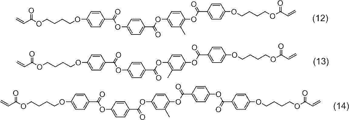
[In the compound (11), X 1 is 2 to 5 (integer)]
また、前述のように、広い帯域幅Δλ(選択反射を示す選択反射帯域の半値幅Δλ)および高い反射率を得るためには、コレステリック液晶相の屈折率異方性Δnが高い方が好ましい。従って、広い帯域幅Δλおよび高い反射率を得るためには、高い屈折率異方性Δnを示す重合性液晶化合物を用いるのが好ましい。具体的には、液晶組成物に用いる重合性液晶化合物の30℃における屈折率異方性Δnは、前述のように0.2以上が好ましく、0.25以上がより好ましく、0.3以上がさらに好ましく、0.35以上が特に好ましい。重合性液晶化合物の屈折率異方性Δnの上限は特に制限されないが、0.6以下の場合が多い。
屈折率異方性Δnの測定方法としては、液晶便覧(液晶便覧編集委員会編、丸善株式会社刊)202頁に記載の楔形液晶セルを用いた方法が一般的であり、結晶化しやすい化合物の場合は、他の液晶との混合物による評価を行い、その外挿値から見積もることもできる。 Further, as described above, in order to obtain a wide bandwidth Δλ (half-value width Δλ of the selective reflection band exhibiting selective reflection) and a high reflectance, it is preferable that the refractive index anisotropy Δn of the cholesteric liquid crystal phase is high. Therefore, in order to obtain a wide bandwidth Δλ and a high reflectance, it is preferable to use a polymerizable liquid crystal compound exhibiting a high refractive index anisotropy Δn. Specifically, the refractive index anisotropy Δn at 30 ° C. of the polymerizable liquid crystal compound used in the liquid crystal composition is preferably 0.2 or more, more preferably 0.25 or more, as described above, and 0.3 or more. Further preferred is 0.35 or more. The upper limit of the refractive index anisotropy Δn of the polymerizable liquid crystal compound is not particularly limited, but is often 0.6 or less.
As a method for measuring the refractive index anisotropy Δn, a method using a wedge-shaped liquid crystal cell described in page 202 of a liquid crystal handbook (edited by the Liquid Crystal Handbook Editorial Committee, published by Maruzen Co., Ltd.) is generally used. In this case, the evaluation can be performed by using a mixture with another liquid crystal and estimated from the extrapolated value.
高い屈折率異方性Δnを示す重合性液晶化合物としては、例えば、米国特許6514578号公報、特許3999400号公報、特許4117832号公報、特許4517416号公報、特許4836335号公報、特許5411770号公報、特許5411771号公報、特許5510321号公報、特許5705465号公報、特許5721484号公報、および、特許5723641号公報等に記載の化合物が挙げられる。
Examples of the polymerizable liquid crystal compound exhibiting a high refractive index anisotropy Δn include, for example, US Pat. Examples thereof include compounds described in Japanese Patent No. 5411717, Japanese Patent No. 5510321, Japanese Patent No. 5705465, Japanese Patent No. 5721484, and Japanese Patent No. 5723641.
重合性液晶化合物の他の好適な例としては、下記の一般式(1)で表される重合性液晶化合物が挙げられる。
Another preferred example of the polymerizable liquid crystal compound is a polymerizable liquid crystal compound represented by the following general formula (1).

一般式(1)において、A1~A4は、それぞれ独立に、置換基を有していてもよい芳香族炭素環または複素環を表す。芳香族炭素環としては、ベンゼン環およびナフタレン環が挙げられる。複素環としては、フラン環、チオフェン環、ピロール環、ピロリン環、ピロリジン環、オキサゾール環、イソオキサゾール環、チアゾール環、イソチアゾール環、イミダゾール環、イミダゾリン環、イミダゾリジン環、ピラゾール環、ピラゾリン環、ピラゾリジン環、トリアゾール環、フラザン環、テトラゾール環、ピラン環、チイン環、ピリジン環、ピペリジン環、オキサジン環、モルホリン環、チアジン環、ピリダジン環、ピリミジン環、ピラジン環、ピペラジン環、および、トリアジン環が挙げられる。なかでも、A1~A4は、芳香族炭素環であるのが好ましく、ベンゼン環であるのがより好ましい。
芳香族炭素環または複素環に置換してもよい置換基の種類は特に制限されず、例えば、ハロゲン原子、シアノ基、ニトロ基、アルキル基、ハロゲン置換アルキル基、アルコキシ基、アルキルチオ基、アシルオキシ基、アルコキシカルボニル基、カルバモイル基、アルキル置換カルバモイル基、および、炭素数が2~6のアシルアミノ基が挙げられる。 In the general formula (1), A 1 to A 4 each independently represents an aromatic carbocycle or heterocycle which may have a substituent. Examples of the aromatic carbocycle include a benzene ring and a naphthalene ring. As the heterocyclic ring, furan ring, thiophene ring, pyrrole ring, pyrroline ring, pyrrolidine ring, oxazole ring, isoxazole ring, thiazole ring, isothiazole ring, imidazole ring, imidazoline ring, imidazolidine ring, pyrazole ring, pyrazoline ring, Pyrazolidine ring, triazole ring, furazane ring, tetrazole ring, pyran ring, thiyne ring, pyridine ring, piperidine ring, oxazine ring, morpholine ring, thiazine ring, pyridazine ring, pyrimidine ring, pyrazine ring, piperazine ring, and triazine ring Can be mentioned. Among these, A 1 to A 4 are preferably aromatic carbocycles, and more preferably benzene rings.
The type of substituent that may be substituted on the aromatic carbocycle or heterocyclic ring is not particularly limited, and examples thereof include a halogen atom, a cyano group, a nitro group, an alkyl group, a halogen-substituted alkyl group, an alkoxy group, an alkylthio group, and an acyloxy group. , An alkoxycarbonyl group, a carbamoyl group, an alkyl-substituted carbamoyl group, and an acylamino group having 2 to 6 carbon atoms.
X1およびX2は、それぞれ独立に、単結合、-COO-、-OCO-、-CONH-、-NHCO-、-CH2CH2-、-OCH2-、-CH2O-、-CH=CH-、-CH=CH-COO-、-OCO-CH=CH-、または、-C≡C-を表す。なかでも、単結合、-COO-、-CONH-、-NHCO-、または、-C≡C-が好ましい。
Y1およびY2は、それぞれ独立に、単結合、-O-、-S-、-CO-、-COO-、-OCO-、-CONH-、-NHCO-、-CH=CH-、-CH=CH-COO-、-OCO-CH=CH-、または、-C≡C-を表す。なかでも、-O-が好ましい。
Sp1およびSp2は、それぞれ独立に、単結合、または、炭素数1~25の炭素鎖を表す。炭素鎖は、直鎖状、分岐鎖状、および、環状のいずれもよい。炭素鎖としては、いわゆるアルキル基が好ましい。なかでも、炭素数1~10のアルキル基がより好ましい。 X 1 and X 2 are each independently a single bond, —COO—, —OCO—, —CONH—, —NHCO—, —CH 2 CH 2 —, —OCH 2 —, —CH 2 O—, —CH ═CH—, —CH═CH—COO—, —OCO—CH═CH—, or —C≡C—. Of these, a single bond, —COO—, —CONH—, —NHCO—, or —C≡C— is preferable.
Y 1 and Y 2 are each independently a single bond, —O—, —S—, —CO—, —COO—, —OCO—, —CONH—, —NHCO—, —CH═CH—, —CH = CH-COO-, -OCO-CH = CH-, or -C≡C-. Of these, —O— is preferable.
Sp 1 and Sp 2 each independently represents a single bond or a carbon chain having 1 to 25 carbon atoms. The carbon chain may be linear, branched, or cyclic. As the carbon chain, a so-called alkyl group is preferable. Of these, an alkyl group having 1 to 10 carbon atoms is more preferable.
P1およびP2は、それぞれ独立に、水素原子または重合性基を表し、P1およびP2の少なくとも一方は重合性基を表す。重合性基としては、上述した重合性基を有する液晶化合物が有している重合性基が例示される。
n1およびn2はそれぞれ独立に0~2の整数を表し、n1またはn2が2の場合、複数あるA1、A2、X1およびX2は同じでもあっても異なっていてもよい。 P 1 and P 2 each independently represent a hydrogen atom or a polymerizable group, and at least one of P 1 and P 2 represents a polymerizable group. As a polymeric group, the polymeric group which the liquid crystal compound which has a polymeric group mentioned above has is illustrated.
n 1 and n 2 each independently represents an integer of 0 to 2, and when n 1 or n 2 is 2, a plurality of A 1 , A 2 , X 1 and X 2 may be the same or different. Good.
一般式(1)で表される重合性液晶化合物の具体例としては、下記式(1-1)~(1-30)に示す化合物が挙げられる。

Specific examples of the polymerizable liquid crystal compound represented by the general formula (1) include compounds represented by the following formulas (1-1) to (1-30).


また、上記以外の重合性液晶化合物としては、特開昭57-165480号公報に開示されているようなコレステリック相を有する環式オルガノポリシロキサン化合物等を用いることができる。さらに、前述の高分子液晶化合物としては、液晶を呈するメソゲン基を主鎖、側鎖、あるいは主鎖および側鎖の両方の位置に導入した高分子、コレステリル基を側鎖に導入した高分子コレステリック液晶、特開平9-133810号公報に開示されているような液晶性高分子、特開平11-293252号公報に開示されているような液晶性高分子等を用いることができる。
Further, as polymerizable liquid crystal compounds other than the above, cyclic organopolysiloxane compounds having a cholesteric phase as disclosed in JP-A-57-165480 can be used. Further, the above-mentioned polymer liquid crystal compound includes a polymer in which a mesogenic group exhibiting liquid crystal is introduced into the main chain, a side chain, or both positions of the main chain and the side chain, and a polymer cholesteric in which a cholesteryl group is introduced into the side chain. A liquid crystal, a liquid crystalline polymer as disclosed in JP-A-9-133810, a liquid crystalline polymer as disclosed in JP-A-11-293252, or the like can be used.
また、液晶組成物中の重合性液晶化合物の添加量は、液晶組成物の固形分質量(溶媒を除いた質量)に対して、75~99.9質量%であるのが好ましく、80~99質量%であるのがより好ましく、85~90質量%であるのがさらに好ましい。
The addition amount of the polymerizable liquid crystal compound in the liquid crystal composition is preferably 75 to 99.9% by mass with respect to the solid content mass (mass excluding the solvent) of the liquid crystal composition, and preferably 80 to 99. More preferably, it is more preferably 85% to 90% by weight.
--キラル剤(光学活性化合物)--
キラル剤はコレステリック液晶相の螺旋構造を誘起する機能を有する。キラル剤は、化合物によって誘起する螺旋の捩れ方向または螺旋ピッチが異なるため、目的に応じて選択すればよい。
すなわち、右円偏光コレステリック層16rを形成する際には、右捩れを誘起するキラル剤を用い、左円偏光コレステリック層16lを形成する際には、左捩れを誘起するキラル剤を用いればよい。 --Chiral agent (optically active compound)-
The chiral agent has a function of inducing a helical structure of a cholesteric liquid crystal phase. The chiral agent may be selected according to the purpose because the twist direction or the spiral pitch of the spiral induced by the compound is different.
That is, when the right circularly polarizedcholesteric layer 16r is formed, a chiral agent that induces right twist is used, and when the left circularly polarized cholesteric layer 16l is formed, a chiral agent that induces left twist is used.
キラル剤はコレステリック液晶相の螺旋構造を誘起する機能を有する。キラル剤は、化合物によって誘起する螺旋の捩れ方向または螺旋ピッチが異なるため、目的に応じて選択すればよい。
すなわち、右円偏光コレステリック層16rを形成する際には、右捩れを誘起するキラル剤を用い、左円偏光コレステリック層16lを形成する際には、左捩れを誘起するキラル剤を用いればよい。 --Chiral agent (optically active compound)-
The chiral agent has a function of inducing a helical structure of a cholesteric liquid crystal phase. The chiral agent may be selected according to the purpose because the twist direction or the spiral pitch of the spiral induced by the compound is different.
That is, when the right circularly polarized
キラル剤としては、特に制限はなく、公知の化合物(例えば、液晶デバイスハンドブック、第3章4-3項、TN(twisted nematic)、STN(Super Twisted Nematic)用カイラル剤、199頁、日本学術振興会第142委員会編、1989に記載)、イソソルビド、イソマンニド誘導体を用いることができる。
キラル剤は、一般に不斉炭素原子を含むが、不斉炭素原子を含まない軸性不斉化合物または面性不斉化合物もキラル剤として用いることができる。軸性不斉化合物または面性不斉化合物の例には、ビナフチル、ヘリセン、パラシクロファンおよびこれらの誘導体が含まれる。キラル剤は、重合性基を有していてもよい。キラル剤と液晶化合物とがいずれも重合性基を有する場合は、重合性キラル剤と重合性液晶化合物との重合反応により、重合性液晶化合物から誘導される繰り返し単位と、キラル剤から誘導される繰り返し単位とを有するポリマーを形成することができる。この態様では、重合性キラル剤が有する重合性基は、重合性液晶化合物が有する重合性基と、同種の基であるのが好ましい。従って、キラル剤の重合性基も、不飽和重合性基、エポキシ基またはアジリジニル基であるのが好ましく、不飽和重合性基であるのがより好ましく、エチレン性不飽和重合性基であるのがさらに好ましい。
また、キラル剤は、液晶化合物であってもよい。 The chiral agent is not particularly limited, and is a known compound (for example, liquid crystal device handbook, chapter 3-4-3, chiral agent for TN (twisted nematic), STN (Super Twisted Nematic), 199 pages, Japan Science Foundation) 142), 1989), isosorbide and isomannide derivatives can be used.
A chiral agent generally contains an asymmetric carbon atom, but an axially asymmetric compound or a planar asymmetric compound that does not contain an asymmetric carbon atom can also be used as the chiral agent. Examples of the axial asymmetric compound or the planar asymmetric compound include binaphthyl, helicene, paracyclophane, and derivatives thereof. The chiral agent may have a polymerizable group. When both the chiral agent and the liquid crystal compound have a polymerizable group, they are derived from the repeating unit derived from the polymerizable liquid crystal compound and the chiral agent by a polymerization reaction between the polymerizable chiral agent and the polymerizable liquid crystal compound. A polymer having repeating units can be formed. In this embodiment, the polymerizable group possessed by the polymerizable chiral agent is preferably the same group as the polymerizable group possessed by the polymerizable liquid crystal compound. Accordingly, the polymerizable group of the chiral agent is also preferably an unsaturated polymerizable group, an epoxy group or an aziridinyl group, more preferably an unsaturated polymerizable group, and an ethylenically unsaturated polymerizable group. Further preferred.
The chiral agent may be a liquid crystal compound.
キラル剤が光異性化基を有する場合には、塗布、配向後に活性光線などのフォトマスク照射によって、発光波長に対応した所望の反射波長のパターンを形成することができるので好ましい。光異性化基としては、フォトクロッミック性を示す化合物の異性化部位、アゾ基、アゾキシ基、シンナモイル基が好ましい。具体的な化合物として、特開2000-147236、特開2002-80478号公報、特開2002-80851号公報、特開2002-179633号公報、特開2002-179668号公報、特開2002-179669号公報、特開2002-179670号公報、特開2002-179681号公報、特開2002-179682号公報、特開2002-302487号公報、特開2002-338575号公報、特開2002-338668号公報、特開2003-306490号公報、特開2003-306491号公報、特開2003-313187号公報、特開2003-313188号公報、特開2003-313189号公報、および、特開2003-313292号公報に記載の化合物を用いることができる。
It is preferable that the chiral agent has a photoisomerizable group because a pattern having a desired reflection wavelength corresponding to the emission wavelength can be formed by photomask irradiation such as actinic rays after coating and orientation. As the photoisomerization group, an isomerization site of a compound exhibiting photochromic properties, an azo group, an azoxy group, or a cinnamoyl group is preferable. As specific compounds, JP-A 2000-147236, JP-A 2002-80478, JP-A 2002-80851, JP-A 2002-179633, JP-A 2002-179668, JP-A 2002-179669. JP, JP-A-2002-179670, JP-A-2002-179681, JP-A-2002-179682, JP-A-2002-302487, JP-A-2002-338575, JP-A-2002-338668, JP-A-2003-306490, JP-A-2003-306491, JP-A-2003-313187, JP-A-2003-313188, JP-A-2003-313189, and JP-A-2003-313292 The described compounds can be used.
液晶組成物における、キラル剤の含有量は、重合性液晶化合物量の0.01~200モル%が好ましく、1~30モル%がより好ましい。
The content of the chiral agent in the liquid crystal composition is preferably 0.01 to 200 mol%, more preferably 1 to 30 mol%, based on the amount of the polymerizable liquid crystal compound.
--重合開始剤--
液晶組成物が重合性化合物を含む場合は、重合開始剤を含有しているのが好ましい。紫外線照射により重合反応を進行させる態様では、使用する重合開始剤は、紫外線照射によって重合反応を開始可能な光重合開始剤であるのが好ましい。光重合開始剤の例には、α-カルボニル化合物(米国特許第2367661号、同2367670号の各明細書記載)、アシロインエーテル(米国特許第2448828号明細書記載)、α-炭化水素置換芳香族アシロイン化合物(米国特許第2722512号明細書記載)、多核キノン化合物(米国特許第3046127号および同2951758号の各明細書記載)、トリアリールイミダゾールダイマーとp-アミノフェニルケトンとの組み合わせ(米国特許第3549367号明細書記載)、アクリジンおよびフェナジン化合物(特開昭60-105667号公報および米国特許第4239850号明細書記載)および、オキサジアゾール化合物(米国特許第4212970号明細書記載)等が挙げられる。
液晶組成物中の光重合開始剤の含有量は、重合性液晶化合物の含有量に対して0.1~20質量%であるのが好ましく、0.5~12質量%であるのがさらに好ましい。 --Polymerization initiator--
When the liquid crystal composition contains a polymerizable compound, it preferably contains a polymerization initiator. In the embodiment in which the polymerization reaction is advanced by ultraviolet irradiation, the polymerization initiator to be used is preferably a photopolymerization initiator that can start the polymerization reaction by ultraviolet irradiation. Examples of photopolymerization initiators include α-carbonyl compounds (described in US Pat. Nos. 2,367,661 and 2,367,670), acyloin ether (described in US Pat. No. 2,448,828), α-hydrocarbon substituted aromatics. Group acyloin compounds (described in US Pat. No. 2,722,512), polynuclear quinone compounds (described in US Pat. Nos. 3,046,127 and 2,951,758), a combination of triarylimidazole dimer and p-aminophenyl ketone (US patent) No. 3549367), acridine and phenazine compounds (described in JP-A-60-105667 and US Pat. No. 4,239,850), oxadiazole compounds (described in US Pat. No. 4,221,970) and the like It is done.
The content of the photopolymerization initiator in the liquid crystal composition is preferably 0.1 to 20% by mass, more preferably 0.5 to 12% by mass with respect to the content of the polymerizable liquid crystal compound. .
--架橋剤--
液晶組成物は、硬化後の膜強度向上、耐久性向上のため、任意に架橋剤を含有していてもよい。架橋剤としては、紫外線、熱、湿気等で硬化するものが好適に使用できる。
架橋剤としては、特に制限はなく、目的に応じて適宜選択することができ、例えばトリメチロールプロパントリ(メタ)アクリレート、ペンタエリスリトールトリ(メタ)アクリレート等の多官能アクリレート化合物;グリシジル(メタ)アクリレート、エチレングリコールジグリシジルエーテル等のエポキシ化合物;2,2-ビスヒドロキシメチルブタノール-トリス[3-(1-アジリジニル)プロピオネート]、4,4-ビス(エチレンイミノカルボニルアミノ)ジフェニルメタン等のアジリジン化合物;ヘキサメチレンジイソシアネート、ビウレット型イソシアネート等のイソシアネート化合物;オキサゾリン基を側鎖に有するポリオキサゾリン化合物;および、ビニルトリメトキシシラン、N-(2-アミノエチル)3-アミノプロピルトリメトキシシラン等のアルコキシシラン化合物などが挙げられる。また、架橋剤の反応性に応じて公知の触媒を用いるのができ、膜強度および耐久性向上に加えて生産性を向上させることができる。これらは、1種を単独で使用してもよいし、2種以上を併用してもよい。
架橋剤の含有量は、液晶組成物の固形分質量に対して、3~20質量%が好ましく、5~15質量%がより好ましい。架橋剤の含有量が上記範囲内であれば、架橋密度向上の効果が得られやすく、コレステリック液晶相の安定性がより向上する。 -Crosslinking agent-
The liquid crystal composition may optionally contain a crosslinking agent in order to improve the film strength after curing and improve the durability. As the cross-linking agent, one that can be cured by ultraviolet rays, heat, moisture, or the like can be suitably used.
There is no restriction | limiting in particular as a crosslinking agent, According to the objective, it can select suitably, For example, polyfunctional acrylate compounds, such as a trimethylol propane tri (meth) acrylate and pentaerythritol tri (meth) acrylate; Glycidyl (meth) acrylate , Epoxy compounds such as ethylene glycol diglycidyl ether; aziridine compounds such as 2,2-bishydroxymethylbutanol-tris [3- (1-aziridinyl) propionate], 4,4-bis (ethyleneiminocarbonylamino) diphenylmethane; hexa Isocyanate compounds such as methylene diisocyanate and biuret type isocyanate; polyoxazoline compounds having an oxazoline group in the side chain; and vinyltrimethoxysilane, N- (2-aminoethyl) 3-amino Alkoxysilane compounds such as pills trimethoxysilane. Further, a known catalyst can be used according to the reactivity of the crosslinking agent, and productivity can be improved in addition to improvement in film strength and durability. These may be used individually by 1 type and may use 2 or more types together.
The content of the crosslinking agent is preferably 3 to 20% by mass and more preferably 5 to 15% by mass with respect to the solid content mass of the liquid crystal composition. If content of a crosslinking agent is in the said range, the effect of a crosslinking density improvement will be easy to be acquired, and stability of a cholesteric liquid crystal phase will improve more.
--重合禁止剤--
液晶組成物は、保存性の向上を目的として、重合禁止剤を含有してもよい。
重合禁止剤としては、例えば、ハイドロキノン、ハイドロキノンモノメチルエーテル、フェノチアジン、ベンゾキノン、ヒンダードアミン(HALS)、および、これらの誘導体等が挙げられる。これらは、1種を単独で使用してもよいし、2種以上を併用してもよい。
重合禁止剤の含有量は、液晶組成物の固形分質量に対して、0~10質量%が好ましく、0~5質量%がより好ましい。 --- Polymerization inhibitor--
The liquid crystal composition may contain a polymerization inhibitor for the purpose of improving storage stability.
Examples of the polymerization inhibitor include hydroquinone, hydroquinone monomethyl ether, phenothiazine, benzoquinone, hindered amine (HALS), and derivatives thereof. These may be used individually by 1 type and may use 2 or more types together.
The content of the polymerization inhibitor is preferably 0 to 10% by mass and more preferably 0 to 5% by mass with respect to the mass of the solid content of the liquid crystal composition.
液晶組成物は、コレステリック液晶層を形成する際には、液体として用いられるのが好ましい。
液晶組成物は溶媒を含んでいてもよい。溶媒としては、特に制限はなく、目的に応じて適宜選択することができるが、有機溶媒が好ましく用いられる。
有機溶媒としては、特に制限はなく、目的に応じて適宜選択することができ、例えば、メチルエチルケトン、メチルイソブチルケトン、シクロヘキサノンおよびシクロペンタノン等のケトン類、アルキルハライド類、アミド類、スルホキシド類、ヘテロ環化合物、炭化水素類、エステル類、および、エーテル類などが挙げられる。これらは、1種を単独で使用してもよいし、2種以上を併用してもよい。これらの中でも、環境への負荷を考慮した場合にはケトン類が好ましい。上述の単官能重合性モノマーなどの上述の成分が溶媒として機能していてもよい。 The liquid crystal composition is preferably used as a liquid when forming a cholesteric liquid crystal layer.
The liquid crystal composition may contain a solvent. There is no restriction | limiting in particular as a solvent, Although it can select suitably according to the objective, An organic solvent is used preferably.
The organic solvent is not particularly limited and may be appropriately selected depending on the intended purpose. For example, ketones such as methyl ethyl ketone, methyl isobutyl ketone, cyclohexanone and cyclopentanone, alkyl halides, amides, sulfoxides, hetero Examples thereof include ring compounds, hydrocarbons, esters, and ethers. These may be used individually by 1 type and may use 2 or more types together. Among these, ketones are preferable in consideration of environmental load. The above-described components such as the above-mentioned monofunctional polymerizable monomer may function as a solvent.
右円偏光コレステリック層16rは、一例として、右捩れを誘起するキラル剤を含む右円偏光コレステリック層16rを形成するための液晶組成物を、吸収型カラーフィルター14の上に塗布する工程、加熱によって右円偏光反射特性を有するコレステリック液晶相とする工程、および、紫外線の照射(紫外線の露光)によってコレステリック液晶相を固定化する工程を行って、形成すればよい。
他方、左円偏光コレステリック層16lは、一例として、左捩れを誘起するキラル剤を含む左円偏光コレステリック層16lを形成するための液晶組成物を、先に形成した右円偏光コレステリック層16rの上に塗布する工程、加熱によって右円偏光反射特性を有するコレステリック液晶相とする工程、および、紫外線の照射(紫外線の露光)によってコレステリック液晶相を固定化する工程を行って、形成すればよい。
なお、液晶組成物の塗布、乾燥、および、紫外線の照射は、いずれも、公知の方法で行えばよい。 As an example, the right circularly polarizedcholesteric layer 16r is formed by applying a liquid crystal composition for forming the right circularly polarized cholesteric layer 16r containing a chiral agent that induces right twist on the absorption color filter 14, by heating. What is necessary is just to form by performing the process which makes a cholesteric liquid crystal phase which has a right circular polarization reflective characteristic, and the process which fixes a cholesteric liquid crystal phase by ultraviolet irradiation (exposure of ultraviolet light).
On the other hand, the left circularly polarized cholesteric layer 16l is, for example, a liquid crystal composition for forming the left circularly polarized cholesteric layer 16l containing a chiral agent that induces left twist is formed on the right circularly polarizedcholesteric layer 16r. It may be formed by performing a step of coating on the surface, a step of forming a cholesteric liquid crystal phase having right circular polarization reflection characteristics by heating, and a step of fixing the cholesteric liquid crystal phase by irradiation with ultraviolet rays (ultraviolet exposure).
Note that the application, drying, and ultraviolet irradiation of the liquid crystal composition may all be performed by known methods.
他方、左円偏光コレステリック層16lは、一例として、左捩れを誘起するキラル剤を含む左円偏光コレステリック層16lを形成するための液晶組成物を、先に形成した右円偏光コレステリック層16rの上に塗布する工程、加熱によって右円偏光反射特性を有するコレステリック液晶相とする工程、および、紫外線の照射(紫外線の露光)によってコレステリック液晶相を固定化する工程を行って、形成すればよい。
なお、液晶組成物の塗布、乾燥、および、紫外線の照射は、いずれも、公知の方法で行えばよい。 As an example, the right circularly polarized
On the other hand, the left circularly polarized cholesteric layer 16l is, for example, a liquid crystal composition for forming the left circularly polarized cholesteric layer 16l containing a chiral agent that induces left twist is formed on the right circularly polarized
Note that the application, drying, and ultraviolet irradiation of the liquid crystal composition may all be performed by known methods.
ここで、前述のように、キラル剤としては、シンナモイル基などの光で異性化する部分(光異性化基)を有するキラル剤が利用可能である。液晶組成物のキラル剤として、光異性化基を有するキラル剤を用いた場合には、液晶組成物を塗布して加熱を行った後、弱い紫外線をパターニングして照射することを1回以上行って、光異性化基を異性化し、その後、コレステリック液晶相を固定化するための紫外線の照射を行ってもよい。
あるいは、コレステリック液晶相を固定化するための強い紫外線をパターニングして照射することで部分的に硬化させた後に、未露光部もしくは全面に弱い紫外線を照射することで光異性化基を異性化し、その後、コレステリック液晶相を固定化するための紫外線の照射を行ってもよい。
これにより、右円偏光コレステリック層16rおよび左円偏光コレステリック層16lが、面内に、異なる波長領域の光を反射する反射領域を、複数、有する構成にできる。なお、この場合には、右円偏光コレステリック層16rおよび左円偏光コレステリック層16lは、互いの同じ波長領域の光を反射する反射領域を、面方向に同じ位置に積層するのが好ましい。 Here, as described above, as the chiral agent, a chiral agent having a moiety (photoisomerization group) that isomerizes with light, such as a cinnamoyl group, can be used. When a chiral agent having a photoisomerizable group is used as a chiral agent of the liquid crystal composition, after applying the liquid crystal composition and heating, patterning with weak ultraviolet rays is performed at least once. Then, the photoisomerization group may be isomerized and then irradiated with ultraviolet rays for fixing the cholesteric liquid crystal phase.
Alternatively, after partially curing by patterning and irradiating strong ultraviolet rays for fixing the cholesteric liquid crystal phase, the photoisomerization group is isomerized by irradiating weak UV rays to the unexposed areas or the entire surface, Thereafter, irradiation with ultraviolet rays for fixing the cholesteric liquid crystal phase may be performed.
As a result, the right circularly polarizedcholesteric layer 16r and the left circularly polarized cholesteric layer 16l can have a plurality of reflective regions that reflect light in different wavelength regions in the plane. In this case, it is preferable that the right circularly polarized cholesteric layer 16r and the left circularly polarized cholesteric layer 16l are formed by stacking reflection regions that reflect light in the same wavelength region in the same position in the plane direction.
あるいは、コレステリック液晶相を固定化するための強い紫外線をパターニングして照射することで部分的に硬化させた後に、未露光部もしくは全面に弱い紫外線を照射することで光異性化基を異性化し、その後、コレステリック液晶相を固定化するための紫外線の照射を行ってもよい。
これにより、右円偏光コレステリック層16rおよび左円偏光コレステリック層16lが、面内に、異なる波長領域の光を反射する反射領域を、複数、有する構成にできる。なお、この場合には、右円偏光コレステリック層16rおよび左円偏光コレステリック層16lは、互いの同じ波長領域の光を反射する反射領域を、面方向に同じ位置に積層するのが好ましい。 Here, as described above, as the chiral agent, a chiral agent having a moiety (photoisomerization group) that isomerizes with light, such as a cinnamoyl group, can be used. When a chiral agent having a photoisomerizable group is used as a chiral agent of the liquid crystal composition, after applying the liquid crystal composition and heating, patterning with weak ultraviolet rays is performed at least once. Then, the photoisomerization group may be isomerized and then irradiated with ultraviolet rays for fixing the cholesteric liquid crystal phase.
Alternatively, after partially curing by patterning and irradiating strong ultraviolet rays for fixing the cholesteric liquid crystal phase, the photoisomerization group is isomerized by irradiating weak UV rays to the unexposed areas or the entire surface, Thereafter, irradiation with ultraviolet rays for fixing the cholesteric liquid crystal phase may be performed.
As a result, the right circularly polarized
また、紫外線照射時の温度を調節することで、反射波長領域を調節することも可能である。温度を調節しながら、紫外線をパターニングして照射することで、右円偏光コレステリック層16rおよび左円偏光コレステリック層16lが、面内に、異なる波長領域の光を反射する反射領域を、複数、有する構成にできる。特に、液晶組成物の等方相温度以上に加熱した状態で、紫外線照射をすることで、いずれの波長領域にも反射特性を持たない透過領域を面内に形成することができる。
Also, the reflection wavelength region can be adjusted by adjusting the temperature at the time of ultraviolet irradiation. The right circularly polarized cholesteric layer 16r and the left circularly polarized cholesteric layer 16l have a plurality of reflective regions that reflect light of different wavelength regions in the plane by patterning and irradiating ultraviolet rays while adjusting the temperature. Can be configured. In particular, by irradiating with ultraviolet rays in a state where the liquid crystal composition is heated to an isotropic phase temperature or higher, a transmission region having no reflection characteristics in any wavelength region can be formed in the plane.
以下、イメージセンサー10の作用について説明する。なお、以下の説明では、一例として、コレステリック反射層16が780nm超1200nm以下の波長範囲の近赤外線を反射(遮断)するものとする。
イメージセンサー10に光が入射すると、まず、左円偏光コレステリック層16lによって780nm超1200nm以下の波長領域の近赤外線の左円偏光が反射され、それ以外の光は透過して、右円偏光コレステリック層16rに入射する。
右円偏光コレステリック層16rに光が入射すると、780nm超1200nm以下の波長領域の近赤外線の右円偏光が反射され、それ以外の光は透過する。従って、これにより、780nm超1200nm以下の波長領域の近赤外線は、全て遮断される。
右円偏光コレステリック層16rを透過した光は、吸収型カラーフィルター14の赤色フィルター14R、緑色フィルター14Gおよび青色フィルター14Bのいずれかによって、赤色光、緑色光あるいは青色光とされ、固体撮像素子12aによって測光され、画像データとして出力される。 Hereinafter, the operation of theimage sensor 10 will be described. In the following description, as an example, it is assumed that the cholesteric reflective layer 16 reflects (blocks) near infrared rays in a wavelength range of more than 780 nm and not more than 1200 nm.
When light is incident on theimage sensor 10, first, the left circularly polarized cholesteric layer 16l reflects near-infrared left circularly polarized light in a wavelength region of more than 780 nm and not more than 1200 nm, and other light is transmitted to the right circularly polarized cholesteric layer. It is incident on 16r.
When light is incident on the right circularly polarizedcholesteric layer 16r, near-infrared right circularly polarized light in a wavelength region of more than 780 nm and not more than 1200 nm is reflected, and other light is transmitted. Therefore, all near infrared rays in the wavelength region of more than 780 nm and not more than 1200 nm are blocked by this.
The light transmitted through the right circularly polarizedcholesteric layer 16r is converted into red light, green light, or blue light by any one of the red filter 14R, the green filter 14G, and the blue filter 14B of the absorption color filter 14, and is transmitted by the solid-state imaging device 12a. The light is measured and output as image data.
イメージセンサー10に光が入射すると、まず、左円偏光コレステリック層16lによって780nm超1200nm以下の波長領域の近赤外線の左円偏光が反射され、それ以外の光は透過して、右円偏光コレステリック層16rに入射する。
右円偏光コレステリック層16rに光が入射すると、780nm超1200nm以下の波長領域の近赤外線の右円偏光が反射され、それ以外の光は透過する。従って、これにより、780nm超1200nm以下の波長領域の近赤外線は、全て遮断される。
右円偏光コレステリック層16rを透過した光は、吸収型カラーフィルター14の赤色フィルター14R、緑色フィルター14Gおよび青色フィルター14Bのいずれかによって、赤色光、緑色光あるいは青色光とされ、固体撮像素子12aによって測光され、画像データとして出力される。 Hereinafter, the operation of the
When light is incident on the
When light is incident on the right circularly polarized
The light transmitted through the right circularly polarized
以上のように、本発明のイメージセンサー10によれば、一例として、固体撮像素子12aが感度を有する780nm超1200nm以下の波長領域の近赤外線を除去して、赤色光、緑色光および青色光を測光できるので、赤外線に起因するノイズが少ない、適正な画像データを出力できる。
また、従来はイメージセンサーとは離間して別体として設けられていた赤外線を遮断(カット)する赤外線フィルターを、コレステリック反射層16としてイメージセンサー10に積層あるいは組み込むことができるので、イメージセンサー10を利用する撮像装置(撮像モジュール)の高さ(厚さ)を大幅に削減できる。
しかも、赤外線フィルターであるコレステリック反射層16は、液晶組成物を用いる塗布法で形成できるので、多層膜赤外反射層のように無機層の蒸着では困難であった、粒状等の欠陥の無い赤外線フィルターを形成でき、欠陥に起因する画質低下も防止できる。 As described above, according to theimage sensor 10 of the present invention, as an example, the near-infrared ray in the wavelength region of more than 780 nm and less than or equal to 1200 nm that the solid-state imaging device 12a has sensitivity is removed, and red light, green light, and blue light are emitted. Since photometry is possible, it is possible to output appropriate image data with less noise caused by infrared rays.
In addition, an infrared filter that cuts off (cuts) infrared rays, which has been provided separately from the image sensor in the past, can be stacked or incorporated in theimage sensor 10 as the cholesteric reflection layer 16. The height (thickness) of the imaging device (imaging module) to be used can be greatly reduced.
In addition, since the cholestericreflective layer 16 that is an infrared filter can be formed by a coating method using a liquid crystal composition, it is difficult to deposit inorganic layers, such as multilayer infrared reflective layers, and has no defects such as granularity. A filter can be formed and image quality deterioration due to defects can be prevented.
また、従来はイメージセンサーとは離間して別体として設けられていた赤外線を遮断(カット)する赤外線フィルターを、コレステリック反射層16としてイメージセンサー10に積層あるいは組み込むことができるので、イメージセンサー10を利用する撮像装置(撮像モジュール)の高さ(厚さ)を大幅に削減できる。
しかも、赤外線フィルターであるコレステリック反射層16は、液晶組成物を用いる塗布法で形成できるので、多層膜赤外反射層のように無機層の蒸着では困難であった、粒状等の欠陥の無い赤外線フィルターを形成でき、欠陥に起因する画質低下も防止できる。 As described above, according to the
In addition, an infrared filter that cuts off (cuts) infrared rays, which has been provided separately from the image sensor in the past, can be stacked or incorporated in the
In addition, since the cholesteric
図2に、本発明のカラーフィルターの別の例を用いる本発明のイメージセンサーの別の例を概念的に示す。
図2に示すイメージセンサー20は、センサー本体12と、吸収型カラーフィルター14と、マイクロレンズ24と、平坦化層26と、コレステリック反射層16とを有して構成される。コレステリック反射層16は、右円偏光コレステリック層16rと左円偏光コレステリック層16lと有して構成される。図2に示す例において、本発明のカラーフィルターは、吸収型カラーフィルター14と、マイクロレンズ24と、平坦化層26と、コレステリック反射層16とで構成される。 FIG. 2 conceptually shows another example of the image sensor of the present invention using another example of the color filter of the present invention.
Animage sensor 20 shown in FIG. 2 includes a sensor body 12, an absorption color filter 14, a microlens 24, a planarization layer 26, and a cholesteric reflection layer 16. The cholesteric reflective layer 16 includes a right circularly polarized cholesteric layer 16r and a left circularly polarized cholesteric layer 16l. In the example shown in FIG. 2, the color filter of the present invention includes an absorption color filter 14, a microlens 24, a planarization layer 26, and a cholesteric reflection layer 16.
図2に示すイメージセンサー20は、センサー本体12と、吸収型カラーフィルター14と、マイクロレンズ24と、平坦化層26と、コレステリック反射層16とを有して構成される。コレステリック反射層16は、右円偏光コレステリック層16rと左円偏光コレステリック層16lと有して構成される。図2に示す例において、本発明のカラーフィルターは、吸収型カラーフィルター14と、マイクロレンズ24と、平坦化層26と、コレステリック反射層16とで構成される。 FIG. 2 conceptually shows another example of the image sensor of the present invention using another example of the color filter of the present invention.
An
図2に示すイメージセンサー20は、吸収型カラーフィルター14とコレステリック反射層16との間に、マイクロレンズ24および平坦化層26を有する以外は、図1に示すイメージセンサー10と同じ構成を有するので、同じ部材には同じ符号を付し、以下の説明は、異なる部位を主に行う。
The image sensor 20 shown in FIG. 2 has the same configuration as the image sensor 10 shown in FIG. 1 except that the microlens 24 and the flattening layer 26 are provided between the absorption color filter 14 and the cholesteric reflective layer 16. The same reference numerals are given to the same members, and the following description mainly focuses on different parts.
図2に示すイメージセンサー20は、吸収型カラーフィルター14の赤色フィルター14R、緑色フィルター14Gおよび青色フィルター14Bの個々に対応して、すなわち、固体撮像素子12aの個々に対応して、マイクロレンズ24が設けられる。
マイクロレンズ24は、中心が縁よりも厚く形成された凸型レンズであり、固体撮像素子12aに光を集光させるものである。各マイクロレンズ28は、全て同一形状である。 In theimage sensor 20 shown in FIG. 2, the microlens 24 corresponds to each of the red filter 14R, the green filter 14G, and the blue filter 14B of the absorption color filter 14, that is, corresponding to each of the solid-state imaging device 12a. Provided.
Themicro lens 24 is a convex lens whose center is formed thicker than the edge, and condenses light on the solid-state imaging device 12a. All the microlenses 28 have the same shape.
マイクロレンズ24は、中心が縁よりも厚く形成された凸型レンズであり、固体撮像素子12aに光を集光させるものである。各マイクロレンズ28は、全て同一形状である。 In the
The
このようなマイクロレンズ24は、レンズとして必要な光学特性を満たすものであれば公知の各種の材料で形成できる。マイクロレンズ24は、一例として、樹脂材料によって形成されるが、これに制限はされない。マイクロレンズ24に利用される樹脂材料としては、例えば、スチレン系樹脂、(メタ)アクリル系樹脂、スチレン-アクリル共重合系樹脂、および、シロキサン系樹脂等が例示される。
Such a microlens 24 can be formed of various known materials as long as they satisfy optical characteristics necessary for the lens. The microlens 24 is formed of a resin material as an example, but is not limited thereto. Examples of the resin material used for the microlens 24 include styrene resin, (meth) acrylic resin, styrene-acrylic copolymer resin, and siloxane resin.
平坦化層26は、凸レンズであるマイクロレンズ24の上のコレステリック反射層16側の表面を平坦化するものである。なお、平坦化層26は、上層と貼り合わせるための貼合層(接着層)を兼ねてもよい。図示例では、平坦化層26の上層は、コレステリック反射層16であり、具体的には、右円偏光コレステリック層16rである。
平坦化層26は、十分な光透過性を有するものであればよく、例えば、各種の樹脂材料で形成される。平坦化層26を形成する樹脂材料としては、一例として、フッ素含有シロキサン樹脂などのフッ素含有シラン化合物、(メタ)アクリル系樹脂、スチレン系樹脂、および、エポキシ系樹脂等が例示される。 Theflattening layer 26 flattens the surface on the cholesteric reflective layer 16 side on the microlens 24 that is a convex lens. The planarizing layer 26 may also serve as a bonding layer (adhesive layer) for bonding to the upper layer. In the illustrated example, the upper layer of the planarizing layer 26 is the cholesteric reflective layer 16, specifically, the right circularly polarized cholesteric layer 16 r.
Theflattening layer 26 only needs to have sufficient light transmittance, and is formed of, for example, various resin materials. Examples of the resin material for forming the planarizing layer 26 include fluorine-containing silane compounds such as fluorine-containing siloxane resins, (meth) acrylic resins, styrene resins, and epoxy resins.
平坦化層26は、十分な光透過性を有するものであればよく、例えば、各種の樹脂材料で形成される。平坦化層26を形成する樹脂材料としては、一例として、フッ素含有シロキサン樹脂などのフッ素含有シラン化合物、(メタ)アクリル系樹脂、スチレン系樹脂、および、エポキシ系樹脂等が例示される。 The
The
なお、マイクロレンズ24と平坦化層26とは、マイクロレンズ24の屈折率が平坦化層の屈折率よりも大きいのが好ましい。
また、平坦化層26を設けるのではなく、コレステリック反射層16をマイクロレンズ24とは離間して支持する支持手段を設けて、マイクロレンズ24とコレステリック反射層16との間に空気層を設けることにより、この空気層を、マイクロレンズ24の上を平坦化する平坦化層26として作用させてもよい。 Note that themicrolens 24 and the planarization layer 26 preferably have a refractive index of the microlens 24 larger than that of the planarization layer.
Further, instead of providing theplanarizing layer 26, a support means for supporting the cholesteric reflective layer 16 separately from the microlens 24 is provided, and an air layer is provided between the microlens 24 and the cholesteric reflective layer 16. Thus, this air layer may act as a flattening layer 26 for flattening the microlens 24.
また、平坦化層26を設けるのではなく、コレステリック反射層16をマイクロレンズ24とは離間して支持する支持手段を設けて、マイクロレンズ24とコレステリック反射層16との間に空気層を設けることにより、この空気層を、マイクロレンズ24の上を平坦化する平坦化層26として作用させてもよい。 Note that the
Further, instead of providing the
図2に示すイメージセンサー20のように、吸収型カラーフィルター14とコレステリック反射層16との間に、何らかの層を有する場合には、吸収型カラーフィルター14とコレステリック反射層16との間隔を100μm以下とするのが好ましい。なお、吸収型カラーフィルター14とコレステリック反射層16との間の何らかの層としては、空気層も例示される。
これにより、内部反射等に起因して、吸収型カラーフィルター14の各色のフィルターを透過した光が、直下ではなく隣接する固体撮像素子12aに入射する迷光(ゴースト)の発生を抑えることができる。 When there is some layer between theabsorption color filter 14 and the cholesteric reflection layer 16 as in the image sensor 20 shown in FIG. 2, the distance between the absorption color filter 14 and the cholesteric reflection layer 16 is 100 μm or less. Is preferable. An air layer is also exemplified as any layer between the absorption color filter 14 and the cholesteric reflective layer 16.
Thereby, it is possible to suppress the generation of stray light (ghost), which is caused by internal reflection or the like, and is transmitted through the filters of the respective colors of theabsorption color filter 14 and enters the adjacent solid-state imaging device 12a instead of immediately below.
これにより、内部反射等に起因して、吸収型カラーフィルター14の各色のフィルターを透過した光が、直下ではなく隣接する固体撮像素子12aに入射する迷光(ゴースト)の発生を抑えることができる。 When there is some layer between the
Thereby, it is possible to suppress the generation of stray light (ghost), which is caused by internal reflection or the like, and is transmitted through the filters of the respective colors of the
図2に示すイメージセンサー20は、前述のイメージセンサー10の製造において、吸収型カラーフィルター14の形成(フィルター形成工程)と、コレステリック反射層16の形成(コレステリック反射層形成工程)との間に、吸収型カラーフィルター14の上にマイクロレンズ24を形成する工程(マイクロレンズ形成工程)と、その後のマイクロレンズ24を覆って平坦化層26を形成する工程(平坦化層形成工程)を行うことで、作製できる。
なお、マイクロレンズ24は、形成材料に応じた公知の方法で形成すればよい。また、平坦化層26も、形成材料に応じた公知の方法で形成すればよい。 Theimage sensor 20 shown in FIG. 2 is formed between the formation of the absorption color filter 14 (filter formation process) and the formation of the cholesteric reflection layer 16 (cholesteric reflection layer formation process) in the manufacture of the image sensor 10 described above. By performing the step of forming the microlens 24 on the absorption color filter 14 (microlens formation step) and the step of forming the flattening layer 26 so as to cover the microlens 24 (planarization layer forming step). Can be produced.
Themicrolens 24 may be formed by a known method corresponding to the forming material. Further, the planarization layer 26 may be formed by a known method corresponding to the forming material.
なお、マイクロレンズ24は、形成材料に応じた公知の方法で形成すればよい。また、平坦化層26も、形成材料に応じた公知の方法で形成すればよい。 The
The
図3に、本発明のカラーフィルターの別の例を用いる本発明のイメージセンサーの別の例を概念的に示す。
図3に示すイメージセンサー30は、センサー本体12と、吸収型カラーフィルター14と、マイクロレンズ24と、平坦化層26と、コレステリック配向層32と、コレステリック反射層16(右円偏光コレステリック層16rおよび左円偏光コレステリック層16l)と、赤外吸収層34と、反射防止層36とを有して構成される。図3に示す例において、本発明のカラーフィルターは、吸収型カラーフィルター14と、マイクロレンズ24と、平坦化層26と、コレステリック配向層32と、コレステリック反射層16と、赤外吸収層34と、反射防止層36とで構成される。 FIG. 3 conceptually shows another example of the image sensor of the present invention using another example of the color filter of the present invention.
Theimage sensor 30 shown in FIG. 3 includes a sensor body 12, an absorption color filter 14, a microlens 24, a planarization layer 26, a cholesteric alignment layer 32, a cholesteric reflection layer 16 (right circularly polarized cholesteric layer 16r and The left circularly polarized cholesteric layer 16l), the infrared absorption layer 34, and the antireflection layer 36 are included. In the example shown in FIG. 3, the color filter of the present invention includes an absorption color filter 14, a microlens 24, a planarization layer 26, a cholesteric alignment layer 32, a cholesteric reflection layer 16, and an infrared absorption layer 34. And the antireflection layer 36.
図3に示すイメージセンサー30は、センサー本体12と、吸収型カラーフィルター14と、マイクロレンズ24と、平坦化層26と、コレステリック配向層32と、コレステリック反射層16(右円偏光コレステリック層16rおよび左円偏光コレステリック層16l)と、赤外吸収層34と、反射防止層36とを有して構成される。図3に示す例において、本発明のカラーフィルターは、吸収型カラーフィルター14と、マイクロレンズ24と、平坦化層26と、コレステリック配向層32と、コレステリック反射層16と、赤外吸収層34と、反射防止層36とで構成される。 FIG. 3 conceptually shows another example of the image sensor of the present invention using another example of the color filter of the present invention.
The
図3に示すイメージセンサー30は、コレステリック配向層32と、赤外吸収層34と、反射防止層36とを有する以外は、図2に示すイメージセンサー20と同じ構成を有するので、同じ部材には同じ符号を付し、以下の説明は、異なる部位を主に行う。
The image sensor 30 shown in FIG. 3 has the same configuration as the image sensor 20 shown in FIG. 2 except that it has a cholesteric alignment layer 32, an infrared absorption layer 34, and an antireflection layer 36. The same reference numerals are given, and the following description mainly focuses on different parts.
コレステリック配向層32は、右円偏光コレステリック層16rおよび左円偏光コレステリック層16lにおけるコレステリック液晶相の配向を保持するための層である。
コレステリック配向層32は、コレステリック液晶層の配向膜として用いられている公知の物が、各種、利用可能である。
好ましくは、コレステリック配向層32は、光配向膜である。光配向膜とは、一例として、アゾベンゼン系ポリマーおよびポリビニルシンナメート等の光活性分子に光化学反応を起こす波長の直線偏光や斜め非偏光を照射して光配向膜の表面に異方性を生成させるものであり、入射光によって膜の最表面の分子長軸の配向が生成され、この最表面の分子に接触する液晶を配向させる配向規制力が形成されている。
なお、光配向膜の材料としては、上述のものの他に、光活性分子が光化学反応を起こす波長の直線偏光照射による光異性化、光二量化、光環化、光架橋、光分解、および、光分解-結合のうち、いずれかの反応により膜表面に異方性を生成するものであればよく、例えば、「長谷川雅樹、日本液晶学会誌、Vol.3 No.1,p3(1999)」、「竹内安正、日本液晶学会誌、Vol.3 No.4、p262(1999)」などに記載されている種々の光配向膜材料を使用することができる。 Thecholesteric alignment layer 32 is a layer for maintaining the alignment of the cholesteric liquid crystal phase in the right circularly polarized cholesteric layer 16r and the left circularly polarized cholesteric layer 16l.
As thecholesteric alignment layer 32, various known materials that are used as alignment films for cholesteric liquid crystal layers can be used.
Preferably, thecholesteric alignment layer 32 is a photo-alignment film. An example of a photo-alignment film is to generate anisotropy on the surface of the photo-alignment film by irradiating linearly polarized light or oblique non-polarized light with a wavelength causing a photochemical reaction to photoactive molecules such as azobenzene polymers and polyvinyl cinnamate. Thus, the alignment of the molecular long axis on the outermost surface of the film is generated by incident light, and the alignment regulating force for aligning the liquid crystal in contact with the outermost surface molecule is formed.
In addition to the above-mentioned materials, the photo-alignment film is made of photoisomerization, photodimerization, photocyclization, photocrosslinking, photolysis, and photolysis by irradiation with linearly polarized light having a wavelength that causes photochemical reaction of photoactive molecules. -Any bond that generates anisotropy on the film surface by any reaction may be used. For example, "Masaki Hasegawa, Journal of the Japanese Liquid Crystal Society, Vol.3 No.1, p3 (1999)", " Various photo-alignment film materials described in Yasumasa Takeuchi, Journal of the Japanese Liquid Crystal Society, Vol. 3 No. 4, p262 (1999), etc. can be used.
コレステリック配向層32は、コレステリック液晶層の配向膜として用いられている公知の物が、各種、利用可能である。
好ましくは、コレステリック配向層32は、光配向膜である。光配向膜とは、一例として、アゾベンゼン系ポリマーおよびポリビニルシンナメート等の光活性分子に光化学反応を起こす波長の直線偏光や斜め非偏光を照射して光配向膜の表面に異方性を生成させるものであり、入射光によって膜の最表面の分子長軸の配向が生成され、この最表面の分子に接触する液晶を配向させる配向規制力が形成されている。
なお、光配向膜の材料としては、上述のものの他に、光活性分子が光化学反応を起こす波長の直線偏光照射による光異性化、光二量化、光環化、光架橋、光分解、および、光分解-結合のうち、いずれかの反応により膜表面に異方性を生成するものであればよく、例えば、「長谷川雅樹、日本液晶学会誌、Vol.3 No.1,p3(1999)」、「竹内安正、日本液晶学会誌、Vol.3 No.4、p262(1999)」などに記載されている種々の光配向膜材料を使用することができる。 The
As the
Preferably, the
In addition to the above-mentioned materials, the photo-alignment film is made of photoisomerization, photodimerization, photocyclization, photocrosslinking, photolysis, and photolysis by irradiation with linearly polarized light having a wavelength that causes photochemical reaction of photoactive molecules. -Any bond that generates anisotropy on the film surface by any reaction may be used. For example, "Masaki Hasegawa, Journal of the Japanese Liquid Crystal Society, Vol.3 No.1, p3 (1999)", " Various photo-alignment film materials described in Yasumasa Takeuchi, Journal of the Japanese Liquid Crystal Society, Vol. 3 No. 4, p262 (1999), etc. can be used.
なお、このようなコレステリック配向層32は、前述の図1に示すイメージセンサー10、後述する図4に示すイメージセンサー40および図5に示すイメージセンサー50が有してもよい。
Such a cholesteric alignment layer 32 may be included in the image sensor 10 shown in FIG. 1, the image sensor 40 shown in FIG. 4 to be described later, and the image sensor 50 shown in FIG.
赤外吸収層34は、所定波長領域の赤外線を吸収して遮断する、吸収型の赤外線フィルターである。
例えば、赤外吸収層34は、コレステリック反射層16が遮断する赤外線とは異なる波長領域の赤外線を吸収して遮断する。一例として、赤外吸収層34を近赤外吸収層として780nm超820nm以下の近赤外領域(短波長側の赤外線)を吸収して遮断し、コレステリック反射層16によって、これよりも長波長側の赤外線を遮断する構成が例示される。 Theinfrared absorption layer 34 is an absorption type infrared filter that absorbs and blocks infrared rays in a predetermined wavelength region.
For example, theinfrared absorption layer 34 absorbs and blocks infrared rays in a wavelength region different from the infrared rays blocked by the cholesteric reflective layer 16. As an example, the near-infrared absorption layer 34 is used as a near-infrared absorption layer to absorb and block the near-infrared region (infrared light on the short wavelength side) of 780 nm or more and 820 nm or less. A configuration for blocking infrared rays is exemplified.
例えば、赤外吸収層34は、コレステリック反射層16が遮断する赤外線とは異なる波長領域の赤外線を吸収して遮断する。一例として、赤外吸収層34を近赤外吸収層として780nm超820nm以下の近赤外領域(短波長側の赤外線)を吸収して遮断し、コレステリック反射層16によって、これよりも長波長側の赤外線を遮断する構成が例示される。 The
For example, the
赤外吸収層34は、一例として、赤外吸収能を有する赤外吸収材料を含むものであり、一例として、赤外吸収色素をバインダ一樹脂に混合したものが例示される。
赤外吸収色素は、吸収する波長領域に応じて、公知の各種のものが利用可能である。
具体的には、赤外吸収色素としては、主骨格としてジチオール錯体、アミノチオール錯体、フタロシアニン、ナフタロシアニン、リン酸エステル銅錯体、ニトロソ化合物、および、その金属錯体を有するものが例示される。錯体の金属部分は、鉄、マグネシウム、ニッケル、コバルト、鋼、バナジウム亜鉛、パラジウム、白金、チタン、インジウム、および、スズ等が例示される。また、配位部分の元素としては、各種ハロゲン、アミン基、ニトロ基、および、チオール基といった部位を有する有機配位子が例示される。さらに、アルキル基、ヒド口キシル基、力ルボキシル基、アミノ基、ニトロ基、シアノ基、フッ化アルキル基、および、エーテル基のなどの置換基を導入してもよい。
また、赤外吸収色素としては、一例として、シアニン、メロシアニンなどのメチン染料、卜リアリールメタン系、スクアリリウム、アントラキノン、ナフトキノン、クオタリレン、ペリレン、スリチル、イモニウム、ジイモニウム、ク口コニウム、オキサノール、ジケトピロロピロール、および、アミニウム塩等の有機化合物も好適に例示される。さらに、赤外吸収色素としては、これ以外にも、IT0(Indium Tin Oxide)、AZ0(Aluminium doped zinc oxide)、酸化タングステン、酸化アンチモン、および、セシウムタングステンなどの金属酸化物等も例示される。 As an example, theinfrared absorption layer 34 includes an infrared absorption material having infrared absorption ability, and as an example, a mixture of an infrared absorption dye and a binder resin is exemplified.
Various known infrared absorbing dyes can be used depending on the wavelength region to be absorbed.
Specifically, examples of the infrared absorbing dye include those having a dithiol complex, an aminothiol complex, a phthalocyanine, a naphthalocyanine, a phosphate ester copper complex, a nitroso compound, and a metal complex thereof as a main skeleton. Examples of the metal portion of the complex include iron, magnesium, nickel, cobalt, steel, vanadium zinc, palladium, platinum, titanium, indium, and tin. In addition, examples of the element of the coordination moiety include organic ligands having sites such as various halogens, amine groups, nitro groups, and thiol groups. Furthermore, substituents such as an alkyl group, a hydroxy group, a strong ruxoxyl group, an amino group, a nitro group, a cyano group, a fluorinated alkyl group, and an ether group may be introduced.
Examples of infrared absorbing dyes include methine dyes such as cyanine and merocyanine, triarylmethane, squarylium, anthraquinone, naphthoquinone, quatarylene, perylene, stiltyl, imonium, diimonium, cucumber, oxanol, and diketo. Organic compounds such as pyrrolopyrrole and aminium salts are also preferably exemplified. In addition, examples of the infrared absorbing dye include metal oxides such as IT0 (Indium Tin Oxide), AZ0 (Aluminium doped zinc oxide), tungsten oxide, antimony oxide, and cesium tungsten.
赤外吸収色素は、吸収する波長領域に応じて、公知の各種のものが利用可能である。
具体的には、赤外吸収色素としては、主骨格としてジチオール錯体、アミノチオール錯体、フタロシアニン、ナフタロシアニン、リン酸エステル銅錯体、ニトロソ化合物、および、その金属錯体を有するものが例示される。錯体の金属部分は、鉄、マグネシウム、ニッケル、コバルト、鋼、バナジウム亜鉛、パラジウム、白金、チタン、インジウム、および、スズ等が例示される。また、配位部分の元素としては、各種ハロゲン、アミン基、ニトロ基、および、チオール基といった部位を有する有機配位子が例示される。さらに、アルキル基、ヒド口キシル基、力ルボキシル基、アミノ基、ニトロ基、シアノ基、フッ化アルキル基、および、エーテル基のなどの置換基を導入してもよい。
また、赤外吸収色素としては、一例として、シアニン、メロシアニンなどのメチン染料、卜リアリールメタン系、スクアリリウム、アントラキノン、ナフトキノン、クオタリレン、ペリレン、スリチル、イモニウム、ジイモニウム、ク口コニウム、オキサノール、ジケトピロロピロール、および、アミニウム塩等の有機化合物も好適に例示される。さらに、赤外吸収色素としては、これ以外にも、IT0(Indium Tin Oxide)、AZ0(Aluminium doped zinc oxide)、酸化タングステン、酸化アンチモン、および、セシウムタングステンなどの金属酸化物等も例示される。 As an example, the
Various known infrared absorbing dyes can be used depending on the wavelength region to be absorbed.
Specifically, examples of the infrared absorbing dye include those having a dithiol complex, an aminothiol complex, a phthalocyanine, a naphthalocyanine, a phosphate ester copper complex, a nitroso compound, and a metal complex thereof as a main skeleton. Examples of the metal portion of the complex include iron, magnesium, nickel, cobalt, steel, vanadium zinc, palladium, platinum, titanium, indium, and tin. In addition, examples of the element of the coordination moiety include organic ligands having sites such as various halogens, amine groups, nitro groups, and thiol groups. Furthermore, substituents such as an alkyl group, a hydroxy group, a strong ruxoxyl group, an amino group, a nitro group, a cyano group, a fluorinated alkyl group, and an ether group may be introduced.
Examples of infrared absorbing dyes include methine dyes such as cyanine and merocyanine, triarylmethane, squarylium, anthraquinone, naphthoquinone, quatarylene, perylene, stiltyl, imonium, diimonium, cucumber, oxanol, and diketo. Organic compounds such as pyrrolopyrrole and aminium salts are also preferably exemplified. In addition, examples of the infrared absorbing dye include metal oxides such as IT0 (Indium Tin Oxide), AZ0 (Aluminium doped zinc oxide), tungsten oxide, antimony oxide, and cesium tungsten.
反射防止層36は、赤外吸収層34と空気との屈折率の差を低減することにより、イメージセンサー30に入射する光が赤外吸収層34と空気との界面で反射されることや、下層側から赤外吸収層34に入射した光が赤外吸収層34と空気との界面で反射されて、固体撮像素子12aに入射してノイズになるのを防止する層である。
反射防止層36を構成する材料は特に制限されず、有機材料でも無機材料でもよいが、耐久性の点から、無機材料が好ましい。無機材料としては、無機系樹脂(シロキサン樹脂)、および、無機粒子等が例示される。中でも、反射防止層36は、無機粒子を含むのが好ましい。その他、反射防止層36としては、十分な透明性を有するものであれば、酸化アルミニウム、フッ化マグネシウム、酸化ジルコニウム、および、酸化ケイ素のいずれかからなる誘電体膜、あるいは、このような誘電体膜を複数積層した誘電体多層膜など、赤外吸収層34と空気との屈折率差を低減できる、光学素子や光学装置で用いられている公知の各種のものが利用可能である。 Theantireflection layer 36 reduces the difference in refractive index between the infrared absorption layer 34 and air, so that light incident on the image sensor 30 is reflected at the interface between the infrared absorption layer 34 and air, This layer prevents light incident on the infrared absorption layer 34 from the lower layer side from being reflected at the interface between the infrared absorption layer 34 and air and entering the solid-state imaging device 12a to become noise.
The material constituting theantireflection layer 36 is not particularly limited and may be an organic material or an inorganic material, but an inorganic material is preferable from the viewpoint of durability. Examples of inorganic materials include inorganic resins (siloxane resins), inorganic particles, and the like. Among these, the antireflection layer 36 preferably contains inorganic particles. In addition, as the antireflection layer 36, a dielectric film made of any one of aluminum oxide, magnesium fluoride, zirconium oxide, and silicon oxide, or such a dielectric, as long as it has sufficient transparency Various known materials used in optical elements and optical devices that can reduce the difference in refractive index between the infrared absorption layer 34 and air, such as a dielectric multilayer film in which a plurality of films are stacked, can be used.
反射防止層36を構成する材料は特に制限されず、有機材料でも無機材料でもよいが、耐久性の点から、無機材料が好ましい。無機材料としては、無機系樹脂(シロキサン樹脂)、および、無機粒子等が例示される。中でも、反射防止層36は、無機粒子を含むのが好ましい。その他、反射防止層36としては、十分な透明性を有するものであれば、酸化アルミニウム、フッ化マグネシウム、酸化ジルコニウム、および、酸化ケイ素のいずれかからなる誘電体膜、あるいは、このような誘電体膜を複数積層した誘電体多層膜など、赤外吸収層34と空気との屈折率差を低減できる、光学素子や光学装置で用いられている公知の各種のものが利用可能である。 The
The material constituting the
図3に示すイメージセンサー30は、前述のイメージセンサー20の製造において、吸収型カラーフィルター14を形成した後、吸収型カラーフィルター14の表面すなわちコレステリック反射層16の形成面に、コレステリック配向層32を形成し(配向層形成工程)、次いで、コレステリック反射層16を形成し、次いで、赤外吸収層34(近赤外吸収層)を形成し(赤外吸収層形成工程)、次いで、反射防止層36を形成(反射防止層形成工程)することで、作製できる。
In the image sensor 30 shown in FIG. 3, after the absorption color filter 14 is formed in the manufacture of the image sensor 20, the cholesteric alignment layer 32 is formed on the surface of the absorption color filter 14, that is, the formation surface of the cholesteric reflection layer 16. Formed (alignment layer forming step), then the cholesteric reflective layer 16 is formed, then the infrared absorbing layer 34 (near infrared absorbing layer) is formed (infrared absorbing layer forming step), and then the antireflection layer 36 can be formed (antireflection layer forming step).
なお、コレステリック配向層32、赤外吸収層34および反射防止層36の形成は、形成材材料に応じた公知の方法で行えばよい。
ここで、コレステリック配向層32は、前述のように、光配向膜であるのが好ましい。この場合には、コレステリック配向層32の形成(配向層形成工程)は、光配向膜を形成する工程、および、形成した光配向膜に偏光を照射して配向規制力を付与する工程を含むのが好ましい。 Thecholesteric alignment layer 32, the infrared absorption layer 34, and the antireflection layer 36 may be formed by a known method corresponding to the forming material.
Here, thecholesteric alignment layer 32 is preferably a photo-alignment film as described above. In this case, the formation of the cholesteric alignment layer 32 (alignment layer forming step) includes a step of forming a photo-alignment film and a step of irradiating the formed photo-alignment film with polarized light to impart alignment regulation force. Is preferred.
ここで、コレステリック配向層32は、前述のように、光配向膜であるのが好ましい。この場合には、コレステリック配向層32の形成(配向層形成工程)は、光配向膜を形成する工程、および、形成した光配向膜に偏光を照射して配向規制力を付与する工程を含むのが好ましい。 The
Here, the
さらに、赤外吸収層34の形成(赤外吸収層形成工程)は、右円偏光コレステリック層16rを形成する工程の前でも、左円偏光コレステリック層16lを形成する工程の前でもよい。すなわち、赤外吸収層34の形成は、吸収型カラーフィルター14(フィルター形成工程)あるいはさらに平坦化層26(平坦化層形成工程)を形成した後であれば、どのタイミングで行ってもよい。
また、コレステリック反射層16よりも赤外吸収層34を先に形成し、かつ、コレステリック配向層32を形成する場合には、コレステリック配向層32の形成は、赤外吸収層34の形成と右円偏光コレステリック層16rの形成との間、もしくは、赤外吸収層34の形成と左円偏光コレステリック層16lの形成との間に行う。 Further, the formation of the infrared absorbing layer 34 (infrared absorbing layer forming step) may be performed before the step of forming the right circularly polarizedcholesteric layer 16r or before the step of forming the left circularly polarized cholesteric layer 16l. That is, the infrared absorption layer 34 may be formed at any timing as long as it is after the absorption color filter 14 (filter formation step) or the planarization layer 26 (flattening layer formation step) is formed.
When theinfrared absorption layer 34 is formed before the cholesteric reflective layer 16 and the cholesteric alignment layer 32 is formed, the formation of the cholesteric alignment layer 32 is the same as the formation of the infrared absorption layer 34 and the right circle. This is performed between the formation of the polarization cholesteric layer 16r or between the formation of the infrared absorption layer 34 and the formation of the left circular polarization cholesteric layer 16l.
また、コレステリック反射層16よりも赤外吸収層34を先に形成し、かつ、コレステリック配向層32を形成する場合には、コレステリック配向層32の形成は、赤外吸収層34の形成と右円偏光コレステリック層16rの形成との間、もしくは、赤外吸収層34の形成と左円偏光コレステリック層16lの形成との間に行う。 Further, the formation of the infrared absorbing layer 34 (infrared absorbing layer forming step) may be performed before the step of forming the right circularly polarized
When the
本発明のイメージセンサー、すなわち、本発明のイメージセンサー用カラーフィルターは、コレステリック反射層16の上層、すなわち図1~図3におけるコレステリック反射層16の上側に、さらに紫外線吸収層および酸素遮断層を有していてもよい。
これにより、コレステリック反射層16の劣化を抑えることができ、イメージセンサーとしても安定性を高めることができる。 The image sensor of the present invention, that is, the color filter for an image sensor of the present invention has an ultraviolet absorbing layer and an oxygen blocking layer on the upper layer of the cholestericreflective layer 16, that is, on the upper side of the cholesteric reflective layer 16 in FIGS. You may do it.
Thereby, deterioration of the cholestericreflective layer 16 can be suppressed, and stability as an image sensor can be improved.
これにより、コレステリック反射層16の劣化を抑えることができ、イメージセンサーとしても安定性を高めることができる。 The image sensor of the present invention, that is, the color filter for an image sensor of the present invention has an ultraviolet absorbing layer and an oxygen blocking layer on the upper layer of the cholesteric
Thereby, deterioration of the cholesteric
紫外線吸収層は、紫外線吸収剤を含む層である。従って、紫外線吸収層は、他の機能を有さない独立した1つの層であってもよく、何らかの機能を有する層に紫外線吸収剤を含有させて、紫外線吸収層としての機能を発現する層としてもよい。
本発明のイメージセンサーが、紫外線吸収層を有する場合には、種々の形態をとり得るが、コレステリック反射層16あるいはさらに赤外吸収層34と比較して、より先に光が入射する位置に紫外線吸収層を設けるのが好ましい。すなわち、何らかの機能を有する層に紫外線吸収剤を含有させて、紫外線吸収層としての機能を発現させる場合には、コレステリック反射層16あるいはさらに赤外吸収層34と比較して、より先に光が入射する層(部材中)に紫外線吸収剤を添加するの好ましい。
例えば、屋外側に配置されるガラス板と、コレステリック反射層16および赤外吸収層34との間に配置される何れかの層中に紫外線吸収剤を添加するのが好ましく、または、屋外側に配置されるガラス板と、コレステリック反射層16および赤外吸収層34との間に、紫外線吸収層を設けるのが好ましい。あるいは、屋外側に配置されるガラス板に接着させられる中間膜、および、屋外側に配置されるガラス板そのものに、紫外線吸収剤を含ませるのも好ましい。 The ultraviolet absorbing layer is a layer containing an ultraviolet absorber. Therefore, the ultraviolet absorbing layer may be an independent single layer having no other function. As a layer that exhibits a function as an ultraviolet absorbing layer by adding an ultraviolet absorber to a layer having some function. Also good.
When the image sensor of the present invention has an ultraviolet absorption layer, it can take various forms, but the ultraviolet ray is positioned at a position where light is incident earlier than thecholesteric reflection layer 16 or the infrared absorption layer 34. It is preferable to provide an absorption layer. That is, when an ultraviolet absorber is contained in a layer having some function to develop a function as an ultraviolet absorption layer, light is emitted earlier than the cholesteric reflection layer 16 or the infrared absorption layer 34. It is preferable to add an ultraviolet absorber to the incident layer (in the member).
For example, it is preferable to add an ultraviolet absorber in any layer disposed between the glass plate disposed on the outdoor side and the cholestericreflective layer 16 and the infrared absorbing layer 34, or on the outdoor side. It is preferable to provide an ultraviolet absorption layer between the glass plate to be disposed and the cholesteric reflection layer 16 and the infrared absorption layer 34. Alternatively, it is also preferable to include an ultraviolet absorber in the interlayer film adhered to the glass plate disposed on the outdoor side and the glass plate itself disposed on the outdoor side.
本発明のイメージセンサーが、紫外線吸収層を有する場合には、種々の形態をとり得るが、コレステリック反射層16あるいはさらに赤外吸収層34と比較して、より先に光が入射する位置に紫外線吸収層を設けるのが好ましい。すなわち、何らかの機能を有する層に紫外線吸収剤を含有させて、紫外線吸収層としての機能を発現させる場合には、コレステリック反射層16あるいはさらに赤外吸収層34と比較して、より先に光が入射する層(部材中)に紫外線吸収剤を添加するの好ましい。
例えば、屋外側に配置されるガラス板と、コレステリック反射層16および赤外吸収層34との間に配置される何れかの層中に紫外線吸収剤を添加するのが好ましく、または、屋外側に配置されるガラス板と、コレステリック反射層16および赤外吸収層34との間に、紫外線吸収層を設けるのが好ましい。あるいは、屋外側に配置されるガラス板に接着させられる中間膜、および、屋外側に配置されるガラス板そのものに、紫外線吸収剤を含ませるのも好ましい。 The ultraviolet absorbing layer is a layer containing an ultraviolet absorber. Therefore, the ultraviolet absorbing layer may be an independent single layer having no other function. As a layer that exhibits a function as an ultraviolet absorbing layer by adding an ultraviolet absorber to a layer having some function. Also good.
When the image sensor of the present invention has an ultraviolet absorption layer, it can take various forms, but the ultraviolet ray is positioned at a position where light is incident earlier than the
For example, it is preferable to add an ultraviolet absorber in any layer disposed between the glass plate disposed on the outdoor side and the cholesteric
紫外線吸収剤の種類には特に制限はなく、目的に応じて適宜選択することができる。
紫外線吸収剤としては、一例として、ベンゾトリアゾール系、ベンゾジチオール系、クマリン系、ベンゾフェノン系、サリチル酸エステル系、および、シアノアクリレート系等の紫外線吸収剤が例示される。また、酸化チタンおよび/または酸化亜鉛等も、紫外線吸収剤として利用可能である。これらの紫外線吸収剤の中には、Tinuvin326、328および479(いずれもチバ・ジャパン社製)等の市販品も含まれる。
また、紫外線吸収剤としては、アミノジエン系、サリシレート系、ベンゾフェノン系、ベンゾトリアゾール系、アクリロニトリル系、および、トリアジン系等の紫外線吸収剤も好適に例示される。これらの紫外線吸収剤の具体例としては、特開2013-68814号公報に記載の化合物が挙げられる。また、ベンゾトリアゾール系としてはミヨシ油脂社製のMYUAシリーズ(化学工業日報、2016年2月1日)を用いてもよい。 There is no restriction | limiting in particular in the kind of ultraviolet absorber, According to the objective, it can select suitably.
Examples of ultraviolet absorbers include benzotriazole-based, benzodithiol-based, coumarin-based, benzophenone-based, salicylic acid ester-based, and cyanoacrylate-based ultraviolet absorbers. Titanium oxide and / or zinc oxide can also be used as an ultraviolet absorber. Among these ultraviolet absorbers, commercially available products such as Tinuvin 326, 328 and 479 (all manufactured by Ciba Japan) are also included.
Further, examples of the ultraviolet absorber include aminodiene-based, salicylate-based, benzophenone-based, benzotriazole-based, acrylonitrile-based, and triazine-based ultraviolet absorbers. Specific examples of these ultraviolet absorbers include compounds described in JP2013-68814A. Moreover, as a benzotriazole type | system | group, you may use the MYUA series (Chemical Industry Daily, February 1, 2016) by a Miyoshi oil and fat company.
紫外線吸収層(紫外線吸収剤を含む層)において、紫外線吸収剤の配合量は特に制限はなく、目的および用いる紫外線吸収剤に応じて、適宜、設定すればよい。
ここで、紫外線吸収層が、波長380nm以下の紫外線の透過率を0.1%以下にする作用を有すると、コレステリック反射層16の劣化を顕著に軽減でき、紫外線によるイメージセンサー(イメージセンサー用カラーフィルター)の黄変を格段に軽減できる。従って、紫外線吸収層における紫外線吸収剤の配合量は、この紫外線の透過率を達成できる量とするのが好ましい。 In the ultraviolet absorbing layer (layer containing the ultraviolet absorber), the blending amount of the ultraviolet absorber is not particularly limited, and may be appropriately set depending on the purpose and the ultraviolet absorber to be used.
Here, when the ultraviolet absorbing layer has an effect of reducing the transmittance of ultraviolet rays having a wavelength of 380 nm or less to 0.1% or less, the deterioration of the cholestericreflective layer 16 can be remarkably reduced, and an image sensor (color for image sensors) due to ultraviolet rays can be significantly reduced. The yellowing of the filter can be greatly reduced. Therefore, the blending amount of the UV absorber in the UV absorbing layer is preferably set to an amount that can achieve this UV transmittance.
ここで、紫外線吸収層が、波長380nm以下の紫外線の透過率を0.1%以下にする作用を有すると、コレステリック反射層16の劣化を顕著に軽減でき、紫外線によるイメージセンサー(イメージセンサー用カラーフィルター)の黄変を格段に軽減できる。従って、紫外線吸収層における紫外線吸収剤の配合量は、この紫外線の透過率を達成できる量とするのが好ましい。 In the ultraviolet absorbing layer (layer containing the ultraviolet absorber), the blending amount of the ultraviolet absorber is not particularly limited, and may be appropriately set depending on the purpose and the ultraviolet absorber to be used.
Here, when the ultraviolet absorbing layer has an effect of reducing the transmittance of ultraviolet rays having a wavelength of 380 nm or less to 0.1% or less, the deterioration of the cholesteric
また、前述のように、本発明のイメージセンサーは、酸素遮断層を有してもよい。
酸素遮断層は、下層への酸素の侵入を防ぎ、酸化による劣化を防止する目的で用いられる。従って、酸素遮断層は、コレステリック反射層16および/または赤外吸収層34に用いられる素材が酸化劣化を起こす懸念がある場合には特に有効である。
酸素遮断層としては、有機系および無機系いずれも公知のものが使用可能であるが、耐久性の観点から無機蒸着膜が好ましい。前述の反射防止層36に無機蒸着膜を用いる場合には、反射防止層36に酸素遮断層としての機能を持たせることも可能である。
また、ガラスのような酸素遮断能の高い板材(シート状物)を、酸素遮断層として上層に重ねる構成も好ましい。この際には、後述するイメージセンサー用カラーフィルターの製造方法の第2の態様に示すような、あらかじめ別の基材(ガラス等の基材42)の上に形成されたコレステリック反射層16を、吸収型カラーフィルターを有するセンサー上に貼り合わせる製造方法を用いるのが好ましい。 As described above, the image sensor of the present invention may have an oxygen blocking layer.
The oxygen blocking layer is used for the purpose of preventing oxygen from entering the lower layer and preventing deterioration due to oxidation. Therefore, the oxygen blocking layer is particularly effective when there is a concern that the material used for the cholestericreflective layer 16 and / or the infrared absorbing layer 34 may be oxidized and deteriorated.
As the oxygen blocking layer, known organic and inorganic layers can be used, but an inorganic vapor deposition film is preferable from the viewpoint of durability. When an inorganic vapor deposition film is used for theantireflection layer 36, the antireflection layer 36 can have a function as an oxygen blocking layer.
In addition, a configuration in which a plate material (sheet-like material) having a high oxygen blocking ability such as glass is stacked on the upper layer as an oxygen blocking layer is also preferable. At this time, the cholestericreflective layer 16 formed in advance on another base material (base material 42 such as glass) as shown in the second aspect of the method for manufacturing a color filter for an image sensor described later, It is preferable to use a manufacturing method in which a sensor having an absorption color filter is bonded.
酸素遮断層は、下層への酸素の侵入を防ぎ、酸化による劣化を防止する目的で用いられる。従って、酸素遮断層は、コレステリック反射層16および/または赤外吸収層34に用いられる素材が酸化劣化を起こす懸念がある場合には特に有効である。
酸素遮断層としては、有機系および無機系いずれも公知のものが使用可能であるが、耐久性の観点から無機蒸着膜が好ましい。前述の反射防止層36に無機蒸着膜を用いる場合には、反射防止層36に酸素遮断層としての機能を持たせることも可能である。
また、ガラスのような酸素遮断能の高い板材(シート状物)を、酸素遮断層として上層に重ねる構成も好ましい。この際には、後述するイメージセンサー用カラーフィルターの製造方法の第2の態様に示すような、あらかじめ別の基材(ガラス等の基材42)の上に形成されたコレステリック反射層16を、吸収型カラーフィルターを有するセンサー上に貼り合わせる製造方法を用いるのが好ましい。 As described above, the image sensor of the present invention may have an oxygen blocking layer.
The oxygen blocking layer is used for the purpose of preventing oxygen from entering the lower layer and preventing deterioration due to oxidation. Therefore, the oxygen blocking layer is particularly effective when there is a concern that the material used for the cholesteric
As the oxygen blocking layer, known organic and inorganic layers can be used, but an inorganic vapor deposition film is preferable from the viewpoint of durability. When an inorganic vapor deposition film is used for the
In addition, a configuration in which a plate material (sheet-like material) having a high oxygen blocking ability such as glass is stacked on the upper layer as an oxygen blocking layer is also preferable. At this time, the cholesteric
図4に、本発明のカラーフィルターの別の例を用いる本発明のイメージセンサーの別の例を概念的に示す。
図4に示すイメージセンサー40は、センサー本体12と、吸収型カラーフィルター14と、マイクロレンズ24と、平坦化層26と、コレステリック反射層16と、基材42とを有して構成される。図4に示す例において、本発明のカラーフィルターは、吸収型カラーフィルター14と、マイクロレンズ24と、平坦化層26と、コレステリック反射層16と、基材42とで構成される。 FIG. 4 conceptually shows another example of the image sensor of the present invention using another example of the color filter of the present invention.
Theimage sensor 40 illustrated in FIG. 4 includes the sensor body 12, the absorption color filter 14, the microlens 24, the planarization layer 26, the cholesteric reflection layer 16, and a base material 42. In the example shown in FIG. 4, the color filter of the present invention is composed of an absorption color filter 14, a microlens 24, a planarization layer 26, a cholesteric reflection layer 16, and a base material 42.
図4に示すイメージセンサー40は、センサー本体12と、吸収型カラーフィルター14と、マイクロレンズ24と、平坦化層26と、コレステリック反射層16と、基材42とを有して構成される。図4に示す例において、本発明のカラーフィルターは、吸収型カラーフィルター14と、マイクロレンズ24と、平坦化層26と、コレステリック反射層16と、基材42とで構成される。 FIG. 4 conceptually shows another example of the image sensor of the present invention using another example of the color filter of the present invention.
The
図4に示すイメージセンサー40は、基材42を有する以外は、図2に示すイメージセンサー20と同じ構成を有するので、同じ部材には同じ符号を付し、以下の説明は、異なる部位を主に行う。
また、同様の基材42を有する構成は、図1に示すイメージセンサー10でも利用可能である。 Since theimage sensor 40 shown in FIG. 4 has the same configuration as the image sensor 20 shown in FIG. 2 except that it has a base material 42, the same reference numerals are given to the same members. To do.
Moreover, the structure which has thesame base material 42 can be utilized also in the image sensor 10 shown in FIG.
また、同様の基材42を有する構成は、図1に示すイメージセンサー10でも利用可能である。 Since the
Moreover, the structure which has the
基材42は、例えば、樹脂材料からなるシート状物である。
基材42の形成材料としては、一例として、ガラス、トリアセチルセルロース(TAC)、ポリエチレンテレフタレート(PET)、ポリカーボネート、ポリ塩化ビニル、アクリル、ポリオレフィン、および、ポリシクロオレフィン等が例示される。 Thebase material 42 is, for example, a sheet-like material made of a resin material.
Examples of the material for forming thebase material 42 include glass, triacetyl cellulose (TAC), polyethylene terephthalate (PET), polycarbonate, polyvinyl chloride, acrylic, polyolefin, polycycloolefin, and the like.
基材42の形成材料としては、一例として、ガラス、トリアセチルセルロース(TAC)、ポリエチレンテレフタレート(PET)、ポリカーボネート、ポリ塩化ビニル、アクリル、ポリオレフィン、および、ポリシクロオレフィン等が例示される。 The
Examples of the material for forming the
このような基材42を有するイメージセンサー40は、一例として、以下のように作製すればよい。
まず、先と同様にして、センサー本体12の上に吸収型カラーフィルター14を形成(フィルター形成工程)し、次いで、吸収型カラーフィルター14の上にマイクロレンズ24を形成し(マイクロレンズ形成工程)、次いで、マイクロレンズ24の上に表面を平坦化する平坦化層26を形成する。
この際において、平坦化層26を粘着剤あるいは接着剤によって形成して、平坦化層26を、後述する基材42との貼り合わせを行うための貼合層とするのが好ましい。この場合には、平坦化層26の形成が本発明における貼合層形成工程となる。
なお、基材42を図1に示すイメージセンサー10に利用する場合には、マイクロレンズ24の形成および平坦化層26の形成は行わない。 Theimage sensor 40 having such a base material 42 may be manufactured as follows as an example.
First, in the same manner as described above, theabsorption color filter 14 is formed on the sensor body 12 (filter formation process), and then the microlens 24 is formed on the absorption color filter 14 (microlens formation process). Then, a planarizing layer 26 for planarizing the surface is formed on the microlens 24.
At this time, it is preferable that theplanarizing layer 26 is formed of a pressure-sensitive adhesive or an adhesive, and the planarizing layer 26 is used as a bonding layer for bonding with a substrate 42 described later. In this case, the formation of the planarizing layer 26 is a bonding layer forming step in the present invention.
Note that when thebase material 42 is used in the image sensor 10 shown in FIG. 1, the microlens 24 and the planarization layer 26 are not formed.
まず、先と同様にして、センサー本体12の上に吸収型カラーフィルター14を形成(フィルター形成工程)し、次いで、吸収型カラーフィルター14の上にマイクロレンズ24を形成し(マイクロレンズ形成工程)、次いで、マイクロレンズ24の上に表面を平坦化する平坦化層26を形成する。
この際において、平坦化層26を粘着剤あるいは接着剤によって形成して、平坦化層26を、後述する基材42との貼り合わせを行うための貼合層とするのが好ましい。この場合には、平坦化層26の形成が本発明における貼合層形成工程となる。
なお、基材42を図1に示すイメージセンサー10に利用する場合には、マイクロレンズ24の形成および平坦化層26の形成は行わない。 The
First, in the same manner as described above, the
At this time, it is preferable that the
Note that when the
一方で、基材42の表面に、先と同様にして左円偏光コレステリック層16lを形成する工程、および、右円偏光コレステリック層16rを形成する工程を行い、コレステリック反射層16を形成する(コレステリック反射層形成工程)。
なお、左円偏光コレステリック層16l、および、右円偏光コレステリック層16rの形成順は、逆でも良いのは、前述の例と同様である。 On the other hand, the step of forming the left circularly polarized cholesteric layer 16l and the step of forming the right circularly polarizedcholesteric layer 16r are performed on the surface of the base material 42 in the same manner as described above to form the cholesteric reflective layer 16 (cholesteric). Reflection layer forming step).
The formation order of the left circularly polarized cholesteric layer 16l and the right circularly polarizedcholesteric layer 16r may be reversed as in the above example.
なお、左円偏光コレステリック層16l、および、右円偏光コレステリック層16rの形成順は、逆でも良いのは、前述の例と同様である。 On the other hand, the step of forming the left circularly polarized cholesteric layer 16l and the step of forming the right circularly polarized
The formation order of the left circularly polarized cholesteric layer 16l and the right circularly polarized
次いで、平坦化層26(貼合層)と右円偏光コレステリック層16rとを対面して、センサー本体12と基材42とを位置合わせして積層し、貼合して(貼合工程)、図4に示すイメージセンサー40を作製する。
この貼り合わせは、吸収型カラーフィルター14とコレステリック反射層16との間隔が100μm以下となるように行うのが好ましい。これにより、内部反射等に起因して、吸収型カラーフィルター14の各色のフィルターを透過した光が、直下ではなく隣接する固体撮像素子12aに入射する迷光(ゴースト)の発生を抑えることができる。 Next, the planarizing layer 26 (bonding layer) and the right circularly polarizedcholesteric layer 16r are faced, the sensor body 12 and the base material 42 are aligned and laminated, and bonded (bonding step). The image sensor 40 shown in FIG. 4 is produced.
This bonding is preferably performed so that the distance between theabsorption color filter 14 and the cholesteric reflective layer 16 is 100 μm or less. Thereby, it is possible to suppress the generation of stray light (ghost), which is caused by internal reflection or the like, and is transmitted through the filters of the respective colors of the absorption color filter 14 and enters the adjacent solid-state imaging device 12a instead of immediately below.
この貼り合わせは、吸収型カラーフィルター14とコレステリック反射層16との間隔が100μm以下となるように行うのが好ましい。これにより、内部反射等に起因して、吸収型カラーフィルター14の各色のフィルターを透過した光が、直下ではなく隣接する固体撮像素子12aに入射する迷光(ゴースト)の発生を抑えることができる。 Next, the planarizing layer 26 (bonding layer) and the right circularly polarized
This bonding is preferably performed so that the distance between the
さらに、図4に示すイメージセンサー40から、基材42を取り除いて(除去工程)、図2に示すイメージセンサー20としてもよい。この場合には、図4に示すイメージセンサー40は、図2に示すイメージセンサー20の中間体となる。
Furthermore, the base material 42 may be removed from the image sensor 40 shown in FIG. 4 (removal process) to obtain the image sensor 20 shown in FIG. In this case, the image sensor 40 shown in FIG. 4 is an intermediate of the image sensor 20 shown in FIG.
また、本発明においては、図4に示すイメージセンサー40の基材42の上に、前述の図3で例示した赤外吸収層34および反射防止層36を形成して、図5に示すイメージセンサー50のような構成も利用可能である。
なお、図4および図5に示す例において、赤外吸収層34および反射防止層36は、いずれか一方のみを有する構成であってもよい。 In the present invention, theinfrared absorption layer 34 and the antireflection layer 36 illustrated in FIG. 3 are formed on the base material 42 of the image sensor 40 shown in FIG. 4, and the image sensor shown in FIG. A configuration such as 50 is also available.
In the example shown in FIGS. 4 and 5, theinfrared absorption layer 34 and the antireflection layer 36 may have only one of them.
なお、図4および図5に示す例において、赤外吸収層34および反射防止層36は、いずれか一方のみを有する構成であってもよい。 In the present invention, the
In the example shown in FIGS. 4 and 5, the
以上、本発明のカラーフィルター、イメージセンサーおよびカラーフィルターの製造方法について詳細に説明したが、本発明は上述の例に限定はされず、本発明の要旨を逸脱しない範囲において、各種の改良や変更を行ってもよいのは、もちろんである。
As described above, the color filter, the image sensor and the color filter manufacturing method of the present invention have been described in detail. However, the present invention is not limited to the above-described examples, and various improvements and modifications can be made without departing from the gist of the present invention. Of course, you may do this.
このような本発明のカラーフィルターおよびイメージセンサーは、デジタルカメラやスマートフォンなどの撮像装置に好適に利用可能である。
Such a color filter and image sensor of the present invention can be suitably used for an imaging apparatus such as a digital camera or a smartphone.
以下、本発明の具体的実施例を挙げ、本発明をより詳細に説明する。
[コレステリック反射層の作製]
本発明のイメージセンサー用カラーフィルターにおいて、目的とする分光特性が実現可能かどうかを確かめるため、ガラス基板上にコレステリック反射層を作製し、分光を評価した。分光スペクトルの測定には、島津製作所社製の分光光度計UV-3100PCを用いた。 Hereinafter, the present invention will be described in more detail with reference to specific examples of the present invention.
[Preparation of cholesteric reflective layer]
In order to ascertain whether or not the target spectral characteristics can be realized in the color filter for an image sensor of the present invention, a cholesteric reflective layer was prepared on a glass substrate, and spectroscopy was evaluated. A spectrophotometer UV-3100PC manufactured by Shimadzu Corporation was used for the measurement of the spectroscopic spectrum.
<塗布液(R1)の調製>
化合物(9)、化合物(11)、右旋回性キラル剤1、フッ素系水平配向剤1、重合開始剤、および、溶剤を混合し、下記組成の塗布液(R1)を調製した。なお、化合物(9)および化合物(11)は、先に重合性液晶化合物として例示した化合物(9)および化合物(11)に該当するもので、化合物(11)のX1は2である。
<<塗布液(R1)>>
・化合物(9) 80質量部
・化合物(11) 20質量部
・右旋回性キラル剤1 3.76質量部
・フッ素系水平配向剤1 0.1質量部
・重合開始剤(BASF社製、IRGACURE819) 4質量部
・溶剤(クロロホルム) 溶質濃度が25質量%となる量 <Preparation of coating liquid (R1)>
Compound (9), compound (11), right-turning chiral agent 1, fluorine-based horizontal alignment agent 1, polymerization initiator, and solvent were mixed to prepare a coating liquid (R1) having the following composition. In addition, the compound (9) and the compound (11) correspond to the compound (9) and the compound (11) exemplified above as the polymerizable liquid crystal compound, and X 1 of the compound (11) is 2.
<< Coating liquid (R1) >>
-Compound (9) 80 parts by mass-Compound (11) 20 parts by mass-Right-turning chiral agent 1 3.76 parts by mass-Fluorine-based horizontal alignment agent 1 0.1 part by mass-Polymerization initiator (manufactured by BASF, IRGACURE819) 4 parts by mass-Solvent (chloroform) The amount by which the solute concentration is 25% by mass
右旋回性キラル剤1、および、フッ素系水平配向剤1は、下記の化合物である。


The right-turning chiral agent 1 and the fluorine-based horizontal alignment agent 1 are the following compounds.
<塗布液(R2)~塗布液(R6)の調製>
塗布液(R1)の調製における右旋回性キラル剤1の添加量を、下記の表に従って変更した以外は、塗布液(R1)と同様の組成として、塗布液(R2)~塗布液(R6)を調製した。 <Preparation of coating solution (R2) to coating solution (R6)>
The composition of the coating liquid (R2) to the coating liquid (R6) is the same as that of the coating liquid (R1) except that the addition amount of the right-turning chiral agent 1 in the preparation of the coating liquid (R1) is changed according to the following table. ) Was prepared.
<塗布液(L1)~塗布液(L8)の調製>
塗布液(R1)の調製における右旋回性キラル剤1を、下記の左旋回性キラル剤1に変更し、さらに、左旋回性キラル剤1の添加量を下記の表の添加量とした以外は、塗布液(R1)と同様の組成として、塗布液(L1)~塗布液(L8)を調製した。

<Preparation of coating solution (L1) to coating solution (L8)>
The right-turning chiral agent 1 in the preparation of the coating solution (R1) was changed to the following left-turning chiral agent 1, and the addition amount of the left-turning chiral agent 1 was changed to the addition amount shown in the following table Prepared coating solutions (L1) to (L8) having the same composition as coating solution (R1).
塗布液(R1)の調製における右旋回性キラル剤1を、下記の左旋回性キラル剤1に変更し、さらに、左旋回性キラル剤1の添加量を下記の表の添加量とした以外は、塗布液(R1)と同様の組成として、塗布液(L1)~塗布液(L8)を調製した。
The right-turning chiral agent 1 in the preparation of the coating solution (R1) was changed to the following left-turning chiral agent 1, and the addition amount of the left-turning chiral agent 1 was changed to the addition amount shown in the following table Prepared coating solutions (L1) to (L8) having the same composition as coating solution (R1).
<光配向膜付きガラス基板(P1)の作製>
特開2012-155308号公報の実施例3の記載を参考に、光配向膜用塗布液1を調製した。
ガラス基板上に、調製した光配向膜用塗布液1を、スピンコート法によって塗布し、光配向膜形成用膜1を形成した。得られた光配向膜形成用膜1に対し、ワイヤーグリッド偏光子を介して、偏光紫外線照射(300mJ/cm2、750W超高圧水銀ランプ使用)することで、光配向膜付きガラス基板(P1)を形成した。 <Production of glass substrate with photo-alignment film (P1)>
With reference to the description in Example 3 of JP 2012-155308 A, a coating liquid 1 for a photo-alignment film was prepared.
On the glass substrate, the prepared coating liquid 1 for photo-alignment film was applied by a spin coating method to form the photo-alignment film-forming film 1. The obtained film 1 for forming a photo-alignment film is irradiated with polarized ultraviolet rays (300 mJ / cm 2 , using a 750 W ultra-high pressure mercury lamp) via a wire grid polarizer, thereby providing a glass substrate with a photo-alignment film (P1) Formed.
<右円偏光コレステリック層(RF1)の作製>
光配向膜付きガラス基板(P1)に対し、塗布液(R1)をスピンコート塗布し、乾燥および固定化後の膜厚が5μmとなるように塗布膜を形成した。
塗布液(R1)の塗布膜が形成された光配向膜付きガラス基板(P1)を、80℃のホットプレート上で1分間加熱し、溶媒を乾燥除去すると共にコレステリック配向状態を形成した。その後、HOYA-SCHOTT社製のEXECURE3000-Wを用いて、室温、窒素雰囲気下で、照度30mW/cm2のUV(Ultra Violet)光を10秒間照射し、配向を固定化することで、右円偏光コレステリック層(RF1)を作製した。
分光光度計(島津製作所社製、分光光度計UV-3100PC)を用いて、右円偏光コレステリック層(RF1)の反射中心波長を測定したところ、反射中心波長は728nmであった。反射中心波長とは、言い換えれば、選択反射の中心波長である。 <Preparation of right circularly polarized cholesteric layer (RF1)>
The coating liquid (R1) was spin-coated on the glass substrate with a photo-alignment film (P1), and a coating film was formed so that the film thickness after drying and fixing was 5 μm.
The glass substrate (P1) with a photo-alignment film on which the coating film of the coating liquid (R1) was formed was heated on a hot plate at 80 ° C. for 1 minute to dry the solvent and form a cholesteric alignment state. Then, using EXERE3000-W manufactured by HOYA-SCHOTT, irradiated with UV (Ultra Violet) light with an illuminance of 30 mW / cm 2 for 10 seconds in a nitrogen atmosphere at room temperature to fix the orientation. A polarizing cholesteric layer (RF1) was produced.
When the reflection center wavelength of the right circularly polarized cholesteric layer (RF1) was measured using a spectrophotometer (manufactured by Shimadzu Corporation, spectrophotometer UV-3100PC), the reflection center wavelength was 728 nm. In other words, the reflection center wavelength is the center wavelength of selective reflection.
<右円偏光コレステリック層(RF2)~右円偏光コレステリック層(RF6)の作製>
右円偏光コレステリック層(RF1)の作製工程において、塗布液(R1)を塗布液(R2)~塗布液(R6)に変更した以外は、右円偏光コレステリック層(RF1)と同様にして、右円偏光コレステリック層(RF2)~右円偏光コレステリック層(RF6)6を作製した。
また、各右円偏光コレステリック層の反射中心波長を右円偏光コレステリック層(RF1)と同様に測定した。各右円偏光コレステリック層の反射中心波長は、下記の表に記載する通りであった。 <Preparation of right circularly polarized cholesteric layer (RF2) to right circularly polarized cholesteric layer (RF6)>
In the manufacturing process of the right circularly polarized cholesteric layer (RF1), except that the coating solution (R1) is changed from the coating solution (R2) to the coating solution (R6), the right circularly polarized cholesteric layer (RF1) A circularly polarized cholesteric layer (RF2) to a right circularly polarized cholesteric layer (RF6) 6 were produced.
Further, the reflection center wavelength of each right circularly polarized cholesteric layer was measured in the same manner as that of the right circularly polarized cholesteric layer (RF1). The reflection center wavelength of each right circularly polarized cholesteric layer was as described in the following table.
<左円偏光コレステリック層(LF1)~左円偏光コレステリック層(LF8)の作製>
右円偏光コレステリック層(RF1)の作製工程において、塗布液(R1)を塗布液(L1)~塗布液(L8)に変更した以外は、右円偏光コレステリック層(RF1)と同様にして、左円偏光コレステリック層(LF1)~左円偏光コレステリック層(LF8)を作製した。
また、各左円偏光コレステリック層の反射中心波長を右円偏光コレステリック層(RF1)と同様に測定した。各左円偏光コレステリック層の反射中心波長は、下記の表に記載する通りであった。 <Production of Left Circular Polarized Cholesteric Layer (LF1) to Left Circular Polarized Cholesteric Layer (LF8)>
In the manufacturing process of the right circularly polarized cholesteric layer (RF1), except that the coating liquid (R1) was changed from the coating liquid (L1) to the coating liquid (L8), the left circularly polarized cholesteric layer (RF1) was left. A circularly polarized cholesteric layer (LF1) to a left circularly polarized cholesteric layer (LF8) were prepared.
Further, the reflection center wavelength of each left circularly polarized cholesteric layer was measured in the same manner as that of the right circularly polarized cholesteric layer (RF1). The reflection center wavelength of each left circularly polarized cholesteric layer was as described in the following table.

[積層型コレステリック反射層(CF1)の作製]
先に作製した右円偏光コレステリック層(RF1)に対し、クロロホルムをスピンコートし、80℃のホットプレート上で1分間加熱し、バッシング処理を行った。
バッシング処理後の右円偏光コレステリック層(RF1)に対し、塗布液(R2)をスピンコート塗布し、乾燥および固定化後の膜厚が5μmとなるように塗布液(R2)の塗布膜を形成した。従って、右円偏光コレステリック層(RF1)も含めた合計の膜厚は10μmとなる。
塗布液(R2)の塗布膜を形成した右円偏光コレステリック層(RF1)を80℃のホットプレート上で1分間加熱して、溶媒を乾燥除去すると共にコレステリック配向状態を形成した。その後、HOYA-SCHOTT社製のEXECURE3000-Wを用いて、室温、窒素雰囲気下で、照度30mW/cm2のUV光を10秒間照射し、配向を固定化することで、右円偏光コレステリック層(RF1)上に右円偏光コレステリック層(RF2)を積層した。
以下、同様にして、塗布液(R3)~塗布液(R6)、および、塗布液(L1)~塗布液(L8)を用いて、右円偏光コレステリック層(RF3)~右円偏光コレステリック層(RF6)、および、左円偏光コレステリック層(LF1)~左円偏光コレステリック層(LF8)を順次積層して、積層型コレステリック反射層(CF1)を作製した。作製した積層型コレステリック反射層(CF1)の厚さは70μmであった。
作製した積層型コレステリック反射層(CF1)について、分光光度計(島津製作所社製、分光光度計UV-3100PC)を用いて波長700~1000nmの光の透過率を測定した。その結果、波長700~1000nmの光の透過率は、最大で5%であった。 [Preparation of multilayer cholesteric reflective layer (CF1)]
The right circularly polarized cholesteric layer (RF1) prepared above was spin-coated with chloroform and heated on a hot plate at 80 ° C. for 1 minute to perform a bashing treatment.
The coating liquid (R2) is spin-coated on the right circularly polarized cholesteric layer (RF1) after the bashing process, and the coating film of the coating liquid (R2) is formed so that the film thickness after drying and fixing becomes 5 μm. did. Therefore, the total film thickness including the right circularly polarized cholesteric layer (RF1) is 10 μm.
The right circularly polarized cholesteric layer (RF1) on which the coating film of the coating liquid (R2) was formed was heated on a hot plate at 80 ° C. for 1 minute to remove the solvent by drying and form a cholesteric alignment state. After that, by using EXECURE 3000-W manufactured by HOYA-SCHOTT, irradiation with UV light having an illuminance of 30 mW / cm 2 for 10 seconds in a nitrogen atmosphere at room temperature and fixing the orientation, the right circularly polarized cholesteric layer ( A right circularly polarized cholesteric layer (RF2) was laminated on RF1).
In the same manner, using the coating liquid (R3) to the coating liquid (R6) and the coating liquid (L1) to the coating liquid (L8), the right circularly polarized cholesteric layer (RF3) to the right circularly polarized cholesteric layer ( RF6) and a left circularly polarized cholesteric layer (LF1) to a left circularly polarized cholesteric layer (LF8) were sequentially laminated to produce a laminated cholesteric reflective layer (CF1). The thickness of the produced laminated cholesteric reflective layer (CF1) was 70 μm.
With respect to the produced laminated cholesteric reflective layer (CF1), the transmittance of light having a wavelength of 700 to 1000 nm was measured using a spectrophotometer (manufactured by Shimadzu Corporation, spectrophotometer UV-3100PC). As a result, the maximum transmittance of light having a wavelength of 700 to 1000 nm was 5%.
[積層型コレステリック反射層(CF2)の作製]
積層型コレステリック反射層(CF1)の作製工程において、右円偏光コレステリック層(RF1)~右円偏光コレステリック層(RF6)、および、左円偏光コレステリック層(LF1)~左円偏光コレステリック層(LF8)を、それぞれ、2層ずつ積層した以外は、積層型コレステリック反射層(CF1)と同様にして、積層型コレステリック反射層(CF2)を作製した。作製した積層型コレステリック反射層(CF2)の厚さは140μmであった。
作製した積層型コレステリック反射層(CF2)について、積層型コレステリック反射層(CF1)と同様に波長700~1000nmの光の透過率を測定したところ、光の透過率は、最大で1%であった。 [Preparation of multilayer cholesteric reflective layer (CF2)]
In the manufacturing process of the laminated cholesteric reflective layer (CF1), the right circularly polarized cholesteric layer (RF1) to the right circularly polarized cholesteric layer (RF6) and the left circularly polarized cholesteric layer (LF1) to the left circularly polarized cholesteric layer (LF8) A laminated cholesteric reflective layer (CF2) was prepared in the same manner as the laminated cholesteric reflective layer (CF1) except that two layers were laminated. The thickness of the produced laminated cholesteric reflective layer (CF2) was 140 μm.
With respect to the produced laminated cholesteric reflective layer (CF2), the transmittance of light having a wavelength of 700 to 1000 nm was measured in the same manner as the laminated cholesteric reflective layer (CF1), and the maximum transmittance of light was 1%. .
[イメージセンサ1の作製]
市販のイメージセンサーアレイ上に、各固体撮像素子に対応して、吸収型カラーフィルターである赤色フィルター(R)、緑色フィルター(G)および青色フィルター(B)を公知の方法で形成し、さらに、マイクロレンズを積層した。
この積層体の上に、先に作製した積層型コレステリック反射層(CF1)を、接着剤を介して、コレステリック層がマイクロレンズ側に対面するようにして接着して、イメージセンサ1を作製した。吸収型カラーフィルターとコレステリック層との間隔は100μm以下であった。
すなわち、本例のイメージセンサ1は、図2に示すイメージセンサと同様の構成を有するものであり、接着剤が平坦化層として作用している。 [Production of Image Sensor 1]
On a commercially available image sensor array, a red filter (R), a green filter (G) and a blue filter (B), which are absorption color filters, are formed by a known method corresponding to each solid-state imaging device, Microlenses were stacked.
On this laminated body, the laminated cholesteric reflective layer (CF1) produced previously was adhered via an adhesive so that the cholesteric layer faced the microlens side, thereby producing the image sensor 1. The distance between the absorption color filter and the cholesteric layer was 100 μm or less.
That is, the image sensor 1 of this example has the same configuration as the image sensor shown in FIG. 2, and the adhesive acts as a planarizing layer.
[イメージセンサ2の作製]
市販のイメージセンサーアレイ上に、各固体撮像素子に対応して、吸収型カラーフィルターである赤色フィルター(R)、緑色フィルター(G)および青色フィルター(B)を公知の方法で形成し、さらに、マイクロレンズおよび平坦化層を積層した。
この積層体の平坦化層の上に、光配向膜付きガラス基板(P1)と同様に光配向膜を形成した。
この光配向膜の上に、先と同様の方法を用いて、積層型コレステリック反射層(CF2)を直接形成して、イメージセンサ2を作製した。吸収型カラーフィルターとコレステリック層との間隔は100μm以下であった。
すなわち、本例のイメージセンサ2も、図2に示すイメージセンサと同様の構成を有するものである。 [Production of Image Sensor 2]
On a commercially available image sensor array, a red filter (R), a green filter (G) and a blue filter (B), which are absorption color filters, are formed by a known method corresponding to each solid-state imaging device, A microlens and a planarization layer were laminated.
A photo-alignment film was formed on the planarization layer of this laminate in the same manner as the glass substrate with a photo-alignment film (P1).
On this photo-alignment film, a multilayer cholesteric reflective layer (CF2) was directly formed using the same method as described above to produce an image sensor 2. The distance between the absorption color filter and the cholesteric layer was 100 μm or less.
That is, the image sensor 2 of this example also has the same configuration as the image sensor shown in FIG.
10,20,30,40 イメージセンサー
12 センサー本体
12a 固体撮像素子
14 カラーフィルター
14R 赤色フィルター
14G 緑色フィルター
14B 青色フィルター
16 コレステリック反射層
16r 右円偏光コレステリック層
16l 左円偏光コレステリック層
24 マイクロレンズ
26 平坦化層(貼合層)
32 コレステリック配向層
34 赤外吸収層
36 反射防止層
42 基材 10, 20, 30, 40Image sensor 12 Sensor body 12a Solid-state imaging device 14 Color filter 14R Red filter 14G Green filter 14B Blue filter 16 Cholesteric reflective layer 16r Right circularly polarized cholesteric layer 16l Left circularly polarized cholesteric layer 24 Microlens 26 Flattening Layer (bonding layer)
32Cholesteric alignment layer 34 Infrared absorption layer 36 Antireflection layer 42 Base material
12 センサー本体
12a 固体撮像素子
14 カラーフィルター
14R 赤色フィルター
14G 緑色フィルター
14B 青色フィルター
16 コレステリック反射層
16r 右円偏光コレステリック層
16l 左円偏光コレステリック層
24 マイクロレンズ
26 平坦化層(貼合層)
32 コレステリック配向層
34 赤外吸収層
36 反射防止層
42 基材 10, 20, 30, 40
32
Claims (26)
- 互いに異なる波長領域の光を吸収する2種以上の吸収型カラーフィルター、および、
右円偏光反射特性を有する右円偏光コレステリック層と左円偏光反射特性を有する左円偏光コレステリック層とが積層されたコレステリック反射層、が積層されていることを特徴とするイメージセンサー用カラーフィルター。 Two or more types of absorption color filters that absorb light in different wavelength regions, and
A color filter for an image sensor, comprising: a cholesteric reflective layer in which a right circularly polarized cholesteric layer having right circularly polarized reflective properties and a left circularly polarized cholesteric layer having left circularly polarized reflective properties are laminated. - 前記吸収型カラーフィルターと前記コレステリック反射層との間隔が100μm以下である請求項1に記載のイメージセンサー用カラーフィルター。 The color filter for an image sensor according to claim 1, wherein a distance between the absorption color filter and the cholesteric reflective layer is 100 μm or less.
- 前記吸収型カラーフィルターと前記コレステリック反射層との間にマイクロレンズを有する請求項1または2に記載のイメージセンサー用カラーフィルター。 The color filter for an image sensor according to claim 1 or 2, further comprising a microlens between the absorptive color filter and the cholesteric reflective layer.
- 前記マイクロレンズと前記コレステリック層との間に、前記マイクロレンズを被覆して表面を平滑化する平坦化層を有する請求項3に記載のイメージセンサー用カラーフィルター。 The color filter for an image sensor according to claim 3, further comprising a flattening layer that covers the microlens and smoothes the surface between the microlens and the cholesteric layer.
- 近赤外領域に吸収特性を有する近赤外吸収層を有する請求項1~4のいずれか1項に記載のイメージセンサー用カラーフィルター。 The color filter for an image sensor according to any one of claims 1 to 4, further comprising a near-infrared absorption layer having absorption characteristics in the near-infrared region.
- 空気と接する界面に反射防止層を有する請求項1~5のいずれか1項に記載のイメージセンサー用カラーフィルター。 The color filter for an image sensor according to any one of claims 1 to 5, further comprising an antireflection layer at an interface in contact with air.
- 前記コレステリック反射層が接する界面にコレステリック配向層を有する請求項1~6のいずれか1項に記載のイメージセンサー用カラーフィルター。 The color filter for an image sensor according to any one of claims 1 to 6, further comprising a cholesteric alignment layer at an interface where the cholesteric reflective layer is in contact.
- 前記コレステリック配向層が光配向膜である請求項7に記載のイメージセンサー用カラーフィルター。 The color filter for an image sensor according to claim 7, wherein the cholesteric alignment layer is a photo-alignment film.
- 前記コレステリック反射層の前記右円偏光コレステリック層および前記左円偏光コレステリック層が、面内に、互いに異なる波長領域の光を反射する反射領域を複数有し、かつ、同じ波長領域の光を反射する反射領域は、面方向に同じ位置に積層される請求項1~8のいずれか1項に記載のイメージセンサー用カラーフィルター。 The right circularly polarized cholesteric layer and the left circularly polarized cholesteric layer of the cholesteric reflective layer have a plurality of reflective regions that reflect light in different wavelength regions in a plane, and reflect light in the same wavelength region. The color filter for an image sensor according to any one of claims 1 to 8, wherein the reflection regions are laminated at the same position in the surface direction.
- 前記コレステリック反射層の前記右円偏光コレステリック層および前記左円偏光コレステリック層が、重合性コレステリック液晶組成物を硬化することで形成されたものである請求項1~9のいずれか1項に記載のイメージセンサー用カラーフィルター。 The right circularly polarized cholesteric layer and the left circularly polarized cholesteric layer of the cholesteric reflective layer are formed by curing a polymerizable cholesteric liquid crystal composition. Color filter for image sensor.
- 前記重合性コレステリック液晶組成物が、少なくとも1種以上の屈折率異方性Δnが0.2以上である重合性液晶と、少なくとも1種以上の右もしくは左捩れを誘起するキラル剤と、重合開始剤と、を含有する請求項10に記載のイメージセンサー用カラーフィルター。 The polymerizable cholesteric liquid crystal composition includes at least one kind of polymerizable liquid crystal having a refractive index anisotropy Δn of 0.2 or more, at least one kind of chiral agent that induces right or left twist, and polymerization initiation The color filter for image sensors of Claim 10 containing an agent.
- 前記コレステリック反射層の前記吸収型カラーフィルターとは逆側の面に、基材を有する請求項1~11のいずれか1項に記載のイメージセンサー用カラーフィルター。 The color filter for an image sensor according to any one of claims 1 to 11, further comprising a base material on a surface of the cholesteric reflective layer opposite to the absorption color filter.
- 請求項1~12のいずれか1項に記載のイメージセンサー用カラーフィルターと、2次元のマトリックス状に配置された固体撮像素子を有するセンサーと、を有するイメージセンサー。 An image sensor comprising: the color filter for an image sensor according to any one of claims 1 to 12; and a sensor having a solid-state imaging device arranged in a two-dimensional matrix.
- 2次元のマトリックス状に配置された固体撮像素子を有するセンサー上に、互いに異なる波長領域の光を吸収する2種以上の吸収型カラーフィルターを形成するフィルター形成工程、および、
右円偏光反射特性を有する右円偏光コレステリック層を形成する工程と、左円偏光反射特性を有する左円偏光コレステリック層を形成する工程とを含み、前記右円偏光コレステリック層と前記左円偏光コレステリック層とが積層されたコレステリック反射層を形成するコレステリック反射層形成工程、を有することを特徴とするイメージセンサー用カラーフィルターの製造方法。 A filter forming step of forming two or more types of absorption color filters that absorb light in different wavelength regions on a sensor having a solid-state imaging device arranged in a two-dimensional matrix; and
Forming a right circularly polarized cholesteric layer having a right circularly polarized reflective property and a left circularly polarized cholesteric layer having a left circularly polarized reflective property, the right circularly polarized cholesteric layer and the left circularly polarized cholesteric And a cholesteric reflective layer forming step of forming a cholesteric reflective layer in which the layers are laminated. - 前記フィルター形成工程と前記コレステリック反射層形成工程との間に、
前記固体撮像素子の画素に対応するマイクロレンズを形成するマイクロレンズ形成工程、および、
前記マイクロレンズを被覆して表面を平坦化する平坦化層を形成する平坦化層形成工程、を有する請求項14に記載のイメージセンサー用カラーフィルターの製造方法。 Between the filter forming step and the cholesteric reflective layer forming step,
A microlens forming step of forming a microlens corresponding to a pixel of the solid-state image sensor; and
The method for producing a color filter for an image sensor according to claim 14, further comprising a flattening layer forming step of forming a flattening layer that covers the microlenses to flatten the surface. - 前記コレステリック反射層形成工程の前記右円偏光コレステリック層を形成する工程が、右捩れを誘起するキラル剤を含有する重合性コレステリック液晶組成物を塗布する工程、加熱により右円偏光反射特性を有するコレステリック液晶相を形成する工程、および、紫外光を露光して、コレステリック液晶相を固定化する工程、を含み、
前記コレステリック反射層形成工程の前記左円偏光コレステリック層を形成する工程が、左捩れを誘起するキラル剤を含有する重合性コレステリック液晶組成物を塗布する工程、加熱により左円偏光反射特性を有するコレステリック液晶相を形成する工程、および、紫外光を露光して、コレステリック液晶相を固定化する工程を含む、請求項14または15に記載のイメージセンサー用カラーフィルターの製造方法。 The step of forming the right circularly polarized cholesteric layer of the cholesteric reflective layer forming step is a step of applying a polymerizable cholesteric liquid crystal composition containing a chiral agent that induces right twist, and a cholesteric having a right circularly polarized reflective property by heating. Forming a liquid crystal phase, and exposing the ultraviolet light to fix the cholesteric liquid crystal phase,
The step of forming the left circularly polarized cholesteric layer of the cholesteric reflective layer forming step is a step of applying a polymerizable cholesteric liquid crystal composition containing a chiral agent that induces left twist, and a cholesteric having a left circularly polarized reflective property by heating. The method for producing a color filter for an image sensor according to claim 14, comprising a step of forming a liquid crystal phase and a step of exposing the ultraviolet light to fix the cholesteric liquid crystal phase. - 前記コレステリック反射層の形成面にコレステリック配向層を形成する配向層形成工程を有する請求項14~16のいずれか1項に記載のイメージセンサー用カラーフィルターの製造方法。 The method for producing a color filter for an image sensor according to any one of claims 14 to 16, further comprising an alignment layer forming step of forming a cholesteric alignment layer on a formation surface of the cholesteric reflective layer.
- 前記コレステリック配向層が光配向膜であり、前記配向層形成工程が、光配向膜を形成する工程、および、前記光配向膜に偏光を照射して配向規制力を付与する工程、を含む請求項17に記載のイメージセンサー用カラーフィルターの製造方法。 The cholesteric alignment layer is a photo-alignment film, and the alignment layer forming step includes a step of forming a photo-alignment film, and a step of irradiating polarized light to the photo-alignment film to impart an alignment regulating force. 18. A method for producing a color filter for an image sensor according to 17.
- 前記コレステリック反射層形成工程よりも後に、反射防止層を形成する反射防止層形成工程を有する請求項14~18のいずれか1項に記載のイメージセンサー用カラーフィルターの製造方法。 The method for producing a color filter for an image sensor according to any one of claims 14 to 18, further comprising an antireflection layer forming step of forming an antireflection layer after the cholesteric reflection layer forming step.
- 前記フィルター形成工程よりも後に、近赤外領域に吸収特性を有する近赤外吸収層を形成する赤外吸収層形成工程を有する請求項14~19のいずれか1項に記載のイメージセンサー用カラーフィルターの製造方法。 The image sensor color according to any one of claims 14 to 19, further comprising an infrared absorption layer forming step of forming a near infrared absorption layer having absorption characteristics in a near infrared region after the filter formation step. The manufacturing method of the filter.
- 各前記形成工程の少なくとも1つの前記形成工程の前に、前記形成工程を施す面を有機溶剤でバッシング処理するバッシング処理工程、前記形成工程を施す面をプラズマ処理するプラズマ処理工程、および、前記形成工程を施す面をアルカリ性溶液でケン化処理するケン化処理工程の、少なくとも1つの処理工程を有する請求項14~20のいずれか1項に記載のイメージセンサー用カラーフィルターの製造方法。 Before at least one of the forming steps, a surface to be subjected to the forming step is subjected to a bashing treatment step with an organic solvent, a plasma treatment step to subject the surface to be subjected to the forming step to plasma treatment, and the forming step. The method for producing a color filter for an image sensor according to any one of claims 14 to 20, further comprising at least one treatment step of a saponification treatment step in which a surface to be subjected to the treatment is saponified with an alkaline solution.
- 2次元のマトリックス状に配置された固体撮像素子を有するセンサー上に、互いに異なる波長領域の光を吸収する2種以上の吸収型カラーフィルターを形成するフィルター形成工程、
基材の一方の面に、右円偏光反射特性を有する右円偏光コレステリック層と左円偏光反射特性を有する左円偏光コレステリック層とが積層されたコレステリック反射層を形成するコレステリック反射層形成工程、および、
前記吸収型カラーフィルターと前記コレステリック反射層とを対面して、前記センサーと前記基材とを積層して貼り合わせる貼合工程、を有することを特徴とするイメージセンサー用カラーフィルターの製造方法。 A filter forming step of forming two or more types of absorption color filters that absorb light in different wavelength regions on a sensor having a solid-state imaging device arranged in a two-dimensional matrix;
A cholesteric reflective layer forming step of forming a cholesteric reflective layer in which a right circularly polarized cholesteric layer having a right circularly polarized reflective property and a left circularly polarized cholesteric layer having a left circularly polarized reflective property are laminated on one surface of a substrate; and,
A method for producing a color filter for an image sensor, comprising: a bonding step in which the absorption color filter and the cholesteric reflective layer are faced and the sensor and the substrate are laminated and bonded together. - 前記貼合工程において、前記コレステリック反射層と前記吸収型カラーフィルターとの距離が100μm以下になるように、前記固体撮像素子と前記基材とを貼り合わせる請求項22に記載のイメージセンサー用カラーフィルターの製造方法。 23. The color filter for an image sensor according to claim 22, wherein in the bonding step, the solid-state imaging device and the base material are bonded so that a distance between the cholesteric reflective layer and the absorption color filter is 100 μm or less. Manufacturing method.
- 前記フィルター形成工程の後に、前記固体撮像素子の画素に対応してマイクロレンズを形成するマイクロレンズ形成工程を有する請求項22または23に記載のイメージセンサー用カラーフィルターの製造方法。 The method for manufacturing a color filter for an image sensor according to claim 22 or 23, further comprising a microlens forming step of forming a microlens corresponding to a pixel of the solid-state imaging device after the filter forming step.
- 前記マイクロレンズ形成工程の後に、前記マイクロレンズを被覆して表面を平坦化すると共に、前記固体撮像素子と前記基材とを貼り合わせるための貼合層を形成する貼合層形成工程を有する請求項24に記載のイメージセンサー用カラーフィルターの製造方法。 After the microlens formation step, the method has a bonding layer forming step of covering the microlens to flatten the surface and forming a bonding layer for bonding the solid-state imaging device and the substrate. Item 25. A method for producing a color filter for an image sensor according to Item 24.
- 前記貼合工程の後に、前記基材を取り除く除去工程を有する請求項22~25のいずれか1項に記載のイメージセンサー用カラーフィルターの製造方法。 The method for producing a color filter for an image sensor according to any one of claims 22 to 25, further comprising a removing step of removing the base material after the bonding step.
Priority Applications (3)
| Application Number | Priority Date | Filing Date | Title |
|---|---|---|---|
| JP2018525106A JP6630438B2 (en) | 2016-07-01 | 2017-06-22 | Color filter for image sensor, image sensor, and method of manufacturing color filter for image sensor |
| CN201780040716.6A CN109477916B (en) | 2016-07-01 | 2017-06-22 | Color filter for image sensor, and method for manufacturing color filter for image sensor |
| US16/214,152 US10692903B2 (en) | 2016-07-01 | 2018-12-10 | Color filter for image sensor, image sensor, and method of manufacturing color filter for image sensor |
Applications Claiming Priority (4)
| Application Number | Priority Date | Filing Date | Title |
|---|---|---|---|
| JP2016-131980 | 2016-07-01 | ||
| JP2016131980 | 2016-07-01 | ||
| JP2016166834 | 2016-08-29 | ||
| JP2016-166834 | 2016-08-29 |
Related Child Applications (1)
| Application Number | Title | Priority Date | Filing Date |
|---|---|---|---|
| US16/214,152 Continuation US10692903B2 (en) | 2016-07-01 | 2018-12-10 | Color filter for image sensor, image sensor, and method of manufacturing color filter for image sensor |
Publications (1)
| Publication Number | Publication Date |
|---|---|
| WO2018003642A1 true WO2018003642A1 (en) | 2018-01-04 |
Family
ID=60787101
Family Applications (1)
| Application Number | Title | Priority Date | Filing Date |
|---|---|---|---|
| PCT/JP2017/022944 WO2018003642A1 (en) | 2016-07-01 | 2017-06-22 | Color filter for image sensor, image sensor, and method of manufacturing color filter for image sensor |
Country Status (5)
| Country | Link |
|---|---|
| US (1) | US10692903B2 (en) |
| JP (1) | JP6630438B2 (en) |
| CN (1) | CN109477916B (en) |
| TW (1) | TWI733845B (en) |
| WO (1) | WO2018003642A1 (en) |
Cited By (3)
| Publication number | Priority date | Publication date | Assignee | Title |
|---|---|---|---|---|
| WO2019142707A1 (en) * | 2018-01-16 | 2019-07-25 | 富士フイルム株式会社 | Film, laminate, imaging device, sensor and head-up display |
| WO2022190616A1 (en) * | 2021-03-10 | 2022-09-15 | ソニーセミコンダクタソリューションズ株式会社 | Semiconductor chip, method for manufacturing same, and electronic equipment |
| WO2022239859A1 (en) * | 2021-05-14 | 2022-11-17 | 富士フイルム株式会社 | Optical element, image display device, head-mounted display, sensing device, and eye tracking device |
Families Citing this family (11)
| Publication number | Priority date | Publication date | Assignee | Title |
|---|---|---|---|---|
| EP3746843A4 (en) * | 2018-01-31 | 2022-02-23 | Massachusetts Institute of Technology | Methods and apparatus for modulating light with phase-change materials |
| KR102559836B1 (en) * | 2018-01-31 | 2023-07-27 | 삼성디스플레이 주식회사 | Polarizer, optical apparatus comprising the polarizer, display apparus comprising the polarizer and method for preparing the polarizer |
| US11114483B2 (en) | 2018-08-10 | 2021-09-07 | Omnivision Technologies, Inc. | Cavityless chip-scale image-sensor package |
| US11650361B2 (en) * | 2018-12-27 | 2023-05-16 | Viavi Solutions Inc. | Optical filter |
| US20210109267A1 (en) * | 2019-10-09 | 2021-04-15 | Viavi Solutions Inc. | Optical filter and device |
| TWI739431B (en) * | 2019-12-09 | 2021-09-11 | 大陸商廣州印芯半導體技術有限公司 | Data transmission system and data transmission method thereof |
| US11960110B2 (en) * | 2020-04-07 | 2024-04-16 | Canon Kabushiki Kaisha | Optical filter having differing reflectance depending on light incident side |
| US20220107449A1 (en) * | 2020-10-06 | 2022-04-07 | Viavi Solutions Inc. | Composite optical filter |
| CN112701134B (en) * | 2020-12-30 | 2023-04-25 | 长春长光辰芯微电子股份有限公司 | Image sensor |
| JP6995234B1 (en) | 2021-04-26 | 2022-01-14 | 住友化学株式会社 | Optical laminate and its winding |
| CN114573599A (en) * | 2022-02-24 | 2022-06-03 | 苏州大学 | Photoisomerizable chiral molecules and application thereof in realizing color liquid crystal film patterning |
Citations (5)
| Publication number | Priority date | Publication date | Assignee | Title |
|---|---|---|---|---|
| JPS6132801A (en) * | 1984-07-26 | 1986-02-15 | Matsushita Electric Ind Co Ltd | Color filter and its production |
| JP2000258760A (en) * | 1999-03-12 | 2000-09-22 | Toshiba Corp | Liquid crystal display device |
| JP2005031170A (en) * | 2003-07-08 | 2005-02-03 | Kureha Chem Ind Co Ltd | Imaging apparatus and optical filter |
| JP2013041141A (en) * | 2011-08-17 | 2013-02-28 | Asahi Glass Co Ltd | Imaging device, solid-state imaging element, lens for imaging device, and near infrared light cut-off filter |
| WO2014061188A1 (en) * | 2012-10-17 | 2014-04-24 | ソニー株式会社 | Image-capturing element and image-capturing device |
Family Cites Families (13)
| Publication number | Priority date | Publication date | Assignee | Title |
|---|---|---|---|---|
| US5071229A (en) * | 1988-08-08 | 1991-12-10 | Olympus Optical Co., Ltd. | Imaging apparatus having electrooptic devices which comprise a variable focal length lens |
| US5150234A (en) * | 1988-08-08 | 1992-09-22 | Olympus Optical Co., Ltd. | Imaging apparatus having electrooptic devices comprising a variable focal length lens |
| TW539894B (en) | 1999-02-08 | 2003-07-01 | Toshiba Corp | Planar display device |
| JPWO2007145339A1 (en) * | 2006-06-15 | 2009-11-12 | 大日本印刷株式会社 | Liquid crystal composition, color filter, and liquid crystal display device |
| KR101381026B1 (en) * | 2009-12-24 | 2014-04-04 | 닛토덴코 가부시키가이샤 | Process for production of broad-band cholesteric liquid crystal film |
| WO2012100902A1 (en) * | 2011-01-28 | 2012-08-02 | Merck Patent Gmbh | Layer arrangement for the regulation of light transmission |
| JP5318132B2 (en) * | 2011-03-01 | 2013-10-16 | 富士フイルム株式会社 | Infrared light reflecting film and manufacturing method thereof. |
| US8749529B2 (en) * | 2012-03-01 | 2014-06-10 | Microsoft Corporation | Sensor-in-pixel display system with near infrared filter |
| CN104854486A (en) * | 2012-11-30 | 2015-08-19 | 富士胶片株式会社 | Curable resin composition, and image-sensor-chip production method and image sensor chip using same |
| SG11201504205WA (en) * | 2012-11-30 | 2015-07-30 | Fujifilm Corp | Curable resin composition, production method of image sensor chip using the same, and image sensor chip |
| JP6030519B2 (en) * | 2013-08-23 | 2016-11-24 | 富士フイルム株式会社 | Liquid crystal display |
| TW201531775A (en) * | 2013-12-24 | 2015-08-16 | 富士軟片股份有限公司 | Optical sheet and display device |
| JP2016012047A (en) * | 2014-06-30 | 2016-01-21 | 富士フイルム株式会社 | Liquid crystal display device |
-
2017
- 2017-06-22 JP JP2018525106A patent/JP6630438B2/en active Active
- 2017-06-22 WO PCT/JP2017/022944 patent/WO2018003642A1/en active Application Filing
- 2017-06-22 CN CN201780040716.6A patent/CN109477916B/en active Active
- 2017-06-28 TW TW106121504A patent/TWI733845B/en active
-
2018
- 2018-12-10 US US16/214,152 patent/US10692903B2/en active Active
Patent Citations (5)
| Publication number | Priority date | Publication date | Assignee | Title |
|---|---|---|---|---|
| JPS6132801A (en) * | 1984-07-26 | 1986-02-15 | Matsushita Electric Ind Co Ltd | Color filter and its production |
| JP2000258760A (en) * | 1999-03-12 | 2000-09-22 | Toshiba Corp | Liquid crystal display device |
| JP2005031170A (en) * | 2003-07-08 | 2005-02-03 | Kureha Chem Ind Co Ltd | Imaging apparatus and optical filter |
| JP2013041141A (en) * | 2011-08-17 | 2013-02-28 | Asahi Glass Co Ltd | Imaging device, solid-state imaging element, lens for imaging device, and near infrared light cut-off filter |
| WO2014061188A1 (en) * | 2012-10-17 | 2014-04-24 | ソニー株式会社 | Image-capturing element and image-capturing device |
Cited By (3)
| Publication number | Priority date | Publication date | Assignee | Title |
|---|---|---|---|---|
| WO2019142707A1 (en) * | 2018-01-16 | 2019-07-25 | 富士フイルム株式会社 | Film, laminate, imaging device, sensor and head-up display |
| WO2022190616A1 (en) * | 2021-03-10 | 2022-09-15 | ソニーセミコンダクタソリューションズ株式会社 | Semiconductor chip, method for manufacturing same, and electronic equipment |
| WO2022239859A1 (en) * | 2021-05-14 | 2022-11-17 | 富士フイルム株式会社 | Optical element, image display device, head-mounted display, sensing device, and eye tracking device |
Also Published As
| Publication number | Publication date |
|---|---|
| CN109477916A (en) | 2019-03-15 |
| CN109477916B (en) | 2021-06-29 |
| JPWO2018003642A1 (en) | 2019-04-18 |
| TWI733845B (en) | 2021-07-21 |
| US20190109161A1 (en) | 2019-04-11 |
| TW201802602A (en) | 2018-01-16 |
| JP6630438B2 (en) | 2020-01-15 |
| US10692903B2 (en) | 2020-06-23 |
Similar Documents
| Publication | Publication Date | Title |
|---|---|---|
| WO2018003642A1 (en) | Color filter for image sensor, image sensor, and method of manufacturing color filter for image sensor | |
| JP6650526B2 (en) | Color filter for image sensor, image sensor, and method of manufacturing color filter for image sensor | |
| TWI707780B (en) | Laminated body, optical sensor and set | |
| JP6132678B2 (en) | Polarizing filter and its application | |
| JP6749907B2 (en) | Laminated body, solid-state imaging device, laminated body manufacturing method, and kit | |
| JP6427659B2 (en) | Composition kit, laminate and method for producing the same, band pass filter | |
| TWI712859B (en) | Curable composition, light-blocking film, color filter, method for forming pattern, method for producing color filter, solid-state imaging element, and infrared sensor | |
| US20180017720A1 (en) | Infrared cut filter, kit, and solid-state imaging device | |
| JP6673783B2 (en) | Polarization image sensor and method of manufacturing polarization image sensor | |
| US10852459B2 (en) | Reflective sheet, decorative sheet, and method of manufacturing reflective sheet | |
| DE112014002328T5 (en) | A circularly polarized light separation film, a method for producing a circularly polarized light separation film, an infrared sensor and a scanning system, and a scanning method using light | |
| JP6641009B2 (en) | Laminated color filter, method of manufacturing laminated color filter, and optical sensor | |
| WO2020022504A1 (en) | Method for producing optical element, and optical element | |
| JP6254770B2 (en) | Circularly polarized light separating film, method for producing circularly polarized light separating film, and infrared sensor | |
| JP7416798B2 (en) | Filters and imaging devices | |
| KR20230141553A (en) | Composition, optical member, solid state imaging device, optical sensor device and compound |
Legal Events
| Date | Code | Title | Description |
|---|---|---|---|
| 121 | Ep: the epo has been informed by wipo that ep was designated in this application |
Ref document number: 17820001 Country of ref document: EP Kind code of ref document: A1 |
|
| ENP | Entry into the national phase |
Ref document number: 2018525106 Country of ref document: JP Kind code of ref document: A |
|
| NENP | Non-entry into the national phase |
Ref country code: DE |
|
| 122 | Ep: pct application non-entry in european phase |
Ref document number: 17820001 Country of ref document: EP Kind code of ref document: A1 |