WO2017037836A1 - Signal transmission apparatus and signal transmission system - Google Patents
Signal transmission apparatus and signal transmission system Download PDFInfo
- Publication number
- WO2017037836A1 WO2017037836A1 PCT/JP2015/074692 JP2015074692W WO2017037836A1 WO 2017037836 A1 WO2017037836 A1 WO 2017037836A1 JP 2015074692 W JP2015074692 W JP 2015074692W WO 2017037836 A1 WO2017037836 A1 WO 2017037836A1
- Authority
- WO
- WIPO (PCT)
- Prior art keywords
- signal
- data
- filter coefficient
- detection
- logical data
- Prior art date
Links
Images

Classifications
-
- H—ELECTRICITY
- H04—ELECTRIC COMMUNICATION TECHNIQUE
- H04B—TRANSMISSION
- H04B3/00—Line transmission systems
- H04B3/02—Details
- H04B3/04—Control of transmission; Equalising
- H04B3/06—Control of transmission; Equalising by the transmitted signal
Definitions
- the present invention relates to a signal transmission device and a signal transmission system, for example, a technique for automatically converging the equalization amount of an equalizer in a receiver for high-speed wired transmission.
- the amount of communication has been increasing due to the spread of streaming and the spread of cloud services, and in response to this, the increase in the amount of data in information devices and the improvement of processing capacity are progressing.
- the communication speed inside and outside the apparatus which is a bottleneck for large-scale data processing, is also improving.
- support for standards such as 100G Ether and 32GFC is progressing, and speeding up is progressing to communication speeds of 25 Gbps and 28 Gbps per lane.
- Non-Patent Document 1 With the increase in communication speed, for example, the loss of the substrate is increased, a loss of 35 dB or more is expected at 14 GHz, and the influence of reflection due to impedance mismatch cannot be ignored (see Non-Patent Document 1). For this reason, it is necessary to suppress jitter as much as possible, and a technique for suppressing an increase in jitter by adapting the filter constant of the equalizer to environmental fluctuations is important. Conventionally, there is a technique for outputting a response stored in a memory according to an input data pattern and equalizing it, and a technique for adapting the response pattern according to an environmental change has been proposed (see Non-Patent Document 2). ).
- Acceleration of communication has increased the path loss on the board and cable, and the signal amplitude difference tends to increase at low and high frequencies. Thereby, the amplitude difference of the input signal of the receiver increases in accordance with the data pattern of the transmitter.
- the amplitude of the transmission signal of the transmitter must be increased.
- an amplifier that amplifies the input signal of the receiver is required to perform linear amplification in a wide input / output range (that is, to achieve high linearity).
- CMOS Complementary Metal-Oxide-Semiconductor
- the output signal from the amplifier will contain both non-linear components and ISI (Inter Symbol Interference) components. These two components both depend on the data pattern, but have different functions because they are generated by different mechanisms. As described above, it is not easy to separate two components having a correlation and different functions.
- the output signal from the amplifier is equalized by an equalizer.
- the equalizer automatically adjusts the filter coefficient according to environmental fluctuations in order to reduce the ISI component.
- an error when the filter coefficient is automatically adjusted by the equalizer is increased. In this case, the convergence value of the filter coefficient is deviated from the ideal value, and a necessary equalization amount cannot be obtained (that is, the ISI component cannot be reduced), and the jitter may increase.
- the present invention has been made in view of such circumstances, and one of its purposes is to provide a signal transmission device and a signal transmission system capable of realizing jitter reduction.
- the signal transmission apparatus includes a continuous-time linear equalizer, a decision feedback equalizer, a filter coefficient calculation unit, and a nonlinearity detection unit.
- the continuous time linear equalizer outputs a second signal subjected to waveform equalization by amplifying the high frequency side of the input first signal.
- the decision feedback equalizer equalizes the waveform of the input second signal using a filter coefficient, outputs the logical data of the second signal by logically determining the waveform, and the peak value of the waveform equalized signal
- the target value error is output by detecting the difference between the target value and the target peak value.
- the filter coefficient calculation unit receives the logical data and the target value error from the decision feedback equalizer, and calculates the filter coefficient of the decision feedback equalizer using an adaptive algorithm.
- the non-linearity detection unit monitors the logical data from the decision feedback equalizer, detects a data pattern in which n bits (n is an integer of 2 or more) are continuously at the same logical level, and outputs the data pattern to the filter coefficient calculation unit. And instructing not to calculate a filter coefficient for the detected data pattern.
- FIG. 1 is a schematic diagram illustrating a configuration example of a signal transmission system according to a first embodiment of the present invention. It is the schematic which shows the other structural example in the signal transmission system by Embodiment 1 of this invention.
- FIG. 3 is a block diagram illustrating a configuration example of each signal transmission device studied as a premise of the first embodiment in the signal transmission system of FIGS. 1 and 2.
- FIG. 3 is a block diagram illustrating a configuration example of a main part of the signal transmission device according to the first embodiment in the signal transmission system of FIGS. 1 and 2; It is a circuit diagram which shows the structural example of the nonlinearity detection part in FIG. It is explanatory drawing which shows an example of the effect at the time of using the receiver of FIG. 4 and FIG.
- FIG. 10 is a circuit diagram illustrating a configuration example of a data filter in FIG. 9.
- FIG. 10 is a circuit diagram illustrating another configuration example of the data filter in FIG. 9.
- FIG. 10 is a circuit diagram which shows the structural example of the coefficient detector classified by frequency in FIG. It is a flowchart which shows an example of the operation
- the constituent elements are not necessarily indispensable unless otherwise specified and apparently essential in principle. Needless to say.
- the shapes, positional relationships, etc. of the components, etc. when referring to the shapes, positional relationships, etc. of the components, etc., the shapes are substantially the same unless otherwise specified, or otherwise apparent in principle. And the like are included. The same applies to the above numerical values and ranges.
- each functional block of the embodiment are not particularly limited, but are formed on a semiconductor substrate such as single crystal silicon by a known integrated circuit technology such as a CMOS (complementary MOS transistor). .
- CMOS complementary MOS transistor
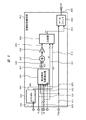
- FIG. 1 is a schematic diagram showing a configuration example of a signal transmission system according to Embodiment 1 of the present invention.
- FIG. 1 shows a configuration example of a signal transmission system that performs wired transmission on the same substrate.
- the substrate 101 includes a signal processing ASIC (Application Specific Integrated Circuit) 102 having a waveform equalization function, a communication ASIC 103 having a waveform equalization function, and a connector 104.
- the ASIC 102 and the ASIC 103 communicate with each other via a wiring on the substrate 101, and the ASIC 103 communicates with another device through the connector 104.
- ASIC Application Specific Integrated Circuit
- FIG. 2 is a schematic diagram showing another configuration example of the signal transmission system according to Embodiment 1 of the present invention.
- FIG. 2 shows a configuration example of a signal transmission system in which the communication in FIG. 1 is performed not only on the same board but also on different boards and a repeater is mounted.
- the substrate 201 mounts the signal processing ASIC 204, the repeater 205, and the connector 208, and the substrate 203 mounts the signal processing ASIC 207, the repeater 206, and the connectors 209 and 210.
- the substrate 202 is connected to the substrates 201 and 203 via connectors 208 and 209, respectively.
- the signal processing ASIC 204 communicates with another device connected to the end of the connector 210 through the communication ASIC 207.
- the signal output from the ASIC 204 is relayed to the board 202 by the relay 205 and transmitted to the relay 206 via the wiring on the board 202.
- the repeater 206 relays the transmitted signal to the communication ASIC 207, and the ASIC 207 transmits the relayed signal to an external device through the connector 210.
- a signal received by the ASIC 207 from the external device through the connector 210 is received by the ASIC 204 via the repeater 206, the substrate 202, and the repeater 205 in this order.
- each of the ASICs 102, 103, 204, 207 and the repeaters 205, 206 is a signal transmission device in which a transmitter and a receiver are mounted on one semiconductor chip, for example.
- the substrate 202 is a backplane or the like
- each of the substrates 201 and 203 is a card or the like that can be mounted on the backplane.
- FIG. 3 is a block diagram illustrating a configuration example of each signal transmission device studied as a premise of the first embodiment in the signal transmission system of FIGS. 1 and 2.
- the semiconductor chips (signal transmission devices) 301 and 303 in FIG. 3 correspond to the ASICs 102 and 103 in FIG. 1, respectively, and the transmission path 302 in FIG. 3 corresponds to the wiring on the substrate 101 in FIG.
- the semiconductor chips 301 and 303 in FIG. 3 correspond to the repeaters 205 and 206 in FIG. 2, respectively, and the transmission path 302 in FIG. 3 corresponds to the wiring on the substrate 202 in FIG.
- the semiconductor chip (signal transmission device) 301 includes a transmitter 304 and a signal processing unit 305
- the semiconductor chip (signal transmission device) 303 includes a receiver 309 and a signal processing unit 310.
- a signal transmitted from the transmitter 304 of the semiconductor chip 301 is transmitted through the transmission path 302 and received by the receiver 309 of the semiconductor chip 303.
- each of the semiconductor chips 301 and 304 is configured to include one of a transmitter and a receiver for convenience, but actually includes both a transmitter and a receiver.
- the transmitter 304 includes a feed forward equalizer (hereinafter referred to as FFE) 307, a multiplexer 306, and a PLL (Phase Locked) Loop) 308.
- the receiver 309 includes a continuous time linear equalizer (hereinafter referred to as CTLE (Continuous Time Linear Equalizer)) 311, a decision feedback equalizer (hereinafter referred to as DFE (Decision Feedback Equalizer)) 312, and a clock source. 313, a filter coefficient calculation unit 314, and a demultiplexer 315.
- CTLE Continuous Time Linear Equalizer
- DFE Decision Feedback Equalizer
- the signal processing unit 305 performs predetermined signal processing and transmits a parallel data signal to the transmitter 304 as necessary.
- the multiplexer (parallel-serial converter) 306 receives the parallel data signal and converts the parallel data signal into a serial data signal in synchronization with the clock from the PLL 308.
- the FFE 307 receives the serial data signal, processes the data signal into a signal that emphasizes the high frequency side in advance, and transmits the signal to the transmission path 302. Specifically, the FFE 307 performs waveform equalization so as to reduce the gain on the low frequency side, for example.
- the data signal 315 that has passed through the transmission path 302 is received by the receiver 309 in the semiconductor chip 303.
- the data signal transmitted from the transmitter 304 is attenuated through the transmission path 302.
- the CTLE 311 performs waveform equalization by amplifying the high-frequency side of the received data signal, and outputs the signal (Vo) 320 on which waveform equalization has been performed to the DFE 312.
- the DFE 312 performs waveform equalization on the signal (Vo) 320 such that the low frequency side is attenuated and the high frequency side is amplified in accordance with the filter coefficient (Wi) 330 from the filter coefficient calculation unit 314 and amplified. After that, logical determination (positive / negative determination) is performed.
- the DFE 312 sequentially latches the logical data (DTS) 325 that is the result of the logical determination (positive / negative determination) in response to the clock 321 from the clock source 313, and outputs it as a serial data signal. Further, the DFE 312 compares not only the logical determination of data but also the filter convergence target value (target peak value) (TGT) 331 from the filter coefficient calculation unit 314 and the peak value of the signal subjected to waveform equalization by the DFE 312. Then, a filter convergence target value error (ERRs) 326 is output.
- DTS logical data
- TGT filter convergence target value
- ERRs filter convergence target value error
- the demultiplexer (serial / parallel converter) 315 receives the logical data (DTS) 325 and the filter convergence target value error (ERRs) 326, and converts these serial signals into parallel signals using the clocks 323 and 324 from the clock source 313. To do. As a result, the demultiplexer 315 outputs logical data (DTP) 327 as a parallel data signal, logical data (DTp) 328 as a part thereof, and a filter convergence target value error (ERRp) 329 as a parallel signal. To do.
- DTP logical data
- DTp logical data
- ERRp filter convergence target value error
- the demultiplexer 315 outputs a parallel signal every 32 cycles of the clock 324.
- the logical data (DTP) 327 is configured by, for example, a 32-bit area
- the logical data (DTp) 328 is configured by a predetermined adjacent multiple-bit area in the 32-bit area.
- the number of bits of the plurality of bits is determined based on the number of taps of the DFE 312, for example.
- the filter coefficient calculation unit 314 receives the logical data (DTp) 328 and the filter convergence target value error (ERRp) 329.
- the logical data (DTS) 325 and the filter convergence target value error (ERRs) 326 from the DFE 312 are input to the filter coefficient calculation unit 314 via the demultiplexer 315.
- the filter coefficient calculation unit 314 operates with the clock 322 from the clock source 313, receives the logical data (DTp) 328 and the filter convergence target value error (ERRp) 329, and sets the filter coefficient (Wi) 330 of the DFE 312 by an adaptive algorithm. calculate.
- an LMS (Least) Mean Square) algorithm is typically known.
- the filter coefficient calculation unit 314 also calculates a filter convergence target value (target peak value) (TGT) 331.
- the filter convergence target value (target peak value) (TGT) 331 can be, for example, an average value of the signal amplitude after waveform equalization (V (Z 0 ) in FIG. 16 described later). That is, when waveform equalization is performed, the signal amplitude after waveform equalization is ideally constant regardless of the data pattern. Therefore, the filter coefficient calculation unit 314 detects the average value of the signal amplitude and uses it as a target value so that the instantaneous amplitude value approaches the target value (that is, the target value error is minimized). An arithmetic process that converges the filter coefficients may be performed using an adaptive algorithm.
- the signal processing unit 310 performs predetermined signal processing using the logical data (DTP) 327.
- DTP logical data
- the signal processing unit 310 performs error correction or the like on the logical data (DTP) 327 and then stores the logical data in the semiconductor chip 303.
- the relaying process is performed via a transmitter (not shown).
- FIG. 16 is a schematic diagram illustrating a schematic configuration example of the DFE in FIG.
- the DFE 312 receives the signal (Vo) 320 from the CTLE 311 and feeds back the multiplication result of the filter coefficient (Wi) 330 and the logical data of the past signal (Vo) 320 to the signal.
- Waveform equalization Here, the case of 3 taps is taken as an example, and the multiplier block 1601 outputs each logical data (Z in the previous to third cycles) output from the determiner with latch 1602, the latch circuit 1603, and the latch circuit 1604, respectively. ⁇ 1 , Z ⁇ 2 , Z ⁇ 3 ) and the first to third tap filter coefficients W1 to W3, respectively.
- the adder block 1600 performs waveform equalization by adding the multiplication result from the multiplier block 1601 to the signal (Vo) 320. This eliminates intersymbol interference (ISI) components.
- ISI intersymbol interference
- the DFE 312 outputs the logical data of the signal (Vo) 320 by performing logical determination (positive / negative determination) and latching of the waveform equalized signal (V (Z 0 )) by the determination unit 1602 with latch.
- the logical data is sequentially transferred to the latch circuit 1603 and the latch circuit 1604 in synchronization with the clock.
- the DFE 312 detects the difference between the wave height value of the waveform equalized signal and the filter convergence target value (target wave height value) (TGT) 331 by the error detector 1605, so that the filter convergence target value error (ERRs) 326 is detected. Is output after adjusting the timing by the delay circuit 1606.
- the CTLE 311 in FIG. 3 is an analog amplifier and has a limited input / output range that can be linearly amplified.
- the power supply voltage decreases, and the input / output range in which linearity can be secured is becoming narrower.
- the power supply voltage is 1 V or less
- the input range in which linear operation is possible with a general resistive load type amplifier is only about 200 to 300 mV, for example.
- the loss in the transmission path 302 on the substrate tends to increase on the high frequency side, and the signal level difference between the low frequency side and the high frequency side increases as the speed increases.
- a signal level difference of 30 dB or more can occur.
- the signal level increases to, for example, 500 mV or more, and the linear operation of the CTLE 311 becomes difficult.
- the signal (Vo) 320 from the CTLE 311 includes components added to the signal due to the influence of nonlinearity in addition to components added to the signal by ISI.
- the component due to ISI depends on the data pattern because it follows the frequency characteristics of the signal path, and the component due to non-linearity depends on the signal level (and hence the frequency of the signal), so it also depends on the data pattern. Both depend on the data pattern, but because the causes are different from each other, the same trend does not occur.
- the filter coefficient calculation unit 314 obtains a correlation between the data pattern (that is, each bit of the logical data (DTp) 328) and the filter convergence target value error (ERRp) 329, and uses the LMS algorithm or the like.
- a filter coefficient (Wi) 330 is calculated.
- the filter coefficient calculation unit 314 is difficult to extract only the ISI component from the correlation result, for example, because the data pattern dependency of the component due to ISI and the component due to nonlinearity do not have the same tendency.
- an error in the calculation result of the filter coefficient (Wi) 330 (that is, an error with respect to an ideal waveform equalization amount necessary for eliminating the ISI component) may occur.
- an error when the filter coefficient (Wi) 330 is automatically adjusted in accordance with environmental fluctuations such as temperature and power supply voltage fluctuations becomes large.
- the waveform equalization amount is deviated, the ISI component cannot be sufficiently eliminated, and there is a possibility that jitter increases (for example, eye reduction in a so-called eye pattern).
- a signal affected by non-linearity is detected, and only a linearly operating signal is used for calculation of the filter coefficient (Wi) 330. Specifically, by not using the low-frequency signal for calculating the filter coefficient (Wi) 330, the influence of nonlinearity is suppressed and the filter coefficient (Wi) 330 is optimally converged.
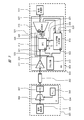
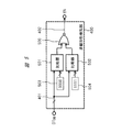
- FIG. 4 is a block diagram illustrating a configuration example of a main part of the signal transmission device according to the first embodiment in the signal transmission system of FIGS. 1 and 2.
- the signal transmission device according to the first embodiment is configured to include a receiver 309 as in the semiconductor chip (signal transmission device) 303 of FIG. 3. As shown in FIG. The configuration is different from FIG.
- the receiver 309 illustrated in FIG. 4 further includes a nonlinearity detection unit 400 with respect to the receiver 309 of FIG.
- the non-linearity detection unit 400 monitors the logical data from the DFE, detects a data pattern in which n bits (n is an integer of 2 or more) are continuously at the same logical level, and causes the filter coefficient calculation unit 314 to detect the detection. Instructed not to calculate the filter coefficient (Wi) 330 for the selected data pattern.
- the nonlinearity detection unit 400 receives the logical data (DTpp) 401 that is a part of the logical data (DTp) 328 from the demultiplexer 315, and thereby monitors the logical data from the DFE.
- the nonlinearity detection unit 400 looks at the data pattern of the logical data (DTpp) 401 and outputs an enable signal (EN) 402 that instructs the filter coefficient calculation unit 314 whether or not to calculate the filter coefficient.
- the loss of the transmission path 302 tends to be low on the low frequency side and high on the high frequency side. Therefore, if a low frequency signal is detected, a signal that is not linearly amplified can be detected.
- the low frequency signal is a case where the same data continues, for example, in the case of a data pattern such as 111..., 000.
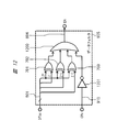
- FIG. 5 is a circuit diagram showing a configuration example of the nonlinearity detection unit in FIG.
- a case where the logical data (DTpp) 401 is 4 bits is taken as an example.
- the nonlinearity detection unit 400 controls the enable signal (EN) 402 to the “L” level (negate) when the comparison results match, and sets the enable signal (EN) 402 to “H” when they do not match. Control to level (assert).
- the nonlinearity detection unit 400 includes a NOR gate 500, comparators 501 and 502, and predetermined data patterns 503 and 504.
- the data pattern of the logical data (DTpp) 401 is “0000”
- the output of the comparator 501 is at the “H” level
- the enable signal (EN) 402 output from the NOR gate 500 is at the “L” level.
- the data pattern of the logical data (DTpp) 401 is “1111”
- the output of the comparator 502 becomes “H” level
- the enable signal (EN) 402 becomes “L” level.
- the filter coefficient calculation unit 314 performs the filter coefficient (Wi) 330 and the filter convergence target value (TGT) for the logical data (DTp) 328 corresponding to the logical data (DTpp) 401 according to the 'L' level. ) The calculation of 331 is stopped.
- FIG. 7 is a circuit diagram showing another configuration example of the nonlinearity detection unit in FIG. 7 receives the logical data (DTpp) 401, the logical data (Z 0 ) of the current cycle included in the logical data (DTpp) 401, and the previous to (n ⁇ 1) ) Each logical data (Z ⁇ 1 to Z ⁇ 3 ) in the previous cycle is compared with each other.
- the nonlinearity detection unit 400 controls the enable signal (EN) 402 to the “L” level (negate) when the comparison results match, and sets the enable signal (EN) 402 to “H” when they do not match. Control to level (assert).
- the nonlinearity detection unit 400 includes an OR gate 700 and three XOR gates 701, 702, and 703.
- the XOR gates 701, 702, and 703 include the logical data (Z 0 ) in the current cycle included in the logical data (DTpp) 401 and the logical data (Z ⁇ 1 to Z ⁇ in the previous to third previous cycles). 3 ) are compared with each other.
- the OR gate 700 outputs the 'L' level as the enable signal (EN) 402 only when all the comparison results match (that is, when the data pattern is “1111” or “0000”).
- the filter coefficient calculation unit 314 stops the calculation of the filter coefficient for the logical data (DTp) 328 corresponding to the logical data (DTpp) 401 according to the “L” level.
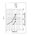
- FIG. 6 is an explanatory diagram showing an example of the effect when the receivers of FIGS. 4 and 5 are used.
- FIG. 6 shows a simulation using a 28 Gbps NRZ signal for a system having a loss of 35 dB at the Nyquist frequency with the bit number (n) of the data patterns 503 and 504 of the nonlinearity detection unit 400 being 4 bits. It is a result.
- the cross marks indicate the results when the nonlinearity detection unit 400 is not provided, and the results when the nonlinearity detection unit 400 is provided.
- the horizontal axis is 1 dB compression point, which is an index indicating the linearity of CTLE 311, and the lower the linearity, the worse the linearity.
- the vertical axis represents the jitter of the signal after waveform equalization in DFE 312 (V (Z 0 ) in FIG. 16).
- the jitter can be reduced by the filter coefficient (Wi) 330 converging to an appropriate value even under poor linearity conditions. That is, by using the signal transmission device and the signal transmission system according to the first embodiment, the filter constant of the DFE 312 can be optimally maintained regardless of the linearity of the amplifier (CTLE 311) in the receiver 309, and jitter can be reduced. Etc. can be realized.
- the number of bits (n) of the data patterns 503 and 504 for example, assuming that the equalization amount in the DFE 312 is 20 dB and the loss increases with a constant slope (dB / Hz), the Nyquist frequency of 28 Gbps is obtained in 32 GFC. At 1/14, the loss becomes 0 dB. In this case, the number of bits (n) of the data patterns 503 and 504 is appropriately about 4 bits that is 1/16 of the data rate.
- the number of bits (n) of the data patterns 503 and 504 is not particularly limited to this and may be 2 bits or more. However, if the number of bits is too small, the signal on the high frequency side is unnecessarily filtered, resulting in poor convergence of the filter coefficient. If the number of bits is too large, the filtering that is originally necessary for some of the signals on the low frequency side is performed. This is not done, and there is a risk of increasing jitter. Therefore, for example, the frequency of the boundary where nonlinearity occurs in the CTLE 311 may be estimated in consideration of the characteristics of the transmitter 304 and the transmission path 302, and the number of bits corresponding to the frequency near the boundary may be determined.
- FIG. 8 is a block diagram showing a configuration example of the main part of the signal transmission apparatus according to the second embodiment.
- FIG. 8 shows a configuration example of the receiver 309 included in the signal transmission device, as in the case of FIG.
- the receiver 309 in FIG. 8 includes a CTLE 311, a DFE 312, a clock source 313, a filter coefficient calculation unit 314, a demultiplexer 315, and a nonlinearity detection unit 800 as in the case of the first embodiment (FIG. 4).
- the configuration and operation of the nonlinearity detection unit 800 are different from those in the first embodiment, and the input / output signals with other circuit blocks are also slightly different. Hereinafter, description will be made focusing on this difference.
- the demultiplexer 315 becomes a part of the logical data (DTp) 328 in addition to the logical data (DTP) 327, the logical data (DTp) 328, and the filter convergence target value error (ERRp) 329 similar to the case of FIG.
- the logical data (DTpp) 801 is output.
- the filter coefficient calculation unit 314 performs the filter coefficient (Wi) 330 and the filter convergence target value (TGT) when the enable signal (EN) 804 from the nonlinearity detection unit 800 is at the “H” level. ) 331 is calculated, and when the enable signal (EN) 804 is at the “L” level, the calculation is stopped.
- the filter coefficient calculation unit 314 outputs the calculated filter coefficient (Wi) 330 and the filter convergence target value (TGT) 331 to the DFE 312, and further outputs the calculated filter coefficient (Wi) 802 to the nonlinearity detection unit 800.
- a filter convergence target value (TGT) 803 is output.
- the nonlinearity detection unit 800 includes a signal (Vo) 320 from the CTLE 311, a logical data (DTpp) 801 from the demultiplexer 315, a filter coefficient (Wi) 802 and a filter convergence target value (TGT) from the filter coefficient calculation unit 314. 803, and operates in synchronization with clocks 805 and 806 from the clock source 313.
- the clock 805 is a clock having the same phase as the clock 321 to the DFE 312, and the clock 806 is an internal operation clock.
- the nonlinearity detection unit of the first embodiment described above detects logical data in which the same logical level is continued for n bits as logical data in which nonlinearity occurs.
- whether or not nonlinearity actually occurs may vary depending on, for example, the length of the transmission path 302.
- the length of the transmission path 302 may vary depending on the mounting position.
- the nonlinearity detection unit 800 in FIG. 8 calculates the filter coefficient for each frequency (on the high frequency side and the low frequency side) in the same manner as the DFE 312 and the filter coefficient calculation unit 314, and the average value of the filter coefficient and the filter coefficient By comparing with the filter coefficient (Wi) 802 from the calculation unit 314, it is determined whether or not the CTLE 311 is operating linearly.
- the enable signal (EN) 804 is kept at the “H” level even when the same logic level continues for n bits, and is not operating linearly.
- the enable signal (EN) 804 is controlled to the 'L' level.
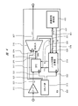
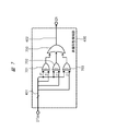
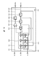
- FIG. 9 is a block diagram illustrating a configuration example of the nonlinearity detection unit in FIG. 9 includes a controller 900, a frequency-specific coefficient detector 901, an adder 902, an amplifier 903, a comparator 904, and a data filter 905.
- the controller 900 operates in synchronization with the clock 806, outputs a detection enable signal (DEN) 906 to the coefficient detector 901 for each frequency for a certain period, and outputs a predetermined threshold value (a predetermined threshold value) to the comparator 904.
- DEN detection enable signal
- Wth predetermined threshold value
- the frequency-specific coefficient detector 901 includes a signal (Vo) 320 from the CTLE 311, a filter coefficient (Wi) 802, and a demultiplexer 315 while the detection enable signal (DEN) 906 is at the “H” level (asserted). In response to the logical data (DTpp) 801, the detection operation is performed in synchronization with the clock 805.
- the frequency-specific coefficient detector 901 includes a dummy decision feedback equalizer and a dummy filter coefficient calculator that reflect the configurations of the DFE 312 and the filter coefficient calculator 314, respectively, as shown in detail in FIG. The filter coefficient corresponding to the tap eye is calculated and held.
- the frequency-specific coefficient detector 901 targets the data pattern in which the logic data of the signal (Vo) 320 from the CTLE 311 is m bits (m is an integer of 2 or more) continuously at the same logic level.
- the dummy filter coefficient (W1l) 907 for the first tap is calculated.
- the frequency-specific coefficient detector 901 calculates a dummy filter coefficient (W1h) 908 for the first tap on the high frequency side for a data pattern that does not have the same logic level continuously for 2 bits or more.
- the logical data (DTpp) 801 from the demultiplexer 315 is used here as the logical data of the signal (Vo) 320 from the CTLE 311. For example, in the case of 3 bits, if the logical data (DTpp) 801 is “000” or “111”, it is determined as a low frequency, and if it is “010” or “101”, it is determined as a high frequency.
- the adder 902 and the amplifier 903 average the low frequency side dummy filter coefficient (W1l) 907 and the high frequency side dummy filter coefficient (W1h) 908, thereby calculating an average value calculation unit that calculates the dummy filter coefficient 909. It becomes. That is, the adder 902 adds the dummy filter coefficient (W1l) 907 on the low frequency side and the dummy filter coefficient (W1h) 908 on the high frequency side, and the amplifier 903 halves the addition result.
- the filter coefficient (Wi) 802 from the filter coefficient calculation unit 314 is an optimal value.
- the dummy filter coefficient 909 should be a value that is not significantly different from the filter coefficient (W1) 911 of the first tap of the filter coefficient (Wi) 802.
- the CTLE 311 cannot operate linearly, the dummy filter coefficient 909 and the filter coefficient (W1) 911 are greatly different.
- the comparator 904 generates the nonlinearity detection signal (CPo) 910 when the absolute value of the difference between the dummy filter coefficient 909 and the filter coefficient (W1) 911 is larger than a predetermined threshold value (Wth) 912.
- the “H” level is output, and if not, the “L” level is output as the non-linearity detection signal (CPo) 910.
- the “H” level of the non-linearity detection signal (CPo) 910 indicates that the CTLE 311 cannot operate linearly.
- the data filter 905 operates when the nonlinearity detection signal (CPo) 910 is at the “H” level, and stops operating when it is at the “L” level.
- the data filter 905 monitors the logical data (DTpp) 801 from the DFE 312 via the demultiplexer 315, and displays a data pattern in which n bits are continuously at the same logical level, and the nonlinearity detection signal (CPo) 910 is 'H'. 'Detect if level.
- the data filter 905 outputs “L” level as the enable signal (EN) 804 during the period when the data pattern is detected, and “H” as the enable signal (EN) 804 during the period when it is not detected. Output level.
- the filter coefficient calculation unit 314 stops the calculation of the filter coefficient for the logical data (DTp) 328 corresponding to the logical data (DTpp) 801 according to the “L” level of the enable signal (EN) 804. .
- the filter coefficient calculation unit 314 calculates a filter coefficient when the enable signal (EN) 804 is at the “H” level.
- the data filter 905 outputs “L” level as the enable signal (EN) 804 when the logical data (DTpp) 801 is “0000” or “1111”, as in the first embodiment. To do.
- the number of high frequency / low frequency discrimination bits (m) in the frequency-specific coefficient detector 901 and the low frequency discrimination bit number (n) in the data filter 905 are not necessarily the same. It does not have to be.
- the presence or absence of the nonlinear operation is determined using the filter coefficient of the first tap of the DFE 312, but the filter coefficients of other taps are used instead of the first tap or in addition to the first tap. Is also possible.
- the use of the first tap in particular makes it possible to determine the presence or absence of nonlinear operation with the highest sensitivity.
- FIG. 10 is a circuit diagram showing a configuration example of the frequency-specific coefficient detector in FIG.
- the frequency coefficient detector 901 includes the dummy DFE 1016 described in FIG. 9 and a dummy filter coefficient calculation unit 1017.
- the dummy DFE 1016 includes a sample and hold circuit 1000, an analog / digital converter 1001, delay circuits 1002 and 1003, multipliers 1004, 1005 and 1009, adders 1006 and 1007, and an amplifier 1008.
- the dummy filter coefficient calculation unit 1017 includes a multiplier 1011, a selector 1012, and integrators 1014 and 1015. In FIG. 10, a case where a 2-tap DFE is used is taken as an example.
- the sample hold circuit 1000 samples the signal (Vo) 320 from the CTLE 311 with the clock 805, and the analog-digital converter 1001 converts the sampled signal into a digital value.
- the phase of the clock 805 is the same as that of the clock 321 for the DFE 312, but the frequency may be less than or equal to the frequency of the clock 321 for the DFE 312. That is, the dummy DFE 1016 may be operated so as to thin out the operation of the DFE 312.
- the delay circuit 1002 delays the digital value from the analog-digital converter 1001 with the clock 805 and outputs it to the adder 1006.
- the delay circuit 1003 delays the logical data (DTpp) 801 from the demultiplexer 315 with the clock 805 and outputs it.
- the delay circuits 1002 and 1006 output the digital value of the signal (Vo) 320 in the current cycle from the delay circuit 1002, and the signal (Vo) 320 in the current cycle and the past cycle.
- the timing at which the logic data (DTpp) 801 is output from the delay circuit 1003 coincides. Since the logical data (DTpp) 801 is generated by the DFE 312 and input to the dummy DFE 1016 via the demultiplexer 315, such timing adjustment is performed.
- the multipliers 1004 and 1005 and the adder 1006 are feedback units that perform waveform equalization.
- the multipliers 1004 and 1005 are connected to the logical data (Z ⁇ 1 and Z ⁇ 2 ) of the past cycle (here, the previous and second previous cycles) included in the logical data (DTpp) 801 from the delay circuit 1003.
- the filter coefficient (Wi) 802 (here, the first tap and the second tap) from the filter coefficient calculation unit 314 is multiplied.
- the adder 1006 adds the digital value (D (Z 0 )) from the delay circuit 1002 and the multiplication result from the multipliers 1004 and 1005, so that the signal (Vo) 320 (the digital value thereof) of the current cycle is added. Waveform equalization is performed on (D (Z 0 )).
- the amplifier 1008, the multiplier 1009, and the adder 1007 serve as an error calculation unit that calculates an error between the peak value after waveform equalization and the target peak value.
- the amplifier 1008 multiplies the logical data (Z 0 ) (positive / negative data) of the current cycle included in the logical data (DTpp) 801 from the delay circuit 1003 by ⁇ 1, and the multiplier 1009 calculates the output of the amplifier 1008 and the filter
- the filter convergence target value (target peak value) (TGT) 803 from the coefficient calculation unit 314 is multiplied.
- the adder 1007 adds the digital value after waveform equalization from the adder 1006 and the digital value from the multiplier 1009 to calculate an error between the peak values of both.
- the multiplier 1011 outputs the logical data (Z ⁇ 1 ) of the past cycle (here, the previous cycle) included in the logical data (DTpp) 801 from the delay circuit 1003. And the digital value from the adder 1007 are multiplied.
- the difference between the peak value of the signal (Vo) 320 and the filter convergence target value (TGT) 803 can be correlated with the logical data of the previous cycle, and 1 is obtained by integrating the result.
- the filter coefficient at the tap can be calculated.
- the selector (selection unit) 1012 selects one of the integrators 1014 and 1015 according to the logical data (DTpp) 801 from the delay circuit 1003, and the digital value from the multiplier 1011 is sent to the selected integrator. Output. Specifically, the selector 1012 indicates that the logical data (DTpp) 801 is “000” or “111” (in other words, the logical data of the signal (Vo) 320 from the DFE 312 is the same logical level for m bits continuously.
- the integrator 1014 is selected. That is, the selector 1012 outputs the digital value from the multiplier 1011 for the data pattern on the low frequency side to the integrator 1014.
- the selector 1012 when the logical data (DTpp) 801 is “010” or “101” (in other words, the logical data of the signal (Vo) 320 from the DFE 312 is not continuously at the same logical level for 2 bits or more. Case), integrator 1015 is selected. That is, the selector 1012 outputs the digital value from the multiplier 1011 targeted for the high frequency side data pattern to the integrator 1015. Note that the selector 1012 does not output to the integrators 1014 and 1015 when the data pattern of the logical data (DTpp) 801 is other than these.
- the integrator 1014 integrates the digital value for the data pattern on the low frequency side from the selector 1012 in synchronization with the clock 805 during the period when the detection enable signal (DEN) 906 is at the “H” level.
- the frequency side dummy filter coefficient (W1l) 907 is calculated.
- the integrator 1015 integrates the digital value for the data pattern on the high frequency side from the selector 1012 in synchronism with the clock 805 during the period in which the detection enable signal (DEN) 906 is at the “H” level.
- the dummy filter coefficient (W1h) 908 is calculated. Further, the integrators 1014 and 1015 hold the integration results while the detection enable signal (DEN) 906 is at the ‘L’ level.
- FIG. 11 is a circuit diagram showing a configuration example of the data filter in FIG.
- a data filter 905 of FIG. 11 includes an OR gate 1100 and an inverter 1101 in addition to the NOR gate 500, the comparators 501 and 502, and the data patterns 503 and 504 similar to those in FIG. Similar to the case of FIG. 5, the comparator 501 compares the logical data (DTpp) 801 with the data pattern 503 “0000”, and the comparator 502 compares the logical data (DTpp) 801 with the data pattern “1111”. 503 is compared.
- the NOR gate 500 outputs the ‘L’ level when the data pattern of the logical data (DTpp) 801 is “0000” or “1111”.
- the inverter 1101 inverts the nonlinearity detection signal (CPo) 910.
- the OR gate 1100 is when the output of the inverter 1101 is at the “L” level (that is, when the nonlinearity detection signal (CPo) 910 is at the “H” level), and when the output of the NOR gate 500 is at the “L” level.
- the “L” level is output as the enable signal (EN) 804.
- FIG. 12 is a circuit diagram showing another configuration example of the data filter in FIG.
- the data filter 905 in FIG. 12 includes an OR gate 1200 and an inverter 1201 in addition to the XOR gates 701, 702, and 703 similar to those in FIG.
- the XOR gates 701, 702, and 703 operate with the logical data (DTpp) 801 as input, as in the case of FIG.
- the inverter 1201 inverts the nonlinearity detection signal (CPo) 910.
- the OR gate 1200 receives the outputs of the XOR gates 701, 702, and 703, and additionally receives the output of the inverter 1201.
- the OR gate 1200 enables the enable signal when the nonlinearity detection signal (CPo) 910 is at the “H” level and the data pattern of the logical data (DTpp) 801 is “0000” or “1111”. (EN) Output 'L' level as 804.
- the data pattern to be calculated for the filter coefficient can be determined more accurately. Therefore, the jitter may be further reduced.
- FIG. 13 is a block diagram showing a configuration example of the main part of the signal transmission apparatus according to the third embodiment.
- FIG. 13 shows a configuration example of the nonlinearity detection unit 800 in the receiver 309 included in the signal transmission device, as in FIG.
- the nonlinearity detection unit 800 shown in FIG. 13 differs from the configuration example of FIG. 9 in the configuration and operation of the controller 1300 and the frequency-specific coefficient detector 1301.
- the controller 1300 outputs logical data for detection (DPN) 1302 in addition to the detection enable signal (DEN) 906 similar to the case of FIG.
- the frequency coefficient detector 1301 detects a filter coefficient for each frequency based on the detection logic data (DPN) 1302.
- an analog-digital converter 1001 is used in the frequency-specific coefficient detector 901 in FIG. 10. Since the analog-digital converter 1001 is required to operate at high speed, there is a risk of increasing power consumption and complicating the circuit. Therefore, it is desirable not to use an analog-digital converter. However, in this case, it is necessary to perform waveform equalization on the analog signal in real time. In other words, when the analog-digital converter 1001 is used, the analog signal of the current cycle is converted into a digital value, and then a delay is added. Waveform equalization can be performed after waiting for logical data of the past cycle. Adding a delay to the signal itself is not easy.
- the controller 1300 generates the low-frequency side data pattern and the high-frequency side data pattern as described in the second embodiment, and generates the generated data patterns in different periods.
- the frequency-specific coefficient detector 1301 speculatively executes the operations up to immediately before the final stage integrators (1407 and 1408 in FIG. 14 described later) based on the detection logic data (DPN) 1302, and performs actual logic processing.
- the integrator is operated.
- FIG. 15 is a flowchart showing an example of the operation sequence of the controller in FIG.
- a case where the detection logical data (DPN) 1302 is 3 bits is taken as an example.
- the controller 1300 sets the detection logic data (DPN) 1302 to “000” (step S1501), sets the detection enable signal (DEN) 906 to the “H” level, and sets the coefficient detector for each frequency 1301. Operate (step S1502).
- the controller 1300 operates the coefficient detector for each frequency 1301 for a certain period of time to detect a peak value error or the like when a data pattern of “000” is assumed (step S1503).
- the controller 1300 sets the detection logical data (DPN) 1302 to “111” (step S1504), operates the frequency-specific coefficient detector 1301 for a certain period of time, and assumes a data pattern of “111”. In this case, a peak value error or the like is detected (step S1505). Subsequently, the controller 1300 sets the detection logical data (DPN) 1302 to “010” (step S1506), operates the frequency-specific coefficient detector 1301 for a certain period of time, and assumes a data pattern of “010”. In this case, a peak value error or the like is detected (step S1507).
- the controller 1300 sets the detection logical data (DPN) 1302 to “101” (step S1508), operates the frequency-specific coefficient detector 1301 for a certain period of time, and assumes a data pattern of “101”. In this case, a peak value error or the like is detected (step S1509). Thereafter, the controller 1300 sets the detection enable signal (DEN) 906 to the 'L' level and stops the operation of the frequency coefficient detector 1301 (step S1510). As described above, the controller 1300 includes the detection logical data (“000” or “111”) in which the same logical level continues for m bits and the detection logical data (“010” in which the same logical level does not continue for 2 bits or more). "Or” 101 ”) are output in different periods.
- FIG. 14 is a circuit diagram showing a configuration example of the frequency-specific coefficient detector in FIG.
- the frequency-specific coefficient detector 1301 roughly indicates that the filter coefficient when the detection logical data (DPN) 1302 matches the logical data (DTpp) 801 input from the DFE 312 via the demultiplexer 315. Is calculated.
- the frequency-specific coefficient detector 1301 includes a dummy DFE 1419 and a dummy filter coefficient calculation unit 1420.
- the dummy DFE 1419 includes adders 1400 and 1401, a determiner 1402, a latch circuit 1403, multipliers 1409, 1410 and 1414, an amplifier 1413, and digital / analog converters 1411, 1412 and 1415.
- the dummy filter coefficient calculation unit 1420 includes a multiplier 1404, a delay circuit 1415, a selector 1406, integrators 1407 and 1408, and an integrator control unit 1421.
- the integrator control unit 1421 includes a delay circuit 1416, a comparator 1417, and an AND gate 1418.
- Multipliers 1409 and 1410, digital-analog converters 1411 and 1412, and adder 1400 serve as a feedback unit that performs waveform equalization.
- Multipliers 1409 and 1410 include respective bits corresponding to the past cycles (here, the previous and second previous cycles) included in the detection logical data (DPN) 1302 from the controller 1300, and a filter coefficient calculation unit.
- the filter coefficient (Wi) 802 from 314 (here, the first tap and the second tap) is multiplied.
- Digital-to-analog converters 1411 and 1412 convert digital values resulting from multiplication by multipliers 1409 and 1410 to analog signals (filter constants), respectively.
- the adder 1400 performs waveform equalization by adding the analog signals from the digital-analog converters 1411 and 1412 to the signal (Vo) 320 from the CTLE 311.
- the amplifier 1413, the multiplier 1414, the digital-analog converter 1415, and the adder 1401 serve as an error detection unit that detects an error between the peak value after waveform equalization and the target peak value.
- the amplifier 1413 multiplies the bit (positive / negative data) corresponding to the current cycle included in the detection logic data (DPN) 1302 by ⁇ 1, and the multiplier 1414 outputs the output from the amplifier 1413 and the filter coefficient calculation unit 314.
- the filter convergence target value (target peak value) (TGT) 803 is multiplied.
- the digital / analog converter 1415 converts the digital value from the multiplier 1414 into an analog signal (that is, an analog signal corresponding to the target peak value).
- the adder 1401 adds the analog signal from the adder 1400 (that is, the analog signal after waveform equalization) and the analog signal from the digital-analog converter 1415, and outputs the difference signal.
- the determiner 1402 determines whether the difference signal from the adder 1401 is positive or negative (that is, determines whether the analog signal after waveform equalization is larger or smaller than the target), and the latch circuit 1403 displays the determination result at the clock 805. Latch.
- the multiplier 1404 includes the logic data (Z ⁇ 1 ) of the past cycle (here, the previous cycle) included in the detection logic data (DPN) 1302 and the latch circuit. Multiply the logical data from 1403.
- the delay circuit 1405 delays the logical data from the multiplier 1404 with the clock 805.
- the selector (selection unit) 1406 outputs the logic data from the delay circuit 1405 to the integrator 1407 when the detection logic data (DPN) 1302 is a low frequency data pattern (“000” or “111”). .
- the selector 1406 outputs the logical data from the delay circuit 1405 to the integrator 1408 when the detection logical data (DPN) 1302 is a high-frequency data pattern (“010” or “101”).
- the selector 1406 does not output to the integrators 1407 and 1408 when the detection logical data (DPN) 1302 is other than these.
- the delay circuit 1416 delays the logical data (DTpp) 801 input from the DFE 312 via the demultiplexer 315 with the clock 805.
- the comparator 1417 compares the logical data (DTpp) 801 from the delay circuit 1416 with the detection logical data (DPN) 1302 and outputs an 'H' level if they match.
- the AND gate 1418 outputs the “H” level as the integration enable signal (IEN) 1422 when the detection enable signal (DEN) 906 is at the “H” level and the comparator 1417 outputs the “H” level. Is output.
- the timing at which the processing result for the signal (Vo) 320 of the current cycle from the CLTE 311 is output from the delay circuit 1405 by the delay circuits 1405 and 1416 and the logical data of each signal (Vo) 320 in the current cycle and the past cycle The timing at which (DTpp) 801 is output from the delay circuit 1416 coincides.
- the integrator 1407 integrates logic data based on the data pattern on the low frequency side from the selector 1406 in synchronization with the clock 805 in a period in which the integration enable signal (IEN) 1422 is at the “H” level.
- a dummy filter coefficient (W1l) 907 on the low frequency side is calculated.
- the integrator 1408 integrates the logic data based on the data pattern on the high frequency side from the selector 1406 in synchronization with the clock 805 in a period in which the integration enable signal (IEN) 1422 is at the “H” level.
- Side dummy filter coefficient (W1l) 908 is calculated. Further, the integrators 1407 and 1408 hold the integration results while the integration enable signal (IEN) 1422 is at the ‘L’ level.
- speculatively executed data based on the detection logic data (DPN) 1302 has reached the inputs of the integrators 1407 and 1408.
- This data becomes correct data when the detection logical data (DPN) 1302 and the logical data (DTpp) 801 match, and becomes incorrect data when they do not match. Therefore, by identifying this match / mismatch (in other words, whether speculative execution is correct) by the integration enable signal (IEN) 1422, only correct data can be integrated by the integrators 1407, 1408.
- an analog-digital converter is not necessary, so that power consumption can be reduced. In some cases, the circuit can be simplified.
- the present invention made by the present inventor has been specifically described based on the embodiment.
- the present invention is not limited to the embodiment, and various modifications can be made without departing from the scope of the invention.
- the above-described embodiment has been described in detail for easy understanding of the present invention, and is not necessarily limited to one having all the configurations described.
- a part of the configuration of one embodiment can be replaced with the configuration of another embodiment, and the configuration of another embodiment can be added to the configuration of one embodiment. .
Landscapes
- Engineering & Computer Science (AREA)
- Computer Networks & Wireless Communication (AREA)
- Signal Processing (AREA)
- Cable Transmission Systems, Equalization Of Radio And Reduction Of Echo (AREA)
Abstract
A continuous time linear equalizer (CTLE) 311 outputs a second signal that has been waveform-equalized by amplifying the higher frequency side of an input first signal. A decision feedback equalizer (DFE) 312 waveform-equalizes the input second signal by use of a filter factor (Wi) and makes a logic decision on the waveform-equalized second signal to thereby output logic data of the second signal (DTS), and further, the DFE 312 detects a difference between a peak value of the waveform-equalized signal and a target peak value (TGT) to thereby output a target value error (ERRs). A filter factor calculation unit 314 receives the logic data and target value error from the DFE 312 and calculates a filter factor (Wi) of the DFE 312 by use of an adaptive algorithm. A nonlinearity detection unit 400 monitors the logic data from the DFE 312, detects a data pattern of n bits (where n is an integer equal to or greater than two) successively having the same logic level, and instructs the filter factor calculation unit 314 not to perform the filter factor calculation for the detected data pattern.
Description
本発明は、信号伝送装置および信号伝送システムに関し、例えば、高速有線伝送向け受信機における等化器の等化量を自動収束させる技術に関する。
The present invention relates to a signal transmission device and a signal transmission system, for example, a technique for automatically converging the equalization amount of an equalizer in a receiver for high-speed wired transmission.
近年、ストリーミングの普及やクラウドサービスの普及などにより通信量が増加傾向にあり、それに対応して情報機器のデータ量の増加および処理能力の向上が進展している。その際に、大規模データ処理のボトルネックとなる装置内外の通信速度も同様に向上しつつある。例えば、装置外の通信では、100G Etherや32GFCといった規格への対応が進みつつあり、1レーン辺り25Gbps、28Gbpsの通信速度へと高速化が進展している。
In recent years, the amount of communication has been increasing due to the spread of streaming and the spread of cloud services, and in response to this, the increase in the amount of data in information devices and the improvement of processing capacity are progressing. At that time, the communication speed inside and outside the apparatus, which is a bottleneck for large-scale data processing, is also improving. For example, in communication outside the apparatus, support for standards such as 100G Ether and 32GFC is progressing, and speeding up is progressing to communication speeds of 25 Gbps and 28 Gbps per lane.
通信の高速化により、例えば基板の損失は増え、14GHzで35dB以上の損失が見込まれており、さらにインピーダンスミスマッチによる反射の影響も無視できなくなってきている(非特許文献1参照)。そのため、ジッタをできるだけ抑える必要があり、等化器のフィルタ定数を環境変動に対して適応させてジッタの増加を抑える技術が重要である。従来、入力データパターンに応じてメモリに蓄えておいた応答を出力して等化する技術があり、その応答パターンを環境変動に応じて適応させるという技術も提案されている(非特許文献2参照)。
With the increase in communication speed, for example, the loss of the substrate is increased, a loss of 35 dB or more is expected at 14 GHz, and the influence of reflection due to impedance mismatch cannot be ignored (see Non-Patent Document 1). For this reason, it is necessary to suppress jitter as much as possible, and a technique for suppressing an increase in jitter by adapting the filter constant of the equalizer to environmental fluctuations is important. Conventionally, there is a technique for outputting a response stored in a memory according to an input data pattern and equalizing it, and a technique for adapting the response pattern according to an environmental change has been proposed (see Non-Patent Document 2). ).
通信の高速化により基板上やケーブルの経路損失が増えており、低周波と高周波で信号の振幅差が増大する傾向にある。これにより、受信機の入力信号の振幅差は、送信機のデータパターンに応じて増大する。一方、SNR(Signal to Noise Ratio)を確保するため、送信機の送信信号の振幅は大きくせざるを得ない。これらの結果、受信機の入力信号を増幅する増幅器には、広い入出力範囲で線形増幅を行う(すなわち高線形性を実現する)ことが要求される。しかし、高速動作に対応するため、例えば、微細CMOS(Complementary Metal-Oxide-Semiconductor)プロセスを用いると、電源電圧を低くする必要がある。そうすると、増幅器の高線形性を実現することは困難となり得る。
Acceleration of communication has increased the path loss on the board and cable, and the signal amplitude difference tends to increase at low and high frequencies. Thereby, the amplitude difference of the input signal of the receiver increases in accordance with the data pattern of the transmitter. On the other hand, in order to secure SNR (Signal to Noise Ratio), the amplitude of the transmission signal of the transmitter must be increased. As a result, an amplifier that amplifies the input signal of the receiver is required to perform linear amplification in a wide input / output range (that is, to achieve high linearity). However, in order to cope with high-speed operation, for example, when a fine CMOS (Complementary Metal-Oxide-Semiconductor) process is used, it is necessary to lower the power supply voltage. If so, it may be difficult to achieve high linearity of the amplifier.
高線形性を実現できない場合、増幅器からの出力信号には、非線形性による成分と、ISI(Inter Symbol Interference)による成分とが混在することになる。この2つの成分は、共にデータパターンに依存するが、それぞれ異なるメカニズムで生成されるため関数が異なる。このように、相関があり関数の異なる2つの成分を互いに分離することは容易でない。一方、増幅器からの出力信号は、等化器で等化される。等化器は、ISI成分を低減するため、フィルタ係数を環境変動に応じて自動調整する。しかし、増幅器からの出力信号には前述した2つの成分が混在しているため、等化器でフィルタ係数を自動調整する際の誤差が大きくなる場合がある。この場合、フィルタ係数の収束値は理想からずれてしまい、必要な等化量が得られず(すなわちISI成分を低減できず)、ジッタが増大する恐れがある。
If high linearity cannot be realized, the output signal from the amplifier will contain both non-linear components and ISI (Inter Symbol Interference) components. These two components both depend on the data pattern, but have different functions because they are generated by different mechanisms. As described above, it is not easy to separate two components having a correlation and different functions. On the other hand, the output signal from the amplifier is equalized by an equalizer. The equalizer automatically adjusts the filter coefficient according to environmental fluctuations in order to reduce the ISI component. However, since the above-mentioned two components are mixed in the output signal from the amplifier, there may be a case where an error when the filter coefficient is automatically adjusted by the equalizer is increased. In this case, the convergence value of the filter coefficient is deviated from the ideal value, and a necessary equalization amount cannot be obtained (that is, the ISI component cannot be reduced), and the jitter may increase.
本発明は、このようなことに鑑みてなされたものであり、その目的の一つは、ジッタの低減を実現可能な信号伝送装置および信号伝送システムを提供することにある。
The present invention has been made in view of such circumstances, and one of its purposes is to provide a signal transmission device and a signal transmission system capable of realizing jitter reduction.
本発明の前記並びにその他の目的と新規な特徴は、本明細書の記述及び添付図面から明らかになるであろう。
The above and other objects and novel features of the present invention will become apparent from the description of the present specification and the accompanying drawings.
本願において開示される発明のうち、代表的な実施の形態の概要を簡単に説明すれば、次のとおりである。
Among the inventions disclosed in the present application, the outline of a typical embodiment will be briefly described as follows.
本実施の形態による信号伝送装置は、連続時間線形等化器と、判定帰還型等化器と、フィルタ係数計算部と、非線形性検知部とを有する。連続時間線形等化器は、入力された第1信号の高周波側を増幅することで波形等化が行われた第2信号を出力する。判定帰還型等化器は、入力された第2信号をフィルタ係数を用いて波形等化し、それを論理判定することで第2信号の論理データを出力し、かつ波形等化した信号の波高値と目標波高値との差分を検出することで目標値誤差を出力する。フィルタ係数計算部は、判定帰還型等化器からの論理データおよび目標値誤差が入力され、適応アルゴリズムによって判定帰還型等化器のフィルタ係数を算出する。非線形性検知部は、判定帰還型等化器からの論理データを監視し、nビット(nは2以上の整数)連続して同一の論理レベルとなるデータパターンを検知し、フィルタ係数計算部に、当該検知したデータパターンを対象とするフィルタ係数の算出を行わないように指示する。
The signal transmission apparatus according to the present embodiment includes a continuous-time linear equalizer, a decision feedback equalizer, a filter coefficient calculation unit, and a nonlinearity detection unit. The continuous time linear equalizer outputs a second signal subjected to waveform equalization by amplifying the high frequency side of the input first signal. The decision feedback equalizer equalizes the waveform of the input second signal using a filter coefficient, outputs the logical data of the second signal by logically determining the waveform, and the peak value of the waveform equalized signal The target value error is output by detecting the difference between the target value and the target peak value. The filter coefficient calculation unit receives the logical data and the target value error from the decision feedback equalizer, and calculates the filter coefficient of the decision feedback equalizer using an adaptive algorithm. The non-linearity detection unit monitors the logical data from the decision feedback equalizer, detects a data pattern in which n bits (n is an integer of 2 or more) are continuously at the same logical level, and outputs the data pattern to the filter coefficient calculation unit. And instructing not to calculate a filter coefficient for the detected data pattern.
本願において開示される発明のうち、代表的な実施の形態によって得られる効果を簡単に説明すると、ジッタの低減が実現可能になる。
A brief description of the effect obtained by the representative embodiment of the invention disclosed in the present application makes it possible to reduce jitter.
以下の実施の形態においては便宜上その必要があるときは、複数のセクションまたは実施の形態に分割して説明するが、特に明示した場合を除き、それらは互いに無関係なものではなく、一方は他方の一部または全部の変形例、詳細、補足説明等の関係にある。また、以下の実施の形態において、要素の数等(個数、数値、量、範囲等を含む)に言及する場合、特に明示した場合および原理的に明らかに特定の数に限定される場合等を除き、その特定の数に限定されるものではなく、特定の数以上でも以下でも良い。
In the following embodiment, when it is necessary for the sake of convenience, the description will be divided into a plurality of sections or embodiments. However, unless otherwise specified, they are not irrelevant, and one is the other. Some or all of the modifications, details, supplementary explanations, and the like are related. Further, in the following embodiments, when referring to the number of elements (including the number, numerical value, quantity, range, etc.), especially when clearly indicated and when clearly limited to a specific number in principle, etc. Except, it is not limited to the specific number, and may be more or less than the specific number.
さらに、以下の実施の形態において、その構成要素(要素ステップ等も含む)は、特に明示した場合および原理的に明らかに必須であると考えられる場合等を除き、必ずしも必須のものではないことは言うまでもない。同様に、以下の実施の形態において、構成要素等の形状、位置関係等に言及するときは、特に明示した場合および原理的に明らかにそうでないと考えられる場合等を除き、実質的にその形状等に近似または類似するもの等を含むものとする。このことは、上記数値および範囲についても同様である。
Further, in the following embodiments, the constituent elements (including element steps and the like) are not necessarily indispensable unless otherwise specified and apparently essential in principle. Needless to say. Similarly, in the following embodiments, when referring to the shapes, positional relationships, etc. of the components, etc., the shapes are substantially the same unless otherwise specified, or otherwise apparent in principle. And the like are included. The same applies to the above numerical values and ranges.
また、実施の形態の各機能ブロックを構成する回路素子は、特に制限されないが、公知のCMOS(相補型MOSトランジスタ)等の集積回路技術によって、単結晶シリコンのような半導体基板上に形成される。
The circuit elements constituting each functional block of the embodiment are not particularly limited, but are formed on a semiconductor substrate such as single crystal silicon by a known integrated circuit technology such as a CMOS (complementary MOS transistor). .
以下、本発明の実施の形態を図面に基づいて詳細に説明する。なお、実施の形態を説明するための全図において、同一の部材には原則として同一の符号を付し、その繰り返しの説明は省略する。
Hereinafter, embodiments of the present invention will be described in detail with reference to the drawings. Note that components having the same function are denoted by the same reference symbols throughout the drawings for describing the embodiment, and the repetitive description thereof will be omitted.
(実施の形態1)
《信号伝送システムの概略構成》
図1は、本発明の実施の形態1による信号伝送システムにおいて、その構成例を示す概略図である。図1には、同一基板上での有線伝送を行う信号伝送システムの構成例が示される。基板101は、波形等化機能を有する信号処理用ASIC(Application Specific Integrated Circuit)102と、波形等化機能を有する通信用ASIC103と、コネクタ104とを搭載する。ASIC102とASIC103とは、基板101上の配線を介して互いに通信を行い、ASIC103は、コネクタ104を通じて別の機器と通信を行う。 (Embodiment 1)
<< Schematic configuration of signal transmission system >>
FIG. 1 is a schematic diagram showing a configuration example of a signal transmission system according toEmbodiment 1 of the present invention. FIG. 1 shows a configuration example of a signal transmission system that performs wired transmission on the same substrate. The substrate 101 includes a signal processing ASIC (Application Specific Integrated Circuit) 102 having a waveform equalization function, a communication ASIC 103 having a waveform equalization function, and a connector 104. The ASIC 102 and the ASIC 103 communicate with each other via a wiring on the substrate 101, and the ASIC 103 communicates with another device through the connector 104.
《信号伝送システムの概略構成》
図1は、本発明の実施の形態1による信号伝送システムにおいて、その構成例を示す概略図である。図1には、同一基板上での有線伝送を行う信号伝送システムの構成例が示される。基板101は、波形等化機能を有する信号処理用ASIC(Application Specific Integrated Circuit)102と、波形等化機能を有する通信用ASIC103と、コネクタ104とを搭載する。ASIC102とASIC103とは、基板101上の配線を介して互いに通信を行い、ASIC103は、コネクタ104を通じて別の機器と通信を行う。 (Embodiment 1)
<< Schematic configuration of signal transmission system >>
FIG. 1 is a schematic diagram showing a configuration example of a signal transmission system according to
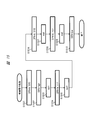
図2は、本発明の実施の形態1による信号伝送システムにおいて、その別の構成例を示す概略図である。図2には、図1での通信を同一基板だけでなく別々の基板で行い、なおかつ中継器が搭載される信号伝送システムの構成例が示される。基板201は、信号処理用ASIC204と中継器205とコネクタ208とを搭載し、基板203は、信号処理用ASIC207と中継器206とコネクタ209,210とを搭載する。基板202は、コネクタ208,209を介して基板201,203にそれぞれ接続される。
FIG. 2 is a schematic diagram showing another configuration example of the signal transmission system according to Embodiment 1 of the present invention. FIG. 2 shows a configuration example of a signal transmission system in which the communication in FIG. 1 is performed not only on the same board but also on different boards and a repeater is mounted. The substrate 201 mounts the signal processing ASIC 204, the repeater 205, and the connector 208, and the substrate 203 mounts the signal processing ASIC 207, the repeater 206, and the connectors 209 and 210. The substrate 202 is connected to the substrates 201 and 203 via connectors 208 and 209, respectively.
図1での信号の流れと同様に、信号処理用ASIC204は、通信用ASIC207を通してコネクタ210の先に接続されている別の機器と通信を行う。この際に、ASIC204から出力された信号は、中継器205によって基板202に中継され、基板202上の配線を介して中継器206に伝送される。中継器206は、伝送された信号を通信用ASIC207に中継し、ASIC207は、中継された信号をコネクタ210を通して外部の機器へと伝達する。逆に、外部の機器からコネクタ210を通してASIC207で受信された信号は、中継器206、基板202、中継器205を順に介してASIC204で受信される。
As in the signal flow in FIG. 1, the signal processing ASIC 204 communicates with another device connected to the end of the connector 210 through the communication ASIC 207. At this time, the signal output from the ASIC 204 is relayed to the board 202 by the relay 205 and transmitted to the relay 206 via the wiring on the board 202. The repeater 206 relays the transmitted signal to the communication ASIC 207, and the ASIC 207 transmits the relayed signal to an external device through the connector 210. Conversely, a signal received by the ASIC 207 from the external device through the connector 210 is received by the ASIC 204 via the repeater 206, the substrate 202, and the repeater 205 in this order.
図1および図2において、ASIC102,103,204,207や中継器205,206のそれぞれは、例えば、1個の半導体チップに送信機および受信機を搭載した信号伝送装置である。また、図2において、例えば、基板202は、バックプレーン等であり、基板201,203のそれぞれは、当該バックプレーンに装着可能なカード等である。
1 and 2, each of the ASICs 102, 103, 204, 207 and the repeaters 205, 206 is a signal transmission device in which a transmitter and a receiver are mounted on one semiconductor chip, for example. In FIG. 2, for example, the substrate 202 is a backplane or the like, and each of the substrates 201 and 203 is a card or the like that can be mounted on the backplane.
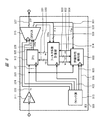
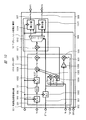
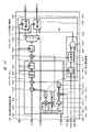
《信号伝送装置の前提構成》
図3は、図1および図2の信号伝送システムにおいて、本実施の形態1の前提として検討した各信号伝送装置の構成例を示すブロック図である。一例として、図3の半導体チップ(信号伝送装置)301,303は、それぞれ、図1のASIC102,103に該当し、図3の伝送路302は、図1の基板101上の配線に該当する。また別の例として、図3の半導体チップ301,303は、それぞれ、図2の中継器205,206に該当し、図3の伝送路302は、図2の基板202上の配線に該当する。 << Prerequisite configuration of signal transmission equipment >>
FIG. 3 is a block diagram illustrating a configuration example of each signal transmission device studied as a premise of the first embodiment in the signal transmission system of FIGS. 1 and 2. As an example, the semiconductor chips (signal transmission devices) 301 and 303 in FIG. 3 correspond to the ASICs 102 and 103 in FIG. 1, respectively, and the transmission path 302 in FIG. 3 corresponds to the wiring on the substrate 101 in FIG. As another example, the semiconductor chips 301 and 303 in FIG. 3 correspond to the repeaters 205 and 206 in FIG. 2, respectively, and the transmission path 302 in FIG. 3 corresponds to the wiring on the substrate 202 in FIG.
図3は、図1および図2の信号伝送システムにおいて、本実施の形態1の前提として検討した各信号伝送装置の構成例を示すブロック図である。一例として、図3の半導体チップ(信号伝送装置)301,303は、それぞれ、図1のASIC102,103に該当し、図3の伝送路302は、図1の基板101上の配線に該当する。また別の例として、図3の半導体チップ301,303は、それぞれ、図2の中継器205,206に該当し、図3の伝送路302は、図2の基板202上の配線に該当する。 << Prerequisite configuration of signal transmission equipment >>
FIG. 3 is a block diagram illustrating a configuration example of each signal transmission device studied as a premise of the first embodiment in the signal transmission system of FIGS. 1 and 2. As an example, the semiconductor chips (signal transmission devices) 301 and 303 in FIG. 3 correspond to the
半導体チップ(信号伝送装置)301は、送信機304および信号処理部305を備え、半導体チップ(信号伝送装置)303は、受信機309および信号処理部310を備える。半導体チップ301の送信機304から送信された信号は、伝送路302を伝送し、半導体チップ303の受信機309で受信される。ここでは、半導体チップ301,304のそれぞれは、便宜上、送信機および受信機の一方を備える構成となっているが、実際には、送信機および受信機の両方を備える。
The semiconductor chip (signal transmission device) 301 includes a transmitter 304 and a signal processing unit 305, and the semiconductor chip (signal transmission device) 303 includes a receiver 309 and a signal processing unit 310. A signal transmitted from the transmitter 304 of the semiconductor chip 301 is transmitted through the transmission path 302 and received by the receiver 309 of the semiconductor chip 303. Here, each of the semiconductor chips 301 and 304 is configured to include one of a transmitter and a receiver for convenience, but actually includes both a transmitter and a receiver.
送信機304は、フィードフォワードイコライザ(以降、FFEと呼ぶ)307と、マルチプレクサ306と、PLL(Phase Locked Loop)308とを備える。受信機309は、連続時間線形等化器(以降、CTLE(Continuous Time Linear Equalizer)と呼ぶ)311と、判定帰還型等化器(以降、DFE(Decision Feedback Equalizer)と呼ぶ)312と、クロック源313と、フィルタ係数計算部314と、デマルチプレクサ315とを備える。
The transmitter 304 includes a feed forward equalizer (hereinafter referred to as FFE) 307, a multiplexer 306, and a PLL (Phase Locked) Loop) 308. The receiver 309 includes a continuous time linear equalizer (hereinafter referred to as CTLE (Continuous Time Linear Equalizer)) 311, a decision feedback equalizer (hereinafter referred to as DFE (Decision Feedback Equalizer)) 312, and a clock source. 313, a filter coefficient calculation unit 314, and a demultiplexer 315.
次に、図3の動作について説明する。まず、信号処理部305は、所定の信号処理を行い、必要に応じてパラレルデータ信号を送信機304に送信する。マルチプレクサ(パラレルシリアル変換器)306は、当該パラレルデータ信号を受信し、PLL308からのクロックに同期してパラレルデータ信号をシリアルデータ信号に変換する。FFE307は、当該シリアルデータ信号を受信し、当該データ信号を、予め高周波側を強調した信号に加工したのち伝送路302に送信する。具体的には、FFE307は、例えば、低周波側のゲインを落とすように波形等化を行う。
Next, the operation of FIG. 3 will be described. First, the signal processing unit 305 performs predetermined signal processing and transmits a parallel data signal to the transmitter 304 as necessary. The multiplexer (parallel-serial converter) 306 receives the parallel data signal and converts the parallel data signal into a serial data signal in synchronization with the clock from the PLL 308. The FFE 307 receives the serial data signal, processes the data signal into a signal that emphasizes the high frequency side in advance, and transmits the signal to the transmission path 302. Specifically, the FFE 307 performs waveform equalization so as to reduce the gain on the low frequency side, for example.
伝送路302を通ったデータ信号315は、半導体チップ303内の受信機309で受信される。この際に、送信機304から送信されたデータ信号は、伝送路302を通って減衰している。CTLE311は、受信したデータ信号の高周波側を増幅することで波形等化を行い、波形等化が行われた信号(Vo)320をDFE312に出力する。DFE312は、信号(Vo)320に対して、フィルタ係数計算部314からのフィルタ係数(Wi)330に従って低周波側を減衰させ高周波側を増幅されるような波形等化を行い、それを増幅した後、論理判定(正負判定)を行う。
The data signal 315 that has passed through the transmission path 302 is received by the receiver 309 in the semiconductor chip 303. At this time, the data signal transmitted from the transmitter 304 is attenuated through the transmission path 302. The CTLE 311 performs waveform equalization by amplifying the high-frequency side of the received data signal, and outputs the signal (Vo) 320 on which waveform equalization has been performed to the DFE 312. The DFE 312 performs waveform equalization on the signal (Vo) 320 such that the low frequency side is attenuated and the high frequency side is amplified in accordance with the filter coefficient (Wi) 330 from the filter coefficient calculation unit 314 and amplified. After that, logical determination (positive / negative determination) is performed.
そして、DFE312は、クロック源313からのクロック321で当該論理判定(正負判定)結果となる論理データ(DTS)325を順次ラッチし、シリアルデータ信号として出力する。さらに、DFE312は、データの論理判定のみでなく、フィルタ係数計算部314からのフィルタ収束目標値(目標波高値)(TGT)331と、DFE312で波形等化を行った信号の波高値とを比較し、フィルタ収束目標値誤差(ERRs)326を出力する。
The DFE 312 sequentially latches the logical data (DTS) 325 that is the result of the logical determination (positive / negative determination) in response to the clock 321 from the clock source 313, and outputs it as a serial data signal. Further, the DFE 312 compares not only the logical determination of data but also the filter convergence target value (target peak value) (TGT) 331 from the filter coefficient calculation unit 314 and the peak value of the signal subjected to waveform equalization by the DFE 312. Then, a filter convergence target value error (ERRs) 326 is output.
デマルチプレクサ(シリアルパラレル変換器)315は、論理データ(DTS)325とフィルタ収束目標値誤差(ERRs)326とを受け、これらのシリアル信号をクロック源313からのクロック323,324でパラレル信号に変換する。これにより、デマルチプレクサ315は、パラレルデータ信号となる論理データ(DTP)327と、その一部となる論理データ(DTp)328と、パラレル信号となるフィルタ収束目標値誤差(ERRp)329とを出力する。
The demultiplexer (serial / parallel converter) 315 receives the logical data (DTS) 325 and the filter convergence target value error (ERRs) 326, and converts these serial signals into parallel signals using the clocks 323 and 324 from the clock source 313. To do. As a result, the demultiplexer 315 outputs logical data (DTP) 327 as a parallel data signal, logical data (DTp) 328 as a part thereof, and a filter convergence target value error (ERRp) 329 as a parallel signal. To do.
例えば、クロック323がクロック324の1/32の周波数を持つ場合、デマルチプレクサ315は、クロック324の32サイクル毎にパラレル信号を出力する。この場合、論理データ(DTP)327は、例えば、32ビットの領域で構成され、論理データ(DTp)328は、当該32ビットの領域の中の、予め定めた隣接する複数ビットの領域で構成される。当該複数ビットのビット数は、例えば、DFE312のタップ数に基づいて定められる。
For example, when the clock 323 has a frequency 1/32 that of the clock 324, the demultiplexer 315 outputs a parallel signal every 32 cycles of the clock 324. In this case, the logical data (DTP) 327 is configured by, for example, a 32-bit area, and the logical data (DTp) 328 is configured by a predetermined adjacent multiple-bit area in the 32-bit area. The The number of bits of the plurality of bits is determined based on the number of taps of the DFE 312, for example.
フィルタ係数計算部314には、論理データ(DTp)328およびフィルタ収束目標値誤差(ERRp)329が入力される。言い換えれば、フィルタ係数計算部314には、DFE312からの論理データ(DTS)325およびフィルタ収束目標値誤差(ERRs)326がデマルチプレクサ315を介して入力される。フィルタ係数計算部314は、クロック源313からのクロック322で動作し、論理データ(DTp)328およびフィルタ収束目標値誤差(ERRp)329を受けて、適応アルゴリズムによってDFE312のフィルタ係数(Wi)330を算出する。適応アルゴリズムとして、代表的には、LMS(Least Mean Square)アルゴリズムが知られている。
The filter coefficient calculation unit 314 receives the logical data (DTp) 328 and the filter convergence target value error (ERRp) 329. In other words, the logical data (DTS) 325 and the filter convergence target value error (ERRs) 326 from the DFE 312 are input to the filter coefficient calculation unit 314 via the demultiplexer 315. The filter coefficient calculation unit 314 operates with the clock 322 from the clock source 313, receives the logical data (DTp) 328 and the filter convergence target value error (ERRp) 329, and sets the filter coefficient (Wi) 330 of the DFE 312 by an adaptive algorithm. calculate. As an adaptive algorithm, an LMS (Least) Mean Square) algorithm is typically known.
さらに、フィルタ係数計算部314は、フィルタ収束目標値(目標波高値)(TGT)331の算出も行う。フィルタ収束目標値(目標波高値)(TGT)331は、例えば、波形等化後の信号振幅(後述する図16のV(Z0))の平均値とすることができる。すなわち、波形等化を行った場合、波形等化後の信号振幅は、理想的には、データパターンに依らず一定となる。そこで、フィルタ係数計算部314は、当該信号振幅の平均値を検出し、それを目標値として瞬時的な振幅値が当該目標値に近づくように(すなわち目標値誤差が最小となるように)、適応アルゴリズムを用いてフィルタ係数を収束させるような演算処理を行えばよい。
Furthermore, the filter coefficient calculation unit 314 also calculates a filter convergence target value (target peak value) (TGT) 331. The filter convergence target value (target peak value) (TGT) 331 can be, for example, an average value of the signal amplitude after waveform equalization (V (Z 0 ) in FIG. 16 described later). That is, when waveform equalization is performed, the signal amplitude after waveform equalization is ideally constant regardless of the data pattern. Therefore, the filter coefficient calculation unit 314 detects the average value of the signal amplitude and uses it as a target value so that the instantaneous amplitude value approaches the target value (that is, the target value error is minimized). An arithmetic process that converges the filter coefficients may be performed using an adaptive algorithm.
信号処理部310は、論理データ(DTP)327を用いて所定の信号処理を行う。例えば、半導体チップ303が図2の中継器205等の場合、信号処理部310は、論理データ(DTP)327に対して、エラー訂正等の処理を行ったのち、当該論理データを半導体チップ303内の図示しない送信機を介して中継するような処理を行う。
The signal processing unit 310 performs predetermined signal processing using the logical data (DTP) 327. For example, when the semiconductor chip 303 is the repeater 205 in FIG. 2, the signal processing unit 310 performs error correction or the like on the logical data (DTP) 327 and then stores the logical data in the semiconductor chip 303. The relaying process is performed via a transmitter (not shown).
図16は、図3におけるDFEの模式的な構成例を示す概略図である。図16に示すように、DFE312は、CTLE311からの信号(Vo)320が入力され、当該信号に、フィルタ係数(Wi)330と過去の信号(Vo)320の論理データとの乗算結果を帰還することで波形等化を行う。ここでは、3タップの場合を例とし、乗算器ブロック1601は、ラッチ付き判定器1602、ラッチ回路1603、ラッチ回路1604からそれぞれ出力される1つ前~3つ前のサイクルにおける各論理データ(Z-1,Z-2,Z-3)と、1タップ目~3タップ目のフィルタ係数W1~W3とをそれぞれ乗算する。加算器ブロック1600は、信号(Vo)320に乗算器ブロック1601からの乗算結果を加算することで波形等化を行う。これによって、符号間干渉(ISI)の成分を排除することができる。
FIG. 16 is a schematic diagram illustrating a schematic configuration example of the DFE in FIG. As shown in FIG. 16, the DFE 312 receives the signal (Vo) 320 from the CTLE 311 and feeds back the multiplication result of the filter coefficient (Wi) 330 and the logical data of the past signal (Vo) 320 to the signal. Waveform equalization. Here, the case of 3 taps is taken as an example, and the multiplier block 1601 outputs each logical data (Z in the previous to third cycles) output from the determiner with latch 1602, the latch circuit 1603, and the latch circuit 1604, respectively. −1 , Z −2 , Z −3 ) and the first to third tap filter coefficients W1 to W3, respectively. The adder block 1600 performs waveform equalization by adding the multiplication result from the multiplier block 1601 to the signal (Vo) 320. This eliminates intersymbol interference (ISI) components.
また、DFE312は、当該波形等化した信号(V(Z0))を、ラッチ付き判定器1602で論理判定(正負判定)およびラッチすることで信号(Vo)320の論理データを出力する。当該論理データは、クロックに同期して、順に、ラッチ回路1603、ラッチ回路1604に転送される。さらに、DFE312は、波形等化した信号の波高値と、フィルタ収束目標値(目標波高値)(TGT)331との差分を誤差検出器1605で検出することでフィルタ収束目標値誤差(ERRs)326を生成し、それを、遅延回路1606でタイミング調整を行ったのち出力する。
Further, the DFE 312 outputs the logical data of the signal (Vo) 320 by performing logical determination (positive / negative determination) and latching of the waveform equalized signal (V (Z 0 )) by the determination unit 1602 with latch. The logical data is sequentially transferred to the latch circuit 1603 and the latch circuit 1604 in synchronization with the clock. Further, the DFE 312 detects the difference between the wave height value of the waveform equalized signal and the filter convergence target value (target wave height value) (TGT) 331 by the error detector 1605, so that the filter convergence target value error (ERRs) 326 is detected. Is output after adjusting the timing by the delay circuit 1606.
《信号伝送装置(前提構成)の問題点の一例》
以上のような構成および動作において、図3のCTLE311は、アナログ増幅器となっており、線形的に増幅できる入出力範囲が限られている。また、高速化に伴い微細CMOSプロセスを用いることで、電源電圧が低下し、線形性の確保できる入出力範囲が狭くなってきている。例えば、28nmのCMOSプロセスでは、電源電圧は1V以下となっており、一般的な抵抗負荷型の増幅器だと線形動作可能な入力範囲は、例えば200~300mV程度しかない。 << Examples of problems with signal transmission equipment (prerequisite configuration) >>
In the configuration and operation as described above, theCTLE 311 in FIG. 3 is an analog amplifier and has a limited input / output range that can be linearly amplified. In addition, with the use of a fine CMOS process as the speed increases, the power supply voltage decreases, and the input / output range in which linearity can be secured is becoming narrower. For example, in a 28 nm CMOS process, the power supply voltage is 1 V or less, and the input range in which linear operation is possible with a general resistive load type amplifier is only about 200 to 300 mV, for example.
以上のような構成および動作において、図3のCTLE311は、アナログ増幅器となっており、線形的に増幅できる入出力範囲が限られている。また、高速化に伴い微細CMOSプロセスを用いることで、電源電圧が低下し、線形性の確保できる入出力範囲が狭くなってきている。例えば、28nmのCMOSプロセスでは、電源電圧は1V以下となっており、一般的な抵抗負荷型の増幅器だと線形動作可能な入力範囲は、例えば200~300mV程度しかない。 << Examples of problems with signal transmission equipment (prerequisite configuration) >>
In the configuration and operation as described above, the
さらに、基板上の伝送路302での損失は、高周波側が大きくなる傾向があり、高速化に伴って低周波側と高周波側との信号レベル差が大きくなる。28Gbpsでは、非特許文献1にあるように、30dB以上の信号レベル差が生じ得る。一方、高周波側のSNRを確保するため、送信振幅は小さくできず、伝送路302での損失が小さい低周波側では、信号レベルが例えば500mV以上と大きくなり、CTLE311の線形動作は難しくなる。その結果、CTLE311からの信号(Vo)320には、ISIにより信号に加えられる成分の他に、非線形性の影響により信号に加えられる成分が混在する。
Furthermore, the loss in the transmission path 302 on the substrate tends to increase on the high frequency side, and the signal level difference between the low frequency side and the high frequency side increases as the speed increases. At 28 Gbps, as described in Non-Patent Document 1, a signal level difference of 30 dB or more can occur. On the other hand, since the SNR on the high frequency side is ensured, the transmission amplitude cannot be reduced, and on the low frequency side where the loss in the transmission path 302 is small, the signal level increases to, for example, 500 mV or more, and the linear operation of the CTLE 311 becomes difficult. As a result, the signal (Vo) 320 from the CTLE 311 includes components added to the signal due to the influence of nonlinearity in addition to components added to the signal by ISI.
ISIによる成分は、信号経路の周波数特性に従うためデータパターンに依存し、非線形性による成分は信号レベル(ひいては信号の周波数)に従うため、これもデータパターンに依存する。両者ともデータパターンに依存するが、お互いに原因が異なるため、同傾向にはならない。フィルタ係数計算部314は、例えば、データパターン(すなわち、論理データ(DTp)328の各ビット)と、フィルタ収束目標値誤差(ERRp)329との相関を取り、LMSアルゴリズム等を用いて各タップのフィルタ係数(Wi)330を計算する。
The component due to ISI depends on the data pattern because it follows the frequency characteristics of the signal path, and the component due to non-linearity depends on the signal level (and hence the frequency of the signal), so it also depends on the data pattern. Both depend on the data pattern, but because the causes are different from each other, the same trend does not occur. For example, the filter coefficient calculation unit 314 obtains a correlation between the data pattern (that is, each bit of the logical data (DTp) 328) and the filter convergence target value error (ERRp) 329, and uses the LMS algorithm or the like. A filter coefficient (Wi) 330 is calculated.
この際に、フィルタ係数計算部314は、ISIによる成分と非線形性による成分のデータパターン依存性が同傾向ではないため、例えば、相関結果からISI成分のみを抽出するようなことは困難である。その結果、フィルタ係数(Wi)330の算出結果に誤差(すなわち、ISI成分を排除するのに必要な理想的な波形等化量に対する誤差)が生じ得る。特に、フィルタ係数(Wi)330を温度や電源電圧変動などの環境変動に適応して自動調整する際の誤差が大きくなる。このように、波形等化量にずれが生じると、ISI成分を十分に排除することができず、ジッタの増大(例えば、所謂アイパターンにおけるアイの縮小)等が発生する恐れがある。
At this time, the filter coefficient calculation unit 314 is difficult to extract only the ISI component from the correlation result, for example, because the data pattern dependency of the component due to ISI and the component due to nonlinearity do not have the same tendency. As a result, an error in the calculation result of the filter coefficient (Wi) 330 (that is, an error with respect to an ideal waveform equalization amount necessary for eliminating the ISI component) may occur. In particular, an error when the filter coefficient (Wi) 330 is automatically adjusted in accordance with environmental fluctuations such as temperature and power supply voltage fluctuations becomes large. As described above, when the waveform equalization amount is deviated, the ISI component cannot be sufficiently eliminated, and there is a possibility that jitter increases (for example, eye reduction in a so-called eye pattern).
《信号伝送装置(本実施の形態1)の構成》
ここで、有線伝送においては低周波で損失が小さく高周波で損失が大きくなるため、CTLE311の線形性の影響は、低周波側の信号で大きく、高周波側の信号で小さい。また、非線形性による影響はISIに比べ急峻となる。この場合、信号レベルが小さく線形性の影響の小さい信号をフィルタ係数(Wi)330の収束に用いれば、非線形性による成分の影響を排除し、十分にISI成分のみを抽出可能であると考えられる。そこで、本実施の形態1では、非線形性の影響を受けた信号を検知して、線形動作している信号のみをフィルタ係数(Wi)330の算出に用いる。具体的には、低周波側の信号をフィルタ係数(Wi)330の算出に用いないことで、非線形性の影響を抑制し、フィルタ係数(Wi)330を最適に収束させる。 << Configuration of Signal Transmission Device (Embodiment 1) >>
Here, in wired transmission, loss is low at low frequencies and loss is high at high frequencies. Therefore, the influence of the linearity ofCTLE 311 is large for signals on the low frequency side and small for signals on the high frequency side. In addition, the effect of nonlinearity is steeper than ISI. In this case, if a signal having a small signal level and a small influence of linearity is used for convergence of the filter coefficient (Wi) 330, it is considered that the influence of the component due to the nonlinearity can be eliminated and only the ISI component can be extracted sufficiently. . Therefore, in the first embodiment, a signal affected by non-linearity is detected, and only a linearly operating signal is used for calculation of the filter coefficient (Wi) 330. Specifically, by not using the low-frequency signal for calculating the filter coefficient (Wi) 330, the influence of nonlinearity is suppressed and the filter coefficient (Wi) 330 is optimally converged.
ここで、有線伝送においては低周波で損失が小さく高周波で損失が大きくなるため、CTLE311の線形性の影響は、低周波側の信号で大きく、高周波側の信号で小さい。また、非線形性による影響はISIに比べ急峻となる。この場合、信号レベルが小さく線形性の影響の小さい信号をフィルタ係数(Wi)330の収束に用いれば、非線形性による成分の影響を排除し、十分にISI成分のみを抽出可能であると考えられる。そこで、本実施の形態1では、非線形性の影響を受けた信号を検知して、線形動作している信号のみをフィルタ係数(Wi)330の算出に用いる。具体的には、低周波側の信号をフィルタ係数(Wi)330の算出に用いないことで、非線形性の影響を抑制し、フィルタ係数(Wi)330を最適に収束させる。 << Configuration of Signal Transmission Device (Embodiment 1) >>
Here, in wired transmission, loss is low at low frequencies and loss is high at high frequencies. Therefore, the influence of the linearity of
図4は、図1および図2の信号伝送システムにおいて、本実施の形態1による信号伝送装置の主要部の構成例を示すブロック図である。本実施の形態1による信号伝送装置は、図3の半導体チップ(信号伝送装置)303と同様に受信機309を備えた構成となっており、図4に示すように、当該受信機309の内部構成が図3とは異なっている。図4に示す受信機309は、図3の受信機309に対して、さらに、非線形性検知部400を備える。
FIG. 4 is a block diagram illustrating a configuration example of a main part of the signal transmission device according to the first embodiment in the signal transmission system of FIGS. 1 and 2. The signal transmission device according to the first embodiment is configured to include a receiver 309 as in the semiconductor chip (signal transmission device) 303 of FIG. 3. As shown in FIG. The configuration is different from FIG. The receiver 309 illustrated in FIG. 4 further includes a nonlinearity detection unit 400 with respect to the receiver 309 of FIG.
非線形性検知部400は、DFEからの論理データを監視し、nビット(nは2以上の整数)連続して同一の論理レベルとなるデータパターンを検知し、フィルタ係数計算部314に、当該検知したデータパターンを対象とするフィルタ係数(Wi)330の算出を行わないように指示する。ここでは、非線形性検知部400は、デマルチプレクサ315からの論理データ(DTp)328の一部となる論理データ(DTpp)401を受け、これによって、DFEからの論理データを監視する。非線形性検知部400は、論理データ(DTpp)401のデータパターンを見て、フィルタ係数計算部314に、フィルタ係数の算出を行わせるか否かを指示するイネーブル信号(EN)402を出力する。
The non-linearity detection unit 400 monitors the logical data from the DFE, detects a data pattern in which n bits (n is an integer of 2 or more) are continuously at the same logical level, and causes the filter coefficient calculation unit 314 to detect the detection. Instructed not to calculate the filter coefficient (Wi) 330 for the selected data pattern. Here, the nonlinearity detection unit 400 receives the logical data (DTpp) 401 that is a part of the logical data (DTp) 328 from the demultiplexer 315, and thereby monitors the logical data from the DFE. The nonlinearity detection unit 400 looks at the data pattern of the logical data (DTpp) 401 and outputs an enable signal (EN) 402 that instructs the filter coefficient calculation unit 314 whether or not to calculate the filter coefficient.
前述したように、有線伝送においては、伝送路302の損失が低周波側では低く、高周波側では高いという傾向がある。そのため、低周波信号を検出すれば線形増幅されていない信号を検出することができる。低周波信号は、同一データが連続する場合であり、例えばNRZ(Non Return to Zero)信号であれば、同一の論理レベルがnビット連続する111…、000…といったデータパターンの場合である。
As described above, in wired transmission, the loss of the transmission path 302 tends to be low on the low frequency side and high on the high frequency side. Therefore, if a low frequency signal is detected, a signal that is not linearly amplified can be detected. The low frequency signal is a case where the same data continues, for example, in the case of a data pattern such as 111..., 000.
《非線形性検知部の構成》
図5は、図4における非線形性検知部の構成例を示す回路図である。図5では、論理データ(DTpp)401が4ビットの場合を例とする。当該非線形性検知部400は、論理データ(DTpp)401と、予め定めたnビット(ここではn=4)の論理データ(“0000”または“1111”)とを比較する。当該非線形性検知部400は、比較結果が一致する場合にはイネーブル信号(EN)402を‘L’レベル(ネゲート)に制御し、不一致の場合には、イネーブル信号(EN)402を‘H’レベル(アサート)に制御する。 <Configuration of nonlinearity detection unit>
FIG. 5 is a circuit diagram showing a configuration example of the nonlinearity detection unit in FIG. In FIG. 5, a case where the logical data (DTpp) 401 is 4 bits is taken as an example. Thenonlinearity detection unit 400 compares the logical data (DTpp) 401 with predetermined n-bit (here, n = 4) logical data (“0000” or “1111”). The nonlinearity detection unit 400 controls the enable signal (EN) 402 to the “L” level (negate) when the comparison results match, and sets the enable signal (EN) 402 to “H” when they do not match. Control to level (assert).
図5は、図4における非線形性検知部の構成例を示す回路図である。図5では、論理データ(DTpp)401が4ビットの場合を例とする。当該非線形性検知部400は、論理データ(DTpp)401と、予め定めたnビット(ここではn=4)の論理データ(“0000”または“1111”)とを比較する。当該非線形性検知部400は、比較結果が一致する場合にはイネーブル信号(EN)402を‘L’レベル(ネゲート)に制御し、不一致の場合には、イネーブル信号(EN)402を‘H’レベル(アサート)に制御する。 <Configuration of nonlinearity detection unit>
FIG. 5 is a circuit diagram showing a configuration example of the nonlinearity detection unit in FIG. In FIG. 5, a case where the logical data (DTpp) 401 is 4 bits is taken as an example. The
具体的には、非線形性検知部400は、NORゲート500、比較器501,502、および予め定めたデータパターン503,504で構成される。論理データ(DTpp)401のデータパターンが“0000”の場合、比較器501の出力は‘H’レベルとなり、NORゲート500から出力されるイネーブル信号(EN)402は‘L’レベルとなる。同様に、論理データ(DTpp)401のデータパターンが“1111”の場合、比較器502の出力は‘H’レベルとなり、イネーブル信号(EN)402は‘L’レベルとなる。フィルタ係数計算部314は、当該‘L’レベルに応じて、当該論理データ(DTpp)401に対応する論理データ(DTp)328を対象とする、フィルタ係数(Wi)330およびフィルタ収束目標値(TGT)331の算出を停止する。
Specifically, the nonlinearity detection unit 400 includes a NOR gate 500, comparators 501 and 502, and predetermined data patterns 503 and 504. When the data pattern of the logical data (DTpp) 401 is “0000”, the output of the comparator 501 is at the “H” level, and the enable signal (EN) 402 output from the NOR gate 500 is at the “L” level. Similarly, when the data pattern of the logical data (DTpp) 401 is “1111”, the output of the comparator 502 becomes “H” level, and the enable signal (EN) 402 becomes “L” level. The filter coefficient calculation unit 314 performs the filter coefficient (Wi) 330 and the filter convergence target value (TGT) for the logical data (DTp) 328 corresponding to the logical data (DTpp) 401 according to the 'L' level. ) The calculation of 331 is stopped.
図7は、図4における非線形性検知部の別の構成例を示す回路図である。図7の非線形性検知部400は、論理データ(DTpp)401を受けて、当該論理データ(DTpp)401に含まれる現在のサイクルの論理データ(Z0)と、1つ前~(n-1)つ前のサイクルにおける各論理データ(Z-1~Z-3)のそれぞれとを比較する。当該非線形性検知部400は、比較結果が一致する場合にはイネーブル信号(EN)402を‘L’レベル(ネゲート)に制御し、不一致の場合には、イネーブル信号(EN)402を‘H’レベル(アサート)に制御する。
FIG. 7 is a circuit diagram showing another configuration example of the nonlinearity detection unit in FIG. 7 receives the logical data (DTpp) 401, the logical data (Z 0 ) of the current cycle included in the logical data (DTpp) 401, and the previous to (n−1) ) Each logical data (Z −1 to Z −3 ) in the previous cycle is compared with each other. The nonlinearity detection unit 400 controls the enable signal (EN) 402 to the “L” level (negate) when the comparison results match, and sets the enable signal (EN) 402 to “H” when they do not match. Control to level (assert).
具体的には、当該非線形性検知部400は、ORゲート700と、3個のXORゲート701,702,703を備える。XORゲート701,702,703は、論理データ(DTpp)401に含まれる現在のサイクルの論理データ(Z0)と、1つ前~3つ前のサイクルにおける各論理データ(Z-1~Z-3)とをそれぞれ比較する。ORゲート700は、当該比較結果が全て一致する場合(すなわち、データパターンが“1111”または“0000”の場合)のみで、イネーブル信号(EN)402として‘L’レベルを出力する。フィルタ係数計算部314は、当該‘L’レベルに応じて、当該論理データ(DTpp)401に対応する論理データ(DTp)328を対象とする、フィルタ係数の算出を停止する。
Specifically, the nonlinearity detection unit 400 includes an OR gate 700 and three XOR gates 701, 702, and 703. The XOR gates 701, 702, and 703 include the logical data (Z 0 ) in the current cycle included in the logical data (DTpp) 401 and the logical data (Z −1 to Z − in the previous to third previous cycles). 3 ) are compared with each other. The OR gate 700 outputs the 'L' level as the enable signal (EN) 402 only when all the comparison results match (that is, when the data pattern is “1111” or “0000”). The filter coefficient calculation unit 314 stops the calculation of the filter coefficient for the logical data (DTp) 328 corresponding to the logical data (DTpp) 401 according to the “L” level.
《本実施の形態1の主要な効果》
図6は、図4および図5の受信機を用いた場合の効果の一例を示す説明図である。図6は、非線形性検知部400のデータパターン503,504のビット数(n)を4ビットとし、ナイキスト周波数において35dBの損失がある系に対して、28GbpsのNRZ信号を用いてシミュレーションを行った結果である。図6中で、バツ印の点は、非線形性検知部400を備えない場合の結果であり、非線形性検知部400を備える場合の結果である。また、図6において、横軸は、CTLE311の線形性を示す指標である1dB compression pointであり、低いほど線形性が悪い。縦軸は、DFE312における波形等化後の信号(図16のV(Z0))のジッタを表している。 << Main effects of the first embodiment >>
FIG. 6 is an explanatory diagram showing an example of the effect when the receivers of FIGS. 4 and 5 are used. FIG. 6 shows a simulation using a 28 Gbps NRZ signal for a system having a loss of 35 dB at the Nyquist frequency with the bit number (n) of the data patterns 503 and 504 of the nonlinearity detection unit 400 being 4 bits. It is a result. In FIG. 6, the cross marks indicate the results when the nonlinearity detection unit 400 is not provided, and the results when the nonlinearity detection unit 400 is provided. In FIG. 6, the horizontal axis is 1 dB compression point, which is an index indicating the linearity of CTLE 311, and the lower the linearity, the worse the linearity. The vertical axis represents the jitter of the signal after waveform equalization in DFE 312 (V (Z 0 ) in FIG. 16).
図6は、図4および図5の受信機を用いた場合の効果の一例を示す説明図である。図6は、非線形性検知部400のデータパターン503,504のビット数(n)を4ビットとし、ナイキスト周波数において35dBの損失がある系に対して、28GbpsのNRZ信号を用いてシミュレーションを行った結果である。図6中で、バツ印の点は、非線形性検知部400を備えない場合の結果であり、非線形性検知部400を備える場合の結果である。また、図6において、横軸は、CTLE311の線形性を示す指標である1dB compression pointであり、低いほど線形性が悪い。縦軸は、DFE312における波形等化後の信号(図16のV(Z0))のジッタを表している。 << Main effects of the first embodiment >>
FIG. 6 is an explanatory diagram showing an example of the effect when the receivers of FIGS. 4 and 5 are used. FIG. 6 shows a simulation using a 28 Gbps NRZ signal for a system having a loss of 35 dB at the Nyquist frequency with the bit number (n) of the
図6に示すように、非線形性検知部400を備えることで、線形性が悪い条件でもフィルタ係数(Wi)330が適切な値に収束することにより、ジッタを低減できる。すなわち、本実施の形態1の信号伝送装置および信号伝送システムを用いることで、受信機309中の増幅器(CTLE311)の線形性によらずDFE312のフィルタ定数を最適に保つことができ、ジッタの低減等が実現可能になる。
As shown in FIG. 6, by providing the nonlinearity detection unit 400, the jitter can be reduced by the filter coefficient (Wi) 330 converging to an appropriate value even under poor linearity conditions. That is, by using the signal transmission device and the signal transmission system according to the first embodiment, the filter constant of the DFE 312 can be optimally maintained regardless of the linearity of the amplifier (CTLE 311) in the receiver 309, and jitter can be reduced. Etc. can be realized.
なお、データパターン503,504のビット数(n)に関し、例えば、DFE312での等化量を20dBとし、一定の傾き(dB/Hz)で損失が増えるとすると、32GFCでは、28Gbpsのナイキスト周波数の1/14で損失が0dBとなる。この場合、データパターン503,504のビット数(n)は、データレートの1/16となる4ビット程度が適切となる。
Regarding the number of bits (n) of the data patterns 503 and 504, for example, assuming that the equalization amount in the DFE 312 is 20 dB and the loss increases with a constant slope (dB / Hz), the Nyquist frequency of 28 Gbps is obtained in 32 GFC. At 1/14, the loss becomes 0 dB. In this case, the number of bits (n) of the data patterns 503 and 504 is appropriately about 4 bits that is 1/16 of the data rate.
ただし、データパターン503,504のビット数(n)は、特にこれに限定されず、2ビット以上であればよい。ただし、ビット数が少なすぎると高周波側の信号が不必要にフィルタリングされるため、フィルタ係数の収束性が悪くなり、ビット数が多すぎると低周波側の信号の一部で本来必要なフィルタリングが行われず、ジッタの増大を招く恐れがある。したがって、例えば、送信機304や伝送路302の特性等を踏まえた上でCTLE311で非線形性が生じる境界の周波数を見積もり、当該境界付近の周波数に対応するビット数に定めるとよい。
However, the number of bits (n) of the data patterns 503 and 504 is not particularly limited to this and may be 2 bits or more. However, if the number of bits is too small, the signal on the high frequency side is unnecessarily filtered, resulting in poor convergence of the filter coefficient. If the number of bits is too large, the filtering that is originally necessary for some of the signals on the low frequency side is performed. This is not done, and there is a risk of increasing jitter. Therefore, for example, the frequency of the boundary where nonlinearity occurs in the CTLE 311 may be estimated in consideration of the characteristics of the transmitter 304 and the transmission path 302, and the number of bits corresponding to the frequency near the boundary may be determined.
(実施の形態2)
《信号伝送装置(変形例)の構成》
図8は、本実施の形態2による信号伝送装置において、その主要部の構成例を示すブロック図である。図8には、図4の場合と同様に、信号伝送装置が備える受信機309の構成例が示される。図8の受信機309は、実施の形態1(図4)の場合と同様に、CTLE311、DFE312、クロック源313、フィルタ係数計算部314、デマルチプレクサ315、および非線形性検知部800を備える。ただし、実施の形態1の場合とは非線形性検知部800の構成および動作が異なっており、これに伴い、その他の回路ブロックとの間の入出力信号も若干異なっている。以下、この違いに着目して説明を行う。 (Embodiment 2)
<< Configuration of Signal Transmission Device (Modification) >>
FIG. 8 is a block diagram showing a configuration example of the main part of the signal transmission apparatus according to the second embodiment. FIG. 8 shows a configuration example of thereceiver 309 included in the signal transmission device, as in the case of FIG. The receiver 309 in FIG. 8 includes a CTLE 311, a DFE 312, a clock source 313, a filter coefficient calculation unit 314, a demultiplexer 315, and a nonlinearity detection unit 800 as in the case of the first embodiment (FIG. 4). However, the configuration and operation of the nonlinearity detection unit 800 are different from those in the first embodiment, and the input / output signals with other circuit blocks are also slightly different. Hereinafter, description will be made focusing on this difference.
《信号伝送装置(変形例)の構成》
図8は、本実施の形態2による信号伝送装置において、その主要部の構成例を示すブロック図である。図8には、図4の場合と同様に、信号伝送装置が備える受信機309の構成例が示される。図8の受信機309は、実施の形態1(図4)の場合と同様に、CTLE311、DFE312、クロック源313、フィルタ係数計算部314、デマルチプレクサ315、および非線形性検知部800を備える。ただし、実施の形態1の場合とは非線形性検知部800の構成および動作が異なっており、これに伴い、その他の回路ブロックとの間の入出力信号も若干異なっている。以下、この違いに着目して説明を行う。 (Embodiment 2)
<< Configuration of Signal Transmission Device (Modification) >>
FIG. 8 is a block diagram showing a configuration example of the main part of the signal transmission apparatus according to the second embodiment. FIG. 8 shows a configuration example of the
デマルチプレクサ315は、図4の場合と同様の論理データ(DTP)327、論理データ(DTp)328およびフィルタ収束目標値誤差(ERRp)329に加えて、論理データ(DTp)328の一部となる論理データ(DTpp)801を出力する。フィルタ係数計算部314は、図4の場合と同様に、非線形性検知部800からのイネーブル信号(EN)804が‘H’レベルの場合に、フィルタ係数(Wi)330およびフィルタ収束目標値(TGT)331の算出を行い、イネーブル信号(EN)804が‘L’レベルの場合に、当該算出を停止する。フィルタ係数計算部314は、DFE312へ当該算出したフィルタ係数(Wi)330およびフィルタ収束目標値(TGT)331を出力し、さらに、非線形性検知部800へも当該算出したフィルタ係数(Wi)802およびフィルタ収束目標値(TGT)803を出力する。
The demultiplexer 315 becomes a part of the logical data (DTp) 328 in addition to the logical data (DTP) 327, the logical data (DTp) 328, and the filter convergence target value error (ERRp) 329 similar to the case of FIG. The logical data (DTpp) 801 is output. As in the case of FIG. 4, the filter coefficient calculation unit 314 performs the filter coefficient (Wi) 330 and the filter convergence target value (TGT) when the enable signal (EN) 804 from the nonlinearity detection unit 800 is at the “H” level. ) 331 is calculated, and when the enable signal (EN) 804 is at the “L” level, the calculation is stopped. The filter coefficient calculation unit 314 outputs the calculated filter coefficient (Wi) 330 and the filter convergence target value (TGT) 331 to the DFE 312, and further outputs the calculated filter coefficient (Wi) 802 to the nonlinearity detection unit 800. A filter convergence target value (TGT) 803 is output.
非線形性検知部800は、CTLE311からの信号(Vo)320と、デマルチプレクサ315から論理データ(DTpp)801と、フィルタ係数計算部314からのフィルタ係数(Wi)802およびフィルタ収束目標値(TGT)803とを受け、クロック源313からのクロック805,806に同期して動作する。クロック805は、DFE312へのクロック321と同位相のクロックであり、クロック806は、内部動作用のクロックである。
The nonlinearity detection unit 800 includes a signal (Vo) 320 from the CTLE 311, a logical data (DTpp) 801 from the demultiplexer 315, a filter coefficient (Wi) 802 and a filter convergence target value (TGT) from the filter coefficient calculation unit 314. 803, and operates in synchronization with clocks 805 and 806 from the clock source 313. The clock 805 is a clock having the same phase as the clock 321 to the DFE 312, and the clock 806 is an internal operation clock.
ここで、前述した実施の形態1の非線形性検知部は、同一の論理レベルがnビット連続する論理データを、非線形性が生じる論理データとして検知した。ただし、非線形性が実際に生じるか否かは、例えば、伝送路302の長さ等に応じて変わり得る。例えば、図2に示したように、バックプレーン(202)に、基準のカード(201)と、当該基準のカードと通信する複数のカード(203)とを装着したようなシステムの場合、当該複数のカード(203)は、装着位置に応じて伝送路302の長さが異なり得る。伝送路302が短く、損失が小さいような場合には、同一の論理レベルがnビット連続する論理データであっても、非線形性が生じない場合がある。
Here, the nonlinearity detection unit of the first embodiment described above detects logical data in which the same logical level is continued for n bits as logical data in which nonlinearity occurs. However, whether or not nonlinearity actually occurs may vary depending on, for example, the length of the transmission path 302. For example, as shown in FIG. 2, in the case of a system in which a reference card (201) and a plurality of cards (203) communicating with the reference card are mounted on the backplane (202), the plurality of In the card (203), the length of the transmission path 302 may vary depending on the mounting position. When the transmission line 302 is short and the loss is small, nonlinearity may not occur even if the same logical level is logical data of n bits.
そこで、図8の非線形性検知部800は、周波数別に(高周波側と低周波側で)、DFE312およびフィルタ係数計算部314と同様にしてフィルタ係数を算出し、このフィルタ係数の平均値とフィルタ係数計算部314からのフィルタ係数(Wi)802とを比較することでCTLE311が線形動作しているか否かを判断する。そして、非線形性検知部800は、線形動作している時は、同一の論理レベルがnビット連続する場合であってもイネーブル信号(EN)804を‘H’レベルに保ち、線形動作していない時は、同一の論理レベルがnビット連続する場合にイネーブル信号(EN)804を‘L’レベルに制御する。
Therefore, the nonlinearity detection unit 800 in FIG. 8 calculates the filter coefficient for each frequency (on the high frequency side and the low frequency side) in the same manner as the DFE 312 and the filter coefficient calculation unit 314, and the average value of the filter coefficient and the filter coefficient By comparing with the filter coefficient (Wi) 802 from the calculation unit 314, it is determined whether or not the CTLE 311 is operating linearly. When the non-linearity detecting unit 800 is operating linearly, the enable signal (EN) 804 is kept at the “H” level even when the same logic level continues for n bits, and is not operating linearly. When the same logic level continues for n bits, the enable signal (EN) 804 is controlled to the 'L' level.
《非線形性検知部(変形例)の構成》
図9は、図8における非線形性検知部の構成例を示すブロック図である。図9の非線形性検知部800は、制御器900と、周波数別係数検出器901と、加算器902と、増幅器903と、比較器904と、データフィルタ905とを備える。制御器900は、クロック806に同期して動作し、周波数別係数検出器901へ、一定の期間、検出イネーブル信号(DEN)906を出力し、比較器904へ予め定めた所定のしきい値(Wth)912を出力する。 << Configuration of Nonlinearity Detection Unit (Modification) >>
FIG. 9 is a block diagram illustrating a configuration example of the nonlinearity detection unit in FIG. 9 includes acontroller 900, a frequency-specific coefficient detector 901, an adder 902, an amplifier 903, a comparator 904, and a data filter 905. The controller 900 operates in synchronization with the clock 806, outputs a detection enable signal (DEN) 906 to the coefficient detector 901 for each frequency for a certain period, and outputs a predetermined threshold value (a predetermined threshold value) to the comparator 904. Wth) 912 is output.
図9は、図8における非線形性検知部の構成例を示すブロック図である。図9の非線形性検知部800は、制御器900と、周波数別係数検出器901と、加算器902と、増幅器903と、比較器904と、データフィルタ905とを備える。制御器900は、クロック806に同期して動作し、周波数別係数検出器901へ、一定の期間、検出イネーブル信号(DEN)906を出力し、比較器904へ予め定めた所定のしきい値(Wth)912を出力する。 << Configuration of Nonlinearity Detection Unit (Modification) >>
FIG. 9 is a block diagram illustrating a configuration example of the nonlinearity detection unit in FIG. 9 includes a
周波数別係数検出器901は、検出イネーブル信号(DEN)906が‘H’レベル(アサート)の期間で、CTLE311からの信号(Vo)320と、フィルタ係数(Wi)802と、デマルチプレクサ315からの論理データ(DTpp)801とを受けて、クロック805に同期して検出動作を行う。周波数別係数検出器901は、詳細は図10に示すが、DFE312およびフィルタ係数計算部314の構成をそれぞれ反映したダミー判定帰還型等化器およびダミーフィルタ係数計算部を備え、周波数別にDFE312の1タップ目に当たるフィルタ係数を算出および保持する。
The frequency-specific coefficient detector 901 includes a signal (Vo) 320 from the CTLE 311, a filter coefficient (Wi) 802, and a demultiplexer 315 while the detection enable signal (DEN) 906 is at the “H” level (asserted). In response to the logical data (DTpp) 801, the detection operation is performed in synchronization with the clock 805. The frequency-specific coefficient detector 901 includes a dummy decision feedback equalizer and a dummy filter coefficient calculator that reflect the configurations of the DFE 312 and the filter coefficient calculator 314, respectively, as shown in detail in FIG. The filter coefficient corresponding to the tap eye is calculated and held.
すなわち、周波数別係数検出器901は、CTLE311からの信号(Vo)320の論理データがmビット(mは2以上の整数)連続して同一の論理レベルとなるデータパターンを対象に、低周波側の1タップ目のダミーフィルタ係数(W1l)907を算出する。また、周波数別係数検出器901は、2ビット以上連続して同一の論理レベルとならないデータパターンを対象に、高周波側の1タップ目のダミーフィルタ係数(W1h)908を算出する。この際に、CTLE311からの信号(Vo)320の論理データとして、ここでは、デマルチプレクサ315からの論理データ(DTpp)801を用いる。例えば3ビットの例だと、論理データ(DTpp)801が“000”や“111”であれば低周波と判別し、“010”や“101”であれば高周波と判別する。
That is, the frequency-specific coefficient detector 901 targets the data pattern in which the logic data of the signal (Vo) 320 from the CTLE 311 is m bits (m is an integer of 2 or more) continuously at the same logic level. The dummy filter coefficient (W1l) 907 for the first tap is calculated. Further, the frequency-specific coefficient detector 901 calculates a dummy filter coefficient (W1h) 908 for the first tap on the high frequency side for a data pattern that does not have the same logic level continuously for 2 bits or more. At this time, the logical data (DTpp) 801 from the demultiplexer 315 is used here as the logical data of the signal (Vo) 320 from the CTLE 311. For example, in the case of 3 bits, if the logical data (DTpp) 801 is “000” or “111”, it is determined as a low frequency, and if it is “010” or “101”, it is determined as a high frequency.
加算器902および増幅器903は、低周波側のダミーフィルタ係数(W1l)907と、高周波側のダミーフィルタ係数(W1h)908とを平均化することで、ダミーフィルタ係数909を算出する平均値算出部となる。すなわち、加算器902は、低周波側のダミーフィルタ係数(W1l)907と、高周波側のダミーフィルタ係数(W1h)908とを加算し、増幅器903は、当該加算結果を半分にする。
The adder 902 and the amplifier 903 average the low frequency side dummy filter coefficient (W1l) 907 and the high frequency side dummy filter coefficient (W1h) 908, thereby calculating an average value calculation unit that calculates the dummy filter coefficient 909. It becomes. That is, the adder 902 adds the dummy filter coefficient (W1l) 907 on the low frequency side and the dummy filter coefficient (W1h) 908 on the high frequency side, and the amplifier 903 halves the addition result.
ここで、仮に、CTLE311が信号を線形的に増幅していれば、フィルタ係数計算部314からのフィルタ係数(Wi)802は最適な値になっている。この場合、ダミーフィルタ係数909は、フィルタ係数(Wi)802の1タップ目のフィルタ係数(W1)911と大差ない値になるはずである。逆に、CTLE311が線形的に動作できていなければ、ダミーフィルタ係数909とフィルタ係数(W1)911とは大きく異なる。
Here, if the CTLE 311 amplifies the signal linearly, the filter coefficient (Wi) 802 from the filter coefficient calculation unit 314 is an optimal value. In this case, the dummy filter coefficient 909 should be a value that is not significantly different from the filter coefficient (W1) 911 of the first tap of the filter coefficient (Wi) 802. On the other hand, if the CTLE 311 cannot operate linearly, the dummy filter coefficient 909 and the filter coefficient (W1) 911 are greatly different.
そこで、比較器904は、ダミーフィルタ係数909と、フィルタ係数(W1)911との差分の絶対値が予め定めたしきい値(Wth)912よりも大きい場合に非線形性検出信号(CPo)910として‘H’レベルを出力し、そうでない場合に非線形性検出信号(CPo)910として‘L’レベルを出力する。非線形性検出信号(CPo)910の‘H’レベルは、CTLE311が線形的に動作できていないことを表す。
Therefore, the comparator 904 generates the nonlinearity detection signal (CPo) 910 when the absolute value of the difference between the dummy filter coefficient 909 and the filter coefficient (W1) 911 is larger than a predetermined threshold value (Wth) 912. The “H” level is output, and if not, the “L” level is output as the non-linearity detection signal (CPo) 910. The “H” level of the non-linearity detection signal (CPo) 910 indicates that the CTLE 311 cannot operate linearly.
データフィルタ905は、非線形性検出信号(CPo)910が‘H’レベルの場合に動作し、‘L’レベルの場合に動作を停止する。データフィルタ905は、DFE312からのデマルチプレクサ315を介した論理データ(DTpp)801を監視し、nビット連続して同一の論理レベルとなるデータパターンを、非線形性検出信号(CPo)910が‘H’レベルの場合に検知する。そして、データフィルタ905は、当該データパターンを検知している期間で、イネーブル信号(EN)804として‘L’レベルを出力し、検知していない期間で、イネーブル信号(EN)804として‘H’レベルを出力する。
The data filter 905 operates when the nonlinearity detection signal (CPo) 910 is at the “H” level, and stops operating when it is at the “L” level. The data filter 905 monitors the logical data (DTpp) 801 from the DFE 312 via the demultiplexer 315, and displays a data pattern in which n bits are continuously at the same logical level, and the nonlinearity detection signal (CPo) 910 is 'H'. 'Detect if level. The data filter 905 outputs “L” level as the enable signal (EN) 804 during the period when the data pattern is detected, and “H” as the enable signal (EN) 804 during the period when it is not detected. Output level.
フィルタ係数計算部314は、イネーブル信号(EN)804の‘L’レベルに応じて、当該論理データ(DTpp)801に対応する論理データ(DTp)328を対象とする、フィルタ係数の算出を停止する。一方、フィルタ係数計算部314は、イネーブル信号(EN)804が‘H’レベルの場合には、フィルタ係数の算出を行う。例えば、データフィルタ905は、実施の形態1の場合と同様に、論理データ(DTpp)801が“0000”の場合か“1111”の場合に、イネーブル信号(EN)804として‘L’レベルを出力する。
The filter coefficient calculation unit 314 stops the calculation of the filter coefficient for the logical data (DTp) 328 corresponding to the logical data (DTpp) 801 according to the “L” level of the enable signal (EN) 804. . On the other hand, the filter coefficient calculation unit 314 calculates a filter coefficient when the enable signal (EN) 804 is at the “H” level. For example, the data filter 905 outputs “L” level as the enable signal (EN) 804 when the logical data (DTpp) 801 is “0000” or “1111”, as in the first embodiment. To do.
このように、周波数別係数検出器901内での高周波側/低周波側判別用のビット数(m)と、データフィルタ905内の低周波側判別用のビット数(n)は、必ずしも同じでなくてもよい。また、ここでは、DFE312の1タップ目のフィルタ係数を用いて非線形動作有無の判別を行ったが、1タップ目の代わりに、あるいは1タップ目に加えて、その他のタップのフィルタ係数を用いることも可能である。ただし、回路規模の低減や処理の簡素化の観点では、1個のタップを用いることが望ましく、その中でも特に1タップ目を用いると、最も高感度に非線形動作有無の判別を行うことができる。
Thus, the number of high frequency / low frequency discrimination bits (m) in the frequency-specific coefficient detector 901 and the low frequency discrimination bit number (n) in the data filter 905 are not necessarily the same. It does not have to be. Here, the presence or absence of the nonlinear operation is determined using the filter coefficient of the first tap of the DFE 312, but the filter coefficients of other taps are used instead of the first tap or in addition to the first tap. Is also possible. However, from the viewpoint of reducing the circuit scale and simplifying the processing, it is desirable to use one tap. Among them, the use of the first tap in particular makes it possible to determine the presence or absence of nonlinear operation with the highest sensitivity.
図10は、図9における周波数別係数検出器の構成例を示す回路図である。当該周波数別係数検出器901は、図9で述べたダミーDFE1016と、ダミーフィルタ係数計算部1017とを備える。ダミーDFE1016は、サンプルホールド回路1000と、アナログディジタル変換器1001と、遅延回路1002,1003と、乗算器1004,1005,1009と、加算器1006,1007と、増幅器1008とを備える。ダミーフィルタ係数計算部1017は、乗算器1011と、セレクタ1012と、積分器1014,1015とを備える。図10では、2タップのDFEを用いる場合を例とする。
FIG. 10 is a circuit diagram showing a configuration example of the frequency-specific coefficient detector in FIG. The frequency coefficient detector 901 includes the dummy DFE 1016 described in FIG. 9 and a dummy filter coefficient calculation unit 1017. The dummy DFE 1016 includes a sample and hold circuit 1000, an analog / digital converter 1001, delay circuits 1002 and 1003, multipliers 1004, 1005 and 1009, adders 1006 and 1007, and an amplifier 1008. The dummy filter coefficient calculation unit 1017 includes a multiplier 1011, a selector 1012, and integrators 1014 and 1015. In FIG. 10, a case where a 2-tap DFE is used is taken as an example.
ダミーDFE1016において、サンプルホールド回路1000は、CTLE311からの信号(Vo)320をクロック805でサンプリングし、アナログディジタル変換器1001は、当該サンプリングした信号をディジタル値に変換する。クロック805の位相は、DFE312用のクロック321と同位相であるが、周波数はDFE312用のクロック321の周波数以下であればよい。すなわち、DFE312の動作を間引く形でダミーDFE1016を動作させてもよい。
In the dummy DFE 1016, the sample hold circuit 1000 samples the signal (Vo) 320 from the CTLE 311 with the clock 805, and the analog-digital converter 1001 converts the sampled signal into a digital value. The phase of the clock 805 is the same as that of the clock 321 for the DFE 312, but the frequency may be less than or equal to the frequency of the clock 321 for the DFE 312. That is, the dummy DFE 1016 may be operated so as to thin out the operation of the DFE 312.
遅延回路1002は、アナログディジタル変換器1001からのディジタル値を、クロック805で遅延させて加算器1006に出力する。一方、遅延回路1003は、デマルチプレクサ315からの論理データ(DTpp)801を、クロック805で遅延させて出力する。具体的には、遅延回路1002,1006によって、現在のサイクルにおける信号(Vo)320のディジタル値が遅延回路1002から出力されるタイミングと、当該現在のサイクルおよびその過去のサイクルにおける信号(Vo)320の論理データ(DTpp)801が遅延回路1003から出力されるタイミングとが一致する。当該論理データ(DTpp)801は、DFE312で生成され、デマルチプレクサ315を介してダミーDFE1016へ入力されるため、このようなタイミング調整が行われる。
The delay circuit 1002 delays the digital value from the analog-digital converter 1001 with the clock 805 and outputs it to the adder 1006. On the other hand, the delay circuit 1003 delays the logical data (DTpp) 801 from the demultiplexer 315 with the clock 805 and outputs it. Specifically, the delay circuits 1002 and 1006 output the digital value of the signal (Vo) 320 in the current cycle from the delay circuit 1002, and the signal (Vo) 320 in the current cycle and the past cycle. The timing at which the logic data (DTpp) 801 is output from the delay circuit 1003 coincides. Since the logical data (DTpp) 801 is generated by the DFE 312 and input to the dummy DFE 1016 via the demultiplexer 315, such timing adjustment is performed.
乗算器1004,1005および加算器1006は、波形等化を行う帰還部となる。乗算器1004,1005は、遅延回路1003からの論理データ(DTpp)801に含まれる過去のサイクル(ここでは1つ前および2つ前のサイクル)の論理データ(Z-1およびZ-2)と、フィルタ係数計算部314からのフィルタ係数(Wi)802(ここでは1タップ目および2タップ目)とをそれぞれ乗算する。加算器1006は、遅延回路1002からのディジタル値(D(Z0))と、乗算器1004,1005からの乗算結果とを加算することで、現在のサイクルの信号(Vo)320(そのディジタル値(D(Z0))を波形等化する。
The multipliers 1004 and 1005 and the adder 1006 are feedback units that perform waveform equalization. The multipliers 1004 and 1005 are connected to the logical data (Z −1 and Z −2 ) of the past cycle (here, the previous and second previous cycles) included in the logical data (DTpp) 801 from the delay circuit 1003. The filter coefficient (Wi) 802 (here, the first tap and the second tap) from the filter coefficient calculation unit 314 is multiplied. The adder 1006 adds the digital value (D (Z 0 )) from the delay circuit 1002 and the multiplication result from the multipliers 1004 and 1005, so that the signal (Vo) 320 (the digital value thereof) of the current cycle is added. Waveform equalization is performed on (D (Z 0 )).
増幅器1008、乗算器1009および加算器1007は、波形等化後の波高値と目標の波高値との誤差を算出する誤差計算部となる。増幅器1008は、遅延回路1003からの論理データ(DTpp)801に含まれる現在のサイクルの論理データ(Z0)(正負データ)を-1倍し、乗算器1009は、当該増幅器1008の出力とフィルタ係数計算部314からのフィルタ収束目標値(目標波高値)(TGT)803とを乗算する。加算器1007は、加算器1006からの波形等化後のディジタル値と、乗算器1009からのディジタル値とを加算することで、双方の波高値の誤差を算出する。
The amplifier 1008, the multiplier 1009, and the adder 1007 serve as an error calculation unit that calculates an error between the peak value after waveform equalization and the target peak value. The amplifier 1008 multiplies the logical data (Z 0 ) (positive / negative data) of the current cycle included in the logical data (DTpp) 801 from the delay circuit 1003 by −1, and the multiplier 1009 calculates the output of the amplifier 1008 and the filter The filter convergence target value (target peak value) (TGT) 803 from the coefficient calculation unit 314 is multiplied. The adder 1007 adds the digital value after waveform equalization from the adder 1006 and the digital value from the multiplier 1009 to calculate an error between the peak values of both.
次に、ダミーフィルタ係数計算部1017において、乗算器1011は、遅延回路1003からの論理データ(DTpp)801に含まれる過去のサイクル(ここでは1つ前のサイクル)の論理データ(Z-1)と加算器1007からのディジタル値とを乗算する。これにより、信号(Vo)320の波高値とフィルタ収束目標値(TGT)803との差分と、1つ前のサイクルの論理データとの相関を取ることができ、その結果を積分することで1タップ目のフィルタ係数が算出できる。
Next, in the dummy filter coefficient calculation unit 1017, the multiplier 1011 outputs the logical data (Z −1 ) of the past cycle (here, the previous cycle) included in the logical data (DTpp) 801 from the delay circuit 1003. And the digital value from the adder 1007 are multiplied. As a result, the difference between the peak value of the signal (Vo) 320 and the filter convergence target value (TGT) 803 can be correlated with the logical data of the previous cycle, and 1 is obtained by integrating the result. The filter coefficient at the tap can be calculated.
セレクタ(選択部)1012は、遅延回路1003からの論理データ(DTpp)801に応じて積分器1014,1015のいずれか一方を選択し、乗算器1011からのディジタル値を、当該選択した積分器へ出力する。具体的には、セレクタ1012は、論理データ(DTpp)801が“000”または“111”の場合(言い換えれば、DFE312からの信号(Vo)320の論理データがmビット連続して同一の論理レベルとなる場合)、積分器1014を選択する。すなわち、セレクタ1012は、低周波側のデータパターンを対象とした乗算器1011からのディジタル値を、積分器1014へ出力する。
The selector (selection unit) 1012 selects one of the integrators 1014 and 1015 according to the logical data (DTpp) 801 from the delay circuit 1003, and the digital value from the multiplier 1011 is sent to the selected integrator. Output. Specifically, the selector 1012 indicates that the logical data (DTpp) 801 is “000” or “111” (in other words, the logical data of the signal (Vo) 320 from the DFE 312 is the same logical level for m bits continuously. The integrator 1014 is selected. That is, the selector 1012 outputs the digital value from the multiplier 1011 for the data pattern on the low frequency side to the integrator 1014.
一方、セレクタ1012は、論理データ(DTpp)801が“010”または“101”の場合(言い換えれば、DFE312からの信号(Vo)320の論理データが2ビット以上連続して同一の論理レベルとならない場合)、積分器1015を選択する。すなわち、セレクタ1012は、高周波側のデータパターンを対象とした乗算器1011からのディジタル値を、積分器1015へ出力する。なお、セレクタ1012は、論理データ(DTpp)801のデータパターンがこれら以外の場合、積分器1014,1015への出力を行わない。
On the other hand, the selector 1012, when the logical data (DTpp) 801 is “010” or “101” (in other words, the logical data of the signal (Vo) 320 from the DFE 312 is not continuously at the same logical level for 2 bits or more. Case), integrator 1015 is selected. That is, the selector 1012 outputs the digital value from the multiplier 1011 targeted for the high frequency side data pattern to the integrator 1015. Note that the selector 1012 does not output to the integrators 1014 and 1015 when the data pattern of the logical data (DTpp) 801 is other than these.
積分器1014は、検出イネーブル信号(DEN)906が‘H’レベルの期間で、クロック805に同期して、セレクタ1012からの低周波側のデータパターンを対象としたディジタル値を積分することで低周波側のダミーフィルタ係数(W1l)907を算出する。積分器1015は、検出イネーブル信号(DEN)906が‘H’レベルの期間で、クロック805に同期して、セレクタ1012からの高周波側のデータパターンを対象としたディジタル値を積分することで高周波側のダミーフィルタ係数(W1h)908を算出する。また、積分器1014,1015は、検出イネーブル信号(DEN)906が‘L’レベルの期間では積分結果を保持する。
The integrator 1014 integrates the digital value for the data pattern on the low frequency side from the selector 1012 in synchronization with the clock 805 during the period when the detection enable signal (DEN) 906 is at the “H” level. The frequency side dummy filter coefficient (W1l) 907 is calculated. The integrator 1015 integrates the digital value for the data pattern on the high frequency side from the selector 1012 in synchronism with the clock 805 during the period in which the detection enable signal (DEN) 906 is at the “H” level. The dummy filter coefficient (W1h) 908 is calculated. Further, the integrators 1014 and 1015 hold the integration results while the detection enable signal (DEN) 906 is at the ‘L’ level.
図11は、図9におけるデータフィルタの構成例を示す回路図である。図11のデータフィルタ905は、図5の場合と同様のNORゲート500、比較器501,502およびデータパターン503,504に加えて、ORゲート1100と、インバータ1101とを備える。図5の場合と同様に、比較器501は、論理データ(DTpp)801と“0000”のデータパターン503とを比較し、比較器502は、論理データ(DTpp)801と“1111”のデータパターン503とを比較する。また、NORゲート500は、論理データ(DTpp)801のデータパターンが“0000”または“1111”の場合に、‘L’レベルを出力する。
FIG. 11 is a circuit diagram showing a configuration example of the data filter in FIG. A data filter 905 of FIG. 11 includes an OR gate 1100 and an inverter 1101 in addition to the NOR gate 500, the comparators 501 and 502, and the data patterns 503 and 504 similar to those in FIG. Similar to the case of FIG. 5, the comparator 501 compares the logical data (DTpp) 801 with the data pattern 503 “0000”, and the comparator 502 compares the logical data (DTpp) 801 with the data pattern “1111”. 503 is compared. The NOR gate 500 outputs the ‘L’ level when the data pattern of the logical data (DTpp) 801 is “0000” or “1111”.
インバータ1101は、非線形性検出信号(CPo)910を反転する。ORゲート1100は、インバータ1101の出力が‘L’レベルの場合(すなわち非線形性検出信号(CPo)910が‘H’レベルの場合)で、かつ、NORゲート500の出力が‘L’レベルの場合(すなわちデータパターンが“0000”または“1111”の場合)に、イネーブル信号(EN)804として‘L’レベルを出力する。
The inverter 1101 inverts the nonlinearity detection signal (CPo) 910. The OR gate 1100 is when the output of the inverter 1101 is at the “L” level (that is, when the nonlinearity detection signal (CPo) 910 is at the “H” level), and when the output of the NOR gate 500 is at the “L” level. When the data pattern is “0000” or “1111”, the “L” level is output as the enable signal (EN) 804.
図12は、図9におけるデータフィルタの別の構成例を示す回路図である。図12のデータフィルタ905は、図7の場合と同様のXORゲート701,702,703に加え、ORゲート1200と、インバータ1201とを備える。XORゲート701,702,703は、図7の場合と同様に、論理データ(DTpp)801を入力として動作する。インバータ1201は、非線形性検出信号(CPo)910を反転する。ORゲート1200は、図7の場合と同様、XORゲート701,702,703の出力を入力とし、これに加えて、インバータ1201の出力を入力とする。その結果、ORゲート1200は、非線形性検出信号(CPo)910が‘H’レベルの場合で、かつ、論理データ(DTpp)801のデータパターンが“0000”または“1111”の場合に、イネーブル信号(EN)804として‘L’レベルを出力する。
FIG. 12 is a circuit diagram showing another configuration example of the data filter in FIG. The data filter 905 in FIG. 12 includes an OR gate 1200 and an inverter 1201 in addition to the XOR gates 701, 702, and 703 similar to those in FIG. The XOR gates 701, 702, and 703 operate with the logical data (DTpp) 801 as input, as in the case of FIG. The inverter 1201 inverts the nonlinearity detection signal (CPo) 910. As in the case of FIG. 7, the OR gate 1200 receives the outputs of the XOR gates 701, 702, and 703, and additionally receives the output of the inverter 1201. As a result, the OR gate 1200 enables the enable signal when the nonlinearity detection signal (CPo) 910 is at the “H” level and the data pattern of the logical data (DTpp) 801 is “0000” or “1111”. (EN) Output 'L' level as 804.
以上、本実施の形態2の信号伝送装置および信号伝送システムを用いることで、実施の形態1で述べた各種効果に加えて、さらに、フィルタ係数の算出対象とするべきデータパターンをより正確に定めることができるため、更なるジッタの低減が図れる場合がある。
As described above, by using the signal transmission device and the signal transmission system of the second embodiment, in addition to the various effects described in the first embodiment, the data pattern to be calculated for the filter coefficient can be determined more accurately. Therefore, the jitter may be further reduced.
(実施の形態3)
《非線形性検知部(変形例)の構成》
図13は、本実施の形態3による信号伝送装置において、その主要部の構成例を示すブロック図である。図13には、図9の場合と同様に、信号伝送装置が備える受信機309内の非線形性検知部800の構成例が示される。図13に示す非線形性検知部800は、図9の構成例と比較して、制御器1300および周波数別係数検出器1301の構成および動作が異なっている。制御器1300は、周波数別係数検出器1301に向けて、図9の場合と同様の検出イネーブル信号(DEN)906に加えて、検出用論理データ(DPN)1302を出力する。周波数別係数検出器1301は、当該検出用論理データ(DPN)1302に基づいて、周波数別のフィルタ係数を検出する。 (Embodiment 3)
<< Configuration of Nonlinearity Detection Unit (Modification) >>
FIG. 13 is a block diagram showing a configuration example of the main part of the signal transmission apparatus according to the third embodiment. FIG. 13 shows a configuration example of thenonlinearity detection unit 800 in the receiver 309 included in the signal transmission device, as in FIG. The nonlinearity detection unit 800 shown in FIG. 13 differs from the configuration example of FIG. 9 in the configuration and operation of the controller 1300 and the frequency-specific coefficient detector 1301. The controller 1300 outputs logical data for detection (DPN) 1302 in addition to the detection enable signal (DEN) 906 similar to the case of FIG. The frequency coefficient detector 1301 detects a filter coefficient for each frequency based on the detection logic data (DPN) 1302.
《非線形性検知部(変形例)の構成》
図13は、本実施の形態3による信号伝送装置において、その主要部の構成例を示すブロック図である。図13には、図9の場合と同様に、信号伝送装置が備える受信機309内の非線形性検知部800の構成例が示される。図13に示す非線形性検知部800は、図9の構成例と比較して、制御器1300および周波数別係数検出器1301の構成および動作が異なっている。制御器1300は、周波数別係数検出器1301に向けて、図9の場合と同様の検出イネーブル信号(DEN)906に加えて、検出用論理データ(DPN)1302を出力する。周波数別係数検出器1301は、当該検出用論理データ(DPN)1302に基づいて、周波数別のフィルタ係数を検出する。 (Embodiment 3)
<< Configuration of Nonlinearity Detection Unit (Modification) >>
FIG. 13 is a block diagram showing a configuration example of the main part of the signal transmission apparatus according to the third embodiment. FIG. 13 shows a configuration example of the
例えば、図10の周波数別係数検出器901では、アナログディジタル変換器1001が用いられる。当該アナログディジタル変換器1001は、高速動作が必要とされるため、消費電力の増大や、回路の複雑化等を招く恐れがある。そこで、アナログディジタル変換器を用いないことが望まれる。ただし、この場合、アナログ信号に対してリアルタイムに波形等化を行う必要性が生じる。すなわち、アナログディジタル変換器1001を用いる場合には、現在のサイクルのアナログ信号をディジタル値に変換したのち遅延を加え、過去のサイクルの論理データを待って波形等化を行うことができるが、アナログ信号自体に遅延を加えることは容易でない。
For example, in the frequency-specific coefficient detector 901 in FIG. 10, an analog-digital converter 1001 is used. Since the analog-digital converter 1001 is required to operate at high speed, there is a risk of increasing power consumption and complicating the circuit. Therefore, it is desirable not to use an analog-digital converter. However, in this case, it is necessary to perform waveform equalization on the analog signal in real time. In other words, when the analog-digital converter 1001 is used, the analog signal of the current cycle is converted into a digital value, and then a delay is added. Waveform equalization can be performed after waiting for logical data of the past cycle. Adding a delay to the signal itself is not easy.
そこで、本実施の形態3では、制御器1300が、実施の形態2で述べたような低周波側のデータパターンと高周波側のデータパターンとを生成し、生成した各データパターンをそれぞれ異なる期間で検出用論理データ(DPN)1302として出力する。周波数別係数検出器1301は、当該検出用論理データ(DPN)1302に基づいて最終段の積分器(後述する図14の1407,1408)の直前までの動作を投機的に実行し、実際の論理データ(DTpp)801と検出用論理データ(DPN)1302とが一致した場合(すなわち投機実行が正しかった場合)に、当該積分器を動作させる。
Therefore, in the third embodiment, the controller 1300 generates the low-frequency side data pattern and the high-frequency side data pattern as described in the second embodiment, and generates the generated data patterns in different periods. Output as detection logical data (DPN) 1302. The frequency-specific coefficient detector 1301 speculatively executes the operations up to immediately before the final stage integrators (1407 and 1408 in FIG. 14 described later) based on the detection logic data (DPN) 1302, and performs actual logic processing. When the data (DTpp) 801 and the detection logic data (DPN) 1302 match (that is, when the speculative execution is correct), the integrator is operated.
図15は、図13における制御器の動作シーケンスの一例を示すフロー図である。ここでは、検出用論理データ(DPN)1302を3ビットとした場合を例とする。制御器1300は、まず、検出用論理データ(DPN)1302を“000”に設定し(ステップS1501)、検出イネーブル信号(DEN)906を‘H’レベルに設定して周波数別係数検出器1301を動作させる(ステップS1502)。次いで、制御器1300は、周波数別係数検出器1301を一定時間動作させて、“000”のデータパターンを前提とした場合の波高値誤差等を検出させる(ステップS1503)。
FIG. 15 is a flowchart showing an example of the operation sequence of the controller in FIG. Here, a case where the detection logical data (DPN) 1302 is 3 bits is taken as an example. First, the controller 1300 sets the detection logic data (DPN) 1302 to “000” (step S1501), sets the detection enable signal (DEN) 906 to the “H” level, and sets the coefficient detector for each frequency 1301. Operate (step S1502). Next, the controller 1300 operates the coefficient detector for each frequency 1301 for a certain period of time to detect a peak value error or the like when a data pattern of “000” is assumed (step S1503).
次に、制御器1300は、検出用論理データ(DPN)1302を“111”に設定し(ステップS1504)、周波数別係数検出器1301を一定時間動作させて、“111”のデータパターンを前提とした場合の波高値誤差等を検出させる(ステップS1505)。続いて、制御器1300は、検出用論理データ(DPN)1302を“010”に設定し(ステップS1506)、周波数別係数検出器1301を一定時間動作させて、“010”のデータパターンを前提とした場合の波高値誤差等を検出させる(ステップS1507)。
Next, the controller 1300 sets the detection logical data (DPN) 1302 to “111” (step S1504), operates the frequency-specific coefficient detector 1301 for a certain period of time, and assumes a data pattern of “111”. In this case, a peak value error or the like is detected (step S1505). Subsequently, the controller 1300 sets the detection logical data (DPN) 1302 to “010” (step S1506), operates the frequency-specific coefficient detector 1301 for a certain period of time, and assumes a data pattern of “010”. In this case, a peak value error or the like is detected (step S1507).
次いで、制御器1300は、検出用論理データ(DPN)1302を“101”に設定し(ステップS1508)、周波数別係数検出器1301を一定時間動作させて、“101”のデータパターンを前提とした場合の波高値誤差等を検出させる(ステップS1509)。その後、制御器1300は、検出イネーブル信号(DEN)906を‘L’レベルに設定して周波数別係数検出器1301の動作を停止する(ステップS1510)。このように、制御器1300は、同一の論理レベルがmビット連続する検出用論理データ(“000”または“111”)と、同一の論理レベルが2ビット以上連続しない検出用論理データ(“010”または“101”)とを、それぞれ異なる期間で出力する。
Next, the controller 1300 sets the detection logical data (DPN) 1302 to “101” (step S1508), operates the frequency-specific coefficient detector 1301 for a certain period of time, and assumes a data pattern of “101”. In this case, a peak value error or the like is detected (step S1509). Thereafter, the controller 1300 sets the detection enable signal (DEN) 906 to the 'L' level and stops the operation of the frequency coefficient detector 1301 (step S1510). As described above, the controller 1300 includes the detection logical data (“000” or “111”) in which the same logical level continues for m bits and the detection logical data (“010” in which the same logical level does not continue for 2 bits or more). "Or" 101 ") are output in different periods.
図14は、図13における周波数別係数検出器の構成例を示す回路図である。当該周波数別係数検出器1301は、概略的には、検出用論理データ(DPN)1302と、DFE312からデマルチプレクサ315を介して入力された論理データ(DTpp)801とが一致した場合に、フィルタ係数を算出する。当該周波数別係数検出器1301は、ダミーDFE1419と、ダミーフィルタ係数計算部1420とを備える。
FIG. 14 is a circuit diagram showing a configuration example of the frequency-specific coefficient detector in FIG. The frequency-specific coefficient detector 1301 roughly indicates that the filter coefficient when the detection logical data (DPN) 1302 matches the logical data (DTpp) 801 input from the DFE 312 via the demultiplexer 315. Is calculated. The frequency-specific coefficient detector 1301 includes a dummy DFE 1419 and a dummy filter coefficient calculation unit 1420.
ダミーDFE1419は、加算器1400,1401と、判定器1402と、ラッチ回路1403と、乗算器1409,1410,1414と、増幅器1413と、ディジタルアナログ変換器1411,1412,1415とを備える。ダミーフィルタ係数計算部1420は、乗算器1404と、遅延回路1415と、セレクタ1406と、積分器1407,1408と、積分器制御部1421とを備える。積分器制御部1421は、遅延回路1416と、比較器1417と、ANDゲート1418とを備える。
The dummy DFE 1419 includes adders 1400 and 1401, a determiner 1402, a latch circuit 1403, multipliers 1409, 1410 and 1414, an amplifier 1413, and digital / analog converters 1411, 1412 and 1415. The dummy filter coefficient calculation unit 1420 includes a multiplier 1404, a delay circuit 1415, a selector 1406, integrators 1407 and 1408, and an integrator control unit 1421. The integrator control unit 1421 includes a delay circuit 1416, a comparator 1417, and an AND gate 1418.
乗算器1409,1410、ディジタルアナログ変換器1411,1412、および加算器1400は、波形等化を行う帰還部となる。乗算器1409,1410は、制御器1300からの検出用論理データ(DPN)1302に含まれる過去のサイクル(ここでは1つ前および2つ前のサイクル)に対応する各ビットと、フィルタ係数計算部314からのフィルタ係数(Wi)802(ここでは1タップ目および2タップ目)とをそれぞれ乗算する。ディジタルアナログ変換器1411,1412は、それぞれ、乗算器1409,1410の乗算結果となるディジタル値をアナログ信号(フィルタ定数)に変換する。加算器1400は、CTLE311からの信号(Vo)320に、ディジタルアナログ変換器1411,1412からのアナログ信号を加算することで波形等化を行う。
Multipliers 1409 and 1410, digital-analog converters 1411 and 1412, and adder 1400 serve as a feedback unit that performs waveform equalization. Multipliers 1409 and 1410 include respective bits corresponding to the past cycles (here, the previous and second previous cycles) included in the detection logical data (DPN) 1302 from the controller 1300, and a filter coefficient calculation unit. The filter coefficient (Wi) 802 from 314 (here, the first tap and the second tap) is multiplied. Digital-to-analog converters 1411 and 1412 convert digital values resulting from multiplication by multipliers 1409 and 1410 to analog signals (filter constants), respectively. The adder 1400 performs waveform equalization by adding the analog signals from the digital-analog converters 1411 and 1412 to the signal (Vo) 320 from the CTLE 311.
増幅器1413、乗算器1414、ディジタルアナログ変換器1415、および加算器1401は、波形等化後の波高値と目標の波高値との誤差を検出する誤差検出部となる。増幅器1413は、検出用論理データ(DPN)1302に含まれる現在のサイクルに対応するビット(正負データ)を-1倍し、乗算器1414は、当該増幅器1413の出力とフィルタ係数計算部314からのフィルタ収束目標値(目標波高値)(TGT)803とを乗算する。
The amplifier 1413, the multiplier 1414, the digital-analog converter 1415, and the adder 1401 serve as an error detection unit that detects an error between the peak value after waveform equalization and the target peak value. The amplifier 1413 multiplies the bit (positive / negative data) corresponding to the current cycle included in the detection logic data (DPN) 1302 by −1, and the multiplier 1414 outputs the output from the amplifier 1413 and the filter coefficient calculation unit 314. The filter convergence target value (target peak value) (TGT) 803 is multiplied.
ディジタルアナログ変換器1415は、乗算器1414からのディジタル値をアナログ信号(すなわち目標波高値に該当するアナログ信号)に変換する。加算器1401は、加算器1400からのアナログ信号(すなわち波形等化後のアナログ信号)と、ディジタルアナログ変換器1415からのアナログ信号とを加算することで、その差分信号を出力する。判定器1402は、加算器1401からの差分信号を正負判定し(すなわち波形等化後のアナログ信号が目標よりも大か小かを判定し)、ラッチ回路1403は、クロック805で当該判定結果をラッチする。
The digital / analog converter 1415 converts the digital value from the multiplier 1414 into an analog signal (that is, an analog signal corresponding to the target peak value). The adder 1401 adds the analog signal from the adder 1400 (that is, the analog signal after waveform equalization) and the analog signal from the digital-analog converter 1415, and outputs the difference signal. The determiner 1402 determines whether the difference signal from the adder 1401 is positive or negative (that is, determines whether the analog signal after waveform equalization is larger or smaller than the target), and the latch circuit 1403 displays the determination result at the clock 805. Latch.
次に、ダミーフィルタ係数計算部1420において、乗算器1404は、検出用論理データ(DPN)1302に含まれる過去のサイクル(ここでは1つ前のサイクル)の論理データ(Z-1)とラッチ回路1403からの論理データとを乗算する。遅延回路1405は、乗算器1404からの論理データをクロック805で遅延させる。
Next, in the dummy filter coefficient calculation unit 1420, the multiplier 1404 includes the logic data (Z −1 ) of the past cycle (here, the previous cycle) included in the detection logic data (DPN) 1302 and the latch circuit. Multiply the logical data from 1403. The delay circuit 1405 delays the logical data from the multiplier 1404 with the clock 805.
セレクタ(選択部)1406は、検出用論理データ(DPN)1302が低周波側のデータパターン(“000”または“111”)である場合に遅延回路1405からの論理データを積分器1407へ出力する。一方、セレクタ1406は、検出用論理データ(DPN)1302が高周波側のデータパターン(“010”または“101”)である場合に遅延回路1405からの論理データを積分器1408へ出力する。なお、セレクタ1406は、検出用論理データ(DPN)1302がこれら以外の場合、積分器1407,1408への出力を行わない。
The selector (selection unit) 1406 outputs the logic data from the delay circuit 1405 to the integrator 1407 when the detection logic data (DPN) 1302 is a low frequency data pattern (“000” or “111”). . On the other hand, the selector 1406 outputs the logical data from the delay circuit 1405 to the integrator 1408 when the detection logical data (DPN) 1302 is a high-frequency data pattern (“010” or “101”). The selector 1406 does not output to the integrators 1407 and 1408 when the detection logical data (DPN) 1302 is other than these.
積分器制御部1421において、遅延回路1416は、DFE312からデマルチプレクサ315を介して入力された論理データ(DTpp)801をクロック805で遅延させる。比較器1417は、遅延回路1416からの論理データ(DTpp)801と、検出用論理データ(DPN)1302とを比較し、一致する場合には‘H’レベルを出力する。ANDゲート1418は、検出イネーブル信号(DEN)906が‘H’レベルの場合で、かつ、比較器1417から‘H’レベルが出力された場合に、積分イネーブル信号(IEN)1422として‘H’レベルを出力する。
In the integrator control unit 1421, the delay circuit 1416 delays the logical data (DTpp) 801 input from the DFE 312 via the demultiplexer 315 with the clock 805. The comparator 1417 compares the logical data (DTpp) 801 from the delay circuit 1416 with the detection logical data (DPN) 1302 and outputs an 'H' level if they match. The AND gate 1418 outputs the “H” level as the integration enable signal (IEN) 1422 when the detection enable signal (DEN) 906 is at the “H” level and the comparator 1417 outputs the “H” level. Is output.
遅延回路1405,1416により、CLTE311からの現在のサイクルの信号(Vo)320に対する処理結果が遅延回路1405から出力されるタイミングと、当該現在サイクルおよび過去のサイクルにおける各信号(Vo)320の論理データ(DTpp)801が遅延回路1416から出力されるタイミングとが一致する。
The timing at which the processing result for the signal (Vo) 320 of the current cycle from the CLTE 311 is output from the delay circuit 1405 by the delay circuits 1405 and 1416 and the logical data of each signal (Vo) 320 in the current cycle and the past cycle The timing at which (DTpp) 801 is output from the delay circuit 1416 coincides.
積分器1407は、積分イネーブル信号(IEN)1422が‘H’レベルの期間で、クロック805に同期して、セレクタ1406からの低周波側のデータパターンを前提とした論理データを積分することで、低周波側のダミーフィルタ係数(W1l)907を算出する。積分器1408は、積分イネーブル信号(IEN)1422が‘H’レベルの期間で、クロック805に同期して、セレクタ1406からの高周波側のデータパターンを前提とした論理データを積分することで、高周波側のダミーフィルタ係数(W1l)908を算出する。また、積分器1407,1408は、積分イネーブル信号(IEN)1422が‘L’レベルの期間では積分結果を保持する。
The integrator 1407 integrates logic data based on the data pattern on the low frequency side from the selector 1406 in synchronization with the clock 805 in a period in which the integration enable signal (IEN) 1422 is at the “H” level. A dummy filter coefficient (W1l) 907 on the low frequency side is calculated. The integrator 1408 integrates the logic data based on the data pattern on the high frequency side from the selector 1406 in synchronization with the clock 805 in a period in which the integration enable signal (IEN) 1422 is at the “H” level. Side dummy filter coefficient (W1l) 908 is calculated. Further, the integrators 1407 and 1408 hold the integration results while the integration enable signal (IEN) 1422 is at the ‘L’ level.
すなわち、積分器1407,1408の入力には、検出用論理データ(DPN)1302に基づいて投機的に実行したデータが到達している。このデータは、検出用論理データ(DPN)1302と論理データ(DTpp)801とが一致する場合に正しいデータとなり、不一致の場合には誤ったデータとなる。そこで、この一致/不一致(言い換えれば投機実行が正しいか否か)を積分イネーブル信号(IEN)1422で識別することで、正しいデータのみを積分器1407,1408で積分することができる。
That is, speculatively executed data based on the detection logic data (DPN) 1302 has reached the inputs of the integrators 1407 and 1408. This data becomes correct data when the detection logical data (DPN) 1302 and the logical data (DTpp) 801 match, and becomes incorrect data when they do not match. Therefore, by identifying this match / mismatch (in other words, whether speculative execution is correct) by the integration enable signal (IEN) 1422, only correct data can be integrated by the integrators 1407, 1408.
以上、本実施の形態3の信号伝送装置および信号伝送システムを用いることで、実施の形態2で述べた各種効果に加えて、さらに、アナログディジタル変換器が不要となることから、消費電力の低減や、回路の簡素化等が図れる場合がある。
As described above, by using the signal transmission device and the signal transmission system according to the third embodiment, in addition to the various effects described in the second embodiment, an analog-digital converter is not necessary, so that power consumption can be reduced. In some cases, the circuit can be simplified.
以上、本発明者によってなされた発明を実施の形態に基づき具体的に説明したが、本発明は前記実施の形態に限定されるものではなく、その要旨を逸脱しない範囲で種々変更可能である。例えば、前述した実施の形態は、本発明を分かり易く説明するために詳細に説明したものであり、必ずしも説明した全ての構成を備えるものに限定されるものではない。また、ある実施の形態の構成の一部を他の実施の形態の構成に置き換えることが可能であり、また、ある実施の形態の構成に他の実施の形態の構成を加えることも可能である。また、各実施の形態の構成の一部について、他の構成の追加・削除・置換をすることが可能である。
As described above, the invention made by the present inventor has been specifically described based on the embodiment. However, the present invention is not limited to the embodiment, and various modifications can be made without departing from the scope of the invention. For example, the above-described embodiment has been described in detail for easy understanding of the present invention, and is not necessarily limited to one having all the configurations described. Further, a part of the configuration of one embodiment can be replaced with the configuration of another embodiment, and the configuration of another embodiment can be added to the configuration of one embodiment. . Further, it is possible to add, delete, and replace other configurations for a part of the configuration of each embodiment.
302 伝送路
307 フィードフォワードイコライザ
309 受信機
311 連続時間線形等化器(CTLE)
312 判定帰還型等化器(DFE)
313 クロック源
314 フィルタ係数計算部
315 デマルチプレクサ
325 論理データ(DTS)
326 フィルタ収束目標値誤差(ERRs)
327 論理データ(DTP)
328 論理データ(DTp)
329 フィルタ収束目標値誤差(ERRp)
330 フィルタ係数(Wi)
331 フィルタ収束目標値(TGT)
400 非線形性検知部
401 論理データ(DTpp)
402 イネーブル信号(EN)
302Transmission path 307 Feed forward equalizer 309 Receiver 311 Continuous time linear equalizer (CTLE)
312 Decision feedback equalizer (DFE)
313Clock source 314 Filter coefficient calculation unit 315 Demultiplexer 325 Logical data (DTS)
326 Filter convergence target value error (ERRs)
327 Logical data (DTP)
328 Logical data (DTp)
329 Filter convergence target value error (ERRp)
330 Filter coefficient (Wi)
331 Filter convergence target value (TGT)
400Nonlinearity detection unit 401 Logical data (DTpp)
402 Enable signal (EN)
307 フィードフォワードイコライザ
309 受信機
311 連続時間線形等化器(CTLE)
312 判定帰還型等化器(DFE)
313 クロック源
314 フィルタ係数計算部
315 デマルチプレクサ
325 論理データ(DTS)
326 フィルタ収束目標値誤差(ERRs)
327 論理データ(DTP)
328 論理データ(DTp)
329 フィルタ収束目標値誤差(ERRp)
330 フィルタ係数(Wi)
331 フィルタ収束目標値(TGT)
400 非線形性検知部
401 論理データ(DTpp)
402 イネーブル信号(EN)
302
312 Decision feedback equalizer (DFE)
313
326 Filter convergence target value error (ERRs)
327 Logical data (DTP)
328 Logical data (DTp)
329 Filter convergence target value error (ERRp)
330 Filter coefficient (Wi)
331 Filter convergence target value (TGT)
400
402 Enable signal (EN)
Claims (14)
- 第1信号が入力され、前記第1信号の高周波側を増幅することで波形等化が行われた第2信号を出力する連続時間線形等化器と、
前記第2信号が入力され、当該入力された前記第2信号に、フィルタ係数と過去の前記第2信号の論理データとの乗算結果を帰還することで波形等化を行い、前記波形等化した信号を論理判定することで前記第2信号の論理データを出力し、かつ前記波形等化した信号の波高値と所定の目標波高値との差分を検出することで目標値誤差を出力する判定帰還型等化器と、
前記判定帰還型等化器からの前記論理データおよび前記目標値誤差が入力され、適応アルゴリズムによって前記判定帰還型等化器の前記フィルタ係数を算出するフィルタ係数計算部と、
前記判定帰還型等化器からの前記論理データを監視し、nビット(nは2以上の整数)連続して同一の論理レベルとなるデータパターンを検知し、前記フィルタ係数計算部に、前記検知したデータパターンを対象とする前記フィルタ係数の算出を行わないように指示する非線形性検知部と、
を有する、
信号伝送装置。 A continuous-time linear equalizer that receives a first signal and outputs a second signal that has been subjected to waveform equalization by amplifying the high-frequency side of the first signal;
The second signal is input, the waveform equalization is performed by feeding back the multiplication result of the filter data and the logic data of the past second signal to the input second signal, and the waveform equalization is performed. Decision feedback that outputs logical data of the second signal by logically determining the signal, and outputs a target value error by detecting a difference between the peak value of the waveform equalized signal and a predetermined target peak value A type equalizer;
A filter coefficient calculator that receives the logical data and the target value error from the decision feedback equalizer and calculates the filter coefficient of the decision feedback equalizer by an adaptive algorithm;
The logic data from the decision feedback equalizer is monitored, a data pattern having n bits (n is an integer of 2 or more) continuously having the same logic level is detected, and the detection is performed by the filter coefficient calculation unit. A non-linearity detection unit that instructs not to calculate the filter coefficient for the data pattern that has been processed,
Having
Signal transmission device. - 請求項1記載の信号伝送装置において、
前記非線形性検知部は、前記判定帰還型等化器からの前記論理データと、予め定めたnビットの論理データとを比較することで前記データパターンを検知する、
信号伝送装置。 The signal transmission device according to claim 1,
The non-linearity detection unit detects the data pattern by comparing the logical data from the decision feedback equalizer with predetermined n-bit logical data;
Signal transmission device. - 請求項1記載の信号伝送装置において、
前記非線形性検知部は、前記判定帰還型等化器からの現在のサイクルの前記論理データと、1~(n-1)個前のサイクルにおける各論理データのそれぞれとを比較することで前記データパターンを検知する、
信号伝送装置。 The signal transmission device according to claim 1,
The nonlinearity detection unit compares the logical data of the current cycle from the decision feedback equalizer with each of the logical data of 1 to (n−1) previous cycles. Detect patterns,
Signal transmission device. - 請求項1記載の信号伝送装置において、
前記非線形性検知部は、
前記判定帰還型等化器および前記フィルタ係数計算部の構成をそれぞれ反映したダミー判定帰還型等化器およびダミーフィルタ係数計算部を備え、前記第2信号の論理データがmビット(mは2以上の整数)連続して同一の論理レベルとなるデータパターンを対象に第1ダミーフィルタ係数を算出し、前記第2信号の論理データが2ビット以上連続して同一の論理レベルとならないデータパターンを対象に第2ダミーフィルタ係数を算出する周波数別係数検出部と、
前記第1ダミーフィルタ係数と前記第2ダミーフィルタ係数とを平均化することでダミーフィルタ係数を算出する平均値計算部と、
前記ダミーフィルタ係数と、前記フィルタ係数計算部で算出される前記フィルタ係数との差分が予め定めたしきい値よりも大きい場合に非線形性検出信号を出力する比較器と、
前記判定帰還型等化器からの前記論理データを監視し、nビット連続して同一の論理レベルとなるデータパターンを、前記非線形性検出信号が出力されている場合に検知するデータフィルタと、
を有する、
信号伝送装置。 The signal transmission device according to claim 1,
The nonlinearity detection unit is
A dummy decision feedback equalizer and a dummy filter coefficient calculator reflecting the configurations of the decision feedback equalizer and the filter coefficient calculator, respectively, and the logical data of the second signal is m bits (m is 2 or more) The first dummy filter coefficient is calculated for data patterns that are continuously at the same logic level, and the data pattern for which the logic data of the second signal is not continuously the same logic level for two or more bits. A frequency-specific coefficient detection unit for calculating the second dummy filter coefficient;
An average value calculation unit for calculating a dummy filter coefficient by averaging the first dummy filter coefficient and the second dummy filter coefficient;
A comparator that outputs a non-linearity detection signal when a difference between the dummy filter coefficient and the filter coefficient calculated by the filter coefficient calculation unit is greater than a predetermined threshold;
A data filter that monitors the logical data from the decision feedback equalizer and detects a data pattern having the same logical level in succession for n bits when the nonlinearity detection signal is output;
Having
Signal transmission device. - 請求項4記載の信号伝送装置において、
前記ダミー判定帰還型等化器は、
現在のサイクルの前記第2信号をディジタル値に変換するアナログディジタル変換器と、
前記判定帰還型等化器からの過去のサイクルの前記第2信号の論理データと、前記フィルタ係数計算部で算出される前記フィルタ係数とを乗算し、当該乗算結果を前記アナログディジタル変換器からの前記ディジタル値に加算する帰還部と、
前記帰還部からのディジタル値と前記目標波高値との誤差を算出する誤差計算部と、
を有し、
前記ダミーフィルタ係数計算部は、
前記誤差計算部からのディジタル値と、前記過去のサイクルの前記第2信号の論理データとを乗算する乗算器と、
入力されたディジタル信号を積分することで前記第1ダミーフィルタ係数を算出する第1積分器と、
入力されたディジタル信号を積分することで前記第2ダミーフィルタ係数を算出する第2積分器と、
前記判定帰還型等化器からの前記第2信号の論理データがmビット連続して同一の論理レベルとなる場合に、前記乗算器からのディジタル値を前記第1積分器へ出力し、前記第2信号の論理データが2ビット以上連続して同一の論理レベルとならない場合に、前記乗算器からのディジタル値を前記第2積分器へ出力する選択部と、
を有する、
信号伝送装置。 The signal transmission device according to claim 4, wherein
The dummy decision feedback equalizer is
An analog to digital converter for converting the second signal of the current cycle to a digital value;
Multiplying the logical data of the second signal in the past cycle from the decision feedback equalizer by the filter coefficient calculated by the filter coefficient calculation unit, and the multiplication result is output from the analog-digital converter. A feedback unit for adding to the digital value;
An error calculation unit for calculating an error between the digital value from the feedback unit and the target peak value;
Have
The dummy filter coefficient calculator is
A multiplier that multiplies the digital value from the error calculator by the logical data of the second signal of the past cycle;
A first integrator that calculates the first dummy filter coefficient by integrating an input digital signal;
A second integrator for calculating the second dummy filter coefficient by integrating an input digital signal;
When the logic data of the second signal from the decision feedback equalizer has the same logic level for m bits continuously, the digital value from the multiplier is output to the first integrator, and the second integrator A selection unit that outputs a digital value from the multiplier to the second integrator when the logical data of the two signals do not have the same logical level continuously for 2 bits or more;
Having
Signal transmission device. - 請求項5記載の信号伝送装置において、
前記乗算器は、前記誤差計算部からのディジタル値と、前記現在のサイクルの1個前のサイクルにおける前記第2信号の論理データとを乗算する、
信号伝送装置。 The signal transmission device according to claim 5, wherein
The multiplier multiplies the digital value from the error calculation unit by the logical data of the second signal in the cycle immediately before the current cycle.
Signal transmission device. - 請求項4記載の信号伝送装置において、
前記非線形性検知部は、さらに、同一の論理レベルがmビット連続する予め定めた第1検出用論理データと、同一の論理レベルが2ビット以上連続しない予め定めた第2検出用論理データとを、それぞれ異なる期間で検出用論理データとして出力する制御器を備え、
前記ダミー判定帰還型等化器は、
前記制御器からの前記検出用論理データと、前記フィルタ係数計算部で算出される前記フィルタ係数とを乗算し、当該乗算結果となるディジタル値をアナログ信号に変換して、現在のサイクルの前記第2信号に加算する帰還部と、
前記帰還部からのアナログ信号と前記目標波高値に該当するアナログ信号との差分信号を出力する誤差検出部と、
前記誤差検出部からの前記差分信号の正負を判定する判定器と、
を有し、
前記ダミーフィルタ係数計算部は、
前記判定器からの論理データと、前記検出用論理データとを乗算する乗算器と、
積分イネーブル信号が出力されている場合に、入力されたディジタル信号を積分することで前記第1ダミーフィルタ係数を算出する第1積分器と、
前記積分イネーブル信号が出力されている場合に、入力されたディジタル信号を積分することで前記第2ダミーフィルタ係数を算出する第2積分器と、
前記検出用論理データが前記第1検出用論理データである場合に、前記乗算器からの論理データを前記第1積分器へ出力し、前記検出用論理データが前記第2検出用論理データである場合に、前記乗算器からの論理データを前記第2積分器へ出力する選択部と、
前記判定帰還型等化器からの前記論理データが前記制御器からの前記検出用論理データに一致する場合に、前記積分イネーブル信号が出力する積分器制御部と、
を有する、
信号伝送装置。 The signal transmission device according to claim 4, wherein
The non-linearity detection unit further includes predetermined first detection logic data in which the same logic level is continuous for m bits and predetermined second detection logic data in which the same logic level is not continuous for 2 bits or more. , Equipped with a controller that outputs as logical data for detection in different periods,
The dummy decision feedback equalizer is
The detection logic data from the controller is multiplied by the filter coefficient calculated by the filter coefficient calculation unit, a digital value resulting from the multiplication is converted to an analog signal, and the first cycle of the current cycle is converted. A feedback unit for adding the two signals;
An error detection unit that outputs a differential signal between the analog signal from the feedback unit and the analog signal corresponding to the target peak value;
A determiner for determining whether the difference signal from the error detection unit is positive or negative;
Have
The dummy filter coefficient calculator is
A multiplier that multiplies the logical data from the determiner with the logical data for detection;
A first integrator that calculates the first dummy filter coefficient by integrating an input digital signal when an integration enable signal is output;
A second integrator that calculates the second dummy filter coefficient by integrating the input digital signal when the integration enable signal is output;
When the detection logical data is the first detection logical data, the logical data from the multiplier is output to the first integrator, and the detection logical data is the second detection logical data. A selector for outputting logic data from the multiplier to the second integrator;
An integrator controller that outputs the integration enable signal when the logic data from the decision feedback equalizer matches the detection logic data from the controller;
Having
Signal transmission device. - 請求項1記載の信号伝送装置において、さらに、
前記判定帰還型等化器からシリアルに出力される前記論理データをパラレルデータ信号に変換するシリアルパラレル変換器と、
前記シリアルパラレル変換器からの前記パラレルデータを用いて所定の信号処理を行う信号処理部と、
を有し、
前記フィルタ係数計算部および前記非線形性検知部のそれぞれには、前記判定帰還型等化器からの前記論理データとして前記パラレルデータ信号が入力される、
信号伝送装置。 The signal transmission device according to claim 1, further comprising:
A serial-parallel converter that converts the logic data serially output from the decision feedback equalizer into a parallel data signal;
A signal processing unit that performs predetermined signal processing using the parallel data from the serial-parallel converter;
Have
Each of the filter coefficient calculation unit and the nonlinearity detection unit receives the parallel data signal as the logical data from the decision feedback equalizer.
Signal transmission device. - 送信機と、受信機と、前記送信機と前記受信機とを接続する伝送路と、を有する信号伝送システムであって、
前記受信機は、
前記伝送路を介して伝送される第1信号を受信し、前記第1信号の高周波側を増幅することで波形等化が行われた第2信号を出力する連続時間線形等化器と、
前記第2信号が入力され、当該入力された前記第2信号に、フィルタ係数と過去の前記第2信号の論理データとの乗算結果を帰還することで波形等化を行い、前記波形等化した信号を論理判定することで前記第2信号の論理データを出力し、かつ前記波形等化した信号の波高値と所定の目標波高値との差分を検出することで目標値誤差を出力する判定帰還型等化器と、
前記判定帰還型等化器からの前記論理データおよび前記目標値誤差が入力され、適応アルゴリズムによって前記判定帰還型等化器の前記フィルタ係数を算出するフィルタ係数計算部と、
前記判定帰還型等化器からの前記論理データを監視し、nビット(nは2以上の整数)連続して同一の論理レベルとなるデータパターンを検知し、前記フィルタ係数計算部に、前記検知したデータパターンを対象とする前記フィルタ係数の算出を行わないように指示する非線形性検知部と、
を備える、
信号伝送システム。 A signal transmission system having a transmitter, a receiver, and a transmission path connecting the transmitter and the receiver,
The receiver
A continuous-time linear equalizer that receives a first signal transmitted through the transmission path and outputs a second signal that has been subjected to waveform equalization by amplifying the high-frequency side of the first signal;
The second signal is input, the waveform equalization is performed by feeding back the multiplication result of the filter data and the logic data of the past second signal to the input second signal, and the waveform equalization is performed. Decision feedback that outputs logical data of the second signal by logically determining the signal, and outputs a target value error by detecting a difference between the peak value of the waveform equalized signal and a predetermined target peak value A type equalizer;
A filter coefficient calculator that receives the logical data and the target value error from the decision feedback equalizer and calculates the filter coefficient of the decision feedback equalizer by an adaptive algorithm;
The logic data from the decision feedback equalizer is monitored, a data pattern having n bits (n is an integer of 2 or more) continuously having the same logic level is detected, and the detection is performed by the filter coefficient calculation unit. A non-linearity detection unit that instructs not to calculate the filter coefficient for the data pattern that has been processed,
Comprising
Signal transmission system. - 請求項9記載の信号伝送システムにおいて、
前記送信器は、予め高周波側を強調した信号を前記伝送路に送信するフィードフォワードイコライザを備える、
信号伝送システム。 The signal transmission system according to claim 9, wherein
The transmitter includes a feedforward equalizer that transmits a signal that emphasizes a high-frequency side to the transmission line in advance.
Signal transmission system. - 請求項9記載の信号伝送システムにおいて、
前記非線形性検知部は、
前記判定帰還型等化器および前記フィルタ係数計算部の構成をそれぞれ反映したダミー判定帰還型等化器およびダミーフィルタ係数計算部を備え、前記第2信号の論理データがmビット(mは2以上の整数)連続して同一の論理レベルとなるデータパターンを対象に第1ダミーフィルタ係数を算出し、前記第2信号の論理データが2ビット以上連続して同一の論理レベルとならないデータパターンを対象に第2ダミーフィルタ係数を算出する周波数別係数検出部と、
前記第1ダミーフィルタ係数と前記第2ダミーフィルタ係数とを平均化することでダミーフィルタ係数を算出する平均値計算部と、
前記ダミーフィルタ係数と、前記フィルタ係数計算部で算出される前記フィルタ係数との差分が予め定めたしきい値よりも大きい場合に非線形性検出信号を出力する比較器と、
前記判定帰還型等化器からの前記論理データを監視し、nビット連続して同一の論理レベルとなるデータパターンを、前記非線形性検出信号が出力されている場合に検知するデータフィルタと、
を有する、
信号伝送システム。 The signal transmission system according to claim 9, wherein
The nonlinearity detection unit is
A dummy decision feedback equalizer and a dummy filter coefficient calculator reflecting the configurations of the decision feedback equalizer and the filter coefficient calculator, respectively, and the logical data of the second signal is m bits (m is 2 or more) The first dummy filter coefficient is calculated for data patterns that are continuously at the same logic level, and the data pattern for which the logic data of the second signal is not continuously the same logic level for two or more bits. A frequency-specific coefficient detection unit for calculating the second dummy filter coefficient;
An average value calculation unit for calculating a dummy filter coefficient by averaging the first dummy filter coefficient and the second dummy filter coefficient;
A comparator that outputs a non-linearity detection signal when a difference between the dummy filter coefficient and the filter coefficient calculated by the filter coefficient calculation unit is greater than a predetermined threshold;
A data filter that monitors the logical data from the decision feedback equalizer and detects a data pattern having the same logical level in succession for n bits when the nonlinearity detection signal is output;
Having
Signal transmission system. - 請求項11記載の信号伝送システムにおいて、
前記ダミー判定帰還型等化器は、
現在のサイクルの前記第2信号をディジタル値に変換するアナログディジタル変換器と、
前記判定帰還型等化器からの過去のサイクルの前記第2信号の論理データと、前記フィルタ係数計算部で算出される前記フィルタ係数とを乗算し、当該乗算結果を前記アナログディジタル変換器からの前記ディジタル値に加算する帰還部と、
前記帰還部からのディジタル値と前記目標波高値との誤差を算出する誤差計算部と、
を有し、
前記ダミーフィルタ係数計算部は、
前記誤差計算部からのディジタル値と、前記過去のサイクルの前記第2信号の論理データとを乗算する乗算器と、
入力されたディジタル信号を積分することで前記第1ダミーフィルタ係数を算出する第1積分器と、
入力されたディジタル信号を積分することで前記第2ダミーフィルタ係数を算出する第2積分器と、
前記判定帰還型等化器からの前記第2信号の論理データがmビット連続して同一の論理レベルとなる場合に、前記乗算器からのディジタル値を前記第1積分器へ出力し、前記第2信号の論理データが2ビット以上連続して同一の論理レベルとならない場合に、前記乗算器からのディジタル値を前記第2積分器へ出力する選択部と、
を有する、
信号伝送システム。 The signal transmission system according to claim 11, wherein
The dummy decision feedback equalizer is
An analog to digital converter for converting the second signal of the current cycle to a digital value;
Multiplying the logical data of the second signal in the past cycle from the decision feedback equalizer by the filter coefficient calculated by the filter coefficient calculation unit, and the multiplication result is output from the analog-digital converter. A feedback unit for adding to the digital value;
An error calculation unit for calculating an error between the digital value from the feedback unit and the target peak value;
Have
The dummy filter coefficient calculator is
A multiplier that multiplies the digital value from the error calculator by the logical data of the second signal of the past cycle;
A first integrator that calculates the first dummy filter coefficient by integrating an input digital signal;
A second integrator for calculating the second dummy filter coefficient by integrating an input digital signal;
When the logic data of the second signal from the decision feedback equalizer has the same logic level for m bits continuously, the digital value from the multiplier is output to the first integrator, and the second integrator A selection unit that outputs a digital value from the multiplier to the second integrator when the logical data of the two signals do not have the same logical level continuously for 2 bits or more;
Having
Signal transmission system. - 請求項11記載の信号伝送システムにおいて、
前記非線形性検知部は、さらに、同一の論理レベルがmビット連続する予め定めた第1検出用論理データと、同一の論理レベルが2ビット以上連続しない予め定めた第2検出用論理データとを、それぞれ異なる期間で検出用論理データとして出力する制御器を備え、
前記ダミー判定帰還型等化器は、
前記制御器からの前記検出用論理データと、前記フィルタ係数計算部で算出される前記フィルタ係数とを乗算し、当該乗算結果となるディジタル値をアナログ信号に変換して、現在のサイクルの前記第2信号に加算する帰還部と、
前記帰還部からのアナログ信号と前記目標波高値に該当するアナログ信号との差分信号を出力する誤差検出部と、
前記誤差検出部からの前記差分信号の正負を判定する判定器と、
を有し、
前記ダミーフィルタ係数計算部は、
前記判定器からの論理データと、前記検出用論理データとを乗算する乗算器と、
積分イネーブル信号が出力されている場合に、入力されたディジタル信号を積分することで前記第1ダミーフィルタ係数を算出する第1積分器と、
前記積分イネーブル信号が出力されている場合に、入力されたディジタル信号を積分することで前記第2ダミーフィルタ係数を算出する第2積分器と、
前記検出用論理データが前記第1検出用論理データである場合に、前記乗算器からの論理データを前記第1積分器へ出力し、前記検出用論理データが前記第2検出用論理データである場合に、前記乗算器からの論理データを前記第2積分器へ出力する選択部と、
前記判定帰還型等化器からの前記論理データが前記制御器からの前記検出用論理データに一致する場合に、前記積分イネーブル信号が出力する積分器制御部と、
を有する、
信号伝送システム。 The signal transmission system according to claim 11, wherein
The non-linearity detection unit further includes predetermined first detection logic data in which the same logic level is continuous for m bits and predetermined second detection logic data in which the same logic level is not continuous for 2 bits or more. , Equipped with a controller that outputs as logical data for detection in different periods,
The dummy decision feedback equalizer is
The detection logic data from the controller is multiplied by the filter coefficient calculated by the filter coefficient calculation unit, a digital value resulting from the multiplication is converted to an analog signal, and the first cycle of the current cycle is converted. A feedback unit for adding the two signals;
An error detection unit that outputs a differential signal between the analog signal from the feedback unit and the analog signal corresponding to the target peak value;
A determiner for determining whether the difference signal from the error detection unit is positive or negative;
Have
The dummy filter coefficient calculator is
A multiplier that multiplies the logical data from the determiner with the logical data for detection;
A first integrator that calculates the first dummy filter coefficient by integrating an input digital signal when an integration enable signal is output;
A second integrator that calculates the second dummy filter coefficient by integrating the input digital signal when the integration enable signal is output;
When the detection logical data is the first detection logical data, the logical data from the multiplier is output to the first integrator, and the detection logical data is the second detection logical data. A selector for outputting logic data from the multiplier to the second integrator;
An integrator controller that outputs the integration enable signal when the logic data from the decision feedback equalizer matches the detection logic data from the controller;
Having
Signal transmission system. - 請求項10記載の信号伝送システムにおいて、
前記送信機は、さらに、
所定の信号処理を行う第1信号処理部と、
前記第1信号処理部から出力されるパラレルデータ信号をシリアルデータ信号に変換し、前記シリアルデータ信号を前記フィードフォワードイコライザに出力するパラレルシリアル変換器と、
を有し、
前記受信機は、さらに、
前記判定帰還型等化器からシリアルに出力される前記論理データをパラレルデータ信号に変換するシリアルパラレル変換器と、
前記シリアルパラレル変換器からの前記パラレルデータ信号を用いて所定の信号処理を行う第2信号処理部と、
を有し、
前記フィルタ係数計算部および前記非線形性検知部のそれぞれには、前記判定帰還型等化器からの前記論理データとして前記シリアルパラレル変換器からの前記パラレルデータ信号が入力される、
信号伝送システム。
The signal transmission system according to claim 10, wherein
The transmitter further includes:
A first signal processing unit for performing predetermined signal processing;
A parallel-serial converter that converts a parallel data signal output from the first signal processing unit into a serial data signal, and outputs the serial data signal to the feedforward equalizer;
Have
The receiver further includes:
A serial-parallel converter that converts the logic data serially output from the decision feedback equalizer into a parallel data signal;
A second signal processing unit that performs predetermined signal processing using the parallel data signal from the serial-parallel converter;
Have
Each of the filter coefficient calculation unit and the nonlinearity detection unit receives the parallel data signal from the serial-parallel converter as the logical data from the decision feedback equalizer.
Signal transmission system.
Priority Applications (1)
| Application Number | Priority Date | Filing Date | Title |
|---|---|---|---|
| PCT/JP2015/074692 WO2017037836A1 (en) | 2015-08-31 | 2015-08-31 | Signal transmission apparatus and signal transmission system |
Applications Claiming Priority (1)
| Application Number | Priority Date | Filing Date | Title |
|---|---|---|---|
| PCT/JP2015/074692 WO2017037836A1 (en) | 2015-08-31 | 2015-08-31 | Signal transmission apparatus and signal transmission system |
Publications (1)
| Publication Number | Publication Date |
|---|---|
| WO2017037836A1 true WO2017037836A1 (en) | 2017-03-09 |
Family
ID=58187205
Family Applications (1)
| Application Number | Title | Priority Date | Filing Date |
|---|---|---|---|
| PCT/JP2015/074692 WO2017037836A1 (en) | 2015-08-31 | 2015-08-31 | Signal transmission apparatus and signal transmission system |
Country Status (1)
| Country | Link |
|---|---|
| WO (1) | WO2017037836A1 (en) |
Cited By (1)
| Publication number | Priority date | Publication date | Assignee | Title |
|---|---|---|---|---|
| CN110719242A (en) * | 2018-07-13 | 2020-01-21 | 哉英电子股份有限公司 | Equalizer adjustment device, equalizer adjustment method, receiver, and transmission/reception system |
Citations (5)
| Publication number | Priority date | Publication date | Assignee | Title |
|---|---|---|---|---|
| US20120128055A1 (en) * | 2010-11-19 | 2012-05-24 | Yueming Jiang | Method, apparatus, and system to compensate inter-symbol interference |
| US20120201289A1 (en) * | 2010-09-13 | 2012-08-09 | Abdalla Mohamed | Decision feedback equalizer and transceiver |
| US8396110B1 (en) * | 2010-12-03 | 2013-03-12 | Xilinx, Inc. | Combined decision feedback and linear equalization |
| JP2014143672A (en) * | 2012-12-25 | 2014-08-07 | Renesas Electronics Corp | Equalizer and semiconductor device |
| WO2015125282A1 (en) * | 2014-02-21 | 2015-08-27 | 株式会社日立製作所 | Electric signal transmission apparatus |
-
2015
- 2015-08-31 WO PCT/JP2015/074692 patent/WO2017037836A1/en active Application Filing
Patent Citations (5)
| Publication number | Priority date | Publication date | Assignee | Title |
|---|---|---|---|---|
| US20120201289A1 (en) * | 2010-09-13 | 2012-08-09 | Abdalla Mohamed | Decision feedback equalizer and transceiver |
| US20120128055A1 (en) * | 2010-11-19 | 2012-05-24 | Yueming Jiang | Method, apparatus, and system to compensate inter-symbol interference |
| US8396110B1 (en) * | 2010-12-03 | 2013-03-12 | Xilinx, Inc. | Combined decision feedback and linear equalization |
| JP2014143672A (en) * | 2012-12-25 | 2014-08-07 | Renesas Electronics Corp | Equalizer and semiconductor device |
| WO2015125282A1 (en) * | 2014-02-21 | 2015-08-27 | 株式会社日立製作所 | Electric signal transmission apparatus |
Non-Patent Citations (1)
| Title |
|---|
| JIHONG REN ET AL.: "Precursor ISI Reduction in High-Speed I/O", IEEE SYMPOSIUM ON VLSI CIRCUITS, June 2007 (2007-06-01), pages 134 - 135, XP031142376 * |
Cited By (2)
| Publication number | Priority date | Publication date | Assignee | Title |
|---|---|---|---|---|
| CN110719242A (en) * | 2018-07-13 | 2020-01-21 | 哉英电子股份有限公司 | Equalizer adjustment device, equalizer adjustment method, receiver, and transmission/reception system |
| CN110719242B (en) * | 2018-07-13 | 2024-04-12 | 哉英电子股份有限公司 | Equalizer adjustment device, equalizer adjustment method, receiver and transmitting/receiving system |
Similar Documents
| Publication | Publication Date | Title |
|---|---|---|
| US11398933B2 (en) | Multi-tap decision feed-forward equalizer with precursor and postcursor taps | |
| US9705708B1 (en) | Integrated circuit with continuously adaptive equalization circuitry | |
| US10498562B2 (en) | Electric signal transmission device | |
| US8654884B2 (en) | Channel equalization using application specific digital signal processing in high-speed digital transmission systems | |
| US9294313B2 (en) | Receiver with pipelined tap coefficients and shift control | |
| US8582635B2 (en) | Sparse and reconfigurable floating tap feed forward equalization | |
| US20190353704A1 (en) | Eye opening measurement circuit calculating difference between sigma levels, receiver including the same, and method for measuring eye opening | |
| US20100103998A1 (en) | Decision feedback equalization scheme with minimum correction delay | |
| US7869494B2 (en) | Equalizer circuitry for mitigating pre-cursor and post-cursor intersymbol interference | |
| US11962441B2 (en) | Multi-tap decision feed-forward equalizer with precursor and postcursor taps | |
| WO2008026289A1 (en) | Data transmitting circuit and transmitting method | |
| WO2008032492A1 (en) | Judgement negative-feedback type waveform equalizing method and equalizer | |
| US8446941B2 (en) | Equalizer employing adaptive algorithm for high speed data transmissions and equalization method thereof | |
| Shahramian et al. | Edge-Based Adaptation for a 1 IIR+ 1 Discrete-Time Tap DFE Converging in $5~\mu $ s | |
| US20070030890A1 (en) | Partial response transmission system and equalizing circuit thereof | |
| US7545861B2 (en) | Timing recovery circuit and timing recovery method | |
| US8432960B2 (en) | Digital adaptive channel equalizer | |
| WO2017037836A1 (en) | Signal transmission apparatus and signal transmission system | |
| US8259784B2 (en) | High-speed continuous-time feedback equalizer for serial link receiver | |
| JP5077241B2 (en) | Equalization filter and distortion compensation method | |
| CN112491429B (en) | Communication receiving device and clock data recovery method | |
| Rao et al. | Correcting the effects of mismatches in time-interleaved analog adaptive FIR equalizers | |
| US10581646B1 (en) | Asynchronous data correction filter | |
| WO2021104382A1 (en) | Baseline drift elimination apparatus and receiver | |
| JP2011234010A (en) | Adaptive equalizer circuit and receiver circuit |
Legal Events
| Date | Code | Title | Description |
|---|---|---|---|
| 121 | Ep: the epo has been informed by wipo that ep was designated in this application |
Ref document number: 15902958 Country of ref document: EP Kind code of ref document: A1 |
|
| NENP | Non-entry into the national phase |
Ref country code: DE |
|
| 122 | Ep: pct application non-entry in european phase |
Ref document number: 15902958 Country of ref document: EP Kind code of ref document: A1 |
|
| NENP | Non-entry into the national phase |
Ref country code: JP |