WO2016158517A1 - Electrodes and touch panel - Google Patents
Electrodes and touch panel Download PDFInfo
- Publication number
- WO2016158517A1 WO2016158517A1 PCT/JP2016/058799 JP2016058799W WO2016158517A1 WO 2016158517 A1 WO2016158517 A1 WO 2016158517A1 JP 2016058799 W JP2016058799 W JP 2016058799W WO 2016158517 A1 WO2016158517 A1 WO 2016158517A1
- Authority
- WO
- WIPO (PCT)
- Prior art keywords
- electrode
- group
- strip
- touch panel
- electrode pattern
- Prior art date
Links
Images


Classifications
-
- G—PHYSICS
- G06—COMPUTING; CALCULATING OR COUNTING
- G06F—ELECTRIC DIGITAL DATA PROCESSING
- G06F3/00—Input arrangements for transferring data to be processed into a form capable of being handled by the computer; Output arrangements for transferring data from processing unit to output unit, e.g. interface arrangements
- G06F3/01—Input arrangements or combined input and output arrangements for interaction between user and computer
- G06F3/03—Arrangements for converting the position or the displacement of a member into a coded form
- G06F3/041—Digitisers, e.g. for touch screens or touch pads, characterised by the transducing means
Definitions
- the present invention relates to an electrode and a touch panel.
- a touch panel (Touch Panel) has been developed as an input device capable of inputting information such as text and graphics.
- the touch panel is provided on the display surface of displays such as electronic notebooks, liquid crystal display devices, flat panel display devices such as PDP (Plasma Display Panel), El (Electroluminescence), and CRT (Cathode Ray Tube). It is a device that is used to select information.
- displays such as electronic notebooks, liquid crystal display devices, flat panel display devices such as PDP (Plasma Display Panel), El (Electroluminescence), and CRT (Cathode Ray Tube). It is a device that is used to select information.
- Touch panel types are classified into resistive film type, capacitance type, electromagnetic type, surface acoustic wave type and infrared type. Such touch panels take into account signal amplification problems, resolution differences, difficulty of design and processing technology, optical characteristics, electrical characteristics, mechanical characteristics, environmental resistance characteristics, input characteristics, durability, economy, etc. And used in electronic products. Currently, the most widely used touch panels are a resistive touch panel and a capacitive touch panel.
- the touch panel a method for forming an electrode pattern using a metal has been developed.
- the electrode pattern is formed of metal, the electrode pattern has excellent electrical conductivity.
- the touch panel is required to have excellent visibility as well as excellent electrical conductivity.
- methods for improving the visibility of a touch panel methods described in Patent Documents 1 and 2 are known.
- Such a touch panel is formed so that electrodes for detecting a touch position have a predetermined pattern.
- a transparent electrode film made of a metal oxide such as ITO (IndiumdiTin Oxide) is widely used in order to make it possible to visually recognize an image of a liquid crystal display device formed in a lower layer.
- the transparent electrode film using a metal oxide has a problem of low conductivity.
- a touch panel is known in which a very thin and low-viscosity electrode is formed using a conductive ink in which a metal having excellent conductivity such as gold or silver is dispersed in a resin composition.
- the electrode formation pattern constituting the touch panel includes a grid pattern in which strip electrodes extending in different directions intersect, a waveform pattern in which a plurality of wavy strip electrodes combined with a plurality of bent portions are arranged in one direction at a predetermined interval, etc. Can be mentioned.
- an electrode pattern formed by regularly arranging strip-shaped electrodes has a problem that a part of the electrode is easily recognized at a specific position depending on the shape, and as a result, the visibility of the display image is hindered.
- a discontinuous island portion is formed between the wiring pattern portion formed in the waveform and the electrode pattern portion.
- two or more electrode patterns that are electrically separated from each other are arranged adjacent to each other.
- this portion since there is no electrode pattern between the electrode patterns adjacent to each other, this portion has higher light transmittance than the surrounding electrode pattern forming portion, resulting in non-uniform contrast of the display screen. There is a possibility that the visibility may be lowered.
- the arrangement pattern and the number of the grids of the first electrode and the second electrode adjacent to each other are determined in advance. Visibility is improved by forming according to the rules.
- a linear virtual pattern may be recognized by human illusion along the direction in which the vertices of the bent portions are arranged in the wiring pattern portion formed in a waveform. .
- the virtual pattern by such an illusion has a problem that the visibility of the touch panel is lowered.
- the configuration described in Patent Document 4 has a problem that visibility is not good because the repeated arrangement patterns of the grids of the first electrode and the second electrode are the same.
- the first electrode and the second electrode are separated from each other in order to suppress the occurrence of an electrical short circuit due to defective printing of the electrodes. It is necessary to let For this reason, the visibility of the separated part is lowered, and it has been difficult to achieve both improvement in visibility and elimination of a short circuit due to defective printing of the electrodes.
- the present invention has been made in view of the above circumstances, and an object thereof is to provide an electrode and a touch panel that can be easily formed and can improve the visibility of an electrode pattern.
- the electrode of the present invention includes a strip electrode extending in a predetermined direction, and has a dummy region formed in a part of the strip electrode or formed independently of the strip electrode.
- the band-shaped electrode includes a plurality of band-shaped electrodes forming a wavy line formed by combining a plurality of refracting portions along the first direction of the electrode forming surface with a predetermined interval along a second direction perpendicular to the first direction.
- a strip-shaped conductor that forms the dummy region is provided in the vicinity of the refracting portion and spaced apart from the strip-shaped electrode and extending in a dotted shape or a direction inclined with respect to the second direction.
- the band-shaped conductor extends along the first direction.
- the band-shaped conductors extend in random directions with respect to each other.
- the electrode forming surface has at least a first electrode pattern region and a second electrode pattern region provided with the belt-like electrode, and the first electrode pattern region and the second electrode pattern region are formed on the electrode forming surface. Adjacent and electrically separated through a predetermined separation region along a predetermined direction, the separation region extends at least with respect to the predetermined direction, is separated from the strip electrode, and A conductor forming a dummy region is arranged.
- a plurality of band-like electrodes extending along the first direction and the second direction of the electrode forming surface are crossed with each other to form a lattice-like unit electrode pattern, and a plurality of the unit electrode patterns are connected in series.
- An electrode having at least an electrode pattern region and a second electrode pattern region, wherein the first electrode pattern region and the second electrode pattern region are arranged adjacent to each other in an adjacent portion and electrically separated, and the adjacent portion In the direction in which the end of the strip electrode in the first electrode pattern region and the end of the strip electrode in the second electrode pattern region intersect the first direction and the second direction of the electrode formation surface It has the overlapping part which forms the said dummy area
- the overlapped portion is characterized in that at least one of thickness and width is reduced as compared with other portions.
- the overlapped portion is formed in a dotted line shape.
- the touch panel of the present invention is characterized by comprising a transparent base material and the electrode described in each of the above items formed on the transparent base material.
- an electrode and a touch panel that can be easily formed and can improve the visibility of the electrode pattern.
- FIG. 2 is a cross-sectional view taken along line AA in FIG. It is the principal part enlarged plan view which expanded D area
- FIG. 1 is a cross-sectional view taken along line AA in FIG. It is the principal part enlarged plan view which expanded D area
- FIG. 9 is a cross-sectional view taken along the line A-A ′ of FIG. 8. It is the principal part expansion perspective view which expanded D area
- FIG. 14 is a cross-sectional view taken along line A-A ′ of FIG. 13. It is the principal part enlarged plan view which expanded D area
- Embodiments of the electrode and touch panel of the present invention will be described. Note that this embodiment is specifically described in order to better understand the gist of the invention, and does not limit the present invention unless otherwise specified.
- the drawings used in the following description in order to make the features of the present invention easier to understand, there is a case where a main part is shown in an enlarged manner for convenience, and the dimensional ratio of each component is the same as the actual one. Not necessarily.
- an electrode for a touch panel and a touch panel including the electrode will be described as an example.
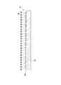
- FIG. 1 is a schematic plan view showing a touch panel provided with electrodes for a touch panel in the first embodiment.
- FIG. 2 is a cross-sectional view taken along line AA ′ of FIG.
- FIG. 3 is an enlarged plan view of a region surrounded by a dotted line D in FIG.
- the touch panel 10 of this embodiment includes a transparent base material (substrate) 20 and a touch panel electrode (electrode) 50 formed on an electrode forming surface 20a that is one surface of the transparent base material 20.
- the touch panel electrode 50 includes a plurality of strip-shaped electrodes 30 and a conductor (dummy region) 40 provided separately from the strip-shaped electrodes 30.
- a liquid crystal display panel (not shown) or the like is disposed under the transparent base (substrate) 20 (lower layer).
- the strip electrode 30 is formed so as to form a non-linear wavy line in which a plurality of refracting portions 31 are combined along the first direction (referred to as the Y direction in this embodiment) of the electrode forming surface 20a.
- a plurality of strip electrodes 30 formed in such wavy lines are arranged at a predetermined interval (predetermined pitch) along the second direction (referred to as the X direction in this embodiment) of the electrode forming surface 20a.
- predetermined pitch predetermined pitch
- the refracting portion 31 of the strip electrode 30 is a region refracted at an angle where the inner angle ⁇ is greater than 90 °, for example.
- the internal angle ⁇ of the refracting portion 31 may be about 120 ° to 150 °, for example, but is not particularly limited.
- the plurality of strip electrodes 30 are arranged so that the apex P of the refracting portion 31 is positioned on a line along the X direction.
- a large number of conductors (dummy regions) 40 are arranged apart from the strip electrode 30.
- Each conductor 40 is made of a conductive material formed in a strip shape.
- a large number of conductors 40 are arranged adjacent to the apex P of the refracting portion 31 of the strip electrode 30 so that the long sides extend in a direction inclined with respect to the X direction. That is, in the present embodiment, a large number of conductors 40 are arranged so that the long side is along the Y direction inclined 90 ° with respect to the X direction.
- the visual recognition of the virtual line Oi due to the illusion that occurs when observing the arrangement of the band-like band-like electrodes 30 is prevented. That is, when the band-shaped electrode 30 of the wavy line is arranged along the X direction, a virtual line Oi connecting the vertices P of the refracting portions 31 of the adjacent band-shaped electrodes 30 may be seen by an illusion. There is a possibility that the visibility of 10 may be lowered.
- the strip-shaped conductor 40 extending in the direction in which the long side is inclined with respect to the Y direction that is the extending direction of the virtual line Oi is disposed in the vicinity of the refracting portion 31 of the strip electrode 30.
- the virtual line Oi can be prevented from being visually recognized by an illusion.
- an image displayed on the touch panel 10 can be seen more clearly, and the visibility of the touch panel 10 can be improved.
- a plurality of conductors 40 are arranged apart from the strip electrode 30 to arrange the wavy strip electrodes 30.
- the conductor 40 is formed at all corresponding positions (near) of the refracting part 31, but the conductor 40 is formed only near a part of the refracting part 31. You can also.
- the conductor (dummy region) 40 is formed only in the vicinity of the refracting portion 31 of the band-shaped electrode 30 selected at random.
- the degree of formation of the conductor 40 can be, for example, the number thinned to such an extent that the virtual line Oi is prevented from being visually recognized.
- FIG. 4 is an enlarged plan view of a main part showing a touch panel provided with electrodes for the touch panel according to the second embodiment of the present invention.
- the touch panel 60 of the present embodiment includes a transparent substrate 20 and a touch panel electrode (electrode) 70 formed on the electrode forming surface (one surface) 20 a of the transparent substrate 20.
- the touch panel electrode 70 is composed of a plurality of strip electrodes 30 and a conductor (dummy region) 80 provided apart from the strip electrodes 30.
- the strip electrode 30 is formed so as to form a non-linear wavy line in which a plurality of refracting portions 31 are combined along the first direction (referred to as the Y direction in this embodiment) of the electrode forming surface 20a.
- a plurality of strip electrodes 30 formed in such wavy lines are arranged at a predetermined interval (predetermined pitch) along the second direction (referred to as the X direction in this embodiment) of the electrode forming surface 20a.
- predetermined pitch predetermined pitch
- a large number of conductors (dummy regions) 80 are arranged apart from the strip electrode 30.
- the conductor 80 of the present embodiment constitutes one (one) conductor 80 in which point-like conductive materials are arranged, for example, along the Y direction.
- a large number of conductors 80 in which such dotted conductive materials are arranged are arranged adjacent to the apex P of the refracting portion 31 of the strip electrode 30.
- the conductor 80 can be formed at a position corresponding to an arbitrary refracting portion 31 without forming the conductor 80 at a position corresponding to all the refracting portions 31.
- FIG. 5 is an enlarged plan view of a main part showing a touch panel provided with electrodes for the touch panel according to the third embodiment of the present invention.
- the touch panel 90 of the present embodiment includes a transparent substrate 20 and a touch panel electrode (electrode) 100 formed on an electrode formation surface (one surface) 20 a of the transparent substrate 20.
- the touch panel electrode 100 is composed of a plurality of strip electrodes 30 and a conductor (dummy region) 110 provided separately from the strip electrodes 30.
- the strip electrode 30 is formed so as to form a non-linear wavy line in which a plurality of refracting portions 31 are combined along the first direction (referred to as the Y direction in this embodiment) of the electrode forming surface 20a.
- the touch panel electrode 90 is formed by arranging a plurality of strip-shaped electrodes 30 formed in such wavy lines at predetermined intervals (predetermined pitch) along a second direction (referred to as X direction in the present embodiment) of the electrode forming surface 20a. Has been.
- a large number of conductors (dummy regions) 110 are arranged apart from the strip electrode 30.
- a large number of strip-shaped conductive materials are arranged adjacent to the apex P of the refracting portion 31 of the strip-shaped electrode 30.
- the individual conductors 110 are formed, for example, such that the long sides thereof are along one direction S1 and the other direction S2 constituting the refracting portion 31 of the strip electrode 30.
- the conductor 110 can be formed at a position corresponding to an arbitrary refracting portion 31 without forming the conductor 110 at a position corresponding to all the refracting portions 31.
- FIG. 6 is a main part enlarged plan view showing a touch panel provided with electrodes for a touch panel according to a fourth embodiment of the present invention.
- the touch panel 120 of this embodiment includes a transparent substrate 20 and a touch panel electrode (electrode) 130 formed on an electrode formation surface (one surface) 20 a of the transparent substrate 20.
- the touch panel electrode 130 is composed of a plurality of strip electrodes 30 and a conductor (dummy region) 140 provided separately from the strip electrodes 30.
- the strip electrode 30 is formed so as to form a non-linear wavy line in which a plurality of refracting portions 31 are combined along the first direction (referred to as the Y direction in this embodiment) of the electrode forming surface 20a.
- a plurality of strip-like electrodes 30 formed in such wavy lines are arranged at a predetermined interval (predetermined pitch) along the second direction (referred to as the X direction in this embodiment) of the electrode forming surface 20 a.
- predetermined pitch predetermined pitch
- a large number of conductors (dummy regions) 140 are arranged apart from the strip electrode 30.
- a large number of strip-shaped conductive materials are arranged adjacent to the apex P of the refracting portion 31 of the strip-shaped electrode 30.
- the individual conductors 140 are arranged so that the direction of the long side is inclined with respect to the X direction and the formation positions are random.
- the individual conductors 140 are arranged so that the formation positions are random.
- the individual conductors 140 may be formed so that the orientation (angle with respect to the X direction) of the individual conductors is random. it can. In this case, the formation position of the conductor 140, at least one of the directions of the conductor 140, or both can be made random.
- the size and shape of the conductor are not particularly limited, and can be any size and any shape.
- the conductor may be a dot shape, a triangle shape, a quadrangular shape, a pentagonal or more polygonal shape, a star shape, or the like.
- each conductor is not particularly limited as long as it is in the vicinity of the bent portion of the wavy band-shaped electrode, and at an arbitrary angle with respect to the second direction at an arbitrary position in the vicinity of the bent portion. It can be formed to extend in the inclined direction.
- an insulating layer is further formed so as to cover the strip electrode and the conductor formed on the electrode forming surface of the transparent substrate.
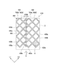
- FIG. 8 is a schematic plan view showing a touch panel provided with electrodes for a touch panel in the fifth embodiment.
- FIG. 9 is a cross-sectional view taken along the line AA ′ of FIG.
- FIG. 10 is an enlarged plan view of a region surrounded by a dotted line D in FIG.
- the touch panel 210 of the present embodiment includes a transparent base material (substrate) 220 and a touch panel electrode (electrode) 250 formed on an electrode forming surface 220a which is one surface of the transparent base material 220.
- the touch panel electrode 250 includes a pattern electrode formed by crossing a plurality of strip electrodes 230 and a conductor 240.
- a liquid crystal display panel (not shown) or the like is disposed under the transparent base material (substrate) 220 (lower layer).
- the strip electrode 230 is for a grid-shaped touch panel in which a plurality of strip electrodes 230a extending along the X direction in the drawing and a plurality of strip electrodes 230b extending along the Y direction in the drawing intersect at a predetermined angle.
- An electrode 250 is formed. That is, a grid-shaped touch panel electrode 250 is formed by providing a number of rectangular unit electrode patterns S connected in series.
- the crossing angle between the plurality of strip electrodes 230a extending along the X direction and the plurality of strip electrodes 230b extending along the Y direction is, for example, 90 °. That is, the strip electrode 230a and the strip electrode 230b are orthogonal to each other to constitute a touch panel electrode 250 having a mesh structure (mesh structure).
- the touch panel electrode 250 includes a first electrode pattern region E1 and a second electrode pattern region E2 arranged along a predetermined direction of the electrode formation surface 220a on the electrode formation surface 220a, and the first electrode pattern region E1 and the first electrode pattern region E1.
- a two-electrode pattern region E2 has a separation region E3 that is a separation region.
- the predetermined direction in which the first electrode pattern region E1 and the second electrode pattern region E2 are separated from each other is the X direction in the drawing.
- the separation region E3 is a region where the first electrode pattern region E1 and the second electrode pattern region E2 spread over a portion separated by a predetermined distance.
- the first electrode pattern region E1 and the second electrode pattern region E2 that are formed apart from each other are electrically separated from each other. That is, the strip electrode 230 in the first electrode pattern region E1 and the strip electrode 230 in the second electrode pattern region E2 are not connected to each other.
- the first electrode pattern region E1 and the second electrode pattern region E2 may be an electrode pattern to which a voltage is actually applied or a dummy electrode pattern.
- a large number of conductors (dummy regions) 240 are arranged in a separation region E3 provided between the first electrode pattern region E1 and the second electrode pattern region E2.
- Such a conductor 240 has a region extending at least in a predetermined direction of the electrode formation surface 220a, in this embodiment, an angle direction inclined with respect to the X direction, and is separated from the strip electrode 230. It is.
- the conductor 240 is formed in a rectangular parallelepiped shape extending in a direction inclined at an angle ⁇ with respect to the X direction, and the angle ⁇ is set to 45 °, for example.
- the first electrode pattern region E1 and the second electrode pattern region E2 extend in a direction inclined at an angle ⁇ with respect to the X direction to the separation region E3 that electrically separates the first electrode pattern region E1 and the second electrode pattern region E2.
- the conductor 240 it is possible to prevent the visibility of the separation region E3 where no electrode pattern exists from being lower than that of the peripheral portion. Thereby, an image displayed on the touch panel 210 can be seen more clearly, and the visibility of the touch panel 210 can be improved.
- the conductor 240 that improves the visibility of the separation region E3 is provided in a predetermined direction of the electrode forming surface 220a, that is, in the present embodiment, the first.
- the conductor 240 In order to avoid a short circuit when forming the first electrode pattern region E1 and the second electrode pattern region E2 by inclining with respect to the X direction which is the separation direction of the electrode pattern region E1 and the second electrode pattern region E2. Space can be secured. Thereby, even if the conductor 240 is formed in the separation region E3, it is possible to reliably prevent a short circuit between the first electrode pattern region E1 and the second electrode pattern region E2.
- FIG. 11 is a principal part enlarged plan view which shows the touchscreen provided with the electrode for touchscreens of 6th embodiment of this invention.
- the touch panel 260 of the present embodiment includes a transparent base material (substrate) 220 and a touch panel electrode (electrode) 70 formed on an electrode forming surface 220 a that is one surface of the transparent base material 220.
- the touch panel electrode 270 includes a pattern electrode formed by crossing a plurality of strip electrodes 280 and a conductor (dummy region) 290.
- the strip electrode 280 is a grid-shaped touch panel in which a plurality of strip electrodes 280a extending along the X direction in the drawing and a plurality of strip electrodes 280b extending along the Y direction intersect at a predetermined angle, for example, 90 °.
- the electrode 270 is formed.
- the electrode 270 for the touch panel is a first electrode pattern region E1 that is two electrode pattern regions spaced apart in a predetermined direction, for example, the X direction in the drawing, via the predetermined separation region E3 on the electrode formation surface 220a. And a second electrode pattern region E2.
- a large number of conductors 290 are arranged in a separation region E3 provided between the first electrode pattern region E1 and the second electrode pattern region E2.
- the conductor 290 of the present embodiment is a strip-shaped conductor that includes at least a region extending in an angle direction inclined with respect to the X direction, which is a predetermined direction of the electrode formation surface 220a, and is separated from the strip electrode 280. is there.
- the conductor 290 has a hook-like shape composed of a region extending along the Y direction, which is a direction inclined at an angle of 90 ° with respect to the X direction, and regions extending in the X direction from both ends of this region. It consists of the formed conductor.
- the separation region E3 that electrically separates the first electrode pattern region E1 and the second electrode pattern region E2 from each other includes a region extending in a direction inclined with respect to the X direction.
- the hook-shaped conductor (dummy region) 290 it is possible to prevent the visibility of the separation region E3 where no electrode pattern exists from being lower than the peripheral portion. Thereby, an image displayed on the touch panel 260 can be seen more clearly, and the visibility of the touch panel 260 can be improved.
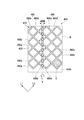
- FIG. 12 is an enlarged plan view of a main part showing a touch panel provided with electrodes for the touch panel according to the seventh embodiment of the present invention.
- the touch panel 300 of this embodiment includes a transparent base material (substrate) 320 and a touch panel electrode (electrode) 310 formed on an electrode forming surface 320a which is one surface of the transparent base material 320.
- the touch panel electrode 310 includes a pattern electrode formed by intersecting a plurality of strip electrodes 320 and a conductor (dummy region) 330.
- the strip electrode 320 includes a grid-shaped touch panel in which a plurality of strip electrodes 320a extending along the X direction in the drawing and a plurality of strip electrodes 320b extending along the Y direction intersect at a predetermined angle, for example, 90 °.
- a working electrode 310 is formed.
- the touch panel electrode 310 is a first electrode pattern region E1 which is two electrode pattern regions spaced apart in a predetermined direction, for example, the X direction in the figure, via a predetermined separation region E3 on the electrode formation surface 320a. And a second electrode pattern region E2.
- a large number of conductors (dummy regions) 330 are arranged in a separation region E3 provided between the first electrode pattern region E1 and the second electrode pattern region E2.
- the conductor 330 of the present embodiment is a point-like conductor arranged in an angle direction inclined with respect to the X direction which is a predetermined direction of the electrode forming surface 320a.
- one conductor 330 is composed of a set of three point-like conductors (dot-like conductor group).
- the touch panel 300 having such a configuration, the arrangement direction of a set of three point-like conductors in the separation region E3 that electrically separates the first electrode pattern region E1 and the second electrode pattern region E2 from each other.
- the conductors (dummy regions) 330 arranged in a direction inclined with respect to the X direction, it is possible to prevent the visibility of the separation region E3 where no electrode pattern exists from being lower than the peripheral portion thereof. . Thereby, an image displayed on the touch panel 300 can be seen more clearly, and the visibility of the touch panel 300 can be improved.
- the conductor may be composed of a mixture of strips and dots. Moreover, as long as the conductor includes at least a region extending in a direction inclined at an arbitrary angle with respect to a predetermined direction of the electrode formation surface, the other portions may be parallel to the predetermined direction.
- random means that a plurality of conductors are formed in random directions as long as the extending direction of the conductors is inclined with respect to a predetermined direction, or the formation positions in the separation region E3. Are formed at random positions without regularization.
- the conductor exists in the separation region E3, and the other part may be applied to the first electrode pattern region E1 and the second electrode pattern region E2.
- the shapes of the individual conductors do not have to be the same as each other, and conductors having different shapes can be randomly arranged.
- each unit electrode pattern has a diamond shape.
- an insulating layer is further formed so as to cover the strip electrode and the conductor formed on the electrode forming surface of the transparent substrate.
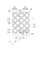
- FIG. 13 is a schematic plan view which shows the touchscreen provided with the electrode for touchscreens in 8th embodiment.
- FIG. 14 is a cross-sectional view taken along the line AA ′ of FIG.
- FIG. 15 is an enlarged plan view of a region surrounded by a dotted line D in FIG.
- the touch panel 410 of the present embodiment includes a transparent base material (substrate) 420 and a touch panel electrode (electrode) 450 formed on an electrode forming surface 420 a that is one surface of the transparent base material 420.
- the touch panel electrode 450 includes a pattern electrode formed by crossing a plurality of strip electrodes 430 with each other.
- a liquid crystal display panel (not shown) or the like is disposed under the transparent base material (substrate) 420 (lower layer).
- the strip electrode 430 includes a plurality of strip electrodes 430a extending along the first direction (referred to as L1 direction in the present embodiment) and a plurality of strip electrodes extending along the second direction (referred to as L2 direction in the present embodiment).
- 430b intersects at an angle ⁇ to form a grid-like touch panel electrode 450. That is, a grid-shaped touch panel electrode 450 is formed by providing a number of rectangular unit electrode patterns S connected in series.
- the angle ⁇ is, for example, 90 °
- the strip electrode 430a and the strip electrode 430b are orthogonal to each other to form a touch panel electrode 450 having a mesh structure (mesh structure). .
- the touch panel electrode 450 includes a first electrode pattern region E1 and a second electrode pattern region E2, which are two electrode pattern regions disposed adjacent to each other on the electrode formation surface 420a.
- the first electrode pattern region E1 and the second electrode pattern region E2 are electrically separated from each other. That is, the strip electrode 430 in the first electrode pattern region E1 and the strip electrode 430 in the second electrode pattern region E2 are not connected to each other.
- the first electrode pattern region E1 and the second electrode pattern region E2 may be an electrode pattern to which a voltage is actually applied or a dummy electrode pattern.
- an end portion 430e of the strip electrode 430 constituting the first electrode pattern region E1 and the second electrode pattern region E2 are formed on the side where the first electrode pattern region E1 and the second electrode pattern region E2 face each other (adjacent).
- the end portion 430e of the strip electrode 430 forms an overlapping portion (dummy region) 430W that overlaps with each other in the direction intersecting the first direction L1 and the second direction L2.
- the first electrode pattern region E1 and the second electrode pattern are indicated by an arrow V that intersects the first direction L1 and the second direction L2 and indicates the direction along the electrode formation surface 420a.
- the end portions 430e of the respective strip electrodes 430 form an overlapping portion 430W that overlaps each other.
- overlapping portions (dummy regions) 430W form a region including the end portion 430e of the strip electrode 430 formed integrally with the strip electrode 430. That is, the overlapping portion 430W is obtained by shifting the phases of the first electrode pattern region E1 and the second electrode pattern region E2 formed at the same pitch and approaching each other.
- the formation pitch of the strip electrodes 430 in the first electrode pattern region E1 and the second electrode pattern region E2 is the same, but the strip electrodes 430 in the first electrode pattern region E1 and the second electrode pattern region E2 are the same.
- the overlapping portion 430W can also be formed by changing the formation pitch of each other.
- the end portions 430e of the strip electrodes 430 are overlapped with the adjacent portions of the first electrode pattern region E1 and the second electrode pattern region E2 that are electrically separated from each other.
- the overlapping portion (dummy region) 430W By forming the overlapping portion (dummy region) 430W, the visibility of the adjacent portions between the electrode patterns can be prevented from being lower than that of the peripheral portions. Thereby, an image displayed on the touch panel 410 can be seen more clearly, and the visibility of the touch panel 410 can be improved.
- FIG. 16 is a principal part enlarged plan view which shows the touchscreen provided with the electrode for touchscreens of 9th embodiment of this invention.
- the touch panel 460 of the present embodiment includes a transparent base material (substrate) 420 and a touch panel electrode (electrode) 470 formed on an electrode forming surface 420 a that is one surface of the transparent base material 420.
- the touch panel electrode 470 includes a pattern electrode formed by crossing a plurality of strip electrodes 480.
- the strip-shaped electrode 480 includes a plurality of strip-shaped electrodes 480a extending along the first direction L1 and a plurality of strip-shaped electrodes 480b extending along the second direction L2 intersecting at an angle ⁇ , so that the grid-shaped touch panel electrode 470 is formed.
- a grid-shaped touch panel electrode 470 is formed by providing a number of rectangular unit electrode patterns S connected in series.
- the angle ⁇ is, for example, 90 °
- the strip electrode 480a and the strip electrode 480b are orthogonal to each other to constitute a touch panel electrode 470 having a mesh structure (mesh structure). .
- the touch panel electrode 470 includes a first electrode pattern region E1 and a second electrode pattern region E2, which are two electrode pattern regions disposed adjacent to each other on the electrode formation surface 420a.
- the first electrode pattern region E1 and the second electrode pattern region E2 are electrically separated from each other.
- an end portion 80e of the strip electrode 480 constituting the first electrode pattern region E1 and the second electrode pattern region E2 are formed on the side where the first electrode pattern region E1 and the second electrode pattern region E2 face each other (adjacent).
- the end portion 480e of the strip electrode 480 forms an overlapping portion (dummy region) 480W that overlaps with each other in the direction intersecting the first direction L1 and the second direction L2.
- the end portion 480e of the strip electrode 480 is formed in a dotted line shape in which dotted conductors are arranged along the first direction L1 and the second direction L2.
- the formation interval and size of the dotted conductors can be arbitrarily selected.
- the end portion 480e of the strip-shaped electrode 480 formed in a dotted line is formed in the adjacent portion between the first electrode pattern region E1 and the second electrode pattern region E2 that are electrically separated from each other.
- the overlapped portion (dummy region) 480W that is overlapped, the visibility of the adjacent portion between the electrode patterns can be prevented from being lower than that of the peripheral portion. Thereby, an image displayed on the touch panel 460 can be seen more clearly, and the visibility of the touch panel 460 can be improved.
- FIG. 17 is a principal part enlarged plan view which shows the touchscreen provided with the electrode for touchscreens of 10th Embodiment of this invention.
- the touch panel 590 of the present embodiment includes a transparent base material (substrate) 520 and a touch panel electrode (electrode) 500 formed on an electrode forming surface 520a which is one surface of the transparent base material 520.
- the touch panel electrode 500 is composed of a pattern electrode formed by crossing a plurality of strip electrodes 510 with each other.
- the strip-shaped electrode 510 includes a plurality of strip-shaped electrodes 510a extending along the first direction L1 and a plurality of strip-shaped electrodes 510b extending along the second direction L2 intersecting at an angle ⁇ to form a grid-shaped touch panel electrode 500.
- a grid-shaped touch panel electrode 500 is formed by providing a number of rectangular unit electrode patterns S connected in series.
- the angle ⁇ is, for example, 90 °
- the band-shaped electrode 510a and the band-shaped electrode 510b are orthogonal to each other to form a touch panel electrode 500 having a mesh structure (mesh structure). .
- the touch panel electrode 500 includes a first electrode pattern region E1 and a second electrode pattern region E2, which are two electrode pattern regions disposed adjacent to each other on the electrode formation surface 20a.
- the strip electrode 510 in the first electrode pattern region E1 and the strip electrode 510 in the second electrode pattern region E2 are electrically separated from each other.
- an end portion 510e of the strip-like electrode 510 constituting the first electrode pattern region E1 and the second electrode pattern region E2 are formed.
- An end portion 510e of the strip electrode 510 forms an overlapping portion (dummy region) 510W that overlaps with each other in the direction intersecting the first direction L1 and the second direction L2.
- the width of the end portion 510e of the strip electrode 510 constituting the overlapping portion (dummy region) 510W is smaller than that of the other portions. That is, the width G1 of the end portion 510e of the belt-like electrode 510 is formed to be half the size (half-width) of the width G2 in the region other than the overlapping portion (dummy region) 510W of the belt-like electrode 510. Note that the width G1 of the end portion 510e of the belt-like electrode 510 only needs to be smaller than the width G2 in a region other than the overlapping portion (dummy region) 510W of the belt-like electrode 510, and is not limited to a half width.
- the touch panel 590 having such a configuration, adjacent portions of the first electrode pattern region E1 and the second electrode pattern region E2 that are electrically separated from each other other than the overlapping portion (dummy region) 510W of the belt-like electrode 510 are provided.
- an overlapping portion (dummy region) 510W in which the end portions 510e of the strip-like electrode 510 formed to have a width G1 smaller than the width G2 in the region are overlapped, the visibility of the adjacent portions between the electrode patterns is improved in the peripheral portion. Can be prevented. Thereby, an image displayed on the touch panel 90 can be seen more clearly, and the visibility of the touch panel 90 can be improved.
- FIG. 18 is a main part enlarged plan view showing a touch panel including electrodes for a touch panel according to the eleventh embodiment of the present invention.
- the touch panel 520 of the present embodiment includes a transparent base material (substrate) 520 and a touch panel electrode (electrode) 530 formed on an electrode forming surface 520 a that is one surface of the transparent base material 520.
- the touch panel electrode 530 is composed of a pattern electrode formed by crossing a plurality of strip electrodes 540 with each other.
- the strip-shaped electrode 540 includes a plurality of strip-shaped electrodes 540a extending along the first direction L1 and a plurality of strip-shaped electrodes 540b extending along the second direction L2 intersecting at an angle ⁇ , so that the grid-shaped touch panel electrode 530 is formed.
- a grid-shaped touch panel electrode 530 is formed by providing a large number of rectangular unit electrode patterns S connected in series.
- the angle ⁇ is, for example, 90 °
- the strip electrode 540a and the strip electrode 540b are orthogonal to each other to constitute the touch panel electrode 130 having a mesh structure (mesh structure). .
- the touch panel electrode 530 includes a first electrode pattern region E1 and a second electrode pattern region E2, which are two electrode pattern regions disposed adjacent to each other on the electrode formation surface 520a.
- the strip electrode 540 in the first electrode pattern region E1 and the strip electrode 540 in the second electrode pattern region E2 are electrically separated from each other.
- an end portion 540e of the strip electrode 540 constituting the first electrode pattern region E1 and the second electrode pattern region E2 are formed on the side where the first electrode pattern region E1 and the second electrode pattern region E2 face each other (adjacent).
- the end portion 540e of the strip electrode 540 forms an overlapping portion (dummy region) 540W that overlaps with each other in the direction intersecting the first direction L1 and the second direction L2.
- the end portion 540e of the strip electrode 540 constituting the overlapping portion (dummy region) 540W of the first electrode pattern region E1 and the second electrode pattern region E2 is reduced in thickness as compared with other portions. Yes. That is, the thickness d1 of the end portion 540e of the strip electrode 540 is formed to be half of the thickness d2 in the region other than the overlapping portion 540W of the strip electrode 540.
- the thickness d1 of the end portion 540e of the strip electrode 540 only needs to be smaller than the thickness d2 in the region other than the overlapping portion 540W of the strip electrode 540, and is not limited to a half thickness.
- the thickness d2 in the region other than the overlapping portion 540W of the strip electrode 540 is adjacent to the first electrode pattern region E1 and the second electrode pattern region E2 that are electrically separated from each other.
- the overlapping portion 540W in which the end portions 540e of the strip electrode 540 formed to have a smaller thickness d1 are overlapped it is possible to prevent the visibility of the adjacent portions between the electrode patterns from being lower than the surrounding portions. . Accordingly, an image displayed on the touch panel 5120 can be seen more clearly, and the visibility of the touch panel 520 can be improved.
- the intersection angle between the strip electrode extending along the first direction and the strip electrode extending along the second direction is an arbitrary angle other than a right angle. Can be crossed at. When the crossing angle is other than 90 °, each unit electrode pattern has a diamond shape.
- an insulating layer is further formed so as to cover the strip electrode and the conductor formed on the electrode forming surface of the transparent substrate.
- the transparent substrate examples include polyethylene terephthalate (PET), polycarbonate (PC), polymethyl methacrylate (PMMA), polyethylene naphthalate (PEN), polyether sulfone (PES), cyclic olefin copolymer (COC), triacetyl Cellulose (Triacetylcellulose; TAC) film, Polyvinyl alcohol (PVA) film, Polyimide (PI) film, Polystyrene (PS), Biaxially oriented polystyrene (K resin-containing biaxially oriented PS, BOPS) or BOPS Examples thereof include a base material made of tempered glass. Moreover, in order to improve the adhesive force between the transparent substrate and the touch panel electrode 50, the transparent substrate may be subjected to a high-frequency treatment or a primer treatment.
- the strip electrode and the conductor are made of, for example, conductive ink used for forming a conductive circuit.
- conductive ink for example, polymer type conductive ink, silver ink composition, commercially available metal paste, metal nano ink, metal complex ink, and the like are used.
- the conductive ink it is preferable to use an ink containing metal particles having a particle diameter smaller than the width and thickness of the strip electrode and the size and thickness of the conductor.
- the conductor 40 is not concerned with the resistance value of the electrode for touch panels, you may form using the ink from which resistance value becomes high.
- the strip electrode and the conductor are not limited to the formation using the conductive ink.
- a known method for forming a conductor such as formation of a conductor by etching, formation of a conductor by vapor deposition of a conductive material, or formation of a conductor by sputtering can be employed.
- polymer-type conductive ink examples include those in which conductive fine particles such as silver powder, gold powder, platinum powder, aluminum powder, palladium powder, rhodium powder, carbon powder (carbon black, carbon nanotube, etc.) are blended in the resin composition Is mentioned.
- the polymer type conductive ink becomes a thermosetting type capable of forming a coating film forming a conductive circuit at 200 ° C. or less, for example, about 100 to 150 ° C.
- thermosetting type known types such as a photocurable type, a permeation drying type, and a solvent volatile type are used.
- the photocurable polymer type conductive ink contains a photocurable resin in the resin composition and has a short curing time, so that the production efficiency can be improved.
- the photocurable polymer type conductive ink include, for example, a thermoplastic resin alone or a blend resin composition of a thermoplastic resin and a crosslinkable resin (particularly, a crosslinkable resin composed of polyester and isocyanate, etc.) and 60 mass of conductive fine particles.
- % Or more and 10% by mass or more of a polyester resin that is, a solvent volatile type or a crosslinked / thermoplastic combined type (however, the thermoplastic type is 50% by mass or more), or a thermoplastic resin Or a blended resin composition of a thermoplastic resin and a crosslinkable resin (especially a crosslinkable resin composed of polyester and isocyanate, etc.) containing 10% by mass or more of a polyester resin, that is, a crosslinkable type or a crosslinked / thermal A plastic combination type is preferably used.
- the silver ink composition for example, a composition in which a metal silver forming material described later is blended is used.
- the conductive circuit is formed by solidifying the silver ink composition deposited on the electrode forming surface of the transparent substrate. The solidification treatment is performed by heating (baking) the silver ink composition deposited on the electrode forming surface of the transparent substrate as will be described later.
- the content of silver derived from the metal silver forming material is preferably 5% by mass or more, and more preferably 10% by mass or more. By being in such a range, the conductive circuit formed by the method to be described later is more excellent in quality.
- the upper limit of the silver content is not particularly limited as long as the effects of the present embodiment are not impaired, but it is preferably 25% by mass in consideration of handling properties and the like.
- silver derived from a metallic silver forming material means silver in the metallic silver forming material blended during the production of the silver ink composition, unless otherwise specified. The concept includes both silver that subsequently constitutes a metal silver forming material, and silver and silver itself in a decomposition product produced by decomposition of the metal silver forming material after blending.
- the metallic silver forming material is decomposed by heating or the like to form metallic silver.
- the metallic silver forming material may be used alone or in combination of two or more. When using 2 or more types together, the combination and ratio can be adjusted arbitrarily.
- silver carboxylate examples include silver carboxylate having a group represented by the formula “—COOAg”.
- the silver carboxylate is not particularly limited as long as it has a group represented by the formula “—COOAg”.
- the number of groups represented by the formula “—COOAg” may be one, or two or more.
- the position of the group represented by the formula “—COOAg” in the silver carboxylate is not particularly limited.
- the silver carboxylate is represented by the following general formula (1): ⁇ -ketocarboxylate silver (hereinafter sometimes abbreviated as “ ⁇ -ketocarboxylate (1)”) and the following general formula (2). It is preferable that it is 1 or more types selected from the group which consists of silver carboxylate (henceforth abbreviated as “silver carboxylate (2)").
- the term “silver carboxylate” is not limited to “silver ⁇ -ketocarboxylate (1)” and “silver silver carboxylate (2)”, unless otherwise specified. It is intended to mean “silver carboxylate having a group represented by the formula“ —COOAg ””.
- R represents an aliphatic hydrocarbon group having 1 to 20 carbon atoms in which one or more hydrogen atoms may be substituted with a substituent, a phenyl group, a hydroxyl group, an amino group, or a group represented by the general formula “R 1 -CY 2- ",” CY 3- “,” R 1 -CHY- “,” R 2 O- “,” R 5 R 4 N- “,” (R 3 O) 2 CY- “or” R 6 -C ( ⁇ O) —CY 2 — ”;
- Y is independently a fluorine atom, a chlorine atom, a bromine atom or a hydrogen atom;
- R 1 is an aliphatic hydrocarbon group or phenyl group having 1 to 19 carbon atoms;
- R 2 is an aliphatic group having 1 to 20 carbon atoms
- R 3 is an aliphatic hydrocarbon group having 1 to 16 carbon atoms;
- R 4 and R 5 are each independently an aliphatic hydrocarbon group having 1
- R 8 is an aliphatic hydrocarbon group having 1 to 19 carbon atoms, a carboxy group, or a group represented by the formula “—C ( ⁇ O) —OAg”, wherein the aliphatic hydrocarbon group is a methylene group. And one or more of the methylene groups may be substituted with a carbonyl group.
- the silver ⁇ -ketocarboxylate (1) is represented by the general formula (1).
- R is an aliphatic hydrocarbon group having 1 to 20 carbon atoms in which one or more hydrogen atoms may be substituted with a substituent, a phenyl group, a hydroxyl group, an amino group, or a group represented by the general formula “R 1 -CY 2 “-”, “CY 3 —”, “R 1 —CHY—”, “R 2 O—”, “R 5 R 4 N—”, “(R 3 O) 2 CY—” or “R 6 —C ( ⁇ O) —CY 2 — ”.
- the aliphatic hydrocarbon group having 1 to 20 carbon atoms in R may be any of linear, branched and cyclic (aliphatic cyclic group), and when it is cyclic, it may be monocyclic or polycyclic .
- the aliphatic hydrocarbon group may be either a saturated aliphatic hydrocarbon group or an unsaturated aliphatic hydrocarbon group.
- the aliphatic hydrocarbon group preferably has 1 to 10 carbon atoms, and more preferably 1 to 6 carbon atoms.
- Preferred examples of the aliphatic hydrocarbon group for R include an alkyl group, an alkenyl group, and an alkynyl group.
- Examples of the linear or branched alkyl group in R include a methyl group, ethyl group, n-propyl group, isopropyl group, n-butyl group, isobutyl group, sec-butyl group, tert-butyl group, n -Pentyl group, isopentyl group, neopentyl group, tert-pentyl group, 1-methylbutyl group, 2-methylbutyl group, n-hexyl group, 1-methylpentyl group, 2-methylpentyl group, 3-methylpentyl group, 4- Methylpentyl group, 1,1-dimethylbutyl group, 2,2-dimethylbutyl group, 3,3-dimethylbutyl group, 2,3-dimethylbutyl group, 1-ethylbutyl group, 2-ethylbutyl group, 3-ethylbutyl group 1-ethyl-1-methylpropyl group,
- Examples of the cyclic alkyl group in R include cyclopropyl group, cyclobutyl group, cyclopentyl group, cyclohexyl group, cycloheptyl group, cyclooctyl group, cyclononyl group, cyclodecyl group, norbornyl group, isobornyl group, 1-adamantyl group, 2- Examples thereof include an adamantyl group and a tricyclodecyl group.
- alkenyl group in R examples include a vinyl group (ethenyl group, —CH ⁇ CH 2 ), an allyl group (2-propenyl group, —CH 2 —CH ⁇ CH 2 ), and a 1-propenyl group (—CH ⁇ CH—CH).
- one single bond (C—C) between carbon atoms of the alkyl group in R such as ethynyl group (—C ⁇ CH), propargyl group (—CH 2 —C ⁇ CH), etc. ) Is a group in which a triple bond (C ⁇ C) is substituted.
- one or more hydrogen atoms may be substituted with a substituent, and preferred examples of the substituent include a fluorine atom, a chlorine atom, and a bromine atom.
- the number and position of substituents are not particularly limited. When the number of substituents is plural, the plural substituents may be the same as or different from each other. That is, all the substituents may be the same, all the substituents may be different, or only some of the substituents may be different.
- the phenyl group in R may have one or more hydrogen atoms substituted with a substituent, and the preferred substituent is a saturated or unsaturated monovalent aliphatic hydrocarbon group having 1 to 16 carbon atoms.
- a monovalent group formed by bonding the aliphatic hydrocarbon group to an oxygen atom, a fluorine atom, a chlorine atom, a bromine atom, a hydroxyl group (—OH), a cyano group (—C ⁇ N), a phenoxy group (—O—), C 6 H 5 ) and the like can be exemplified, and the number and position of substituents are not particularly limited. When the number of substituents is plural, the plural substituents may be the same as or different from each other. Examples of the aliphatic hydrocarbon group as a substituent include the same aliphatic hydrocarbon groups as those described above for R except that the number of carbon atoms is 1 to 16.
- Y in R each independently represents a fluorine atom, a chlorine atom, a bromine atom or a hydrogen atom.
- a plurality of Y may be the same or different from each other. Good.
- R 1 in R is an aliphatic hydrocarbon group having 1 to 19 carbon atoms or a phenyl group (C 6 H 5 —), and the aliphatic hydrocarbon group in R 1 has 1 to 19 carbon atoms. Except for this point, the same aliphatic hydrocarbon groups as those in R can be exemplified.
- R 2 in R is an aliphatic hydrocarbon group having 1 to 20 carbon atoms, and examples thereof are the same as the aliphatic hydrocarbon group in R.
- R 3 in R is an aliphatic hydrocarbon group having 1 to 16 carbon atoms, and examples thereof are the same as the aliphatic hydrocarbon group in R except that the carbon number is 1 to 16.
- R 4 and R 5 in R are each independently an aliphatic hydrocarbon group having 1 to 18 carbon atoms. That is, R 4 and R 5 may be the same as or different from each other, and examples thereof are the same as the aliphatic hydrocarbon group for R except that the number of carbon atoms is 1 to 18.
- R 6 in R is an aliphatic hydrocarbon group having 1 to 19 carbon atoms, a hydroxyl group or a group represented by the formula “AgO—”, and the aliphatic hydrocarbon group in R 6 has 1 to Except for being 19, it is possible to exemplify the same as the aliphatic hydrocarbon group for R.
- R is preferably a linear or branched alkyl group, a group represented by the general formula “R 6 —C ( ⁇ O) —CY 2 —”, a hydroxyl group or a phenyl group.
- R 6 is preferably a linear or branched alkyl group, a hydroxyl group, or a group represented by the formula “AgO—”.
- each X is independently a hydrogen atom, an aliphatic hydrocarbon group having 1 to 20 carbon atoms, a halogen atom, a phenyl group in which one or more hydrogen atoms may be substituted with a substituent, or benzyl Group (C 6 H 5 —CH 2 —), cyano group, N-phthaloyl-3-aminopropyl group, 2-ethoxyvinyl group (C 2 H 5 —O—CH ⁇ CH—), or a group represented by the general formula “R 7 It is a group represented by “O—”, “R 7 S—”, “R 7 —C ( ⁇ O) —” or “R 7 —C ( ⁇ O) —O—”.
- Examples of the aliphatic hydrocarbon group having 1 to 20 carbon atoms in X are the same as the aliphatic hydrocarbon group in R.
- halogen atom in X examples include a fluorine atom, a chlorine atom, a bromine atom, and an iodine atom.
- the substituent include a halogen atom (fluorine atom, chlorine atom, bromine atom, iodine atom), nitro A group (—NO 2 ) and the like can be exemplified, and the number and position of substituents are not particularly limited. When the number of substituents is plural, the plural substituents may be the same as or different from each other.
- R 7 in X represents an aliphatic hydrocarbon group having 1 to 10 carbon atoms, a thienyl group (C 4 H 3 S—), or a phenyl group or diphenyl in which one or more hydrogen atoms may be substituted with a substituent. group (biphenyl group, C 6 H 5 -C 6 H 4 -) it is.
- Examples of the aliphatic hydrocarbon group for R 7 include those similar to the aliphatic hydrocarbon group for R except that the aliphatic hydrocarbon group has 1 to 10 carbon atoms.
- examples of the substituent of the phenyl group and a diphenyl group in R 7, halogen atom (fluorine atom, chlorine atom, bromine atom, iodine atom) can be exemplified the like, the number and position of the substituent is not particularly limited. When the number of substituents is plural, the plural substituents may be the same as or different from each other.
- R 7 is a thienyl group or a diphenyl group
- the bonding position of these with an adjacent group or atom (oxygen atom, sulfur atom, carbonyl group, carbonyloxy group) in X is not particularly limited.
- the thienyl group may be either a 2-thienyl group or a 3-thienyl group.
- two Xs may be bonded as one group through a double bond with a carbon atom sandwiched between two carbonyl groups.
- a group represented by “ ⁇ CH—C 6 H 4 —NO 2 ” can be exemplified.
- X is preferably a hydrogen atom, a linear or branched alkyl group, or a benzyl group, and at least one X is preferably a hydrogen atom.
- the silver ⁇ -ketocarboxylate (1) is silver 2-methylacetoacetate (CH 3 —C ( ⁇ O) —CH (CH 3 ) —C ( ⁇ O) —OAg), silver acetoacetate (CH 3 —C ( ⁇ O) —CH 2 —C ( ⁇ O) —OAg), silver 2-ethylacetoacetate (CH 3 —C ( ⁇ O) —CH (CH 2 CH 3 ) —C ( ⁇ O) —OAg), propionylacetic acid Silver (CH 3 CH 2 —C ( ⁇ O) —CH 2 —C ( ⁇ O) —OAg), silver 2-n-butylacetoacetate (CH 3 —C ( ⁇ O) —CH (CH 2 CH 2 CH 2 CH 3 ) —C ( ⁇ O) —OAg), silver 2-benzylacetoacetate (CH 3 —C ( ⁇ O) —CH (CH 2 C 6 H 5 ) —C ( ⁇ O) —OAg), benzoylacetic acid Silver
- ⁇ -ketocarboxylate (1) can further reduce the concentration of the remaining raw materials and impurities in the conductor (metal silver) formed by post-treatment such as drying treatment or heating (firing) treatment.
- post-treatment such as drying treatment or heating (firing) treatment.
- the ⁇ -ketocarboxylate (1) is decomposed at a low temperature of preferably 60 ° C. to 210 ° C., more preferably 60 ° C. to 200 ° C., without using a reducing agent known in the art as described later.
- metallic silver can be formed. And by using together with a reducing agent, it decomposes at a lower temperature to form metallic silver.
- ⁇ -ketocarboxylate (1) may be used alone or in combination of two or more.
- the combination and ratio can be adjusted arbitrarily.
- the silver carboxylate (2) is represented by the general formula (2).
- R 8 is an aliphatic hydrocarbon group having 1 to 19 carbon atoms, a carboxy group (—COOH), or a group represented by the formula “—C ( ⁇ O) —OAg”.
- Examples of the aliphatic hydrocarbon group for R 8 include those similar to the aliphatic hydrocarbon group for R except that the aliphatic hydrocarbon group has 1 to 19 carbon atoms. However, the aliphatic hydrocarbon group for R 8 preferably has 1 to 15 carbon atoms, and more preferably 1 to 10 carbon atoms.
- the aliphatic hydrocarbon group for R 8 has a methylene group (—CH 2 —)
- one or more of the methylene groups may be substituted with a carbonyl group.
- the number and position of the methylene group which may be substituted with a carbonyl group are not particularly limited, and all methylene groups may be substituted with a carbonyl group.
- the “methylene group” is not only a single group represented by the formula “—CH 2 —” but also one of alkylene groups in which a plurality of groups represented by the formula “—CH 2 —” are linked. And a group represented by the formula “—CH 2 —”.
- Silver carboxylate (2) includes silver pyruvate (CH 3 —C ( ⁇ O) —C ( ⁇ O) —OAg), silver acetate (CH 3 —C ( ⁇ O) —OAg), silver butyrate (CH 3 — (CH 2 ) 2 —C ( ⁇ O) —OAg), silver isobutyrate ((CH 3 ) 2 CH—C ( ⁇ O) —OAg), silver 2-ethylhexanoate (CH 3 — (CH 2 ) 3 —CH (CH 2 CH 3 ) —C ( ⁇ O) —OAg), silver neodecanoate (CH 3 — (CH 2 ) 5 —C (CH 3 ) 2 —C ( ⁇ O) —OAg), Shu Silver oxide (AgO—C ( ⁇ O) —C ( ⁇ O) —OAg) or silver malonate (AgO—C ( ⁇ O) —CH 2 —C ( ⁇ O) —OAg) is preferable.
- silver oxalate (AgO—C ( ⁇ O) —C ( ⁇ O) —OAg) and silver malonate (AgO—C ( ⁇ O) —CH 2 —C ( ⁇ O) —OAg)
- silver oxalate (AgO—C ( ⁇ O) —C ( ⁇ O) —OAg)
- silver malonate (AgO—C ( ⁇ O) —CH 2 —C ( ⁇ O) —OAg)
- —COOAg one of the groups represented by the formula “—COOH” (HO—C ( ⁇ O) —C ( ⁇ O) —OAg, HO)
- —C ( ⁇ O) —CH 2 —C ( ⁇ O) —OAg is —COOH
- silver carboxylate (2) is also used in the conductor (metal silver) formed by post-treatment such as drying or heating (firing) treatment.
- concentration can be further reduced.
- a reducing agent it decomposes at a lower temperature to form metallic silver.
- silver carboxylate (2) may be used alone or in combination of two or more.
- the combination and ratio can be adjusted arbitrarily.
- the silver ink composition in particular, when the metal silver forming material is the silver carboxylate, in addition to the metal silver forming material, an amine compound having a carbon number of 25 or less, a quaternary ammonium salt, ammonia, and the above
- an amine compound having a carbon number of 25 or less in addition to the metal silver forming material, an amine compound having a carbon number of 25 or less, a quaternary ammonium salt, ammonia, and the above
- One or more nitrogen-containing compounds selected from the group consisting of ammonium salts formed by reaction of amine compounds or ammonia with acids hereinafter sometimes simply referred to as “nitrogen-containing compounds”.
- an amine compound having 25 or less carbon atoms is referred to as “amine compound”
- a quaternary ammonium salt having 25 or less carbon atoms is referred to as “quaternary ammonium salt”
- an ammonium salt obtained by reacting an amine compound having 25 or less carbon atoms with an acid Is sometimes abbreviated as “ammonium salt derived from an amine compound”, and an ammonium salt formed by reacting ammonia with an acid is sometimes abbreviated as “ammonium salt derived from ammonia”.
- the amine compound has 1 to 25 carbon atoms, and may be any of primary amine, secondary amine, and tertiary amine.
- the quaternary ammonium salt has 4 to 25 carbon atoms.
- the amine compound and the quaternary ammonium salt may be either chain or cyclic. Further, the number of nitrogen atoms constituting the amine moiety or ammonium salt moiety (for example, the nitrogen atom constituting the amino group (—NH 2 ) of the primary amine) may be 1 or 2 or more.
- Examples of the primary amine include monoalkylamines, monoarylamines, mono (heteroaryl) amines, and diamines in which one or more hydrogen atoms may be substituted with a substituent.
- the alkyl group constituting the monoalkylamine may be linear, branched or cyclic, and examples thereof are the same as the alkyl group in R, and are linear or branched having 1 to 19 carbon atoms. It is preferably a chain alkyl group or a cyclic alkyl group having 3 to 7 carbon atoms.
- preferable monoalkylamine examples include n-butylamine, n-hexylamine, n-octylamine, n-dodecylamine, n-octadecylamine, sec-butylamine, tert-butylamine, 3-aminopentane, 3 Examples include -methylbutylamine, 2-aminooctane, 2-ethylhexylamine, and 1,2-dimethyl-n-propylamine.
- aryl group constituting the monoarylamine examples include a phenyl group, a 1-naphthyl group, a 2-naphthyl group and the like, and preferably has 6 to 10 carbon atoms.
- the heteroaryl group constituting the mono (heteroaryl) amine has a heteroatom as an atom constituting the aromatic ring skeleton, and the heteroatom includes a nitrogen atom, a sulfur atom, an oxygen atom, and a boron atom. Can be illustrated.
- the number of the said hetero atom which comprises an aromatic ring skeleton is not specifically limited, One may be sufficient and two or more may be sufficient. When there are two or more, these heteroatoms may be the same or different from each other. That is, these heteroatoms may all be the same, may all be different, or may be partially different.
- the heteroaryl group may be monocyclic or polycyclic, and the number of ring members (the number of atoms constituting the ring skeleton) is not particularly limited, but is preferably a 3- to 12-membered ring.
- Examples of the monoaryl group having 1 to 4 nitrogen atoms as the heteroaryl group include pyrrolyl group, pyrrolinyl group, imidazolyl group, pyrazolyl group, pyridyl group, pyrimidyl group, pyrazinyl group, pyridazinyl group, triazolyl group, tetrazolyl group A pyrrolidinyl group, an imidazolidinyl group, a piperidinyl group, a pyrazolidinyl group, and a piperazinyl group, preferably a 3- to 8-membered ring, and more preferably a 5- to 6-membered ring.
- Examples of the monoaryl group having one oxygen atom as the heteroaryl group include a furanyl group, preferably a 3- to 8-membered ring, and more preferably a 5- to 6-membered ring.
- Examples of the monoaryl group having one sulfur atom as the heteroaryl group include a thienyl group, preferably a 3- to 8-membered ring, and more preferably a 5- to 6-membered ring.
- Examples of the monoaryl group having 1 to 2 oxygen atoms and 1 to 3 nitrogen atoms as the heteroaryl group include an oxazolyl group, an isoxazolyl group, an oxadiazolyl group, and a morpholinyl group.
- it is a 5- to 6-membered ring.
- the monoaryl group having 1 to 2 sulfur atoms and 1 to 3 nitrogen atoms as the heteroaryl group include a thiazolyl group, a thiadiazolyl group, and a thiazolidinyl group, and is a 3- to 8-membered ring.
- a 5- to 6-membered ring is preferable.
- Examples of the polyaryl having 1 to 5 nitrogen atoms as the heteroaryl group include indolyl group, isoindolyl group, indolizinyl group, benzimidazolyl group, quinolyl group, isoquinolyl group, indazolyl group, benzotriazolyl group, tetra Examples include a zolopyridyl group, a tetrazolopyridazinyl group, and a dihydrotriazolopyridazinyl group, preferably a 7-12 membered ring, and more preferably a 9-10 membered ring.
- Examples of the polyaryl group having 1 to 3 sulfur atoms as the heteroaryl group include a dithiaphthalenyl group and a benzothiophenyl group, preferably a 7 to 12 membered ring, preferably a 9 to 10 membered ring. More preferably, it is a ring.
- Examples of the polyaryl group having 1 to 2 oxygen atoms and 1 to 3 nitrogen atoms as the heteroaryl group include benzoxazolyl and benzooxadiazolyl groups. Preferably, it is a 9 to 10 membered ring.
- Examples of the polyaryl group having 1 to 2 sulfur atoms and 1 to 3 nitrogen atoms as the heteroaryl group include a benzothiazolyl group and a benzothiadiazolyl group, and is a 7 to 12 membered ring. Preferably, it is a 9 to 10 membered ring.
- the diamine only needs to have two amino groups, and the positional relationship between the two amino groups is not particularly limited.
- the preferred diamine in the monoalkylamine, monoarylamine or mono (heteroaryl) amine, one hydrogen atom other than the hydrogen atom constituting the amino group (—NH 2 ) is substituted with an amino group.
- the diamine preferably has 1 to 10 carbon atoms, and more preferable examples include ethylenediamine, 1,3-diaminopropane, and 1,4-diaminobutane.
- secondary amine examples include dialkylamine, diarylamine, di (heteroaryl) amine and the like in which one or more hydrogen atoms may be substituted with a substituent.
- the alkyl group constituting the dialkylamine is the same as the alkyl group constituting the monoalkylamine, and is a linear or branched alkyl group having 1 to 9 carbon atoms, or having 3 to 7 carbon atoms.
- a cyclic alkyl group is preferred.
- Two alkyl groups in one molecule of dialkylamine may be the same or different from each other.
- Specific examples of preferable dialkylamine include N-methyl-n-hexylamine, diisobutylamine, and di (2-ethylhexyl) amine.
- the aryl group constituting the diarylamine is the same as the aryl group constituting the monoarylamine, and preferably has 6 to 10 carbon atoms. Two aryl groups in one molecule of diarylamine may be the same as or different from each other.
- the heteroaryl group constituting the di (heteroaryl) amine is the same as the heteroaryl group constituting the mono (heteroaryl) amine, and is preferably a 6-12 membered ring.
- Two heteroaryl groups in one molecule of di (heteroaryl) amine may be the same as or different from each other.
- tertiary amine examples include trialkylamine and dialkylmonoarylamine in which one or more hydrogen atoms may be substituted with a substituent.
- the alkyl group constituting the trialkylamine is the same as the alkyl group constituting the monoalkylamine, and is a linear or branched alkyl group having 1 to 19 carbon atoms, or 3 to 7 carbon atoms.
- the cyclic alkyl group is preferably.
- the three alkyl groups in one molecule of trialkylamine may be the same as or different from each other. That is, all three alkyl groups may be the same, all may be different, or only a part may be different.
- Specific examples of preferable trialkylamine include N, N-dimethyl-n-octadecylamine and N, N-dimethylcyclohexylamine.
- the alkyl group constituting the dialkyl monoarylamine is the same as the alkyl group constituting the monoalkylamine, and is a linear or branched alkyl group having 1 to 6 carbon atoms, or 3 to 3 carbon atoms. 7 is a cyclic alkyl group. Two alkyl groups in one molecule of dialkyl monoarylamine may be the same or different from each other.
- the aryl group constituting the dialkyl monoarylamine is the same as the aryl group constituting the monoarylamine, and preferably has 6 to 10 carbon atoms.
- examples of the quaternary ammonium salt include halogenated tetraalkylammonium, in which one or more hydrogen atoms may be substituted with a substituent.
- the alkyl group constituting the halogenated tetraalkylammonium is the same as the alkyl group constituting the monoalkylamine, and preferably has 1 to 19 carbon atoms.
- the four alkyl groups in one molecule of the halogenated tetraalkylammonium may be the same or different from each other. That is, all four alkyl groups may be the same, all may be different, or only a part may be different.
- halogen constituting the halogenated tetraalkylammonium examples include fluorine, chlorine, bromine and iodine.
- Specific examples of preferred tetraalkylammonium halides include dodecyltrimethylammonium bromide.
- the chain amine compound and the quaternary organic ammonium salt have been mainly described.
- the nitrogen atom constituting the amine moiety or the ammonium salt moiety has a ring skeleton structure ( A heterocyclic compound which is a part of a heterocyclic skeleton structure) may be used. That is, the amine compound may be a cyclic amine, and the quaternary ammonium salt may be a cyclic ammonium salt.
- the ring (ring containing the nitrogen atom constituting the amine moiety or ammonium salt moiety) structure may be monocyclic or polycyclic, and the number of ring members (number of atoms constituting the ring skeleton) is also particularly limited. Any of an aliphatic ring and an aromatic ring may be sufficient. If it is a cyclic amine, a pyridine can be illustrated as a preferable thing.
- the “hydrogen atom optionally substituted with a substituent” means a nitrogen atom constituting an amine moiety or an ammonium salt moiety.
- the number of substituents at this time is not particularly limited, and may be one or two or more, and all of the hydrogen atoms may be substituted with substituents. When the number of substituents is plural, the plural substituents may be the same as or different from each other. That is, the plurality of substituents may all be the same, may all be different, or only some may be different. Further, the position of the substituent is not particularly limited.
- Examples of the substituent in the amine compound and the quaternary ammonium salt include an alkyl group, an aryl group, a halogen atom, a cyano group, a nitro group, a hydroxyl group, and a trifluoromethyl group (—CF 3 ).
- examples of the halogen atom include a fluorine atom, a chlorine atom, a bromine atom, and an iodine atom.
- the alkyl group constituting the monoalkylamine has a substituent
- the alkyl group has an aryl group as a substituent, a linear or branched alkyl group having 1 to 9 carbon atoms, or a substituent.
- a cyclic alkyl group having 3 to 7 carbon atoms having an alkyl group having 1 to 5 carbon atoms is preferable, and a monoalkylamine having such a substituent is specifically 2-phenylethylamine. , Benzylamine, and 2,3-dimethylcyclohexylamine.
- aryl group and the alkyl group which are substituents may further have one or more hydrogen atoms substituted with halogen atoms, and as monoalkylamines having such substituents substituted with halogen atoms, 2-bromobenzylamine.
- halogen atom include a fluorine atom, a chlorine atom, a bromine atom, and an iodine atom.
- the aryl group constituting the monoarylamine has a substituent
- the aryl group is preferably an aryl group having 6 to 10 carbon atoms having a halogen atom as the substituent, and the monoaryl having such a substituent
- Specific examples of the amine include bromophenylamine.
- examples of the halogen atom include a fluorine atom, a chlorine atom, a bromine atom, and an iodine atom.
- the alkyl group constituting the dialkylamine has a substituent
- the alkyl group is preferably a linear or branched alkyl group having 1 to 9 carbon atoms and having a hydroxyl group or an aryl group as a substituent.
- Specific examples of the dialkylamine having such a substituent include diethanolamine and N-methylbenzylamine.
- the amine compound is n-propylamine, n-butylamine, n-hexylamine, n-octylamine, n-dodecylamine, n-octadecylamine, sec-butylamine, tert-butylamine, 3-aminopentane, 3-methyl.
- the amine compound has a branched alkyl group. Those are preferred.
- ammonium salts derived from amine compounds is an ammonium salt obtained by reacting the amine compound with an acid
- the acid may be an inorganic acid such as hydrochloric acid, sulfuric acid, or nitric acid, or an organic acid such as acetic acid.
- An acid may be used, and the type of acid is not particularly limited.
- ammonium salt derived from the amine compound examples include, but are not limited to, n-propylamine hydrochloride, N-methyl-n-hexylamine hydrochloride, N, N-dimethyl-n-octadecylamine hydrochloride and the like. .
- ammonia-derived ammonium salt is an ammonium salt obtained by reacting ammonia with an acid, and the acid may be the same as that of the ammonium salt derived from the amine compound.
- the ammonium salt derived from ammonia include ammonium chloride, but are not limited thereto.
- the amine compound, the quaternary ammonium salt, the ammonium salt derived from the amine compound, and the ammonium salt derived from ammonia may be used alone or in combination of two or more. Also good. When using 2 or more types together, the combination and ratio can be adjusted arbitrarily.
- nitrogen-containing compound you may use individually 1 type selected from the group which consists of said amine compound, quaternary ammonium salt, ammonium salt derived from amine compound, and ammonium salt derived from ammonia, Two or more kinds may be used in combination. When using 2 or more types together, the combination and ratio can be adjusted arbitrarily.
- the compounding amount of the nitrogen-containing compound is preferably 0.4 to 15 mol, more preferably 0.8 to 5 mol, per mol of the silver carboxylate.
- the silver ink composition is further improved in stability and the quality of the conductive circuit is further improved. Furthermore, a conductive circuit can be formed more stably without performing heat treatment at a high temperature.
- the silver ink composition may further contain a reducing agent in addition to the metallic silver forming material.
- a reducing agent By blending a reducing agent, the silver ink composition can more easily form metallic silver.
- metallic silver (conductor) having sufficient conductivity can be formed even by heat treatment at a low temperature.
- the reducing agent is one or more selected from the group consisting of oxalic acid, hydrazine and a compound represented by the following general formula (3) (hereinafter sometimes abbreviated as “compound (3)”). It is preferably a reducing compound (hereinafter sometimes simply referred to as “reducing compound”).
- the reducing compound is one selected from the group consisting of oxalic acid (HOOC-COOH), hydrazine (H 2 N—NH 2 ) and the compound represented by the general formula (3) (compound (3)). That's all. That is, the reducing compound to be blended may be only one type, or two or more types, and when two or more types are used in combination, the combination and ratio can be arbitrarily adjusted.
- R 21 represents an alkyl group having 20 or less carbon atoms, an alkoxy group, an N, N-dialkylamino group, a hydroxyl group or an amino group.
- the alkyl group having 20 or less carbon atoms in R 21 has 1 to 20 carbon atoms and may be linear, branched or cyclic, and is the same as the alkyl group in R of the general formula (1) The thing can be illustrated.
- the alkoxy group having 20 or less carbon atoms in R 21 has 1 to 20 carbon atoms, and examples thereof include monovalent groups in which the alkyl group in R 21 is bonded to an oxygen atom.
- the N, N-dialkylamino group having 20 or less carbon atoms in R 21 has 2 to 20 carbon atoms, and the two alkyl groups bonded to the nitrogen atom may be the same as or different from each other. Each alkyl group has 1 to 19 carbon atoms. However, the total value of the carbon number of these two alkyl groups is 2 to 20.
- the alkyl group bonded to the nitrogen atom may be linear, branched or cyclic, respectively, and the alkyl group represented by R in the general formula (1) except that it has 1 to 19 carbon atoms. The thing similar to group can be illustrated.
- hydrazine may be monohydrate (H 2 N—NH 2 .H 2 O).
- the reducing compound includes formic acid (HC ( ⁇ O) —OH), methyl formate (HC— ⁇ O) —OCH 3 ), ethyl formate (HC— ⁇ O) —OCH 2 CH 3 ). , Butyl formate (HC ( ⁇ O) —O (CH 2 ) 3 CH 3 ), propanal (HC ( ⁇ O) —CH 2 CH 3 ), butanal (HC ( ⁇ O) — ( CH 2 ) 2 CH 3 ), hexanal (HC ( ⁇ O) — (CH 2 ) 4 CH 3 ), formamide (HC ( ⁇ O) —NH 2 ), N, N-dimethylformamide (H—) C ( ⁇ O) —N (CH 3 ) 2 ) or oxalic acid is preferred.
- the compounding amount of the reducing agent is preferably 0.04 to 3.5 mol, and preferably 0.06 to 2.5 mol per mol of the metal silver forming material. Is more preferable.
- the silver ink composition can form a conductive circuit more easily and more stably.
- the silver ink composition is preferably one in which alcohol is further blended in addition to the metal silver forming material.
- the alcohol is preferably an acetylene alcohol represented by the following general formula (4) (hereinafter sometimes abbreviated as “acetylene alcohol (4)”).
- Acetylene alcohol (4) is suitable as a component for forming a black layer by heat treatment of the above-described silver ink composition.
- R ′ and R ′′ are each independently an alkyl group having 1 to 20 carbon atoms, or a phenyl group in which one or more hydrogen atoms may be substituted with a substituent.
- the acetylene alcohol (4) is represented by the general formula (4).
- R ′ and R ′′ are each independently an alkyl group having 1 to 20 carbon atoms or a phenyl group in which one or more hydrogen atoms may be substituted with a substituent.
- the alkyl group having 1 to 20 carbon atoms in R ′ and R ′′ may be linear, branched or cyclic, and when it is cyclic, it may be monocyclic or polycyclic. Examples of the alkyl group in R ′ and R ′′ are the same as the alkyl group in R.
- Examples of the substituent in which the hydrogen atom of the phenyl group in R ′ and R ′′ may be substituted include a saturated or unsaturated monovalent aliphatic hydrocarbon group having 1 to 16 carbon atoms, the aliphatic carbon Examples thereof include a monovalent group formed by bonding a hydrogen group to an oxygen atom, a fluorine atom, a chlorine atom, a bromine atom, a hydroxyl group, a cyano group, a phenoxy group, and the like, and the hydrogen atom of the phenyl group in R may be substituted. This is the same as the substituent. And the number and position of a substituent are not specifically limited, When there are two or more substituents, these several substituents may mutually be same or different.
- R ′ and R ′′ are preferably an alkyl group having 1 to 20 carbon atoms, and more preferably a linear or branched alkyl group having 1 to 10 carbon atoms.
- Preferred examples of acetylene alcohol (4) include 3,5-dimethyl-1-hexyn-3-ol, 3-methyl-1-butyn-3-ol, and 3-methyl-1-pentyn-3-ol.
- the amount of acetylene alcohol (4) is preferably 0.03 to 0.7 mol, preferably 0.05 to 0.00 mol per mol of the metallic silver forming material. More preferably, it is 5 moles.
- the alcohol may be used alone or in combination of two or more. When two or more kinds are used in combination, the combination and ratio can be arbitrarily adjusted.
- the silver ink composition may contain other components other than the metal silver forming material, nitrogen-containing compound, reducing agent and alcohol.
- the other components can be arbitrarily selected according to the purpose, and are not particularly limited. Preferred examples thereof include solvents other than alcohols, and can be arbitrarily selected according to the type and amount of compounding components.
- the ratio of the blending amount of the other components to the total blending component is preferably 10% by mass or less, and more preferably 5% by mass or less.
- the said other component may be used individually by 1 type, and may use 2 or more types together. When two or more kinds are used in combination, the combination and ratio can be arbitrarily adjusted.
- the components in the silver ink composition may be completely dissolved, or some or all of the components may not be dissolved, but the components that are not dissolved are preferably uniformly dispersed.
- the silver ink composition is obtained by blending components other than the metal silver forming material and the metal silver forming material. At the time of blending each component, all of the components may be added and then mixed, or some components may be mixed while being sequentially added, or all components may be mixed while being sequentially added. Good.
- the mixing method is not particularly limited, and may be appropriately selected from known methods such as a method of mixing by rotating a stirrer or a stirring blade, a method of mixing using a mixer, a method of adding ultrasonic waves, and the like. .
- the temperature at the time of blending is not particularly limited as long as each blended component does not deteriorate, but is preferably ⁇ 5 ° C. to 30 ° C.
- the blending time (mixing time) is not particularly limited as long as each blending component does not deteriorate, but it is preferably 5 minutes to 120 minutes.
- the silver ink composition may be further supplied with carbon dioxide.
- a silver ink composition has a high viscosity.
- a flexographic printing method, a screen printing method, a gravure printing method, a gravure offset printing method, a pad printing method, etc. Suitable for application.
- Carbon dioxide may be supplied at any time during the production of the silver ink composition.
- carbon dioxide is supplied to the first mixture in which the metal silver forming material and the nitrogen-containing compound are blended to form a second mixture
- blending the said alcohol or another component these can be mix
- the first mixture can be produced by the same method as the above silver ink composition except that the blending components are different.
- the first mixture may have all of the compounding components dissolved, or may be in a dispersed state without dissolving some of the components, but preferably all of the compounding components are dissolved and dissolved. It is preferable that the components not dispersed are uniformly dispersed.
- the compounding temperature at the time of producing the first mixture is not particularly limited as long as each compounding component does not deteriorate, but is preferably -5 ° C to 30 ° C.
- the blending time may be appropriately adjusted according to the type of blending component and the temperature at the blending, but it is preferably 0.5 to 12 hours, for example.
- Carbon dioxide (CO 2 ) supplied to the first mixture may be either gaseous or solid (dry ice), or both gaseous and solid. By supplying carbon dioxide, it is estimated that this carbon dioxide dissolves in the first mixture and acts on the components in the first mixture, thereby increasing the viscosity of the obtained second mixture.
- the carbon dioxide gas may be supplied by various known methods for blowing gas into the liquid, and a suitable supply method may be selected as appropriate. For example, a method of immersing one end of the pipe in the first mixture and connecting the other end to a carbon dioxide gas supply source and supplying the carbon dioxide gas to the first mixture through the pipe can be exemplified. At this time, the carbon dioxide gas may be supplied directly from the end of the pipe. For example, a plurality of voids that can serve as gas flow paths, such as a porous one, are provided to diffuse the introduced gas. A gas diffusion member that can be discharged as minute bubbles may be connected to the end of the pipe, and the carbon dioxide gas may be supplied through the gas diffusion member. Moreover, you may supply a carbon dioxide gas, stirring the 1st mixture by the method similar to the time of manufacture of a 1st mixture. By doing in this way, carbon dioxide can be supplied efficiently.
- the supply amount of the carbon dioxide gas is not particularly limited as long as it is appropriately adjusted according to the amount of the first mixture at the supply destination and the viscosity of the target silver ink composition or the second mixture.
- the viscosity of the silver ink composition at 20 ° C. to 25 ° C. has been described, but the temperature at the time of use of the silver ink composition is not limited to 20 ° C. to 25 ° C. and can be arbitrarily selected.
- the flow rate of carbon dioxide gas may be appropriately adjusted in consideration of the required supply amount of carbon dioxide gas, but is preferably 0.5 mL / min or more per 1 g of the first mixture, and is 1 mL / min or more. It is more preferable that The upper limit value of the flow rate is not particularly limited, but is preferably 40 mL / min per 1 g of the mixture in consideration of handling properties and the like.
- the carbon dioxide gas supply time may be appropriately adjusted in consideration of the required supply amount and flow rate of carbon dioxide gas.
- the temperature of the first mixture at the time of supplying carbon dioxide gas is preferably 5 ° C. to 70 ° C., more preferably 7 ° C. to 60 ° C., and particularly preferably 10 ° C. to 50 ° C.
- carbon dioxide can be supplied more efficiently, and by setting it to the upper limit or lower, a silver ink composition having better quality with fewer impurities can be obtained.
- the flow rate and supply time of carbon dioxide gas, and the temperature at the time of supplying carbon dioxide gas may be adjusted to a suitable range while considering each value. For example, even if the temperature is set lower, the carbon dioxide gas flow rate is set higher, the carbon dioxide gas supply time is set longer, or both are performed efficiently. Can supply carbon.
- the carbon dioxide gas can be efficiently produced by increasing the temperature, setting the carbon dioxide gas supply time longer, or both.
- Can supply That is, a silver ink of good quality can be obtained by flexibly combining the numerical values in the above numerical range exemplified as the flow rate of carbon dioxide gas and the temperature at the time of carbon dioxide gas supply while considering the supply time of carbon dioxide gas. A composition is obtained efficiently.
- the carbon dioxide gas is preferably supplied while stirring the first mixture. By doing in this way, the supplied carbon dioxide gas diffuses more uniformly in the first mixture, and carbon dioxide can be supplied more efficiently.
- the stirring method at this time may be the same as in the case of the mixing method at the time of producing the above silver ink composition not using carbon dioxide.
- the supply of dry ice may be performed by adding dry ice to the first mixture.
- the total amount of dry ice may be added all at once, or may be added stepwise (continuously across a time zone during which no addition is performed). What is necessary is just to adjust the usage-amount of dry ice in consideration of the supply amount of said carbon dioxide gas.
- it is preferable to stir the first mixture For example, it is preferable to stir in the same manner as in the production of the silver ink composition described above without using carbon dioxide. By doing in this way, carbon dioxide can be supplied efficiently.
- the temperature at the time of stirring may be the same as that at the time of supplying carbon dioxide gas. Moreover, what is necessary is just to adjust stirring time suitably according to stirring temperature.
- the viscosity of the second mixture may be appropriately adjusted according to the purpose, such as a method for handling the silver ink composition or the second mixture, and is not particularly limited.
- a method for handling the silver ink composition or the second mixture is not particularly limited.
- the viscosity (ultrasonic wave) of the second mixture at 20 ° C. to 25 ° C. is preferably 3 Pa ⁇ s or more.
- the viscosity at 20 ° C. to 25 ° C. of the second mixture has been described, but the temperature at the time of use of the second mixture is not limited to 20 ° C. to 25 ° C. and can be arbitrarily selected.
- the second mixture is further mixed with the reducing agent to form a silver ink composition.
- the silver ink composition at this time can be produced by the same method as the above silver ink composition not using carbon dioxide except that the blending components are different.
- the obtained silver ink composition may have all of the compounding components dissolved therein, or may be in a state where some of the components are dispersed without dissolving, but all of the compounding components are dissolved.
- the undissolved component is preferably dispersed uniformly.
- the temperature at the time of compounding the reducing compound is not particularly limited as long as each compounding component does not deteriorate, but it is preferably ⁇ 5 ° C. to 60 ° C.
- the blending time may be appropriately adjusted according to the type of blending component and the temperature at the blending, but it is preferably 0.5 to 12 hours, for example.
- the other components may be blended during the production of either the first mixture or the second mixture, or may be blended during the production of both. That is, in the process of producing the silver ink composition via the first mixture and the second mixture, the ratio of the blended amount of the other components to the total amount of blended components other than carbon dioxide ([other components (mass) ] / [Formation material of metallic silver, nitrogen-containing compound, reducing agent, alcohol, and other components (mass)] ⁇ 100) is preferably 10% by mass or less, more preferably 5% by mass or less. Preferably, even if 0 mass, that is, no other component is blended, the silver ink composition exhibits its effect sufficiently.
- the resulting blend (silver ink composition) tends to generate heat relatively easily.
- the temperature at the time of compounding of the reducing agent is high, since this compound is in the same state as at the time of heat treatment of the silver ink composition described later, the decomposition promoting action of the silver carboxylate by the reducing agent, It is speculated that the formation of metallic silver may be initiated in at least part of the silver carboxylate.
- Such a silver ink composition containing metallic silver may be able to form a conductive circuit by performing post-treatment under conditions milder than those of a silver ink composition not containing metallic silver at the time of forming the conductive circuit.
- a conductive circuit may be formed by performing post-treatment under the same mild conditions.
- the conductive circuit can be formed by post-processing, by heat treatment at a lower temperature, or only by drying at room temperature without performing heat treatment. Sometimes it can be formed.
- the silver ink composition containing such metal silver can be handled in the same manner as the silver ink composition not containing metal silver, and the handleability is not particularly inferior.
- the reducing agent is added while being dropped, and the surface roughness of the conductive circuit tends to be further reduced by suppressing fluctuations in the dropping speed.
- a silver ink composition by supplying carbon dioxide to a mixture containing the metallic silver forming material, alcohol and nitrogen-containing compound.
- the same method as described above can be adopted as a method for supplying carbon dioxide.
- the silver ink composition to which carbon dioxide is supplied is, for example, at 20 ° C. to 25 ° C. when the silver ink composition is applied to a printing method using a high viscosity ink such as a screen printing method or a flexographic printing method.
- the viscosity (using an ultrasonic viscometer) is preferably 1 Pa ⁇ s or more.
- the thickness of the conductive circuit is adjusted by adjusting the amount of the silver ink composition to be deposited on the electrode forming surface of the transparent substrate, or the blending amount of the metal silver forming material in the silver ink composition. You can adjust the height.
- the drying treatment may be performed under normal pressure, reduced pressure, or blowing conditions. It may be performed either in the atmosphere or in an inert gas atmosphere.
- the drying temperature is not particularly limited, and may be either heat drying or room temperature drying. As a preferable drying method when the heat treatment is unnecessary, a method of drying in the atmosphere at 18 ° C. to 30 ° C. can be exemplified.
- the conditions may be appropriately adjusted according to the type of compounding component of the silver ink composition.
- the heating temperature is preferably 50 ° C. to 500 ° C., more preferably 70 ° C. to 300 ° C.
- the heating time may be adjusted according to the heating temperature, but it is usually preferably 5 seconds to 12 hours, more preferably 1 minute to 5 hours.
- the silver silver forming materials the silver carboxylate, particularly silver ⁇ -ketocarboxylate (1) is different from the metal silver forming material such as silver oxide, and uses a reducing agent known in the art. Even if not, it decomposes at low temperature. Reflecting such decomposition temperature, the silver ink composition can form metallic silver at an extremely lower temperature than the conventional one as described above.
- the method for heat treatment of the silver ink composition is not particularly limited, and for example, heating by an electric furnace, heating by a thermal head, heating by far infrared irradiation, heating by blowing a hot gas, or the like can be performed. Further, the heat treatment of the silver ink composition may be performed in the air, in an inert gas atmosphere, or may be performed under humidified conditions. And you may carry out under any of a normal pressure and pressure reduction.
- the heat treatment of the silver ink composition is performed under humidified conditions, it is preferably performed in an atmosphere with a relative humidity of 10% or more, more preferably in an atmosphere with a relative humidity of 60% or more, and a relative humidity of 80%. It is particularly preferable to perform in the above atmosphere, and may be performed by spraying high-pressure steam heated to 100 ° C. or higher. By performing heat treatment under humidification conditions in this manner, a conductive circuit having a low resistance value (excellent conductivity) can be formed in a short time.
- the heat treatment of the silver ink composition may be performed in two stages.
- a method of mainly drying the silver ink composition instead of forming the conductive circuit, and performing the formation of the conductive circuit to the end in the second stage heat treatment can be exemplified.
- the heating temperature may be appropriately adjusted according to the type of ingredients of the ink composition, but is preferably 50 ° C. to 500 ° C., and preferably 70 ° C. to 300 ° C. More preferred.
- the heating time may be adjusted according to the heating temperature, but usually it is preferably 5 seconds to 12 hours, more preferably 1 minute to 5 hours.
- the heating temperature may be appropriately adjusted according to the type of the composition component of the ink composition so that the conductive circuit is satisfactorily formed, but is preferably 60 ° C. to 350 ° C.
- the temperature is preferably 70 ° C to 250 ° C.
- the heating time may be adjusted according to the heating temperature, but it is usually preferably 1 minute to 12 hours, and more preferably 1 minute to 10 hours.
- an electrode for a touch panel and a touch panel using the same are illustrated, but the electrode of the present invention is not limited to the touch panel.
- the present invention can be applied to an electromagnetic wave shield that requires transparency and various transparent electrodes.
- the electrode forming surface is one surface of the transparent base material, but both surfaces of the transparent base material can be used as the electrode forming surface.
- the electrode patterns formed on one electrode forming surface and the other electrode forming surface may be the same or different from each other.
- a plurality of electrodes may be stacked and stacked to form a capacitive touch panel electrode.
Landscapes
- Engineering & Computer Science (AREA)
- General Engineering & Computer Science (AREA)
- Theoretical Computer Science (AREA)
- Human Computer Interaction (AREA)
- Physics & Mathematics (AREA)
- General Physics & Mathematics (AREA)
- Position Input By Displaying (AREA)
Abstract
Provided are electrodes and a touch panel such that the electrodes can be easily formed and visibility of electrode patterns can be improved. The electrodes are characterized in that: multiple belt-like electrodes, each of which is formed into a wavy line comprising multiple bent sections which are joined together along a first direction of an electrode formation surface, are arranged at predetermined intervals along a second direction which is orthogonal to the first direction; and dot-like or belt-like conductors, which extend in an oblique direction to the second direction and serve as dummy regions, are disposed in the vicinity of the bent sections and separated from the belt-like electrodes.
Description
本発明は、電極およびタッチパネルに関する。
The present invention relates to an electrode and a touch panel.
コンピュータの発達に伴って、コンピュータの補助装置も共に開発されている。パーソナルコンピュータ、携帯用送信装置、その他の個人用の情報処理装置などは、キーボード、マウスなどの種々の入力装置(Input Device)により、テキストおよびグラフィック処理が行われる。
Along with the development of computers, computer auxiliary devices are also being developed. Personal computers, portable transmission devices, and other personal information processing devices perform text and graphic processing by various input devices (Input Devices) such as a keyboard and a mouse.
しかし、情報化社会の急速な発達により、コンピュータの用途が益々拡大する傾向にあるため、キーボードやマウスだけでは、効率的に装置を駆動させることが難しくなりつつある。そこで、誤操作が少なく、誰でも簡単に情報を入力することができる機器の必要性が高まっている。
However, due to the rapid development of the information society, the use of computers tends to expand more and more, and it is becoming difficult to drive the device efficiently with only a keyboard and a mouse. Therefore, there is an increasing need for a device that has few erroneous operations and allows anyone to easily input information.
また、入力装置に関する技術は、一般的な機能を満たす水準を越えて、高信頼性、耐久性、革新性、設計および加工に関する技術などが注目されている。このような目的を達成するために、テキスト、グラフィックなどの情報入力が可能な入力装置としてタッチパネル(Touch Panel)が開発されている。
In addition, the technology related to input devices has exceeded the level that satisfies general functions, and attention has been paid to technologies related to high reliability, durability, innovation, design and processing. In order to achieve such an object, a touch panel (Touch Panel) has been developed as an input device capable of inputting information such as text and graphics.
タッチパネルは、電子手帳、液晶表示装置、PDP(Plasma Display Panel)、El(Electroluminescence)などの平板ディスプレイ装置およびCRT(Cathode Ray Tube)などのディスプレイの表示面に設けられ、ユーザがディスプレイを見ながら所望の情報を選択するために利用される機器である。
The touch panel is provided on the display surface of displays such as electronic notebooks, liquid crystal display devices, flat panel display devices such as PDP (Plasma Display Panel), El (Electroluminescence), and CRT (Cathode Ray Tube). It is a device that is used to select information.
タッチパネルの種類は、抵抗膜方式、静電容量方式、電磁方式、表面弾性波方式および赤外線方式に区分される。このようなタッチパネルは、信号増幅の問題、解像度の差、設計および加工技術の難易度、光学的特性、電気的特性、機械的特性、耐環境特性、入力特性、耐久性、経済性などを考慮して電子製品に採用される。現在、最も幅広い分野で用いられているタッチパネルは、抵抗膜方式タッチパネルおよび静電容量方式タッチパネルである。
Touch panel types are classified into resistive film type, capacitance type, electromagnetic type, surface acoustic wave type and infrared type. Such touch panels take into account signal amplification problems, resolution differences, difficulty of design and processing technology, optical characteristics, electrical characteristics, mechanical characteristics, environmental resistance characteristics, input characteristics, durability, economy, etc. And used in electronic products. Currently, the most widely used touch panels are a resistive touch panel and a capacitive touch panel.
また、タッチパネルに関して、金属を用いて電極パターンを形成する方法が開発されている。金属で電極パターンを形成すると、電極パターンは優れた電気伝導度を有する。また、タッチパネルには、優れた電気伝導度とともに、優れた視認性が求められている。タッチパネルの視認性を向上する方法としては、特許文献1、2に記載されている方法などが知られている。
Also, with respect to the touch panel, a method for forming an electrode pattern using a metal has been developed. When the electrode pattern is formed of metal, the electrode pattern has excellent electrical conductivity. In addition, the touch panel is required to have excellent visibility as well as excellent electrical conductivity. As methods for improving the visibility of a touch panel, methods described in Patent Documents 1 and 2 are known.
こうしたタッチパネルは、タッチ位置の検出を行うための電極が所定のパターンとなるように形成されている。タッチパネルに用いる電極としては、下層に形成された液晶表示装置の画像などを視認可能するために、例えば、ITO(Indium Tin Oxide)など、金属酸化物からなる透明電極膜が広く用いられている。しかしながら、金属酸化物を用いた透明電極膜は導電性が低いという課題がある。このため、金や銀など導電性に優れた金属を樹脂組成物に分散させた導電インクを用いて、極細幅でかつ薄膜の低視認性の電極を形成したタッチパネルが知られている。
Such a touch panel is formed so that electrodes for detecting a touch position have a predetermined pattern. As an electrode used for the touch panel, a transparent electrode film made of a metal oxide such as ITO (IndiumdiTin Oxide) is widely used in order to make it possible to visually recognize an image of a liquid crystal display device formed in a lower layer. However, the transparent electrode film using a metal oxide has a problem of low conductivity. For this reason, a touch panel is known in which a very thin and low-viscosity electrode is formed using a conductive ink in which a metal having excellent conductivity such as gold or silver is dispersed in a resin composition.
タッチパネルを構成する電極の形成パターンは、互いに異なる方向に延びる帯状電極を交差させた格子状パターンや、屈曲部を複数組み合わせた波線の帯状電極を所定の間隔で一方向に並べた波形パターンなどが挙げられる。
The electrode formation pattern constituting the touch panel includes a grid pattern in which strip electrodes extending in different directions intersect, a waveform pattern in which a plurality of wavy strip electrodes combined with a plurality of bent portions are arranged in one direction at a predetermined interval, etc. Can be mentioned.
しかしながら、帯状電極を規則的に配列してなる電極パターンは、その形状によっては特定の個所で電極の一部が認識されやすくなり、結果として表示画像の視認性を妨げるという課題がある。こうした電極パターンの一部が認識されやすくなることを防止するために、例えば、特許文献3では、波形に形成された配線パターン部と、電極パターン部との間に非連続な島部を形成して帯状電極の一部が太く見えてしまうことを防止する構成が開示されている。
However, an electrode pattern formed by regularly arranging strip-shaped electrodes has a problem that a part of the electrode is easily recognized at a specific position depending on the shape, and as a result, the visibility of the display image is hindered. In order to prevent a part of the electrode pattern from being easily recognized, for example, in Patent Document 3, a discontinuous island portion is formed between the wiring pattern portion formed in the waveform and the electrode pattern portion. Thus, a configuration for preventing a part of the belt-like electrode from appearing thick is disclosed.
また、電極パターンは、互いに電気的に切り離された2つ以上の電極パターンを隣接して配置する場合がある。この場合、互いに隣接する電極パターンどうしの間は、電極パターンが存在しないため、この部分が周囲の電極パターン形成部分と比べて光透過率が高くなり、結果として表示画面のコントラストが不均一になり、視認性が低下する虞がある。
特許文献4に記載された発明では、こうした互いに隣接する電極パターンどうしの間の部分の視認性を改善するために、互いに隣接する第一電極と第二電極の格子の配列パターンや数を予め定めた規則に従って形成することで、視認性を向上させている。 In some cases, two or more electrode patterns that are electrically separated from each other are arranged adjacent to each other. In this case, since there is no electrode pattern between the electrode patterns adjacent to each other, this portion has higher light transmittance than the surrounding electrode pattern forming portion, resulting in non-uniform contrast of the display screen. There is a possibility that the visibility may be lowered.
In the invention described in Patent Document 4, in order to improve the visibility of the portion between the adjacent electrode patterns, the arrangement pattern and the number of the grids of the first electrode and the second electrode adjacent to each other are determined in advance. Visibility is improved by forming according to the rules.
しかしながら、特許文献1に記載されている構成では、波形に形成された配線パターン部において、屈曲部の頂点が並ぶ方向に沿って、人間の錯視によって直線状の仮想パターンが認識されることがある。こうした錯視による仮想パターンによって、タッチパネルの視認性が低下するという課題があった。
However, in the configuration described in Patent Document 1, a linear virtual pattern may be recognized by human illusion along the direction in which the vertices of the bent portions are arranged in the wiring pattern portion formed in a waveform. . The virtual pattern by such an illusion has a problem that the visibility of the touch panel is lowered.
また、特許文献2、3に記載されている構成では、電極パターンを形成するために、高い印刷精度が求められる。そこで、印刷精度を高くするために、電極パターンの辺同士の間隔を広げることが考えられる。しかし、格別高い解像度が求められるものを除いて、電極パターンの辺同士の間隔を広げても問題ないが、辺同士の間隔を広げすぎると、人間が電極パターンを目視により確認し易く(視認性が悪く)なる。そのため、むやみに電極パターンの辺同士の間隔を広げればよいというものではない。
Further, in the configurations described in Patent Documents 2 and 3, high printing accuracy is required in order to form the electrode pattern. Therefore, in order to increase the printing accuracy, it is conceivable to increase the interval between the sides of the electrode pattern. However, except for those that require exceptionally high resolution, there is no problem if the distance between the sides of the electrode pattern is increased, but if the distance between the sides is increased too much, humans can easily confirm the electrode pattern visually (visibility Is worse). Therefore, it is not necessary to increase the interval between the sides of the electrode pattern.
また、特許文献4に記載されている構成は、第一電極と第二電極の格子の繰り返し配列パターンが互いに同一であるため、視認性が良くないという課題があった。視認性を改善するために、例えば、切欠きなどを形成したとしても、電極の印刷不良などによる電気的な短絡の発生を抑制するために、これら第一電極と第二電極との間を離間させる必要がある。このため、離間させた部分の視認性が低下し、視認性の向上と、電極の印刷不良による短絡の解消とを両立させることが困難であった。
Also, the configuration described in Patent Document 4 has a problem that visibility is not good because the repeated arrangement patterns of the grids of the first electrode and the second electrode are the same. In order to improve the visibility, for example, even if notches are formed, the first electrode and the second electrode are separated from each other in order to suppress the occurrence of an electrical short circuit due to defective printing of the electrodes. It is necessary to let For this reason, the visibility of the separated part is lowered, and it has been difficult to achieve both improvement in visibility and elimination of a short circuit due to defective printing of the electrodes.
本発明は、上記事情に鑑みてなされたものであって、形成が容易で、かつ、電極パターンの視認性を高めることができる電極およびタッチパネルを提供することを目的とする。
The present invention has been made in view of the above circumstances, and an object thereof is to provide an electrode and a touch panel that can be easily formed and can improve the visibility of an electrode pattern.
本発明の電極は、所定の方向に延びる帯状電極を備え、前記帯状電極の一部に形成された、または前記帯状電極から独立して形成された、ダミー領域を有することを特徴とする。
The electrode of the present invention includes a strip electrode extending in a predetermined direction, and has a dummy region formed in a part of the strip electrode or formed independently of the strip electrode.
前記帯状電極は、複数の屈折部を電極形成面の第一方向に沿って組み合わせた波線を成す帯状電極を、前記第一方向と直角な第二方向に沿って所定の間隔を開けて複数本配列してなり、前記屈折部の近傍に、前記帯状電極と離隔し、点状または前記第二方向に対して傾斜した方向に延びる、前記ダミー領域を成す帯状の導電体が設けられたことを特徴とする。
The band-shaped electrode includes a plurality of band-shaped electrodes forming a wavy line formed by combining a plurality of refracting portions along the first direction of the electrode forming surface with a predetermined interval along a second direction perpendicular to the first direction. A strip-shaped conductor that forms the dummy region is provided in the vicinity of the refracting portion and spaced apart from the strip-shaped electrode and extending in a dotted shape or a direction inclined with respect to the second direction. Features.
前記帯状の導電体は、前記第一方向に沿って延びることを特徴とする。
The band-shaped conductor extends along the first direction.
前記帯状の導電体は、互いにランダムな方向に延びることを特徴とする。
The band-shaped conductors extend in random directions with respect to each other.
電極形成面に形成された、前記帯状電極を備えた第一電極パターン領域および第二電極パターン領域を少なくとも有し、前記第一電極パターン領域および前記第二電極パターン領域は、前記電極形成面の所定方向に沿って、所定の離間領域を介して隣接するとともに電気的に分離され、前記離間領域には、少なくとも前記所定方向に対して傾斜して延び、前記帯状電極に対して離間し、前記ダミー領域を成す導電体を配置したことを特徴とする。
The electrode forming surface has at least a first electrode pattern region and a second electrode pattern region provided with the belt-like electrode, and the first electrode pattern region and the second electrode pattern region are formed on the electrode forming surface. Adjacent and electrically separated through a predetermined separation region along a predetermined direction, the separation region extends at least with respect to the predetermined direction, is separated from the strip electrode, and A conductor forming a dummy region is arranged.
電極形成面の第一方向および第二方向に沿ってそれぞれ延びる複数の帯状電極を互いに交差させて格子状の単位電極パターンを形成し、該単位電極パターンが多数連接して設けられてなる第一電極パターン領域および第二電極パターン領域を少なくとも有する電極であって、第一電極パターン領域および第二電極パターン領域は、隣接部分において互いに隣接して配されるとともに電気的に分離され、 前記隣接部分において、前記第一電極パターン領域の帯状電極の端部と、前記第二電極パターン領域の帯状電極の端部とが、前記電極形成面の前記第一方向および前記第二方向に交差する方向において互いに重なる、前記ダミー領域を成す重複部分を有することを特徴とする。
A plurality of band-like electrodes extending along the first direction and the second direction of the electrode forming surface are crossed with each other to form a lattice-like unit electrode pattern, and a plurality of the unit electrode patterns are connected in series. An electrode having at least an electrode pattern region and a second electrode pattern region, wherein the first electrode pattern region and the second electrode pattern region are arranged adjacent to each other in an adjacent portion and electrically separated, and the adjacent portion In the direction in which the end of the strip electrode in the first electrode pattern region and the end of the strip electrode in the second electrode pattern region intersect the first direction and the second direction of the electrode formation surface It has the overlapping part which forms the said dummy area | region which mutually overlaps, It is characterized by the above-mentioned.
前記重複部分は、それ以外の部分よりも厚みまたは幅の少なくとも1つが減じられてなることを特徴とする。
The overlapped portion is characterized in that at least one of thickness and width is reduced as compared with other portions.
前記重複部分は、点線状に形成されることを特徴とする。
The overlapped portion is formed in a dotted line shape.
本発明のタッチパネルは、透明基材と、該透明基材に形成された、前記各項記載の電極と、を備えたことを特徴とする。
The touch panel of the present invention is characterized by comprising a transparent base material and the electrode described in each of the above items formed on the transparent base material.
本発明によれば、形成が容易で、かつ、電極パターンの視認性を高めることができる電極およびタッチパネルを提供することができる。
According to the present invention, it is possible to provide an electrode and a touch panel that can be easily formed and can improve the visibility of the electrode pattern.
本発明の電極およびタッチパネルの実施の形態について説明する。
なお、本実施の形態は、発明の趣旨をより良く理解させるために具体的に説明するものであり、特に指定のない限り、本発明を限定するものではない。また、以下の説明で用いる図面は、本発明の特徴をわかりやすくするために、便宜上、要部となる部分を拡大して示している場合があり、各構成要素の寸法比率などが実際と同じであるとは限らない。
以下、本発明の電極の一実施形態として、タッチパネル向けの電極と、この電極を備えたタッチパネルを例示して説明する。 Embodiments of the electrode and touch panel of the present invention will be described.
Note that this embodiment is specifically described in order to better understand the gist of the invention, and does not limit the present invention unless otherwise specified. In addition, in the drawings used in the following description, in order to make the features of the present invention easier to understand, there is a case where a main part is shown in an enlarged manner for convenience, and the dimensional ratio of each component is the same as the actual one. Not necessarily.
Hereinafter, as an embodiment of the electrode of the present invention, an electrode for a touch panel and a touch panel including the electrode will be described as an example.
(第一実施形態)
図1は、第一実施形態におけるタッチパネル向けの電極を備えたタッチパネルを示す概略平面図である。図2は、図1のA-A’線に沿った断面図である。図3は、図1中の点線Dで囲まれた領域を拡大した平面図である。
本実施形態のタッチパネル10は、透明基材(基板)20と、この透明基材20の一面である電極形成面20aに形成されたタッチパネル用電極(電極)50とを備えている。タッチパネル用電極50は、複数配列された帯状電極30と、この帯状電極30に対して離隔して設けられた導電体(ダミー領域)40とから構成されている。なお、透明基材(基板)20の下部(下層)には、例えば、液晶表示パネル(図示略)などか配置される。 (First embodiment)
FIG. 1 is a schematic plan view showing a touch panel provided with electrodes for a touch panel in the first embodiment. FIG. 2 is a cross-sectional view taken along line AA ′ of FIG. FIG. 3 is an enlarged plan view of a region surrounded by a dotted line D in FIG.
Thetouch panel 10 of this embodiment includes a transparent base material (substrate) 20 and a touch panel electrode (electrode) 50 formed on an electrode forming surface 20a that is one surface of the transparent base material 20. The touch panel electrode 50 includes a plurality of strip-shaped electrodes 30 and a conductor (dummy region) 40 provided separately from the strip-shaped electrodes 30. Note that, for example, a liquid crystal display panel (not shown) or the like is disposed under the transparent base (substrate) 20 (lower layer).
図1は、第一実施形態におけるタッチパネル向けの電極を備えたタッチパネルを示す概略平面図である。図2は、図1のA-A’線に沿った断面図である。図3は、図1中の点線Dで囲まれた領域を拡大した平面図である。
本実施形態のタッチパネル10は、透明基材(基板)20と、この透明基材20の一面である電極形成面20aに形成されたタッチパネル用電極(電極)50とを備えている。タッチパネル用電極50は、複数配列された帯状電極30と、この帯状電極30に対して離隔して設けられた導電体(ダミー領域)40とから構成されている。なお、透明基材(基板)20の下部(下層)には、例えば、液晶表示パネル(図示略)などか配置される。 (First embodiment)
FIG. 1 is a schematic plan view showing a touch panel provided with electrodes for a touch panel in the first embodiment. FIG. 2 is a cross-sectional view taken along line AA ′ of FIG. FIG. 3 is an enlarged plan view of a region surrounded by a dotted line D in FIG.
The
帯状電極30は、複数の屈折部31を電極形成面20aの第一方向(本実施形態ではY方向と称する)沿って複数組み合わせた非直線状の波線を成すように形成されている。タッチパネル用電極50は、こうした波線に形成された帯状電極30を電極形成面20aの第二方向(本実施形態ではX方向と称する)沿って、所定の間隔(所定ピッチ)を保って複数本配列されている。
The strip electrode 30 is formed so as to form a non-linear wavy line in which a plurality of refracting portions 31 are combined along the first direction (referred to as the Y direction in this embodiment) of the electrode forming surface 20a. In the touch panel electrode 50, a plurality of strip electrodes 30 formed in such wavy lines are arranged at a predetermined interval (predetermined pitch) along the second direction (referred to as the X direction in this embodiment) of the electrode forming surface 20a. Has been.
帯状電極30の屈折部31は、例えば内角θが90゜より大きい角度で屈折した領域である。屈折部31の内角θは、例えば120°~150°程度であればよいが、特に限定されるものでは無い。本実施形態においては、複数の帯状電極30は、屈折部31の頂点PがX方向に沿った一線上に位置するように配列されている。
The refracting portion 31 of the strip electrode 30 is a region refracted at an angle where the inner angle θ is greater than 90 °, for example. The internal angle θ of the refracting portion 31 may be about 120 ° to 150 °, for example, but is not particularly limited. In the present embodiment, the plurality of strip electrodes 30 are arranged so that the apex P of the refracting portion 31 is positioned on a line along the X direction.
導電体(ダミー領域)40は、帯状電極30に対して離隔して多数配置される。個々の導電体40は、帯状に形成された導電材料からなる。導電体40は、帯状電極30の屈折部31の頂点Pに隣接して、その長辺がX方向に対して傾斜した方向に延びるように、多数配置されている。即ち、本実施形態においては、導電体40は、長辺がX方向に対して90°傾斜したY方向に沿うように、多数配置されている。
A large number of conductors (dummy regions) 40 are arranged apart from the strip electrode 30. Each conductor 40 is made of a conductive material formed in a strip shape. A large number of conductors 40 are arranged adjacent to the apex P of the refracting portion 31 of the strip electrode 30 so that the long sides extend in a direction inclined with respect to the X direction. That is, in the present embodiment, a large number of conductors 40 are arranged so that the long side is along the Y direction inclined 90 ° with respect to the X direction.
このような導電体40を帯状電極30に対して離隔して多数配置することによって、波線の帯状電極30を配列したものを観察した際に生じる、錯視による仮想線Oiの視認を防止する。即ち、波線の帯状電極30をX方向に沿って配列すると、互いに隣接する帯状電極30の屈折部31の頂点P同士を結ぶ仮想線Oiが錯視によって見えることがあり、こうした仮想線Oiは、タッチパネル10の視認性を低下させる虞がある。
By arranging a large number of such conductors 40 apart from the band-like electrode 30, the visual recognition of the virtual line Oi due to the illusion that occurs when observing the arrangement of the band-like band-like electrodes 30 is prevented. That is, when the band-shaped electrode 30 of the wavy line is arranged along the X direction, a virtual line Oi connecting the vertices P of the refracting portions 31 of the adjacent band-shaped electrodes 30 may be seen by an illusion. There is a possibility that the visibility of 10 may be lowered.
しかし、本実施形態のように、仮想線Oiの延長方向であるY方向に対して、長辺が傾斜した方向に延びる帯状の導電体40を帯状電極30の屈折部31の近傍に配置することによって、錯視によって仮想線Oiが視認されることを防止できる。これによって、タッチパネル10に表示される画像などをより鮮明に見ることができ、タッチパネル10の視認性を向上させることが可能になる。
However, as in the present embodiment, the strip-shaped conductor 40 extending in the direction in which the long side is inclined with respect to the Y direction that is the extending direction of the virtual line Oi is disposed in the vicinity of the refracting portion 31 of the strip electrode 30. Thus, the virtual line Oi can be prevented from being visually recognized by an illusion. As a result, an image displayed on the touch panel 10 can be seen more clearly, and the visibility of the touch panel 10 can be improved.
以上のような本実施形態のタッチパネル用電極50を備えたタッチパネル10によれば、導電体40を帯状電極30に対して離隔して多数配置することによって、波線の帯状電極30を配列したものを観察した際に生じる、錯視による仮想線Oiの視認を防止する。即ち、仮想線Oiの延長方向であるY方向に対して、長辺が傾斜した方向に延びる帯状の導電体40を帯状電極30の屈折部31の近傍に配置することによって、錯視によって仮想線Oiが視認されることを防止できる。これによって、タッチパネル10に表示される画像などをより鮮明に見ることができ、タッチパネル10の視認性を向上させることが可能になる。
According to the touch panel 10 including the touch panel electrode 50 of the present embodiment as described above, a plurality of conductors 40 are arranged apart from the strip electrode 30 to arrange the wavy strip electrodes 30. This prevents the virtual line Oi from being visually recognized due to an illusion that occurs during observation. That is, by arranging the strip-shaped conductor 40 extending in the direction in which the long side is inclined with respect to the Y direction, which is the extension direction of the virtual line Oi, in the vicinity of the refracting portion 31 of the strip-shaped electrode 30, the virtual line Oi can be obtained by an illusion. Can be prevented from being visually recognized. As a result, an image displayed on the touch panel 10 can be seen more clearly, and the visibility of the touch panel 10 can be improved.
なお、図1~3に示す実施形態では、屈折部31の全ての対応位置(近傍)に導電体40を形成しているが、一部の屈折部31の近傍だけに導電体40を形成することもできる。例えば、図7に示す第一実施形態の変形例では、ランダムに選択された帯状電極30の屈折部31の近傍だけに導電体(ダミー領域)40を形成している。導電体40の形成度合いは、例えば、仮想線Oiが視認されるのを防ぐ程度に間引かれた個数にすることができる。
In the embodiment shown in FIGS. 1 to 3, the conductor 40 is formed at all corresponding positions (near) of the refracting part 31, but the conductor 40 is formed only near a part of the refracting part 31. You can also. For example, in the modification of the first embodiment shown in FIG. 7, the conductor (dummy region) 40 is formed only in the vicinity of the refracting portion 31 of the band-shaped electrode 30 selected at random. The degree of formation of the conductor 40 can be, for example, the number thinned to such an extent that the virtual line Oi is prevented from being visually recognized.
(第二実施形態)
図4は、本発明の第二実施形態のタッチパネル向けの電極を備えたタッチパネルを示す要部拡大平面図である。なお、以下の第二実施形態の説明において、前述した第一実施形態のタッチパネル用電極を備えたタッチパネルと同一の構成要素には同一符号を付して、その説明を省略する。
本実施形態のタッチパネル60は、透明基材20と、透明基材20の電極形成面(一面)20aに形成されたタッチパネル用電極(電極)70とを備えている。タッチパネル用電極70は、複数配列された帯状電極30と、この帯状電極30に対して離隔して設けられた導電体(ダミー領域)80とから構成されている。 (Second embodiment)
FIG. 4 is an enlarged plan view of a main part showing a touch panel provided with electrodes for the touch panel according to the second embodiment of the present invention. In the following description of the second embodiment, the same components as those of the touch panel including the touch panel electrode of the first embodiment described above are denoted by the same reference numerals, and description thereof is omitted.
Thetouch panel 60 of the present embodiment includes a transparent substrate 20 and a touch panel electrode (electrode) 70 formed on the electrode forming surface (one surface) 20 a of the transparent substrate 20. The touch panel electrode 70 is composed of a plurality of strip electrodes 30 and a conductor (dummy region) 80 provided apart from the strip electrodes 30.
図4は、本発明の第二実施形態のタッチパネル向けの電極を備えたタッチパネルを示す要部拡大平面図である。なお、以下の第二実施形態の説明において、前述した第一実施形態のタッチパネル用電極を備えたタッチパネルと同一の構成要素には同一符号を付して、その説明を省略する。
本実施形態のタッチパネル60は、透明基材20と、透明基材20の電極形成面(一面)20aに形成されたタッチパネル用電極(電極)70とを備えている。タッチパネル用電極70は、複数配列された帯状電極30と、この帯状電極30に対して離隔して設けられた導電体(ダミー領域)80とから構成されている。 (Second embodiment)
FIG. 4 is an enlarged plan view of a main part showing a touch panel provided with electrodes for the touch panel according to the second embodiment of the present invention. In the following description of the second embodiment, the same components as those of the touch panel including the touch panel electrode of the first embodiment described above are denoted by the same reference numerals, and description thereof is omitted.
The
帯状電極30は、複数の屈折部31を電極形成面20aの第一方向(本実施形態ではY方向と称する)沿って複数組み合わせた非直線状の波線を成すように形成されている。タッチパネル用電極50は、こうした波線に形成された帯状電極30を電極形成面20aの第二方向(本実施形態ではX方向と称する)沿って、所定の間隔(所定ピッチ)を保って複数本配列されている。
The strip electrode 30 is formed so as to form a non-linear wavy line in which a plurality of refracting portions 31 are combined along the first direction (referred to as the Y direction in this embodiment) of the electrode forming surface 20a. In the touch panel electrode 50, a plurality of strip electrodes 30 formed in such wavy lines are arranged at a predetermined interval (predetermined pitch) along the second direction (referred to as the X direction in this embodiment) of the electrode forming surface 20a. Has been.
導電体(ダミー領域)80は、帯状電極30に対して離隔して多数配置される。本実施形態の導電体80は、点状の導電材料が例えばY方向に沿うように配列されて、1つ(一か所)の導電体80を構成している。こうした点状の導電材料を並べてなる導電体80を、帯状電極30の屈折部31の頂点Pに隣接して多数配置している。
A large number of conductors (dummy regions) 80 are arranged apart from the strip electrode 30. The conductor 80 of the present embodiment constitutes one (one) conductor 80 in which point-like conductive materials are arranged, for example, along the Y direction. A large number of conductors 80 in which such dotted conductive materials are arranged are arranged adjacent to the apex P of the refracting portion 31 of the strip electrode 30.
このような点状の導電材料からなる導電体80を帯状電極30に対して離隔して多数配置することによって、波線の帯状電極30を配列したものを観察した際に生じる、錯視による仮想線Oiの視認を防止する。即ち、仮想線Oiの延長方向であるY方向に対して、点状の導電材料からなる導電体80を帯状電極30の屈折部31の近傍に配置することによって、錯視によって仮想線Oiが視認されることを防止できる。これによって、タッチパネル60に表示される画像などをより鮮明に見ることができ、タッチパネル60の視認性を向上させることが可能になる。
なお、この実施形態においても、全ての屈折部31に対応する位置に導電体80を形成せずに、任意の屈折部31に対応する位置に導電体80を形成することもできる。 By arranging a large number ofconductors 80 made of such a point-like conductive material apart from the strip electrode 30, an imaginary line Oi due to an illusion generated when observing an array of wavy strip electrodes 30 is observed. Prevent visual recognition. That is, the virtual line Oi is visually recognized by an illusion by disposing the conductor 80 made of a dotted conductive material in the vicinity of the refracting portion 31 of the strip electrode 30 with respect to the Y direction that is an extension direction of the virtual line Oi. Can be prevented. As a result, an image displayed on the touch panel 60 can be seen more clearly, and the visibility of the touch panel 60 can be improved.
In this embodiment as well, theconductor 80 can be formed at a position corresponding to an arbitrary refracting portion 31 without forming the conductor 80 at a position corresponding to all the refracting portions 31.
なお、この実施形態においても、全ての屈折部31に対応する位置に導電体80を形成せずに、任意の屈折部31に対応する位置に導電体80を形成することもできる。 By arranging a large number of
In this embodiment as well, the
(第三実施形態)
図5は、本発明の第三実施形態のタッチパネル向けの電極を備えたタッチパネルを示す要部拡大平面図である。なお、以下の第三実施形態の説明において、前述した第一実施形態のタッチパネル用電極を備えたタッチパネルと同一の構成要素には同一符号を付して、その説明を省略する。
本実施形態のタッチパネル90は、透明基材20と、透明基材20の電極形成面(一面)20aに形成されたタッチパネル用電極(電極)100とを備えている。タッチパネル用電極100は、複数配列された帯状電極30と、この帯状電極30に対して離隔して設けられた導電体(ダミー領域)110とから構成されている。 (Third embodiment)
FIG. 5 is an enlarged plan view of a main part showing a touch panel provided with electrodes for the touch panel according to the third embodiment of the present invention. In the following description of the third embodiment, the same components as those of the touch panel including the touch panel electrode of the first embodiment described above are denoted by the same reference numerals, and the description thereof is omitted.
Thetouch panel 90 of the present embodiment includes a transparent substrate 20 and a touch panel electrode (electrode) 100 formed on an electrode formation surface (one surface) 20 a of the transparent substrate 20. The touch panel electrode 100 is composed of a plurality of strip electrodes 30 and a conductor (dummy region) 110 provided separately from the strip electrodes 30.
図5は、本発明の第三実施形態のタッチパネル向けの電極を備えたタッチパネルを示す要部拡大平面図である。なお、以下の第三実施形態の説明において、前述した第一実施形態のタッチパネル用電極を備えたタッチパネルと同一の構成要素には同一符号を付して、その説明を省略する。
本実施形態のタッチパネル90は、透明基材20と、透明基材20の電極形成面(一面)20aに形成されたタッチパネル用電極(電極)100とを備えている。タッチパネル用電極100は、複数配列された帯状電極30と、この帯状電極30に対して離隔して設けられた導電体(ダミー領域)110とから構成されている。 (Third embodiment)
FIG. 5 is an enlarged plan view of a main part showing a touch panel provided with electrodes for the touch panel according to the third embodiment of the present invention. In the following description of the third embodiment, the same components as those of the touch panel including the touch panel electrode of the first embodiment described above are denoted by the same reference numerals, and the description thereof is omitted.
The
帯状電極30は、複数の屈折部31を電極形成面20aの第一方向(本実施形態ではY方向と称する)沿って複数組み合わせた非直線状の波線を成すように形成されている。タッチパネル用電極90は、こうした波線に形成された帯状電極30を電極形成面20aの第二方向(本実施形態ではX方向と称する)沿って、所定の間隔(所定ピッチ)を保って複数本配列されている。
The strip electrode 30 is formed so as to form a non-linear wavy line in which a plurality of refracting portions 31 are combined along the first direction (referred to as the Y direction in this embodiment) of the electrode forming surface 20a. The touch panel electrode 90 is formed by arranging a plurality of strip-shaped electrodes 30 formed in such wavy lines at predetermined intervals (predetermined pitch) along a second direction (referred to as X direction in the present embodiment) of the electrode forming surface 20a. Has been.
導電体(ダミー領域)110は、帯状電極30に対して離隔して多数配置される。本実施形態の導電体110は、帯状の導電材料を帯状電極30の屈折部31の頂点Pに隣接して多数配置している。個々の導電体110は、例えば、帯状電極30の屈折部31を構成する一方の向きS1や他方の向きS2に対して長辺が沿うように形成されている。
A large number of conductors (dummy regions) 110 are arranged apart from the strip electrode 30. In the conductor 110 of the present embodiment, a large number of strip-shaped conductive materials are arranged adjacent to the apex P of the refracting portion 31 of the strip-shaped electrode 30. The individual conductors 110 are formed, for example, such that the long sides thereof are along one direction S1 and the other direction S2 constituting the refracting portion 31 of the strip electrode 30.
このような導電体110を帯状電極30に対して離隔して多数配置することによって、波線の帯状電極30を配列したものを観察した際に生じる、錯視による仮想線Oiの視認を防止する。即ち、仮想線Oiの延長方向であるY方向に対して、導電体110を帯状電極30の屈折部31の近傍に配置することによって、錯視によって仮想線Oiが視認されることを防止できる。これによって、タッチパネル90に表示される画像などをより鮮明に見ることができ、タッチパネル90の視認性を向上させることが可能になる。
なお、この実施形態においても、全ての屈折部31に対応する位置に導電体110を形成せずに、任意の屈折部31に対応する位置に導電体110を形成することもできる。 By arranging a large number ofsuch conductors 110 apart from the band-shaped electrode 30, it is possible to prevent the virtual line Oi from being visually recognized due to an illusion, which occurs when an arrangement of the wavy band-shaped electrodes 30 is observed. That is, by disposing the conductor 110 in the vicinity of the refracting portion 31 of the strip electrode 30 with respect to the Y direction that is an extension direction of the virtual line Oi, the virtual line Oi can be prevented from being visually recognized by an illusion. Thereby, an image displayed on the touch panel 90 can be seen more clearly, and the visibility of the touch panel 90 can be improved.
Also in this embodiment, theconductor 110 can be formed at a position corresponding to an arbitrary refracting portion 31 without forming the conductor 110 at a position corresponding to all the refracting portions 31.
なお、この実施形態においても、全ての屈折部31に対応する位置に導電体110を形成せずに、任意の屈折部31に対応する位置に導電体110を形成することもできる。 By arranging a large number of
Also in this embodiment, the
(第四実施形態)
図6は、本発明の第四実施形態のタッチパネル向けの電極を備えたタッチパネルを示す要部拡大平面図である。なお、以下の第四実施形態の説明において、前述した第一実施形態のタッチパネル用電極を備えたタッチパネルと同一の構成要素には同一符号を付して、その説明を省略する。
本実施形態のタッチパネル120は、透明基材20と、透明基材20の電極形成面(一面)20aに形成されたタッチパネル用電極(電極)130とを備えている。タッチパネル用電極130は、複数配列された帯状電極30と、この帯状電極30に対して離隔して設けられた導電体(ダミー領域)140とから構成されている。 (Fourth embodiment)
FIG. 6 is a main part enlarged plan view showing a touch panel provided with electrodes for a touch panel according to a fourth embodiment of the present invention. In the following description of the fourth embodiment, the same components as those of the touch panel including the touch panel electrode of the first embodiment described above are denoted by the same reference numerals, and the description thereof is omitted.
Thetouch panel 120 of this embodiment includes a transparent substrate 20 and a touch panel electrode (electrode) 130 formed on an electrode formation surface (one surface) 20 a of the transparent substrate 20. The touch panel electrode 130 is composed of a plurality of strip electrodes 30 and a conductor (dummy region) 140 provided separately from the strip electrodes 30.
図6は、本発明の第四実施形態のタッチパネル向けの電極を備えたタッチパネルを示す要部拡大平面図である。なお、以下の第四実施形態の説明において、前述した第一実施形態のタッチパネル用電極を備えたタッチパネルと同一の構成要素には同一符号を付して、その説明を省略する。
本実施形態のタッチパネル120は、透明基材20と、透明基材20の電極形成面(一面)20aに形成されたタッチパネル用電極(電極)130とを備えている。タッチパネル用電極130は、複数配列された帯状電極30と、この帯状電極30に対して離隔して設けられた導電体(ダミー領域)140とから構成されている。 (Fourth embodiment)
FIG. 6 is a main part enlarged plan view showing a touch panel provided with electrodes for a touch panel according to a fourth embodiment of the present invention. In the following description of the fourth embodiment, the same components as those of the touch panel including the touch panel electrode of the first embodiment described above are denoted by the same reference numerals, and the description thereof is omitted.
The
帯状電極30は、複数の屈折部31を電極形成面20aの第一方向(本実施形態ではY方向と称する)沿って複数組み合わせた非直線状の波線を成すように形成されている。タッチパネル用電極130は、こうした波線に形成された帯状電極30を電極形成面20aの第二方向(本実施形態ではX方向と称する)沿って、所定の間隔(所定ピッチ)を保って複数本配列されている。
The strip electrode 30 is formed so as to form a non-linear wavy line in which a plurality of refracting portions 31 are combined along the first direction (referred to as the Y direction in this embodiment) of the electrode forming surface 20a. In the touch panel electrode 130, a plurality of strip-like electrodes 30 formed in such wavy lines are arranged at a predetermined interval (predetermined pitch) along the second direction (referred to as the X direction in this embodiment) of the electrode forming surface 20 a. Has been.
導電体(ダミー領域)140は、帯状電極30に対して離隔して多数配置される。本実施形態の導電体140は、帯状の導電材料を帯状電極30の屈折部31の頂点Pに隣接して多数配置している。個々の導電体140は、その長辺の向きがX方向に対して傾斜した方向で、かつ形成位置がランダムになるように配置されている。
なお、本実施形態では、個々の導電体140は形成位置がランダムになるように配置されているが、個々の導電体140の向き(X方向に対する角度)がランダムになるように形成することもできる。この場合、導電体140の形成位置か、導電体140の向きの少なくとも一方、あるいは両方がランダムとなるようにすることができる。 A large number of conductors (dummy regions) 140 are arranged apart from thestrip electrode 30. In the conductor 140 of this embodiment, a large number of strip-shaped conductive materials are arranged adjacent to the apex P of the refracting portion 31 of the strip-shaped electrode 30. The individual conductors 140 are arranged so that the direction of the long side is inclined with respect to the X direction and the formation positions are random.
In this embodiment, theindividual conductors 140 are arranged so that the formation positions are random. However, the individual conductors 140 may be formed so that the orientation (angle with respect to the X direction) of the individual conductors is random. it can. In this case, the formation position of the conductor 140, at least one of the directions of the conductor 140, or both can be made random.
なお、本実施形態では、個々の導電体140は形成位置がランダムになるように配置されているが、個々の導電体140の向き(X方向に対する角度)がランダムになるように形成することもできる。この場合、導電体140の形成位置か、導電体140の向きの少なくとも一方、あるいは両方がランダムとなるようにすることができる。 A large number of conductors (dummy regions) 140 are arranged apart from the
In this embodiment, the
このような導電体140を帯状電極30に対して離隔して多数ランダムに配置することによって、波線の帯状電極30を配列したものを観察した際に生じる、錯視による仮想線Oiの視認を防止する。即ち、仮想線Oiの延長方向であるY方向に対して、導電体140を帯状電極30の屈折部31の近傍にランダムに配置することによって、錯視によって仮想線Oiが視認されることを防止できる。これによって、タッチパネル120に表示される画像などをより鮮明に見ることができ、タッチパネル120の視認性を向上させることが可能になる。
By arranging a large number of such conductors 140 separated from the strip electrode 30 at random, it is possible to prevent the virtual line Oi from being visually recognized due to an illusion that occurs when an array of wavy strip electrodes 30 is observed. . That is, by arranging the conductor 140 at random in the vicinity of the refracting portion 31 of the strip electrode 30 with respect to the Y direction that is the extension direction of the virtual line Oi, it is possible to prevent the virtual line Oi from being visually recognized by an illusion. . Accordingly, an image displayed on the touch panel 120 can be seen more clearly, and the visibility of the touch panel 120 can be improved.
以上の第一実施形態から第四実施形態において、例えば、導電体の大きさや形状は特に限定されず、任意のサイズで、かつ任意の形状とすることができる。一例として、導電体が、○点状、三角形状、四角形状、五角形以上の多角形状、星形などであってもよい。
In the first to fourth embodiments described above, for example, the size and shape of the conductor are not particularly limited, and can be any size and any shape. As an example, the conductor may be a dot shape, a triangle shape, a quadrangular shape, a pentagonal or more polygonal shape, a star shape, or the like.
また、それぞれの導電体の形成位置は、波線の帯状電極の屈曲部の近傍であれば特に限定されるものでは無く、屈曲部の近傍の任意の位置において、第二方向に対して任意の角度で傾斜した方向に延びるように形成することができる。
Also, the formation position of each conductor is not particularly limited as long as it is in the vicinity of the bent portion of the wavy band-shaped electrode, and at an arbitrary angle with respect to the second direction at an arbitrary position in the vicinity of the bent portion. It can be formed to extend in the inclined direction.
また、透明基材の電極形成面に形成された帯状電極や導電体を覆うように、更に絶縁層が形成されていることも好ましい。
Further, it is also preferable that an insulating layer is further formed so as to cover the strip electrode and the conductor formed on the electrode forming surface of the transparent substrate.
(第五実施形態)
図8は、第五実施形態におけるタッチパネル向けの電極を備えたタッチパネルを示す概略平面図である。図9は、図8のA-A’線に沿った断面図である。図10は、図8中の点線Dで囲まれた領域を拡大した平面図である。
本実施形態のタッチパネル210は、透明基材(基板)220と、この透明基材220の一面である電極形成面220aに形成されたタッチパネル用電極(電極)250とを備えている。
タッチパネル用電極250は、複数本の帯状電極230を互いに交差させて形成したパターン電極と、導電体240とを備えている。なお、透明基材(基板)220の下部(下層)には、例えば、液晶表示パネル(図示略)などか配置される。 (Fifth embodiment)
FIG. 8 is a schematic plan view showing a touch panel provided with electrodes for a touch panel in the fifth embodiment. FIG. 9 is a cross-sectional view taken along the line AA ′ of FIG. FIG. 10 is an enlarged plan view of a region surrounded by a dotted line D in FIG.
Thetouch panel 210 of the present embodiment includes a transparent base material (substrate) 220 and a touch panel electrode (electrode) 250 formed on an electrode forming surface 220a which is one surface of the transparent base material 220.
Thetouch panel electrode 250 includes a pattern electrode formed by crossing a plurality of strip electrodes 230 and a conductor 240. For example, a liquid crystal display panel (not shown) or the like is disposed under the transparent base material (substrate) 220 (lower layer).
図8は、第五実施形態におけるタッチパネル向けの電極を備えたタッチパネルを示す概略平面図である。図9は、図8のA-A’線に沿った断面図である。図10は、図8中の点線Dで囲まれた領域を拡大した平面図である。
本実施形態のタッチパネル210は、透明基材(基板)220と、この透明基材220の一面である電極形成面220aに形成されたタッチパネル用電極(電極)250とを備えている。
タッチパネル用電極250は、複数本の帯状電極230を互いに交差させて形成したパターン電極と、導電体240とを備えている。なお、透明基材(基板)220の下部(下層)には、例えば、液晶表示パネル(図示略)などか配置される。 (Fifth embodiment)
FIG. 8 is a schematic plan view showing a touch panel provided with electrodes for a touch panel in the fifth embodiment. FIG. 9 is a cross-sectional view taken along the line AA ′ of FIG. FIG. 10 is an enlarged plan view of a region surrounded by a dotted line D in FIG.
The
The
帯状電極230は、図中のX方向に沿って延びる複数の帯状電極230aと、図中のY方向に沿って延びる複数の帯状電極230bとが所定の角度で交差して、格子状のタッチパネル用電極250を形成している。即ち、矩形の単位電極パターンSを多数連接して設けることによって、格子状のタッチパネル用電極250を形成している。本実施形態においては、X方向に沿って延びる複数の帯状電極230aと、Y方向に沿って延びる複数の帯状電極230bとの交差角度は、例えば90°である。即ち、帯状電極230aと帯状電極230bとが直交してなり、メッシュ(Mesh)構造(網目構造)をなすタッチパネル用電極250を構成している。
The strip electrode 230 is for a grid-shaped touch panel in which a plurality of strip electrodes 230a extending along the X direction in the drawing and a plurality of strip electrodes 230b extending along the Y direction in the drawing intersect at a predetermined angle. An electrode 250 is formed. That is, a grid-shaped touch panel electrode 250 is formed by providing a number of rectangular unit electrode patterns S connected in series. In the present embodiment, the crossing angle between the plurality of strip electrodes 230a extending along the X direction and the plurality of strip electrodes 230b extending along the Y direction is, for example, 90 °. That is, the strip electrode 230a and the strip electrode 230b are orthogonal to each other to constitute a touch panel electrode 250 having a mesh structure (mesh structure).
タッチパネル用電極250は、電極形成面220a上において、電極形成面220aの所定方向に沿って配された第一電極パターン領域E1および第二電極パターン領域E2と、この第一電極パターン領域E1および第二電極パターン領域E2が離間した領域である離間領域E3を有する。本実施形態では、第一電極パターン領域E1と第二電極パターン領域E2とが離間する所定方向は、図中のX方向とされている。そして、離間領域E3は、第一電極パターン領域E1と第二電極パターン領域E2とが所定の距離離間した部分に広がる領域である。
The touch panel electrode 250 includes a first electrode pattern region E1 and a second electrode pattern region E2 arranged along a predetermined direction of the electrode formation surface 220a on the electrode formation surface 220a, and the first electrode pattern region E1 and the first electrode pattern region E1. A two-electrode pattern region E2 has a separation region E3 that is a separation region. In the present embodiment, the predetermined direction in which the first electrode pattern region E1 and the second electrode pattern region E2 are separated from each other is the X direction in the drawing. The separation region E3 is a region where the first electrode pattern region E1 and the second electrode pattern region E2 spread over a portion separated by a predetermined distance.
互いに離間して形成された第一電極パターン領域E1と第二電極パターン領域E2とは、互いに電気的に分離されている。即ち、第一電極パターン領域E1の帯状電極230と、第二電極パターン領域E2の帯状電極230とは、相互に接続されていない。なお、これら第一電極パターン領域E1および第二電極パターン領域E2は、実際に電圧が印加される電極パターンであっても、ダミーの電極パターンであってもよい。
The first electrode pattern region E1 and the second electrode pattern region E2 that are formed apart from each other are electrically separated from each other. That is, the strip electrode 230 in the first electrode pattern region E1 and the strip electrode 230 in the second electrode pattern region E2 are not connected to each other. The first electrode pattern region E1 and the second electrode pattern region E2 may be an electrode pattern to which a voltage is actually applied or a dummy electrode pattern.
第一電極パターン領域E1および第二電極パターン領域E2の間に設けられた離間領域E3には、多数の導電体(ダミー領域)240が配されている。こうした導電体240は、少なくとも電極形成面220aの所定方向、本実施形態ではX方向に対して傾斜した角度方向に延びる領域を有し、かつ帯状電極230に対して離間してなる帯状の導電体である。本実施形態では、導電体240は、X方向に対して角度θで傾斜した方向に延びる直方体状に形成され、角度θは、例えば45°に設定されている。
A large number of conductors (dummy regions) 240 are arranged in a separation region E3 provided between the first electrode pattern region E1 and the second electrode pattern region E2. Such a conductor 240 has a region extending at least in a predetermined direction of the electrode formation surface 220a, in this embodiment, an angle direction inclined with respect to the X direction, and is separated from the strip electrode 230. It is. In the present embodiment, the conductor 240 is formed in a rectangular parallelepiped shape extending in a direction inclined at an angle θ with respect to the X direction, and the angle θ is set to 45 °, for example.
このような構成のタッチパネル210によれば、第一電極パターン領域E1と第二電極パターン領域E2とを互いに電気的に分離させる離間領域E3に、X方向に対して角度θで傾斜した方向に延びる導電体240を形成することで、電極パターンが存在しない離間領域E3の視認性が、その周辺部分よりも低下することを防止できる。これにより、タッチパネル210に表示される画像などをより鮮明に見ることができ、タッチパネル210の視認性を向上させることが可能になる。
According to the touch panel 210 having such a configuration, the first electrode pattern region E1 and the second electrode pattern region E2 extend in a direction inclined at an angle θ with respect to the X direction to the separation region E3 that electrically separates the first electrode pattern region E1 and the second electrode pattern region E2. By forming the conductor 240, it is possible to prevent the visibility of the separation region E3 where no electrode pattern exists from being lower than that of the peripheral portion. Thereby, an image displayed on the touch panel 210 can be seen more clearly, and the visibility of the touch panel 210 can be improved.
また、上述した視認性を向上の効果に加えて、更に、本実施形態では、離間領域E3の視認性を向上させる導電体240を、電極形成面220aの所定方向、即ち本実施形態では第一電極パターン領域E1と第二電極パターン領域E2との離間方向であるX方向に対して傾斜させることによって、第一電極パターン領域E1や第二電極パターン領域E2を形成する際の短絡を回避するためスペースを確保することができる。これによって、離間領域E3に導電体240を形成しても、第一電極パターン領域E1と第二電極パターン領域E2との短絡を確実に防止することが可能になる。
Further, in addition to the effect of improving the visibility described above, in the present embodiment, the conductor 240 that improves the visibility of the separation region E3 is provided in a predetermined direction of the electrode forming surface 220a, that is, in the present embodiment, the first. In order to avoid a short circuit when forming the first electrode pattern region E1 and the second electrode pattern region E2 by inclining with respect to the X direction which is the separation direction of the electrode pattern region E1 and the second electrode pattern region E2. Space can be secured. Thereby, even if the conductor 240 is formed in the separation region E3, it is possible to reliably prevent a short circuit between the first electrode pattern region E1 and the second electrode pattern region E2.
(第六実施形態)
図11は、本発明の第六実施形態のタッチパネル向けの電極を備えたタッチパネルを示す要部拡大平面図である。なお、以下の第六実施形態の説明において、前述した第五実施形態のタッチパネル用電極を備えたタッチパネルと同一の構成要素には同一符号を付して、その説明を省略する。
本実施形態のタッチパネル260は、透明基材(基板)220と、この透明基材220の一面である電極形成面220aに形成されたタッチパネル用電極(電極)70とを備えている。
タッチパネル用電極270は、複数本の帯状電極280を互いに交差させて形成したパターン電極と、導電体(ダミー領域)290とを備えている。帯状電極280は、図中のX方向に沿って延びる複数の帯状電極280aと、Y方向に沿って延びる複数の帯状電極280bとが所定の角度、例えば90°で交差して、格子状のタッチパネル用電極270を形成している。 (Sixth embodiment)
FIG. 11: is a principal part enlarged plan view which shows the touchscreen provided with the electrode for touchscreens of 6th embodiment of this invention. In the following description of the sixth embodiment, the same components as those of the touch panel provided with the touch panel electrode of the fifth embodiment described above are denoted by the same reference numerals, and description thereof is omitted.
Thetouch panel 260 of the present embodiment includes a transparent base material (substrate) 220 and a touch panel electrode (electrode) 70 formed on an electrode forming surface 220 a that is one surface of the transparent base material 220.
Thetouch panel electrode 270 includes a pattern electrode formed by crossing a plurality of strip electrodes 280 and a conductor (dummy region) 290. The strip electrode 280 is a grid-shaped touch panel in which a plurality of strip electrodes 280a extending along the X direction in the drawing and a plurality of strip electrodes 280b extending along the Y direction intersect at a predetermined angle, for example, 90 °. The electrode 270 is formed.
図11は、本発明の第六実施形態のタッチパネル向けの電極を備えたタッチパネルを示す要部拡大平面図である。なお、以下の第六実施形態の説明において、前述した第五実施形態のタッチパネル用電極を備えたタッチパネルと同一の構成要素には同一符号を付して、その説明を省略する。
本実施形態のタッチパネル260は、透明基材(基板)220と、この透明基材220の一面である電極形成面220aに形成されたタッチパネル用電極(電極)70とを備えている。
タッチパネル用電極270は、複数本の帯状電極280を互いに交差させて形成したパターン電極と、導電体(ダミー領域)290とを備えている。帯状電極280は、図中のX方向に沿って延びる複数の帯状電極280aと、Y方向に沿って延びる複数の帯状電極280bとが所定の角度、例えば90°で交差して、格子状のタッチパネル用電極270を形成している。 (Sixth embodiment)
FIG. 11: is a principal part enlarged plan view which shows the touchscreen provided with the electrode for touchscreens of 6th embodiment of this invention. In the following description of the sixth embodiment, the same components as those of the touch panel provided with the touch panel electrode of the fifth embodiment described above are denoted by the same reference numerals, and description thereof is omitted.
The
The
タッチパネル用電極270は、電極形成面220a上において、所定の離間領域E3を介して所定方向、例えば図中のX方向に離間して配された2つの電極パターン領域である第一電極パターン領域E1および第二電極パターン領域E2を有する。そして、第一電極パターン領域E1および第二電極パターン領域E2の間に設けられた離間領域E3には、多数の導電体290が配されている。本実施形態の導電体290は、少なくとも電極形成面220aの所定方向であるX方向に対して傾斜した角度方向に延びる領域を含み、かつ帯状電極280に対して離間してなる帯状の導電体である。本実施形態では、導電体290は、X方向に対して角度90°傾斜した方向であるY方向に沿って延びる領域と、この領域の両端からそれぞれX方向に延びる領域とからなる、かぎ状に形成された導電体からなる。
The electrode 270 for the touch panel is a first electrode pattern region E1 that is two electrode pattern regions spaced apart in a predetermined direction, for example, the X direction in the drawing, via the predetermined separation region E3 on the electrode formation surface 220a. And a second electrode pattern region E2. A large number of conductors 290 are arranged in a separation region E3 provided between the first electrode pattern region E1 and the second electrode pattern region E2. The conductor 290 of the present embodiment is a strip-shaped conductor that includes at least a region extending in an angle direction inclined with respect to the X direction, which is a predetermined direction of the electrode formation surface 220a, and is separated from the strip electrode 280. is there. In the present embodiment, the conductor 290 has a hook-like shape composed of a region extending along the Y direction, which is a direction inclined at an angle of 90 ° with respect to the X direction, and regions extending in the X direction from both ends of this region. It consists of the formed conductor.
このような構成のタッチパネル260によれば、第一電極パターン領域E1と第二電極パターン領域E2とを互いに電気的に分離させる離間領域E3に、X方向に対して傾斜した方向に延びる領域を含むかぎ状に形成された導電体(ダミー領域)290を形成することで、電極パターンが存在しない離間領域E3の視認性が、その周辺部分よりも低下することを防止できる。
これにより、タッチパネル260に表示される画像などをより鮮明に見ることができ、タッチパネル260の視認性を向上させることが可能になる。 According to thetouch panel 260 having such a configuration, the separation region E3 that electrically separates the first electrode pattern region E1 and the second electrode pattern region E2 from each other includes a region extending in a direction inclined with respect to the X direction. By forming the hook-shaped conductor (dummy region) 290, it is possible to prevent the visibility of the separation region E3 where no electrode pattern exists from being lower than the peripheral portion.
Thereby, an image displayed on thetouch panel 260 can be seen more clearly, and the visibility of the touch panel 260 can be improved.
これにより、タッチパネル260に表示される画像などをより鮮明に見ることができ、タッチパネル260の視認性を向上させることが可能になる。 According to the
Thereby, an image displayed on the
(第七実施形態)
図12は、本発明の第七実施形態のタッチパネル向けの電極を備えたタッチパネルを示す要部拡大平面図である。なお、以下の第七実施形態の説明において、前述した第五実施形態のタッチパネル用電極を備えたタッチパネルと同一の構成要素には同一符号を付して、その説明を省略する。
本実施形態のタッチパネル300は、透明基材(基板)320と、この透明基材320の一面である電極形成面320aに形成されたタッチパネル用電極(電極)310とを備えている。タッチパネル用電極310は、複数本の帯状電極320を互いに交差させて形成したパターン電極と、導電体(ダミー領域)330とを備えている。帯状電極320は、図中のX方向に沿って延びる複数の帯状電極320aと、Y方向に沿って延びる複数の帯状電極320bとが所定の角度、例えば90°で交差して、格子状のタッチパネル用電極310を形成している。 (Seventh embodiment)
FIG. 12 is an enlarged plan view of a main part showing a touch panel provided with electrodes for the touch panel according to the seventh embodiment of the present invention. In the following description of the seventh embodiment, the same components as those of the touch panel including the touch panel electrode of the fifth embodiment described above are denoted by the same reference numerals, and the description thereof is omitted.
Thetouch panel 300 of this embodiment includes a transparent base material (substrate) 320 and a touch panel electrode (electrode) 310 formed on an electrode forming surface 320a which is one surface of the transparent base material 320. The touch panel electrode 310 includes a pattern electrode formed by intersecting a plurality of strip electrodes 320 and a conductor (dummy region) 330. The strip electrode 320 includes a grid-shaped touch panel in which a plurality of strip electrodes 320a extending along the X direction in the drawing and a plurality of strip electrodes 320b extending along the Y direction intersect at a predetermined angle, for example, 90 °. A working electrode 310 is formed.
図12は、本発明の第七実施形態のタッチパネル向けの電極を備えたタッチパネルを示す要部拡大平面図である。なお、以下の第七実施形態の説明において、前述した第五実施形態のタッチパネル用電極を備えたタッチパネルと同一の構成要素には同一符号を付して、その説明を省略する。
本実施形態のタッチパネル300は、透明基材(基板)320と、この透明基材320の一面である電極形成面320aに形成されたタッチパネル用電極(電極)310とを備えている。タッチパネル用電極310は、複数本の帯状電極320を互いに交差させて形成したパターン電極と、導電体(ダミー領域)330とを備えている。帯状電極320は、図中のX方向に沿って延びる複数の帯状電極320aと、Y方向に沿って延びる複数の帯状電極320bとが所定の角度、例えば90°で交差して、格子状のタッチパネル用電極310を形成している。 (Seventh embodiment)
FIG. 12 is an enlarged plan view of a main part showing a touch panel provided with electrodes for the touch panel according to the seventh embodiment of the present invention. In the following description of the seventh embodiment, the same components as those of the touch panel including the touch panel electrode of the fifth embodiment described above are denoted by the same reference numerals, and the description thereof is omitted.
The
タッチパネル用電極310は、電極形成面320a上において、所定の離間領域E3を介して所定方向、例えば図中のX方向に離間して配された2つの電極パターン領域である第一電極パターン領域E1および第二電極パターン領域E2を有する。そして、第一電極パターン領域E1および第二電極パターン領域E2の間に設けられた離間領域E3には、多数の導電体(ダミー領域)330が配されている。本実施形態の導電体330は、電極形成面320aの所定方向であるX方向に対して傾斜した角度方向に配列された点状の導電体である。本実施形態では、1つの導電体330は、3個1組の点状の導電体(点状の導電体群)からなる。
The touch panel electrode 310 is a first electrode pattern region E1 which is two electrode pattern regions spaced apart in a predetermined direction, for example, the X direction in the figure, via a predetermined separation region E3 on the electrode formation surface 320a. And a second electrode pattern region E2. A large number of conductors (dummy regions) 330 are arranged in a separation region E3 provided between the first electrode pattern region E1 and the second electrode pattern region E2. The conductor 330 of the present embodiment is a point-like conductor arranged in an angle direction inclined with respect to the X direction which is a predetermined direction of the electrode forming surface 320a. In the present embodiment, one conductor 330 is composed of a set of three point-like conductors (dot-like conductor group).
このような構成のタッチパネル300によれば、第一電極パターン領域E1と第二電極パターン領域E2とを互いに電気的に分離させる離間領域E3に、3個1組の点状の導電体の配列方向がX方向に対して傾斜した方向に配列された導電体(ダミー領域)330を形成することで、電極パターンが存在しない離間領域E3の視認性が、その周辺部分よりも低下することを防止できる。これにより、タッチパネル300に表示される画像などをより鮮明に見ることができ、タッチパネル300の視認性を向上させることが可能になる。
According to the touch panel 300 having such a configuration, the arrangement direction of a set of three point-like conductors in the separation region E3 that electrically separates the first electrode pattern region E1 and the second electrode pattern region E2 from each other. By forming the conductors (dummy regions) 330 arranged in a direction inclined with respect to the X direction, it is possible to prevent the visibility of the separation region E3 where no electrode pattern exists from being lower than the peripheral portion thereof. . Thereby, an image displayed on the touch panel 300 can be seen more clearly, and the visibility of the touch panel 300 can be improved.
以上の第五実施形態から第七実施形態において、例えば、導電体を帯状と点状のものを混合させたものから構成することもできる。また、導電体は、前記電極形成面の所定方向に対して任意の角度で傾斜した方向に延びる領域を少なくとも含んでいれば、それ以外の部分は所定方向と平行であってもよい。
In the fifth to seventh embodiments described above, for example, the conductor may be composed of a mixture of strips and dots. Moreover, as long as the conductor includes at least a region extending in a direction inclined at an arbitrary angle with respect to a predetermined direction of the electrode formation surface, the other portions may be parallel to the predetermined direction.
導電体は、規則的に形成する以外にも、ランダムに形成することも好ましい。なお、ここでいうランダムとは、導電体の延びる方向が所定方向に対して傾斜した方向であれば、複数の導電体が互いにランダムな向きに形成されることや、離間領域E3において、形成位置を規則的にせずに、ランダムな位置に形成することを含む。
In addition to regular formation of the conductor, it is also preferable to form it randomly. Note that the term “random” as used herein means that a plurality of conductors are formed in random directions as long as the extending direction of the conductors is inclined with respect to a predetermined direction, or the formation positions in the separation region E3. Are formed at random positions without regularization.
また、導電体は、少なくともその一部が離間領域E3に存在すればよく、他の一部は第一電極パターン領域E1や第二電極パターン領域E2にかかっていてもよい。また、個々の導電体の形状は、互いに同一である必要はなく、互いに異なる形状の導電体をランダムに配置するなどの構成とすることもできる。
Further, it is sufficient that at least a part of the conductor exists in the separation region E3, and the other part may be applied to the first electrode pattern region E1 and the second electrode pattern region E2. In addition, the shapes of the individual conductors do not have to be the same as each other, and conductors having different shapes can be randomly arranged.
また、X方向に沿って延びる帯状電極と、Y方向に沿って延びる帯状電極との交差角度は、直角以外にも、任意の角度で交差させることができる。交差角度を90°以外にする場合、個々の単位電極パターンは菱型となる。
Further, the crossing angle between the strip electrode extending along the X direction and the strip electrode extending along the Y direction can be crossed at an arbitrary angle other than a right angle. When the crossing angle is other than 90 °, each unit electrode pattern has a diamond shape.
また、透明基材の電極形成面に形成された帯状電極や導電体を覆うように、更に絶縁層が形成されていることも好ましい。
Further, it is also preferable that an insulating layer is further formed so as to cover the strip electrode and the conductor formed on the electrode forming surface of the transparent substrate.
(第八実施形態)
図13は、第八実施形態におけるタッチパネル向けの電極を備えたタッチパネルを示す概略平面図である。図14は、図13のA-A’線に沿った断面図である。図15は、図13中の点線Dで囲まれた領域を拡大した平面図である。
本実施形態のタッチパネル410は、透明基材(基板)420と、この透明基材420の一面である電極形成面420aに形成されたタッチパネル用電極(電極)450とを備えている。
タッチパネル用電極450は、複数本の帯状電極430を互いに交差させて形成したパターン電極からなる。なお、透明基材(基板)420の下部(下層)には、例えば、液晶表示パネル(図示略)などか配置される。 (Eighth embodiment)
FIG. 13: is a schematic plan view which shows the touchscreen provided with the electrode for touchscreens in 8th embodiment. FIG. 14 is a cross-sectional view taken along the line AA ′ of FIG. FIG. 15 is an enlarged plan view of a region surrounded by a dotted line D in FIG.
Thetouch panel 410 of the present embodiment includes a transparent base material (substrate) 420 and a touch panel electrode (electrode) 450 formed on an electrode forming surface 420 a that is one surface of the transparent base material 420.
Thetouch panel electrode 450 includes a pattern electrode formed by crossing a plurality of strip electrodes 430 with each other. For example, a liquid crystal display panel (not shown) or the like is disposed under the transparent base material (substrate) 420 (lower layer).
図13は、第八実施形態におけるタッチパネル向けの電極を備えたタッチパネルを示す概略平面図である。図14は、図13のA-A’線に沿った断面図である。図15は、図13中の点線Dで囲まれた領域を拡大した平面図である。
本実施形態のタッチパネル410は、透明基材(基板)420と、この透明基材420の一面である電極形成面420aに形成されたタッチパネル用電極(電極)450とを備えている。
タッチパネル用電極450は、複数本の帯状電極430を互いに交差させて形成したパターン電極からなる。なお、透明基材(基板)420の下部(下層)には、例えば、液晶表示パネル(図示略)などか配置される。 (Eighth embodiment)
FIG. 13: is a schematic plan view which shows the touchscreen provided with the electrode for touchscreens in 8th embodiment. FIG. 14 is a cross-sectional view taken along the line AA ′ of FIG. FIG. 15 is an enlarged plan view of a region surrounded by a dotted line D in FIG.
The
The
帯状電極430は、第一方向(本実施形態ではL1方向と称する)に沿って延びる複数の帯状電極430aと、第二方向(本実施形態ではL2方向と称する)に沿って延びる複数の帯状電極430bとが角度θで交差して、格子状のタッチパネル用電極450を形成している。即ち、矩形の単位電極パターンSを多数連接して設けることによって、格子状のタッチパネル用電極450を形成している。本実施形態においては、角度θは、例えば90°であり、帯状電極430aと帯状電極430bとが直交してなり、メッシュ(Mesh)構造(網目構造)をなすタッチパネル用電極450を構成している。
The strip electrode 430 includes a plurality of strip electrodes 430a extending along the first direction (referred to as L1 direction in the present embodiment) and a plurality of strip electrodes extending along the second direction (referred to as L2 direction in the present embodiment). 430b intersects at an angle θ to form a grid-like touch panel electrode 450. That is, a grid-shaped touch panel electrode 450 is formed by providing a number of rectangular unit electrode patterns S connected in series. In the present embodiment, the angle θ is, for example, 90 °, and the strip electrode 430a and the strip electrode 430b are orthogonal to each other to form a touch panel electrode 450 having a mesh structure (mesh structure). .
タッチパネル用電極450は、電極形成面420a上において、互いに隣接して配置された2つの電極パターン領域である第一電極パターン領域E1および第二電極パターン領域E2からなる。
第一電極パターン領域E1と第二電極パターン領域E2とは、互いに電気的に分離されている。即ち、第一電極パターン領域E1の帯状電極430と、第二電極パターン領域E2の帯状電極430とは、相互に接続されていない。なお、これら第一電極パターン領域E1および第二電極パターン領域E2は、実際に電圧が印加される電極パターンであっても、ダミーの電極パターンであってもよい。 Thetouch panel electrode 450 includes a first electrode pattern region E1 and a second electrode pattern region E2, which are two electrode pattern regions disposed adjacent to each other on the electrode formation surface 420a.
The first electrode pattern region E1 and the second electrode pattern region E2 are electrically separated from each other. That is, thestrip electrode 430 in the first electrode pattern region E1 and the strip electrode 430 in the second electrode pattern region E2 are not connected to each other. The first electrode pattern region E1 and the second electrode pattern region E2 may be an electrode pattern to which a voltage is actually applied or a dummy electrode pattern.
第一電極パターン領域E1と第二電極パターン領域E2とは、互いに電気的に分離されている。即ち、第一電極パターン領域E1の帯状電極430と、第二電極パターン領域E2の帯状電極430とは、相互に接続されていない。なお、これら第一電極パターン領域E1および第二電極パターン領域E2は、実際に電圧が印加される電極パターンであっても、ダミーの電極パターンであってもよい。 The
The first electrode pattern region E1 and the second electrode pattern region E2 are electrically separated from each other. That is, the
第一電極パターン領域E1および第二電極パターン領域E2が互いに対面(隣接)する側において、第一電極パターン領域E1を構成する帯状電極430の端部430eと、第二電極パターン領域E2を構成する帯状電極430の端部430eは、第一方向L1および第二方向L2に交差する方向において互いに重なる重複部分(ダミー領域)430Wを形成する。
On the side where the first electrode pattern region E1 and the second electrode pattern region E2 face each other (adjacent), an end portion 430e of the strip electrode 430 constituting the first electrode pattern region E1 and the second electrode pattern region E2 are formed. The end portion 430e of the strip electrode 430 forms an overlapping portion (dummy region) 430W that overlaps with each other in the direction intersecting the first direction L1 and the second direction L2.
例えば、図15に示すように、第一方向L1および第二方向L2に対して交差し、かつ電極形成面420aに沿った方向を示す矢印Vから、第一電極パターン領域E1と第二電極パターン領域E2との隣接部分を見た時に、それぞれの帯状電極430の端部430eどうしは、互いに重なり合う重複部分430Wを形成する。
For example, as shown in FIG. 15, the first electrode pattern region E1 and the second electrode pattern are indicated by an arrow V that intersects the first direction L1 and the second direction L2 and indicates the direction along the electrode formation surface 420a. When the adjacent portion to the region E2 is viewed, the end portions 430e of the respective strip electrodes 430 form an overlapping portion 430W that overlaps each other.
こうした重複部分(ダミー領域)430Wは、帯状電極430と一体に形成された帯状電極430の端部430eを含む領域を成す。即ち、重複部分430Wは、互いに同一ピッチで形成された第一電極パターン領域E1と第二電極パターン領域E2の位相をずらし、かつ互いに接近させたものである。
なお、本実施形態では、第一電極パターン領域E1と第二電極パターン領域E2の帯状電極430の形成ピッチを同一としているが、第一電極パターン領域E1と第二電極パターン領域E2の帯状電極430の形成ピッチを互いに変えることによって、重複部分430Wを形成することもできる。 These overlapping portions (dummy regions) 430W form a region including theend portion 430e of the strip electrode 430 formed integrally with the strip electrode 430. That is, the overlapping portion 430W is obtained by shifting the phases of the first electrode pattern region E1 and the second electrode pattern region E2 formed at the same pitch and approaching each other.
In the present embodiment, the formation pitch of thestrip electrodes 430 in the first electrode pattern region E1 and the second electrode pattern region E2 is the same, but the strip electrodes 430 in the first electrode pattern region E1 and the second electrode pattern region E2 are the same. The overlapping portion 430W can also be formed by changing the formation pitch of each other.
なお、本実施形態では、第一電極パターン領域E1と第二電極パターン領域E2の帯状電極430の形成ピッチを同一としているが、第一電極パターン領域E1と第二電極パターン領域E2の帯状電極430の形成ピッチを互いに変えることによって、重複部分430Wを形成することもできる。 These overlapping portions (dummy regions) 430W form a region including the
In the present embodiment, the formation pitch of the
このような構成のタッチパネル410によれば、互いに電気的に分離された第一電極パターン領域E1と第二電極パターン領域E2との隣接部分に、互いの帯状電極430の端部430eを重複させた重複部分(ダミー領域)430Wを形成することで、電極パターンどうしの隣接部分の視認性が、その周辺部分よりも低下することを防止できる。これにより、タッチパネル410に表示される画像などをより鮮明に見ることができ、タッチパネル410の視認性を向上させることが可能になる。
According to the touch panel 410 having such a configuration, the end portions 430e of the strip electrodes 430 are overlapped with the adjacent portions of the first electrode pattern region E1 and the second electrode pattern region E2 that are electrically separated from each other. By forming the overlapping portion (dummy region) 430W, the visibility of the adjacent portions between the electrode patterns can be prevented from being lower than that of the peripheral portions. Thereby, an image displayed on the touch panel 410 can be seen more clearly, and the visibility of the touch panel 410 can be improved.
(第九実施形態)
図16は、本発明の第九実施形態のタッチパネル向けの電極を備えたタッチパネルを示す要部拡大平面図である。なお、以下の第九実施形態の説明において、前述した第八実施形態のタッチパネル用電極を備えたタッチパネルと同一の構成要素には同一符号を付して、その説明を省略する。
本実施形態のタッチパネル460は、透明基材(基板)420と、この透明基材420の一面である電極形成面420aに形成されたタッチパネル用電極(電極)470とを備えている。
タッチパネル用電極470は、複数本の帯状電極480を互いに交差させて形成したパターン電極からなる。 (Ninth embodiment)
FIG. 16: is a principal part enlarged plan view which shows the touchscreen provided with the electrode for touchscreens of 9th embodiment of this invention. In the following description of the ninth embodiment, the same components as those of the touch panel provided with the touch panel electrode of the eighth embodiment described above are denoted by the same reference numerals, and description thereof is omitted.
Thetouch panel 460 of the present embodiment includes a transparent base material (substrate) 420 and a touch panel electrode (electrode) 470 formed on an electrode forming surface 420 a that is one surface of the transparent base material 420.
Thetouch panel electrode 470 includes a pattern electrode formed by crossing a plurality of strip electrodes 480.
図16は、本発明の第九実施形態のタッチパネル向けの電極を備えたタッチパネルを示す要部拡大平面図である。なお、以下の第九実施形態の説明において、前述した第八実施形態のタッチパネル用電極を備えたタッチパネルと同一の構成要素には同一符号を付して、その説明を省略する。
本実施形態のタッチパネル460は、透明基材(基板)420と、この透明基材420の一面である電極形成面420aに形成されたタッチパネル用電極(電極)470とを備えている。
タッチパネル用電極470は、複数本の帯状電極480を互いに交差させて形成したパターン電極からなる。 (Ninth embodiment)
FIG. 16: is a principal part enlarged plan view which shows the touchscreen provided with the electrode for touchscreens of 9th embodiment of this invention. In the following description of the ninth embodiment, the same components as those of the touch panel provided with the touch panel electrode of the eighth embodiment described above are denoted by the same reference numerals, and description thereof is omitted.
The
The
帯状電極480は、第一方向L1に沿って延びる複数の帯状電極480aと、第二方向L2に沿って延びる複数の帯状電極480bとが角度θで交差して、格子状のタッチパネル用電極470を形成している。即ち、矩形の単位電極パターンSを多数連接して設けることによって、格子状のタッチパネル用電極470を形成している。本実施形態においては、角度θは、例えば90°であり、帯状電極480aと帯状電極480bとが直交してなり、メッシュ(Mesh)構造(網目構造)をなすタッチパネル用電極470を構成している。
The strip-shaped electrode 480 includes a plurality of strip-shaped electrodes 480a extending along the first direction L1 and a plurality of strip-shaped electrodes 480b extending along the second direction L2 intersecting at an angle θ, so that the grid-shaped touch panel electrode 470 is formed. Forming. That is, a grid-shaped touch panel electrode 470 is formed by providing a number of rectangular unit electrode patterns S connected in series. In the present embodiment, the angle θ is, for example, 90 °, and the strip electrode 480a and the strip electrode 480b are orthogonal to each other to constitute a touch panel electrode 470 having a mesh structure (mesh structure). .
タッチパネル用電極470は、電極形成面420a上において、互いに隣接して配置された2つの電極パターン領域である第一電極パターン領域E1および第二電極パターン領域E2からなる。第一電極パターン領域E1と第二電極パターン領域E2とは、互いに電気的に分離されている。
The touch panel electrode 470 includes a first electrode pattern region E1 and a second electrode pattern region E2, which are two electrode pattern regions disposed adjacent to each other on the electrode formation surface 420a. The first electrode pattern region E1 and the second electrode pattern region E2 are electrically separated from each other.
第一電極パターン領域E1および第二電極パターン領域E2が互いに対面(隣接)する側において、第一電極パターン領域E1を構成する帯状電極480の端部80eと、第二電極パターン領域E2を構成する帯状電極480の端部480eは、第一方向L1および第二方向L2に交差する方向において互いに重なる重複部分(ダミー領域)480Wを形成する。
On the side where the first electrode pattern region E1 and the second electrode pattern region E2 face each other (adjacent), an end portion 80e of the strip electrode 480 constituting the first electrode pattern region E1 and the second electrode pattern region E2 are formed. The end portion 480e of the strip electrode 480 forms an overlapping portion (dummy region) 480W that overlaps with each other in the direction intersecting the first direction L1 and the second direction L2.
本実施形態においては、帯状電極480の端部480eは、点状の導電体を第一方向L1や第二方向L2に沿って配列させた点線状に形成されている。こうした点線状に形成される帯状電極480の端部480eは、その点状の導電体どうしの形成間隔やサイズは、任意に選択することができる。
In the present embodiment, the end portion 480e of the strip electrode 480 is formed in a dotted line shape in which dotted conductors are arranged along the first direction L1 and the second direction L2. In the end portion 480e of the strip electrode 480 formed in such a dotted line shape, the formation interval and size of the dotted conductors can be arbitrarily selected.
このような構成のタッチパネル460によれば、互いに電気的に分離された第一電極パターン領域E1と第二電極パターン領域E2との隣接部分に、点線状に形成した帯状電極480の端部480eを重複させた重複部分(ダミー領域)480Wを形成することで、電極パターンどうしの隣接部分の視認性が、その周辺部分よりも低下することを防止できる。これにより、タッチパネル460に表示される画像などをより鮮明に見ることができ、タッチパネル460の視認性を向上させることが可能になる。
According to the touch panel 460 having such a configuration, the end portion 480e of the strip-shaped electrode 480 formed in a dotted line is formed in the adjacent portion between the first electrode pattern region E1 and the second electrode pattern region E2 that are electrically separated from each other. By forming the overlapped portion (dummy region) 480W that is overlapped, the visibility of the adjacent portion between the electrode patterns can be prevented from being lower than that of the peripheral portion. Thereby, an image displayed on the touch panel 460 can be seen more clearly, and the visibility of the touch panel 460 can be improved.
(第十実施形態)
図17は、本発明の第十実施形態のタッチパネル向けの電極を備えたタッチパネルを示す要部拡大平面図である。なお、以下の第十実施形態の説明において、前述した第八実施形態のタッチパネル用電極を備えたタッチパネルと同一の構成要素には同一符号を付して、その説明を省略する。
本実施形態のタッチパネル590は、透明基材(基板)520と、この透明基材520の一面である電極形成面520aに形成されたタッチパネル用電極(電極)500とを備えている。タッチパネル用電極500は、複数本の帯状電極510を互いに交差させて形成したパターン電極からなる。 (Tenth embodiment)
FIG. 17: is a principal part enlarged plan view which shows the touchscreen provided with the electrode for touchscreens of 10th Embodiment of this invention. In the following description of the tenth embodiment, the same components as those of the touch panel including the touch panel electrode of the eighth embodiment described above are denoted by the same reference numerals, and description thereof is omitted.
Thetouch panel 590 of the present embodiment includes a transparent base material (substrate) 520 and a touch panel electrode (electrode) 500 formed on an electrode forming surface 520a which is one surface of the transparent base material 520. The touch panel electrode 500 is composed of a pattern electrode formed by crossing a plurality of strip electrodes 510 with each other.
図17は、本発明の第十実施形態のタッチパネル向けの電極を備えたタッチパネルを示す要部拡大平面図である。なお、以下の第十実施形態の説明において、前述した第八実施形態のタッチパネル用電極を備えたタッチパネルと同一の構成要素には同一符号を付して、その説明を省略する。
本実施形態のタッチパネル590は、透明基材(基板)520と、この透明基材520の一面である電極形成面520aに形成されたタッチパネル用電極(電極)500とを備えている。タッチパネル用電極500は、複数本の帯状電極510を互いに交差させて形成したパターン電極からなる。 (Tenth embodiment)
FIG. 17: is a principal part enlarged plan view which shows the touchscreen provided with the electrode for touchscreens of 10th Embodiment of this invention. In the following description of the tenth embodiment, the same components as those of the touch panel including the touch panel electrode of the eighth embodiment described above are denoted by the same reference numerals, and description thereof is omitted.
The
帯状電極510は、第一方向L1に沿って延びる複数の帯状電極510aと、第二方向L2に沿って延びる複数の帯状電極510bとが角度θで交差して、格子状のタッチパネル用電極500を形成している。即ち、矩形の単位電極パターンSを多数連接して設けることによって、格子状のタッチパネル用電極500を形成している。本実施形態においては、角度θは、例えば90°であり、帯状電極510aと帯状電極510bとが直交してなり、メッシュ(Mesh)構造(網目構造)をなすタッチパネル用電極500を構成している。
The strip-shaped electrode 510 includes a plurality of strip-shaped electrodes 510a extending along the first direction L1 and a plurality of strip-shaped electrodes 510b extending along the second direction L2 intersecting at an angle θ to form a grid-shaped touch panel electrode 500. Forming. That is, a grid-shaped touch panel electrode 500 is formed by providing a number of rectangular unit electrode patterns S connected in series. In the present embodiment, the angle θ is, for example, 90 °, and the band-shaped electrode 510a and the band-shaped electrode 510b are orthogonal to each other to form a touch panel electrode 500 having a mesh structure (mesh structure). .
タッチパネル用電極500は、電極形成面20a上において、互いに隣接して配置された2つの電極パターン領域である第一電極パターン領域E1および第二電極パターン領域E2からなる。第一電極パターン領域E1の帯状電極510と、第二電極パターン領域E2の帯状電極510とは、互いに電気的に分離されている。
The touch panel electrode 500 includes a first electrode pattern region E1 and a second electrode pattern region E2, which are two electrode pattern regions disposed adjacent to each other on the electrode formation surface 20a. The strip electrode 510 in the first electrode pattern region E1 and the strip electrode 510 in the second electrode pattern region E2 are electrically separated from each other.
第一電極パターン領域E1および第二電極パターン領域E2が互いに対面(隣接)する側において、第一電極パターン領域E1を構成する帯状電極510の端部510eと、第二電極パターン領域E2を構成する帯状電極510の端部510eは、第一方向L1および第二方向L2に交差する方向において互いに重なる重複部分(ダミー領域)510Wを形成する。
On the side where the first electrode pattern region E1 and the second electrode pattern region E2 face each other (adjacent), an end portion 510e of the strip-like electrode 510 constituting the first electrode pattern region E1 and the second electrode pattern region E2 are formed. An end portion 510e of the strip electrode 510 forms an overlapping portion (dummy region) 510W that overlaps with each other in the direction intersecting the first direction L1 and the second direction L2.
本実施形態においては、重複部分(ダミー領域)510Wを構成する帯状電極510の端部510eは、それ以外の部分よりも幅が減じられている。即ち、帯状電極510の端部510eの幅G1は、帯状電極510の重複部分(ダミー領域)510W以外の領域における幅G2の半分のサイズ(半幅)となるように形成されている。
なお、こうした帯状電極510の端部510eの幅G1は、帯状電極510の重複部分(ダミー領域)510W以外の領域における幅G2よりも小さければよく、半幅に限定されない。 In the present embodiment, the width of theend portion 510e of the strip electrode 510 constituting the overlapping portion (dummy region) 510W is smaller than that of the other portions. That is, the width G1 of the end portion 510e of the belt-like electrode 510 is formed to be half the size (half-width) of the width G2 in the region other than the overlapping portion (dummy region) 510W of the belt-like electrode 510.
Note that the width G1 of theend portion 510e of the belt-like electrode 510 only needs to be smaller than the width G2 in a region other than the overlapping portion (dummy region) 510W of the belt-like electrode 510, and is not limited to a half width.
なお、こうした帯状電極510の端部510eの幅G1は、帯状電極510の重複部分(ダミー領域)510W以外の領域における幅G2よりも小さければよく、半幅に限定されない。 In the present embodiment, the width of the
Note that the width G1 of the
このような構成のタッチパネル590によれば、互いに電気的に分離された第一電極パターン領域E1と第二電極パターン領域E2との隣接部分に、帯状電極510の重複部分(ダミー領域)510W以外の領域における幅G2よりも小さい幅G1に形成した帯状電極510の端部510eを重複させた重複部分(ダミー領域)510Wを形成することで、電極パターンどうしの隣接部分の視認性が、その周辺部分よりも低下することを防止できる。これにより、タッチパネル90に表示される画像などをより鮮明に見ることができ、タッチパネル90の視認性を向上させることが可能になる。
According to the touch panel 590 having such a configuration, adjacent portions of the first electrode pattern region E1 and the second electrode pattern region E2 that are electrically separated from each other other than the overlapping portion (dummy region) 510W of the belt-like electrode 510 are provided. By forming an overlapping portion (dummy region) 510W in which the end portions 510e of the strip-like electrode 510 formed to have a width G1 smaller than the width G2 in the region are overlapped, the visibility of the adjacent portions between the electrode patterns is improved in the peripheral portion. Can be prevented. Thereby, an image displayed on the touch panel 90 can be seen more clearly, and the visibility of the touch panel 90 can be improved.
(第十一実施形態)
図18は、本発明の第十一実施形態のタッチパネル向けの電極を備えたタッチパネルを示す要部拡大平面図である。なお、以下の第十一実施形態の説明において、前述した第八実施形態のタッチパネル用電極を備えたタッチパネルと同一の構成要素には同一符号を付して、その説明を省略する。
本実施形態のタッチパネル520は、透明基材(基板)520と、この透明基材520の一面である電極形成面520aに形成されたタッチパネル用電極(電極)530とを備えている。タッチパネル用電極530は、複数本の帯状電極540を互いに交差させて形成したパターン電極からなる。 (Eleventh embodiment)
FIG. 18 is a main part enlarged plan view showing a touch panel including electrodes for a touch panel according to the eleventh embodiment of the present invention. In the following description of the eleventh embodiment, the same components as those of the touch panel provided with the touch panel electrode of the eighth embodiment described above are denoted by the same reference numerals, and description thereof is omitted.
Thetouch panel 520 of the present embodiment includes a transparent base material (substrate) 520 and a touch panel electrode (electrode) 530 formed on an electrode forming surface 520 a that is one surface of the transparent base material 520. The touch panel electrode 530 is composed of a pattern electrode formed by crossing a plurality of strip electrodes 540 with each other.
図18は、本発明の第十一実施形態のタッチパネル向けの電極を備えたタッチパネルを示す要部拡大平面図である。なお、以下の第十一実施形態の説明において、前述した第八実施形態のタッチパネル用電極を備えたタッチパネルと同一の構成要素には同一符号を付して、その説明を省略する。
本実施形態のタッチパネル520は、透明基材(基板)520と、この透明基材520の一面である電極形成面520aに形成されたタッチパネル用電極(電極)530とを備えている。タッチパネル用電極530は、複数本の帯状電極540を互いに交差させて形成したパターン電極からなる。 (Eleventh embodiment)
FIG. 18 is a main part enlarged plan view showing a touch panel including electrodes for a touch panel according to the eleventh embodiment of the present invention. In the following description of the eleventh embodiment, the same components as those of the touch panel provided with the touch panel electrode of the eighth embodiment described above are denoted by the same reference numerals, and description thereof is omitted.
The
帯状電極540は、第一方向L1に沿って延びる複数の帯状電極540aと、第二方向L2に沿って延びる複数の帯状電極540bとが角度θで交差して、格子状のタッチパネル用電極530を形成している。即ち、矩形の単位電極パターンSを多数連接して設けることによって、格子状のタッチパネル用電極530を形成している。本実施形態においては、角度θは、例えば90°であり、帯状電極540aと帯状電極540bとが直交してなり、メッシュ(Mesh)構造(網目構造)をなすタッチパネル用電極130を構成している。
The strip-shaped electrode 540 includes a plurality of strip-shaped electrodes 540a extending along the first direction L1 and a plurality of strip-shaped electrodes 540b extending along the second direction L2 intersecting at an angle θ, so that the grid-shaped touch panel electrode 530 is formed. Forming. That is, a grid-shaped touch panel electrode 530 is formed by providing a large number of rectangular unit electrode patterns S connected in series. In the present embodiment, the angle θ is, for example, 90 °, and the strip electrode 540a and the strip electrode 540b are orthogonal to each other to constitute the touch panel electrode 130 having a mesh structure (mesh structure). .
タッチパネル用電極530は、電極形成面520a上において、互いに隣接して配置された2つの電極パターン領域である第一電極パターン領域E1および第二電極パターン領域E2からなる。第一電極パターン領域E1の帯状電極540と、第二電極パターン領域E2の帯状電極540とは、互いに電気的に分離されている。
The touch panel electrode 530 includes a first electrode pattern region E1 and a second electrode pattern region E2, which are two electrode pattern regions disposed adjacent to each other on the electrode formation surface 520a. The strip electrode 540 in the first electrode pattern region E1 and the strip electrode 540 in the second electrode pattern region E2 are electrically separated from each other.
第一電極パターン領域E1および第二電極パターン領域E2が互いに対面(隣接)する側において、第一電極パターン領域E1を構成する帯状電極540の端部540eと、第二電極パターン領域E2を構成する帯状電極540の端部540eは、第一方向L1および第二方向L2に交差する方向において互いに重なる重複部分(ダミー領域)540Wを形成する。
On the side where the first electrode pattern region E1 and the second electrode pattern region E2 face each other (adjacent), an end portion 540e of the strip electrode 540 constituting the first electrode pattern region E1 and the second electrode pattern region E2 are formed. The end portion 540e of the strip electrode 540 forms an overlapping portion (dummy region) 540W that overlaps with each other in the direction intersecting the first direction L1 and the second direction L2.
本実施形態においては、第一電極パターン領域E1および第二電極パターン領域E2の重複部分(ダミー領域)540Wを構成する帯状電極540の端部540eは、それ以外の部分よりも厚みが減じられている。即ち、帯状電極540の端部540eの厚みd1は、帯状電極540の重複部分540W以外の領域における厚みd2の半分となるように形成されている。
なお、こうした帯状電極540の端部540eの厚みd1は、帯状電極540の重複部分540W以外の領域における厚みd2よりも小さければよく、半分の厚みに限定されない。 In the present embodiment, theend portion 540e of the strip electrode 540 constituting the overlapping portion (dummy region) 540W of the first electrode pattern region E1 and the second electrode pattern region E2 is reduced in thickness as compared with other portions. Yes. That is, the thickness d1 of the end portion 540e of the strip electrode 540 is formed to be half of the thickness d2 in the region other than the overlapping portion 540W of the strip electrode 540.
The thickness d1 of theend portion 540e of the strip electrode 540 only needs to be smaller than the thickness d2 in the region other than the overlapping portion 540W of the strip electrode 540, and is not limited to a half thickness.
なお、こうした帯状電極540の端部540eの厚みd1は、帯状電極540の重複部分540W以外の領域における厚みd2よりも小さければよく、半分の厚みに限定されない。 In the present embodiment, the
The thickness d1 of the
このような構成のタッチパネル520によれば、互いに電気的に分離された第一電極パターン領域E1と第二電極パターン領域E2との隣接部分に、帯状電極540の重複部分540W以外の領域における厚みd2よりも小さい厚みd1に形成した帯状電極540の端部540eを重複させた重複部分540Wを形成することで、電極パターンどうしの隣接部分の視認性が、その周辺部分よりも低下することを防止できる。これにより、タッチパネル5120に表示される画像などをより鮮明に見ることができ、タッチパネル520の視認性を向上させることが可能になる。
According to the touch panel 520 having such a configuration, the thickness d2 in the region other than the overlapping portion 540W of the strip electrode 540 is adjacent to the first electrode pattern region E1 and the second electrode pattern region E2 that are electrically separated from each other. By forming the overlapping portion 540W in which the end portions 540e of the strip electrode 540 formed to have a smaller thickness d1 are overlapped, it is possible to prevent the visibility of the adjacent portions between the electrode patterns from being lower than the surrounding portions. . Accordingly, an image displayed on the touch panel 5120 can be seen more clearly, and the visibility of the touch panel 520 can be improved.
以上の第八実施形態から第十一実施形態において、例えば、第一方向に沿って延びる帯状電極と、第二方向に沿って延びる帯状電極との交差角度は、直角以外にも、任意の角度で交差させることができる。交差角度を90°以外にする場合、個々の単位電極パターンは菱型となる。
In the above eighth embodiment to the eleventh embodiment, for example, the intersection angle between the strip electrode extending along the first direction and the strip electrode extending along the second direction is an arbitrary angle other than a right angle. Can be crossed at. When the crossing angle is other than 90 °, each unit electrode pattern has a diamond shape.
また、透明基材の電極形成面に形成された帯状電極や導電体を覆うように、更に絶縁層が形成されていることも好ましい。
Further, it is also preferable that an insulating layer is further formed so as to cover the strip electrode and the conductor formed on the electrode forming surface of the transparent substrate.
以下、上述した各実施形態における各部材の具体的な材料例や、具体的な構成例を列記する。
透明基材としては、例えば、ポリチレンテレフタレート(PET)、ポリカーボネート(PC)、ポリメチルメタクリレート(PMMA)、ポリエチレンナフタレート(PEN)、ポリエーテルスルフォン(PES)、環状オレフィンコポリマー(COC)、トリアセチルセルロース(Triacetylcellulose;TAC)フィルム、ポリビニルアルコール(Polyvinyl alcohol;PVA)フィルム、ポリイミド(Polyimide;PI)フィルム、ポリスチレン(Polystyrene;PS)、二軸延伸ポリスチレン(K樹脂含有biaxially oriented PS;BOPS)、ガラスまたは強化ガラスなどからなる基材が挙げられる。
また、透明基材と、タッチパネル用電極50との接着力を向上させるために、透明基材に高周波処理またはプライマー(Primer)処理を施してもよい。 Hereinafter, specific material examples and specific configuration examples of the members in the above-described embodiments will be listed.
Examples of the transparent substrate include polyethylene terephthalate (PET), polycarbonate (PC), polymethyl methacrylate (PMMA), polyethylene naphthalate (PEN), polyether sulfone (PES), cyclic olefin copolymer (COC), triacetyl Cellulose (Triacetylcellulose; TAC) film, Polyvinyl alcohol (PVA) film, Polyimide (PI) film, Polystyrene (PS), Biaxially oriented polystyrene (K resin-containing biaxially oriented PS, BOPS) or BOPS Examples thereof include a base material made of tempered glass.
Moreover, in order to improve the adhesive force between the transparent substrate and thetouch panel electrode 50, the transparent substrate may be subjected to a high-frequency treatment or a primer treatment.
透明基材としては、例えば、ポリチレンテレフタレート(PET)、ポリカーボネート(PC)、ポリメチルメタクリレート(PMMA)、ポリエチレンナフタレート(PEN)、ポリエーテルスルフォン(PES)、環状オレフィンコポリマー(COC)、トリアセチルセルロース(Triacetylcellulose;TAC)フィルム、ポリビニルアルコール(Polyvinyl alcohol;PVA)フィルム、ポリイミド(Polyimide;PI)フィルム、ポリスチレン(Polystyrene;PS)、二軸延伸ポリスチレン(K樹脂含有biaxially oriented PS;BOPS)、ガラスまたは強化ガラスなどからなる基材が挙げられる。
また、透明基材と、タッチパネル用電極50との接着力を向上させるために、透明基材に高周波処理またはプライマー(Primer)処理を施してもよい。 Hereinafter, specific material examples and specific configuration examples of the members in the above-described embodiments will be listed.
Examples of the transparent substrate include polyethylene terephthalate (PET), polycarbonate (PC), polymethyl methacrylate (PMMA), polyethylene naphthalate (PEN), polyether sulfone (PES), cyclic olefin copolymer (COC), triacetyl Cellulose (Triacetylcellulose; TAC) film, Polyvinyl alcohol (PVA) film, Polyimide (PI) film, Polystyrene (PS), Biaxially oriented polystyrene (K resin-containing biaxially oriented PS, BOPS) or BOPS Examples thereof include a base material made of tempered glass.
Moreover, in order to improve the adhesive force between the transparent substrate and the
帯状電極および導電体は、例えば、導電回路の形成に用いられる導電性のインクから構成されている。導電性のインクとしては、例えば、ポリマー型導電インク、銀インク組成物、市販の金属ペースト、金属ナノインク、金属錯体インク等が用いられる。
また、導電性のインクとしては、帯状電極の幅や厚さおよび導電体の大きさや厚さよりも粒子径が小さい金属粒子を含むものを用いることが好ましい。なお、導電体40は、タッチパネル用電極の抵抗値に関与しないため、抵抗値が高くなるインクを用いて形成してもよい。
なお、帯状電極および導電体は導電インクを用いた形成に限定されない。例えば、エッチングによる導電体の形成、導電材料の蒸着による導電体の形成、スパッタリングによる導電体の形成など、公知の導電体の形成方法を採用することができる。 The strip electrode and the conductor are made of, for example, conductive ink used for forming a conductive circuit. As the conductive ink, for example, polymer type conductive ink, silver ink composition, commercially available metal paste, metal nano ink, metal complex ink, and the like are used.
Further, as the conductive ink, it is preferable to use an ink containing metal particles having a particle diameter smaller than the width and thickness of the strip electrode and the size and thickness of the conductor. In addition, since theconductor 40 is not concerned with the resistance value of the electrode for touch panels, you may form using the ink from which resistance value becomes high.
Note that the strip electrode and the conductor are not limited to the formation using the conductive ink. For example, a known method for forming a conductor such as formation of a conductor by etching, formation of a conductor by vapor deposition of a conductive material, or formation of a conductor by sputtering can be employed.
また、導電性のインクとしては、帯状電極の幅や厚さおよび導電体の大きさや厚さよりも粒子径が小さい金属粒子を含むものを用いることが好ましい。なお、導電体40は、タッチパネル用電極の抵抗値に関与しないため、抵抗値が高くなるインクを用いて形成してもよい。
なお、帯状電極および導電体は導電インクを用いた形成に限定されない。例えば、エッチングによる導電体の形成、導電材料の蒸着による導電体の形成、スパッタリングによる導電体の形成など、公知の導電体の形成方法を採用することができる。 The strip electrode and the conductor are made of, for example, conductive ink used for forming a conductive circuit. As the conductive ink, for example, polymer type conductive ink, silver ink composition, commercially available metal paste, metal nano ink, metal complex ink, and the like are used.
Further, as the conductive ink, it is preferable to use an ink containing metal particles having a particle diameter smaller than the width and thickness of the strip electrode and the size and thickness of the conductor. In addition, since the
Note that the strip electrode and the conductor are not limited to the formation using the conductive ink. For example, a known method for forming a conductor such as formation of a conductor by etching, formation of a conductor by vapor deposition of a conductive material, or formation of a conductor by sputtering can be employed.
ポリマー型導電インクとしては、例えば、銀粉末、金粉末、白金粉末、アルミニウム粉末、パラジウム粉末、ロジウム粉末、カーボン粉末(カーボンブラック、カーボンナノチューブ等)等の導電微粒子が樹脂組成物に配合されたものが挙げられる。
Examples of the polymer-type conductive ink include those in which conductive fine particles such as silver powder, gold powder, platinum powder, aluminum powder, palladium powder, rhodium powder, carbon powder (carbon black, carbon nanotube, etc.) are blended in the resin composition Is mentioned.
樹脂組成物として熱硬化型樹脂を用いれば、ポリマー型導電インクは、200℃以下、例えば100~150℃程度で導電回路をなす塗膜を形成することができる熱硬化型となる。
また、本実施形態におけるポリマー型導電インクとしては、熱硬化型の他にも、光硬化型、浸透乾燥型、溶剤揮発型といった公知のものが用いられる。 When a thermosetting resin is used as the resin composition, the polymer type conductive ink becomes a thermosetting type capable of forming a coating film forming a conductive circuit at 200 ° C. or less, for example, about 100 to 150 ° C.
Further, as the polymer type conductive ink in the present embodiment, in addition to the thermosetting type, known types such as a photocurable type, a permeation drying type, and a solvent volatile type are used.
光硬化型のポリマー型導電インクは、光硬化性樹脂を樹脂組成物に含むものであり、硬化時間が短いので、製造効率を向上させることができる。光硬化型のポリマー型導電インクとしては、例えば、熱可塑性樹脂のみ、あるいは熱可塑性樹脂と架橋性樹脂(特にポリエステルとイソシアネートによる架橋系樹脂等)とのブレンド樹脂組成物に、導電微粒子が60質量%以上配合され、ポリエステル樹脂が10質量%以上配合されたもの、すなわち、溶剤揮発型かあるいは架橋/熱可塑併用型(ただし熱可塑型が50質量%以上である)のものや、熱可塑性樹脂のみ、あるいは熱可塑性樹脂と架橋性樹脂(特にポリエステルとイソシアネートによる架橋系樹脂等)とのブレンド樹脂組成物に、ポリエステル樹脂が10質量%以上配合されたもの、すなわち、架橋型かあるいは架橋/熱可塑併用型のもの等が好適に用いられる。
The photocurable polymer type conductive ink contains a photocurable resin in the resin composition and has a short curing time, so that the production efficiency can be improved. Examples of the photocurable polymer type conductive ink include, for example, a thermoplastic resin alone or a blend resin composition of a thermoplastic resin and a crosslinkable resin (particularly, a crosslinkable resin composed of polyester and isocyanate, etc.) and 60 mass of conductive fine particles. % Or more and 10% by mass or more of a polyester resin, that is, a solvent volatile type or a crosslinked / thermoplastic combined type (however, the thermoplastic type is 50% by mass or more), or a thermoplastic resin Or a blended resin composition of a thermoplastic resin and a crosslinkable resin (especially a crosslinkable resin composed of polyester and isocyanate, etc.) containing 10% by mass or more of a polyester resin, that is, a crosslinkable type or a crosslinked / thermal A plastic combination type is preferably used.
銀インク組成物としては、例えば、後述する金属銀の形成材料が配合されてなるものが用いられる。
本実施形態では、透明基材の電極形成面上に付着させた銀インク組成物を固化処理することにより、導電回路を形成する。
固化処理は、後述するように透明基材の電極形成面上に付着させた銀インク組成物を加熱(焼成)処理することにより行う。 As the silver ink composition, for example, a composition in which a metal silver forming material described later is blended is used.
In the present embodiment, the conductive circuit is formed by solidifying the silver ink composition deposited on the electrode forming surface of the transparent substrate.
The solidification treatment is performed by heating (baking) the silver ink composition deposited on the electrode forming surface of the transparent substrate as will be described later.
銀インク組成物において、金属銀の形成材料に由来する銀の含有量は、5質量%以上であることが好ましく、10質量%以上であることがより好ましい。このような範囲であることで、後述する方法で形成された導電回路は、より品質の優れたものとなる。前記銀の含有量の上限値は、本実施形態の効果を損なわない限り特に限定されないが、取り扱い性等を考慮すると25質量%であることが好ましい。
なお、本明細書において、「金属銀の形成材料に由来する銀」とは、特に断りの無い限り、銀インク組成物の製造時に配合された金属銀の形成材料中の銀を意味し、配合後に引き続き金属銀の形成材料を構成している銀と、配合後に金属銀の形成材料が分解して生じた分解物中の銀および銀自体と、の両方を含む概念とする。 In the silver ink composition, the content of silver derived from the metal silver forming material is preferably 5% by mass or more, and more preferably 10% by mass or more. By being in such a range, the conductive circuit formed by the method to be described later is more excellent in quality. The upper limit of the silver content is not particularly limited as long as the effects of the present embodiment are not impaired, but it is preferably 25% by mass in consideration of handling properties and the like.
In the present specification, “silver derived from a metallic silver forming material” means silver in the metallic silver forming material blended during the production of the silver ink composition, unless otherwise specified. The concept includes both silver that subsequently constitutes a metal silver forming material, and silver and silver itself in a decomposition product produced by decomposition of the metal silver forming material after blending.
前記金属銀の形成材料は、加熱等によって分解し、金属銀を形成するものである。
各実施形態において、金属銀の形成材料は、1種を単独で使用してもよいし、2種以上を併用してもよい。2種以上を併用する場合、その組み合わせおよび比率は、任意に調節できる。 The metallic silver forming material is decomposed by heating or the like to form metallic silver.
In each embodiment, the metallic silver forming material may be used alone or in combination of two or more. When using 2 or more types together, the combination and ratio can be adjusted arbitrarily.
[カルボン酸銀]
金属銀の形成材料としては、式「-COOAg」で表される基を有するカルボン酸銀を例示できる。
前記カルボン酸銀は、式「-COOAg」で表される基を有していれば特に限定されない。例えば、式「-COOAg」で表される基の数は1個のみでもよいし、2個以上でもよい。また、カルボン酸銀中の式「-COOAg」で表される基の位置も特に限定されない。 [Silver carboxylate]
Examples of the metal silver forming material include silver carboxylate having a group represented by the formula “—COOAg”.
The silver carboxylate is not particularly limited as long as it has a group represented by the formula “—COOAg”. For example, the number of groups represented by the formula “—COOAg” may be one, or two or more. Further, the position of the group represented by the formula “—COOAg” in the silver carboxylate is not particularly limited.
前記カルボン酸銀は、下記一般式(1)で表わされるβ-ケトカルボン酸銀(以下、「β-ケトカルボン酸銀(1)」と略記することがある。)および下記一般式(2)で表されるカルボン酸銀(以下、「カルボン酸銀(2)」と略記することがある。)からなる群から選択される1種以上であることが好ましい。
The silver carboxylate is represented by the following general formula (1): β-ketocarboxylate silver (hereinafter sometimes abbreviated as “β-ketocarboxylate (1)”) and the following general formula (2). It is preferable that it is 1 or more types selected from the group which consists of silver carboxylate (henceforth abbreviated as "silver carboxylate (2)").
なお、本明細書においては、単なる「カルボン酸銀」との記載は、特に断りの無い限り、「β-ケトカルボン酸銀(1)」および「カルボン酸銀(2)」だけではなく、これらを包括する、「式「-COOAg」で表される基を有するカルボン酸銀」を意味するものとする。
In the present specification, the term “silver carboxylate” is not limited to “silver β-ketocarboxylate (1)” and “silver silver carboxylate (2)”, unless otherwise specified. It is intended to mean “silver carboxylate having a group represented by the formula“ —COOAg ””.

(式中、Rは1個以上の水素原子が置換基で置換されていてもよい炭素数1~20の脂肪族炭化水素基もしくはフェニル基、水酸基、アミノ基、または一般式「R1-CY2-」、「CY3-」、「R1-CHY-」、「R2O-」、「R5R4N-」、「(R3O)2CY-」もしくは「R6-C(=O)-CY2-」で表される基であり;
Yはそれぞれ独立にフッ素原子、塩素原子、臭素原子または水素原子であり;R1は炭素数1~19の脂肪族炭化水素基またはフェニル基であり;R2は炭素数1~20の脂肪族炭化水素基であり;R3は炭素数1~16の脂肪族炭化水素基であり;R4およびR5はそれぞれ独立に炭素数1~18の脂肪族炭化水素基であり;R6は炭素数1~19の脂肪族炭化水素基、水酸基または式「AgO-」で表される基であり;
Xはそれぞれ独立に水素原子、炭素数1~20の脂肪族炭化水素基、ハロゲン原子、1個以上の水素原子が置換基で置換されていてもよいフェニル基もしくはベンジル基、シアノ基、N-フタロイル-3-アミノプロピル基、2-エトキシビニル基、または一般式「R7O-」、「R7S-」、「R7-C(=O)-」もしくは「R7-C(=O)-O-」で表される基であり;
R7は、炭素数1~10の脂肪族炭化水素基、チエニル基、または1個以上の水素原子が置換基で置換されていてもよいフェニル基もしくはジフェニル基である。) (Wherein R represents an aliphatic hydrocarbon group having 1 to 20 carbon atoms in which one or more hydrogen atoms may be substituted with a substituent, a phenyl group, a hydroxyl group, an amino group, or a group represented by the general formula “R 1 -CY 2- "," CY 3- "," R 1 -CHY- "," R 2 O- "," R 5 R 4 N- "," (R 3 O) 2 CY- "or" R 6 -C (═O) —CY 2 — ”;
Y is independently a fluorine atom, a chlorine atom, a bromine atom or a hydrogen atom; R 1 is an aliphatic hydrocarbon group or phenyl group having 1 to 19 carbon atoms; R 2 is an aliphatic group having 1 to 20 carbon atoms R 3 is an aliphatic hydrocarbon group having 1 to 16 carbon atoms; R 4 and R 5 are each independently an aliphatic hydrocarbon group having 1 to 18 carbon atoms; R 6 is a carbon group; An aliphatic hydrocarbon group of 1 to 19, a hydroxyl group or a group represented by the formula “AgO—”;
X is independently a hydrogen atom, an aliphatic hydrocarbon group having 1 to 20 carbon atoms, a halogen atom, a phenyl group or benzyl group in which one or more hydrogen atoms may be substituted with a substituent, a cyano group, N— A phthaloyl-3-aminopropyl group, a 2-ethoxyvinyl group, or a general formula “R 7 O—”, “R 7 S—”, “R 7 —C (═O) —” or “R 7 —C (= O) —O— ”,
R 7 is an aliphatic hydrocarbon group having 1 to 10 carbon atoms, a thienyl group, or a phenyl group or diphenyl group in which one or more hydrogen atoms may be substituted with a substituent. )

(式中、R8は炭素数1~19の脂肪族炭化水素基、カルボキシ基または式「-C(=O)-OAg」で表される基であり、前記脂肪族炭化水素基がメチレン基を有する場合、1個以上の該メチレン基はカルボニル基で置換されていてもよい。)
(Wherein R 8 is an aliphatic hydrocarbon group having 1 to 19 carbon atoms, a carboxy group, or a group represented by the formula “—C (═O) —OAg”, wherein the aliphatic hydrocarbon group is a methylene group. And one or more of the methylene groups may be substituted with a carbonyl group.)
(β-ケトカルボン酸銀(1))
β-ケトカルボン酸銀(1)は、前記一般式(1)で表される。
式中、Rは1個以上の水素原子が置換基で置換されていてもよい炭素数1~20の脂肪族炭化水素基もしくはフェニル基、水酸基、アミノ基、または一般式「R1-CY2-」、「CY3-」、「R1-CHY-」、「R2O-」、「R5R4N-」、「(R3O)2CY-」もしくは「R6-C(=O)-CY2-」で表される基である。 (Silver β-ketocarboxylate (1))
The silver β-ketocarboxylate (1) is represented by the general formula (1).
In the formula, R is an aliphatic hydrocarbon group having 1 to 20 carbon atoms in which one or more hydrogen atoms may be substituted with a substituent, a phenyl group, a hydroxyl group, an amino group, or a group represented by the general formula “R 1 -CY 2 “-”, “CY 3 —”, “R 1 —CHY—”, “R 2 O—”, “R 5 R 4 N—”, “(R 3 O) 2 CY—” or “R 6 —C ( ═O) —CY 2 — ”.
Rにおける炭素数1~20の脂肪族炭化水素基は、直鎖状、分岐鎖状および環状(脂肪族環式基)のいずれでもよく、環状である場合、単環状および多環状のいずれでもよい。
また、前記脂肪族炭化水素基は、飽和脂肪族炭化水素基および不飽和脂肪族炭化水素基のいずれでもよい。そして、前記脂肪族炭化水素基は、炭素数が1~10であることが好ましく、1~6であることがより好ましい。Rにおける好ましい前記脂肪族炭化水素基としては、アルキル基、アルケニル基、アルキニル基を例示できる。 The aliphatic hydrocarbon group having 1 to 20 carbon atoms in R may be any of linear, branched and cyclic (aliphatic cyclic group), and when it is cyclic, it may be monocyclic or polycyclic .
The aliphatic hydrocarbon group may be either a saturated aliphatic hydrocarbon group or an unsaturated aliphatic hydrocarbon group. The aliphatic hydrocarbon group preferably has 1 to 10 carbon atoms, and more preferably 1 to 6 carbon atoms. Preferred examples of the aliphatic hydrocarbon group for R include an alkyl group, an alkenyl group, and an alkynyl group.
Rにおける直鎖状または分枝鎖状の前記アルキル基としては、メチル基、エチル基、n-プロピル基、イソプロピル基、n-ブチル基、イソブチル基、sec-ブチル基、tert-ブチル基、n-ペンチル基、イソペンチル基、ネオペンチル基、tert-ペンチル基、1-メチルブチル基、2-メチルブチル基、n-ヘキシル基、1-メチルペンチル基、2-メチルペンチル基、3-メチルペンチル基、4-メチルペンチル基、1,1-ジメチルブチル基、2,2-ジメチルブチル基、3,3-ジメチルブチル基、2,3-ジメチルブチル基、1-エチルブチル基、2-エチルブチル基、3-エチルブチル基、1-エチル-1-メチルプロピル基、n-ヘプチル基、1-メチルヘキシル基、2-メチルヘキシル基、3-メチルヘキシル基、4-メチルヘキシル基、5-メチルヘキシル基、1,1-ジメチルペンチル基、2,2-ジメチルペンチル基、2,3-ジメチルペンチル基、2,4-ジメチルペンチル基、3,3-ジメチルペンチル基、4,4-ジメチルペンチル基、1-エチルペンチル基、2-エチルペンチル基、3-エチルペンチル基、4-エチルペンチル基、2,2,3-トリメチルブチル基、1-プロピルブチル基、n-オクチル基、イソオクチル基、1-メチルヘプチル基、2-メチルヘプチル基、3-メチルヘプチル基、4-メチルヘプチル基、5-メチルヘプチル基、1-エチルヘキシル基、2-エチルヘキシル基、3-エチルヘキシル基、4-エチルヘキシル基、5-エチルヘキシル基、1,1-ジメチルヘキシル基、2,2-ジメチルヘキシル基、3,3-ジメチルヘキシル基、4,4-ジメチルヘキシル基、5,5-ジメチルヘキシル基、1-プロピルペンチル基、2-プロピルペンチル基、ノニル基、デシル基、ウンデシル基、ドデシル基、トリデシル基、テトラデシル基、ペンタデシル基、ヘキサデシル基、ヘプタデシル基、オクタデシル基、ノナデシル基、イコシル基を例示できる。
Rにおける環状の前記アルキル基としては、シクロプロピル基、シクロブチル基、シクロペンチル基、シクロヘキシル基、シクロヘプチル基、シクロオクチル基、シクロノニル基、シクロデシル基、ノルボルニル基、イソボルニル基、1-アダマンチル基、2-アダマンチル基、トリシクロデシル基を例示できる。 Examples of the linear or branched alkyl group in R include a methyl group, ethyl group, n-propyl group, isopropyl group, n-butyl group, isobutyl group, sec-butyl group, tert-butyl group, n -Pentyl group, isopentyl group, neopentyl group, tert-pentyl group, 1-methylbutyl group, 2-methylbutyl group, n-hexyl group, 1-methylpentyl group, 2-methylpentyl group, 3-methylpentyl group, 4- Methylpentyl group, 1,1-dimethylbutyl group, 2,2-dimethylbutyl group, 3,3-dimethylbutyl group, 2,3-dimethylbutyl group, 1-ethylbutyl group, 2-ethylbutyl group, 3-ethylbutyl group 1-ethyl-1-methylpropyl group, n-heptyl group, 1-methylhexyl group, 2-methylhexyl group, 3-methylhexyl group 4-methylhexyl group, 5-methylhexyl group, 1,1-dimethylpentyl group, 2,2-dimethylpentyl group, 2,3-dimethylpentyl group, 2,4-dimethylpentyl group, 3,3-dimethylpentyl group Group, 4,4-dimethylpentyl group, 1-ethylpentyl group, 2-ethylpentyl group, 3-ethylpentyl group, 4-ethylpentyl group, 2,2,3-trimethylbutyl group, 1-propylbutyl group, n-octyl group, isooctyl group, 1-methylheptyl group, 2-methylheptyl group, 3-methylheptyl group, 4-methylheptyl group, 5-methylheptyl group, 1-ethylhexyl group, 2-ethylhexyl group, 3- Ethylhexyl group, 4-ethylhexyl group, 5-ethylhexyl group, 1,1-dimethylhexyl group, 2,2-dimethylhexyl group, 3 3-dimethylhexyl, 4,4-dimethylhexyl, 5,5-dimethylhexyl, 1-propylpentyl, 2-propylpentyl, nonyl, decyl, undecyl, dodecyl, tridecyl, tetradecyl Group, pentadecyl group, hexadecyl group, heptadecyl group, octadecyl group, nonadecyl group and icosyl group.
Examples of the cyclic alkyl group in R include cyclopropyl group, cyclobutyl group, cyclopentyl group, cyclohexyl group, cycloheptyl group, cyclooctyl group, cyclononyl group, cyclodecyl group, norbornyl group, isobornyl group, 1-adamantyl group, 2- Examples thereof include an adamantyl group and a tricyclodecyl group.
Rにおける前記アルケニル基としては、ビニル基(エテニル基、-CH=CH2)、アリル基(2-プロペニル基、-CH2-CH=CH2)、1-プロペニル基(-CH=CH-CH3)、イソプロペニル基(-C(CH3)=CH2)、1-ブテニル基(-CH=CH-CH2-CH3)、2-ブテニル基(-CH2-CH=CH-CH3)、3-ブテニル基(-CH2-CH2-CH=CH2)、シクロヘキセニル基、シクロペンテニル基等の、Rにおける前記アルキル基の炭素原子間の1個の単結合(C-C)が二重結合(C=C)に置換された基を例示できる。
Rにおける前記アルキニル基としては、エチニル基(-C≡CH)、プロパルギル基(-CH2-C≡CH)等の、Rにおける前記アルキル基の炭素原子間の1個の単結合(C-C)が三重結合(C≡C)に置換された基を例示できる。 Examples of the alkenyl group in R include a vinyl group (ethenyl group, —CH═CH 2 ), an allyl group (2-propenyl group, —CH 2 —CH═CH 2 ), and a 1-propenyl group (—CH═CH—CH). 3 ), isopropenyl group (—C (CH 3 ) ═CH 2 ), 1-butenyl group (—CH═CH—CH 2 —CH 3 ), 2-butenyl group (—CH 2 —CH═CH—CH 3) ), 3-butenyl group (—CH 2 —CH 2 —CH═CH 2 ), cyclohexenyl group, cyclopentenyl group and the like, one single bond (C—C) between the carbon atoms of the alkyl group in R Is a group substituted with a double bond (C═C).
As the alkynyl group in R, one single bond (C—C) between carbon atoms of the alkyl group in R, such as ethynyl group (—C≡CH), propargyl group (—CH 2 —C≡CH), etc. ) Is a group in which a triple bond (C≡C) is substituted.
Rにおける炭素数1~20の脂肪族炭化水素基は、1個以上の水素原子が置換基で置換されていてもよく、好ましい前記置換基としては、フッ素原子、塩素原子、臭素原子を例示できる。また、置換基の数および位置は特に限定されない。そして、置換基の数が複数である場合、これら複数個の置換基は互いに同一でも異なっていてもよい。すなわち、全ての置換基が同一であってもよいし、全ての置換基が異なっていてもよく、一部の置換基のみが異なっていてもよい。
In the aliphatic hydrocarbon group having 1 to 20 carbon atoms in R, one or more hydrogen atoms may be substituted with a substituent, and preferred examples of the substituent include a fluorine atom, a chlorine atom, and a bromine atom. . Further, the number and position of substituents are not particularly limited. When the number of substituents is plural, the plural substituents may be the same as or different from each other. That is, all the substituents may be the same, all the substituents may be different, or only some of the substituents may be different.
Rにおけるフェニル基は、1個以上の水素原子が置換基で置換されていてもよく、好ましい前記置換基としては、炭素数が1~16の飽和または不飽和の一価の脂肪族炭化水素基、該脂肪族炭化水素基が酸素原子に結合してなる一価の基、フッ素原子、塩素原子、臭素原子、水酸基(-OH)、シアノ基(-C≡N)、フェノキシ基(-O-C6H5)等を例示でき、置換基の数および位置は特に限定されない。そして、置換基の数が複数である場合、これら複数個の置換基は互いに同一でも異なっていてもよい。
置換基である前記脂肪族炭化水素基としては、炭素数が1~16である点以外は、Rにおける前記脂肪族炭化水素基と同様のものを例示できる。 The phenyl group in R may have one or more hydrogen atoms substituted with a substituent, and the preferred substituent is a saturated or unsaturated monovalent aliphatic hydrocarbon group having 1 to 16 carbon atoms. A monovalent group formed by bonding the aliphatic hydrocarbon group to an oxygen atom, a fluorine atom, a chlorine atom, a bromine atom, a hydroxyl group (—OH), a cyano group (—C≡N), a phenoxy group (—O—), C 6 H 5 ) and the like can be exemplified, and the number and position of substituents are not particularly limited. When the number of substituents is plural, the plural substituents may be the same as or different from each other.
Examples of the aliphatic hydrocarbon group as a substituent include the same aliphatic hydrocarbon groups as those described above for R except that the number of carbon atoms is 1 to 16.
RにおけるYは、それぞれ独立にフッ素原子、塩素原子、臭素原子または水素原子である。そして、一般式「R1-CY2-」、「CY3-」および「R6-C(=O)-CY2-」においては、それぞれ複数個のYは、互いに同一でも異なっていてもよい。
Y in R each independently represents a fluorine atom, a chlorine atom, a bromine atom or a hydrogen atom. In the general formulas “R 1 -CY 2 —”, “CY 3 —” and “R 6 —C (═O) —CY 2 —”, a plurality of Y may be the same or different from each other. Good.
RにおけるR1は、炭素数1~19の脂肪族炭化水素基またはフェニル基(C6H5-)であり、R1における前記脂肪族炭化水素基としては、炭素数が1~19である点以外は、Rにおける前記脂肪族炭化水素基と同様のものを例示できる。
RにおけるR2は、炭素数1~20の脂肪族炭化水素基であり、Rにおける前記脂肪族炭化水素基と同様のものを例示できる。
RにおけるR3は、炭素数1~16の脂肪族炭化水素基であり、炭素数が1~16である点以外は、Rにおける前記脂肪族炭化水素基と同様のものを例示できる。
RにおけるR4およびR5は、それぞれ独立に炭素数1~18の脂肪族炭化水素基である。すなわち、R4およびR5は、互いに同一でも異なっていてもよく、炭素数が1~18である点以外は、Rにおける前記脂肪族炭化水素基と同様のものを例示できる。
RにおけるR6は、炭素数1~19の脂肪族炭化水素基、水酸基または式「AgO-」で表される基であり、R6における前記脂肪族炭化水素基としては、炭素数が1~19である点以外は、Rにおける前記脂肪族炭化水素基と同様のものを例示できる。 R 1 in R is an aliphatic hydrocarbon group having 1 to 19 carbon atoms or a phenyl group (C 6 H 5 —), and the aliphatic hydrocarbon group in R 1 has 1 to 19 carbon atoms. Except for this point, the same aliphatic hydrocarbon groups as those in R can be exemplified.
R 2 in R is an aliphatic hydrocarbon group having 1 to 20 carbon atoms, and examples thereof are the same as the aliphatic hydrocarbon group in R.
R 3 in R is an aliphatic hydrocarbon group having 1 to 16 carbon atoms, and examples thereof are the same as the aliphatic hydrocarbon group in R except that the carbon number is 1 to 16.
R 4 and R 5 in R are each independently an aliphatic hydrocarbon group having 1 to 18 carbon atoms. That is, R 4 and R 5 may be the same as or different from each other, and examples thereof are the same as the aliphatic hydrocarbon group for R except that the number of carbon atoms is 1 to 18.
R 6 in R is an aliphatic hydrocarbon group having 1 to 19 carbon atoms, a hydroxyl group or a group represented by the formula “AgO—”, and the aliphatic hydrocarbon group in R 6 has 1 to Except for being 19, it is possible to exemplify the same as the aliphatic hydrocarbon group for R.
Rは、上記の中でも、直鎖状もしくは分枝鎖状のアルキル基、一般式「R6-C(=O)-CY2-」で表される基、水酸基またはフェニル基であることが好ましい。そして、R6は、直鎖状もしくは分枝鎖状のアルキル基、水酸基または式「AgO-」で表される基であることが好ましい。
Among these, R is preferably a linear or branched alkyl group, a group represented by the general formula “R 6 —C (═O) —CY 2 —”, a hydroxyl group or a phenyl group. . R 6 is preferably a linear or branched alkyl group, a hydroxyl group, or a group represented by the formula “AgO—”.
一般式(1)において、Xはそれぞれ独立に水素原子、炭素数1~20の脂肪族炭化水素基、ハロゲン原子、1個以上の水素原子が置換基で置換されていてもよいフェニル基もしくはベンジル基(C6H5-CH2-)、シアノ基、N-フタロイル-3-アミノプロピル基、2-エトキシビニル基(C2H5-O-CH=CH-)、または一般式「R7O-」、「R7S-」、「R7-C(=O)-」もしくは「R7-C(=O)-O-」で表される基である。
Xにおける炭素数1~20の脂肪族炭化水素基としては、Rにおける前記脂肪族炭化水素基と同様のものを例示できる。 In the general formula (1), each X is independently a hydrogen atom, an aliphatic hydrocarbon group having 1 to 20 carbon atoms, a halogen atom, a phenyl group in which one or more hydrogen atoms may be substituted with a substituent, or benzyl Group (C 6 H 5 —CH 2 —), cyano group, N-phthaloyl-3-aminopropyl group, 2-ethoxyvinyl group (C 2 H 5 —O—CH═CH—), or a group represented by the general formula “R 7 It is a group represented by “O—”, “R 7 S—”, “R 7 —C (═O) —” or “R 7 —C (═O) —O—”.
Examples of the aliphatic hydrocarbon group having 1 to 20 carbon atoms in X are the same as the aliphatic hydrocarbon group in R.
Xにおけるハロゲン原子としては、フッ素原子、塩素原子、臭素原子、ヨウ素原子を例示できる。
Xにおけるフェニル基およびベンジル基は、1個以上の水素原子が置換基で置換されていてもよく、好ましい前記置換基としては、ハロゲン原子(フッ素原子、塩素原子、臭素原子、ヨウ素原子)、ニトロ基(-NO2)等を例示でき、置換基の数および位置は特に限定されない。そして、置換基の数が複数である場合、これら複数個の置換基は互いに同一でも異なっていてもよい。 Examples of the halogen atom in X include a fluorine atom, a chlorine atom, a bromine atom, and an iodine atom.
In the phenyl group and benzyl group in X, one or more hydrogen atoms may be substituted with a substituent. Preferred examples of the substituent include a halogen atom (fluorine atom, chlorine atom, bromine atom, iodine atom), nitro A group (—NO 2 ) and the like can be exemplified, and the number and position of substituents are not particularly limited. When the number of substituents is plural, the plural substituents may be the same as or different from each other.
XにおけるR7は、炭素数1~10の脂肪族炭化水素基、チエニル基(C4H3S-)、または1個以上の水素原子が置換基で置換されていてもよいフェニル基もしくはジフェニル基(ビフェニル基、C6H5-C6H4-)である。R7における前記脂肪族炭化水素基としては、炭素数が1~10である点以外は、Rにおける前記脂肪族炭化水素基と同様のものを例示できる。また、R7におけるフェニル基およびジフェニル基の前記置換基としては、ハロゲン原子(フッ素原子、塩素原子、臭素原子、ヨウ素原子)等を例示でき、置換基の数および位置は特に限定されない。そして、置換基の数が複数である場合、これら複数個の置換基は互いに同一でも異なっていてもよい。
R7がチエニル基またはジフェニル基である場合、これらの、Xにおいて隣接する基または原子(酸素原子、硫黄原子、カルボニル基、カルボニルオキシ基)との結合位置は、特に限定されない。例えば、チエニル基は、2-チエニル基および3-チエニル基のいずれでもよい。 R 7 in X represents an aliphatic hydrocarbon group having 1 to 10 carbon atoms, a thienyl group (C 4 H 3 S—), or a phenyl group or diphenyl in which one or more hydrogen atoms may be substituted with a substituent. group (biphenyl group, C 6 H 5 -C 6 H 4 -) it is. Examples of the aliphatic hydrocarbon group for R 7 include those similar to the aliphatic hydrocarbon group for R except that the aliphatic hydrocarbon group has 1 to 10 carbon atoms. Further, examples of the substituent of the phenyl group and a diphenyl group in R 7, halogen atom (fluorine atom, chlorine atom, bromine atom, iodine atom) can be exemplified the like, the number and position of the substituent is not particularly limited. When the number of substituents is plural, the plural substituents may be the same as or different from each other.
When R 7 is a thienyl group or a diphenyl group, the bonding position of these with an adjacent group or atom (oxygen atom, sulfur atom, carbonyl group, carbonyloxy group) in X is not particularly limited. For example, the thienyl group may be either a 2-thienyl group or a 3-thienyl group.
一般式(1)において、2個のXは、2個のカルボニル基で挟まれた炭素原子と二重結合を介して1個の基として結合していてもよく、このようなものとしては式「=CH-C6H4-NO2」で表される基を例示できる。
In the general formula (1), two Xs may be bonded as one group through a double bond with a carbon atom sandwiched between two carbonyl groups. A group represented by “═CH—C 6 H 4 —NO 2 ” can be exemplified.
Xは、上記の中でも、水素原子、直鎖状もしくは分枝鎖状のアルキル基、またはベンジル基であることが好ましく、少なくとも一方のXが水素原子であることが好ましい。
X is preferably a hydrogen atom, a linear or branched alkyl group, or a benzyl group, and at least one X is preferably a hydrogen atom.
前記β-ケトカルボン酸銀(1)は、2-メチルアセト酢酸銀(CH3-C(=O)-CH(CH3)-C(=O)-OAg)、アセト酢酸銀(CH3-C(=O)-CH2-C(=O)-OAg)、2-エチルアセト酢酸銀(CH3-C(=O)-CH(CH2CH3)-C(=O)-OAg)、プロピオニル酢酸銀(CH3CH2-C(=O)-CH2-C(=O)-OAg)、2-n-ブチルアセト酢酸銀(CH3-C(=O)-CH(CH2CH2CH2CH3)-C(=O)-OAg)、2-ベンジルアセト酢酸銀(CH3-C(=O)-CH(CH2C6H5)-C(=O)-OAg)、ベンゾイル酢酸銀(C6H5-C(=O)-CH2-C(=O)-OAg)、ピバロイルアセト酢酸銀((CH3)3C-C(=O)-CH2-C(=O)-CH2-C(=O)-OAg)、イソブチリルアセト酢酸銀((CH3)2CH-C(=O)-CH2-C(=O)-CH2-C(=O)-OAg)、またはアセトンジカルボン酸銀(AgO-C(=O)-CH2-C(=O)-CH2-C(=O)-OAg)であることが好ましい。
The silver β-ketocarboxylate (1) is silver 2-methylacetoacetate (CH 3 —C (═O) —CH (CH 3 ) —C (═O) —OAg), silver acetoacetate (CH 3 —C ( ═O) —CH 2 —C (═O) —OAg), silver 2-ethylacetoacetate (CH 3 —C (═O) —CH (CH 2 CH 3 ) —C (═O) —OAg), propionylacetic acid Silver (CH 3 CH 2 —C (═O) —CH 2 —C (═O) —OAg), silver 2-n-butylacetoacetate (CH 3 —C (═O) —CH (CH 2 CH 2 CH 2 CH 3 ) —C (═O) —OAg), silver 2-benzylacetoacetate (CH 3 —C (═O) —CH (CH 2 C 6 H 5 ) —C (═O) —OAg), benzoylacetic acid Silver (C 6 H 5 —C (═O) —CH 2 —C (═O) —OAg), silver pivaloyl acetoacetate ((C H 3 ) 3 C—C (═O) —CH 2 —C (═O) —CH 2 —C (═O) —OAg), silver isobutyryl acetoacetate ((CH 3 ) 2 CH—C (= O) —CH 2 —C (═O) —CH 2 —C (═O) —OAg), or silver acetone dicarboxylate (AgO—C (═O) —CH 2 —C (═O) —CH 2 — C (= O) -OAg) is preferred.
β-ケトカルボン酸銀(1)は、乾燥処理や加熱(焼成)処理等の後処理により形成された導電体(金属銀)において、残存する原料や不純物の濃度をより低減できる。原料や不純物が少ない程、例えば、形成された金属銀同士の接触が良好となり、導通が容易となり、抵抗率が低下する。
Β-ketocarboxylate (1) can further reduce the concentration of the remaining raw materials and impurities in the conductor (metal silver) formed by post-treatment such as drying treatment or heating (firing) treatment. The smaller the raw materials and impurities, for example, the better the contact between the formed metal silvers, the easier the conduction, and the lower the resistivity.
β-ケトカルボン酸銀(1)は、後述するように、当該分野で公知の還元剤等を使用しなくても、好ましくは60℃~210℃、より好ましくは60℃~200℃という低温で分解し、金属銀を形成することが可能である。そして、還元剤と併用することで、より低温で分解して金属銀を形成する。
The β-ketocarboxylate (1) is decomposed at a low temperature of preferably 60 ° C. to 210 ° C., more preferably 60 ° C. to 200 ° C., without using a reducing agent known in the art as described later. In addition, metallic silver can be formed. And by using together with a reducing agent, it decomposes at a lower temperature to form metallic silver.
本実施形態において、β-ケトカルボン酸銀(1)は、1種を単独で使用してもよいし、2種以上を併用してもよい。2種以上を併用する場合、その組み合わせおよび比率は、任意に調節できる。
In this embodiment, β-ketocarboxylate (1) may be used alone or in combination of two or more. When using 2 or more types together, the combination and ratio can be adjusted arbitrarily.
(カルボン酸銀(2))
カルボン酸銀(2)は、前記一般式(2)で表される。
式中、R8は炭素数1~19の脂肪族炭化水素基、カルボキシ基(-COOH)または式「-C(=O)-OAg」で表される基である。
R8における前記脂肪族炭化水素基としては、炭素数が1~19である点以外は、Rにおける前記脂肪族炭化水素基と同様のものを例示できる。ただし、R8における前記脂肪族炭化水素基は、炭素数が1~15であることが好ましく、1~10であることがより好ましい。 (Silver carboxylate (2))
The silver carboxylate (2) is represented by the general formula (2).
In the formula, R 8 is an aliphatic hydrocarbon group having 1 to 19 carbon atoms, a carboxy group (—COOH), or a group represented by the formula “—C (═O) —OAg”.
Examples of the aliphatic hydrocarbon group for R 8 include those similar to the aliphatic hydrocarbon group for R except that the aliphatic hydrocarbon group has 1 to 19 carbon atoms. However, the aliphatic hydrocarbon group for R 8 preferably has 1 to 15 carbon atoms, and more preferably 1 to 10 carbon atoms.
R8における前記脂肪族炭化水素基がメチレン基(-CH2-)を有する場合、1個以上の該メチレン基はカルボニル基で置換されていてもよい。カルボニル基で置換されていてもよいメチレン基の数および位置は特に限定されず、全てのメチレン基がカルボニル基で置換されていてもよい。ここで「メチレン基」とは、単独の式「-CH2-」で表される基だけでなく、式「-CH2-」で表される基が複数個連なったアルキレン基中の1個の式「-CH2-」で表される基も含むものとする。
When the aliphatic hydrocarbon group for R 8 has a methylene group (—CH 2 —), one or more of the methylene groups may be substituted with a carbonyl group. The number and position of the methylene group which may be substituted with a carbonyl group are not particularly limited, and all methylene groups may be substituted with a carbonyl group. Here, the “methylene group” is not only a single group represented by the formula “—CH 2 —” but also one of alkylene groups in which a plurality of groups represented by the formula “—CH 2 —” are linked. And a group represented by the formula “—CH 2 —”.
カルボン酸銀(2)は、ピルビン酸銀(CH3-C(=O)-C(=O)-OAg)、酢酸銀(CH3-C(=O)-OAg)、酪酸銀(CH3-(CH2)2-C(=O)-OAg)、イソ酪酸銀((CH3)2CH-C(=O)-OAg)、2-エチルへキサン酸銀(CH3-(CH2)3-CH(CH2CH3)-C(=O)-OAg)、ネオデカン酸銀(CH3-(CH2)5-C(CH3)2-C(=O)-OAg)、シュウ酸銀(AgO-C(=O)-C(=O)-OAg)、またはマロン酸銀(AgO-C(=O)-CH2-C(=O)-OAg)であることが好ましい。また、上記のシュウ酸銀(AgO-C(=O)-C(=O)-OAg)およびマロン酸銀(AgO-C(=O)-CH2-C(=O)-OAg)の2個の式「-COOAg」で表される基のうち、1個が式「-COOH」で表される基となったもの(HO-C(=O)-C(=O)-OAg、HO-C(=O)-CH2-C(=O)-OAg)も好ましい。
Silver carboxylate (2) includes silver pyruvate (CH 3 —C (═O) —C (═O) —OAg), silver acetate (CH 3 —C (═O) —OAg), silver butyrate (CH 3 — (CH 2 ) 2 —C (═O) —OAg), silver isobutyrate ((CH 3 ) 2 CH—C (═O) —OAg), silver 2-ethylhexanoate (CH 3 — (CH 2 ) 3 —CH (CH 2 CH 3 ) —C (═O) —OAg), silver neodecanoate (CH 3 — (CH 2 ) 5 —C (CH 3 ) 2 —C (═O) —OAg), Shu Silver oxide (AgO—C (═O) —C (═O) —OAg) or silver malonate (AgO—C (═O) —CH 2 —C (═O) —OAg) is preferable. Further, silver oxalate (AgO—C (═O) —C (═O) —OAg) and silver malonate (AgO—C (═O) —CH 2 —C (═O) —OAg) Of the groups represented by the formula “—COOAg”, one of the groups represented by the formula “—COOH” (HO—C (═O) —C (═O) —OAg, HO) Also preferred is —C (═O) —CH 2 —C (═O) —OAg).
カルボン酸銀(2)も、β-ケトカルボン酸銀(1)と同様に、乾燥処理や加熱(焼成)処理等の後処理により形成された導電体(金属銀)において、残存する原料や不純物の濃度をより低減できる。そして、還元剤と併用することで、より低温で分解して金属銀を形成する。
Similar to β-ketocarboxylate silver (1), silver carboxylate (2) is also used in the conductor (metal silver) formed by post-treatment such as drying or heating (firing) treatment. The concentration can be further reduced. And by using together with a reducing agent, it decomposes at a lower temperature to form metallic silver.
本実施形態において、カルボン酸銀(2)は、1種を単独で使用してもよいし、2種以上を併用してもよい。2種以上を併用する場合、その組み合わせおよび比率は、任意に調節できる。
In this embodiment, silver carboxylate (2) may be used alone or in combination of two or more. When using 2 or more types together, the combination and ratio can be adjusted arbitrarily.
[含窒素化合物]
前記銀インク組成物は、特に金属銀の形成材料が前記カルボン酸銀である場合、金属銀の形成材料以外に、さらに、炭素数25以下のアミン化合物および第4級アンモニウム塩、アンモニア、並びに前記アミン化合物またはアンモニアが酸と反応してなるアンモニウム塩からなる群から選択される1種以上の含窒素化合物(以下、単に「含窒素化合物」と略記することがある。)が配合されてなるものが好ましい。 [Nitrogen-containing compounds]
The silver ink composition, in particular, when the metal silver forming material is the silver carboxylate, in addition to the metal silver forming material, an amine compound having a carbon number of 25 or less, a quaternary ammonium salt, ammonia, and the above One or more nitrogen-containing compounds selected from the group consisting of ammonium salts formed by reaction of amine compounds or ammonia with acids (hereinafter sometimes simply referred to as “nitrogen-containing compounds”) Is preferred.
以下、炭素数25以下のアミン化合物を「アミン化合物」、炭素数25以下の第4級アンモニウム塩を「第4級アンモニウム塩」、炭素数25以下のアミン化合物が酸と反応してなるアンモニウム塩を「アミン化合物由来のアンモニウム塩」、アンモニアが酸と反応してなるアンモニウム塩を「アンモニア由来のアンモニウム塩」と略記することがある。
Hereinafter, an amine compound having 25 or less carbon atoms is referred to as “amine compound”, a quaternary ammonium salt having 25 or less carbon atoms is referred to as “quaternary ammonium salt”, and an ammonium salt obtained by reacting an amine compound having 25 or less carbon atoms with an acid. Is sometimes abbreviated as “ammonium salt derived from an amine compound”, and an ammonium salt formed by reacting ammonia with an acid is sometimes abbreviated as “ammonium salt derived from ammonia”.
(アミン化合物、第4級アンモニウム塩)
前記アミン化合物は、炭素数が1~25であり、第1級アミン、第2級アミンおよび第3級アミンのいずれでもよい。また、前記第4級アンモニウム塩は、炭素数が4~25である。前記アミン化合物および第4級アンモニウム塩は、鎖状および環状のいずれでもよい。また、アミン部位またはアンモニウム塩部位を構成する窒素原子(例えば、第1級アミンのアミノ基(-NH2)を構成する窒素原子)の数は1個でもよいし、2個以上でもよい。 (Amine compound, quaternary ammonium salt)
The amine compound has 1 to 25 carbon atoms, and may be any of primary amine, secondary amine, and tertiary amine. The quaternary ammonium salt has 4 to 25 carbon atoms. The amine compound and the quaternary ammonium salt may be either chain or cyclic. Further, the number of nitrogen atoms constituting the amine moiety or ammonium salt moiety (for example, the nitrogen atom constituting the amino group (—NH 2 ) of the primary amine) may be 1 or 2 or more.
前記第1級アミンとしては、1個以上の水素原子が置換基で置換されていてもよいモノアルキルアミン、モノアリールアミン、モノ(ヘテロアリール)アミン、ジアミン等を例示できる。
Examples of the primary amine include monoalkylamines, monoarylamines, mono (heteroaryl) amines, and diamines in which one or more hydrogen atoms may be substituted with a substituent.
前記モノアルキルアミンを構成するアルキル基は、直鎖状、分岐鎖状および環状のいずれでもよく、Rにおける前記アルキル基と同様のものを例示でき、炭素数が1~19の直鎖状もしくは分岐鎖状のアルキル基、または炭素数が3~7の環状のアルキル基であることが好ましい。
The alkyl group constituting the monoalkylamine may be linear, branched or cyclic, and examples thereof are the same as the alkyl group in R, and are linear or branched having 1 to 19 carbon atoms. It is preferably a chain alkyl group or a cyclic alkyl group having 3 to 7 carbon atoms.
好ましい前記モノアルキルアミンとして、具体的には、n-ブチルアミン、n-へキシルアミン、n-オクチルアミン、n-ドデシルアミン、n-オクタデシルアミン、sec-ブチルアミン、tert-ブチルアミン、3-アミノペンタン、3-メチルブチルアミン、2-アミノオクタン、2-エチルヘキシルアミン、1,2-ジメチル-n-プロピルアミンを例示できる。
Specific examples of preferable monoalkylamine include n-butylamine, n-hexylamine, n-octylamine, n-dodecylamine, n-octadecylamine, sec-butylamine, tert-butylamine, 3-aminopentane, 3 Examples include -methylbutylamine, 2-aminooctane, 2-ethylhexylamine, and 1,2-dimethyl-n-propylamine.
前記モノアリールアミンを構成するアリール基としては、フェニル基、1-ナフチル基、2-ナフチル基等を例示でき、炭素数が6~10であることが好ましい。
Examples of the aryl group constituting the monoarylamine include a phenyl group, a 1-naphthyl group, a 2-naphthyl group and the like, and preferably has 6 to 10 carbon atoms.
前記モノ(ヘテロアリール)アミンを構成するヘテロアリール基は、芳香族環骨格を構成する原子として、ヘテロ原子を有するものであり、前記ヘテロ原子としては、窒素原子、硫黄原子、酸素原子、ホウ素原子を例示できる。また、芳香族環骨格を構成する前記へテロ原子の数は特に限定されず、1個でもよいし、2個以上でもよい。2個以上である場合、これらへテロ原子は互いに同一でも異なっていてもよい。すなわち、これらへテロ原子は、全て同じでもよいし、全て異なっていてもよく、一部だけ異なっていてもよい。
前記ヘテロアリール基は、単環状および多環状のいずれでもよく、その環員数(環骨格を構成する原子の数)も特に限定されないが、3~12員環であることが好ましい。 The heteroaryl group constituting the mono (heteroaryl) amine has a heteroatom as an atom constituting the aromatic ring skeleton, and the heteroatom includes a nitrogen atom, a sulfur atom, an oxygen atom, and a boron atom. Can be illustrated. Moreover, the number of the said hetero atom which comprises an aromatic ring skeleton is not specifically limited, One may be sufficient and two or more may be sufficient. When there are two or more, these heteroatoms may be the same or different from each other. That is, these heteroatoms may all be the same, may all be different, or may be partially different.
The heteroaryl group may be monocyclic or polycyclic, and the number of ring members (the number of atoms constituting the ring skeleton) is not particularly limited, but is preferably a 3- to 12-membered ring.
前記ヘテロアリール基で、窒素原子を1~4個有する単環状のものとしては、ピロリル基、ピロリニル基、イミダゾリル基、ピラゾリル基、ピリジル基、ピリミジル基、ピラジニル基、ピリダジニル基、トリアゾリル基、テトラゾリル基、ピロリジニル基、イミダゾリジニル基、ピペリジニル基、ピラゾリジニル基、ピペラジニル基を例示でき、3~8員環であることが好ましく、5~6員環であることがより好ましい。
Examples of the monoaryl group having 1 to 4 nitrogen atoms as the heteroaryl group include pyrrolyl group, pyrrolinyl group, imidazolyl group, pyrazolyl group, pyridyl group, pyrimidyl group, pyrazinyl group, pyridazinyl group, triazolyl group, tetrazolyl group A pyrrolidinyl group, an imidazolidinyl group, a piperidinyl group, a pyrazolidinyl group, and a piperazinyl group, preferably a 3- to 8-membered ring, and more preferably a 5- to 6-membered ring.
前記ヘテロアリール基で、酸素原子を1個有する単環状のものとしては、フラニル基を例示でき、3~8員環であることが好ましく、5~6員環であることがより好ましい。
前記ヘテロアリール基で、硫黄原子を1個有する単環状のものとしては、チエニル基を例示でき、3~8員環であることが好ましく、5~6員環であることがより好ましい。
前記ヘテロアリール基で、酸素原子を1~2個および窒素原子を1~3個有する単環状のものとしては、オキサゾリル基、イソオキサゾリル基、オキサジアゾリル基、モルホリニル基を例示でき、3~8員環であることが好ましく、5~6員環であることがより好ましい。
前記ヘテロアリール基で、硫黄原子を1~2個および窒素原子を1~3個有する単環状のものとしては、チアゾリル基、チアジアゾリル基、チアゾリジニル基を例示でき、3~8員環であることが好ましく、5~6員環であることがより好ましい。
前記ヘテロアリール基で、窒素原子を1~5個有する多環状のものとしては、インドリル基、イソインドリル基、インドリジニル基、ベンズイミダゾリル基、キノリル基、イソキノリル基、インダゾリル基、ベンゾトリアゾリル基、テトラゾロピリジル基、テトラゾロピリダジニル基、ジヒドロトリアゾロピリダジニル基を例示でき、7~12員環であることが好ましく、9~10員環であることがより好ましい。
前記ヘテロアリール基で、硫黄原子を1~3個有する多環状のものとしては、ジチアナフタレニル基、ベンゾチオフェニル基を例示でき、7~12員環であることが好ましく、9~10員環であることがより好ましい。
前記ヘテロアリール基で、酸素原子を1~2個および窒素原子を1~3個有する多環状のものとしては、ベンゾオキサゾリル基、ベンゾオキサジアゾリル基を例示でき、7~12員環であることが好ましく、9~10員環であることがより好ましい。
前記ヘテロアリール基で、硫黄原子を1~2個および窒素原子を1~3個有する多環状のものとしては、ベンゾチアゾリル基、ベンゾチアジアゾリル基を例示でき、7~12員環であることが好ましく、9~10員環であることがより好ましい。 Examples of the monoaryl group having one oxygen atom as the heteroaryl group include a furanyl group, preferably a 3- to 8-membered ring, and more preferably a 5- to 6-membered ring.
Examples of the monoaryl group having one sulfur atom as the heteroaryl group include a thienyl group, preferably a 3- to 8-membered ring, and more preferably a 5- to 6-membered ring.
Examples of the monoaryl group having 1 to 2 oxygen atoms and 1 to 3 nitrogen atoms as the heteroaryl group include an oxazolyl group, an isoxazolyl group, an oxadiazolyl group, and a morpholinyl group. Preferably, it is a 5- to 6-membered ring.
Examples of the monoaryl group having 1 to 2 sulfur atoms and 1 to 3 nitrogen atoms as the heteroaryl group include a thiazolyl group, a thiadiazolyl group, and a thiazolidinyl group, and is a 3- to 8-membered ring. A 5- to 6-membered ring is preferable.
Examples of the polyaryl having 1 to 5 nitrogen atoms as the heteroaryl group include indolyl group, isoindolyl group, indolizinyl group, benzimidazolyl group, quinolyl group, isoquinolyl group, indazolyl group, benzotriazolyl group, tetra Examples include a zolopyridyl group, a tetrazolopyridazinyl group, and a dihydrotriazolopyridazinyl group, preferably a 7-12 membered ring, and more preferably a 9-10 membered ring.
Examples of the polyaryl group having 1 to 3 sulfur atoms as the heteroaryl group include a dithiaphthalenyl group and a benzothiophenyl group, preferably a 7 to 12 membered ring, preferably a 9 to 10 membered ring. More preferably, it is a ring.
Examples of the polyaryl group having 1 to 2 oxygen atoms and 1 to 3 nitrogen atoms as the heteroaryl group include benzoxazolyl and benzooxadiazolyl groups. Preferably, it is a 9 to 10 membered ring.
Examples of the polyaryl group having 1 to 2 sulfur atoms and 1 to 3 nitrogen atoms as the heteroaryl group include a benzothiazolyl group and a benzothiadiazolyl group, and is a 7 to 12 membered ring. Preferably, it is a 9 to 10 membered ring.
前記ジアミンは、アミノ基を2個有していればよく、2個のアミノ基の位置関係は特に限定されない。好ましい前記ジアミンとしては、前記モノアルキルアミン、モノアリールアミンまたはモノ(ヘテロアリール)アミンにおいて、アミノ基(-NH2)を構成する水素原子以外の1個の水素原子が、アミノ基で置換されたものを例示できる。
前記ジアミンは炭素数が1~10であることが好ましく、より好ましいものとしてはエチレンジアミン、1,3-ジアミノプロパン、1,4-ジアミノブタンを例示できる。 The diamine only needs to have two amino groups, and the positional relationship between the two amino groups is not particularly limited. As the preferred diamine, in the monoalkylamine, monoarylamine or mono (heteroaryl) amine, one hydrogen atom other than the hydrogen atom constituting the amino group (—NH 2 ) is substituted with an amino group. The thing can be illustrated.
The diamine preferably has 1 to 10 carbon atoms, and more preferable examples include ethylenediamine, 1,3-diaminopropane, and 1,4-diaminobutane.
前記第2級アミンとしては、1個以上の水素原子が置換基で置換されていてもよいジアルキルアミン、ジアリールアミン、ジ(ヘテロアリール)アミン等を例示できる。
Examples of the secondary amine include dialkylamine, diarylamine, di (heteroaryl) amine and the like in which one or more hydrogen atoms may be substituted with a substituent.
前記ジアルキルアミンを構成するアルキル基は、前記モノアルキルアミンを構成するアルキル基と同様であり、炭素数が1~9の直鎖状もしくは分岐鎖状のアルキル基、または炭素数が3~7の環状のアルキル基であることが好ましい。また、ジアルキルアミン1分子中の2個のアルキル基は、互いに同一でも異なっていてもよい。
好ましい前記ジアルキルアミンとして、具体的には、N-メチル-n-ヘキシルアミン、ジイソブチルアミン、ジ(2-エチルへキシル)アミンを例示できる。 The alkyl group constituting the dialkylamine is the same as the alkyl group constituting the monoalkylamine, and is a linear or branched alkyl group having 1 to 9 carbon atoms, or having 3 to 7 carbon atoms. A cyclic alkyl group is preferred. Two alkyl groups in one molecule of dialkylamine may be the same or different from each other.
Specific examples of preferable dialkylamine include N-methyl-n-hexylamine, diisobutylamine, and di (2-ethylhexyl) amine.
前記ジアリールアミンを構成するアリール基は、前記モノアリールアミンを構成するアリール基と同様であり、炭素数が6~10であることが好ましい。また、ジアリールアミン1分子中の2個のアリール基は、互いに同一でも異なっていてもよい。
The aryl group constituting the diarylamine is the same as the aryl group constituting the monoarylamine, and preferably has 6 to 10 carbon atoms. Two aryl groups in one molecule of diarylamine may be the same as or different from each other.
前記ジ(ヘテロアリール)アミンを構成するヘテロアリール基は、前記モノ(ヘテロアリール)アミンを構成するヘテロアリール基と同様であり、6~12員環であることが好ましい。また、ジ(ヘテロアリール)アミン1分子中の2個のヘテロアリール基は、互いに同一でも異なっていてもよい。
The heteroaryl group constituting the di (heteroaryl) amine is the same as the heteroaryl group constituting the mono (heteroaryl) amine, and is preferably a 6-12 membered ring. Two heteroaryl groups in one molecule of di (heteroaryl) amine may be the same as or different from each other.
前記第3級アミンとしては、1個以上の水素原子が置換基で置換されていてもよいトリアルキルアミン、ジアルキルモノアリールアミン等を例示できる。
Examples of the tertiary amine include trialkylamine and dialkylmonoarylamine in which one or more hydrogen atoms may be substituted with a substituent.
前記トリアルキルアミンを構成するアルキル基は、前記モノアルキルアミンを構成するアルキル基と同様であり、炭素数が1~19の直鎖状もしくは分岐鎖状のアルキル基、または炭素数が3~7の環状のアルキル基であることが好ましい。また、トリアルキルアミン1分子中の3個のアルキル基は、互いに同一でも異なっていてもよい。すなわち、3個のアルキル基は、全てが同じでもよいし、全てが異なっていてもよく、一部だけが異なっていてもよい。
好ましい前記トリアルキルアミンとして、具体的には、N,N-ジメチル-n-オクタデシルアミン、N,N-ジメチルシクロヘキシルアミンを例示できる。 The alkyl group constituting the trialkylamine is the same as the alkyl group constituting the monoalkylamine, and is a linear or branched alkyl group having 1 to 19 carbon atoms, or 3 to 7 carbon atoms. The cyclic alkyl group is preferably. Further, the three alkyl groups in one molecule of trialkylamine may be the same as or different from each other. That is, all three alkyl groups may be the same, all may be different, or only a part may be different.
Specific examples of preferable trialkylamine include N, N-dimethyl-n-octadecylamine and N, N-dimethylcyclohexylamine.
前記ジアルキルモノアリールアミンを構成するアルキル基は、前記モノアルキルアミンを構成するアルキル基と同様であり、炭素数が1~6の直鎖状もしくは分岐鎖状のアルキル基、または炭素数が3~7の環状のアルキル基であることが好ましい。また、ジアルキルモノアリールアミン一分子中の2個のアルキル基は、互いに同一でも異なっていてもよい。
前記ジアルキルモノアリールアミンを構成するアリール基は、前記モノアリールアミンを構成するアリール基と同様であり、炭素数が6~10であることが好ましい。 The alkyl group constituting the dialkyl monoarylamine is the same as the alkyl group constituting the monoalkylamine, and is a linear or branched alkyl group having 1 to 6 carbon atoms, or 3 to 3 carbon atoms. 7 is a cyclic alkyl group. Two alkyl groups in one molecule of dialkyl monoarylamine may be the same or different from each other.
The aryl group constituting the dialkyl monoarylamine is the same as the aryl group constituting the monoarylamine, and preferably has 6 to 10 carbon atoms.
本実施形態において、前記第4級アンモニウム塩としては、1個以上の水素原子が置換基で置換されていてもよいハロゲン化テトラアルキルアンモニウム等を例示できる。
前記ハロゲン化テトラアルキルアンモニウムを構成するアルキル基は、前記モノアルキルアミンを構成するアルキル基と同様であり、炭素数が1~19であることが好ましい。
また、ハロゲン化テトラアルキルアンモニウム1分子中の4個のアルキル基は、互いに同一でも異なっていてもよい。すなわち、4個のアルキル基は、全てが同じでもよいし、全てが異なっていてもよく、一部だけが異なっていてもよい。
前記ハロゲン化テトラアルキルアンモニウムを構成するハロゲンとしては、フッ素、塩素、臭素、ヨウ素を例示できる。
好ましい前記ハロゲン化テトラアルキルアンモニウムとして、具体的には、ドデシルトリメチルアンモニウムブロミドを例示できる。 In the present embodiment, examples of the quaternary ammonium salt include halogenated tetraalkylammonium, in which one or more hydrogen atoms may be substituted with a substituent.
The alkyl group constituting the halogenated tetraalkylammonium is the same as the alkyl group constituting the monoalkylamine, and preferably has 1 to 19 carbon atoms.
Further, the four alkyl groups in one molecule of the halogenated tetraalkylammonium may be the same or different from each other. That is, all four alkyl groups may be the same, all may be different, or only a part may be different.
Examples of the halogen constituting the halogenated tetraalkylammonium include fluorine, chlorine, bromine and iodine.
Specific examples of preferred tetraalkylammonium halides include dodecyltrimethylammonium bromide.
ここまでは、主に鎖状のアミン化合物および第4級有機アンモニウム塩について説明したが、前記アミン化合物および第4級アンモニウム塩は、アミン部位またはアンモニウム塩部位を構成する窒素原子が環骨格構造(複素環骨格構造)の一部であるようなヘテロ環化合物であってもよい。すなわち、前記アミン化合物は環状アミンでもよく、前記第4級アンモニウム塩は環状アンモニウム塩でもよい。この時の環(アミン部位またはアンモニウム塩部位を構成する窒素原子を含む環)構造は、単環状および多環状のいずれでもよく、その環員数(環骨格を構成する原子の数)も特に限定されず、脂肪族環および芳香族環のいずれでもよい。
環状アミンであれば、好ましいものとして、ピリジンを例示できる。 So far, the chain amine compound and the quaternary organic ammonium salt have been mainly described. However, in the amine compound and the quaternary ammonium salt, the nitrogen atom constituting the amine moiety or the ammonium salt moiety has a ring skeleton structure ( A heterocyclic compound which is a part of a heterocyclic skeleton structure) may be used. That is, the amine compound may be a cyclic amine, and the quaternary ammonium salt may be a cyclic ammonium salt. At this time, the ring (ring containing the nitrogen atom constituting the amine moiety or ammonium salt moiety) structure may be monocyclic or polycyclic, and the number of ring members (number of atoms constituting the ring skeleton) is also particularly limited. Any of an aliphatic ring and an aromatic ring may be sufficient.
If it is a cyclic amine, a pyridine can be illustrated as a preferable thing.
前記第1級アミン、第2級アミン、第3級アミンおよび第4級アンモニウム塩において、「置換基で置換されていてもよい水素原子」とは、アミン部位またはアンモニウム塩部位を構成する窒素原子に結合している水素原子以外の水素原子である。この時の置換基の数は特に限定されず、1個でもよいし、2個以上でもよく、前記水素原子の全てが置換基で置換されていてもよい。置換基の数が複数の場合には、これら複数個の置換基は互いに同一でも異なっていてもよい。すなわち、複数個の置換基は全て同じでもよいし、全て異なっていてもよく、一部だけが異なっていてもよい。また、置換基の位置も特に限定されない。
In the primary amine, secondary amine, tertiary amine and quaternary ammonium salt, the “hydrogen atom optionally substituted with a substituent” means a nitrogen atom constituting an amine moiety or an ammonium salt moiety. A hydrogen atom other than a hydrogen atom bonded to. The number of substituents at this time is not particularly limited, and may be one or two or more, and all of the hydrogen atoms may be substituted with substituents. When the number of substituents is plural, the plural substituents may be the same as or different from each other. That is, the plurality of substituents may all be the same, may all be different, or only some may be different. Further, the position of the substituent is not particularly limited.
前記アミン化合物および第4級アンモニウム塩における前記置換基としては、アルキル基、アリール基、ハロゲン原子、シアノ基、ニトロ基、水酸基、トリフルオロメチル基(-CF3)等を例示できる。ここで、ハロゲン原子としては、フッ素原子、塩素原子、臭素原子、ヨウ素原子を例示できる。
Examples of the substituent in the amine compound and the quaternary ammonium salt include an alkyl group, an aryl group, a halogen atom, a cyano group, a nitro group, a hydroxyl group, and a trifluoromethyl group (—CF 3 ). Here, examples of the halogen atom include a fluorine atom, a chlorine atom, a bromine atom, and an iodine atom.
前記モノアルキルアミンを構成するアルキル基が置換基を有する場合、かかるアルキル基は、置換基としてアリール基を有する、炭素数が1~9の直鎖状もしくは分岐鎖状のアルキル基、または置換基として好ましくは炭素数が1~5のアルキル基を有する、炭素数が3~7の環状のアルキル基が好ましく、このような置換基を有するモノアルキルアミンとして、具体的には、2-フェニルエチルアミン、ベンジルアミン、2,3-ジメチルシクロヘキシルアミンを例示できる。
When the alkyl group constituting the monoalkylamine has a substituent, the alkyl group has an aryl group as a substituent, a linear or branched alkyl group having 1 to 9 carbon atoms, or a substituent. Preferably, a cyclic alkyl group having 3 to 7 carbon atoms having an alkyl group having 1 to 5 carbon atoms is preferable, and a monoalkylamine having such a substituent is specifically 2-phenylethylamine. , Benzylamine, and 2,3-dimethylcyclohexylamine.
また、置換基である前記アリール基およびアルキル基は、さらに1個以上の水素原子がハロゲン原子で置換されていてもよく、このようなハロゲン原子で置換された置換基を有するモノアルキルアミンとしては、2-ブロモベンジルアミンを例示できる。ここで、前記ハロゲン原子としては、フッ素原子、塩素原子、臭素原子、ヨウ素原子を例示できる。
In addition, the aryl group and the alkyl group which are substituents may further have one or more hydrogen atoms substituted with halogen atoms, and as monoalkylamines having such substituents substituted with halogen atoms, 2-bromobenzylamine. Here, examples of the halogen atom include a fluorine atom, a chlorine atom, a bromine atom, and an iodine atom.
前記モノアリールアミンを構成するアリール基が置換基を有する場合、かかるアリール基は、置換基としてハロゲン原子を有する、炭素数が6~10のアリール基が好ましく、このような置換基を有するモノアリールアミンとして、具体的には、ブロモフェニルアミンを例示できる。ここで、前記ハロゲン原子としては、フッ素原子、塩素原子、臭素原子、ヨウ素原子を例示できる。
When the aryl group constituting the monoarylamine has a substituent, the aryl group is preferably an aryl group having 6 to 10 carbon atoms having a halogen atom as the substituent, and the monoaryl having such a substituent Specific examples of the amine include bromophenylamine. Here, examples of the halogen atom include a fluorine atom, a chlorine atom, a bromine atom, and an iodine atom.
前記ジアルキルアミンを構成するアルキル基が置換基を有する場合、かかるアルキル基は、置換基として水酸基またはアリール基を有する、炭素数が1~9の直鎖状もしくは分岐鎖状のアルキル基が好ましく、このような置換基を有するジアルキルアミンとして、具体的には、ジエタノールアミン、N-メチルベンジルアミンを例示できる。
When the alkyl group constituting the dialkylamine has a substituent, the alkyl group is preferably a linear or branched alkyl group having 1 to 9 carbon atoms and having a hydroxyl group or an aryl group as a substituent. Specific examples of the dialkylamine having such a substituent include diethanolamine and N-methylbenzylamine.
前記アミン化合物は、n-プロピルアミン、n-ブチルアミン、n-へキシルアミン、n-オクチルアミン、n-ドデシルアミン、n-オクタデシルアミン、sec-ブチルアミン、tert-ブチルアミン、3-アミノペンタン、3-メチルブチルアミン、2-アミノオクタン、2-エチルヘキシルアミン、2-フェニルエチルアミン、エチレンジアミン、1,3-ジアミノプロパン、1,4-ジアミノブタン、N-メチル-n-ヘキシルアミン、ジイソブチルアミン、N-メチルベンジルアミン、ジ(2-エチルへキシル)アミン、1,2-ジメチル-n-プロピルアミン、N,N-ジメチル-n-オクタデシルアミンまたはN,N-ジメチルシクロヘキシルアミンであることが好ましい。
また、後述する二酸化炭素供給時において、銀インク組成物(第二の混合物)中の成分がより均一に分散して、品質が安定することから、前記アミン化合物は分岐鎖状のアルキル基を有するものが好ましい。 The amine compound is n-propylamine, n-butylamine, n-hexylamine, n-octylamine, n-dodecylamine, n-octadecylamine, sec-butylamine, tert-butylamine, 3-aminopentane, 3-methyl. Butylamine, 2-aminooctane, 2-ethylhexylamine, 2-phenylethylamine, ethylenediamine, 1,3-diaminopropane, 1,4-diaminobutane, N-methyl-n-hexylamine, diisobutylamine, N-methylbenzylamine Di (2-ethylhexyl) amine, 1,2-dimethyl-n-propylamine, N, N-dimethyl-n-octadecylamine or N, N-dimethylcyclohexylamine is preferred.
In addition, since the components in the silver ink composition (second mixture) are more uniformly dispersed and the quality is stabilized at the time of supplying carbon dioxide, which will be described later, the amine compound has a branched alkyl group. Those are preferred.
(アミン化合物由来のアンモニウム塩)
本実施形態において、前記アミン化合物由来のアンモニウム塩は、前記アミン化合物が酸と反応してなるアンモニウム塩であり、前記酸は、塩酸、硫酸、硝酸等の無機酸でもよいし、酢酸等の有機酸でもよく、酸の種類は特に限定されない。 (Ammonium salts derived from amine compounds)
In this embodiment, the ammonium salt derived from the amine compound is an ammonium salt obtained by reacting the amine compound with an acid, and the acid may be an inorganic acid such as hydrochloric acid, sulfuric acid, or nitric acid, or an organic acid such as acetic acid. An acid may be used, and the type of acid is not particularly limited.
前記アミン化合物由来のアンモニウム塩としては、n-プロピルアミン塩酸塩、N-メチル-n-ヘキシルアミン塩酸塩、N,N-ジメチル-n-オクタデシルアミン塩酸塩等を例示できるが、これらに限定されない。
Examples of the ammonium salt derived from the amine compound include, but are not limited to, n-propylamine hydrochloride, N-methyl-n-hexylamine hydrochloride, N, N-dimethyl-n-octadecylamine hydrochloride and the like. .
(アンモニア由来のアンモニウム塩)
本実施形態において、前記アンモニア由来のアンモニウム塩は、アンモニアが酸と反応してなるアンモニウム塩であり、ここで酸としては、前記アミン化合物由来のアンモニウム塩の場合と同じものを例示できる。
前記アンモニア由来のアンモニウム塩としては、塩化アンモニウム等を例示できるが、これに限定されない。 (Ammonium salt derived from ammonia)
In the present embodiment, the ammonia-derived ammonium salt is an ammonium salt obtained by reacting ammonia with an acid, and the acid may be the same as that of the ammonium salt derived from the amine compound.
Examples of the ammonium salt derived from ammonia include ammonium chloride, but are not limited thereto.
本実施形態においては、前記アミン化合物、第4級アンモニウム塩、アミン化合物由来のアンモニウム塩およびアンモニア由来のアンモニウム塩は、それぞれ1種を単独で使用してもよいし、2種以上を併用してもよい。2種以上を併用する場合、その組み合わせおよび比率は、任意に調節できる。
In this embodiment, the amine compound, the quaternary ammonium salt, the ammonium salt derived from the amine compound, and the ammonium salt derived from ammonia may be used alone or in combination of two or more. Also good. When using 2 or more types together, the combination and ratio can be adjusted arbitrarily.
そして、前記含窒素化合物としては、前記アミン化合物、第4級アンモニウム塩、アミン化合物由来のアンモニウム塩およびアンモニア由来のアンモニウム塩からなる群から選択される1種を単独で使用してもよいし、2種以上を併用してもよい。2種以上を併用する場合、その組み合わせおよび比率は、任意に調節できる。
And as said nitrogen-containing compound, you may use individually 1 type selected from the group which consists of said amine compound, quaternary ammonium salt, ammonium salt derived from amine compound, and ammonium salt derived from ammonia, Two or more kinds may be used in combination. When using 2 or more types together, the combination and ratio can be adjusted arbitrarily.
銀インク組成物において、前記含窒素化合物の配合量は、前記カルボン酸銀の配合量1モルあたり0.4~15モルであることが好ましく、0.8~5モルであることがより好ましい。
前記含窒素化合物の配合量を上記のように規定することで、銀インク組成物は安定性がより向上し、導電回路の品質がより向上する。さらに、高温による加熱処理を行わなくても、より安定して導電回路を形成できる。 In the silver ink composition, the compounding amount of the nitrogen-containing compound is preferably 0.4 to 15 mol, more preferably 0.8 to 5 mol, per mol of the silver carboxylate.
By defining the blending amount of the nitrogen-containing compound as described above, the silver ink composition is further improved in stability and the quality of the conductive circuit is further improved. Furthermore, a conductive circuit can be formed more stably without performing heat treatment at a high temperature.
[還元剤]
銀インク組成物は、前記金属銀の形成材料以外に、さらに還元剤が配合されてなるものでもよい。還元剤を配合することで、前記銀インク組成物は、金属銀をより形成し易くなり、例えば、低温での加熱処理でも十分な導電性を有する金属銀(導電体)を形成できる。 [Reducing agent]
The silver ink composition may further contain a reducing agent in addition to the metallic silver forming material. By blending a reducing agent, the silver ink composition can more easily form metallic silver. For example, metallic silver (conductor) having sufficient conductivity can be formed even by heat treatment at a low temperature.
そして、前記還元剤は、シュウ酸、ヒドラジンおよび下記一般式(3)で表される化合物(以下、「化合物(3)」と略記することがある)からなる群から選択される1種以上の還元性化合物(以下、単に「還元性化合物」と略記することがある)であることが好ましい。
H-C(=O)-R21 ・・・(3)
(式中、R21は、炭素数20以下のアルキル基、アルコキシ基もしくはN,N-ジアルキルアミノ基、水酸基またはアミノ基である。) The reducing agent is one or more selected from the group consisting of oxalic acid, hydrazine and a compound represented by the following general formula (3) (hereinafter sometimes abbreviated as “compound (3)”). It is preferably a reducing compound (hereinafter sometimes simply referred to as “reducing compound”).
HC (= O) -R 21 (3)
(In the formula, R 21 represents an alkyl group having 20 or less carbon atoms, an alkoxy group, an N, N-dialkylamino group, a hydroxyl group or an amino group.)
(還元性化合物)
前記還元性化合物は、シュウ酸(HOOC-COOH)、ヒドラジン(H2N-NH2)および前記一般式(3)で表される化合物(化合物(3))からなる群から選択される1種以上のものである。すなわち、配合される還元性化合物は、1種のみでよいし、2種以上でもよく、2種以上を併用する場合、その組み合わせおよび比率は、任意に調節できる。 (Reducing compounds)
The reducing compound is one selected from the group consisting of oxalic acid (HOOC-COOH), hydrazine (H 2 N—NH 2 ) and the compound represented by the general formula (3) (compound (3)). That's all. That is, the reducing compound to be blended may be only one type, or two or more types, and when two or more types are used in combination, the combination and ratio can be arbitrarily adjusted.
式中、R21は、炭素数20以下のアルキル基、アルコキシ基もしくはN,N-ジアルキルアミノ基、水酸基またはアミノ基である。
R21における炭素数20以下のアルキル基は、炭素数が1~20であり、直鎖状、分岐鎖状および環状のいずれでもよく、前記一般式(1)のRにおける前記アルキル基と同様のものを例示できる。 In the formula, R 21 represents an alkyl group having 20 or less carbon atoms, an alkoxy group, an N, N-dialkylamino group, a hydroxyl group or an amino group.
The alkyl group having 20 or less carbon atoms in R 21 has 1 to 20 carbon atoms and may be linear, branched or cyclic, and is the same as the alkyl group in R of the general formula (1) The thing can be illustrated.
R21における炭素数20以下のアルコキシ基は、炭素数が1~20であり、R21における前記アルキル基が酸素原子に結合してなる一価の基を例示できる。
The alkoxy group having 20 or less carbon atoms in R 21 has 1 to 20 carbon atoms, and examples thereof include monovalent groups in which the alkyl group in R 21 is bonded to an oxygen atom.
R21における炭素数20以下のN,N-ジアルキルアミノ基は、炭素数が2~20であり、窒素原子に結合している2個のアルキル基は、互いに同一でも異なっていてもよく、該アルキル基はそれぞれ炭素数が1~19である。ただし、これら2個のアルキル基の炭素数の合計値が2~20である。
窒素原子に結合している前記アルキル基は、それぞれ直鎖状、分岐鎖状および環状のいずれでもよく、炭素数が1~19である点以外は、前記一般式(1)のRにおける前記アルキル基と同様のものを例示できる。 The N, N-dialkylamino group having 20 or less carbon atoms in R 21 has 2 to 20 carbon atoms, and the two alkyl groups bonded to the nitrogen atom may be the same as or different from each other. Each alkyl group has 1 to 19 carbon atoms. However, the total value of the carbon number of these two alkyl groups is 2 to 20.
The alkyl group bonded to the nitrogen atom may be linear, branched or cyclic, respectively, and the alkyl group represented by R in the general formula (1) except that it has 1 to 19 carbon atoms. The thing similar to group can be illustrated.
前記還元性化合物として、ヒドラジンは、一水和物(H2N-NH2・H2O)を用いてもよい。
As the reducing compound, hydrazine may be monohydrate (H 2 N—NH 2 .H 2 O).
前記還元性化合物は、ギ酸(H-C(=O)-OH)、ギ酸メチル(H-C(=O)-OCH3)、ギ酸エチル(H-C(=O)-OCH2CH3)、ギ酸ブチル(H-C(=O)-O(CH2)3CH3)、プロパナール(H-C(=O)-CH2CH3)、ブタナール(H-C(=O)-(CH2)2CH3)、ヘキサナール(H-C(=O)-(CH2)4CH3)、ホルムアミド(H-C(=O)-NH2)、N,N-ジメチルホルムアミド(H-C(=O)-N(CH3)2)またはシュウ酸であることが好ましい。
The reducing compound includes formic acid (HC (═O) —OH), methyl formate (HC—═O) —OCH 3 ), ethyl formate (HC—═O) —OCH 2 CH 3 ). , Butyl formate (HC (═O) —O (CH 2 ) 3 CH 3 ), propanal (HC (═O) —CH 2 CH 3 ), butanal (HC (═O) — ( CH 2 ) 2 CH 3 ), hexanal (HC (═O) — (CH 2 ) 4 CH 3 ), formamide (HC (═O) —NH 2 ), N, N-dimethylformamide (H—) C (═O) —N (CH 3 ) 2 ) or oxalic acid is preferred.
銀インク組成物において、還元剤の配合量は、前記金属銀の形成材料の配合量1モルあたり0.04~3.5モルであることが好ましく、0.06~2.5モルであることがより好ましい。このように規定することで、銀インク組成物は、より容易に、より安定して導電回路を形成できる。
In the silver ink composition, the compounding amount of the reducing agent is preferably 0.04 to 3.5 mol, and preferably 0.06 to 2.5 mol per mol of the metal silver forming material. Is more preferable. By defining in this way, the silver ink composition can form a conductive circuit more easily and more stably.
[アルコール]
銀インク組成物は、前記金属銀の形成材料以外に、さらにアルコールが配合されてなるものが好ましい。 [alcohol]
The silver ink composition is preferably one in which alcohol is further blended in addition to the metal silver forming material.
銀インク組成物は、前記金属銀の形成材料以外に、さらにアルコールが配合されてなるものが好ましい。 [alcohol]
The silver ink composition is preferably one in which alcohol is further blended in addition to the metal silver forming material.
前記アルコールは、下記一般式(4)で表されるアセチレンアルコール類(以下、「アセチレンアルコール(4)」と略記することがある)であることが好ましい。
アセチレンアルコール(4)は、上述の銀インク組成物の加熱処理により、黒色層を形成する成分として好適である。 The alcohol is preferably an acetylene alcohol represented by the following general formula (4) (hereinafter sometimes abbreviated as “acetylene alcohol (4)”).
Acetylene alcohol (4) is suitable as a component for forming a black layer by heat treatment of the above-described silver ink composition.

(式中、R’およびR’’は、それぞれ独立に炭素数1~20のアルキル基、または1個以上の水素原子が置換基で置換されていてもよいフェニル基である。)
(Wherein R ′ and R ″ are each independently an alkyl group having 1 to 20 carbon atoms, or a phenyl group in which one or more hydrogen atoms may be substituted with a substituent.)
(アセチレンアルコール(4))
アセチレンアルコール(4)は、前記一般式(4)で表される。
式中、R’およびR’’は、それぞれ独立に炭素数1~20のアルキル基、または1個以上の水素原子が置換基で置換されていてもよいフェニル基である。
R’およびR’’における炭素数1~20のアルキル基は、直鎖状、分岐鎖状および環状のいずれでもよく、環状である場合、単環状および多環状のいずれでもよい。R’およびR’’における前記アルキル基としては、Rにおける前記アルキル基と同様のものを例示できる。 (Acetylene alcohol (4))
The acetylene alcohol (4) is represented by the general formula (4).
In the formula, R ′ and R ″ are each independently an alkyl group having 1 to 20 carbon atoms or a phenyl group in which one or more hydrogen atoms may be substituted with a substituent.
The alkyl group having 1 to 20 carbon atoms in R ′ and R ″ may be linear, branched or cyclic, and when it is cyclic, it may be monocyclic or polycyclic. Examples of the alkyl group in R ′ and R ″ are the same as the alkyl group in R.
R’およびR’’におけるフェニル基の水素原子が置換されていてもよい前記置換基としては、炭素数が1~16の飽和または不飽和の一価の脂肪族炭化水素基、該脂肪族炭化水素基が酸素原子に結合してなる一価の基、フッ素原子、塩素原子、臭素原子、水酸基、シアノ基、フェノキシ基等を例示でき、Rにおけるフェニル基の水素原子が置換されていてもよい前記置換基と同様である。そして、置換基の数および位置は特に限定されず、置換基の数が複数である場合、これら複数個の置換基は互いに同一でも異なっていてもよい。
Examples of the substituent in which the hydrogen atom of the phenyl group in R ′ and R ″ may be substituted include a saturated or unsaturated monovalent aliphatic hydrocarbon group having 1 to 16 carbon atoms, the aliphatic carbon Examples thereof include a monovalent group formed by bonding a hydrogen group to an oxygen atom, a fluorine atom, a chlorine atom, a bromine atom, a hydroxyl group, a cyano group, a phenoxy group, and the like, and the hydrogen atom of the phenyl group in R may be substituted. This is the same as the substituent. And the number and position of a substituent are not specifically limited, When there are two or more substituents, these several substituents may mutually be same or different.
R’およびR’’は、炭素数1~20のアルキル基であることが好ましく、炭素数1~10の直鎖状または分岐鎖状のアルキル基であることがより好ましい。
R ′ and R ″ are preferably an alkyl group having 1 to 20 carbon atoms, and more preferably a linear or branched alkyl group having 1 to 10 carbon atoms.
好ましいアセチレンアルコール(4)としては、3,5-ジメチル-1-ヘキシン-3-オール、3-メチル-1-ブチン-3-オール、3-メチル-1-ペンチン-3-オールを例示できる。
Preferred examples of acetylene alcohol (4) include 3,5-dimethyl-1-hexyn-3-ol, 3-methyl-1-butyn-3-ol, and 3-methyl-1-pentyn-3-ol.
銀インク組成物において、アセチレンアルコール(4)の配合量は、前記金属銀の形成材料の配合量1モルあたり0.03モル~0.7モルであることが好ましく、0.05モル~0.5モルであることがより好ましい。このような範囲とすることで、銀インク組成物の安定性がより向上する。また、このような範囲とすることにより後述する固化処理において、導電回路において、黒色層と金属光沢色層を形成し易くなる。
In the silver ink composition, the amount of acetylene alcohol (4) is preferably 0.03 to 0.7 mol, preferably 0.05 to 0.00 mol per mol of the metallic silver forming material. More preferably, it is 5 moles. By setting it as such a range, stability of a silver ink composition improves more. Moreover, by setting it as such a range, in the solidification process mentioned later, it becomes easy to form a black layer and a metallic luster color layer in a conductive circuit.
前記アルコールは、1種を単独で使用してもよいし、2種以上を併用してもよい。2種以上を併用する場合で、その組み合わせおよび比率は、任意に調節できる。
The alcohol may be used alone or in combination of two or more. When two or more kinds are used in combination, the combination and ratio can be arbitrarily adjusted.
銀インク組成物は、前記金属銀の形成材料、含窒素化合物、還元剤およびアルコール以外の、その他の成分が配合されてなるものでもよい。
前記その他の成分は、目的に応じて任意に選択でき、特に限定されず、好ましいものとしては、アルコール以外の溶媒を例示でき、配合成分の種類や量に応じて任意に選択できる。
銀インク組成物において、配合成分の総量に占める前記その他の成分の配合量の比率は、10質量%以下であることが好ましく、5質量%以下であることがより好ましい。
前記その他の成分は、1種を単独で使用してもよいし、2種以上を併用してもよい。2種以上を併用する場合で、その組み合わせおよび比率は、任意に調節できる。 The silver ink composition may contain other components other than the metal silver forming material, nitrogen-containing compound, reducing agent and alcohol.
The other components can be arbitrarily selected according to the purpose, and are not particularly limited. Preferred examples thereof include solvents other than alcohols, and can be arbitrarily selected according to the type and amount of compounding components.
In the silver ink composition, the ratio of the blending amount of the other components to the total blending component is preferably 10% by mass or less, and more preferably 5% by mass or less.
The said other component may be used individually by 1 type, and may use 2 or more types together. When two or more kinds are used in combination, the combination and ratio can be arbitrarily adjusted.
銀インク組成物中の成分は、全て溶解していてもよいし、一部または全てが溶解していなくてもよいが、溶解していない成分は、均一に分散されていることが好ましい。
The components in the silver ink composition may be completely dissolved, or some or all of the components may not be dissolved, but the components that are not dissolved are preferably uniformly dispersed.
銀インク組成物は、前記金属銀の形成材料、および前記金属銀の形成材料以外の成分を配合することで得られる。
各成分の配合時には、全ての成分を添加してからこれらを混合してもよいし、一部の成分を順次添加しながら混合してもよく、全ての成分を順次添加しながら混合してもよい。
混合方法は特に限定されず、撹拌子または撹拌翼等を回転させて混合する方法、ミキサーを使用して混合する方法、超音波を加えて混合する方法等、公知の方法から適宜選択すればよい。 The silver ink composition is obtained by blending components other than the metal silver forming material and the metal silver forming material.
At the time of blending each component, all of the components may be added and then mixed, or some components may be mixed while being sequentially added, or all components may be mixed while being sequentially added. Good.
The mixing method is not particularly limited, and may be appropriately selected from known methods such as a method of mixing by rotating a stirrer or a stirring blade, a method of mixing using a mixer, a method of adding ultrasonic waves, and the like. .
配合時の温度は、各配合成分が劣化しない限り特に限定されないが、-5℃~30℃であることが好ましい。
また、配合時間(混合時間)も、各配合成分が劣化しない限り特に限定されないが、5分~120分であることが好ましい。 The temperature at the time of blending is not particularly limited as long as each blended component does not deteriorate, but is preferably −5 ° C. to 30 ° C.
The blending time (mixing time) is not particularly limited as long as each blending component does not deteriorate, but it is preferably 5 minutes to 120 minutes.
[二酸化炭素]
銀インク組成物は、さらに二酸化炭素が供給されてなるものでもよい。このような銀インク組成物は高粘度となり、例えば、フレキソ印刷法、スクリーン印刷法、グラビア印刷法、グラビアオフセット印刷法、パッド印刷法等の、インクを厚盛りすることが必要な印刷法への適用に好適である。 [carbon dioxide]
The silver ink composition may be further supplied with carbon dioxide. Such a silver ink composition has a high viscosity. For example, a flexographic printing method, a screen printing method, a gravure printing method, a gravure offset printing method, a pad printing method, etc. Suitable for application.
二酸化炭素は、銀インク組成物製造時のいずれの時期に供給してもよい。
そして、本実施形態においては、例えば、前記金属銀の形成材料および含窒素化合物が配合されてなる第一の混合物に、二酸化炭素を供給して第二の混合物とし、前記第二の混合物に、さらに、前記還元剤を配合して、銀インク組成物を製造することが好ましい。また、前記アルコールまたはその他の成分を配合する場合、これらは、第一の混合物および第二の混合物のいずれか一方または両方の製造時に配合でき、目的に応じて任意に選択できる。 Carbon dioxide may be supplied at any time during the production of the silver ink composition.
In this embodiment, for example, carbon dioxide is supplied to the first mixture in which the metal silver forming material and the nitrogen-containing compound are blended to form a second mixture, Further, it is preferable to produce a silver ink composition by blending the reducing agent. Moreover, when mix | blending the said alcohol or another component, these can be mix | blended at the time of manufacture of any one or both of a 1st mixture and a 2nd mixture, and can be arbitrarily selected according to the objective.
前記第一の混合物は、配合成分が異なる点以外は、上記の銀インク組成物と同様の方法で製造できる。
The first mixture can be produced by the same method as the above silver ink composition except that the blending components are different.
第一の混合物は、配合成分が全て溶解していてもよいし、一部の成分が溶解せずに分散した状態であってもよいが、配合成分が全て溶解していることが好ましく、溶解していない成分は均一に分散していることが好ましい。
The first mixture may have all of the compounding components dissolved, or may be in a dispersed state without dissolving some of the components, but preferably all of the compounding components are dissolved and dissolved. It is preferable that the components not dispersed are uniformly dispersed.
第一の混合物製造時の配合温度は、各配合成分が劣化しない限り特に限定されないが、-5℃~30℃であることが好ましい。また、配合時間は、配合成分の種類や配合時の温度に応じて適宜調節すればよいが、例えば、0.5時間~12時間であることが好ましい。
The compounding temperature at the time of producing the first mixture is not particularly limited as long as each compounding component does not deteriorate, but is preferably -5 ° C to 30 ° C. The blending time may be appropriately adjusted according to the type of blending component and the temperature at the blending, but it is preferably 0.5 to 12 hours, for example.
第一の混合物に供給される二酸化炭素(CO2)は、ガス状および固形状(ドライアイス)のいずれでもよく、ガス状および固形状の両方でもよい。二酸化炭素が供給されることにより、この二酸化炭素が第一の混合物に溶け込み、第一の混合物中の成分に作用することで、得られる第二の混合物の粘度が上昇すると推測される。
Carbon dioxide (CO 2 ) supplied to the first mixture may be either gaseous or solid (dry ice), or both gaseous and solid. By supplying carbon dioxide, it is estimated that this carbon dioxide dissolves in the first mixture and acts on the components in the first mixture, thereby increasing the viscosity of the obtained second mixture.
二酸化炭素ガスの供給は、液体中にガスを吹き込む公知の各種方法で行えばよく、適した供給方法を適宜選択すればよい。例えば、配管の一端を第一の混合物中に浸漬し、他端を二酸化炭素ガスの供給源に接続して、この配管を通じて二酸化炭素ガスを第一の混合物に供給する方法を例示できる。この時、配管の端部から直接二酸化炭素ガスを供給してもよいが、例えば、多孔質性のもの等、ガスの流路となり得る空隙部が多数設けられ、導入されたガスを拡散させて微小な気泡として放出することが可能なガス拡散部材を配管の端部に接続し、このガス拡散部材を介して二酸化炭素ガスを供給してもよい。また、第一の混合物の製造時と同様の方法で、第一の混合物を撹拌しながら二酸化炭素ガスを供給してもよい。このようにすることで、効率的に二酸化炭素を供給できる。
The carbon dioxide gas may be supplied by various known methods for blowing gas into the liquid, and a suitable supply method may be selected as appropriate. For example, a method of immersing one end of the pipe in the first mixture and connecting the other end to a carbon dioxide gas supply source and supplying the carbon dioxide gas to the first mixture through the pipe can be exemplified. At this time, the carbon dioxide gas may be supplied directly from the end of the pipe. For example, a plurality of voids that can serve as gas flow paths, such as a porous one, are provided to diffuse the introduced gas. A gas diffusion member that can be discharged as minute bubbles may be connected to the end of the pipe, and the carbon dioxide gas may be supplied through the gas diffusion member. Moreover, you may supply a carbon dioxide gas, stirring the 1st mixture by the method similar to the time of manufacture of a 1st mixture. By doing in this way, carbon dioxide can be supplied efficiently.
二酸化炭素ガスの供給量は、供給先の第一の混合物の量や、目的とする銀インク組成物または第二の混合物の粘度に応じて適宜調節すればよく、特に限定されない。例えば、20℃~25℃における粘度(超音波方式粘度計による)が5Pa・s以上である銀インク組成物を100g~1000g程度得るためには、二酸化炭素ガスを100L以上供給することが好ましく、200L以上供給することがより好ましい。なお、ここでは銀インク組成物の20℃~25℃における粘度について説明したが、銀インク組成物の使用時の温度は、20℃~25℃に限定されるものではなく、任意に選択できる。
The supply amount of the carbon dioxide gas is not particularly limited as long as it is appropriately adjusted according to the amount of the first mixture at the supply destination and the viscosity of the target silver ink composition or the second mixture. For example, in order to obtain about 100 g to 1000 g of a silver ink composition having a viscosity at 20 ° C. to 25 ° C. (according to an ultrasonic viscometer) of 5 Pa · s or more, it is preferable to supply 100 L or more of carbon dioxide gas. It is more preferable to supply 200 L or more. Here, the viscosity of the silver ink composition at 20 ° C. to 25 ° C. has been described, but the temperature at the time of use of the silver ink composition is not limited to 20 ° C. to 25 ° C. and can be arbitrarily selected.
二酸化炭素ガスの流量は、必要とされる二酸化炭素ガスの供給量を考慮して適宜調節すればよいが、第一の混合物1gあたり0.5mL/分以上であることが好ましく、1mL/分以上であることがより好ましい。流量の上限値は特に限定されないが、取り扱い性等を考慮すると、混合物1gあたり40mL/分であることが好ましい。
そして、二酸化炭素ガスの供給時間は、必要とされる二酸化炭素ガスの供給量や、流量を考慮して適宜調節すればよい。 The flow rate of carbon dioxide gas may be appropriately adjusted in consideration of the required supply amount of carbon dioxide gas, but is preferably 0.5 mL / min or more per 1 g of the first mixture, and is 1 mL / min or more. It is more preferable that The upper limit value of the flow rate is not particularly limited, but is preferably 40 mL / min per 1 g of the mixture in consideration of handling properties and the like.
The carbon dioxide gas supply time may be appropriately adjusted in consideration of the required supply amount and flow rate of carbon dioxide gas.
二酸化炭素ガス供給時の第一の混合物の温度は、5℃~70℃であることが好ましく、7℃~60℃であることがより好ましく、10℃~50℃であることが特に好ましい。下限値以上とすることで、より効率的に二酸化炭素を供給でき、上限値以下とすることで、不純物が少ないより良好な品質の銀インク組成物が得られる。
The temperature of the first mixture at the time of supplying carbon dioxide gas is preferably 5 ° C. to 70 ° C., more preferably 7 ° C. to 60 ° C., and particularly preferably 10 ° C. to 50 ° C. By setting it to the lower limit or higher, carbon dioxide can be supplied more efficiently, and by setting it to the upper limit or lower, a silver ink composition having better quality with fewer impurities can be obtained.
二酸化炭素ガスの流量および供給時間、並びに二酸化炭素ガス供給時の前記温度は、それぞれの値を相互に考慮しながら適した範囲に調節すればよい。例えば、前記温度を低めに設定しても、二酸化炭素ガスの流量を多めに設定するか、二酸化炭素ガスの供給時間を長めに設定することで、あるいはこの両方を行うことで、効率的に二酸化炭素を供給できる。
The flow rate and supply time of carbon dioxide gas, and the temperature at the time of supplying carbon dioxide gas may be adjusted to a suitable range while considering each value. For example, even if the temperature is set lower, the carbon dioxide gas flow rate is set higher, the carbon dioxide gas supply time is set longer, or both are performed efficiently. Can supply carbon.
また、二酸化炭素ガスの流量を少なめに設定しても、前記温度を高めにするか、二酸化炭素ガスの供給時間を長めに設定することで、あるいはこの両方を行うことで、効率的に二酸化炭素を供給できる。すなわち、二酸化炭素ガスの流量、二酸化炭素ガス供給時の前記温度として例示した上記数値範囲の中の数値を、二酸化炭素ガスの供給時間も考慮しつつ柔軟に組み合わせることで、良好な品質の銀インク組成物が効率的に得られる。
Moreover, even if the flow rate of carbon dioxide gas is set to a small value, the carbon dioxide gas can be efficiently produced by increasing the temperature, setting the carbon dioxide gas supply time longer, or both. Can supply. That is, a silver ink of good quality can be obtained by flexibly combining the numerical values in the above numerical range exemplified as the flow rate of carbon dioxide gas and the temperature at the time of carbon dioxide gas supply while considering the supply time of carbon dioxide gas. A composition is obtained efficiently.
二酸化炭素ガスの供給は、第一の混合物を撹拌しながら行うことが好ましい。このようにすることで、供給した二酸化炭素ガスがより均一に第一の混合物中に拡散し、より効率的に二酸化炭素を供給できる。
この時の撹拌方法は、二酸化炭素を用いない上記の銀インク組成物の製造時における前記混合方法の場合と同様でよい。 The carbon dioxide gas is preferably supplied while stirring the first mixture. By doing in this way, the supplied carbon dioxide gas diffuses more uniformly in the first mixture, and carbon dioxide can be supplied more efficiently.
The stirring method at this time may be the same as in the case of the mixing method at the time of producing the above silver ink composition not using carbon dioxide.
ドライアイス(固形状二酸化炭素)の供給は、第一の混合物中にドライアイスを添加することで行えばよい。ドライアイスは、全量を一括して添加してもよいし、分割して段階的に(添加を行わない時間帯を挟んで連続的に)添加してもよい。
ドライアイスの使用量は、上記の二酸化炭素ガスの供給量を考慮して調節すればよい。
ドライアイスの添加中および添加後は、第一の混合物を撹拌することが好ましく、例えば、二酸化炭素を用いない上記の銀インク組成物の製造時と同様の方法で撹拌することが好ましい。このようにすることで、効率的に二酸化炭素を供給できる。
撹拌時の温度は、二酸化炭素ガス供給時と同様でよい。また、撹拌時間は、撹拌温度に応じて適宜調節すればよい。 The supply of dry ice (solid carbon dioxide) may be performed by adding dry ice to the first mixture. The total amount of dry ice may be added all at once, or may be added stepwise (continuously across a time zone during which no addition is performed).
What is necessary is just to adjust the usage-amount of dry ice in consideration of the supply amount of said carbon dioxide gas.
During and after the addition of dry ice, it is preferable to stir the first mixture. For example, it is preferable to stir in the same manner as in the production of the silver ink composition described above without using carbon dioxide. By doing in this way, carbon dioxide can be supplied efficiently.
The temperature at the time of stirring may be the same as that at the time of supplying carbon dioxide gas. Moreover, what is necessary is just to adjust stirring time suitably according to stirring temperature.
第二の混合物の粘度は、銀インク組成物または第二の混合物の取り扱い方法等、目的に応じて適宜調節すればよく、特に限定されない。例えば、銀インク組成物をスクリーン印刷法、凹版印刷(グラビア印刷)法等の高粘度インクを使用する印刷法へ適用する場合には、第二の混合物の20℃~25℃における粘度(超音波方式粘度計による)は、3Pa・s以上であることが好ましい。なお、ここでは第二の混合物の20℃~25℃における粘度について説明したが、第二の混合物の使用時の温度は、20℃~25℃に限定されるものではなく、任意に選択できる。
The viscosity of the second mixture may be appropriately adjusted according to the purpose, such as a method for handling the silver ink composition or the second mixture, and is not particularly limited. For example, when the silver ink composition is applied to a printing method using a high viscosity ink such as a screen printing method or an intaglio printing (gravure printing) method, the viscosity (ultrasonic wave) of the second mixture at 20 ° C. to 25 ° C. (Based on a system viscometer) is preferably 3 Pa · s or more. Here, the viscosity at 20 ° C. to 25 ° C. of the second mixture has been described, but the temperature at the time of use of the second mixture is not limited to 20 ° C. to 25 ° C. and can be arbitrarily selected.
前記第二の混合物には、さらに、前記還元剤を配合して、銀インク組成物とする。
このときの銀インク組成物は、配合成分が異なる点以外は、二酸化炭素を用いない上記の銀インク組成物と同様の方法で製造できる。そして、得られた銀インク組成物は、配合成分が全て溶解していてもよいし、一部の成分が溶解せずに分散した状態であってもよいが、配合成分が全て溶解していることが好ましく、溶解していない成分は均一に分散していることが好ましい。 The second mixture is further mixed with the reducing agent to form a silver ink composition.
The silver ink composition at this time can be produced by the same method as the above silver ink composition not using carbon dioxide except that the blending components are different. The obtained silver ink composition may have all of the compounding components dissolved therein, or may be in a state where some of the components are dispersed without dissolving, but all of the compounding components are dissolved. Preferably, the undissolved component is preferably dispersed uniformly.
前記還元性化合物配合時の温度は、各配合成分が劣化しない限り特に限定されないが、-5℃~60℃であることが好ましい。また、配合時間は、配合成分の種類や配合時の温度に応じて適宜調節すればよいが、例えば、0.5時間~12時間であることが好ましい。
The temperature at the time of compounding the reducing compound is not particularly limited as long as each compounding component does not deteriorate, but it is preferably −5 ° C. to 60 ° C. The blending time may be appropriately adjusted according to the type of blending component and the temperature at the blending, but it is preferably 0.5 to 12 hours, for example.
前記その他の成分は、先に説明したように、前記第一の混合物および第二の混合物のいずれかの製造時に配合されてもよく、両方の製造時に配合されてもよい。すなわち、第一の混合物および第二の混合物を経て銀インク組成物を製造する過程において、二酸化炭素以外の配合成分の総量に占める前記その他の成分の配合量の比率([その他の成分(質量)]/[金属銀の形成材料、含窒素化合物、還元剤、アルコール、およびその他の成分(質量)]×100)は、10質量%以下であることが好ましく、5質量%以下であることがより好ましく、0質量、すなわちその他の成分を配合しなくても、銀インク組成物は十分にその効果を発現する。
As described above, the other components may be blended during the production of either the first mixture or the second mixture, or may be blended during the production of both. That is, in the process of producing the silver ink composition via the first mixture and the second mixture, the ratio of the blended amount of the other components to the total amount of blended components other than carbon dioxide ([other components (mass) ] / [Formation material of metallic silver, nitrogen-containing compound, reducing agent, alcohol, and other components (mass)] × 100) is preferably 10% by mass or less, more preferably 5% by mass or less. Preferably, even if 0 mass, that is, no other component is blended, the silver ink composition exhibits its effect sufficiently.
例えば、還元剤の配合時には、得られる配合物(銀インク組成物)は比較的発熱し易い。そして、還元剤の配合時の温度が高い場合、この配合物は、後述する銀インク組成物の加熱処理時と同様の状態になるため、還元剤による前記カルボン酸銀の分解促進作用によって、前記カルボン酸銀の少なくとも一部において金属銀の形成が開始されることがあると推測される。このような金属銀を含有する銀インク組成物は、導電回路形成時において、金属銀を含有しない銀インク組成物よりも温和な条件で後処理を行うことにより、導電回路を形成できることがある。
For example, when a reducing agent is blended, the resulting blend (silver ink composition) tends to generate heat relatively easily. And when the temperature at the time of compounding of the reducing agent is high, since this compound is in the same state as at the time of heat treatment of the silver ink composition described later, the decomposition promoting action of the silver carboxylate by the reducing agent, It is speculated that the formation of metallic silver may be initiated in at least part of the silver carboxylate. Such a silver ink composition containing metallic silver may be able to form a conductive circuit by performing post-treatment under conditions milder than those of a silver ink composition not containing metallic silver at the time of forming the conductive circuit.
また、還元剤の配合量が十分に多い場合にも、同様に温和な条件で後処理を行うことにより、導電回路を形成できることがある。このように、前記カルボン酸銀の分解を促進する条件を採用することで、後処理として、より低温での加熱処理で、あるいは加熱処理を行わずに常温での乾燥処理のみで、導電回路を形成できることがある。また、このような金属銀を含有する銀インク組成物は、金属銀を含有しない銀インク組成物と同様に取り扱うことができ、特に取り扱い性が劣ることもない。
Also, when the amount of the reducing agent is sufficiently large, a conductive circuit may be formed by performing post-treatment under the same mild conditions. In this way, by adopting conditions that promote the decomposition of the silver carboxylate, the conductive circuit can be formed by post-processing, by heat treatment at a lower temperature, or only by drying at room temperature without performing heat treatment. Sometimes it can be formed. Moreover, the silver ink composition containing such metal silver can be handled in the same manner as the silver ink composition not containing metal silver, and the handleability is not particularly inferior.
各実施形態においては、還元剤を滴下しながら配合することが好ましく、さらに滴下速度の変動を抑制することで、導電回路の表面粗さをより低減できる傾向にある。
In each embodiment, it is preferable that the reducing agent is added while being dropped, and the surface roughness of the conductive circuit tends to be further reduced by suppressing fluctuations in the dropping speed.
また、各実施形態においては、前記金属銀の形成材料、アルコールおよび含窒素化合物が配合されてなる混合物に、二酸化炭素を供給して、銀インク組成物を製造することも好ましい。この場合、二酸化炭素の供給方法としては、前記と同様の方法が採用できる。
In each embodiment, it is also preferable to produce a silver ink composition by supplying carbon dioxide to a mixture containing the metallic silver forming material, alcohol and nitrogen-containing compound. In this case, the same method as described above can be adopted as a method for supplying carbon dioxide.
二酸化炭素が供給されてなる銀インク組成物は、例えば、銀インク組成物をスクリーン印刷法、フレキソ印刷法等の高粘度インクを使用する印刷法へ適用する場合には、20℃~25℃における粘度(超音波方式粘度計による)が、1Pa・s以上であることが好ましい。
The silver ink composition to which carbon dioxide is supplied is, for example, at 20 ° C. to 25 ° C. when the silver ink composition is applied to a printing method using a high viscosity ink such as a screen printing method or a flexographic printing method. The viscosity (using an ultrasonic viscometer) is preferably 1 Pa · s or more.
導電回路形成工程においては、透明基材の電極形成面上に付着させる銀インク組成物の量、または銀インク組成物における前記金属銀の形成材料の配合量を調節することで、導電回路の厚さを調節できる。
In the conductive circuit forming step, the thickness of the conductive circuit is adjusted by adjusting the amount of the silver ink composition to be deposited on the electrode forming surface of the transparent substrate, or the blending amount of the metal silver forming material in the silver ink composition. You can adjust the height.
透明基材の電極形成面上に付着させた銀インク組成物を固化処理する場合には、公知の方法で行えばよく、例えば、乾燥処理は、常圧下、減圧下および送風条件下のいずれで行ってもよく、大気下および不活性ガス雰囲気下のいずれでおこなってもよい。そして、乾燥温度も特に限定されず、加熱乾燥および常温乾燥のいずれでもよい。加熱処理が不要な場合の好ましい乾燥方法としては、18℃~30℃で大気下において乾燥させる方法を例示できる。
In the case of solidifying the silver ink composition adhered on the electrode forming surface of the transparent substrate, it may be performed by a known method. For example, the drying treatment may be performed under normal pressure, reduced pressure, or blowing conditions. It may be performed either in the atmosphere or in an inert gas atmosphere. Also, the drying temperature is not particularly limited, and may be either heat drying or room temperature drying. As a preferable drying method when the heat treatment is unnecessary, a method of drying in the atmosphere at 18 ° C. to 30 ° C. can be exemplified.
透明基材の電極形成面上に付着させた銀インク組成物を加熱(焼成)処理する場合、その条件は、銀インク組成物の配合成分の種類に応じて適宜調節すればよい。通常は、加熱温度が50℃~500℃であることが好ましく、70℃~300℃であることがより好ましい。加熱時間は、加熱温度に応じて調節すればよいが、通常は、5秒~12時間であることが好ましく、1分~5時間であることがより好ましい。前記金属銀の形成材料の中でも前記カルボン酸銀、特に、β-ケトカルボン酸銀(1)は、例えば、酸化銀等の金属銀の形成材料とは異なり、当該分野で公知の還元剤等を使用しなくても、低温で分解する。そして、このような分解温度を反映して、前記銀インク組成物は、上記のように、従来のものより極めて低温で金属銀を形成できる。
When the silver ink composition deposited on the electrode-forming surface of the transparent substrate is heated (baked), the conditions may be appropriately adjusted according to the type of compounding component of the silver ink composition. Usually, the heating temperature is preferably 50 ° C. to 500 ° C., more preferably 70 ° C. to 300 ° C. The heating time may be adjusted according to the heating temperature, but it is usually preferably 5 seconds to 12 hours, more preferably 1 minute to 5 hours. Among the silver silver forming materials, the silver carboxylate, particularly silver β-ketocarboxylate (1) is different from the metal silver forming material such as silver oxide, and uses a reducing agent known in the art. Even if not, it decomposes at low temperature. Reflecting such decomposition temperature, the silver ink composition can form metallic silver at an extremely lower temperature than the conventional one as described above.
銀インク組成物の加熱処理の方法は、特に限定されず、例えば、電気炉による加熱、感熱方式の熱ヘッドによる加熱、遠赤外線照射による加熱、高熱ガスの吹き付けによる加熱等で行うことができる。また、銀インク組成物の加熱処理は、大気下で行ってもよいし、不活性ガス雰囲気下で行ってもよく、加湿条件下で行ってもよい。そして、常圧下および減圧下のいずれで行ってもよい。
The method for heat treatment of the silver ink composition is not particularly limited, and for example, heating by an electric furnace, heating by a thermal head, heating by far infrared irradiation, heating by blowing a hot gas, or the like can be performed. Further, the heat treatment of the silver ink composition may be performed in the air, in an inert gas atmosphere, or may be performed under humidified conditions. And you may carry out under any of a normal pressure and pressure reduction.
銀インク組成物の加熱処理を加湿条件下で行う場合には、相対湿度10%以上の雰囲気下で行うことが好ましく、相対湿度60%以上の雰囲気下で行うことがより好ましく、相対湿度80%以上の雰囲気下で行うことが特に好ましく、100℃以上に加熱した高圧水蒸気の吹き付けにより行ってもよい。このように加湿条件下で加熱処理することにより、短時間で抵抗値が低い(導電性に優れた)導電回路を形成できる。
When the heat treatment of the silver ink composition is performed under humidified conditions, it is preferably performed in an atmosphere with a relative humidity of 10% or more, more preferably in an atmosphere with a relative humidity of 60% or more, and a relative humidity of 80%. It is particularly preferable to perform in the above atmosphere, and may be performed by spraying high-pressure steam heated to 100 ° C. or higher. By performing heat treatment under humidification conditions in this manner, a conductive circuit having a low resistance value (excellent conductivity) can be formed in a short time.
銀インク組成物の加熱処理は、二段階で行ってもよい。例えば、一段階目の加熱処理では、導電回路の形成ではなく銀インク組成物の乾燥を主に行い、二段階目の加熱処理で、導電回路の形成を最後まで行う方法を例示できる。
The heat treatment of the silver ink composition may be performed in two stages. For example, in the first stage heat treatment, a method of mainly drying the silver ink composition instead of forming the conductive circuit, and performing the formation of the conductive circuit to the end in the second stage heat treatment can be exemplified.
一段階目の加熱処理において、加熱温度は、インク組成物の配合成分の種類に応じて適宜調節すればよいが、50℃~500℃であることが好ましく、70℃~300℃であることがより好ましい。また、加熱時間は、加熱温度に応じて調節すればよいが、通常は、5秒~12時間であることが好ましく、1分~5時間であることがより好ましい。
In the first-stage heat treatment, the heating temperature may be appropriately adjusted according to the type of ingredients of the ink composition, but is preferably 50 ° C. to 500 ° C., and preferably 70 ° C. to 300 ° C. More preferred. The heating time may be adjusted according to the heating temperature, but usually it is preferably 5 seconds to 12 hours, more preferably 1 minute to 5 hours.
二段階目の加熱処理において、加熱温度は、導電回路が良好に形成されるように、インク組成物の配合成分の種類に応じて適宜調節すればよいが、60℃~350℃であることが好ましく、70℃~250℃であることがより好ましい。また、加熱時間は、加熱温度に応じて調節すればよいが、通常は、1分~12時間であることが好ましく、1分~10時間であることがより好ましい。
In the second-stage heat treatment, the heating temperature may be appropriately adjusted according to the type of the composition component of the ink composition so that the conductive circuit is satisfactorily formed, but is preferably 60 ° C. to 350 ° C. The temperature is preferably 70 ° C to 250 ° C. The heating time may be adjusted according to the heating temperature, but it is usually preferably 1 minute to 12 hours, and more preferably 1 minute to 10 hours.
なお、上述した各実施形態では、電極の一適用例として、タッチパネル用電極とこれを用いたタッチパネルを例示したが、本発明の電極はタッチパネル用に限定されるものでは無い。例えば、透明性が求められる電磁波シールドや、各種透明電極などに適用することができる。
In each of the above-described embodiments, as an application example of the electrode, an electrode for a touch panel and a touch panel using the same are illustrated, but the electrode of the present invention is not limited to the touch panel. For example, the present invention can be applied to an electromagnetic wave shield that requires transparency and various transparent electrodes.
また、上述した各実施形態では、電極形成面を透明基材の一方の面にした例を挙げているが、透明基材の両面を電極形成面とすることもできる。この場合、一方の電極形成面と他方の電極形成面とで形成する電極のパターンは互いに同一でもよいし、互いに異なっていてもよい。また、電極を複数重ねて積層するなどして、静電容量式のタッチパネルの電極として構成することもできる。
Further, in each of the above-described embodiments, an example in which the electrode forming surface is one surface of the transparent base material is given, but both surfaces of the transparent base material can be used as the electrode forming surface. In this case, the electrode patterns formed on one electrode forming surface and the other electrode forming surface may be the same or different from each other. Alternatively, a plurality of electrodes may be stacked and stacked to form a capacitive touch panel electrode.
以上、本発明の電極およびこの電極を適用したタッチパネルの実施形態について説明したが、本発明はこれに限定されることはなく、その発明の技術的思想を逸脱しない範囲で適宜変更可能である。
The embodiment of the electrode of the present invention and the touch panel to which the electrode is applied has been described above, but the present invention is not limited to this and can be appropriately changed without departing from the technical idea of the present invention.
10…タッチパネル、20…透明基材、30…帯状電極、40…導電体(ダミー領域)、50…タッチパネル用電極(電極)。
10 ... touch panel, 20 ... transparent substrate, 30 ... band electrode, 40 ... conductor (dummy region), 50 ... electrode for touch panel (electrode).
Claims (9)
- 所定の方向に延びる帯状電極を備え、前記帯状電極の一部に形成された、または前記帯状電極から独立して形成された、ダミー領域を有することを特徴とする電極。 An electrode comprising a strip electrode extending in a predetermined direction and having a dummy region formed in a part of the strip electrode or formed independently of the strip electrode.
- 前記帯状電極は、複数の屈折部を電極形成面の第一方向に沿って組み合わせた波線を成す帯状電極を、前記第一方向と直角な第二方向に沿って所定の間隔を開けて複数本配列してなり、
前記屈折部の近傍に、前記帯状電極と離隔し、点状または前記第二方向に対して傾斜した方向に延びる、前記ダミー領域を成す帯状の導電体が設けられたことを特徴とする請求項1記載の電極。 The band-shaped electrode includes a plurality of band-shaped electrodes forming a wavy line formed by combining a plurality of refracting portions along the first direction of the electrode forming surface with a predetermined interval along a second direction perpendicular to the first direction. Arranged,
The strip-shaped conductor forming the dummy region is provided in the vicinity of the refracting portion and is spaced apart from the strip-shaped electrode and extends in a dotted shape or a direction inclined with respect to the second direction. 1. The electrode according to 1. - 前記帯状の導電体は、前記第一方向に沿って延びることを特徴とする請求項2記載の電極。 3. The electrode according to claim 2, wherein the strip-shaped conductor extends along the first direction.
- 前記帯状の導電体は、互いにランダムな方向に延びることを特徴とする請求項2記載の電極。 3. The electrode according to claim 2, wherein the strip-shaped conductors extend in random directions.
- 電極形成面に形成された、前記帯状電極を備えた第一電極パターン領域および第二電極パターン領域を少なくとも有し、
前記第一電極パターン領域および前記第二電極パターン領域は、前記電極形成面の所定方向に沿って、所定の離間領域を介して隣接するとともに電気的に分離され、
前記離間領域には、少なくとも前記所定方向に対して傾斜して延び、前記帯状電極に対して離間し、前記ダミー領域を成す導電体を配置したことを特徴とする請求項1記載の電極。 At least a first electrode pattern area and a second electrode pattern area provided with the band-shaped electrode formed on the electrode forming surface,
The first electrode pattern region and the second electrode pattern region are adjacent and electrically separated through a predetermined separation region along a predetermined direction of the electrode formation surface,
2. The electrode according to claim 1, wherein a conductor that constitutes the dummy region is disposed in the separation region so as to extend at an angle with respect to at least the predetermined direction and to be separated from the strip electrode. - 電極形成面の第一方向および第二方向に沿ってそれぞれ延びる複数の帯状電極を互いに交差させて格子状の単位電極パターンを形成し、該単位電極パターンが多数連接して設けられてなる第一電極パターン領域および第二電極パターン領域を少なくとも有する電極であって、
第一電極パターン領域および第二電極パターン領域は、隣接部分において互いに隣接して配されるとともに電気的に分離され、
前記隣接部分において、前記第一電極パターン領域の帯状電極の端部と、前記第二電極パターン領域の帯状電極の端部とが、前記電極形成面の前記第一方向および前記第二方向に交差する方向において互いに重なる、前記ダミー領域を成す重複部分を有することを特徴とする電極。 A plurality of band-like electrodes extending along the first direction and the second direction of the electrode forming surface are crossed with each other to form a lattice-like unit electrode pattern, and a plurality of the unit electrode patterns are connected in series. An electrode having at least an electrode pattern region and a second electrode pattern region,
The first electrode pattern region and the second electrode pattern region are arranged adjacent to each other in an adjacent portion and electrically separated,
In the adjacent portion, the end of the strip electrode in the first electrode pattern region and the end of the strip electrode in the second electrode pattern region intersect the first direction and the second direction of the electrode formation surface. An electrode having overlapping portions forming the dummy region, which overlap with each other in a direction to be performed. - 前記重複部分は、それ以外の部分よりも厚みまたは幅の少なくとも1つが減じられてなることを特徴とする請求項6記載の電極。 The electrode according to claim 6, wherein the overlapping portion is formed by reducing at least one of thickness or width from other portions.
- 前記重複部分は、点線状に形成されることを特徴とする請求項6または7記載の電極。 The electrode according to claim 6 or 7, wherein the overlapping portion is formed in a dotted line shape.
- 透明基材と、該透明基材に形成された、請求項2、5、6いずれか一項記載の電極と、を備えたことを特徴とするタッチパネル A touch panel comprising: a transparent base material; and the electrode according to any one of claims 2, 5, and 6 formed on the transparent base material.
Applications Claiming Priority (6)
| Application Number | Priority Date | Filing Date | Title |
|---|---|---|---|
| JP2015-073218 | 2015-03-31 | ||
| JP2015073218A JP6481236B2 (en) | 2015-03-31 | 2015-03-31 | Electrode and touch panel |
| JP2015-074377 | 2015-03-31 | ||
| JP2015-074233 | 2015-03-31 | ||
| JP2015074233A JP6532011B2 (en) | 2015-03-31 | 2015-03-31 | Electrode and touch panel |
| JP2015074377A JP6521513B2 (en) | 2015-03-31 | 2015-03-31 | Electrode and touch panel |
Publications (1)
| Publication Number | Publication Date |
|---|---|
| WO2016158517A1 true WO2016158517A1 (en) | 2016-10-06 |
Family
ID=57006745
Family Applications (1)
| Application Number | Title | Priority Date | Filing Date |
|---|---|---|---|
| PCT/JP2016/058799 WO2016158517A1 (en) | 2015-03-31 | 2016-03-18 | Electrodes and touch panel |
Country Status (1)
| Country | Link |
|---|---|
| WO (1) | WO2016158517A1 (en) |
Citations (5)
| Publication number | Priority date | Publication date | Assignee | Title |
|---|---|---|---|---|
| JP2014089585A (en) * | 2012-10-30 | 2014-05-15 | Futaba Corp | Touch switch device |
| WO2014088798A1 (en) * | 2012-12-07 | 2014-06-12 | 3M Innovative Properties Company | Electrically conductive articles |
| JP2014191661A (en) * | 2013-03-27 | 2014-10-06 | Japan Display Inc | Display device with touch detection function and electronic apparatus |
| JP2014191657A (en) * | 2013-03-27 | 2014-10-06 | Japan Display Inc | Display device with touch detection function and electronic apparatus |
| JP2015232817A (en) * | 2014-06-10 | 2015-12-24 | 株式会社ジャパンディスプレイ | Display device with sensor |
-
2016
- 2016-03-18 WO PCT/JP2016/058799 patent/WO2016158517A1/en active Application Filing
Patent Citations (5)
| Publication number | Priority date | Publication date | Assignee | Title |
|---|---|---|---|---|
| JP2014089585A (en) * | 2012-10-30 | 2014-05-15 | Futaba Corp | Touch switch device |
| WO2014088798A1 (en) * | 2012-12-07 | 2014-06-12 | 3M Innovative Properties Company | Electrically conductive articles |
| JP2014191661A (en) * | 2013-03-27 | 2014-10-06 | Japan Display Inc | Display device with touch detection function and electronic apparatus |
| JP2014191657A (en) * | 2013-03-27 | 2014-10-06 | Japan Display Inc | Display device with touch detection function and electronic apparatus |
| JP2015232817A (en) * | 2014-06-10 | 2015-12-24 | 株式会社ジャパンディスプレイ | Display device with sensor |
Similar Documents
| Publication | Publication Date | Title |
|---|---|---|
| US10477679B2 (en) | Method for producing wiring board | |
| JP6451026B2 (en) | Touch panel electrode and touch panel | |
| JP6481236B2 (en) | Electrode and touch panel | |
| JP6178150B2 (en) | Electronics | |
| WO2016158517A1 (en) | Electrodes and touch panel | |
| JP6484884B2 (en) | Touch panel electrode and touch panel | |
| JP6863715B2 (en) | Laminated body and manufacturing method of laminated body | |
| JP6532011B2 (en) | Electrode and touch panel | |
| JP2016194812A (en) | Electrode and touch panel | |
| JP2016194811A (en) | Electrode and touch panel | |
| WO2015147124A1 (en) | Laminated body | |
| JP6847737B2 (en) | Transparent conductive substrate | |
| JP6650295B2 (en) | Wiring board | |
| JP6762092B2 (en) | Silver ink composition | |
| JP2018200174A (en) | Sulfuration detection sensor, sulfuration detection method | |
| WO2016052292A1 (en) | Silver metal, method for producing silver metal, and laminate | |
| JP6678475B2 (en) | Metal ink composition, wiring board and method of forming wiring | |
| JP2017226798A (en) | Silver ink composition | |
| JP2018169974A (en) | Transparent Conductive Substrate | |
| JP2016005908A (en) | Laminated body and electronic equipment | |
| JP6322019B2 (en) | Laminate and electronic equipment | |
| JP6432096B2 (en) | Laminate and electronic equipment | |
| WO2016159174A1 (en) | Metallic ink composition, wiring board, and method for forming wiring line | |
| JP6587092B2 (en) | Laminate and electronic equipment | |
| JP6803723B2 (en) | Laminate |
Legal Events
| Date | Code | Title | Description |
|---|---|---|---|
| 121 | Ep: the epo has been informed by wipo that ep was designated in this application |
Ref document number: 16772399 Country of ref document: EP Kind code of ref document: A1 |
|
| NENP | Non-entry into the national phase |
Ref country code: DE |
|
| 122 | Ep: pct application non-entry in european phase |
Ref document number: 16772399 Country of ref document: EP Kind code of ref document: A1 |