WO2015194555A1 - Resist underlayer film-forming composition containing silicon having phenyl group-containing chromophore - Google Patents
Resist underlayer film-forming composition containing silicon having phenyl group-containing chromophore Download PDFInfo
- Publication number
- WO2015194555A1 WO2015194555A1 PCT/JP2015/067319 JP2015067319W WO2015194555A1 WO 2015194555 A1 WO2015194555 A1 WO 2015194555A1 JP 2015067319 W JP2015067319 W JP 2015067319W WO 2015194555 A1 WO2015194555 A1 WO 2015194555A1
- Authority
- WO
- WIPO (PCT)
- Prior art keywords
- group
- underlayer film
- resist underlayer
- resist
- formula
- Prior art date
Links
- VHXSLAWAPHQURW-UHFFFAOYSA-N CCCCc1ccc2OCCOc2c1 Chemical compound CCCCc1ccc2OCCOc2c1 VHXSLAWAPHQURW-UHFFFAOYSA-N 0.000 description 1
- QSNNGOUNLVCFPU-UHFFFAOYSA-N CCc(cc1)cc2c1OCCO2 Chemical compound CCc(cc1)cc2c1OCCO2 QSNNGOUNLVCFPU-UHFFFAOYSA-N 0.000 description 1
- NIFAOMSJMGEFTQ-UHFFFAOYSA-N COc(cc1)ccc1S Chemical compound COc(cc1)ccc1S NIFAOMSJMGEFTQ-UHFFFAOYSA-N 0.000 description 1
- 0 COc(cc1)ccc1SC** Chemical compound COc(cc1)ccc1SC** 0.000 description 1
- CELWCAITJAEQNL-UHFFFAOYSA-N OC1OCCCC1 Chemical compound OC1OCCCC1 CELWCAITJAEQNL-UHFFFAOYSA-N 0.000 description 1
Images


Classifications
-
- G—PHYSICS
- G03—PHOTOGRAPHY; CINEMATOGRAPHY; ANALOGOUS TECHNIQUES USING WAVES OTHER THAN OPTICAL WAVES; ELECTROGRAPHY; HOLOGRAPHY
- G03F—PHOTOMECHANICAL PRODUCTION OF TEXTURED OR PATTERNED SURFACES, e.g. FOR PRINTING, FOR PROCESSING OF SEMICONDUCTOR DEVICES; MATERIALS THEREFOR; ORIGINALS THEREFOR; APPARATUS SPECIALLY ADAPTED THEREFOR
- G03F7/00—Photomechanical, e.g. photolithographic, production of textured or patterned surfaces, e.g. printing surfaces; Materials therefor, e.g. comprising photoresists; Apparatus specially adapted therefor
- G03F7/004—Photosensitive materials
- G03F7/09—Photosensitive materials characterised by structural details, e.g. supports, auxiliary layers
- G03F7/11—Photosensitive materials characterised by structural details, e.g. supports, auxiliary layers having cover layers or intermediate layers, e.g. subbing layers
-
- C—CHEMISTRY; METALLURGY
- C08—ORGANIC MACROMOLECULAR COMPOUNDS; THEIR PREPARATION OR CHEMICAL WORKING-UP; COMPOSITIONS BASED THEREON
- C08G—MACROMOLECULAR COMPOUNDS OBTAINED OTHERWISE THAN BY REACTIONS ONLY INVOLVING UNSATURATED CARBON-TO-CARBON BONDS
- C08G77/00—Macromolecular compounds obtained by reactions forming a linkage containing silicon with or without sulfur, nitrogen, oxygen or carbon in the main chain of the macromolecule
- C08G77/04—Polysiloxanes
- C08G77/22—Polysiloxanes containing silicon bound to organic groups containing atoms other than carbon, hydrogen and oxygen
- C08G77/28—Polysiloxanes containing silicon bound to organic groups containing atoms other than carbon, hydrogen and oxygen sulfur-containing groups
-
- C—CHEMISTRY; METALLURGY
- C09—DYES; PAINTS; POLISHES; NATURAL RESINS; ADHESIVES; COMPOSITIONS NOT OTHERWISE PROVIDED FOR; APPLICATIONS OF MATERIALS NOT OTHERWISE PROVIDED FOR
- C09D—COATING COMPOSITIONS, e.g. PAINTS, VARNISHES OR LACQUERS; FILLING PASTES; CHEMICAL PAINT OR INK REMOVERS; INKS; CORRECTING FLUIDS; WOODSTAINS; PASTES OR SOLIDS FOR COLOURING OR PRINTING; USE OF MATERIALS THEREFOR
- C09D183/00—Coating compositions based on macromolecular compounds obtained by reactions forming in the main chain of the macromolecule a linkage containing silicon, with or without sulfur, nitrogen, oxygen, or carbon only; Coating compositions based on derivatives of such polymers
- C09D183/04—Polysiloxanes
- C09D183/08—Polysiloxanes containing silicon bound to organic groups containing atoms other than carbon, hydrogen, and oxygen
-
- G—PHYSICS
- G03—PHOTOGRAPHY; CINEMATOGRAPHY; ANALOGOUS TECHNIQUES USING WAVES OTHER THAN OPTICAL WAVES; ELECTROGRAPHY; HOLOGRAPHY
- G03F—PHOTOMECHANICAL PRODUCTION OF TEXTURED OR PATTERNED SURFACES, e.g. FOR PRINTING, FOR PROCESSING OF SEMICONDUCTOR DEVICES; MATERIALS THEREFOR; ORIGINALS THEREFOR; APPARATUS SPECIALLY ADAPTED THEREFOR
- G03F7/00—Photomechanical, e.g. photolithographic, production of textured or patterned surfaces, e.g. printing surfaces; Materials therefor, e.g. comprising photoresists; Apparatus specially adapted therefor
- G03F7/004—Photosensitive materials
- G03F7/075—Silicon-containing compounds
- G03F7/0751—Silicon-containing compounds used as adhesion-promoting additives or as means to improve adhesion
-
- G—PHYSICS
- G03—PHOTOGRAPHY; CINEMATOGRAPHY; ANALOGOUS TECHNIQUES USING WAVES OTHER THAN OPTICAL WAVES; ELECTROGRAPHY; HOLOGRAPHY
- G03F—PHOTOMECHANICAL PRODUCTION OF TEXTURED OR PATTERNED SURFACES, e.g. FOR PRINTING, FOR PROCESSING OF SEMICONDUCTOR DEVICES; MATERIALS THEREFOR; ORIGINALS THEREFOR; APPARATUS SPECIALLY ADAPTED THEREFOR
- G03F7/00—Photomechanical, e.g. photolithographic, production of textured or patterned surfaces, e.g. printing surfaces; Materials therefor, e.g. comprising photoresists; Apparatus specially adapted therefor
- G03F7/004—Photosensitive materials
- G03F7/075—Silicon-containing compounds
- G03F7/0752—Silicon-containing compounds in non photosensitive layers or as additives, e.g. for dry lithography
-
- G—PHYSICS
- G03—PHOTOGRAPHY; CINEMATOGRAPHY; ANALOGOUS TECHNIQUES USING WAVES OTHER THAN OPTICAL WAVES; ELECTROGRAPHY; HOLOGRAPHY
- G03F—PHOTOMECHANICAL PRODUCTION OF TEXTURED OR PATTERNED SURFACES, e.g. FOR PRINTING, FOR PROCESSING OF SEMICONDUCTOR DEVICES; MATERIALS THEREFOR; ORIGINALS THEREFOR; APPARATUS SPECIALLY ADAPTED THEREFOR
- G03F7/00—Photomechanical, e.g. photolithographic, production of textured or patterned surfaces, e.g. printing surfaces; Materials therefor, e.g. comprising photoresists; Apparatus specially adapted therefor
- G03F7/004—Photosensitive materials
- G03F7/075—Silicon-containing compounds
- G03F7/0755—Non-macromolecular compounds containing Si-O, Si-C or Si-N bonds
-
- G—PHYSICS
- G03—PHOTOGRAPHY; CINEMATOGRAPHY; ANALOGOUS TECHNIQUES USING WAVES OTHER THAN OPTICAL WAVES; ELECTROGRAPHY; HOLOGRAPHY
- G03F—PHOTOMECHANICAL PRODUCTION OF TEXTURED OR PATTERNED SURFACES, e.g. FOR PRINTING, FOR PROCESSING OF SEMICONDUCTOR DEVICES; MATERIALS THEREFOR; ORIGINALS THEREFOR; APPARATUS SPECIALLY ADAPTED THEREFOR
- G03F7/00—Photomechanical, e.g. photolithographic, production of textured or patterned surfaces, e.g. printing surfaces; Materials therefor, e.g. comprising photoresists; Apparatus specially adapted therefor
- G03F7/004—Photosensitive materials
- G03F7/075—Silicon-containing compounds
- G03F7/0757—Macromolecular compounds containing Si-O, Si-C or Si-N bonds
-
- G—PHYSICS
- G03—PHOTOGRAPHY; CINEMATOGRAPHY; ANALOGOUS TECHNIQUES USING WAVES OTHER THAN OPTICAL WAVES; ELECTROGRAPHY; HOLOGRAPHY
- G03F—PHOTOMECHANICAL PRODUCTION OF TEXTURED OR PATTERNED SURFACES, e.g. FOR PRINTING, FOR PROCESSING OF SEMICONDUCTOR DEVICES; MATERIALS THEREFOR; ORIGINALS THEREFOR; APPARATUS SPECIALLY ADAPTED THEREFOR
- G03F7/00—Photomechanical, e.g. photolithographic, production of textured or patterned surfaces, e.g. printing surfaces; Materials therefor, e.g. comprising photoresists; Apparatus specially adapted therefor
- G03F7/16—Coating processes; Apparatus therefor
-
- G—PHYSICS
- G03—PHOTOGRAPHY; CINEMATOGRAPHY; ANALOGOUS TECHNIQUES USING WAVES OTHER THAN OPTICAL WAVES; ELECTROGRAPHY; HOLOGRAPHY
- G03F—PHOTOMECHANICAL PRODUCTION OF TEXTURED OR PATTERNED SURFACES, e.g. FOR PRINTING, FOR PROCESSING OF SEMICONDUCTOR DEVICES; MATERIALS THEREFOR; ORIGINALS THEREFOR; APPARATUS SPECIALLY ADAPTED THEREFOR
- G03F7/00—Photomechanical, e.g. photolithographic, production of textured or patterned surfaces, e.g. printing surfaces; Materials therefor, e.g. comprising photoresists; Apparatus specially adapted therefor
- G03F7/20—Exposure; Apparatus therefor
-
- G—PHYSICS
- G03—PHOTOGRAPHY; CINEMATOGRAPHY; ANALOGOUS TECHNIQUES USING WAVES OTHER THAN OPTICAL WAVES; ELECTROGRAPHY; HOLOGRAPHY
- G03F—PHOTOMECHANICAL PRODUCTION OF TEXTURED OR PATTERNED SURFACES, e.g. FOR PRINTING, FOR PROCESSING OF SEMICONDUCTOR DEVICES; MATERIALS THEREFOR; ORIGINALS THEREFOR; APPARATUS SPECIALLY ADAPTED THEREFOR
- G03F7/00—Photomechanical, e.g. photolithographic, production of textured or patterned surfaces, e.g. printing surfaces; Materials therefor, e.g. comprising photoresists; Apparatus specially adapted therefor
- G03F7/26—Processing photosensitive materials; Apparatus therefor
- G03F7/30—Imagewise removal using liquid means
-
- H—ELECTRICITY
- H01—ELECTRIC ELEMENTS
- H01L—SEMICONDUCTOR DEVICES NOT COVERED BY CLASS H10
- H01L21/00—Processes or apparatus adapted for the manufacture or treatment of semiconductor or solid state devices or of parts thereof
- H01L21/02—Manufacture or treatment of semiconductor devices or of parts thereof
- H01L21/027—Making masks on semiconductor bodies for further photolithographic processing not provided for in group H01L21/18 or H01L21/34
- H01L21/0271—Making masks on semiconductor bodies for further photolithographic processing not provided for in group H01L21/18 or H01L21/34 comprising organic layers
- H01L21/0273—Making masks on semiconductor bodies for further photolithographic processing not provided for in group H01L21/18 or H01L21/34 comprising organic layers characterised by the treatment of photoresist layers
- H01L21/0274—Photolithographic processes
-
- H—ELECTRICITY
- H01—ELECTRIC ELEMENTS
- H01L—SEMICONDUCTOR DEVICES NOT COVERED BY CLASS H10
- H01L21/00—Processes or apparatus adapted for the manufacture or treatment of semiconductor or solid state devices or of parts thereof
- H01L21/02—Manufacture or treatment of semiconductor devices or of parts thereof
- H01L21/027—Making masks on semiconductor bodies for further photolithographic processing not provided for in group H01L21/18 or H01L21/34
- H01L21/033—Making masks on semiconductor bodies for further photolithographic processing not provided for in group H01L21/18 or H01L21/34 comprising inorganic layers
- H01L21/0332—Making masks on semiconductor bodies for further photolithographic processing not provided for in group H01L21/18 or H01L21/34 comprising inorganic layers characterised by their composition, e.g. multilayer masks, materials
-
- H—ELECTRICITY
- H01—ELECTRIC ELEMENTS
- H01L—SEMICONDUCTOR DEVICES NOT COVERED BY CLASS H10
- H01L21/00—Processes or apparatus adapted for the manufacture or treatment of semiconductor or solid state devices or of parts thereof
- H01L21/02—Manufacture or treatment of semiconductor devices or of parts thereof
- H01L21/04—Manufacture or treatment of semiconductor devices or of parts thereof the devices having at least one potential-jump barrier or surface barrier, e.g. PN junction, depletion layer or carrier concentration layer
- H01L21/18—Manufacture or treatment of semiconductor devices or of parts thereof the devices having at least one potential-jump barrier or surface barrier, e.g. PN junction, depletion layer or carrier concentration layer the devices having semiconductor bodies comprising elements of Group IV of the Periodic System or AIIIBV compounds with or without impurities, e.g. doping materials
- H01L21/30—Treatment of semiconductor bodies using processes or apparatus not provided for in groups H01L21/20 - H01L21/26
- H01L21/31—Treatment of semiconductor bodies using processes or apparatus not provided for in groups H01L21/20 - H01L21/26 to form insulating layers thereon, e.g. for masking or by using photolithographic techniques; After treatment of these layers; Selection of materials for these layers
- H01L21/3105—After-treatment
- H01L21/311—Etching the insulating layers by chemical or physical means
- H01L21/31127—Etching organic layers
- H01L21/31133—Etching organic layers by chemical means
-
- H—ELECTRICITY
- H01—ELECTRIC ELEMENTS
- H01L—SEMICONDUCTOR DEVICES NOT COVERED BY CLASS H10
- H01L21/00—Processes or apparatus adapted for the manufacture or treatment of semiconductor or solid state devices or of parts thereof
- H01L21/02—Manufacture or treatment of semiconductor devices or of parts thereof
- H01L21/04—Manufacture or treatment of semiconductor devices or of parts thereof the devices having at least one potential-jump barrier or surface barrier, e.g. PN junction, depletion layer or carrier concentration layer
- H01L21/18—Manufacture or treatment of semiconductor devices or of parts thereof the devices having at least one potential-jump barrier or surface barrier, e.g. PN junction, depletion layer or carrier concentration layer the devices having semiconductor bodies comprising elements of Group IV of the Periodic System or AIIIBV compounds with or without impurities, e.g. doping materials
- H01L21/30—Treatment of semiconductor bodies using processes or apparatus not provided for in groups H01L21/20 - H01L21/26
- H01L21/31—Treatment of semiconductor bodies using processes or apparatus not provided for in groups H01L21/20 - H01L21/26 to form insulating layers thereon, e.g. for masking or by using photolithographic techniques; After treatment of these layers; Selection of materials for these layers
- H01L21/3105—After-treatment
- H01L21/311—Etching the insulating layers by chemical or physical means
- H01L21/31144—Etching the insulating layers by chemical or physical means using masks
Definitions
- the present invention relates to a composition for forming a lower layer film between a substrate used for manufacturing a semiconductor device and a resist (for example, a photoresist or an electron beam resist). More specifically, the present invention relates to a resist underlayer film forming composition for lithography for forming an underlayer film used as a lower layer of a photoresist in a lithography process for manufacturing a semiconductor device. Moreover, it is related with the formation method of the resist pattern using the said lower layer film formation composition.
- a film known as a hard mask containing a metal element such as silicon or titanium is used as a lower layer film between the semiconductor substrate and the photoresist.
- the rate of removal by dry etching largely depends on the type of gas used for dry etching. Then, by appropriately selecting the gas type, it is possible to remove the hard mask by dry etching without greatly reducing the thickness of the photoresist.
- a resist underlayer film containing polysiloxane using a silane having a sulfone structure has been proposed (see Patent Document 1).
- a resist underlayer film containing polysiloxane using a silane having a sulfonamide structure has been proposed (see Patent Document 2).
- a resist underlayer film containing polysiloxane using a silane having a sulfone structure and an amine structure has been proposed (see Patent Document 3).
- a resist underlayer film containing polysiloxane using a silane having a sulfide bond has been proposed (see Patent Document 4 and Patent Document 5).
- An object of the present invention is to provide a resist underlayer film forming composition for lithography that can be used in the manufacture of a semiconductor device. Specifically, it is to provide a resist underlayer film forming composition for lithography for forming a resist underlayer film that can be used as a hard mask. Moreover, it is providing the resist underlayer film forming composition for lithography for forming the resist underlayer film which can be used as an antireflection film. Another object of the present invention is to provide a resist underlayer film for lithography that does not cause intermixing with the resist and has a higher dry etching rate than the resist, and a resist underlayer film forming composition for forming the underlayer film.
- the object of the present invention is to form an excellent resist pattern shape when an upper layer resist is exposed and developed with an alkali developer or an organic solvent, and a rectangular resist pattern can be transferred to the lower layer by subsequent dry etching.
- An object of the present invention is to provide a resist underlayer film forming composition for forming a film. Further, when the resist underlayer film formed from the resist underlayer film forming composition is used as a hard mask, in a lithography using an exposure wavelength of KrF (248 nm), a condensed ring structure such as anthracene or phenanthrene or a chromophore of KrF light is used.
- Another object of the present invention is to provide a resist underlayer film forming composition using chromophor which has absorption in KrF light and can be easily purified by distillation because of its low molecular weight.
- the present invention includes a hydrolyzable silane, a hydrolyzate thereof, or a hydrolyzed condensate thereof as a silane, and the hydrolyzable silane is represented by the formula (1):
- R 1 is Formula (2):
- X and Y each represent an oxygen atom or a sulfur atom, provided that X and Y are not the same atom at the same time.
- R 6 is an optionally substituted alkyl having 1 to 10 carbon atoms.
- R 4 represents an optionally substituted alkylene group having 1 to 10 carbon atoms
- R 5 represents an optionally substituted alkyl group having 1 to 10 carbon atoms
- n represents 0 to 4 represents an integer of 4) and is bonded to a silicon atom by a Si—C bond.
- R 2 represents an alkyl group, an aryl group, a halogenated alkyl group, a halogenated aryl group, an alkoxyaryl group, an alkenyl group, or an organic group having an epoxy group, an acryloyl group, a methacryloyl group, a mercapto group, an amino group, or a cyano group. And bonded to a silicon atom by a Si—C bond.
- R 3 represents an alkoxy group, an acyloxy group, or a halogen group.
- a represents an integer of 1
- b represents an integer of 0 to 2
- a + b represents an integer of 1 to 3.
- a composition for forming a resist underlayer film for lithography in which the ratio of sulfur atoms to silicon atoms is 7 mol% or more in the entire silane As a second aspect, the resist underlayer film forming composition for lithography according to the first aspect, wherein the ratio of sulfur atoms to silicon atoms in the entire silane is 7 to 50 mol%
- the hydrolyzable silane is a combination of a hydrolyzable silane represented by the formula (1) and another hydrolyzable silane, and the other hydrolyzable silane is represented by the formula (3): (In the formula (3), R 7 represents an alkyl group, an aryl group, a halogenated alkyl group, a halogenated aryl group, an alkoxyaryl group
- R 8 represents an alkoxy group, an acyloxy group, or a halogen group, and c represents an integer of 0 to 3
- Formula (4) (In the formula (4), R 9 represents an alkyl group and is bonded to a silicon atom by a Si—C bond, R 10 represents an alkoxy group, an acyloxy group, or a halogen group, and Y R represents an alkylene group.
- a first group or an arylene group, d represents an integer of 0 or 1
- e represents an integer of 0 or 1.
- the resist underlayer film forming composition as described in 2 viewpoints As a fourth aspect, hydrolysis of a hydrolyzable silane comprising a combination of a hydrolyzable silane represented by the formula (1) described in the first aspect and a hydrolyzable silane represented by the formula (3) described in the third viewpoint.
- a resist underlayer film-forming composition comprising a decomposition condensate as an underlayer film-forming polymer
- the resist underlayer film forming composition according to any one of the first to fourth aspects further comprising an acid as a hydrolysis catalyst
- the resist underlayer film forming composition according to any one of the first aspect to the fifth aspect further including water
- a resist underlayer film obtained by applying and baking the resist underlayer film forming composition according to any one of the first to sixth aspects on a semiconductor substrate
- a step of applying the resist underlayer film forming composition according to any one of the first to sixth aspects on a semiconductor substrate and baking to form a resist underlayer film, on the underlayer film Applying a resist composition to form a resist film, exposing the resist film, developing a resist after exposure to obtain a resist pattern, etching the resist underlayer film with the resist pattern, and patterned
- a method of manufacturing a semiconductor device including a step of processing a semiconductor substrate with
- R 6 has 1 to 10 carbon atoms which may be substituted.
- R 4 represents an optionally substituted alkylene group having 1 to 10 carbon atoms
- R 5 represents an optionally substituted alkyl group having 1 to 10 carbon atoms
- n is 0. To an integer of 4 to 4), and is bonded to a silicon atom by a Si—C bond.
- R 2 represents an alkyl group, an aryl group, a halogenated alkyl group, a halogenated aryl group, an alkoxyaryl group, an alkenyl group, or an organic group having an epoxy group, an acryloyl group, a methacryloyl group, a mercapto group, an amino group, or a cyano group.
- R 3 represents an alkoxy group, an acyloxy group, or a halogen group.
- a represents an integer of 1
- b represents an integer of 0 to 2
- a + b represents an integer of 1 to 3.
- the resist underlayer film forming composition for lithography of the present invention can be used for the production of a semiconductor device. Moreover, the resist underlayer film forming composition for lithography of the present invention can be used as a hard mask, and further can be used as an antireflection film depending on the wavelength of exposure light used. In addition, the composition does not cause intermixing with the resist and has a higher dry etching rate than the resist. Accordingly, the resist underlayer film forming composition for lithography of the present invention can form an excellent resist pattern shape when the upper layer resist is exposed and developed with an alkali developer or an organic solvent, and a rectangular resist pattern is formed in the lower layer by subsequent dry etching. Can be transferred.
- the hydrolyzable silane contained in the resist underlayer film forming composition of the present invention has a low molecular weight, it can be easily purified by distillation. Therefore, since the resist underlayer film forming composition of the present invention forms a resist underlayer film having a low impurity metal content, it is possible to produce a semiconductor product with less impurities even in lithography using an exposure wavelength of KrF (248 nm). .
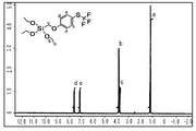
- FIG. 1 shows the NMR spectrum of Compound 1.
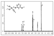
- FIG. 2 shows the NMR spectrum of Compound 2.
- FIG. 3 shows the NMR spectrum of Compound 3.
- FIG. 4 shows the NMR spectrum of Compound 4.
- FIG. 5 shows the NMR spectrum of Compound 5.
- FIG. 6 shows the NMR spectrum of Compound 6.
- FIG. 7 shows the NMR spectrum of Comparative Compound 1.
- the present invention includes a hydrolyzable silane, a hydrolyzate thereof, or a hydrolyzate condensate thereof as a silane, the hydrolyzable silane comprising a hydrolyzable silane represented by the formula (1), and silicon in the entire silane.
- R 1 represents an organic group represented by the formula (2) and is bonded to a silicon atom by a Si—C bond.
- R 2 represents an organic group having an alkyl group, an aryl group, a halogenated alkyl group, a halogenated aryl group, an alkoxyaryl group, an alkenyl group, an epoxy group, an acryloyl group, a methacryloyl group, a mercapto group, an amino group, or a cyano group.
- R 3 represents an alkoxy group, an acyloxy group, or a halogen group.
- a represents an integer of 1
- b represents an integer of 0 to 2
- a + b represents an integer of 1 to 3.
- X and Y each represent an oxygen atom or a sulfur atom.
- X and Y are not the same atom at the same time. That is, the present invention shows a case where X is an oxygen atom and Y is a sulfur atom, or a case where X is a sulfur atom and Y is an oxygen atom.
- a sulfide bond can be formed by using a sulfur atom.
- An ether bond can be formed by using an oxygen atom.
- R 6 represents an optionally substituted alkyl group having 1 to 10 carbon atoms
- R 4 represents an optionally substituted alkylene group having 1 to 10 carbon atoms
- R 5 represents an optionally substituted alkyl group.
- n represents an integer of 0 to 4.
- the portion of R 4 is bonded to the Si atom.
- the silane represented by the formula (1) in all the silanes is 50 mol% or less, or 5 to 50 mol%, 7 to 50 mol%, 7 to 40 mol%, 7 to 35 mol%, or 7 to 30 mol. Mol%, or 7 to 20 mol%, or 10 to 50 mol%, or 10 to 45 mol%, or 10 to 40 mol%, or 10 to 35 mol%, or 10 to 30 mol%, or 7 to 20 mol% % Can be used.
- the resist underlayer film forming composition of the present invention is a hydrolyzable silane represented by the formula (1), or a hydrolyzable silane represented by the formula (1) and other hydrolyzable silanes (for example, represented by the formula (3)). Hydrolyzable silane), its hydrolyzate, or its hydrolysis condensate, and a solvent. As optional components, acid, water, alcohol, curing catalyst, acid generator, other organic polymer, light-absorbing compound, surfactant and the like can be included.
- the solid content in the resist underlayer film forming composition of the present invention is, for example, 0.1 to 50% by mass, or 0.1 to 30% by mass, and 0.1 to 25% by mass.
- the solid content is obtained by removing the solvent component from all the components of the resist underlayer film forming composition.
- the ratio of the hydrolyzable silane, its hydrolyzate, and its hydrolysis condensate in the solid content is 20% by mass or more, for example, 50 to 100% by mass, 60 to 99% by mass, 70 to 99% by mass. It is.
- the alkyl group may be a linear or branched alkyl group having 1 to 10 carbon atoms, such as a methyl group, an ethyl group, an n-propyl group, an i-propyl group, an n-butyl group, an i- Butyl, s-butyl, t-butyl, n-pentyl, 1-methyl-n-butyl, 2-methyl-n-butyl, 3-methyl-n-butyl, 1,1-dimethyl -N-propyl group, 1,2-dimethyl-n-propyl group, 2,2-dimethyl-n-propyl group, 1-ethyl-n-propyl group, n-hexyl, 1-methyl-n-pentyl group, 2-methyl-n-pentyl group, 3-methyl-n-pentyl group, 4-methyl-n-pentyl group, 1,1-dimethyl-n-butyl group, 1,2-dimethyl-n
- a cyclic alkyl group can also be used.
- a cyclic alkyl group having 1 to 10 carbon atoms includes a cyclopropyl group, a cyclobutyl group, a 1-methyl-cyclopropyl group, a 2-methyl-cyclopropyl group, a cyclopentyl group, 1-methyl-cyclobutyl group, 2-methyl-cyclobutyl group, 3-methyl-cyclobutyl group, 1,2-dimethyl-cyclopropyl group, 2,3-dimethyl-cyclopropyl group, 1-ethyl-cyclopropyl group, 2 -Ethyl-cyclopropyl group, cyclohexyl group, 1-methyl-cyclopentyl group, 2-methyl-cyclopentyl group, 3-methyl-cyclopentyl group, 1-ethyl-cyclobutyl group, 2-ethyl-cyclobutyl group, 3-ethyl-cyclobutyl Group, 1,2-di
- alkylene group examples include an alkylene group derived from the alkyl group.
- a methyl group includes a methylene group
- an ethyl group includes an ethylene group
- a propyl group includes a propylene group.
- alkenyl group examples include alkenyl groups having 2 to 10 carbon atoms, including ethenyl group, 1-propenyl group, 2-propenyl group, 1-methyl-1-ethenyl group, 1-butenyl group, 2-butenyl group, 3-butenyl group, 2-methyl-1-propenyl group, 2-methyl-2-propenyl group, 1-ethylethenyl group, 1-methyl-1-propenyl group, 1-methyl-2-propenyl group, 1-pentenyl group 2-pentenyl group, 3-pentenyl group, 4-pentenyl group, 1-n-propylethenyl group, 1-methyl-1-butenyl group, 1-methyl-2-butenyl group, 1-methyl-3-butenyl group Group, 2-ethyl-2-propenyl group, 2-methyl-1-butenyl group, 2-methyl-2-butenyl group, 2-methyl-3-butenyl group, 3-methyl-1-butenyl group, 3- Tyl-2-
- aryl group examples include aryl groups having 6 to 20 carbon atoms, such as a phenyl group, o-methylphenyl group, m-methylphenyl group, p-methylphenyl group, o-chlorophenyl group, m-chlorophenyl.
- organic group having an epoxy group examples include glycidoxymethyl, glycidoxyethyl, glycidoxypropyl, glycidoxybutyl, and epoxycyclohexyl.
- Examples of the organic group having an acryloyl group include acryloylmethyl, acryloylethyl, acryloylpropyl, and the like.
- Examples of the organic group having a methacryloyl group include methacryloylmethyl, methacryloylethyl, methacryloylpropyl, and the like.
- Examples of the organic group having a mercapto group include ethyl mercapto, butyl mercapto, hexyl mercapto, and octyl mercapto.
- Examples of the organic group having an amino group include aminomethyl, aminoethyl, aminopropyl, and the like.
- Examples of the organic group having a cyano group include cyanoethyl and cyanopropyl.
- alkoxy group examples include alkoxy groups having a linear, branched, or cyclic alkyl portion having 1 to 20 carbon atoms, such as a methoxy group, an ethoxy group, an n-propoxy group, an i-propoxy group, and an n-butoxy group.
- acyloxy group examples include acyloxy groups having 2 to 20 carbon atoms, such as methylcarbonyloxy group, ethylcarbonyloxy group, n-propylcarbonyloxy group, i-propylcarbonyloxy group, n-butylcarbonyloxy group.
- halogen group examples include fluorine, chlorine, bromine and iodine. These examples also apply to the halogen group portion of the halogenated alkyl group and the halogenated aryl group.
- hydrolyzable silane represented by the formula (1) are as follows.
- the hydrolyzable silane is a combination of a hydrolyzable silane represented by the formula (1) and another hydrolyzable silane, and the other hydrolyzable silanes are represented by the following formulas (3) and (4).
- R 7 has an alkyl group, an aryl group, a halogenated alkyl group, a halogenated aryl group, an alkoxyaryl group, an alkenyl group, or an epoxy group, an acryloyl group, a methacryloyl group, a mercapto group, or a cyano group.
- R 8 represents an alkoxy group, an acyloxy group, or a halogen group
- c represents an integer of 0 to 3.
- R 9 represents an alkyl group and is bonded to a silicon atom by a Si—C bond
- R 10 represents an alkoxy group, an acyloxy group, or a halogen group
- Y R represents an alkylene group.
- d represents an integer of 0 or 1
- e represents an integer of 0 or 1.
- the organic group having a cyano group, an alkoxy group, an acyloxy group, a halogen group, an alkylene group, and an arylene group the above-described examples can be used.
- Examples of the silicon-containing compound represented by the formula (3) include tetramethoxysilane, tetrachlorosilane, tetraacetoxysilane, tetraethoxysilane, tetra n-propoxysilane, tetraisopropoxysilane, tetra n-butoxysilane, and methyltrimethoxysilane.
- Methyltrichlorosilane methyltriacetoxysilane, methyltripropoxysilane, methyltributoxysilane, methyltriamyloxysilane, methyltriphenoxysilane, methyltribenzyloxysilane, methyltriphenethyloxysilane, glycidoxymethyltrimethoxysilane , Glycidoxymethyltriethoxysilane, ⁇ -glycidoxyethyltrimethoxysilane, ⁇ -glycidoxyethyltriethoxysilane, ⁇ -glycidoxyethyltrimethoxysilane ⁇ -glycidoxyethyltriethoxysilane, ⁇ -glycidoxypropyltrimethoxysilane, ⁇ -glycidoxypropyltriethoxysilane, ⁇ -glycidoxypropyltrimethoxysilane, ⁇ -glycidoxypropyltriethoxy
- hydrolyzable silanes can also be used.
- Examples of the silicon-containing compound represented by the formula (4) include methylene bistrimethoxysilane, methylene bistrichlorosilane, methylene bistriacetoxysilane, ethylene bistriethoxysilane, ethylene bistrichlorosilane, ethylene bistriacetoxysilane, propylene bistriethoxysilane, and butylene bistrimethoxysilane.
- a silane having a sulfone group or a silane having a sulfonamide group can be used as the hydrolyzable silane, and examples thereof include the following.
- hydrolysis condensate polysiloxane
- the hydrolyzable condensate (polyorganosiloxane) of the hydrolyzable silane can obtain a condensate having a weight average molecular weight of 1,000 to 1,000,000, or 1,000 to 100,000. These molecular weights are molecular weights obtained in terms of polystyrene by GPC analysis.
- GPC measurement conditions are, for example, GPC apparatus (trade name HLC-8220 GPC, manufactured by Tosoh Corporation), GPC column (trade names Shodex KF803L, KF802, KF801, Showa Denko), column temperature is 40 ° C., and eluent (elution solvent) Is tetrahydrofuran, the flow rate (flow rate) is 1.0 ml / min, and the standard sample is polystyrene (manufactured by Showa Denko KK).
- hydrolysis of the alkoxysilyl group, acyloxysilyl group, or halogenated silyl group 0.5 to 100 mol, preferably 1 to 10 mol of water is used per mol of the hydrolyzable group. Further, 0.001 to 10 mol, preferably 0.001 to 1 mol of hydrolysis catalyst can be used per mol of the hydrolyzable group.
- the reaction temperature during the hydrolysis and condensation is usually 20 to 80 ° C.
- Hydrolysis may be performed completely or partially. That is, a hydrolyzate or a monomer may remain in the hydrolysis condensate.
- a catalyst can be used in the hydrolysis and condensation. Examples of the hydrolysis catalyst include metal chelate compounds, organic acids, inorganic acids, organic bases, and inorganic bases.
- Examples of the metal chelate compound as the hydrolysis catalyst include triethoxy mono (acetylacetonato) titanium, tri-n-propoxy mono (acetylacetonato) titanium, tri-i-propoxy mono (acetylacetonato) titanium, tri -N-Butoxy mono (acetylacetonato) titanium, tri-sec-butoxy mono (acetylacetonato) titanium, tri-t-butoxy mono (acetylacetonato) titanium, diethoxy bis (acetylacetonato) titanium , Di-n-propoxy bis (acetylacetonato) titanium, di-i-propoxy bis (acetylacetonato) titanium, di-n-butoxy bis (acetylacetonato) titanium, di-sec-butoxy bis (Acetylacetonate) Titanium, Di-t- Toxi-bis (acetylacetonato) titanium, monoethoxy-tris (acetylaceton
- Organic acids as hydrolysis catalysts are, for example, acetic acid, propionic acid, butanoic acid, pentanoic acid, hexanoic acid, heptanoic acid, octanoic acid, nonanoic acid, decanoic acid, oxalic acid, maleic acid, methylmalonic acid, adipic acid, sebacin Acid, gallic acid, butyric acid, merit acid, arachidonic acid, 2-ethylhexanoic acid, oleic acid, stearic acid, linoleic acid, linolenic acid, salicylic acid, benzoic acid, p-aminobenzoic acid, p-toluenesulfonic acid, benzenesulfone Examples include acid, monochloroacetic acid, dichloroacetic acid, trichloroacetic acid, trifluoroacetic acid, formic acid, malonic acid, sulfonic acid, phthal
- Organic bases as hydrolysis catalysts include, for example, pyridine, pyrrole, piperazine, pyrrolidine, piperidine, picoline, trimethylamine, triethylamine, monoethanolamine, diethanolamine, dimethylmonoethanolamine, monomethyldiethanolamine, triethanolamine, diazabicyclooctane, diazine.
- Examples include zabicyclononane, diazabicycloundecene, and tetramethylammonium hydroxide.
- the inorganic base include ammonia, sodium hydroxide, potassium hydroxide, barium hydroxide, calcium hydroxide and the like. Of these catalysts, metal chelate compounds, organic acids, and inorganic acids are preferred, and these may be used alone or in combination of two or more.
- organic solvent used in the hydrolysis examples include n-pentane, i-pentane, n-hexane, i-hexane, n-heptane, i-heptane, 2,2,4-trimethylpentane, n-octane, i- Aliphatic hydrocarbon solvents such as octane, cyclohexane and methylcyclohexane; benzene, toluene, xylene, ethylbenzene, trimethylbenzene, methylethylbenzene, n-propyl benzene, i-propyl benzene, diethylbenzene, i-butylbenzene, triethylbenzene, di -Aromatic hydrocarbon solvents such as i-propyl benzene, n-amyl naphthalene, trimethylbenzene; methanol, ethanol, ethanol
- acetone methyl ethyl ketone, methyl-n-propyl ketone, methyl-n-butyl ketone, diethyl ketone, methyl-i-butyl ketone, methyl-n-pentyl ketone, ethyl-n-butyl ketone, methyl-n-hexyl ketone, di- Ketone solvents such as i-butyl ketone, trimethylnonanone, cyclohexanone, methylcyclohexanone, 2,4-pentanedione, acetonylacetone, diacetone alcohol, acetophenone, and fenchon are preferred from the viewpoint of storage stability of the solution.
- bisphenol S or a bisphenol S derivative can be added as an additive.
- Bisphenol S or a bisphenol S derivative is 0.01 to 20 parts by mass, 0.01 to 10 parts by mass, or 0.01 to 5 parts by mass with respect to 100 parts by mass of the polyorganosiloxane.
- Preferred bisphenol S or bisphenol S derivatives are exemplified below.
- the resist underlayer film forming composition of the present invention can contain a curing catalyst.
- the curing catalyst functions as a curing catalyst when a coating film containing polyorganosiloxane composed of a hydrolysis condensate is heated and cured.
- As the curing catalyst ammonium salts, phosphines, phosphonium salts, and sulfonium salts can be used.
- the formula (D-1) Wherein m is an integer of 2 to 11, n 1 is an integer of 2 to 3, R 21 is an alkyl group or an aryl group, and Y A - is an anion.
- the formula (D-7) (However, R 31 , R 32 , R 33 , and R 34 represent an alkyl group or an aryl group, P represents a phosphorus atom, Y A ⁇ represents an anion, and R 31 , R 32 , R 33 , and R 34 are each linked to a phosphorus atom by a CP bond).
- the formula (D-8) (However, R 35 , R 36 and R 37 represent an alkyl group or an aryl group, S represents a sulfur atom, Y A ⁇ represents an anion, and R 35 , R 36 and R 37 represent C—S, respectively. And a tertiary sulfonium salt which is bonded to a sulfur atom by a bond).
- the compound represented by the above formula (D-1) is a quaternary ammonium salt derived from an amine, m represents an integer of 2 to 11, and n 1 represents an integer of 2 to 3.
- R 21 of this quaternary ammonium salt represents an alkyl group having 1 to 18 carbon atoms, preferably 2 to 10 carbon atoms, or an aryl group.
- a linear alkyl group such as an ethyl group, a propyl group, or a butyl group
- Examples include a benzyl group, a cyclohexyl group, a cyclohexylmethyl group, and a dicyclopentadienyl group.
- Anions (Y A ⁇ ) include halogen ions such as chlorine ions (Cl ⁇ ), bromine ions (Br ⁇ ), iodine ions (I ⁇ ), carboxylates (—COO ⁇ ), sulfonates (—SO 3 — ). And acid groups such as alcoholate (—O ⁇ ).
- R 22 R 23 R 24 R 25 N + Y A - is a quaternary ammonium salt represented by.
- R 22 , R 23 , R 24 and R 25 are an alkyl group or aryl group having 1 to 18 carbon atoms, or a silane compound bonded to a silicon atom by a Si—C bond.
- the anion (Y A ⁇ ) is a halogen ion such as chlorine ion (Cl ⁇ ), bromine ion (Br ⁇ ), iodine ion (I ⁇ ), carboxylate (—COO ⁇ ), sulfonate (—SO 3 ⁇ ).
- This quaternary ammonium salt can be obtained commercially, for example, tetramethylammonium acetate, tetrabutylammonium acetate, triethylbenzylammonium chloride, triethylbenzylammonium bromide, trioctylmethylammonium chloride, tributylbenzyl chloride. Examples include ammonium and trimethylbenzylammonium chloride.
- the compound represented by the above formula (D-3) is a quaternary ammonium salt derived from 1-substituted imidazole, and R 26 and R 27 are each an alkyl group having 1 to 18 carbon atoms or an aryl group. It is preferable that the total number of carbon atoms of R 26 and R 27 is 7 or more.
- R 26 can be exemplified by methyl group, ethyl group, propyl group, phenyl group and benzyl group
- R 27 can be exemplified by benzyl group, octyl group and octadecyl group.
- the anion (Y A ⁇ ) is a halogen ion such as chlorine ion (Cl ⁇ ), bromine ion (Br ⁇ ), iodine ion (I ⁇ ), carboxylate (—COO ⁇ ), sulfonate (—SO 3 ⁇ ). And acid groups such as alcoholate (—O ⁇ ).
- This compound can be obtained as a commercial product. For example, imidazole compounds such as 1-methylimidazole and 1-benzylimidazole are reacted with alkyl halides and aryl halides such as benzyl bromide and methyl bromide. Can be manufactured.
- the compound represented by the above formula (D-4) is a quaternary ammonium salt derived from pyridine, and R 28 is an alkyl group having 1 to 18 carbon atoms, preferably 4 to 18 carbon atoms, or Examples of the aryl group include a butyl group, an octyl group, a benzyl group, and a lauryl group.
- the anion (Y A ⁇ ) is a halogen ion such as chlorine ion (Cl ⁇ ), bromine ion (Br ⁇ ), iodine ion (I ⁇ ), carboxylate (—COO ⁇ ), sulfonate (—SO 3 ⁇ ).
- this compound can be obtained as a commercial product, it is produced, for example, by reacting pyridine with an alkyl halide such as lauryl chloride, benzyl chloride, benzyl bromide, methyl bromide, octyl bromide, or an aryl halide. I can do it. Examples of this compound include N-laurylpyridinium chloride and N-benzylpyridinium bromide.
- the compound represented by the above formula (D-5) is a quaternary ammonium salt derived from a substituted pyridine represented by picoline or the like, and R 29 has 1 to 18 carbon atoms, preferably 4 to 18 carbon atoms.
- R 29 has 1 to 18 carbon atoms, preferably 4 to 18 carbon atoms.
- the alkyl group or aryl group include a methyl group, an octyl group, a lauryl group, and a benzyl group.
- R 30 is an alkyl group having 1 to 18 carbon atoms or an aryl group. For example, in the case of quaternary ammonium derived from picoline, R 30 is a methyl group.
- the anion (Y A ⁇ ) is a halogen ion such as chlorine ion (Cl ⁇ ), bromine ion (Br ⁇ ), iodine ion (I ⁇ ), carboxylate (—COO ⁇ ), sulfonate (—SO 3 ⁇ ). And acid groups such as alcoholate (—O ⁇ ).
- This compound can also be obtained as a commercial product. For example, a substituted pyridine such as picoline is reacted with an alkyl halide such as methyl bromide, octyl bromide, lauryl chloride, benzyl chloride or benzyl bromide, or an aryl halide. Can be manufactured. Examples of this compound include N-benzylpicolinium chloride, N-benzylpicolinium bromide, N-laurylpicolinium chloride and the like.
- the compound represented by the above formula (D-6) is a tertiary ammonium salt derived from an amine, m represents an integer of 2 to 11, and n 1 represents an integer of 2 to 3.
- Anions (Y A ⁇ ) include halogen ions such as chlorine ions (Cl ⁇ ), bromine ions (Br ⁇ ), iodine ions (I ⁇ ), carboxylates (—COO ⁇ ), sulfonates (—SO 3 — ). And acid groups such as alcoholate (—O ⁇ ). It can be produced by reacting an amine with a weak acid such as carboxylic acid or phenol. Examples of the carboxylic acid include formic acid and acetic acid.
- the anion (Y A ⁇ ) When formic acid is used, the anion (Y A ⁇ ) is (HCOO ⁇ ), and when acetic acid is used, the anion (Y A ⁇ ) is (CH 3 COO ⁇ ). When phenol is used, the anion (Y A ⁇ ) is (C 6 H 5 O ⁇ ).
- the compound represented by the above formula (D-7) is a quaternary phosphonium salt having a structure of R 31 R 32 R 33 R 34 P + Y A — .
- R 31 , R 32 , R 33 , and R 34 are an alkyl group having 1 to 18 carbon atoms, an aryl group, or a silane compound bonded to a silicon atom by a Si—C bond, and preferably R 31 or three among the four substituents of R 34 is a phenyl group or substituted phenyl group, for example, can be exemplified a phenyl group or a tolyl group, also remaining one of 1 to 18 carbon atoms A silane compound bonded to a silicon atom through an alkyl group, an aryl group, or a Si—C bond.
- Anions (Y A ⁇ ) include halogen ions such as chlorine ions (Cl ⁇ ), bromine ions (Br ⁇ ), iodine ions (I ⁇ ), carboxylates (—COO ⁇ ), sulfonates (—SO 3 — ). And acid groups such as alcoholate (—O ⁇ ).
- This compound can be obtained as a commercial product, for example, a halogenated tetraalkylphosphonium such as tetra-n-butylphosphonium halide, tetra-n-propylphosphonium halide, or a trialkylbenzyl halide such as triethylbenzylphosphonium halide.
- Triphenylmonoalkylphosphonium halides such as phosphonium, triphenylmethylphosphonium halide, triphenylethylphosphonium halide, triphenylbenzylphosphonium halide, tetraphenylphosphonium halide, tritolylmonoarylphosphonium halide, or tritolyl monohalogenate Examples thereof include alkylphosphonium (the halogen atom is a chlorine atom or a bromine atom).
- halogens such as triphenylmonoalkylphosphonium halides such as triphenylmethylphosphonium halide, triphenylethylphosphonium halide, triphenylmonoarylphosphonium halides such as triphenylbenzylphosphonium halide, and halogens such as tritolylmonophenylphosphonium halide.
- Preferred is a tolylyl monoarylphosphonium halide, or a tolyl monoalkylphosphonium halide such as a tolyl monomethylphosphonium halide (the halogen atom is a chlorine atom or a bromine atom).
- the phosphines include methylphosphine, ethylphosphine, propylphosphine, isopropylphosphine, isobutylphosphine, phenylphosphine and other first phosphine, dimethylphosphine, diethylphosphine, diisopropylphosphine, diisoamylphosphine, diphenylphosphine and other second phosphine.
- tertiary phosphines such as trimethylphosphine, triethylphosphine, triphenylphosphine, methyldiphenylphosphine, and dimethylphenylphosphine.
- R 35 R 36 R 37 S + Y A - is a tertiary sulfonium salt having a structure.
- R 35 , R 36 , and R 37 are an alkyl group having 1 to 18 carbon atoms, an aryl group, or a silane compound that is bonded to a silicon atom by a Si—C bond, and preferably R 35 to R 37.
- substituents are phenyl groups or substituted phenyl groups, for example, a phenyl group or a tolyl group, and the other one is an alkyl group having 1 to 18 carbon atoms, Or it is an aryl group.
- Anions (Y A ⁇ ) include halogen ions such as chlorine ions (Cl ⁇ ), bromine ions (Br ⁇ ), iodine ions (I ⁇ ), carboxylates (—COO ⁇ ), sulfonates (—SO 3 — ). ), Alcoholate (—O ⁇ ), maleate anion, nitrate anion and the like. This compound is available as a commercial product.
- halogenated tetraalkylsulfonium such as tri-n-butylsulfonium halide and tri-n-propylsulfonium halide
- trialkylbenzyl halide such as diethylbenzylsulfonium halide.
- a nitrogen-containing silane compound can be added as a curing catalyst.
- the nitrogen-containing silane compound include imidazole ring-containing silane compounds such as N- (3-triethoxysilylpropyl) -4,5-dihydroimidazole.
- the curing catalyst is 0.01 to 10 parts by mass, 0.01 to 5 parts by mass, or 0.01 to 3 parts by mass with respect to 100 parts by mass of the polyorganosiloxane.
- Hydrolyzable silane is hydrolyzed using a catalyst in a solvent to condense, and the resulting hydrolyzed condensate (polymer) simultaneously removes by-product alcohol, used hydrolysis catalyst, and water by distillation under reduced pressure. be able to.
- the acid and base catalyst used for hydrolysis can be removed by neutralization or ion exchange.
- an organic acid, water, alcohol, or a combination thereof can be added to the resist underlayer film forming composition containing the hydrolysis condensate for stabilization. .
- organic acid examples include oxalic acid, malonic acid, methylmalonic acid, succinic acid, maleic acid, malic acid, tartaric acid, phthalic acid, citric acid, glutaric acid, citric acid, lactic acid, and salicylic acid. Of these, oxalic acid and maleic acid are preferred.
- the organic acid to be added is 0.1 to 5.0 parts by mass with respect to 100 parts by mass of the condensate (polyorganosiloxane).
- pure water, ultrapure water, ion exchange water, etc. can be used for the water to add, and the addition amount can be 1-20 mass parts with respect to 100 mass parts of resist underlayer film forming compositions.
- alcohol to add what is easy to be scattered by the heating after application
- coating is preferable, for example, methanol, ethanol, propanol, isopropanol, a butanol etc. are mentioned.
- the added alcohol can be 1 to 20 parts by mass with respect to 100 parts by mass of the resist underlayer film forming composition.
- the underlayer film forming composition for lithography of the present invention can contain an organic polymer compound, a photoacid generator, a surfactant, and the like as necessary in addition to the above components.
- the dry etching rate (thickness reduction per unit time), attenuation coefficient, refractive index, etc. of the resist underlayer film formed from the underlayer film forming composition for lithography of the present invention are adjusted. can do.
- organic polymer compound there is no restriction
- Polycondensation polymers and addition polymerization polymers can be used.
- Addition polymerization polymers and condensation polymerization polymers such as polyester, polystyrene, polyimide, acrylic polymer, methacrylic polymer, polyvinyl ether, phenol novolak, naphthol novolak, polyether, polyamide, and polycarbonate can be used.
- organic polymer having an aromatic ring structure such as a benzene ring, a naphthalene ring, an anthracene ring, a triazine ring, a quinoline ring, and a quinoxaline ring that functions as a light absorption site is preferably used.
- organic polymer compounds include addition polymerizable monomers such as benzyl acrylate, benzyl methacrylate, phenyl acrylate, naphthyl acrylate, anthryl methacrylate, anthryl methyl methacrylate, styrene, hydroxystyrene, benzyl vinyl ether, and N-phenylmaleimide.
- addition-polymerized polymers containing as a structural unit, and polycondensation polymers such as phenol novolac and naphthol novolak.
- the polymer compound When an addition polymerization polymer is used as the organic polymer compound, the polymer compound may be a homopolymer or a copolymer.
- An addition polymerizable monomer is used for the production of the addition polymerization polymer.
- examples of such addition polymerizable monomers include acrylic acid, methacrylic acid, acrylic ester compounds, methacrylic ester compounds, acrylamide compounds, methacrylamide compounds, vinyl compounds, styrene compounds, maleimide compounds, maleic anhydride, acrylonitrile and the like. It is done.
- acrylic ester compounds include methyl acrylate, ethyl acrylate, normal hexyl acrylate, isopropyl acrylate, cyclohexyl acrylate, benzyl acrylate, phenyl acrylate, anthryl methyl acrylate, 2-hydroxyethyl acrylate, 3-chloro-2-hydroxypropyl acrylate, 2-hydroxypropyl acrylate, 2,2,2-trifluoroethyl acrylate, 2,2,2-trichloroethyl acrylate, 2-bromoethyl acrylate, 4-hydroxybutyl acrylate, 2-methoxyethyl acrylate, tetrahydrofurfuryl acrylate, 2-Methyl-2-adamantyl acrylate, 5-acryloyloxy-6-hydroxynorbornene-2-carboxy Examples include ric-6-lactone, 3-acryloxypropyltriethoxysilane, and glycidyl acrylate
- Methacrylic acid ester compounds include methyl methacrylate, ethyl methacrylate, normal hexyl methacrylate, isopropyl methacrylate, cyclohexyl methacrylate, benzyl methacrylate, phenyl methacrylate, anthryl methyl methacrylate, 2-hydroxyethyl methacrylate, 2-hydroxypropyl methacrylate, 2,2, 2-trifluoroethyl methacrylate, 2,2,2-trichloroethyl methacrylate, 2-bromoethyl methacrylate, 4-hydroxybutyl methacrylate, 2-methoxyethyl methacrylate, tetrahydrofurfuryl methacrylate, 2-methyl-2-adamantyl methacrylate, 5 -Methacryloyloxy-6-hydroxynorbornene-2-carboxylic Examples include -6-lactone, 3-methacryloxypropyltriethoxysilane,
- Examples of acrylamide compounds include acrylamide, N-methyl acrylamide, N-ethyl acrylamide, N-benzyl acrylamide, N-phenyl acrylamide, N, N-dimethyl acrylamide and N-anthryl acrylamide.
- Examples of methacrylamide compounds include methacrylamide, N-methyl methacrylamide, N-ethyl methacrylamide, N-benzyl methacrylamide, N-phenyl methacrylamide, N, N-dimethyl methacrylamide and N-anthryl acrylamide.
- vinyl compounds include vinyl alcohol, 2-hydroxyethyl vinyl ether, methyl vinyl ether, ethyl vinyl ether, benzyl vinyl ether, vinyl acetic acid, vinyl trimethoxysilane, 2-chloroethyl vinyl ether, 2-methoxyethyl vinyl ether, vinyl naphthalene, and vinyl anthracene. Can be mentioned.
- styrene compound examples include styrene, hydroxystyrene, chlorostyrene, bromostyrene, methoxystyrene, cyanostyrene, and acetylstyrene.
- maleimide compounds include maleimide, N-methylmaleimide, N-phenylmaleimide, N-cyclohexylmaleimide, N-benzylmaleimide and N-hydroxyethylmaleimide.
- examples of such a polymer include a polycondensation polymer of a glycol compound and a dicarboxylic acid compound.
- examples of the glycol compound include diethylene glycol, hexamethylene glycol, butylene glycol and the like.
- examples of the dicarboxylic acid compound include succinic acid, adipic acid, terephthalic acid, maleic anhydride and the like.
- examples thereof include polyesters such as polypyromellitimide, poly (p-phenylene terephthalamide), polybutylene terephthalate, polyethylene terephthalate, polyamide, and polyimide.
- the organic polymer compound contains a hydroxyl group
- this hydroxyl group can form a crosslinking reaction with the polyorganosiloxane.
- a polymer compound having a weight average molecular weight of, for example, 1,000 to 1,000,000, 3,000 to 300,000, 5,000 to 200,000, or 10,000 to 100,000 can be used. Only one organic polymer compound can be used, or two or more organic polymer compounds can be used in combination.
- the proportion thereof is 1 to 200 parts by mass, 5 to 100 parts by mass, or 10 to 50 parts by mass, or 20 with respect to 100 parts by mass of the condensate (polyorganosiloxane). Thru
- the resist underlayer film forming composition of the present invention may contain an acid generator.
- the acid generator include a thermal acid generator and a photoacid generator.
- the photoacid generator generates an acid upon exposure of the resist. Therefore, the acidity of the lower layer film can be adjusted. This is a method for matching the acidity of the lower layer film with the acidity of the upper layer resist. Further, the pattern shape of the resist formed in the upper layer can be adjusted by adjusting the acidity of the lower layer film.
- Examples of the photoacid generator contained in the resist underlayer film forming composition of the present invention include onium salt compounds, sulfonimide compounds, and disulfonyldiazomethane compounds.
- onium salt compounds include diphenyliodonium hexafluorophosphate, diphenyliodonium trifluoromethanesulfonate, diphenyliodonium nonafluoronormalbutanesulfonate, diphenyliodonium perfluoronormaloctanesulfonate, diphenyliodoniumcamphorsulfonate, bis (4-tert-butylphenyl) iodoniumcamphor.
- Iodonium salt compounds such as sulfonate and bis (4-tert-butylphenyl) iodonium trifluoromethanesulfonate, and triphenylsulfonium hexafluoroantimonate, triphenylsulfonium nonafluoronormal butanesulfonate, triphenylsulfonium camphorsulfonate, and triphenyls Sulfonium salt compounds such as phosphonium trifluoromethanesulfonate, and the like.
- sulfonimide compounds include N- (trifluoromethanesulfonyloxy) succinimide, N- (nonafluoronormalbutanesulfonyloxy) succinimide, N- (camphorsulfonyloxy) succinimide and N- (trifluoromethanesulfonyloxy) naphthalimide. Can be mentioned.
- disulfonyldiazomethane compound examples include bis (trifluoromethylsulfonyl) diazomethane, bis (cyclohexylsulfonyl) diazomethane, bis (phenylsulfonyl) diazomethane, bis (p-toluenesulfonyl) diazomethane, and bis (2,4-dimethylbenzenesulfonyl). And diazomethane, and methylsulfonyl-p-toluenesulfonyldiazomethane.
- a photo-acid generator can use only 1 type, or can be used in combination of 2 or more type.
- the proportion thereof is 0.01 to 5 parts by mass, 0.1 to 3 parts by mass, or 0.5 with respect to 100 parts by mass of the condensate (polyorganosiloxane). Thru
- the surfactant is effective in suppressing the occurrence of pinholes and installations when the resist underlayer film forming composition for lithography of the present invention is applied to a substrate.
- the surfactant contained in the resist underlayer film forming composition of the present invention include polyoxyethylene alkyl ethers such as polyoxyethylene lauryl ether, polyoxyethylene stearyl ether, polyoxyethylene cetyl ether, and polyoxyethylene oleyl ether.
- surfactants may be used alone or in combination of two or more.
- the ratio is 0.0001 to 5 parts by mass, or 0.001 to 1 part by mass, or 0.01 to 1 with respect to 100 parts by mass of the condensate (polyorganosiloxane). Part by mass.
- a rheology adjusting agent, an adhesion aid and the like can be added to the resist underlayer film forming composition of the present invention.
- the rheology modifier is effective for improving the fluidity of the underlayer film forming composition.
- the adhesion aid is effective for improving the adhesion between the semiconductor substrate or resist and the lower layer film.
- the solvent used in the resist underlayer film forming composition of the present invention can be used without particular limitation as long as it is a solvent that can dissolve the solid content.
- solvents include methyl cellosolve acetate, ethyl cellosolve acetate, propylene glycol, propylene glycol monomethyl ether, propylene glycol monoethyl ether, methyl isobutyl carbinol, propylene glycol monobutyl ether, propylene glycol monomethyl ether acetate, propylene glycol mono Ether ether acetate, propylene glycol monopropyl ether acetate, propylene glycol monobutyl ether acetate, toluene, xylene, methyl ethyl ketone, cyclopentanone, cyclohexanone, ethyl 2-hydroxypropionate, ethyl 2-hydroxy-2-methylpropionate, ethyl ethoxyacetate , Ethyl
- a resist underlayer film is formed on the substrate by a coating method, or a resist underlayer film is formed thereon by an organic underlayer film on the substrate, A resist film (for example, a photoresist or an electron beam resist) is formed on the resist underlayer film. Then, a resist pattern is formed by exposure and development, and the resist underlayer film is dry-etched using the resist pattern to transfer the pattern, and the substrate is processed by the pattern, or the organic underlayer film is etched by pattern transfer. Then, the substrate is processed with the organic underlayer film.
- a resist film for example, a photoresist or an electron beam resist
- the resist film thickness tends to be thin in order to prevent pattern collapse.
- dry etching for transferring a pattern to a film existing in a lower layer by reducing the thickness of the resist, the pattern cannot be transferred unless the etching rate is higher than that of the upper layer.
- the resist underlayer film (containing an inorganic silicon compound) of the present invention is coated on the substrate with or without an organic underlayer film, and a resist film (organic resist) is formed thereon. Film).
- the organic component film and the inorganic component film differ greatly in the dry etching rate depending on the selection of the etching gas.
- the organic component film has an oxygen-based gas and the dry etching rate increases.
- the inorganic component film has a halogen-containing gas. This increases the dry etching rate.
- a resist pattern is formed, and the resist underlayer film of the present invention existing under the resist pattern is dry-etched with a halogen-containing gas to transfer the pattern to the resist underlayer film, and the pattern transferred to the resist underlayer film contains halogen.
- Substrate processing is performed using gas.
- the organic underlayer film under the layer is dry-etched with an oxygen-based gas to transfer the pattern to the organic underlayer film, and the pattern-transferred organic underlayer film is halogen-containing.
- Substrate processing is performed using gas.
- the resist underlayer film forming composition of the present invention is applied onto a coated substrate or the like by an appropriate application method such as a spinner or a coater, and then baked to form a resist underlayer film.
- the conditions for firing are appropriately selected from firing temperatures of 80 ° C. to 250 ° C. and firing times of 0.3 to 60 minutes.
- the firing temperature is 150 ° C. to 250 ° C.
- the firing time is 0.5 to 2 minutes.
- the thickness of the formed lower layer film is, for example, 10 to 1000 nm, 20 to 500 nm, 50 to 300 nm, or 100 to 200 nm.
- a photoresist layer is formed on the resist underlayer film. Formation of the photoresist layer can be performed by a well-known method, that is, by applying a photoresist composition solution onto the lower layer film and baking.
- the film thickness of the photoresist is, for example, 50 to 10,000 nm, 100 to 2000 nm, or 200 to 1000 nm.
- the resist underlayer film of the present invention can be formed thereon, and a photoresist can be further coated thereon.
- the substrate can be processed by selecting an appropriate etching gas.
- an appropriate etching gas For example, it is possible to process the resist underlayer film of the present invention using a fluorine-based gas that has a sufficiently high etching rate for photoresist as an etching gas, and a sufficiently high etching rate for the resist underlayer film of the present invention.
- the organic underlayer film can be processed using an oxygen-based gas as an etching gas, and the substrate can be processed using a fluorine-based gas that provides a sufficiently high etching rate for the organic underlayer film as an etching gas.
- the photoresist formed on the resist underlayer film of the present invention is not particularly limited as long as it is sensitive to light used for exposure. Either a negative photoresist or a positive photoresist can be used.
- a positive photoresist comprising a novolac resin and 1,2-naphthoquinonediazide sulfonic acid ester, a chemically amplified photoresist comprising a binder having a group that decomposes with an acid to increase the alkali dissolution rate and a photoacid generator, an acid
- a chemically amplified photoresist comprising a low-molecular compound that decomposes to increase the alkali dissolution rate of the photoresist, an alkali-soluble binder, and a photoacid generator, and a binder having a group that decomposes with an acid to increase the alkali dissolution rate
- a chemically amplified photoresist composed of a low molecular weight compound that de
- Examples include trade name APEX-E manufactured by Shipley, trade name PAR710 manufactured by Sumitomo Chemical Co., Ltd., and trade name SEPR430 manufactured by Shin-Etsu Chemical Co., Ltd. Also, for example, Proc. SPIE, Vol. 3999, 330-334 (2000), Proc. SPIE, Vol. 3999, 357-364 (2000), Proc. SPIE, Vol. 3999, 365-374 (2000), and fluorine-containing polymer-based photoresists.
- a KrF excimer laser (wavelength 248 nm), an ArF excimer laser (wavelength 193 nm), an F2 excimer laser (wavelength 157 nm), or the like can be used.
- post-exposure bake can be performed as necessary.
- the post-exposure heating is performed under conditions appropriately selected from a heating temperature of 70 ° C. to 150 ° C. and a heating time of 0.3 to 10 minutes.
- a resist for electron beam lithography or a resist for EUV lithography can be used instead of a photoresist as a resist.
- the electron beam resist either a negative type or a positive type can be used.
- Chemically amplified resist comprising a binder having a group that decomposes with an acid generator and an acid to change the alkali dissolution rate, a low molecular weight compound that decomposes with an alkali-soluble binder, an acid generator and an acid to change the alkali dissolution rate of the resist
- a chemically amplified resist comprising: a binder having a group that decomposes with an acid generator and an acid to change the alkali dissolution rate; and a chemically amplified resist comprising a low-molecular compound that decomposes with an acid to change the alkali dissolution rate of the resist,
- non-chemically amplified resists composed of a binder having a group that changes the alkali dissolution rate by being
- developer for example, an alkali developer
- Developers include aqueous solutions of alkali metal hydroxides such as potassium hydroxide and sodium hydroxide, aqueous solutions of quaternary ammonium hydroxides such as tetramethylammonium hydroxide, tetraethylammonium hydroxide and choline, ethanolamine, propylamine, An alkaline aqueous solution such as an aqueous amine solution such as ethylenediamine can be mentioned as an example. Further, a surfactant or the like can be added to these developers.
- the development conditions are appropriately selected from a temperature of 5 to 50 ° C. and a time of 10 to 600 seconds.
- an organic solvent can be used as a developer. After the exposure, development is performed with a developer (solvent). As a result, for example, when a positive photoresist is used, the unexposed portion of the photoresist is removed, and a photoresist pattern is formed.
- Developers include, for example, methyl acetate, butyl acetate, ethyl acetate, isopropyl acetate, amyl acetate, isoamyl acetate, ethyl methoxyacetate, ethyl ethoxy acetate, propylene glycol monomethyl ether acetate, ethylene glycol monoethyl ether acetate, ethylene glycol monopropyl Ether acetate, ethylene glycol monobutyl ether acetate, ethylene glycol monophenyl ether acetate, diethylene glycol monomethyl ether acetate, diethylene glycol monopropyl ether acetate, diethylene glycol monoethyl ether acetate, diethylene glycol monophenyl ether acetate, diethylene glycol monobutyl ether acetate, 2-methoxybutyl Cetate, 3-methoxybutyl acetate, 4-methoxybutyl acetate, 3-methyl-3-me
- the resist underlayer film (intermediate layer) of the present invention is removed using the photoresist (upper layer) pattern thus formed as a protective film, and then the patterned photoresist and the resist underlayer film of the present invention are removed.
- the organic underlayer film (lower layer) is removed using the film made of (intermediate layer) as a protective film.
- the semiconductor substrate is processed using the patterned resist underlayer film (intermediate layer) and organic underlayer film (lower layer) of the present invention as a protective film.
- the resist underlayer film (intermediate layer) of the present invention in a portion where the photoresist has been removed is removed by dry etching to expose the semiconductor substrate.
- dry etching of the resist underlayer film of the present invention tetrafluoromethane (CF 4 ), perfluorocyclobutane (C 4 F 8 ), perfluoropropane (C 3 F 8 ), trifluoromethane, carbon monoxide, argon, oxygen, Gases such as nitrogen, sulfur hexafluoride, difluoromethane, nitrogen trifluoride and chlorine trifluoride, chlorine, trichloroborane and dichloroborane can be used.
- a halogen-based gas for dry etching of the resist underlayer film.
- a photoresist made of an organic substance is basically difficult to remove.
- the resist underlayer film of the present invention containing a large amount of silicon atoms is quickly removed by the halogen-based gas. Therefore, it is possible to suppress a decrease in the thickness of the photoresist accompanying dry etching of the resist underlayer film. As a result, the photoresist can be used as a thin film.
- the dry etching of the resist underlayer film is preferably performed using a fluorine-based gas.
- fluorine-based gas examples include tetrafluoromethane (CF 4 ), perfluorocyclobutane (C 4 F 8 ), and perfluoropropane (C 3 F 8 ). , Trifluoromethane, and difluoromethane (CH 2 F 2 ).
- the organic underlayer film is removed using the patterned photoresist and the film made of the resist underlayer film of the present invention as a protective film.
- the organic underlayer film (underlayer) is preferably formed by dry etching with an oxygen-based gas. This is because the resist underlayer film of the present invention containing a large amount of silicon atoms is difficult to remove by dry etching with an oxygen-based gas.
- the semiconductor substrate is processed. The processing of the semiconductor substrate is preferably performed by dry etching with a fluorine-based gas.
- fluorine-based gas examples include tetrafluoromethane (CF 4 ), perfluorocyclobutane (C 4 F 8 ), perfluoropropane (C 3 F 8 ), trifluoromethane, and difluoromethane (CH 2 F 2 ). Can be mentioned.
- an organic antireflection film can be formed on the resist underlayer film of the present invention before the formation of the photoresist.
- the antireflective coating composition used there is not particularly limited, and can be arbitrarily selected from those conventionally used in the lithography process, and can be used by a conventional method such as a spinner.
- the antireflection film can be formed by coating and baking with a coater.
- the substrate to which the resist underlayer film forming composition of the present invention is applied may have an organic or inorganic antireflection film formed on its surface by a CVD method or the like.
- An underlayer film can also be formed from the resist underlayer film forming composition of the invention.
- the resist underlayer film formed from the resist underlayer film forming composition of the present invention may also absorb light depending on the wavelength of light used in the lithography process. In such a case, it can function as an antireflection film having an effect of preventing reflected light from the substrate. Furthermore, the resist underlayer film formed from the resist underlayer film forming composition of the present invention is formed upon exposure to a layer for preventing the interaction between the substrate and the photoresist, the material used for the photoresist, or the photoresist.
- a layer having a function of preventing adverse effects of a substance on a substrate a layer having a function of preventing diffusion of a substance generated from a substrate upon heating and baking to an upper photoresist, and a poisoning effect of a photoresist layer by a semiconductor substrate dielectric layer It is also possible to use it as a barrier layer or the like for reducing.
- a chromophor suitable for KrF absorption is selected in lithography using an exposure wavelength of KrF (248 nm).
- KrF light chromophore a condensed ring structure such as anthracene and phenanthrene and a naphthalimide structure are known.
- these conventional chromophores are difficult to purify by distillation because of their large molecular weight, and become impurities in semiconductor production. It was difficult to perform metal management.
- the composition of the present invention uses a hydrolyzable silane having a structure in which O (oxygen atom) and S (sulfur atom) are arranged on a benzene ring as a chromophore, and this silane also absorbs KrF light. Distillation purification is possible easily because of its low molecular weight. Therefore, by using these chromophores, it is possible to use a hydrolyzable silane hydrolysis condensate having a low impurity metal content in the resist underlayer film forming composition, thereby producing a semiconductor product with less impurities. Is possible.
- the resist underlayer film formed from the resist underlayer film forming composition of the present invention is applied to a substrate on which via holes used in a dual damascene process are formed, and can be used as a filling material that can fill the holes without gaps. . Moreover, it can also be used as a planarizing material for planarizing the surface of an uneven semiconductor substrate.
- the lower layer film of the EUV resist can be used for the following purposes. That is, it is possible to prevent reflection of undesired exposure light such as UV or DUV (ArF light, KrF light) from the substrate or interface without intermixing with the EUV resist.
- the resist underlayer film forming composition can be used as an EUV resist underlayer antireflection film. Reflection can be efficiently prevented in the lower layer of the EUV resist.
- the process can be performed in the same manner as the photoresist underlayer film.
- the present invention also relates to a silane represented by the formula (1 ′).
- R 1 represents formula (2 ′): And is bonded to a silicon atom through a Si—C bond.
- R 2 represents an alkyl group, an aryl group, a halogenated alkyl group, a halogenated aryl group, an alkoxyaryl group, an alkenyl group, or an organic group having an epoxy group, an acryloyl group, a methacryloyl group, a mercapto group, an amino group, or a cyano group.
- R 3 represents an alkoxy group, an acyloxy group, or a halogen group.
- a represents an integer of 1
- b represents an integer of 0 to 2
- a + b represents an integer of 1 to 3.
- X and Y each represents an oxygen atom or a sulfur atom.
- X and Y are not the same atom at the same time. That is, the present invention shows a case where X is an oxygen atom and Y is a sulfur atom, or a case where X is a sulfur atom and Y is an oxygen atom.
- R 6 represents an optionally substituted alkyl group having 1 to 10 carbon atoms
- R 4 represents an optionally substituted alkylene group having 1 to 10 carbon atoms
- R 5 represents an optionally substituted alkyl group.
- n represents an integer of 0 to 4.
- organic groups having a mercapto group, an amino group, or a cyano group, an alkoxy group, an acyloxy group, and a halogen group include those described above.
- the obtained solution was returned to room temperature, transferred to a separatory funnel, and 120 g of toluene and 90 g of water were added to wash the organic layer. The washing was repeated three times, and then magnesium sulfate was added to the organic layer for drying, followed by filtration, and the solvent was removed by evaporation to obtain a crude product. Then, it refine
- the obtained solution was returned to room temperature, transferred to a separatory funnel, and 120 g of toluene and 90 g of water were added to wash the organic layer. The washing was repeated three times, and then magnesium sulfate was added to the organic layer for drying, followed by filtration, and the solvent was removed by evaporation to obtain a crude product. Then, it refine
- reaction solution is cooled to room temperature, 72.00 g of propylene glycol monomethyl ether acetate is added to the reaction solution, and ethanol, water, hydrochloric acid, and acetone as reaction by-products are distilled off under reduced pressure, and concentrated to a hydrolysis-condensation product (Polmer)
- a propylene glycol monomethyl ether acetate solution was obtained. It adjusted so that it might become 30 weight% in conversion of the solid residue in 140 degreeC.
- the obtained polymer corresponded to Formula (3-1), and the weight average molecular weight by GPC was Mw 1500 in terms of polystyrene. This polymer is designated as P1.
- the polymer obtained in Synthesis Example 2 corresponded to Formula (3-2) and had a weight average molecular weight of 1800.
- This polymer is designated P2.
- the polymer obtained in Synthesis Example 3 corresponds to the formula (3-3), and the weight average molecular weight was 1800.
- This polymer is designated as P3.
- the polymer obtained in Synthesis Example 4 corresponds to the formula (3-4) and had a weight average molecular weight of 1600.
- This polymer is designated as P4.
- the polymer obtained in Synthesis Example 5 corresponds to the formula (3-5) and had a weight average molecular weight of 1700.
- This polymer is designated as P5.
- the polymer obtained in Synthesis Example 6 corresponds to the formula (3-6) and had a weight average molecular weight of 1700.
- This polymer is designated as P6.
- the polymer obtained in Synthesis Example 7 corresponds to the formula (3-7) and had a weight average molecular weight of 1700. This polymer is designated as P7.
- the polymer obtained in Synthesis Example 8 corresponds to the formula (3-8) and had a weight average molecular weight of 1700. This polymer is designated as P8.
- the polymer obtained in Synthesis Example 9 corresponds to the formula (3-9), and the weight average molecular weight was 2000. This polymer is designated as P9.
- the polymer obtained in Synthesis Example 10 corresponds to the formula (3-9) and had a weight average molecular weight of 1600. This polymer is designated as P10.
- the polymer obtained in Comparative Synthesis Example 1 corresponded to Formula (4-1) and had a weight average molecular weight of 1700. This polymer is designated as RP1.
- the polymer obtained in Comparative Synthesis Example 2 corresponds to the formula (3-6), and the weight average molecular weight was 1600. This polymer is designated as RP2.
- TEOS represents tetraethoxysilane
- MTEOS represents methyltriethoxysilane
- MeOPSP represents 3- (4-methoxyphenylsulfonyl) propyltriethoxysilane
- MeOBSA represents 4-methoxy-N- (3- (Triethoxysilyl) propyl) benzenesulfonamide.
- Acid refers to 0.01 M HCl aqueous solution.
- maleic acid is MA, N- (3-triethoxysilylpropyl) -4,5-dihydroimidazole (abbreviation IMIDTEOS) as curing catalyst C1, benzyltriethylammonium chloride (abbreviation BTEAC) as curing catalyst C2, Triphenylsulfonium maleate (abbreviated as TPSMA) as curing catalyst C3, triphenylsulfonium nitrate (abbreviated as TPSNO3) as curing catalyst C4, triphenylsulfonium trifluoromethanesulfonate (abbreviated as TPS105) as additive A1, and additive A2 R-40LM (manufactured by DIC Corporation, component is a fluorosurfactant), propylene glycol monomethyl ether (abbreviation PGME) as solvent S1, propylene glycol monoethyl ether (abbreviation P as solvent S2) EE), propylene glycol monomethyl ether
- the dry etching rate was measured using O 2 gas as an etching gas, the dry etching rate of the organic underlayer film (A layer), and the dry etching of the Si-containing resist underlayer films of Examples 1 to 14 and Comparative Examples 1 and 2 Comparison with speed was made.
- Oxygen-based gas (O 2 gas) resistance was shown as an etch rate ratio of [Si-containing resist underlayer film (B layer)] / [organic underlayer film (A layer)] (Table 4).
- the solution of the Si-containing resist underlayer film forming composition prepared in Examples 1 to 14 and Comparative Examples 1 and 2 was applied onto a silicon wafer using a spinner. It heated on 215 degreeC for 1 minute (s) on the hotplate, and formed Si containing resist underlayer film (B layer).
- an organic underlayer film (A layer) forming composition an organic underlayer film (A layer) was formed on a silicon wafer (film thickness: 0.20 ⁇ m) using a spinner. Then, an etch rate (etching rate: nm / min) was measured using a fluorine-based gas (CF 4 gas).
- CF 4 gas fluorine-based gas
- the resistance to fluorine-based gas (CF 4 gas) was shown by the etch rate ratio of [Si-containing resist underlayer film (B layer)] / [organic underlayer film (A layer)] (Table 4).
- the organic underlayer film (A layer) forming composition was applied onto a silicon wafer and baked on a hot plate at 240 ° C. for 60 seconds to obtain an organic underlayer film (A layer) having a thickness of 200 nm.
- the Si-containing resist underlayer film forming compositions prepared in Examples 1 to 14 and Comparative Examples 1 and 2 were applied by a spinner. Then, it baked on a 215 degreeC hotplate for 1 minute, and formed the resist lower layer film (film thickness 0.06 micrometer).
- a commercially available photoresist solution (trade name: TDUR-P3435LP, manufactured by Tokyo Ohka Kogyo Co., Ltd.) is applied onto the resist underlayer film with a spinner and heated on a hot plate at 90 ° C. for 1 minute to form a photoresist film. (Film thickness of 0.25 ⁇ m) was formed.
- TDUR-P3435LP TDUR-P3435LP
- a photoresist film (trade name: TDUR-P3435LP, manufactured by Tokyo Ohka Kogyo Co., Ltd.)
- TDUR-P3435LP manufactured by Tokyo Ohka Kogyo Co., Ltd.
- TDUR-P3435LP manufactured by Tokyo Ohka Kogyo Co., Ltd.
- the resist underlayer film forming composition of the present invention contains hydrolyzable silane having a structure in which O (oxygen atom) and S (sulfur atom) are arranged on a benzene ring as a chromophore.
- This silane also absorbs KrF light and has a low molecular weight, so it can be easily purified by distillation. Therefore, it is possible to manufacture a semiconductor product with less impurities from the resist underlayer film composition containing the hydrolyzable condensate of hydrolyzable silane having a low impurity metal content using these chromophores.
Abstract
Description
また、半導体基板とフォトレジストとの間の下層膜として、シリコンやチタン等の金属元素を含むハードマスクとして知られる膜を使用することが行なわれている。この場合、レジストとハードマスクでは、その構成成分に大きな違いが有るため、それらのドライエッチングによって除去される速度は、ドライエッチングに使用されるガス種に大きく依存する。そして、ガス種を適切に選択することにより、フォトレジストの膜厚の大きな減少を伴うことなく、ハードマスクをドライエッチングによって除去することが可能となる。このように、近年の半導体装置の製造においては、反射防止効果を初め、さまざまな効果を達成するために、半導体基板とフォトレジストの間にレジスト下層膜が配置されるようになってきている。そして、これまでもレジスト下層膜用の組成物の検討が行なわれてきているが、その要求される特性の多様性などから、レジスト下層膜用の新たな材料の開発が望まれている。 Conventionally, in the manufacture of semiconductor devices, fine processing by lithography using a photoresist has been performed. The microfabrication is obtained by forming a thin film of photoresist on a semiconductor substrate such as a silicon wafer, irradiating it with an actinic ray such as ultraviolet rays through a mask pattern on which a semiconductor device pattern is drawn, and developing it. In this processing method, fine irregularities corresponding to the pattern are formed on the substrate surface by etching the substrate using the photoresist pattern as a protective film. However, in recent years, the degree of integration of semiconductor devices has increased, and the actinic rays used tend to be shortened from KrF excimer laser (248 nm) to ArF excimer laser (193 nm). Along with this, the influence of reflection of actinic rays from the semiconductor substrate has become a big problem.
Further, as a lower layer film between the semiconductor substrate and the photoresist, a film known as a hard mask containing a metal element such as silicon or titanium is used. In this case, since there is a large difference between the constituent components of the resist and the hard mask, the rate of removal by dry etching largely depends on the type of gas used for dry etching. Then, by appropriately selecting the gas type, it is possible to remove the hard mask by dry etching without greatly reducing the thickness of the photoresist. As described above, in the manufacture of semiconductor devices in recent years, a resist underlayer film has been arranged between a semiconductor substrate and a photoresist in order to achieve various effects including an antireflection effect. Thus far, studies have been made on compositions for resist underlayer films. However, development of new materials for resist underlayer films is desired because of the variety of required characteristics.
スルホンアミド構造を有するシランを用いたポリシロキサンを含むレジスト下層膜が提案されている(特許文献2を参照)。
スルホン構造とアミン構造を有するシランを用いたポリシロキサンを含むレジスト下層膜が提案されている(特許文献3を参照)。
スルフィド結合を有するシランを用いたポリシロキサンを含むレジスト下層膜が提案されている(特許文献4、特許文献5を参照)。 For example, a resist underlayer film containing polysiloxane using a silane having a sulfone structure has been proposed (see Patent Document 1).
A resist underlayer film containing polysiloxane using a silane having a sulfonamide structure has been proposed (see Patent Document 2).
A resist underlayer film containing polysiloxane using a silane having a sulfone structure and an amine structure has been proposed (see Patent Document 3).
A resist underlayer film containing polysiloxane using a silane having a sulfide bond has been proposed (see
特に本発明の目的は、上層レジストを露光しアルカリ現像液や有機溶剤で現像した時に優れたレジストパターン形状が形成でき、後のドライエッチングにより下層に矩形なレジストパターンを転写することができるレジスト下層膜を形成するためのレジスト下層膜形成組成物を提供することにある。
さらに、レジスト下層膜形成組成物から形成される当該レジスト下層膜をハードマスクとして利用する場合、KrF(248nm)の露光波長を用いるリソグラフィーにおいてKrF光のクロモファーとしてアントラセンやフェナントレンなどの縮環構造やナフタルイミド構造を用いると分子量が大きいことからこれら成分の蒸留精製が困難であり、その結果、半導体製造における不純物金属の除去が難しいという問題があった。本発明の目的はKrF光にも吸収を持ち、しかも分子量が低いため容易に蒸留精製が可能なクロモファーを用いたレジスト下層膜形成組成物を提供することにもある。 An object of the present invention is to provide a resist underlayer film forming composition for lithography that can be used in the manufacture of a semiconductor device. Specifically, it is to provide a resist underlayer film forming composition for lithography for forming a resist underlayer film that can be used as a hard mask. Moreover, it is providing the resist underlayer film forming composition for lithography for forming the resist underlayer film which can be used as an antireflection film. Another object of the present invention is to provide a resist underlayer film for lithography that does not cause intermixing with the resist and has a higher dry etching rate than the resist, and a resist underlayer film forming composition for forming the underlayer film.
In particular, the object of the present invention is to form an excellent resist pattern shape when an upper layer resist is exposed and developed with an alkali developer or an organic solvent, and a rectangular resist pattern can be transferred to the lower layer by subsequent dry etching. An object of the present invention is to provide a resist underlayer film forming composition for forming a film.
Further, when the resist underlayer film formed from the resist underlayer film forming composition is used as a hard mask, in a lithography using an exposure wavelength of KrF (248 nm), a condensed ring structure such as anthracene or phenanthrene or a chromophore of KrF light is used. When the phthalimide structure is used, the molecular weight is large, so that it is difficult to distill and purify these components, and as a result, there is a problem that it is difficult to remove impurity metals in semiconductor manufacturing. Another object of the present invention is to provide a resist underlayer film forming composition using chromophor which has absorption in KrF light and can be easily purified by distillation because of its low molecular weight.

〔式(1)中、R1は式(2):

(式(2)中、X及びYはそれぞれ酸素原子、又はイオウ原子を示す。但し、XとYは同時に同一原子ではない。R6は置換されていても良い炭素原子数1乃至10のアルキル基を示し、R4は置換されていても良い炭素原子数1乃至10のアルキレン基を示し、R5は置換されていても良い炭素原子数1乃至10のアルキル基を示す。nは0乃至4の整数を示す。)で示される有機基を示し且つSi-C結合によりケイ素原子と結合しているものである。R2はアルキル基、アリール基、ハロゲン化アルキル基、ハロゲン化アリール基、アルコキシアリール基、アルケニル基、又はエポキシ基、アクリロイル基、メタクリロイル基、メルカプト基、アミノ基、もしくはシアノ基を有する有機基を示し且つSi-C結合によりケイ素原子と結合しているものである。R3はアルコキシ基、アシルオキシ基、又はハロゲン基を示す。aは1の整数を示し、bは0乃至2の整数を示し、a+bは1乃至3の整数を示す。〕で示される加水分解性シランを含み、該シラン全体中でシリコン原子に対するイオウ原子の割合が7モル%以上であるリソグラフィー用レジスト下層膜形成組成物、
第2観点として、シラン全体中でシリコン原子に対するイオウ原子の割合が7乃至50モル%である第1観点に記載のリソグラフィー用レジスト下層膜形成組成物、
第3観点として、該加水分解性シランが、式(1)で示される加水分解性シランとその他の加水分解性シランとの組み合わせであり、その他の加水分解性シランが式(3):

(式(3)中、R7はアルキル基、アリール基、ハロゲン化アルキル基、ハロゲン化アリール基、アルコキシアリール基、アルケニル基、又はエポキシ基、アクリロイル基、メタクリロイル基、メルカプト基、もしくはシアノ基を有する有機基を示し且つSi-C結合によりケイ素原子と結合しているものであり、R8はアルコキシ基、アシルオキシ基、又はハロゲン基を示し、cは0乃至3の整数を示す。)、及び式(4):

(式(4)中、R9はアルキル基を示し且つSi-C結合によりケイ素原子と結合しているものであり、R10はアルコキシ基、アシルオキシ基、又はハロゲン基を示し、YRはアルキレン基又はアリーレン基を示し、dは0又は1の整数を示し、eは0又は1の整数を示す。)からなる群より選ばれた少なくとも1種の加水分解性シランである第1観点又は第2観点に記載のレジスト下層膜形成組成物、
第4観点として、第1観点に記載の式(1)で示される加水分解性シランと第3観点に記載の式(3)で示される加水分解性シランの組み合わせからなる加水分解性シランの加水分解縮合物を下層膜形成ポリマーとして含むレジスト下層膜形成組成物、
第5観点として、更に加水分解触媒として酸を含む第1観点乃至第4観点のいずれか一つに記載のレジスト下層膜形成組成物、
第6観点として、更に水を含む第1観点乃至第5観点のいずれか一つに記載のレジスト下層膜形成組成物、
第7観点として、第1観点乃至第6観点のいずれか一つに記載のレジスト下層膜形成組成物を半導体基板上に塗布し焼成することによって得られるレジスト下層膜、
第8観点として、第1観点乃至第6観点のいずれか一つに記載のレジスト下層膜形成組成物を半導体基板上に塗布し、焼成しレジスト下層膜を形成する工程、前記下層膜の上にレジスト組成物を塗布しレジスト膜を形成する工程、前記レジスト膜を露光する工程、露光後にレジストを現像しレジストパターンを得る工程、前記レジストパターンによりレジスト下層膜をエッチングする工程、及びパターン化されたレジスト下層膜により半導体基板を加工する工程を含む半導体装置の製造方法、
第9観点として、半導体基板上に有機下層膜を形成する工程、その上に第1観点乃至第6観点のいずれか一つに記載のレジスト下層膜形成組成物を塗布し焼成しレジスト下層膜を形成する工程、前記レジスト下層膜の上にレジスト組成物を塗布しレジスト膜を形成する工程、前記レジスト膜を露光する工程、露光後にレジストを現像しレジストパターンを得る工程、前記レジストパターンによりレジスト下層膜をエッチングする工程、パターン化されたレジスト下層膜により有機下層膜をエッチングする工程、及びパターン化された有機下層膜により半導体基板を加工する工程を含む半導体装置の製造方法、及び
第10観点として、式(1’):

〔式(1’)中、R1は式(2’):

(式(2’)中、X及びYはそれぞれ酸素原子、又はイオウ原子を示す。但し、XとYは同時に同一原子ではない。R6は置換されていても良い炭素原子数1乃至10のアルキル基を示し、R4は置換されていても良い炭素原子数1乃至10のアルキレン基を示し、R5は置換されていても良い炭素原子数1乃至10のアルキル基を示す。nは0乃至4の整数を示す。)で示される有機基を示し且つSi-C結合によりケイ素原子と結合しているものである。R2はアルキル基、アリール基、ハロゲン化アルキル基、ハロゲン化アリール基、アルコキシアリール基、アルケニル基、又はエポキシ基、アクリロイル基、メタクリロイル基、メルカプト基、アミノ基、もしくはシアノ基を有する有機基を示し且つSi-C結合によりケイ素原子と結合しているものである。R3はアルコキシ基、アシルオキシ基、又はハロゲン基を示す。aは1の整数を示し、bは0乃至2の整数を示し、a+bは1乃至3の整数を示す。〕で示されるシランである。 As a first aspect, the present invention includes a hydrolyzable silane, a hydrolyzate thereof, or a hydrolyzed condensate thereof as a silane, and the hydrolyzable silane is represented by the formula (1):
[In Formula (1), R 1 is Formula (2):
(In the formula (2), X and Y each represent an oxygen atom or a sulfur atom, provided that X and Y are not the same atom at the same time. R 6 is an optionally substituted alkyl having 1 to 10 carbon atoms. R 4 represents an optionally substituted alkylene group having 1 to 10 carbon atoms, R 5 represents an optionally substituted alkyl group having 1 to 10 carbon atoms, and n represents 0 to 4 represents an integer of 4) and is bonded to a silicon atom by a Si—C bond. R 2 represents an alkyl group, an aryl group, a halogenated alkyl group, a halogenated aryl group, an alkoxyaryl group, an alkenyl group, or an organic group having an epoxy group, an acryloyl group, a methacryloyl group, a mercapto group, an amino group, or a cyano group. And bonded to a silicon atom by a Si—C bond. R 3 represents an alkoxy group, an acyloxy group, or a halogen group. a represents an integer of 1, b represents an integer of 0 to 2, and a + b represents an integer of 1 to 3. A composition for forming a resist underlayer film for lithography in which the ratio of sulfur atoms to silicon atoms is 7 mol% or more in the entire silane,
As a second aspect, the resist underlayer film forming composition for lithography according to the first aspect, wherein the ratio of sulfur atoms to silicon atoms in the entire silane is 7 to 50 mol%,
As a third aspect, the hydrolyzable silane is a combination of a hydrolyzable silane represented by the formula (1) and another hydrolyzable silane, and the other hydrolyzable silane is represented by the formula (3):
(In the formula (3), R 7 represents an alkyl group, an aryl group, a halogenated alkyl group, a halogenated aryl group, an alkoxyaryl group, an alkenyl group, or an epoxy group, an acryloyl group, a methacryloyl group, a mercapto group, or a cyano group. R 8 represents an alkoxy group, an acyloxy group, or a halogen group, and c represents an integer of 0 to 3), and Formula (4):
(In the formula (4), R 9 represents an alkyl group and is bonded to a silicon atom by a Si—C bond, R 10 represents an alkoxy group, an acyloxy group, or a halogen group, and Y R represents an alkylene group. A first group or an arylene group, d represents an integer of 0 or 1, and e represents an integer of 0 or 1.) The resist underlayer film forming composition as described in 2 viewpoints,
As a fourth aspect, hydrolysis of a hydrolyzable silane comprising a combination of a hydrolyzable silane represented by the formula (1) described in the first aspect and a hydrolyzable silane represented by the formula (3) described in the third viewpoint. A resist underlayer film-forming composition comprising a decomposition condensate as an underlayer film-forming polymer,
As a fifth aspect, the resist underlayer film forming composition according to any one of the first to fourth aspects, further comprising an acid as a hydrolysis catalyst,
As a sixth aspect, the resist underlayer film forming composition according to any one of the first aspect to the fifth aspect, further including water,
As a seventh aspect, a resist underlayer film obtained by applying and baking the resist underlayer film forming composition according to any one of the first to sixth aspects on a semiconductor substrate,
As an eighth aspect, a step of applying the resist underlayer film forming composition according to any one of the first to sixth aspects on a semiconductor substrate and baking to form a resist underlayer film, on the underlayer film Applying a resist composition to form a resist film, exposing the resist film, developing a resist after exposure to obtain a resist pattern, etching the resist underlayer film with the resist pattern, and patterned A method of manufacturing a semiconductor device including a step of processing a semiconductor substrate with a resist underlayer film,
As a ninth aspect, a step of forming an organic underlayer film on a semiconductor substrate, and the resist underlayer film forming composition according to any one of the first to sixth aspects are applied thereon and baked to form a resist underlayer film A step of forming, a step of forming a resist film by applying a resist composition on the resist underlayer film, a step of exposing the resist film, a step of developing the resist after exposure to obtain a resist pattern, and a resist underlayer by the resist pattern As a tenth aspect, a method of manufacturing a semiconductor device, including a step of etching a film, a step of etching an organic underlayer film with a patterned resist underlayer film, and a step of processing a semiconductor substrate with a patterned organic underlayer film Formula (1 ′):
[In Formula (1 ′), R 1 is Formula (2 ′):
(In the formula (2 ′), X and Y each represent an oxygen atom or a sulfur atom, provided that X and Y are not the same atom at the same time. R 6 has 1 to 10 carbon atoms which may be substituted. R 4 represents an optionally substituted alkylene group having 1 to 10 carbon atoms, R 5 represents an optionally substituted alkyl group having 1 to 10 carbon atoms, and n is 0. To an integer of 4 to 4), and is bonded to a silicon atom by a Si—C bond. R 2 represents an alkyl group, an aryl group, a halogenated alkyl group, a halogenated aryl group, an alkoxyaryl group, an alkenyl group, or an organic group having an epoxy group, an acryloyl group, a methacryloyl group, a mercapto group, an amino group, or a cyano group. And bonded to a silicon atom by a Si—C bond. R 3 represents an alkoxy group, an acyloxy group, or a halogen group. a represents an integer of 1, b represents an integer of 0 to 2, and a + b represents an integer of 1 to 3. ].
また、本発明のリソグラフィー用レジスト下層膜形成組成物はハードマスクとして使用でき、さらには使用する露光光の波長によっては、反射防止膜として使用できる。しかも該組成物はレジストとのインターミキシングを起こさず、レジストに比較して大きなドライエッチング速度を有する。 従って、本発明のリソグラフィー用レジスト下層膜形成組成物は、上層レジストを露光しアルカリ現像液や有機溶剤で現像した時に優れたレジストパターン形状が形成でき、後のドライエッチングにより下層に矩形なレジストパターンを転写することができる。
さらにまた、本発明のレジスト下層膜形成組成物に含まれる加水分解性シランは分子量が低いため容易に蒸留精製が可能である。従って、本発明のレジスト下層膜形成組成物は不純物金属の含有量が低いレジスト下層膜を形成するので、KrF(248nm)の露光波長を用いるリソグラフィーにおいても不純物の少ない半導体製品の製造が可能である。 The resist underlayer film forming composition for lithography of the present invention can be used for the production of a semiconductor device.
Moreover, the resist underlayer film forming composition for lithography of the present invention can be used as a hard mask, and further can be used as an antireflection film depending on the wavelength of exposure light used. In addition, the composition does not cause intermixing with the resist and has a higher dry etching rate than the resist. Accordingly, the resist underlayer film forming composition for lithography of the present invention can form an excellent resist pattern shape when the upper layer resist is exposed and developed with an alkali developer or an organic solvent, and a rectangular resist pattern is formed in the lower layer by subsequent dry etching. Can be transferred.
Furthermore, since the hydrolyzable silane contained in the resist underlayer film forming composition of the present invention has a low molecular weight, it can be easily purified by distillation. Therefore, since the resist underlayer film forming composition of the present invention forms a resist underlayer film having a low impurity metal content, it is possible to produce a semiconductor product with less impurities even in lithography using an exposure wavelength of KrF (248 nm). .
式(1)中、R1は式(2)で示される有機基を示し且つSi-C結合によりケイ素原子と結合しているものである。また、R2はアルキル基、アリール基、ハロゲン化アルキル基、ハロゲン化アリール基、アルコキシアリール基、アルケニル基、又はエポキシ基、アクリロイル基、メタクリロイル基、メルカプト基、アミノ基、もしくはシアノ基を有する有機基を示し且つSi-C結合によりケイ素原子と結合しているものである。また、R3はアルコキシ基、アシルオキシ基、又はハロゲン基を示す。aは1の整数を示し、bは0乃至2の整数を示し、a+bは1乃至3の整数を示す。
式(2)中、X及びYはそれぞれ酸素原子、又はイオウ原子を示す。但し、XとYは同時に同一原子ではない。即ち、本発明ではXが酸素原子でありYがイオウ原子である場合や、Xがイオウ原子でありYが酸素原子である場合を示す。イオウ原子を用いることでスルフィド結合を形成することができる。酸素原子を用いることでエーテル結合を形成することができる。
R6は置換されていても良い炭素原子数1乃至10のアルキル基を示し、R4は置換されていても良い炭素原子数1乃至10のアルキレン基を示し、R5は置換されていても良い炭素原子数1乃至10のアルキル基を示す。nは0乃至4の整数を示す。R4の部分がSi原子に結合している。
全シラン中で式(1)で示されるシランは、50モル%以下、又は5乃至50モル%、7乃至50モル%、又は7乃至40モル%、又は7乃至35モル%、又は7乃至30モル%、又は7乃至20モル%、又は10乃至50モル%、又は10乃至45モル%、又は10乃至40モル%、又は10乃至35モル%、又は10乃至30モル%、又は7乃至20モル%の範囲で用いることができる。 The present invention includes a hydrolyzable silane, a hydrolyzate thereof, or a hydrolyzate condensate thereof as a silane, the hydrolyzable silane comprising a hydrolyzable silane represented by the formula (1), and silicon in the entire silane. A composition for forming a resist underlayer film for lithography in which the ratio of sulfur atoms to atoms is 7 mol% or more.
In the formula (1), R 1 represents an organic group represented by the formula (2) and is bonded to a silicon atom by a Si—C bond. R 2 represents an organic group having an alkyl group, an aryl group, a halogenated alkyl group, a halogenated aryl group, an alkoxyaryl group, an alkenyl group, an epoxy group, an acryloyl group, a methacryloyl group, a mercapto group, an amino group, or a cyano group. Represents a group and is bonded to a silicon atom by a Si—C bond. R 3 represents an alkoxy group, an acyloxy group, or a halogen group. a represents an integer of 1, b represents an integer of 0 to 2, and a + b represents an integer of 1 to 3.
In formula (2), X and Y each represent an oxygen atom or a sulfur atom. However, X and Y are not the same atom at the same time. That is, the present invention shows a case where X is an oxygen atom and Y is a sulfur atom, or a case where X is a sulfur atom and Y is an oxygen atom. A sulfide bond can be formed by using a sulfur atom. An ether bond can be formed by using an oxygen atom.
R 6 represents an optionally substituted alkyl group having 1 to 10 carbon atoms, R 4 represents an optionally substituted alkylene group having 1 to 10 carbon atoms, and R 5 represents an optionally substituted alkyl group. A good alkyl group having 1 to 10 carbon atoms is shown. n represents an integer of 0 to 4. The portion of R 4 is bonded to the Si atom.
The silane represented by the formula (1) in all the silanes is 50 mol% or less, or 5 to 50 mol%, 7 to 50 mol%, 7 to 40 mol%, 7 to 35 mol%, or 7 to 30 mol. Mol%, or 7 to 20 mol%, or 10 to 50 mol%, or 10 to 45 mol%, or 10 to 40 mol%, or 10 to 35 mol%, or 10 to 30 mol%, or 7 to 20 mol% % Can be used.
本発明のレジスト下層膜形成組成物における固形分は、例えば0.1乃至50質量%、又は0.1乃至30質量%、0.1乃至25質量%である。ここで固形分とはレジスト下層膜形成組成物の全成分から溶剤成分を除いたものである。
固形分中に占める加水分解性シラン、その加水分解物、及びその加水分解縮合物の割合は、20質量%以上であり、例えば50乃至100質量%、60乃至99質量%、70乃至99質量%である。 The resist underlayer film forming composition of the present invention is a hydrolyzable silane represented by the formula (1), or a hydrolyzable silane represented by the formula (1) and other hydrolyzable silanes (for example, represented by the formula (3)). Hydrolyzable silane), its hydrolyzate, or its hydrolysis condensate, and a solvent. As optional components, acid, water, alcohol, curing catalyst, acid generator, other organic polymer, light-absorbing compound, surfactant and the like can be included.
The solid content in the resist underlayer film forming composition of the present invention is, for example, 0.1 to 50% by mass, or 0.1 to 30% by mass, and 0.1 to 25% by mass. Here, the solid content is obtained by removing the solvent component from all the components of the resist underlayer film forming composition.
The ratio of the hydrolyzable silane, its hydrolyzate, and its hydrolysis condensate in the solid content is 20% by mass or more, for example, 50 to 100% by mass, 60 to 99% by mass, 70 to 99% by mass. It is.
また、上記アリーレン基としては上記例示のアリール基から誘導される二価の有機基を挙げることができる。 Examples of the aryl group include aryl groups having 6 to 20 carbon atoms, such as a phenyl group, o-methylphenyl group, m-methylphenyl group, p-methylphenyl group, o-chlorophenyl group, m-chlorophenyl. Group, p-chlorophenyl group, o-fluorophenyl group, p-mercaptophenyl group, o-methoxyphenyl group, p-methoxyphenyl group, p-aminophenyl group, p-cyanophenyl group, α-naphthyl group, β -Naphthyl group, o-biphenylyl group, m-biphenylyl group, p-biphenylyl group, 1-anthryl group, 2-anthryl group, 9-anthryl group, 1-phenanthryl group, 2-phenanthryl group, 3-phenanthryl group, 4 -Phenanthryl group and 9-phenanthryl group are mentioned. These examples also apply to the aryl group portion of the above halogenated aryl group and alkoxyaryl group.
Moreover, as said arylene group, the bivalent organic group induced | guided | derived from the aryl group of the said illustration can be mentioned.
メタクリロイル基を有する有機基としては、メタクリロイルメチル、メタクリロイルエチル、メタクリロイルプロピル等が挙げられる。 Examples of the organic group having an acryloyl group include acryloylmethyl, acryloylethyl, acryloylpropyl, and the like.
Examples of the organic group having a methacryloyl group include methacryloylmethyl, methacryloylethyl, methacryloylpropyl, and the like.
上記アミノ基を有する有機基としては、アミノメチル、アミノエチル、アミノプロピル等が挙げられる。
上記シアノ基を有する有機基としては、シアノエチル、シアノプロピル等が挙げられる。 Examples of the organic group having a mercapto group include ethyl mercapto, butyl mercapto, hexyl mercapto, and octyl mercapto.
Examples of the organic group having an amino group include aminomethyl, aminoethyl, aminopropyl, and the like.
Examples of the organic group having a cyano group include cyanoethyl and cyanopropyl.
式(1)で示される加水分解性シランは以下に例示することができる。

Examples of the halogen group include fluorine, chlorine, bromine and iodine. These examples also apply to the halogen group portion of the halogenated alkyl group and the halogenated aryl group.
Examples of the hydrolyzable silane represented by the formula (1) are as follows.


式(3)中、R7はアルキル基、アリール基、ハロゲン化アルキル基、ハロゲン化アリール基、アルコキシアリール基、アルケニル基、又はエポキシ基、アクリロイル基、メタクリロイル基、メルカプト基、もしくはシアノ基を有する有機基を示し且つSi-C結合によりケイ素原子と結合しているものであり、R8はアルコキシ基、アシルオキシ基、又はハロゲン基を示し、cは0乃至3の整数を示す。

式(4)中、R9はアルキル基を示し且つSi-C結合によりケイ素原子と結合しているものであり、R10はアルコキシ基、アシルオキシ基、又はハロゲン基を示し、YRはアルキレン基又はアリーレン基を示し、dは0又は1の整数を示し、eは0又は1の整数を示す。
上記式(3)及び式(4)中で定義するアルキル基、アリール基、ハロゲン化アルキル基、ハロゲン化アリール基、アルコキシアリール基、アルケニル基、又はエポキシ基、アクリロイル基、メタクリロイル基、メルカプト基、もしくはシアノ基を有する有機基、アルコキシ基、アシルオキシ基、ハロゲン基、アルキレン基、アリーレン基としては、上述の例を用いることができる。 In the present invention, the hydrolyzable silane is a combination of a hydrolyzable silane represented by the formula (1) and another hydrolyzable silane, and the other hydrolyzable silanes are represented by the following formulas (3) and (4). At least one hydrolyzable silane selected from the group consisting of:
In Formula (3), R 7 has an alkyl group, an aryl group, a halogenated alkyl group, a halogenated aryl group, an alkoxyaryl group, an alkenyl group, or an epoxy group, an acryloyl group, a methacryloyl group, a mercapto group, or a cyano group. An organic group and bonded to a silicon atom by a Si—C bond, R 8 represents an alkoxy group, an acyloxy group, or a halogen group, and c represents an integer of 0 to 3.
In the formula (4), R 9 represents an alkyl group and is bonded to a silicon atom by a Si—C bond, R 10 represents an alkoxy group, an acyloxy group, or a halogen group, and Y R represents an alkylene group. Or an arylene group, d represents an integer of 0 or 1, and e represents an integer of 0 or 1.
An alkyl group, an aryl group, a halogenated alkyl group, a halogenated aryl group, an alkoxyaryl group, an alkenyl group, or an epoxy group, an acryloyl group, a methacryloyl group, a mercapto group, as defined in the above formulas (3) and (4); Alternatively, as the organic group having a cyano group, an alkoxy group, an acyloxy group, a halogen group, an alkylene group, and an arylene group, the above-described examples can be used.

The following hydrolyzable silanes can also be used.


In the present invention, a silane having a sulfone group or a silane having a sulfonamide group can be used as the hydrolyzable silane, and examples thereof include the following.


Specific examples of the hydrolysis condensate (polysiloxane) used in the present invention are exemplified below.

GPCの測定条件は、例えばGPC装置(商品名HLC-8220GPC、東ソー株式会社製)、GPCカラム(商品名ShodexKF803L、KF802、KF801、昭和電工製)、カラム温度は40℃、溶離液(溶出溶媒)はテトラヒドロフラン、流量(流速)は1.0ml/min、標準試料はポリスチレン(昭和電工株式会社製)を用いて行うことができる。 The hydrolyzable condensate (polyorganosiloxane) of the hydrolyzable silane can obtain a condensate having a weight average molecular weight of 1,000 to 1,000,000, or 1,000 to 100,000. These molecular weights are molecular weights obtained in terms of polystyrene by GPC analysis.
GPC measurement conditions are, for example, GPC apparatus (trade name HLC-8220 GPC, manufactured by Tosoh Corporation), GPC column (trade names Shodex KF803L, KF802, KF801, Showa Denko), column temperature is 40 ° C., and eluent (elution solvent) Is tetrahydrofuran, the flow rate (flow rate) is 1.0 ml / min, and the standard sample is polystyrene (manufactured by Showa Denko KK).
また、加水分解性基の1モル当たり0.001乃至10モル、好ましくは0.001乃至1モルの加水分解触媒を用いることができる。 For hydrolysis of the alkoxysilyl group, acyloxysilyl group, or halogenated silyl group, 0.5 to 100 mol, preferably 1 to 10 mol of water is used per mol of the hydrolyzable group.
Further, 0.001 to 10 mol, preferably 0.001 to 1 mol of hydrolysis catalyst can be used per mol of the hydrolyzable group.
加水分解し縮合させる際に触媒を用いることができる。
加水分解触媒としては、金属キレート化合物、有機酸、無機酸、有機塩基、無機塩基を挙げることができる。 Hydrolysis may be performed completely or partially. That is, a hydrolyzate or a monomer may remain in the hydrolysis condensate.
A catalyst can be used in the hydrolysis and condensation.
Examples of the hydrolysis catalyst include metal chelate compounds, organic acids, inorganic acids, organic bases, and inorganic bases.
加水分解触媒としての無機酸は、例えば塩酸、硝酸、硫酸、フッ酸、リン酸等を挙げることができる。 Organic acids as hydrolysis catalysts are, for example, acetic acid, propionic acid, butanoic acid, pentanoic acid, hexanoic acid, heptanoic acid, octanoic acid, nonanoic acid, decanoic acid, oxalic acid, maleic acid, methylmalonic acid, adipic acid, sebacin Acid, gallic acid, butyric acid, merit acid, arachidonic acid, 2-ethylhexanoic acid, oleic acid, stearic acid, linoleic acid, linolenic acid, salicylic acid, benzoic acid, p-aminobenzoic acid, p-toluenesulfonic acid, benzenesulfone Examples include acid, monochloroacetic acid, dichloroacetic acid, trichloroacetic acid, trifluoroacetic acid, formic acid, malonic acid, sulfonic acid, phthalic acid, fumaric acid, citric acid, tartaric acid and the like.
Examples of the inorganic acid as the hydrolysis catalyst include hydrochloric acid, nitric acid, sulfuric acid, hydrofluoric acid, and phosphoric acid.

Preferred bisphenol S or bisphenol S derivatives are exemplified below.
硬化触媒としては、アンモニウム塩、ホスフィン類、ホスホニウム塩、スルホニウム塩を用いることができる。 The resist underlayer film forming composition of the present invention can contain a curing catalyst. The curing catalyst functions as a curing catalyst when a coating film containing polyorganosiloxane composed of a hydrolysis condensate is heated and cured.
As the curing catalyst, ammonium salts, phosphines, phosphonium salts, and sulfonium salts can be used.

(但し、mは2乃至11、n1は2乃至3の整数を、R21 はアルキル基又はアリール基を、YA -は陰イオンを示す。)で示される構造を有する第4級アンモニウム塩、式(D-2):

(但し、R22、R23、R24及びR25はアルキル基又はアリール基を、Nは窒素原子を、YA -は陰イオンを示し、且つR22、R23、R24、及びR25はそれぞれC-N結合により窒素原子と結合されているものである)で示される構造を有する第4級アンモニウム塩、
式(D-3):

(但し、R26及びR27はアルキル基又はアリール基を、YA -は陰イオンを示す)で示される構造を有する第4級アンモニウム塩、
式(D-4):

(但し、R28はアルキル基又はアリール基を、YA -は陰イオンを示す)で示される構造を有する第4級アンモニウム塩、
式(D-5):

(但し、R29及びR30はアルキル基又はアリール基を、YA -は陰イオンを示す)で示される構造を有する第4級アンモニウム塩、
式(D-6):

(但し、mは2乃至11、n1は2乃至3の整数を、Hは水素原子を、YA -は陰イオンを示す)で示される構造を有する第3級アンモニウム塩が挙げられる。 As the ammonium salt, the formula (D-1):
Wherein m is an integer of 2 to 11, n 1 is an integer of 2 to 3, R 21 is an alkyl group or an aryl group, and Y A - is an anion. Formula (D-2):
(However, R 22 , R 23 , R 24 and R 25 represent an alkyl group or an aryl group, N represents a nitrogen atom, Y A − represents an anion, and R 22 , R 23 , R 24 , and R 25. Each of which is bonded to a nitrogen atom by a CN bond), a quaternary ammonium salt having the structure
Formula (D-3):
(Wherein R 26 and R 27 represent an alkyl group or an aryl group, and Y A − represents an anion), a quaternary ammonium salt having a structure
Formula (D-4):
(Wherein R 28 represents an alkyl group or an aryl group, and Y A − represents an anion), a quaternary ammonium salt having a structure represented by:
Formula (D-5):
(Wherein R 29 and R 30 represent an alkyl group or an aryl group, and Y A − represents an anion), a quaternary ammonium salt having a structure
Formula (D-6):
(Wherein m represents an integer of 2 to 11, n 1 represents an integer of 2 to 3, H represents a hydrogen atom, and Y A - represents an anion).

(但し、R31、R32、R33、及びR34はアルキル基又はアリール基を、Pはリン原子を、YA -は陰イオンを示し、且つR31、R32、R33、及びR34はそれぞれC-P結合によりリン原子と結合されているものである)で示される第4級ホスホニウム塩が挙げられる。 As the phosphonium salt, the formula (D-7):
(However, R 31 , R 32 , R 33 , and R 34 represent an alkyl group or an aryl group, P represents a phosphorus atom, Y A − represents an anion, and R 31 , R 32 , R 33 , and R 34 are each linked to a phosphorus atom by a CP bond).

(但し、R35、R36、及びR37はアルキル基又はアリール基を、Sは硫黄原子を、YA -は陰イオンを示し、且つR35、R36、及びR37はそれぞれC-S結合により硫黄原子と結合されているものである)で示される第3級スルホニウム塩が挙げられる。 As the sulfonium salt, the formula (D-8):
(However, R 35 , R 36 and R 37 represent an alkyl group or an aryl group, S represents a sulfur atom, Y A − represents an anion, and R 35 , R 36 and R 37 represent C—S, respectively. And a tertiary sulfonium salt which is bonded to a sulfur atom by a bond).
この化合物は市販品として入手する事が可能であり、例えばハロゲン化トリn-ブチルスルホニウム、ハロゲン化トリn-プロピルスルホニウム等のハロゲン化テトラアルキルスルホニウム、ハロゲン化ジエチルベンジルスルホニウム等のハロゲン化トリアルキルベンジルスルホニウム、ハロゲン化ジフェニルメチルスルホニウム、ハロゲン化ジフェニルエチルスルホニウム等のハロゲン化ジフェニルモノアルキルスルホニウム、ハロゲン化トリフェニルスルホニウム(ハロゲン原子は塩素原子又は臭素原子)、トリn-ブチルスルホニウムカルボキシラート、トリn-プロピルスルホニウムカルボキシラート等のテトラアルキルホスフォニウムカルボキシラート、ジエチルベンジルスルホニウムカルボキシラート等のトリアルキルベンジルスルホニウムカルボキシラート、ジフェニルメチルスルホニウムカルボキシラート、ジフェニルエチルスルホニウムカルボキシラート等のジフェニルモノアルキルスルホニウムカルボキシラート、トリフェニルスルホニウムカルボキシラート。また、ハロゲン化トリフェニルスルホニウム、トリフェニルスルホニウムカルボキシラートが好ましく用いることができる。 Compounds represented by the above formula (D-8) is, R 35 R 36 R 37 S + Y A - is a tertiary sulfonium salt having a structure. R 35 , R 36 , and R 37 are an alkyl group having 1 to 18 carbon atoms, an aryl group, or a silane compound that is bonded to a silicon atom by a Si—C bond, and preferably R 35 to R 37. Of the four substituents are phenyl groups or substituted phenyl groups, for example, a phenyl group or a tolyl group, and the other one is an alkyl group having 1 to 18 carbon atoms, Or it is an aryl group. Anions (Y A − ) include halogen ions such as chlorine ions (Cl − ), bromine ions (Br − ), iodine ions (I − ), carboxylates (—COO − ), sulfonates (—SO 3 — ). ), Alcoholate (—O − ), maleate anion, nitrate anion and the like.
This compound is available as a commercial product. For example, halogenated tetraalkylsulfonium such as tri-n-butylsulfonium halide and tri-n-propylsulfonium halide, and trialkylbenzyl halide such as diethylbenzylsulfonium halide. Sulfonium, halogenated diphenylmethylsulfonium, diphenylmonoalkylsulfonium halides such as diphenylethylsulfonium halide, halogenated triphenylsulfonium (halogen atom is chlorine or bromine atom), tri-n-butylsulfonium carboxylate, tri-n-propyl Tetraalkylphosphonium carboxylates such as sulfonium carboxylates, trialkylbenzyls such as diethylbenzylsulfonium carboxylates Sulfo sulfonium carboxylate, diphenylmethyl sulfonium carboxylate, diphenyl monoalkyl sulfonium carboxylate, triphenylsulfonium carboxylate such as diphenylethyl sulfonium carboxylate. Further, triphenylsulfonium halide and triphenylsulfonium carboxylate can be preferably used.
硬化触媒はポリオルガノシロキサン100質量部に対して、0.01乃至10質量部、または0.01乃至5質量部、または0.01乃至3質量部である。 In the present invention, a nitrogen-containing silane compound can be added as a curing catalyst. Examples of the nitrogen-containing silane compound include imidazole ring-containing silane compounds such as N- (3-triethoxysilylpropyl) -4,5-dihydroimidazole.
The curing catalyst is 0.01 to 10 parts by mass, 0.01 to 5 parts by mass, or 0.01 to 3 parts by mass with respect to 100 parts by mass of the polyorganosiloxane.
そのような有機ポリマー化合物としては、例えば、ベンジルアクリレート、ベンジルメタクリレート、フェニルアクリレート、ナフチルアクリレート、アントリルメタクリレート、アントリルメチルメタクリレート、スチレン、ヒドロキシスチレン、ベンジルビニルエーテル及びN-フェニルマレイミド等の付加重合性モノマーをその構造単位として含む付加重合ポリマーや、フェノールノボラック及びナフトールノボラック等の縮重合ポリマーが挙げられる。 There is no restriction | limiting in particular as an organic polymer compound, A various organic polymer can be used. Polycondensation polymers and addition polymerization polymers can be used. Addition polymerization polymers and condensation polymerization polymers such as polyester, polystyrene, polyimide, acrylic polymer, methacrylic polymer, polyvinyl ether, phenol novolak, naphthol novolak, polyether, polyamide, and polycarbonate can be used. An organic polymer having an aromatic ring structure such as a benzene ring, a naphthalene ring, an anthracene ring, a triazine ring, a quinoline ring, and a quinoxaline ring that functions as a light absorption site is preferably used.
Examples of such organic polymer compounds include addition polymerizable monomers such as benzyl acrylate, benzyl methacrylate, phenyl acrylate, naphthyl acrylate, anthryl methacrylate, anthryl methyl methacrylate, styrene, hydroxystyrene, benzyl vinyl ether, and N-phenylmaleimide. And addition-polymerized polymers containing as a structural unit, and polycondensation polymers such as phenol novolac and naphthol novolak.
メタクリルアミド化合物としては、メタクリルアミド、N-メチルメタクリルアミド、N-エチルメタクリルアミド、N-ベンジルメタクリルアミド、N-フェニルメタクリルアミド、N,N-ジメチルメタクリルアミド及びN-アントリルアクリルアミド等が挙げられる。 Examples of acrylamide compounds include acrylamide, N-methyl acrylamide, N-ethyl acrylamide, N-benzyl acrylamide, N-phenyl acrylamide, N, N-dimethyl acrylamide and N-anthryl acrylamide.
Examples of methacrylamide compounds include methacrylamide, N-methyl methacrylamide, N-ethyl methacrylamide, N-benzyl methacrylamide, N-phenyl methacrylamide, N, N-dimethyl methacrylamide and N-anthryl acrylamide. .
有機ポリマー化合物としては、重量平均分子量が、例えば1000乃至1000000であり、または3000乃至300000であり、または5000乃至200000であり、または10000乃至100000であるポリマー化合物を使用することができる。
有機ポリマー化合物は一種のみを使用することができ、または二種以上を組み合わせて使用することができる。
有機ポリマー化合物が使用される場合、その割合としては、縮合物(ポリオルガノシロキサン)100質量部に対して、1乃至200質量部、または5乃至100質量部、または10乃至50質量部、または20乃至30質量部である。 When the organic polymer compound contains a hydroxyl group, this hydroxyl group can form a crosslinking reaction with the polyorganosiloxane.
As the organic polymer compound, a polymer compound having a weight average molecular weight of, for example, 1,000 to 1,000,000, 3,000 to 300,000, 5,000 to 200,000, or 10,000 to 100,000 can be used.
Only one organic polymer compound can be used, or two or more organic polymer compounds can be used in combination.
When the organic polymer compound is used, the proportion thereof is 1 to 200 parts by mass, 5 to 100 parts by mass, or 10 to 50 parts by mass, or 20 with respect to 100 parts by mass of the condensate (polyorganosiloxane). Thru | or 30 mass parts.
酸発生剤としては、熱酸発生剤や光酸発生剤が挙げられる。
光酸発生剤は、レジストの露光時に酸を生ずる。そのため、下層膜の酸性度の調整ができる。これは、下層膜の酸性度を上層のレジストとの酸性度に合わせるための一方法である。また、下層膜の酸性度の調整によって、上層に形成されるレジストのパターン形状の調整ができる。 The resist underlayer film forming composition of the present invention may contain an acid generator.
Examples of the acid generator include a thermal acid generator and a photoacid generator.
The photoacid generator generates an acid upon exposure of the resist. Therefore, the acidity of the lower layer film can be adjusted. This is a method for matching the acidity of the lower layer film with the acidity of the upper layer resist. Further, the pattern shape of the resist formed in the upper layer can be adjusted by adjusting the acidity of the lower layer film.
光酸発生剤が使用される場合、その割合としては、縮合物(ポリオルガノシロキサン)100質量部に対して、0.01乃至5質量部、または0.1乃至3質量部、または0.5乃至1質量部である。 A photo-acid generator can use only 1 type, or can be used in combination of 2 or more type.
When the photoacid generator is used, the proportion thereof is 0.01 to 5 parts by mass, 0.1 to 3 parts by mass, or 0.5 with respect to 100 parts by mass of the condensate (polyorganosiloxane). Thru | or 1 mass part.
本発明のレジスト下層膜形成組成物に含まれる界面活性剤としては、例えば、ポリオキシエチレンラウリルエーテル、ポリオキシエチレンステアリルエーテル、ポリオキシエチレンセチルエーテル、ポリオキシエチレンオレイルエーテル等のポリオキシエチレンアルキルエーテル類、ポリオキシエチレンオクチルフエノールエーテル、ポリオキシエチレンノニルフエノールエーテル等のポリオキシエチレンアルキルアリルエーテル類、ポリオキシエチレン・ポリオキシプロピレンブロツクコポリマー類、ソルビタンモノラウレート、ソルビタンモノパルミテート、ソルビタンモノステアレート、ソルビタンモノオレエート、ソルビタントリオレエート、ソルビタントリステアレート等のソルビタン脂肪酸エステル類、ポリオキシエチレンソルビタンモノラウレート、ポリオキシエチレンソルビタンモノパルミテート、ポリオキシエチレンソルビタンモノステアレート、ポリオキシエチレンソルビタントリオレエート、ポリオキシエチレンソルビタントリステアレート等のポリオキシエチレンソルビタン脂肪酸エステル類等のノニオン系界面活性剤、商品名エフトップEF301、EF303、EF352((株)トーケムプロダクツ製)、商品名メガファックF171、F173、R-08、R-30、R-30N、R-40LM(DIC(株)製)、フロラードFC430、FC431(住友スリーエム(株)製)、商品名アサヒガードAG710,サーフロンS-382、SC101、SC102、SC103、SC104、SC105、SC106(旭硝子(株)製)等のフッ素系界面活性剤、及びオルガノシロキサンポリマ-KP341(信越化学工業(株)製)等を挙げることができる。これらの界面活性剤は単独で使用してもよいし、また二種以上の組み合わせで使用することもできる。界面活性剤が使用される場合、その割合としては、縮合物(ポリオルガノシロキサン)100質量部に対して0.0001乃至5質量部、または0.001乃至1質量部、または0.01乃至1質量部である。 The surfactant is effective in suppressing the occurrence of pinholes and installations when the resist underlayer film forming composition for lithography of the present invention is applied to a substrate.
Examples of the surfactant contained in the resist underlayer film forming composition of the present invention include polyoxyethylene alkyl ethers such as polyoxyethylene lauryl ether, polyoxyethylene stearyl ether, polyoxyethylene cetyl ether, and polyoxyethylene oleyl ether. Polyoxyethylene octyl phenol ether, polyoxyethylene alkyl allyl ethers such as polyoxyethylene nonyl phenol ether, polyoxyethylene / polyoxypropylene block copolymers, sorbitan monolaurate, sorbitan monopalmitate, sorbitan monostearate Sorbitan fatty acid esters such as sorbitan monooleate, sorbitan trioleate, sorbitan tristearate, polyoxyethylene sol Nonionic surfactants such as polyoxyethylene sorbitan fatty acid esters such as tan monolaurate, polyoxyethylene sorbitan monopalmitate, polyoxyethylene sorbitan monostearate, polyoxyethylene sorbitan trioleate, polyoxyethylene sorbitan tristearate Agents, trade names F-top EF301, EF303, EF352 (manufactured by Tochem Products Co., Ltd.), trade names MegaFuck F171, F173, R-08, R-30, R-30N, R-40LM (manufactured by DIC Corporation) ), FLORARD FC430, FC431 (manufactured by Sumitomo 3M Limited), trade names such as Asahi Guard AG710, Surflon S-382, SC101, SC102, SC103, SC104, SC105, SC106 (manufactured by Asahi Glass Co., Ltd.) Motokei surfactant, and organosiloxane polymer -KP341 (manufactured by Shin-Etsu Chemical Co.) and the like. These surfactants may be used alone or in combination of two or more. When a surfactant is used, the ratio is 0.0001 to 5 parts by mass, or 0.001 to 1 part by mass, or 0.01 to 1 with respect to 100 parts by mass of the condensate (polyorganosiloxane). Part by mass.
本発明のレジスト下層膜形成組成物を用いて、基板上にレジスト下層膜を塗布法により形成するか、又は基板上の有機下層膜を介してその上にレジスト下層膜を塗布法により形成し、そのレジスト下層膜上にレジスト膜(例えば、フォトレジスト、電子線レジスト)を形成する。そして、露光と現像によりレジストパターンを形成し、そのレジストパターンを用いてレジスト下層膜をドライエッチングしてパターンの転写を行い、そのパターンにより基板を加工するか、又は有機下層膜をエッチングによりパターン転写しその有機下層膜により基板の加工を行う。 Hereinafter, the use of the resist underlayer film forming composition of the present invention will be described.
Using the resist underlayer film forming composition of the present invention, a resist underlayer film is formed on the substrate by a coating method, or a resist underlayer film is formed thereon by an organic underlayer film on the substrate, A resist film (for example, a photoresist or an electron beam resist) is formed on the resist underlayer film. Then, a resist pattern is formed by exposure and development, and the resist underlayer film is dry-etched using the resist pattern to transfer the pattern, and the substrate is processed by the pattern, or the organic underlayer film is etched by pattern transfer. Then, the substrate is processed with the organic underlayer film.
例えばレジストパターンが形成され、その下層に存在している本発明のレジスト下層膜をハロゲン含有ガスでドライエッチングしてレジスト下層膜にパターンを転写し、そのレジスト下層膜に転写されたパターンでハロゲン含有ガスを用いて基板加工を行う。あるいは、パターン転写されたレジスト下層膜を用いて、その下層の有機下層膜を酸素系ガスでドライエッチングして有機下層膜にパターン転写を行って、そのパターン転写された有機下層膜で、ハロゲン含有ガスを用いて基板加工を行う。 In forming a fine pattern, the resist film thickness tends to be thin in order to prevent pattern collapse. In dry etching for transferring a pattern to a film existing in a lower layer by reducing the thickness of the resist, the pattern cannot be transferred unless the etching rate is higher than that of the upper layer. In the present invention, the resist underlayer film (containing an inorganic silicon compound) of the present invention is coated on the substrate with or without an organic underlayer film, and a resist film (organic resist) is formed thereon. Film). The organic component film and the inorganic component film differ greatly in the dry etching rate depending on the selection of the etching gas. The organic component film has an oxygen-based gas and the dry etching rate increases. The inorganic component film has a halogen-containing gas. This increases the dry etching rate.
For example, a resist pattern is formed, and the resist underlayer film of the present invention existing under the resist pattern is dry-etched with a halogen-containing gas to transfer the pattern to the resist underlayer film, and the pattern transferred to the resist underlayer film contains halogen. Substrate processing is performed using gas. Alternatively, using a resist-transferred resist underlayer film, the organic underlayer film under the layer is dry-etched with an oxygen-based gas to transfer the pattern to the organic underlayer film, and the pattern-transferred organic underlayer film is halogen-containing. Substrate processing is performed using gas.
また、EUVレジストとしてはメタクリレート樹脂系レジストを用いることができる。 In the present invention, a resist for electron beam lithography or a resist for EUV lithography can be used instead of a photoresist as a resist. As the electron beam resist, either a negative type or a positive type can be used. Chemically amplified resist comprising a binder having a group that decomposes with an acid generator and an acid to change the alkali dissolution rate, a low molecular weight compound that decomposes with an alkali-soluble binder, an acid generator and an acid to change the alkali dissolution rate of the resist A chemically amplified resist comprising: a binder having a group that decomposes with an acid generator and an acid to change the alkali dissolution rate; and a chemically amplified resist comprising a low-molecular compound that decomposes with an acid to change the alkali dissolution rate of the resist, There are non-chemically amplified resists composed of a binder having a group that changes the alkali dissolution rate by being decomposed by an electron beam, and non-chemically amplified resists composed of a binder having a portion that is cut by an electron beam to change the alkali dissolution rate. When these electron beam resists are used, a resist pattern can be formed in the same manner as when a photoresist is used with the irradiation source as an electron beam.
Further, a methacrylate resin resist can be used as the EUV resist.
現像液としては、水酸化カリウム、水酸化ナトリウムなどのアルカリ金属水酸化物の水溶液、水酸化テトラメチルアンモニウム、水酸化テトラエチルアンモニウム、コリンなどの水酸化四級アンモニウムの水溶液、エタノールアミン、プロピルアミン、エチレンジアミンなどのアミン水溶液等のアルカリ性水溶液を例として挙げることができる。さらに、これらの現像液に界面活性剤などを加えることもできる。現像の条件としては、温度5乃至50℃、時間10乃至600秒から適宜選択される。 Next, development is performed with a developer (for example, an alkali developer). Thus, for example, when a positive photoresist is used, the exposed portion of the photoresist is removed, and a photoresist pattern is formed.
Developers include aqueous solutions of alkali metal hydroxides such as potassium hydroxide and sodium hydroxide, aqueous solutions of quaternary ammonium hydroxides such as tetramethylammonium hydroxide, tetraethylammonium hydroxide and choline, ethanolamine, propylamine, An alkaline aqueous solution such as an aqueous amine solution such as ethylenediamine can be mentioned as an example. Further, a surfactant or the like can be added to these developers. The development conditions are appropriately selected from a temperature of 5 to 50 ° C. and a time of 10 to 600 seconds.
最後に、半導体基板の加工が行なわれる。半導体基板の加工はフッ素系ガスによるドライエッチングによって行なわれることが好ましい。 Thereafter, the organic underlayer film is removed using the patterned photoresist and the film made of the resist underlayer film of the present invention as a protective film. The organic underlayer film (underlayer) is preferably formed by dry etching with an oxygen-based gas. This is because the resist underlayer film of the present invention containing a large amount of silicon atoms is difficult to remove by dry etching with an oxygen-based gas.
Finally, the semiconductor substrate is processed. The processing of the semiconductor substrate is preferably performed by dry etching with a fluorine-based gas.
本発明の組成物はクロモファーとしてベンゼン環にO(酸素原子)、S(硫黄原子)が配置された構造を有する加水分解性シランを用いており、このシランはKrF光にも吸収を持ち、しかも分子量が低いため容易に蒸留精製が可能である。従って、これらのクロモファーを用いることで不純物金属の含有量が低い加水分解性シランの加水分解縮合物を上記レジスト下層膜形成組成物に用いることが可能であり、それによって不純物の少ない半導体製品の製造が可能である。 When the resist underlayer film formed from the resist underlayer film forming composition functions as a hard mask, a chromophor suitable for KrF absorption is selected in lithography using an exposure wavelength of KrF (248 nm). As the KrF light chromophore, a condensed ring structure such as anthracene and phenanthrene and a naphthalimide structure are known. However, these conventional chromophores are difficult to purify by distillation because of their large molecular weight, and become impurities in semiconductor production. It was difficult to perform metal management.
The composition of the present invention uses a hydrolyzable silane having a structure in which O (oxygen atom) and S (sulfur atom) are arranged on a benzene ring as a chromophore, and this silane also absorbs KrF light. Distillation purification is possible easily because of its low molecular weight. Therefore, by using these chromophores, it is possible to use a hydrolyzable silane hydrolysis condensate having a low impurity metal content in the resist underlayer film forming composition, thereby producing a semiconductor product with less impurities. Is possible.
また、EUVレジストの下層膜としてはハードマスクとしての機能以外に以下の目的にも使用できる。すなわちEUVレジストとインターミキシングすることなく、EUV露光(波長13.5nm)に際して好ましくない露光光、例えば上述のUVやDUV(ArF光、KrF光)の基板又は界面からの反射を防止することができるEUVレジストの下層反射防止膜として、上記レジスト下層膜形成組成物を用いることができる。EUVレジストの下層で効率的に反射を防止することができる。EUVレジスト下層膜として用いた場合は、プロセスはフォトレジスト用下層膜と同様に行うことができる。 Further, the resist underlayer film formed from the resist underlayer film forming composition of the present invention is applied to a substrate on which via holes used in a dual damascene process are formed, and can be used as a filling material that can fill the holes without gaps. . Moreover, it can also be used as a planarizing material for planarizing the surface of an uneven semiconductor substrate.
In addition to the function as a hard mask, the lower layer film of the EUV resist can be used for the following purposes. That is, it is possible to prevent reflection of undesired exposure light such as UV or DUV (ArF light, KrF light) from the substrate or interface without intermixing with the EUV resist. The resist underlayer film forming composition can be used as an EUV resist underlayer antireflection film. Reflection can be efficiently prevented in the lower layer of the EUV resist. When used as an EUV resist underlayer film, the process can be performed in the same manner as the photoresist underlayer film.

式(1’)中、R1は式(2’):

で示される有機基を示し且つSi-C結合によりケイ素原子と結合しているものである。R2はアルキル基、アリール基、ハロゲン化アルキル基、ハロゲン化アリール基、アルコキシアリール基、アルケニル基、又はエポキシ基、アクリロイル基、メタクリロイル基、メルカプト基、アミノ基、もしくはシアノ基を有する有機基を示し且つSi-C結合によりケイ素原子と結合しているものである。R3はアルコキシ基、アシルオキシ基、又はハロゲン基を示す。aは1の整数を示し、bは0乃至2の整数を示し、a+bは1乃至3の整数を示す。
式(2’)中、X及びYはそれぞれ酸素原子、又はイオウ原子を示す。但し、XとYは同時に同一原子ではない。即ち、本発明ではXが酸素原子でありYがイオウ原子である場合や、Xがイオウ原子でありYが酸素原子である場合を示す。
R6は置換されていても良い炭素原子数1乃至10のアルキル基を示し、R4は置換されていても良い炭素原子数1乃至10のアルキレン基を示し、R5は置換されていても良い炭素原子数1乃至10のアルキル基を示す。nは0乃至4の整数を示す。
上記式(1’)及び式(2’)中の基の定義におけるアルキル基、アリール基、ハロゲン化アルキル基、ハロゲン化アリール基、アルコキシアリール基、アルケニル基、又はエポキシ基、アクリロイル基、メタクリロイル基、メルカプト基、アミノ基、もしくはシアノ基を有する有機基、アルコキシ基、アシルオキシ基、ハロゲン基の例としては、上述の例示を挙げることができる。 The present invention also relates to a silane represented by the formula (1 ′).
In formula (1 ′), R 1 represents formula (2 ′):
And is bonded to a silicon atom through a Si—C bond. R 2 represents an alkyl group, an aryl group, a halogenated alkyl group, a halogenated aryl group, an alkoxyaryl group, an alkenyl group, or an organic group having an epoxy group, an acryloyl group, a methacryloyl group, a mercapto group, an amino group, or a cyano group. And bonded to a silicon atom by a Si—C bond. R 3 represents an alkoxy group, an acyloxy group, or a halogen group. a represents an integer of 1, b represents an integer of 0 to 2, and a + b represents an integer of 1 to 3.
In the formula (2 ′), X and Y each represents an oxygen atom or a sulfur atom. However, X and Y are not the same atom at the same time. That is, the present invention shows a case where X is an oxygen atom and Y is a sulfur atom, or a case where X is a sulfur atom and Y is an oxygen atom.
R 6 represents an optionally substituted alkyl group having 1 to 10 carbon atoms, R 4 represents an optionally substituted alkylene group having 1 to 10 carbon atoms, and R 5 represents an optionally substituted alkyl group. A good alkyl group having 1 to 10 carbon atoms is shown. n represents an integer of 0 to 4.
Alkyl group, aryl group, halogenated alkyl group, halogenated aryl group, alkoxyaryl group, alkenyl group, or epoxy group, acryloyl group, methacryloyl group in the definitions of the groups in the above formulas (1 ′) and (2 ′) Examples of organic groups having a mercapto group, an amino group, or a cyano group, an alkoxy group, an acyloxy group, and a halogen group include those described above.
マグネチックスターラーを備えた300mlの三口フラスコに4-(メチルチオ)フェノール25.0g、水酸化ナトリウム7.13g、トルエン50g、N-メチルピロリドン(以下NMPともいう。)50gを加え、オイルバス中130℃にて水、トルエンを除去しながら、4時間反応させた。そこにクロロメチルトリエトキシシラン37.94gを滴下し、130℃にて4時間加熱撹拌した。得られた溶液を室温に戻し、分液ロートに移しかえてトルエン120g、水90gを加えて有機層を洗浄した。洗浄は3回繰り返し行った後、有機層に硫酸マグネシウムを加え乾燥させた後、ろ過し、溶媒をエバポレーションにて除去して粗物を得た。その後、減圧蒸留にて精製し目的物である化合物1を30g得た。
1H-NMR(500MHz、DMSO-d6):1.19ppm(t、9H)、2.42ppm(s、3H)、3.68ppm(s、2H)、3.86ppm(q、6H)、6.95(d、2H)、7.24ppm(d、2H)

(Synthesis of Compound 1)
To a 300 ml three-necked flask equipped with a magnetic stirrer was added 25.0 g of 4- (methylthio) phenol, 7.13 g of sodium hydroxide, 50 g of toluene, and 50 g of N-methylpyrrolidone (hereinafter also referred to as NMP). The reaction was carried out for 4 hours while removing water and toluene at ° C. Thereto, 37.94 g of chloromethyltriethoxysilane was dropped, and the mixture was heated and stirred at 130 ° C. for 4 hours. The obtained solution was returned to room temperature, transferred to a separatory funnel, and 120 g of toluene and 90 g of water were added to wash the organic layer. The washing was repeated three times, and then magnesium sulfate was added to the organic layer for drying, followed by filtration, and the solvent was removed by evaporation to obtain a crude product. Then, it refine | purified by vacuum distillation and obtained 30g of the target compound 1.
1 H-NMR (500 MHz, DMSO-d 6 ): 1.19 ppm (t, 9 H), 2.42 ppm (s, 3 H), 3.68 ppm (s, 2 H), 3.86 ppm (q, 6 H), 6 .95 (d, 2H), 7.24 ppm (d, 2H)
マグネチックスターラーを備えた300mlの三口フラスコに4-(トリフルオロメチルチオ)フェノール25.0g、水酸化ナトリウム5.15g、トルエン50g、NMP50gを加え、オイルバス中130℃にて水、トルエンを除去しながら、4時間反応させた。そこにクロロメチルトリエトキシシラン27.39gを滴下し、130℃にて4時間加熱撹拌した。得られた溶液を室温に戻し、分液ロートに移しかえてトルエン120g、水90gを加えて有機層を洗浄した。洗浄は3回繰り返し行った後、有機層に硫酸マグネシウムを加え乾燥させた後、ろ過し、溶媒をエバポレーションにて除去して粗物を得た。その後、減圧蒸留にて精製し目的物である化合物2を25g得た。
1H-NMR(500MHz、DMSO-d6):1.19ppm(t、9H)、3.78ppm(s、2H)、3.87ppm(q、6H)、7.13(d、2H)、7.60ppm(d、2H)

(Synthesis of Compound 2)
To a 300 ml three-necked flask equipped with a magnetic stirrer was added 25.0 g of 4- (trifluoromethylthio) phenol, 5.15 g of sodium hydroxide, 50 g of toluene and 50 g of NMP, and water and toluene were removed at 130 ° C. in an oil bath. The reaction was continued for 4 hours. Thereto, 27.39 g of chloromethyltriethoxysilane was dropped, and the mixture was heated and stirred at 130 ° C. for 4 hours. The obtained solution was returned to room temperature, transferred to a separatory funnel, and 120 g of toluene and 90 g of water were added to wash the organic layer. The washing was repeated three times, and then magnesium sulfate was added to the organic layer for drying, followed by filtration, and the solvent was removed by evaporation to obtain a crude product. Then, it refine | purified by vacuum distillation and obtained 25g of the compound 2 which is a target object.
1 H-NMR (500 MHz, DMSO-d 6 ): 1.19 ppm (t, 9H), 3.78 ppm (s, 2H), 3.87 ppm (q, 6H), 7.13 (d, 2H), 7 .60 ppm (d, 2H)
マグネチックスターラーを備えた300mlの三口フラスコに3-メチル-4-(メチルチオ)フェノール25.0g、水酸化ナトリウム6.48g、トルエン50g、NMP50gを加え、オイルバス中130℃にて水、トルエンを除去しながら、4時間反応させた。そこにクロロメチルトリエトキシシラン34.49gを滴下し、130℃にて4時間加熱撹拌した。得られた溶液を室温に戻し、分液ロートに移しかえてトルエン120g、水90gを加えて有機層を洗浄した。洗浄は3回繰り返し行った後、有機層に硫酸マグネシウムを加え乾燥させた後、ろ過し、溶媒をエバポレーションにて除去して粗物を得た。その後、減圧蒸留にて精製し目的物である化合物3を35g得た。
1H-NMR(500MHz、DMSO-d6):1.20ppm(t、9H)、2.29ppm(s、3H)、2.37ppm(s、3H)、3.67ppm(s、2H)、3.86ppm(q、6H)、6.84(d、1H)、6.89(d、1H)、7.18ppm(d、1H)

(Synthesis of Compound 3)
To a 300 ml three-necked flask equipped with a magnetic stirrer was added 25.0 g of 3-methyl-4- (methylthio) phenol, 6.48 g of sodium hydroxide, 50 g of toluene and 50 g of NMP, and water and toluene were added at 130 ° C. in an oil bath. The reaction was allowed to proceed for 4 hours while removing. Thereto, 34.49 g of chloromethyltriethoxysilane was added dropwise, and the mixture was heated and stirred at 130 ° C. for 4 hours. The obtained solution was returned to room temperature, transferred to a separatory funnel, and 120 g of toluene and 90 g of water were added to wash the organic layer. The washing was repeated three times, and then magnesium sulfate was added to the organic layer for drying, followed by filtration, and the solvent was removed by evaporation to obtain a crude product. Then, it refine | purified by vacuum distillation and obtained 35g of the target compound 3.
1 H-NMR (500 MHz, DMSO-d 6 ): 1.20 ppm (t, 9H), 2.29 ppm (s, 3H), 2.37 ppm (s, 3H), 3.67 ppm (s, 2H), 3 .86 ppm (q, 6H), 6.84 (d, 1H), 6.89 (d, 1H), 7.18 ppm (d, 1H)
マグネチックスターラーを備えた300mlの三口フラスコに3-メトキシベンゼンチオール25.0g、水酸化ナトリウム7.13g、トルエン50g、NMP50gを加え、オイルバス中130℃にて水、トルエンを除去しながら、4時間反応させた。そこにクロロメチルトリエトキシシラン37.94gを滴下し、130℃にて4時間加熱撹拌した。得られた溶液を室温に戻し、分液ロートに移しかえてトルエン120g、水90gを加えて有機層を洗浄した。洗浄は3回繰り返し行った後、有機層に硫酸マグネシウムを加え乾燥させた後、ろ過し、溶媒をエバポレーションにて除去して粗物を得た。その後、減圧蒸留にて精製し目的物である化合物4を16g得た。
1H-NMR(500MHz、DMSO-d6):1.19ppm(t、9H)、2.33ppm(s、2H)、3.75ppm(s、3H)、3.83ppm(q、6H)、6.70(d、1H)、6.86(d、2H)、7.20ppm(t、1H)

(Synthesis of Compound 4)
To a 300 ml three-necked flask equipped with a magnetic stirrer was added 25.0 g of 3-methoxybenzenethiol, 7.13 g of sodium hydroxide, 50 g of toluene, and 50 g of NMP, and while removing water and toluene at 130 ° C. in an oil bath, Reacted for hours. Thereto, 37.94 g of chloromethyltriethoxysilane was dropped, and the mixture was heated and stirred at 130 ° C. for 4 hours. The obtained solution was returned to room temperature, transferred to a separatory funnel, and 120 g of toluene and 90 g of water were added to wash the organic layer. The washing was repeated three times, and then magnesium sulfate was added to the organic layer for drying, followed by filtration, and the solvent was removed by evaporation to obtain a crude product. Then, it refine | purified by vacuum distillation and obtained 16g of the
1 H-NMR (500 MHz, DMSO-d 6 ): 1.19 ppm (t, 9H), 2.33 ppm (s, 2H), 3.75 ppm (s, 3H), 3.83 ppm (q, 6H), 6 .70 (d, 1H), 6.86 (d, 2H), 7.20 ppm (t, 1H)
マグネチックスターラーを備えた300mlの三口フラスコに4-メトキシベンゼンチオール25.0g、水酸化ナトリウム7.13g、トルエン50g、NMP50gを加え、オイルバス中130℃にて水、トルエンを除去しながら、4時間反応させた。そこにクロロメチルトリエトキシシラン37.94gを滴下し、130℃にて4時間加熱撹拌した。得られた溶液を室温に戻し、分液ロートに移しかえてトルエン120g、水90gを加えて有機層を洗浄した。洗浄は3回繰り返し行った後、有機層に硫酸マグネシウムを加え乾燥させた後、ろ過し、溶媒をエバポレーションにて除去して粗物を得た。その後、減圧蒸留にて精製し目的物である化合物5を20g得た。
1H-NMR(500MHz、DMSO-d6):1.18ppm(t、9H)、2.29ppm(s、2H)、3.73ppm(s、3H)、3.82ppm(q、6H)、6.90(d、2H)、7.28ppm(d、2H)

(Synthesis of Compound 5)
To a 300 ml three-necked flask equipped with a magnetic stirrer was added 25.0 g of 4-methoxybenzenethiol, 7.13 g of sodium hydroxide, 50 g of toluene and 50 g of NMP, and while removing water and toluene at 130 ° C. in an oil bath, Reacted for hours. Thereto, 37.94 g of chloromethyltriethoxysilane was dropped, and the mixture was heated and stirred at 130 ° C. for 4 hours. The obtained solution was returned to room temperature, transferred to a separatory funnel, and 120 g of toluene and 90 g of water were added to wash the organic layer. The washing was repeated three times, and then magnesium sulfate was added to the organic layer for drying, followed by filtration, and the solvent was removed by evaporation to obtain a crude product. Then, it refine | purified by vacuum distillation and obtained 20g of the compound 5 which is a target object.
1 H-NMR (500 MHz, DMSO-d 6 ): 1.18 ppm (t, 9H), 2.29 ppm (s, 2H), 3.73 ppm (s, 3H), 3.82 ppm (q, 6H), 6 .90 (d, 2H), 7.28 ppm (d, 2H)
マグネチックスターラーを備えた300mlの三口フラスコに2-(メチルチオ)フェノール25.0g、水酸化ナトリウム7.13g、トルエン50g、NMP50gを加え、オイルバス中130℃にて水、トルエンを除去しながら、4時間反応させた。そこにクロロメチルトリエトキシシラン37.94gを滴下し、130℃にて4時間加熱撹拌した。得られた溶液を室温に戻し、分液ロートに移しかえてトルエン120g、水90gを加えて有機層を洗浄した。洗浄は3回繰り返し行った後、有機層に硫酸マグネシウムを加え乾燥させた後、ろ過し、溶媒をエバポレーションにて除去して粗物を得た。その後、減圧蒸留にて精製し目的物である化合物6を20g得た。
1H-NMR(500MHz、DMSO-d6):1.18ppm(t、9H)、2.37ppm(s、3H)、3.73ppm(s、2H)、3.88ppm(q、6H)、6.95(t、1H)、7.02-7.18ppm(m、3H)

(Synthesis of Compound 6)
While adding 25.0 g of 2- (methylthio) phenol, 7.13 g of sodium hydroxide, 50 g of toluene and 50 g of NMP to a 300 ml three-necked flask equipped with a magnetic stirrer, removing water and toluene at 130 ° C. in an oil bath, The reaction was performed for 4 hours. Thereto, 37.94 g of chloromethyltriethoxysilane was dropped, and the mixture was heated and stirred at 130 ° C. for 4 hours. The obtained solution was returned to room temperature, transferred to a separatory funnel, and 120 g of toluene and 90 g of water were added to wash the organic layer. The washing was repeated three times, and then magnesium sulfate was added to the organic layer for drying, followed by filtration, and the solvent was removed by evaporation to obtain a crude product. Then, it refine | purified by vacuum distillation and obtained 20g of target compounds 6.
1 H-NMR (500 MHz, DMSO-d 6 ): 1.18 ppm (t, 9H), 2.37 ppm (s, 3H), 3.73 ppm (s, 2H), 3.88 ppm (q, 6H), 6 .95 (t, 1H), 7.02-7.18 ppm (m, 3H)
マグネチックスターラーを備えた300mlの三口フラスコに4-メトキシフェノール25.0g、水酸化ナトリウム8.05g、トルエン50g、NMP50gを加え、オイルバス中130℃にて水、トルエンを除去しながら、4時間反応させた。そこにクロロメチルトリエトキシシラン42.84gを滴下し、130℃にて4時間加熱撹拌した。得られた溶液を室温に戻し、分液ロートに移しかえてトルエン120g、水90gを加えて有機層を洗浄した。洗浄は3回繰り返し行った後、有機層に硫酸マグネシウムを加え乾燥させた後、ろ過し、溶媒をエバポレーションにて除去して粗物を得た。その後、減圧蒸留にて精製し目的物である比較化合物1を25g得た。
1H-NMR(500MHz、DMSO-d6):1.19ppm(t、9H)、3.63ppm(s、2H)、3.70ppm(s、3H)、3.86ppm(q、6H)、6.85(d、2H)、6.91ppm(d、2H)

(Synthesis of Comparative Compound 1)
To a 300 ml three-necked flask equipped with a magnetic stirrer, 25.0 g of 4-methoxyphenol, 8.05 g of sodium hydroxide, 50 g of toluene and 50 g of NMP were added, and water and toluene were removed at 130 ° C. in an oil bath for 4 hours. Reacted. Thereto, 42.84 g of chloromethyltriethoxysilane was dropped, and the mixture was heated and stirred at 130 ° C. for 4 hours. The obtained solution was returned to room temperature, transferred to a separatory funnel, and 120 g of toluene and 90 g of water were added to wash the organic layer. The washing was repeated three times, and then magnesium sulfate was added to the organic layer for drying, followed by filtration, and the solvent was removed by evaporation to obtain a crude product. Thereafter, the residue was purified by distillation under reduced pressure to obtain 25 g of the target compound, Comparative Compound 1.
1 H-NMR (500 MHz, DMSO-d 6 ): 1.19 ppm (t, 9H), 3.63 ppm (s, 2H), 3.70 ppm (s, 3H), 3.86 ppm (q, 6H), 6 .85 (d, 2H), 6.91 ppm (d, 2H)
化合物1を5.24g(シラン全体の10mol%)、テトラエトキシシラン25.86g(シラン全体の75mol%)、メチルトリエトキシシラン4.43g(シラン全体の15mol%)、アセトン53.29gを300mlのフラスコに入れ、混合溶液をマグネチックスターラーにて撹拌しながら0.01mol/lの塩酸11.19gを混合溶液に滴下した。添加後、85℃に調整されたオイルバスにフラスコを移し、加温還流下で240分反応させた。その後、反応溶液を室温まで冷却し、反応溶液にプロピレングリコールモノメチルエーテルアセテート72.00gを加え、反応副生物であるエタノール、水、塩酸、アセトンを減圧留去し、濃縮して加水分解縮合物(ポリマー)プロピレングリコールモノメチルエーテルアセテート溶液を得た。140℃における固形残物換算で30重量パーセントとなるように調整した。得られたポリマーは式(3-1)に相当し、GPCによる重量平均分子量はポリスチレン換算でMw1500であった。このポリマーをP1とする。 (Synthesis Example 1)
5.24 g of Compound 1 (10 mol% of the whole silane), 25.86 g of tetraethoxysilane (75 mol% of the whole silane), 4.43 g of methyltriethoxysilane (15 mol% of the whole silane), and 53.29 g of acetone in 300 ml Into the flask, 11.19 g of 0.01 mol / l hydrochloric acid was added dropwise to the mixed solution while stirring the mixed solution with a magnetic stirrer. After the addition, the flask was transferred to an oil bath adjusted to 85 ° C. and reacted for 240 minutes under heating and reflux. Thereafter, the reaction solution is cooled to room temperature, 72.00 g of propylene glycol monomethyl ether acetate is added to the reaction solution, and ethanol, water, hydrochloric acid, and acetone as reaction by-products are distilled off under reduced pressure, and concentrated to a hydrolysis-condensation product ( Polymer) A propylene glycol monomethyl ether acetate solution was obtained. It adjusted so that it might become 30 weight% in conversion of the solid residue in 140 degreeC. The obtained polymer corresponded to Formula (3-1), and the weight average molecular weight by GPC was Mw 1500 in terms of polystyrene. This polymer is designated as P1.
合成例3で得られたポリマーは式(3-3)に相当し重量平均分子量が1800であった。このポリマーをP3とする。
合成例4で得られたポリマーは式(3-4)に相当し重量平均分子量が1600であった。このポリマーをP4とする。
合成例5で得られたポリマーは式(3-5)に相当し重量平均分子量が1700であった。このポリマーをP5とする。
合成例6で得られたポリマーは式(3-6)に相当し重量平均分子量が1700であった。このポリマーをP6とする。
合成例7で得られたポリマーは式(3-7)に相当し重量平均分子量が1700であった。このポリマーをP7とする。
合成例8で得られたポリマーは式(3-8)に相当し重量平均分子量が1700であった。このポリマーをP8とする。
合成例9で得られたポリマーは式(3-9)に相当し重量平均分子量が2000であった。このポリマーをP9とする。
合成例10で得られたポリマーは式(3-9)に相当し重量平均分子量が1600であった。このポリマーをP10とする。 The polymer obtained in Synthesis Example 2 corresponded to Formula (3-2) and had a weight average molecular weight of 1800. This polymer is designated P2.
The polymer obtained in Synthesis Example 3 corresponds to the formula (3-3), and the weight average molecular weight was 1800. This polymer is designated as P3.
The polymer obtained in Synthesis Example 4 corresponds to the formula (3-4) and had a weight average molecular weight of 1600. This polymer is designated as P4.
The polymer obtained in Synthesis Example 5 corresponds to the formula (3-5) and had a weight average molecular weight of 1700. This polymer is designated as P5.
The polymer obtained in Synthesis Example 6 corresponds to the formula (3-6) and had a weight average molecular weight of 1700. This polymer is designated as P6.
The polymer obtained in Synthesis Example 7 corresponds to the formula (3-7) and had a weight average molecular weight of 1700. This polymer is designated as P7.
The polymer obtained in Synthesis Example 8 corresponds to the formula (3-8) and had a weight average molecular weight of 1700. This polymer is designated as P8.
The polymer obtained in Synthesis Example 9 corresponds to the formula (3-9), and the weight average molecular weight was 2000. This polymer is designated as P9.
The polymer obtained in Synthesis Example 10 corresponds to the formula (3-9) and had a weight average molecular weight of 1600. This polymer is designated as P10.

The polymer obtained in Comparative Synthesis Example 1 corresponded to Formula (4-1) and had a weight average molecular weight of 1700. This polymer is designated as RP1.

In Table 1, TEOS represents tetraethoxysilane, MTEOS represents methyltriethoxysilane, MeOPSP represents 3- (4-methoxyphenylsulfonyl) propyltriethoxysilane, and MeOBSA represents 4-methoxy-N- (3- (Triethoxysilyl) propyl) benzenesulfonamide. Acid refers to 0.01 M HCl aqueous solution.
上記合成例1乃至10及び比較合成例1乃至2で得られたケイ素含有ポリマー、酸、硬化触媒、添加剤、溶媒、水を表2に示す割合になるように混合し、0.02μmのフッ素樹脂製のフィルターで濾過することによって、レジスト下層膜形成組成物の溶液をそれぞれ調製した。表2中のポリマーの割合はポリマー溶液の質量ではなく、ポリマー自体の質量を示した。
表2中でマレイン酸はMA、硬化触媒C1としてN-(3-トリエトキシシリプロピル)-4,5-ジヒドロイミダゾール(略称はIMIDTEOS)、硬化触媒C2としてベンジルトリエチルアンモニウムクロリド(略称はBTEAC)、硬化触媒C3としてマレイン酸トリフェニルスルフォニウム(略称はTPSMA)、硬化触媒C4としてトリフェニルスルホニウム硝酸塩(略称はTPSNO3)、添加剤A1としてトリフェニルスルホニウムトリフルオロメタンスルホネート(略称はTPS105)、添加剤A2としてR-40LM(DIC(株)製、成分はフッ素系界面活性剤)、溶剤S1としてプロピレングリコールモノメチルエーテル(略称はPGME)、溶剤S2としてプロピレングリコールモノエチルエーテル(略称はPGEE)、溶剤S3としてプロピレングリコールモノメチルエーテルアセテート(略称はPGMEA)とした。水は超純水を用いた。各添加量は質量部で示した。

(Preparation of resist underlayer film forming composition)
The silicon-containing polymer, acid, curing catalyst, additive, solvent, and water obtained in Synthesis Examples 1 to 10 and Comparative Synthesis Examples 1 and 2 were mixed in the proportions shown in Table 2, and 0.02 μm fluorine Each solution of the resist underlayer film forming composition was prepared by filtering with a resin filter. The ratio of the polymer in Table 2 indicates the mass of the polymer itself, not the mass of the polymer solution.
In Table 2, maleic acid is MA, N- (3-triethoxysilylpropyl) -4,5-dihydroimidazole (abbreviation IMIDTEOS) as curing catalyst C1, benzyltriethylammonium chloride (abbreviation BTEAC) as curing catalyst C2, Triphenylsulfonium maleate (abbreviated as TPSMA) as curing catalyst C3, triphenylsulfonium nitrate (abbreviated as TPSNO3) as curing catalyst C4, triphenylsulfonium trifluoromethanesulfonate (abbreviated as TPS105) as additive A1, and additive A2 R-40LM (manufactured by DIC Corporation, component is a fluorosurfactant), propylene glycol monomethyl ether (abbreviation PGME) as solvent S1, propylene glycol monoethyl ether (abbreviation P as solvent S2) EE), propylene glycol monomethyl ether acetate as a solvent S3 (abbreviation was PGMEA). As the water, ultrapure water was used. Each addition amount was shown in parts by mass.
窒素下、100mlの四口フラスコにカルバゾール(6.69g、0.040mol、東京化成工業(株)製)、9-フルオレノン(7.28g、0.040mol、東京化成工業(株)製)、パラトルエンスルホン酸一水和物(0.76g、0.0040mol、東京化成工業(株)製)を加え、1,4-ジオキサン(6.69g、関東化学(株)製)を仕込み撹拌し、100℃まで昇温し溶解させ重合を開始した。24時間後60℃まで放冷後、クロロホルム(34g、関東化学(株)製)を加え希釈し、メタノール(168g、関東化学(株)製)へ再沈殿させた。得られた沈殿物をろ過し、減圧乾燥機で80℃、24時間乾燥し、目的とするポリマー(式(E-1)、以下PCzFLと略す)9.37gを得た。

PCzFLの1H-NMRの測定結果は以下の通りであった。
1H-NMR(400MHz,DMSO-d6):δ7.03-7.55(br、12H)、δ7.61-8.10(br、4H)、δ11.18(br、1H)。
PCzFLのGPCによるポリスチレン換算で測定される重量平均分子量Mwは2800、多分散度Mw/Mnは1.77であった。 (Preparation of organic underlayer film (A layer) forming composition)
Under nitrogen, carbazole (6.69 g, 0.040 mol, manufactured by Tokyo Chemical Industry Co., Ltd.), 9-fluorenone (7.28 g, 0.040 mol, manufactured by Tokyo Chemical Industry Co., Ltd.), para. Toluenesulfonic acid monohydrate (0.76 g, 0.0040 mol, manufactured by Tokyo Chemical Industry Co., Ltd.) was added, and 1,4-dioxane (6.69 g, manufactured by Kanto Chemical Co., Inc.) was added and stirred. Polymerization was started by raising the temperature to 0 ° C and dissolving. After 24 hours, the mixture was allowed to cool to 60 ° C., diluted with chloroform (34 g, manufactured by Kanto Chemical Co., Inc.), and reprecipitated into methanol (168 g, manufactured by Kanto Chemical Co., Inc.). The obtained precipitate was filtered and dried in a vacuum dryer at 80 ° C. for 24 hours to obtain 9.37 g of a target polymer (formula (E-1), hereinafter abbreviated as PCzFL).
The measurement results of 1 H-NMR of PCzFL were as follows.
1 H-NMR (400 MHz, DMSO-d 6 ): δ 7.03-7.55 (br, 12H), δ 7.61-8.10 (br, 4H), δ 11.18 (br, 1H).
The weight average molecular weight Mw measured in terms of polystyrene by GPC of PCzFL was 2800, and the polydispersity Mw / Mn was 1.77.
実施例1乃至14、比較例1乃至2で調製したSi含有レジスト下層膜形成組成物をスピナーを用い、シリコンウェハー上にそれぞれ塗布した。ホットプレート上で215℃1分間加熱し、Si含有レジスト下層膜(膜厚0.05μm)を形成した。そして、これらのレジスト下層膜について分光エリプソメーター(J.A.Woollam社製、VUV-VASEVU-302)を用い、波長193および248nmでの屈折率(n値)及び光学吸光係数(k値、減衰係数とも呼ぶ)を測定した。結果を表3に示す。

(Optical constant measurement)
The Si-containing resist underlayer film forming compositions prepared in Examples 1 to 14 and Comparative Examples 1 and 2 were each applied onto a silicon wafer using a spinner. The mixture was heated on a hot plate at 215 ° C. for 1 minute to form a Si-containing resist underlayer film (film thickness 0.05 μm). Then, a spectroscopic ellipsometer (manufactured by JA Woollam, VUV-VASEVU-302) was used for these resist underlayer films, and the refractive index (n value) and optical absorption coefficient (k value, attenuation at wavelengths 193 and 248 nm). (Also called coefficient). The results are shown in Table 3.
ドライエッチング速度の測定に用いたエッチャー及びエッチングガスは以下のものを用いた。
ES401(日本サイエンティフィック製):CF4
RIE-10NR(サムコ製):O2
実施例1乃至14、比較例1乃至2で調製したSi含有レジスト下層膜形成組成物の溶液をスピナーを用い、シリコンウェハー上に塗布した。ホットプレート上で215℃1分間加熱し、Si含有レジスト下層膜(B層)を形成した。また、同様に有機下層膜(A層)形成組成物についてもスピナーを用い、シリコンウェハー上に有機下層膜(A層)を形成(膜厚0.20μm)した。エッチングガスとしてO2ガスを使用してドライエッチング速度を測定し、有機下層膜(A層)のドライエッチング速度と、実施例1乃至14、比較例1乃至2のSi含有レジスト下層膜のドライエッチング速度との比較を行った。酸素系ガス(O2ガス)耐性は、〔Si含有レジスト下層膜(B層)〕/〔有機下層膜(A層)〕のエッチレート比で示した(表4)。 (Measurement of dry etching rate)
The following etchers and etching gases were used to measure the dry etching rate.
ES401 (manufactured by Nippon Scientific): CF 4
RIE-10NR (Samco): O 2
The solution of the Si-containing resist underlayer film forming composition prepared in Examples 1 to 14 and Comparative Examples 1 and 2 was applied onto a silicon wafer using a spinner. It heated on 215 degreeC for 1 minute (s) on the hotplate, and formed Si containing resist underlayer film (B layer). Similarly, for the organic underlayer film (A layer) forming composition, an organic underlayer film (A layer) was formed on a silicon wafer (film thickness: 0.20 μm) using a spinner. The dry etching rate was measured using O 2 gas as an etching gas, the dry etching rate of the organic underlayer film (A layer), and the dry etching of the Si-containing resist underlayer films of Examples 1 to 14 and Comparative Examples 1 and 2 Comparison with speed was made. Oxygen-based gas (O 2 gas) resistance was shown as an etch rate ratio of [Si-containing resist underlayer film (B layer)] / [organic underlayer film (A layer)] (Table 4).
有機下層膜(A層)形成組成物をシリコンウエハー上に塗布し、ホットプレート上で240℃で60秒間ベークし、膜厚200nmの有機下層膜(A層)を得た。その上に、実施例1乃至14、並びに比較例1乃至2で調製されたSi含有レジスト下層膜形成組成物をスピナーにより、塗布した。その後、215℃のホットプレート上で1分間ベークし、レジスト下層膜(膜厚0.06μm)を形成した。このレジスト下層膜の上に、市販のフォトレジスト溶液(東京応化工業(株)製、商品名:TDUR-P3435LP)をスピナーにより塗布し、90℃のホットプレート上で1分間加熱してフォトレジスト膜(膜厚0.25μm)を形成した。次いで、(株)ニコン製NSR-S205Cレンズスキャニング方式ステッパー(波長248nm、NA:0.75、σ:0.85(CONVENTIONAL))を用い、現像後にフォトレジストパターンのライン幅及びそのライン間の幅が0.16μmになるよう設定されたマスクを通して、露光を行った。その後、110℃のホットプレート上で1分間“露光後加熱”を行なった。冷却後、現像液として2.38%のテトラメチルアンモニウムヒドロキシド水溶液を用いて現像した。現像後のレジスト形状を評価した(表4)。

[Evaluation of pattern shape]
The organic underlayer film (A layer) forming composition was applied onto a silicon wafer and baked on a hot plate at 240 ° C. for 60 seconds to obtain an organic underlayer film (A layer) having a thickness of 200 nm. On top of that, the Si-containing resist underlayer film forming compositions prepared in Examples 1 to 14 and Comparative Examples 1 and 2 were applied by a spinner. Then, it baked on a 215 degreeC hotplate for 1 minute, and formed the resist lower layer film (film thickness 0.06 micrometer). A commercially available photoresist solution (trade name: TDUR-P3435LP, manufactured by Tokyo Ohka Kogyo Co., Ltd.) is applied onto the resist underlayer film with a spinner and heated on a hot plate at 90 ° C. for 1 minute to form a photoresist film. (Film thickness of 0.25 μm) was formed. Next, using a Nikon NSR-S205C lens scanning method stepper (wavelength 248 nm, NA: 0.75, σ: 0.85 (CONVENTIONAL)), after development, the line width of the photoresist pattern and the width between the lines Was exposed through a mask set to be 0.16 μm. Thereafter, “post-exposure heating” was performed on a hot plate at 110 ° C. for 1 minute. After cooling, development was performed using a 2.38% tetramethylammonium hydroxide aqueous solution as a developer. The resist shape after development was evaluated (Table 4).
Claims (10)
- シランとして加水分解性シラン、その加水分解物、又はその加水分解縮合物を含み、該加水分解性シランが式(1):

〔式(1)中、R1は式(2):

(式(2)中、X及びYはそれぞれ酸素原子、又はイオウ原子を示す。但し、XとYは同時に同一原子ではない。R6は置換されていても良い炭素原子数1乃至10のアルキル基を示し、R4は置換されていても良い炭素原子数1乃至10のアルキレン基を示し、R5は置換されていても良い炭素原子数1乃至10のアルキル基を示す。nは0乃至4の整数を示す。)で示される有機基を示し且つSi-C結合によりケイ素原子と結合しているものである。R2はアルキル基、アリール基、ハロゲン化アルキル基、ハロゲン化アリール基、アルコキシアリール基、アルケニル基、又はエポキシ基、アクリロイル基、メタクリロイル基、メルカプト基、アミノ基、もしくはシアノ基を有する有機基を示し且つSi-C結合によりケイ素原子と結合しているものである。R3はアルコキシ基、アシルオキシ基、又はハロゲン基を示す。aは1の整数を示し、bは0乃至2の整数を示し、a+bは1乃至3の整数を示す。〕で示される加水分解性シランを含み、該シラン全体中でシリコン原子に対するイオウ原子の割合が7モル%以上であるリソグラフィー用レジスト下層膜形成組成物。 The silane includes a hydrolyzable silane, a hydrolyzate thereof, or a hydrolyzate condensate thereof, and the hydrolyzable silane has the formula (1):
[In Formula (1), R 1 is Formula (2):
(In the formula (2), X and Y each represent an oxygen atom or a sulfur atom, provided that X and Y are not the same atom at the same time. R 6 is an optionally substituted alkyl having 1 to 10 carbon atoms. R 4 represents an optionally substituted alkylene group having 1 to 10 carbon atoms, R 5 represents an optionally substituted alkyl group having 1 to 10 carbon atoms, and n represents 0 to 4 represents an integer of 4) and is bonded to a silicon atom by a Si—C bond. R 2 represents an alkyl group, an aryl group, a halogenated alkyl group, a halogenated aryl group, an alkoxyaryl group, an alkenyl group, or an organic group having an epoxy group, an acryloyl group, a methacryloyl group, a mercapto group, an amino group, or a cyano group. And bonded to a silicon atom by a Si—C bond. R 3 represents an alkoxy group, an acyloxy group, or a halogen group. a represents an integer of 1, b represents an integer of 0 to 2, and a + b represents an integer of 1 to 3. A composition for forming a resist underlayer film for lithography, comprising a hydrolyzable silane represented by the formula (1), wherein the ratio of sulfur atoms to silicon atoms in the entire silane is 7 mol% or more. - シラン全体中でシリコン原子に対するイオウ原子の割合が7乃至50モル%である請求項1に記載のリソグラフィー用レジスト下層膜形成組成物。 2. The resist underlayer film forming composition for lithography according to claim 1, wherein the ratio of sulfur atoms to silicon atoms in the entire silane is 7 to 50 mol%.
- 該加水分解性シランが、式(1)で示される加水分解性シランとその他の加水分解性シランとの組み合わせであり、その他の加水分解性シランが式(3):

(式(3)中、R7はアルキル基、アリール基、ハロゲン化アルキル基、ハロゲン化アリール基、アルコキシアリール基、アルケニル基、又はエポキシ基、アクリロイル基、メタクリロイル基、メルカプト基、もしくはシアノ基を有する有機基を示し且つSi-C結合によりケイ素原子と結合しているものであり、R8はアルコキシ基、アシルオキシ基、又はハロゲン基を示し、cは0乃至3の整数を示す。)、及び式(4):

(式(4)中、R9はアルキル基を示し且つSi-C結合によりケイ素原子と結合しているものであり、R10はアルコキシ基、アシルオキシ基、又はハロゲン基を示し、YRはアルキレン基又はアリーレン基を示し、dは0又は1の整数を示し、eは0又は1の整数を示す。)からなる群より選ばれた少なくとも1種の加水分解性シランである請求項1又は請求項2に記載のレジスト下層膜形成組成物。 The hydrolyzable silane is a combination of a hydrolyzable silane represented by the formula (1) and another hydrolyzable silane, and the other hydrolyzable silane is represented by the formula (3):
(In the formula (3), R 7 represents an alkyl group, an aryl group, a halogenated alkyl group, a halogenated aryl group, an alkoxyaryl group, an alkenyl group, or an epoxy group, an acryloyl group, a methacryloyl group, a mercapto group, or a cyano group. R 8 represents an alkoxy group, an acyloxy group, or a halogen group, and c represents an integer of 0 to 3), and Formula (4):
(In the formula (4), R 9 represents an alkyl group and is bonded to a silicon atom by a Si—C bond, R 10 represents an alkoxy group, an acyloxy group, or a halogen group, and Y R represents an alkylene group. Or an arylene group, d is an integer of 0 or 1, and e is an integer of 0 or 1, and is at least one hydrolyzable silane selected from the group consisting of Item 3. The resist underlayer film forming composition according to Item 2. - 請求項1に記載の式(1)で示される加水分解性シランと請求項3に記載の式(3)で示される加水分解性シランの組み合わせからなる加水分解性シランの加水分解縮合物を下層膜形成ポリマーとして含むレジスト下層膜形成組成物。 A hydrolysis condensate of a hydrolyzable silane composed of a combination of the hydrolyzable silane represented by the formula (1) according to claim 1 and the hydrolyzable silane represented by the formula (3) according to claim 3 is a lower layer. A resist underlayer film forming composition comprising a film forming polymer.
- 更に加水分解触媒として酸を含む請求項1乃至請求項4のいずれか1項に記載のレジスト下層膜形成組成物。 Furthermore, the resist underlayer film forming composition of any one of Claim 1 thru | or 4 which contains an acid as a hydrolysis catalyst.
- 更に水を含む請求項1乃至請求項5のいずれか1項に記載のレジスト下層膜形成組成物。 The resist underlayer film forming composition according to any one of claims 1 to 5, further comprising water.
- 請求項1乃至請求項6のいずれか1項に記載のレジスト下層膜形成組成物を半導体基板上に塗布し焼成することによって得られるレジスト下層膜。 A resist underlayer film obtained by applying the resist underlayer film forming composition according to claim 1 onto a semiconductor substrate and baking the composition.
- 請求項1乃至請求項6のいずれか1項に記載のレジスト下層膜形成組成物を半導体基板上に塗布し、焼成しレジスト下層膜を形成する工程、前記下層膜の上にレジスト組成物を塗布しレジスト膜を形成する工程、前記レジスト膜を露光する工程、露光後にレジストを現像しレジストパターンを得る工程、前記レジストパターンによりレジスト下層膜をエッチングする工程、及びパターン化されたレジスト下層膜により半導体基板を加工する工程を含む半導体装置の製造方法。 A step of applying the resist underlayer film forming composition according to any one of claims 1 to 6 on a semiconductor substrate and baking to form a resist underlayer film, and applying the resist composition on the underlayer film Forming a resist film; exposing the resist film; developing a resist after exposure to obtain a resist pattern; etching a resist underlayer film with the resist pattern; and patterning the resist underlayer film to form a semiconductor A method for manufacturing a semiconductor device including a step of processing a substrate.
- 半導体基板上に有機下層膜を形成する工程、その上に請求項1乃至請求項6のいずれか1項に記載のレジスト下層膜形成組成物を塗布し焼成しレジスト下層膜を形成する工程、前記レジスト下層膜の上にレジスト組成物を塗布しレジスト膜を形成する工程、前記レジスト膜を露光する工程、露光後にレジストを現像しレジストパターンを得る工程、前記レジストパターンによりレジスト下層膜をエッチングする工程、パターン化されたレジスト下層膜により有機下層膜をエッチングする工程、及びパターン化された有機下層膜により半導体基板を加工する工程を含む半導体装置の製造方法。 A step of forming an organic underlayer film on a semiconductor substrate, a step of applying and baking the resist underlayer film forming composition according to any one of claims 1 to 6 thereon to form a resist underlayer film, A step of applying a resist composition on a resist underlayer film to form a resist film, a step of exposing the resist film, a step of developing a resist after exposure to obtain a resist pattern, a step of etching the resist underlayer film with the resist pattern A method for manufacturing a semiconductor device, comprising: etching an organic underlayer film with a patterned resist underlayer film; and processing a semiconductor substrate with a patterned organic underlayer film.
- 式(1’):

〔式(1’)中、R1は式(2’):

(式(2’)中、X及びYはそれぞれ酸素原子、又はイオウ原子を示す。但し、XとYは同時に同一原子ではない。R6は置換されていても良い炭素原子数1乃至10のアルキル基を示し、R4は置換されていても良い炭素原子数1乃至10のアルキレン基を示し、R5は置換されていても良い炭素原子数1乃至10のアルキル基を示す。nは0乃至4の整数を示す。)で示される有機基を示し且つSi-C結合によりケイ素原子と結合しているものである。R2はアルキル基、アリール基、ハロゲン化アルキル基、ハロゲン化アリール基、アルコキシアリール基、アルケニル基、又はエポキシ基、アクリロイル基、メタクリロイル基、メルカプト基、アミノ基、もしくはシアノ基を有する有機基を示し且つSi-C結合によりケイ素原子と結合しているものである。R3はアルコキシ基、アシルオキシ基、又はハロゲン基を示す。aは1の整数を示し、bは0乃至2の整数を示し、a+bは1乃至3の整数を示す。〕で示されるシラン。 Formula (1 ′):
[In Formula (1 ′), R 1 is Formula (2 ′):
(In the formula (2 ′), X and Y each represent an oxygen atom or a sulfur atom, provided that X and Y are not the same atom at the same time. R 6 has 1 to 10 carbon atoms which may be substituted. R 4 represents an optionally substituted alkylene group having 1 to 10 carbon atoms, R 5 represents an optionally substituted alkyl group having 1 to 10 carbon atoms, and n is 0. To an integer of 4 to 4), and is bonded to a silicon atom by a Si—C bond. R 2 represents an alkyl group, an aryl group, a halogenated alkyl group, a halogenated aryl group, an alkoxyaryl group, an alkenyl group, or an organic group having an epoxy group, an acryloyl group, a methacryloyl group, a mercapto group, an amino group, or a cyano group. And bonded to a silicon atom by a Si—C bond. R 3 represents an alkoxy group, an acyloxy group, or a halogen group. a represents an integer of 1, b represents an integer of 0 to 2, and a + b represents an integer of 1 to 3. ] The silane shown by this.
Priority Applications (5)
| Application Number | Priority Date | Filing Date | Title |
|---|---|---|---|
| US15/319,705 US10197917B2 (en) | 2014-06-17 | 2015-06-16 | Silicon-containing resists underlayer film-forming composition having phenyl group-containing chromophore |
| CN201580031938.2A CN106462075B (en) | 2014-06-17 | 2015-06-16 | Composition for forming resist underlayer film containing silicon having phenyl chromophore |
| JP2016529375A JP6562220B2 (en) | 2014-06-17 | 2015-06-16 | Silicon-containing resist underlayer film forming composition having phenyl group-containing chromophore |
| KR1020167031727A KR102314080B1 (en) | 2014-06-17 | 2015-06-16 | Resist underlayer film-forming composition containing silicon having phenyl group-containing chromophore |
| US16/307,056 US11175583B2 (en) | 2014-06-17 | 2018-12-04 | Silicon-containing resist underlayer film-forming composition having phenyl group-containing chromophore |
Applications Claiming Priority (2)
| Application Number | Priority Date | Filing Date | Title |
|---|---|---|---|
| JP2014124311 | 2014-06-17 | ||
| JP2014-124311 | 2014-06-17 |
Related Child Applications (3)
| Application Number | Title | Priority Date | Filing Date |
|---|---|---|---|
| US15/319,705 A-371-Of-International US10197917B2 (en) | 2014-06-17 | 2015-06-16 | Silicon-containing resists underlayer film-forming composition having phenyl group-containing chromophore |
| US16/307,056 Continuation-In-Part US11175583B2 (en) | 2014-06-17 | 2018-12-04 | Silicon-containing resist underlayer film-forming composition having phenyl group-containing chromophore |
| US16/307,056 Division US11175583B2 (en) | 2014-06-17 | 2018-12-04 | Silicon-containing resist underlayer film-forming composition having phenyl group-containing chromophore |
Publications (1)
| Publication Number | Publication Date |
|---|---|
| WO2015194555A1 true WO2015194555A1 (en) | 2015-12-23 |
Family
ID=54935538
Family Applications (1)
| Application Number | Title | Priority Date | Filing Date |
|---|---|---|---|
| PCT/JP2015/067319 WO2015194555A1 (en) | 2014-06-17 | 2015-06-16 | Resist underlayer film-forming composition containing silicon having phenyl group-containing chromophore |
Country Status (6)
| Country | Link |
|---|---|
| US (2) | US10197917B2 (en) |
| JP (2) | JP6562220B2 (en) |
| KR (1) | KR102314080B1 (en) |
| CN (1) | CN106462075B (en) |
| TW (2) | TWI694097B (en) |
| WO (1) | WO2015194555A1 (en) |
Cited By (4)
| Publication number | Priority date | Publication date | Assignee | Title |
|---|---|---|---|---|
| US20190025699A1 (en) * | 2016-03-30 | 2019-01-24 | Jsr Corporation | Film-forming material for resist process and pattern-forming method |
| US20200026191A1 (en) * | 2014-06-17 | 2020-01-23 | Nissan Chemical Industries, Ltd. | Silicon-containing resist underlayer film-forming composition having phenyl group-containing chromophore |
| WO2021045068A1 (en) * | 2019-09-05 | 2021-03-11 | 日産化学株式会社 | Method for producing silicon-containing polymer composition |
| WO2023008507A1 (en) * | 2021-07-29 | 2023-02-02 | 日産化学株式会社 | Composition for forming silicon-containing resist underlayer film, and silicon-containing resist underlayer film |
Families Citing this family (3)
| Publication number | Priority date | Publication date | Assignee | Title |
|---|---|---|---|---|
| SG11201703607RA (en) * | 2014-11-19 | 2017-06-29 | Nissan Chemical Ind Ltd | Composition for forming silicon-containing resist underlayer film removable by wet process |
| US10657770B2 (en) * | 2017-08-09 | 2020-05-19 | Aristocrat Technologies Australia Pty Limited | System and method of providing a feature game with multiple game instances |
| CN110743377B (en) * | 2019-10-21 | 2022-06-21 | 浙江理工大学 | Method for synchronously improving flux and anti-pollution performance of polyamide reverse osmosis composite membrane |
Citations (8)
| Publication number | Priority date | Publication date | Assignee | Title |
|---|---|---|---|---|
| JPH06342209A (en) * | 1993-04-06 | 1994-12-13 | Nec Corp | Silicon-containing sulfonium salt and photoresist composition |
| WO2004067540A1 (en) * | 2003-01-31 | 2004-08-12 | Nippon Soda Co., Ltd. | Novel compounds capable of forming photoconvertible organic thin films and articles having organic thin films |
| WO2006013886A1 (en) * | 2004-08-04 | 2006-02-09 | Nippon Soda Co., Ltd. | Novel photosensitive compound and organic thin film formed body |
| JP2006122748A (en) * | 2004-10-26 | 2006-05-18 | Nippon Soda Co Ltd | Organic thin film forming method and solution for forming organic thin film |
| WO2009087981A1 (en) * | 2008-01-11 | 2009-07-16 | Kri Inc. | Polymerizable compound and method for producing the same |
| WO2010140551A1 (en) * | 2009-06-02 | 2010-12-09 | 日産化学工業株式会社 | Composition for forming silicon-containing resist underlayer film having sulfide bond |
| WO2013022099A1 (en) * | 2011-08-10 | 2013-02-14 | 日産化学工業株式会社 | Silicon-containing resist underlayer film-forming composition having sulfone structure |
| JP2014157242A (en) * | 2013-02-15 | 2014-08-28 | Shin Etsu Chem Co Ltd | Composition for forming resist underlayer film and patterning process |
Family Cites Families (9)
| Publication number | Priority date | Publication date | Assignee | Title |
|---|---|---|---|---|
| JP4928075B2 (en) | 2004-12-24 | 2012-05-09 | 日本曹達株式会社 | Organic thin film surface property conversion method |
| JP2008309929A (en) | 2007-06-13 | 2008-12-25 | Tokyo Ohka Kogyo Co Ltd | Resist underlayer film forming composition and resist underlayer film |
| JP5560564B2 (en) | 2008-10-07 | 2014-07-30 | Jsr株式会社 | Composition for forming silicon-containing film for multilayer resist process, silicon-containing film, and pattern forming method |
| JP5136439B2 (en) | 2008-11-28 | 2013-02-06 | Jsr株式会社 | Composition for forming silicon-containing film for multilayer resist process, silicon-containing film, and pattern forming method |
| TWI416262B (en) | 2009-03-13 | 2013-11-21 | Jsr Corp | A silicon film-forming composition, a silicon-containing film, and a pattern-forming method |
| KR101749601B1 (en) | 2009-09-16 | 2017-06-21 | 닛산 가가쿠 고교 가부시키 가이샤 | Silicon-containing composition having sulfonamide group for forming resist underlayer film |
| CN104395328B (en) | 2012-06-20 | 2017-06-16 | 日产化学工业株式会社 | Siliceous resist lower membrane with sulfone structure and amine structure forms composition |
| WO2014069329A1 (en) | 2012-10-31 | 2014-05-08 | 日産化学工業株式会社 | Ester-group-containing composition for forming silicon-containing resist underlayer film |
| KR102314080B1 (en) * | 2014-06-17 | 2021-10-18 | 닛산 가가쿠 가부시키가이샤 | Resist underlayer film-forming composition containing silicon having phenyl group-containing chromophore |
-
2015
- 2015-06-16 KR KR1020167031727A patent/KR102314080B1/en active IP Right Grant
- 2015-06-16 US US15/319,705 patent/US10197917B2/en active Active
- 2015-06-16 JP JP2016529375A patent/JP6562220B2/en active Active
- 2015-06-16 WO PCT/JP2015/067319 patent/WO2015194555A1/en active Application Filing
- 2015-06-16 CN CN201580031938.2A patent/CN106462075B/en active Active
- 2015-06-17 TW TW104119602A patent/TWI694097B/en active
- 2015-06-17 TW TW108146689A patent/TWI793388B/en active
-
2018
- 2018-12-04 US US16/307,056 patent/US11175583B2/en active Active
-
2019
- 2019-03-26 JP JP2019058677A patent/JP6882724B2/en active Active
Patent Citations (8)
| Publication number | Priority date | Publication date | Assignee | Title |
|---|---|---|---|---|
| JPH06342209A (en) * | 1993-04-06 | 1994-12-13 | Nec Corp | Silicon-containing sulfonium salt and photoresist composition |
| WO2004067540A1 (en) * | 2003-01-31 | 2004-08-12 | Nippon Soda Co., Ltd. | Novel compounds capable of forming photoconvertible organic thin films and articles having organic thin films |
| WO2006013886A1 (en) * | 2004-08-04 | 2006-02-09 | Nippon Soda Co., Ltd. | Novel photosensitive compound and organic thin film formed body |
| JP2006122748A (en) * | 2004-10-26 | 2006-05-18 | Nippon Soda Co Ltd | Organic thin film forming method and solution for forming organic thin film |
| WO2009087981A1 (en) * | 2008-01-11 | 2009-07-16 | Kri Inc. | Polymerizable compound and method for producing the same |
| WO2010140551A1 (en) * | 2009-06-02 | 2010-12-09 | 日産化学工業株式会社 | Composition for forming silicon-containing resist underlayer film having sulfide bond |
| WO2013022099A1 (en) * | 2011-08-10 | 2013-02-14 | 日産化学工業株式会社 | Silicon-containing resist underlayer film-forming composition having sulfone structure |
| JP2014157242A (en) * | 2013-02-15 | 2014-08-28 | Shin Etsu Chem Co Ltd | Composition for forming resist underlayer film and patterning process |
Non-Patent Citations (2)
| Title |
|---|
| MACIEJ TUROWSKI ET AL.: "Deuterium Isotope Effects on Hydrophobic Interactions: The Importance of Dispersion Interactions in the Hydrophobic Phase", JOURNAL OF THE AMERICAN CHEMICAL SOCIETY, vol. 125, no. 45, 17 October 2003 (2003-10-17), pages 13836 - 13849, XP055247453, ISSN: 0002-7863 * |
| NOLAN TILLMAN ET AL.: "Oxidation of a Sulfide Group in a Self- Assembled Monolayer", LANGMUIR, vol. 5, no. 4, July 1989 (1989-07-01), pages 1020 - 1026, XP002299961, ISSN: 0743-7463 * |
Cited By (5)
| Publication number | Priority date | Publication date | Assignee | Title |
|---|---|---|---|---|
| US20200026191A1 (en) * | 2014-06-17 | 2020-01-23 | Nissan Chemical Industries, Ltd. | Silicon-containing resist underlayer film-forming composition having phenyl group-containing chromophore |
| US11175583B2 (en) * | 2014-06-17 | 2021-11-16 | Nissan Chemical Industries, Ltd. | Silicon-containing resist underlayer film-forming composition having phenyl group-containing chromophore |
| US20190025699A1 (en) * | 2016-03-30 | 2019-01-24 | Jsr Corporation | Film-forming material for resist process and pattern-forming method |
| WO2021045068A1 (en) * | 2019-09-05 | 2021-03-11 | 日産化学株式会社 | Method for producing silicon-containing polymer composition |
| WO2023008507A1 (en) * | 2021-07-29 | 2023-02-02 | 日産化学株式会社 | Composition for forming silicon-containing resist underlayer film, and silicon-containing resist underlayer film |
Also Published As
| Publication number | Publication date |
|---|---|
| JP6882724B2 (en) | 2021-06-02 |
| US20170146906A1 (en) | 2017-05-25 |
| US11175583B2 (en) | 2021-11-16 |
| TWI694097B (en) | 2020-05-21 |
| US20200026191A1 (en) | 2020-01-23 |
| TWI793388B (en) | 2023-02-21 |
| CN106462075A (en) | 2017-02-22 |
| JPWO2015194555A1 (en) | 2017-04-20 |
| JP2019135238A (en) | 2019-08-15 |
| TW201612216A (en) | 2016-04-01 |
| TW202026340A (en) | 2020-07-16 |
| US10197917B2 (en) | 2019-02-05 |
| CN106462075B (en) | 2019-12-06 |
| KR102314080B1 (en) | 2021-10-18 |
| KR20170018816A (en) | 2017-02-20 |
| JP6562220B2 (en) | 2019-08-21 |
Similar Documents
| Publication | Publication Date | Title |
|---|---|---|
| JP6150088B2 (en) | Novel silane compound having sulfone structure | |
| JP5360416B2 (en) | Silicon-containing resist underlayer film forming composition having urea group | |
| JP5534250B2 (en) | Silicon-containing resist underlayer film forming composition having sulfonamide group | |
| JP6319580B2 (en) | Silicon-containing EUV resist underlayer film forming composition containing sulfonic acid onium salt | |
| JP5618095B2 (en) | Silicon-containing resist underlayer film forming composition having sulfide bond | |
| KR102439087B1 (en) | Composition for forming silicon-containing resist underlayer film removable by wet process | |
| JP6436301B2 (en) | Silicon-containing resist underlayer film forming composition having ester group | |
| JP6217940B2 (en) | Silicon-containing resist underlayer film forming composition having cyclic diester group | |
| JP6597980B2 (en) | Silicon-containing resist underlayer film forming composition having sulfonylalkyl halide group | |
| JP6882724B2 (en) | Silane compound with phenyl group-containing chromopher | |
| WO2016080226A1 (en) | Film-forming composition containing crosslinkable reactive silicone | |
| JP6694162B2 (en) | Composition for forming a resist underlayer film for lithography containing a hydrolyzable silane having a halogen-containing carboxylic acid amide group | |
| JP6754098B2 (en) | A resist underlayer film forming composition for lithography containing a hydrolyzable silane having a carbonate skeleton. | |
| WO2016009965A1 (en) | Composition for forming resist underlayer including silicon and having organic group containing aliphatic polycyclic structure | |
| WO2012102261A1 (en) | Composition for forming resist underlayer films, containing silicon that bears diketone-structure-containing organic group | |
| WO2013191203A1 (en) | Silicon-containing resist underlayer film-forming composition having sulfone structure and amine structure |
Legal Events
| Date | Code | Title | Description |
|---|---|---|---|
| 121 | Ep: the epo has been informed by wipo that ep was designated in this application |
Ref document number: 15809282 Country of ref document: EP Kind code of ref document: A1 |
|
| ENP | Entry into the national phase |
Ref document number: 2016529375 Country of ref document: JP Kind code of ref document: A |
|
| ENP | Entry into the national phase |
Ref document number: 20167031727 Country of ref document: KR Kind code of ref document: A |
|
| WWE | Wipo information: entry into national phase |
Ref document number: 15319705 Country of ref document: US |
|
| NENP | Non-entry into the national phase |
Ref country code: DE |
|
| 122 | Ep: pct application non-entry in european phase |
Ref document number: 15809282 Country of ref document: EP Kind code of ref document: A1 |