WO2014208048A1 - Laser diode driver, direct light amplification device, light signal transmission system and laser diode driving method - Google Patents
Laser diode driver, direct light amplification device, light signal transmission system and laser diode driving method Download PDFInfo
- Publication number
- WO2014208048A1 WO2014208048A1 PCT/JP2014/003245 JP2014003245W WO2014208048A1 WO 2014208048 A1 WO2014208048 A1 WO 2014208048A1 JP 2014003245 W JP2014003245 W JP 2014003245W WO 2014208048 A1 WO2014208048 A1 WO 2014208048A1
- Authority
- WO
- WIPO (PCT)
- Prior art keywords
- laser diode
- excitation
- optical
- output
- current
- Prior art date
Links
Images


Classifications
-
- H—ELECTRICITY
- H01—ELECTRIC ELEMENTS
- H01S—DEVICES USING THE PROCESS OF LIGHT AMPLIFICATION BY STIMULATED EMISSION OF RADIATION [LASER] TO AMPLIFY OR GENERATE LIGHT; DEVICES USING STIMULATED EMISSION OF ELECTROMAGNETIC RADIATION IN WAVE RANGES OTHER THAN OPTICAL
- H01S5/00—Semiconductor lasers
- H01S5/06—Arrangements for controlling the laser output parameters, e.g. by operating on the active medium
- H01S5/068—Stabilisation of laser output parameters
- H01S5/06825—Protecting the laser, e.g. during switch-on/off, detection of malfunctioning or degradation
-
- H—ELECTRICITY
- H04—ELECTRIC COMMUNICATION TECHNIQUE
- H04B—TRANSMISSION
- H04B10/00—Transmission systems employing electromagnetic waves other than radio-waves, e.g. infrared, visible or ultraviolet light, or employing corpuscular radiation, e.g. quantum communication
- H04B10/03—Arrangements for fault recovery
-
- H—ELECTRICITY
- H04—ELECTRIC COMMUNICATION TECHNIQUE
- H04B—TRANSMISSION
- H04B10/00—Transmission systems employing electromagnetic waves other than radio-waves, e.g. infrared, visible or ultraviolet light, or employing corpuscular radiation, e.g. quantum communication
- H04B10/29—Repeaters
- H04B10/291—Repeaters in which processing or amplification is carried out without conversion of the main signal from optical form
-
- H—ELECTRICITY
- H01—ELECTRIC ELEMENTS
- H01S—DEVICES USING THE PROCESS OF LIGHT AMPLIFICATION BY STIMULATED EMISSION OF RADIATION [LASER] TO AMPLIFY OR GENERATE LIGHT; DEVICES USING STIMULATED EMISSION OF ELECTROMAGNETIC RADIATION IN WAVE RANGES OTHER THAN OPTICAL
- H01S5/00—Semiconductor lasers
- H01S5/04—Processes or apparatus for excitation, e.g. pumping, e.g. by electron beams
- H01S5/042—Electrical excitation ; Circuits therefor
-
- H—ELECTRICITY
- H01—ELECTRIC ELEMENTS
- H01S—DEVICES USING THE PROCESS OF LIGHT AMPLIFICATION BY STIMULATED EMISSION OF RADIATION [LASER] TO AMPLIFY OR GENERATE LIGHT; DEVICES USING STIMULATED EMISSION OF ELECTROMAGNETIC RADIATION IN WAVE RANGES OTHER THAN OPTICAL
- H01S5/00—Semiconductor lasers
- H01S5/06—Arrangements for controlling the laser output parameters, e.g. by operating on the active medium
- H01S5/068—Stabilisation of laser output parameters
- H01S5/0683—Stabilisation of laser output parameters by monitoring the optical output parameters
-
- H—ELECTRICITY
- H01—ELECTRIC ELEMENTS
- H01S—DEVICES USING THE PROCESS OF LIGHT AMPLIFICATION BY STIMULATED EMISSION OF RADIATION [LASER] TO AMPLIFY OR GENERATE LIGHT; DEVICES USING STIMULATED EMISSION OF ELECTROMAGNETIC RADIATION IN WAVE RANGES OTHER THAN OPTICAL
- H01S5/00—Semiconductor lasers
- H01S5/40—Arrangement of two or more semiconductor lasers, not provided for in groups H01S5/02 - H01S5/30
- H01S5/4018—Lasers electrically in series
Definitions
- the present invention relates to a laser diode driving device, an optical direct amplification device, an optical signal transmission system, and a laser diode driving method.
- the present invention relates to a laser diode driving device for an optical direct amplifier used in a long-distance optical signal transmission system such as a submarine cable system.
- a plurality of pumping laser diodes (hereinafter referred to as LDs) are mounted on an optical direct amplifier used in a long-distance optical signal transmission system laid on the seabed (LD: Laser Diode).
- LD Laser Diode
- a general optical direct amplifying apparatus has a configuration in which only the current pumping LD is mounted and driven. For this reason, when some of the pumping LDs fail, there is a problem that the total pumping LD intensity decreases and the output of the optical direct amplifier decreases.
- Patent Document 1 discloses a laser diode drive circuit that controls the flow of a bias current bypassing an LD whose light output is low when the light output of the LD is equal to or less than a predetermined value.
- Patent Document 2 discloses a method for driving a pumping light source for optical amplification, in which a plurality of light sources for pumping light that are input into an optical fiber together with signal light to amplify the light are provided, and a deteriorated operating light source is replaced with a standby light source. It is disclosed.
- the pumping light source for optical amplification of Patent Document 2 has a problem that the total light output changes when the deteriorated light source is replaced with a light source on standby.
- the laser diode driving device of the present invention includes driving means for controlling driving of a predetermined laser diode according to the output state of a plurality of laser diodes connected in series between two power supplies.
- the laser diode driving method of the present invention controls driving of a predetermined laser diode according to the output state of a plurality of laser diodes connected in series between two power supplies.
- the present invention it is possible to provide a laser diode driving device in which the overall excitation laser diode intensity does not change even when any of the current excitation laser diodes is switched to a spare excitation laser diode. it can.
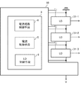
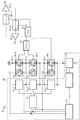
- FIG. 1 shows a laser diode driving apparatus 10 according to an outline of an embodiment of the present invention.
- the laser diode driving device 10 is a laser diode driving circuit that drives a plurality of laser diodes 31 connected in series between two power sources.
- FIG. 1 shows an example in which a plurality of laser diodes 31 are constituted by three laser diodes 31-1 to 31-3.
- the laser diode driving apparatus 10 includes driving means 3 that controls driving of a predetermined laser diode in accordance with the output state of the plurality of laser diodes 31.
- the laser diodes 31-1 and 31-2 are driven as working LDs
- the laser diode 31-3 is a predetermined laser diode (LD: Laser Diode).
- the predetermined laser diode is a spare LD that is used in place of the LD that cannot be used when any of the current LDs cannot be used due to a failure or the like.
- the predetermined laser diode is included in the plurality of laser diodes 31.
- the driving means 3 includes a current path control means 4, a current control means 5, and a laser diode control means 6 (LD control means 6 in FIG. 1).
- the current path control means 4 receives a signal corresponding to the output of each laser diode as input, and controls the current control means 5 according to the input signal.
- the current control means 5 receives a signal corresponding to the output of each laser diode, and controls the current supplied to each laser diode in accordance with the input signal.
- Laser diode control means 6 receives a signal corresponding to the output of each laser diode as input, and controls the current supplied between the two power supplies.
- the laser diode driving apparatus 10 According to the laser diode driving apparatus 10 according to the present embodiment described above, there is no change in the overall excitation laser diode intensity even when the excitation laser diode is switched. Therefore, in the optical direct amplification device using the laser diode driving device according to the present embodiment, the output does not change even when the excitation laser diode is switched.
- the laser diode driving device 10 according to the present embodiment will be described in more detail below.
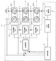
- the excitation LD drive circuit 10 includes a logic circuit 11, a bypass current control element 12 (12-1, 12-2, 12-3), an adder circuit 13, and an APC.
- the control part 14 and the LD drive part 15 are provided (APC: Automatic Power Control).
- the logic circuit 11 in FIG. 2 corresponds to the current path control means 4 in FIG.
- the current control element 12 in FIG. 2 corresponds to the current control means 5 in FIG.
- the adding circuit 13, the APC control unit 14, and the LD driving unit 15 in FIG. 2 are included in the driving unit 3 in FIG.
- the addition circuit 13 is also called addition means
- the APC control unit 14 is also called output control means
- the LD drive unit 15 is also called laser diode drive means.
- the excitation LD drive circuit 10 includes an excitation LD 31 (31-1, 31-2, 31-3) and a built-in PD 32 (32-1, 32-2, 32-3).
- the outputs of a plurality of pumping LD modules 30 (30-1, 30-2, 30-3) having (PD) are controlled (PD: Photodiode).
- the light output of the plurality of excitation LDs 31 is converted into a current value by the built-in PD 32 provided for each excitation LD 31.
- the output (signal) from each built-in PD 32 corresponds to the optical output of the corresponding excitation LD 31, and the total value of these outputs (signals) is the sum of the optical outputs from the plurality of excitation LD modules 30 (both the total output). Can be monitored).
- the optical outputs of the plurality of excitation LDs 31 may be detected not by a method of detecting a signal converted into a current value by the built-in PD 32 but by another method.
- the pumping LD modules 30-1 and 30-2 are used as active and the pumping LD module 30-3 is used as a backup.
- the configuration of the three-stage excitation LD 31 is illustrated, but it may be configured with four or more stages of excitation LD 31, or may be configured with two-stage excitation LD 31. May be.
- the logic circuit 11 receives outputs from the three built-in PDs 32 as inputs.
- the logic circuit 11 is connected to a plurality of bypass current control elements 12 connected in the subsequent stage, and controls the bypass current control elements 12.
- the logic circuit 11 is a current path control unit that takes the output of each excitation LD 31 as an input and controls the operation of each excitation LD 31 according to the output of each excitation LD 31.
- the logic circuit 11 controls the current value bypassed to the bypass current control element 12 with the use of the excitation LD 31. For example, when the output of the excitation LD 31 is sufficient, the current value bypassed to the bypass current control element 12 is increased, and when the output of the excitation LD 31 is insufficient, the current value bypassed to the bypass current control element 12 is increased. What is necessary is just to set so that it may become small. Note that the current value bypassed when the current excitation LD 31 is being driven is generally smaller than the current value bypassed to stop the spare excitation LD 31.
- the logic circuit 11 bypasses the bypass current control element 12 connected in parallel to the spare excitation LD 31. -3 is controlled.
- the current bypassed by the bypass current control element 12-3 is supplied to the spare excitation LD 31 by the control of the logic circuit 11.
- the spare excitation LD 31 emits light.
- the logic circuit 11 controls the bypass current control element 12 (12-1 or 12-2) connected in parallel to the excitation LD 31 (31-1 or 31-2) whose output is reduced.
- the bypass current control element 12 connected in parallel to the excitation LD 31 whose output is reduced bypasses the current supplied to the excitation LD 31 whose output is reduced, and the current excitation LD 31 whose output is reduced is stopped. To do.
- the logic circuit 11 executes drive control of the preliminary excitation LD 31-3 and stop control of the excitation LD 31 whose output is reduced. Note that the drive control and stop control by the logic circuit 11 may be executed sequentially or simultaneously.
- the bypass current control elements 12 (12-1, 12-2, 12-3) are connected to the plurality of pumping LD modules 30 (30-1, 30-2, 30-3) in parallel. It is an element.
- the bypass current control element 12 is installed at the subsequent stage of the logic circuit 10 and bypasses the current according to the output of the corresponding excitation LD 31.
- the bypass current control elements 12 (12-1, 12-2) operate according to the control from the logic circuit 11 when the output of the current excitation LD module 30 (30-1, 30-2) decreases. To do.
- the bypass current control element 12-3 connected to the spare excitation LD module 30-3 bypasses the current, and the excitation LD 31-3 is stopped. Electric power can be suppressed.
- the bypass current control element 12 When the bypass current control element 12 performs a bypass operation, the current supplied to the corresponding excitation LD module 30 is diverted to the bypass current control element 12. In other words, the bypass current control element 12 bypasses the current corresponding to the excitation LD 31 or the spare excitation LD 31-3 whose output has decreased. As a result, the excitation LD module 30 that is OFF does not generate a voltage drop due to the excitation LD 31, and is driven with the voltage distribution of two always operating. Therefore, compared with a pumping LD module having a configuration in which the pumping LD module 30-3 as a spare is not provided, the voltage distribution is the same as that in the general configuration, although one pumping LD is added in series. It is possible to control with.
- bypass current control element 12 performs a bypass operation, a small amount of current is assumed to flow through the corresponding excitation LD 31, but there is a problem if the bypassed excitation LD 31 does not emit light. Absent. Further, in the laser diode driving apparatus 10 of the present embodiment, a switch or a circuit that cuts off a very small amount of current flowing into the excitation LD 31 that is bypassed may be configured.
- the addition circuit 13 is addition means for inputting a signal obtained by converting the optical output of the excitation LD 31 into an electrical signal by the built-in PD 32.
- the signal input to the adder circuit 13 is the same as the signal input to the logic circuit 11.
- the adder circuit 13 receives the outputs from the built-in PDs 32 of the three excitation LD modules 30, calculates the total output (total output) of those outputs, and outputs a signal related to the total output to the APC control unit 14.
- the APC control unit 14 is an output control unit of the excitation LD module 30 and is an output control unit that controls the LD driving unit 15 in accordance with a signal from the addition circuit 13. Normally, a signal relating to the total output (total output value) of all the excitation LD modules 30 is input from the adder circuit 13. The APC control unit 14 controls the LD driving unit 15 so that the total output of the excitation LD module 30 is constant.
- the LD driving unit 15 is a laser diode driving unit that controls the pumping LD 31 included in the pumping LD module 30 according to a control signal from the APC control unit 14 so that the total output from the pumping LD module 30 is constant. It is.
- the LD driving unit 15 is connected in series with a three-stage excitation LD 31 between two power sources as shown in FIG.
- the LD driving unit 15 side (lower part) is set to the voltage V
- the excitation LD 31-1 side (upper part) is grounded (0 V).
- the power supply terminal and the ground terminal of the voltage V are called power supplies
- the power supply terminal and the ground terminal of the voltage V are called between power supplies.
- the LD drive unit 15 drives the current excitation LDs 31-1 and 31-2.
- the spare excitation LD 31-3 is not driven because the current is bypassed by the current control element 15-3 connected in parallel. Even if the spare excitation LD 31-3 is not driven, a current may flow through the excitation LD 31-3 as long as the excitation LD 31-3 does not emit light.
- the spare excitation LD 31-3 is driven.
- the LD driving unit 15 does not need to perform an operation of switching any of the excitation LDs 31-1 and 31-2 to the excitation LD 31-3, and in response to a control signal from the APC control unit 14, What is necessary is just to continue performing the control which drives LD31.
- the present invention is not limited to the above-described configuration.
- the circuit is configured to monitor the optical output of the pumping LD 31, detect a decrease in the output of the pumping LD 31 based on the variation of the monitored light output value, and operate the spare pumping LD 31, the present invention It is included in the range.
- the excitation LD drive circuit 10 In the excitation LD drive circuit 10 according to the present embodiment, two (30-1 and 30-2) of the three excitation LD modules 30 are driven as active. Further, it is assumed that the spare excitation LD module 30-3 is not driven in the initial state.
- the output of the built-in PD 32 of each excitation LD module 30 is subjected to current / voltage conversion and output to the adder circuit 13.
- the APC control unit 14 controls the LD drive unit 15 so that the total output of the two excitation LDs 31-1 and 31-2 calculated by the adder circuit 13 is constant (step S11).
- the logic circuit 11 When the current excitation LD 31 (31-1 or 31-2) fails and the output decreases (Yes in step S12), the logic circuit 11 is configured so that the spare excitation LD 31-3 is driven.
- the bypass current control element 12-3 is controlled (step S13). Specifically, the logic circuit 11 controls the current value bypassed by the bypass current control element 12-3 to be small, and a current sufficient for the excitation LD 31-3 to emit light is generated. -3.
- the APC control unit 14 performs control so that the total output of the excitation LD module 30 is constant.
- the logic circuit 11 performs control to operate the bypass current control element 12 (12-1 or 12-2) connected in parallel to the failed excitation LD 31 (31-1 or 31-2) (step S1). S14). Specifically, the logic circuit 11 performs control to increase the current value bypassed to the bypass current control element 12 connected in parallel to the failed excitation LD 31. At this time, the current supplied to the failed excitation LD 31 is bypassed by the bypass current control element 12, and the failed excitation LD 31 stops. As a result, even if any one of the current excitation LDs 31 fails, the total output of the excitation LD 31 is controlled to be constant.
- the excitation LD drive circuit As described above, in the excitation LD drive circuit according to the first embodiment of the present invention, when the current excitation LD fails, the spare excitation LD is started and the failed excitation LD is stopped. Thus, the output of the optical direct amplifier is not changed. As a result, it is possible to improve the reliability of the optical direct amplifying device equipped with the pumping LD drive circuit according to the present embodiment, and further the optical signal transmission system provided with the optical direct amplifying device.
- the excitation LD drive circuit according to the first embodiment of the present invention is particularly useful as an excitation LD drive circuit for an optical direct amplifying apparatus installed in a submarine cable system or the like that is difficult to repair after installation. is there.
- the optical direct amplifying apparatus 1 includes an LD driving circuit 10, a pumping LD module 30, a polarization combining coupler 40, a 3 dB coupler 50, a WDM coupler 60, and an optical amplifier 70 (WDM: Wavelength Division Multiplexing).
- excitation LD drive circuit 10 and the excitation LD module 30 are the same as those in the first embodiment, description thereof is omitted.
- the polarization beam combiner 40 receives the optical output from the current pumping LD 31 and multiplexes the input optical outputs.
- the optical signal combined by the polarization beam combiner 40 is output to the 3 dB coupler 50.
- the combined output of the polarization combining coupler 40 is half, that is, one pumping LD 31.
- the 3 dB coupler 50 is a branching coupler that branches the optical output combined by the polarization beam combining coupler 40 toward the upstream / downstream transmission path.
- Each of the optical signals branched by the 3 dB coupler 50 has an intensity equivalent to one excitation LD 31.
- the WDM couplers 60-1 and 60-2 each output an optical signal having the intensity of one excitation LD 31.
- the 3 dB coupler 50 When one of the current pumping LDs 31 fails, the 3 dB coupler 50 also receives the optical output from the spare pumping LD 31-3. Therefore, as in the case where the current pumping LD 31 is not out of order, an optical signal having an intensity equivalent to one pumping LD 31 is output to each of the WDM couplers 60-1 and 60-2.
- the WDM couplers 60 are wavelength division multiplexing couplers that input the optical output of the 3 dB coupler 50, combine and demultiplex, and output the demultiplexed light to the optical amplifier 70. .
- the optical amplifiers 70 are optical direct amplifiers that receive the optical signal from the WDM coupler 60 and output the optical signal in the upstream / downstream transmission path.
- the optical amplifier 70 an optical fiber in which rare earth ions such as trivalent erbium are added to quartz fiber can be used.
- the output of the optical amplifier 70 does not decrease. For this reason, the excitation LD intensity input to the optical amplifier 70 is always equal to the output of one excitation LD 31.
- the above is the description of the configuration of the optical direct amplification device 1 according to the second embodiment of the present invention.
- the configuration of the embodiment shown in FIG. 4 is an example, and does not limit the scope of the present invention.
- the output of the built-in PD 32 of each excitation LD module 30 is subjected to current / voltage conversion and output to the adder circuit 13.
- the APC control unit 14 controls the LD driving unit 15 in the adding circuit 13 so that the total output of the two excitation LDs 31-1 and 31-2 is constant (step S21).
- the polarization beam combiner 40 multiplexes the optical outputs of the pumping LDs 31-1 and 31-2. This is output to the 3 dB coupler 50 (step S23).
- the 3 dB coupler 50 receives the optical output of the polarization beam combining coupler 40, and outputs an optical signal branched toward the upstream / downstream transmission path via the WDM coupler 60 and the optical amplifier 70 (step S24).
- the logic circuit 11 drives the spare pumping LD 31-3.
- the bypass control element 12-3 is controlled (step S25). That is, the logic circuit 11 performs control to reduce the current value bypassed to the bypass control element 12-3 and to supply the excitation LD 31-3 with a current sufficient for the excitation LD 31-3 to emit light. I do.
- the APC control unit 14 performs control so that the total output of the excitation LD module 30 is constant.
- Step S26 the logic circuit 11 performs control to bypass current to the bypass current control element 12 (12-1 or 12-2) connected in parallel to the failed excitation LD 31 (31-1 or 31-2).
- Step S26 the logic circuit 11 performs control such that current is bypassed to the bypass current control element 12.
- the malfunctioning excitation LD 31 stops operating.
- steps S25 and S26 controls the total output of the excitation LD 31 to be constant even when any one of the current excitation LDs 31 breaks down.
- the polarization beam combiner 40 receives the optical output from the pumping LD 31 that is not out of the current pumping LDs 31, and multiplexes / demultiplexes the input optical output (step S27).
- the 3 dB coupler 50 receives the optical output of the polarization combining coupler 40 and also receives the optical output of the spare excitation LD 31-3, and multiplexes / demultiplexes the two optical outputs (step S28).
- the 3 dB coupler 50 outputs an optical signal toward the upstream / downstream transmission path via the WDM coupler 60 and the optical amplifier 70 (step S29).
- the optical output of the pumping LD 31 is multiplexed by the polarization beam combining coupler 40 and then the up / down signal is output by the 3 dB coupler 50. It is demultiplexed toward the transmission line.
- the excitation LD intensity input to the optical amplifier 70 of each transmission line is equal to the output of one excitation LD 31.
- the output of the optical amplifier 70 does not decrease even when the current pumping LD 31 fails.
- the excitation LD drive circuit 101 in FIG. 6 is configured to mount and drive only the current excitation LD 31 (31-1, 31-2).
- the excitation LD drive circuit 101 includes a constant current source unit 110, two APC control units 114 (114-1, 114-2), and two LD drive units 115 (115-1, 115-2). I have.
- the constant current source unit 110 is connected in series with the excitation LD 31 (31-1, 31-2) and supplies a constant current to the excitation LD 31.
- the APC control unit 114 (114-1, 114-2) detects the optical output of the excitation LD 31 (31-1, 31-2) included in each excitation LD module 30 (30-1, 30-2).
- the output of the built-in PD 32 (32-1, 32-2) is input.
- the APC control unit 114 controls the LD driving unit 115 according to the output of the built-in PD 32.
- the LD driving unit 115 drives the excitation LD 31 in accordance with the control of each APC control unit 114.
- the 3 dB coupler 50 combines the optical outputs of the pumping LDs 31 and outputs optical signals to the WDM couplers 60 (60-1 and 60-2) in the upstream / downstream transmission path.
- the WDM coupler 60 receives the output of the WDM coupler 60 (60-1, 60-2) and outputs it to the optical amplifier 70 (70-1, 70-2).
- the optical amplifier 70 receives the output of the WDM coupler 60 (60-1, 60-2), amplifies it, and then outputs the amplified optical signal to the upstream / downstream transmission path.
- the total pumping LD intensity is halved. That is, since the optical output input to the 3 dB coupler 50 is reduced, the output of the optical amplifier 70 is reduced.
- the output drop due to the failure mode is recovered after several relays. Therefore, even if one of the excitation LDs fails, there is no major problem in the system.
- the constant pumping light intensity control method it is necessary to use a highly reliable pumping LD, and there is a problem that the cost of the transmission line system including the optical direct amplifying device increases.
- the optical direct amplifying device using the excitation LD drive circuit according to the present embodiment even if a general excitation LD is used, if the excitation LD fails, a spare excitation LD Therefore, the output of the optical direct amplifying device does not decrease.
- a general excitation LD drive circuit it is necessary to provide an LD drive circuit for each excitation LD.
- an operation is performed with a single LD drive circuit. It becomes possible to make it. That is, according to the embodiment of the present invention, the configuration of the circuit / device is simplified as compared with a general excitation LD drive circuit.
- the excitation LD drive circuit 20 according to the third embodiment has basically the same configuration as the excitation LD drive circuit 10 according to the first embodiment. The difference is that, in addition to the current excitation LD 31 (31-1, 31-2), an LD module including a plurality of spare excitation LDs 31 (31-n) is controlled. Since other points are the same as those in the first embodiment, detailed description thereof is omitted.
- the logic circuit 11 selects any of the spare excitation LDs 31-n and selects the spare excitation LD 31-n selected in the same manner as in the first embodiment.
- the bypass current control element 12 is controlled so as to be driven.
- the logic circuit 11 is illustrated so that only the bypass current control element 12-n among the bypass current control elements 12 connected to the plurality of spare excitation LD modules 30 is connected. Actually, the bypass current control elements 12 connected to all the spare excitation LD modules 30 are connected to the logic circuit 11.
- the driven spare excitation LD 31-n operates as a new working excitation LD 31 together with the working excitation LD 31 that has not failed. Therefore, when one of the new working excitation LDs 31 in operation fails, another spare excitation LD 31-n can be driven.
- the excitation LD drive circuit 20 since a plurality of spare excitation LDs 31-n are mounted, the reliability of the system is further increased.
- An optical direct amplifying device 2 includes a pumping LD drive circuit 20, a pumping LD module 30, a polarization beam combining coupler 40, a 3 dB coupler 50, and the like according to the third embodiment.
- a WDM coupler 60 and an optical amplifier 70 are provided.
- the configurations other than the excitation LD drive circuit 20 and the excitation LD module 30 (30-1, 30-2,..., 30-n,...) Are the same as those in the second embodiment. Detailed description of the same configuration and operation is omitted.
- the input to the 3 dB coupler 50 is illustrated as being connected only to the spare excitation LD 31-n, but in reality, it is connected to all the spare excitation LDs 31. Yes.
- the spare pumping LD 31 is used. -N is driven. Since the optical output from the spare pumping LD 31-n is input to the 3 dB coupler 50, the output of the optical amplifier 70 does not decrease as in the second embodiment.
- the optical direct amplifying device 2 according to the fourth embodiment after the pumping LD 31 once fails, the spare pumping LD 31 is driven even if another pumping LD 31 fails again. As a result, the output of the optical amplifier 70 can be made constant. Therefore, the reliability of the entire optical signal transmission system using the optical direct amplification device 2 according to the present embodiment can be improved.
- An optical signal transmission system 200 includes an optical direct amplification device 201, an optical transmission device 202, an optical reception device 203, and a transmission path 204.
- the optical direct amplifying device 201 has the same configuration and function as the optical direct amplifying device 1 or 2 according to the second or fourth embodiment.
- the optical direct amplifying device 201 is included in an optical repeater or the like. Also good.
- FIG. 9 only the configuration necessary for the optical signal transmission system 200 according to the present embodiment is illustrated, and thus specific devices and devices that are actually configured as an optical communication system are omitted. .
- the optical transmitter 202 is connected to an external communication network such as the Internet, converts an electrical signal input from the communication network into an optical signal, and outputs the converted optical signal to the transmission line 204 toward the optical receiver 203.
- an external communication network such as the Internet
- the optical receiver 203 receives an optical signal from the transmission path 204, converts the received optical signal into an electrical signal, and outputs the electrical signal to an external communication network.
- the transmission line 204 is laid between the optical transmitter 202 and the optical receiver 203 and propagates an optical signal.
- the transmission path 204 is composed of an optical fiber whose main component is, for example, quartz.
- the optical fiber may be made of plastic.
- an optical fiber is laid by being covered with a protective member containing plastic or metal.
- the optical direct amplifier 201 is installed on the transmission line 204 and compensates for the waveform of the optical signal lost in the transmission line 204.
- a plurality of optical direct amplifiers 201 may be installed on the transmission line 204. Further, it is more preferable to insert isolators before and after the optical direct amplifier 200 because an optical signal traveling backward in the transmission path 204 can be removed.
- the optical signal transmission system 200 configured as described above, when the pumping LD 31 inside the optical direct amplifying device 201 fails, the faulty pumping LD31 is bypassed and the spare pumping LD31 is driven. A constant light output can be obtained stably.
- the optical signal transmission system 200 of this embodiment even if it is difficult to directly repair the pumping LD 31 that has failed after the transmission line 204 is laid, such as a submarine cable system, the pumping LD 31 is self-healing. Is done. Therefore, by applying the optical signal transmission system 200 of this embodiment, a highly reliable system can be configured. Further, the optical signal transmission system 200 of the present embodiment does not need to use a highly reliable pumping LD used in a pumping light intensity constant control method or the like, as compared with a general optical signal transmission system. It becomes possible to reduce the apparatus cost.
- the spare excitation LD when the excitation LD fails, the spare excitation LD is activated. As a result, there is no change in the total intensity of the excitation LD, and as a result, the first effect that the output from the optical direct amplification device does not change is obtained.
- the current excitation LD it is possible to drive the current excitation LD with a voltage distribution of two stages while the current excitation LD is in operation, despite the configuration in which the excitation LD is connected in series in three stages.
- the voltage distribution used in the LD driving circuit having a general configuration can be used as it is.
- the reliability of the apparatus is increased by mounting the spare excitation LD, it is possible to set a high failure rate to be allocated to the excitation LD module. As a result, it is possible to obtain a third effect that the purchase price of the pumping LD can be reduced, and the apparatus / system price of the optical direct amplifier and the optical signal transmission system can be reduced.
Landscapes
- Physics & Mathematics (AREA)
- Electromagnetism (AREA)
- Engineering & Computer Science (AREA)
- Computer Networks & Wireless Communication (AREA)
- Signal Processing (AREA)
- Condensed Matter Physics & Semiconductors (AREA)
- General Physics & Mathematics (AREA)
- Optics & Photonics (AREA)
- Lasers (AREA)
Abstract
In order to prevent the overall excitation laser diode intensity from changing when any of a plurality of in-use excitation laser diodes is switched to a spare excitation laser diode, the present invention provides a laser diode driver which is provided with a driving means which, in response to the output state of a plurality of laser diodes connected in series between two power sources, controls the driving of a prescribed laser diode. The driving means includes a current control means taking as an input a signal corresponding to the output of an individual laser diode and controlling the current supplied to the individual laser diode in response to the input signal, a current path control means for controlling the current control means in response to the input signal, and a laser diode control means for controlling the current supplied between the power sources in response to the input signal.
Description
本発明は、レーザーダイオード駆動装置、光直接増幅装置、光信号伝送システム及びレーザーダイオード駆動方法に関する。特に、海底ケーブルシステムなどの長距離光信号伝送システムで使用される光直接増幅装置のレーザーダイオード駆動装置に関する。
The present invention relates to a laser diode driving device, an optical direct amplification device, an optical signal transmission system, and a laser diode driving method. In particular, the present invention relates to a laser diode driving device for an optical direct amplifier used in a long-distance optical signal transmission system such as a submarine cable system.
海底などに敷設される長距離光信号伝送システムで使用される光直接増幅装置には、複数の励起用レーザーダイオード(以下、LD)が搭載されている(LD:Laser Diode)。一般的な光直接増幅装置は、現用の励起用LDのみを搭載・駆動する構成をとる。そのため、一部の励起用LDが故障した際には、トータルの励起LD強度が小さくなり、光直接増幅装置の出力が下がるという課題があった。
2. Description of the Related Art A plurality of pumping laser diodes (hereinafter referred to as LDs) are mounted on an optical direct amplifier used in a long-distance optical signal transmission system laid on the seabed (LD: Laser Diode). A general optical direct amplifying apparatus has a configuration in which only the current pumping LD is mounted and driven. For this reason, when some of the pumping LDs fail, there is a problem that the total pumping LD intensity decreases and the output of the optical direct amplifier decreases.
特許文献1には、LDの光出力が予め定められた値以下の場合、光出力が低くなったLDを迂回してバイアス電流を流す制御をするレーザーダイオード駆動回路について開示されている。
Patent Document 1 discloses a laser diode drive circuit that controls the flow of a bias current bypassing an LD whose light output is low when the light output of the LD is equal to or less than a predetermined value.
特許文献2には、光ファイバー中へ信号光と共に入力して光増幅するポンピング光の光源を複数個設け、劣化した動作中の光源を待機中の光源に交代させる光増幅用ポンピング光源の駆動方法について開示されている。
Patent Document 2 discloses a method for driving a pumping light source for optical amplification, in which a plurality of light sources for pumping light that are input into an optical fiber together with signal light to amplify the light are provided, and a deteriorated operating light source is replaced with a standby light source. It is disclosed.
一般的な構成の光直接増幅装置においては、励起光強度一定制御方式を採用すれば、搭載された一部のLDが故障したとしても、出力低下は数中継後に回復することが可能となる。しかしながら、励起光強度一定制御方式を用いる場合、信頼性の高い励起用LDを使用する必要があるため、装置コストが高くなるという課題があった。
In a direct optical amplifying apparatus having a general configuration, if a constant pumping light intensity control method is employed, even if some of the mounted LDs fail, the output drop can be recovered after several relays. However, in the case of using the excitation light intensity constant control method, it is necessary to use a highly reliable excitation LD, and there is a problem that the apparatus cost increases.
特許文献1のレーザーダイオード駆動回路では、複数のレーザーダイオードを個別にモニターする必要があるため、内部回路構成が複雑になるという課題があった。
In the laser diode drive circuit of Patent Document 1, it is necessary to individually monitor a plurality of laser diodes, which causes a problem that the internal circuit configuration is complicated.
特許文献2の光増幅用ポンピング光源では、劣化した光源を待機中の光源に交代する際に、総合的な光出力が変化するという課題があった。
The pumping light source for optical amplification of Patent Document 2 has a problem that the total light output changes when the deteriorated light source is replaced with a light source on standby.
本発明は、現用の励起用レーザーダイオードのいずれかを予備の励起用レーザーダイオードに切り替える場合であっても、総合的な励起レーザーダイオード強度に変化がないレーザーダイオード駆動装置を提供することを目的とする。
It is an object of the present invention to provide a laser diode drive device in which the overall pump laser diode intensity does not change even when any of the current pump laser diodes is switched to a spare pump laser diode. To do.
本発明のレーザーダイオード駆動装置は、2つの電源間に直列に接続された複数のレーザーダイオードの出力状態に応じて、所定のレーザーダイオードに対して駆動の制御をする駆動手段を備える。
The laser diode driving device of the present invention includes driving means for controlling driving of a predetermined laser diode according to the output state of a plurality of laser diodes connected in series between two power supplies.
本発明のレーザーダイオード駆動方法は、2つの電源間に直列に接続された複数のレーザーダイオードの出力状態に応じて、所定のレーザーダイオードに対して駆動の制御をする。
The laser diode driving method of the present invention controls driving of a predetermined laser diode according to the output state of a plurality of laser diodes connected in series between two power supplies.
本発明によれば、現用の励起用レーザーダイオードのいずれかを予備の励起用レーザーダイオードに切り替える場合であっても、総合的な励起レーザーダイオード強度に変化がないレーザーダイオード駆動装置を提供することができる。
According to the present invention, it is possible to provide a laser diode driving device in which the overall excitation laser diode intensity does not change even when any of the current excitation laser diodes is switched to a spare excitation laser diode. it can.
以下に、本発明を実施するための形態について図面を用いて説明する。但し、以下に述べる実施形態には、本発明を実施するために技術的に好ましい限定がされているが、発明の範囲を以下に限定するものではない。
Hereinafter, embodiments for carrying out the present invention will be described with reference to the drawings. However, the preferred embodiments described below are technically preferable for carrying out the present invention, but the scope of the invention is not limited to the following.
まず、本発明の概要について説明する。図1は、本発明の実施形態の概要に係るレーザーダイオード駆動装置10である。
First, the outline of the present invention will be described. FIG. 1 shows a laser diode driving apparatus 10 according to an outline of an embodiment of the present invention.
本実施形態に係るレーザーダイオード駆動装置10は、2つの電源間に直列に接続された複数のレーザーダイオード31を駆動するレーザーダイオード駆動回路である。図1には、複数のレーザーダイオード31が3つのレーザーダイオード31-1~3によって構成される例を図示している。
The laser diode driving device 10 according to the present embodiment is a laser diode driving circuit that drives a plurality of laser diodes 31 connected in series between two power sources. FIG. 1 shows an example in which a plurality of laser diodes 31 are constituted by three laser diodes 31-1 to 31-3.
本実施形態に係るレーザーダイオード駆動装置10は、複数のレーザーダイオード31の出力状態に応じて、所定のレーザーダイオードに対して駆動の制御をする駆動手段3を備える。図1の例では、レーザーダイオード31-1および31-2を現用のLDとして駆動しており、レーザーダイオード31-3を所定のレーザーダイオードとする(LD:Laser Diode)。なお、所定のレーザーダイオードとは、現用のLDのいずれかが故障等の理由で使用できなくなった際に、使用できなくなったLDの替わりに用いる予備のLDである。所定のレーザーダイオードは、複数のレーザーダイオード31に含まれるものである。
The laser diode driving apparatus 10 according to the present embodiment includes driving means 3 that controls driving of a predetermined laser diode in accordance with the output state of the plurality of laser diodes 31. In the example of FIG. 1, the laser diodes 31-1 and 31-2 are driven as working LDs, and the laser diode 31-3 is a predetermined laser diode (LD: Laser Diode). The predetermined laser diode is a spare LD that is used in place of the LD that cannot be used when any of the current LDs cannot be used due to a failure or the like. The predetermined laser diode is included in the plurality of laser diodes 31.
駆動手段3は、電流経路制御手段4、電流制御手段5、レーザーダイオード制御手段6(図1のLD制御手段6)を備える。
The driving means 3 includes a current path control means 4, a current control means 5, and a laser diode control means 6 (LD control means 6 in FIG. 1).
電流経路制御手段4は、個々のレーザーダイオードの出力に相当する信号を入力とし、入力した信号に応じて電流制御手段5を制御する。
The current path control means 4 receives a signal corresponding to the output of each laser diode as input, and controls the current control means 5 according to the input signal.
電流制御手段5は、個々のレーザーダイオードの出力に相当する信号を入力とし、入力した信号に応じて個々のレーザーダイオードに供給される電流を制御する。
The current control means 5 receives a signal corresponding to the output of each laser diode, and controls the current supplied to each laser diode in accordance with the input signal.
レーザーダイオード制御手段6は、個々のレーザーダイオードの出力に相当する信号を入力とし、2つの電源間に供給される電流を制御する。
Laser diode control means 6 receives a signal corresponding to the output of each laser diode as input, and controls the current supplied between the two power supplies.
以上の本実施形態に係るレーザーダイオード駆動装置10によれば、励起用レーザーダイオードを切り替える場合であっても、総合的な励起レーザーダイオード強度に変化がない。そのため、本実施形態に係るレーザーダイオード駆動装置を用いた光直接増幅装置においては、励起用レーザーダイオードを切り替える場合であっても出力が変化しないことになる。
According to the laser diode driving apparatus 10 according to the present embodiment described above, there is no change in the overall excitation laser diode intensity even when the excitation laser diode is switched. Therefore, in the optical direct amplification device using the laser diode driving device according to the present embodiment, the output does not change even when the excitation laser diode is switched.
続いて、以下において、本実施形態に係るレーザーダイオード駆動装置10についてより具体的に説明する。
Subsequently, the laser diode driving device 10 according to the present embodiment will be described in more detail below.
(第1の実施形態)
次に、図2を用いて本発明の第1の実施形態に係る励起用LD駆動回路10の構成について説明する。なお、以下の説明においては、現用のLDを2つとし、予備のLDを1つとする例を示すが、現用のLDは1つ又は3つ以上であってもよく、予備のLDが複数あってもよい。また、本実施形態においては、現用のLDが出力低下(故障)した場合を想定しているが、必要に応じて現用のLDを予備のLDに切り替える場合にも適用できる。 (First embodiment)
Next, the configuration of the excitation LD drivecircuit 10 according to the first embodiment of the present invention will be described with reference to FIG. In the following description, an example is shown in which two working LDs are used and one spare LD is used. However, one or three or more working LDs may be used, and there are a plurality of spare LDs. May be. Further, in the present embodiment, it is assumed that the working LD has a reduced output (failure), but the present invention can also be applied to switching the working LD to a spare LD as necessary.
次に、図2を用いて本発明の第1の実施形態に係る励起用LD駆動回路10の構成について説明する。なお、以下の説明においては、現用のLDを2つとし、予備のLDを1つとする例を示すが、現用のLDは1つ又は3つ以上であってもよく、予備のLDが複数あってもよい。また、本実施形態においては、現用のLDが出力低下(故障)した場合を想定しているが、必要に応じて現用のLDを予備のLDに切り替える場合にも適用できる。 (First embodiment)
Next, the configuration of the excitation LD drive
本発明の第1の実施形態に係る励起用LD駆動回路10は、論理回路11と、バイパス用電流制御素子12(12-1、12-2、12-3)と、加算回路13と、APC制御部14と、LD駆動部15と、を備える(APC:Automatic Power Control)。
The excitation LD drive circuit 10 according to the first embodiment of the present invention includes a logic circuit 11, a bypass current control element 12 (12-1, 12-2, 12-3), an adder circuit 13, and an APC. The control part 14 and the LD drive part 15 are provided (APC: Automatic Power Control).
図2の論理回路11は、図1の電流経路制御手段4に相当する。図2の電流制御素子12は、図1の電流制御手段5に相当する。図2の加算回路13、APC制御部14およびLD駆動部15は、図1の駆動手段3に含まれる。なお、加算回路13は加算手段、APC制御部14は出力制御手段、LD駆動部15はレーザーダイオード駆動手段とも呼ぶ。
The logic circuit 11 in FIG. 2 corresponds to the current path control means 4 in FIG. The current control element 12 in FIG. 2 corresponds to the current control means 5 in FIG. The adding circuit 13, the APC control unit 14, and the LD driving unit 15 in FIG. 2 are included in the driving unit 3 in FIG. The addition circuit 13 is also called addition means, the APC control unit 14 is also called output control means, and the LD drive unit 15 is also called laser diode drive means.
本発明の第1の実施形態に係る励起用LD駆動回路10は、励起用LD31(31-1、31-2、31-3)及び内蔵PD32(32-1、32-2、32-3)を有する複数の励起LDモジュール30(30-1、30-2、30-3)の出力を制御する(PD:Photodiode)。
The excitation LD drive circuit 10 according to the first embodiment of the present invention includes an excitation LD 31 (31-1, 31-2, 31-3) and a built-in PD 32 (32-1, 32-2, 32-3). The outputs of a plurality of pumping LD modules 30 (30-1, 30-2, 30-3) having (PD) are controlled (PD: Photodiode).
図2を参照すると、複数の励起用LD31の光出力は、それぞれの励起用LD31に対して設けられた内蔵PD32によって電流値に変換される。それぞれの内蔵PD32からの出力(信号)は、対応する励起用LD31の光出力に相当し、それらの出力(信号)の合計値が複数の励起LDモジュール30からの光出力の総和(合計出力とも呼ぶ)としてモニターできる。なお、複数の励起用LD31の光出力は、内蔵PD32によって電流値に変換された信号を検出する方式ではなく、別の方式によって検出してもよい。
Referring to FIG. 2, the light output of the plurality of excitation LDs 31 is converted into a current value by the built-in PD 32 provided for each excitation LD 31. The output (signal) from each built-in PD 32 corresponds to the optical output of the corresponding excitation LD 31, and the total value of these outputs (signals) is the sum of the optical outputs from the plurality of excitation LD modules 30 (both the total output). Can be monitored). Note that the optical outputs of the plurality of excitation LDs 31 may be detected not by a method of detecting a signal converted into a current value by the built-in PD 32 but by another method.
なお、本実施形態においては、励起LDモジュール30-1及び30-2を現用とし、励起LDモジュール30-3を予備とすることを前提とする。また、本実施形態においては、3段の励起用LD31の構成について例示しているが、4段以上の励起用LD31で構成されていてもよく、また、2段の励起用LD31で構成されていてもよい。
In the present embodiment, it is assumed that the pumping LD modules 30-1 and 30-2 are used as active and the pumping LD module 30-3 is used as a backup. Further, in the present embodiment, the configuration of the three-stage excitation LD 31 is illustrated, but it may be configured with four or more stages of excitation LD 31, or may be configured with two-stage excitation LD 31. May be.
論理回路11は、3つの内蔵PD32からの出力を入力とする。論理回路11は、後段に接続されている複数のバイパス用電流制御素子12に接続され、バイパス用電流制御素子12を制御する。論理回路11は、それぞれの励起用LD31の出力を入力とし、それぞれ励起用LD31の出力に応じて、それぞれの励起用LD31の動作を制御する電流経路制御手段である。
The logic circuit 11 receives outputs from the three built-in PDs 32 as inputs. The logic circuit 11 is connected to a plurality of bypass current control elements 12 connected in the subsequent stage, and controls the bypass current control elements 12. The logic circuit 11 is a current path control unit that takes the output of each excitation LD 31 as an input and controls the operation of each excitation LD 31 according to the output of each excitation LD 31.
励起用LD31の出力低下は、徐々に起こることが一般的である。そのため、励起用LD31の使用に伴って、論理回路11は、バイパス用電流制御素子12にバイパスする電流値を制御する。例えば、励起用LD31の出力が十分な場合、バイパス用電流制御素子12にバイパスする電流値を大きくし、励起用LD31の出力が不十分な場合、バイパス用電流制御素子12にバイパスする電流値を小さくなるように設定すればよい。なお、現用の励起用LD31を駆動させている場合にバイパスする電流値は、予備の励起用LD31を停止させるためにバイパスする電流値と比較すると小さい値となるのが一般的である。
Generally, the output decrease of the excitation LD 31 gradually occurs. Therefore, the logic circuit 11 controls the current value bypassed to the bypass current control element 12 with the use of the excitation LD 31. For example, when the output of the excitation LD 31 is sufficient, the current value bypassed to the bypass current control element 12 is increased, and when the output of the excitation LD 31 is insufficient, the current value bypassed to the bypass current control element 12 is increased. What is necessary is just to set so that it may become small. Note that the current value bypassed when the current excitation LD 31 is being driven is generally smaller than the current value bypassed to stop the spare excitation LD 31.
論理回路11は、現用の励起用LD31(31-1又は31-2)のいずれかの出力が許容を超えて低下した場合、予備の励起用LD31に並列に接続されたバイパス用電流制御素子12-3を制御する。励起用LD31を切り替える場合、論理回路11の制御によって、バイパス用電流制御素子12-3にバイパスされていた電流が予備の励起用LD31に供給される。発光するために必要な電流が予備の励起用LD31に供給されると、予備の励起用LD31が発光する。
When the output of any of the current excitation LDs 31 (31-1 or 31-2) falls below an allowable level, the logic circuit 11 bypasses the bypass current control element 12 connected in parallel to the spare excitation LD 31. -3 is controlled. When switching the excitation LD 31, the current bypassed by the bypass current control element 12-3 is supplied to the spare excitation LD 31 by the control of the logic circuit 11. When the current necessary for light emission is supplied to the spare excitation LD 31, the spare excitation LD 31 emits light.
また、論理回路11は、出力が低下した励起用LD31(31-1又は31-2)に並列接続されているバイパス用電流制御素子12(12-1又は12-2)を制御する。出力が低下した励起用LD31に並列接続されているバイパス用電流制御素子12には、出力が低下した励起用LD31に供給されていた電流がバイパスされ、出力が低下した現用の励起用LD31は停止する。
Further, the logic circuit 11 controls the bypass current control element 12 (12-1 or 12-2) connected in parallel to the excitation LD 31 (31-1 or 31-2) whose output is reduced. The bypass current control element 12 connected in parallel to the excitation LD 31 whose output is reduced bypasses the current supplied to the excitation LD 31 whose output is reduced, and the current excitation LD 31 whose output is reduced is stopped. To do.
論理回路11によって、予備の励起用LD31-3の駆動制御と、出力が低下した励起用LD31の停止制御と、が実行される。なお、論理回路11による駆動制御及び停止制御は、順番に実行されてもよいし、同時に実行されてもよい。
The logic circuit 11 executes drive control of the preliminary excitation LD 31-3 and stop control of the excitation LD 31 whose output is reduced. Note that the drive control and stop control by the logic circuit 11 may be executed sequentially or simultaneously.
バイパス用電流制御素子12(12-1、12-2、12-3)は、複数の励起LDモジュール30(30-1、30-2、30-3)に対して並列に接続される電流制御素子である。バイパス用電流制御素子12は、論理回路10の後段に設置され、対応するそれぞれの励起用LD31の出力に応じて電流をバイパスする。
The bypass current control elements 12 (12-1, 12-2, 12-3) are connected to the plurality of pumping LD modules 30 (30-1, 30-2, 30-3) in parallel. It is an element. The bypass current control element 12 is installed at the subsequent stage of the logic circuit 10 and bypasses the current according to the output of the corresponding excitation LD 31.
バイパス用電流制御素子12(12-1、12-2)は、現用の励起LDモジュール30(30-1、30-2)の出力が低下した場合に、論理回路11からの制御に応じて動作する。通常時、予備となる励起LDモジュール30-3に接続されたバイパス用電流制御素子12-3に電流をバイパスさせ、励起用LD31-3を停止させておくため、励起LDモジュール30-3の消費電力を抑制できる。
The bypass current control elements 12 (12-1, 12-2) operate according to the control from the logic circuit 11 when the output of the current excitation LD module 30 (30-1, 30-2) decreases. To do. During normal operation, the bypass current control element 12-3 connected to the spare excitation LD module 30-3 bypasses the current, and the excitation LD 31-3 is stopped. Electric power can be suppressed.
バイパス用電流制御素子12がバイパス動作すると、対応する励起LDモジュール30に供給されていた電流は、バイパス用電流制御素子12に迂回される。すなわち、バイパス用電流制御素子12は、出力が低下した励起用LD31又は予備の励起用LD31-3に対応した電流をバイパスする。その結果、OFFとなっている励起LDモジュール30では励起用LD31による電圧降下が発生せず、常に動作している2つ分の電圧配分で駆動される。そのため、予備となる励起LDモジュール30-3を設けていない構成の励起LDモジュールと比べると、励起用LDを1段分直列に追加しているにもかかわらず、一般的な構成と同じ電圧配分で制御することが可能である。なお、バイパス用電流制御素子12がバイパス動作をしていても、対応する励起用LD31に微量の電流が流れることが想定されるが、バイパスされている励起用LD31が発光しない程度であれば問題ない。また、本実施形態のレーザーダイオード駆動装置10においては、バイパスされている励起用LD31に流れこむ微量な電流を遮断するスイッチや回路を構成させてもよい。
When the bypass current control element 12 performs a bypass operation, the current supplied to the corresponding excitation LD module 30 is diverted to the bypass current control element 12. In other words, the bypass current control element 12 bypasses the current corresponding to the excitation LD 31 or the spare excitation LD 31-3 whose output has decreased. As a result, the excitation LD module 30 that is OFF does not generate a voltage drop due to the excitation LD 31, and is driven with the voltage distribution of two always operating. Therefore, compared with a pumping LD module having a configuration in which the pumping LD module 30-3 as a spare is not provided, the voltage distribution is the same as that in the general configuration, although one pumping LD is added in series. It is possible to control with. Note that even if the bypass current control element 12 performs a bypass operation, a small amount of current is assumed to flow through the corresponding excitation LD 31, but there is a problem if the bypassed excitation LD 31 does not emit light. Absent. Further, in the laser diode driving apparatus 10 of the present embodiment, a switch or a circuit that cuts off a very small amount of current flowing into the excitation LD 31 that is bypassed may be configured.
加算回路13は、内蔵PD32が励起用LD31の光出力を電気信号に変換した信号を入力する加算手段である。加算回路13に入力する信号は、論理回路11に入力する信号と同じである。加算回路13は、3つの励起LDモジュール30の内蔵PD32からの出力を入力し、それらの出力を合計したトータル出力(合計出力)を計算し、トータル出力に関する信号をAPC制御部14に出力する。
The addition circuit 13 is addition means for inputting a signal obtained by converting the optical output of the excitation LD 31 into an electrical signal by the built-in PD 32. The signal input to the adder circuit 13 is the same as the signal input to the logic circuit 11. The adder circuit 13 receives the outputs from the built-in PDs 32 of the three excitation LD modules 30, calculates the total output (total output) of those outputs, and outputs a signal related to the total output to the APC control unit 14.
APC制御部14は、励起LDモジュール30の出力制御部であって、加算回路13からの信号に応じて、LD駆動部15を制御する出力制御手段である。通常、加算回路13からは、全ての励起LDモジュール30のトータル出力(出力の合計値)に関する信号を入力する。APC制御部14は、励起LDモジュール30のトータル出力が一定となるように、LD駆動部15を制御する。
The APC control unit 14 is an output control unit of the excitation LD module 30 and is an output control unit that controls the LD driving unit 15 in accordance with a signal from the addition circuit 13. Normally, a signal relating to the total output (total output value) of all the excitation LD modules 30 is input from the adder circuit 13. The APC control unit 14 controls the LD driving unit 15 so that the total output of the excitation LD module 30 is constant.
LD駆動部15は、APC制御部14からの制御信号に応じて、励起LDモジュール30に含まれる励起用LD31を、励起LDモジュール30からのトータル出力が一定となるように制御するレーザーダイオード駆動手段である。
The LD driving unit 15 is a laser diode driving unit that controls the pumping LD 31 included in the pumping LD module 30 according to a control signal from the APC control unit 14 so that the total output from the pumping LD module 30 is constant. It is.
LD駆動部15は、図2のように、2つの電源間において3段の励起用LD31と直列に接続される。図2に示した本実施形態においては、LD駆動部15側(下部)を電圧Vに設定し、励起用LD31-1側(上部)を接地(0V)するように図示している。本発明の実施形態においては、電圧Vの電源端と接地端とを電源とよび、電圧Vの電源端と接地端との間を電源間とよぶ。
The LD driving unit 15 is connected in series with a three-stage excitation LD 31 between two power sources as shown in FIG. In the present embodiment shown in FIG. 2, the LD driving unit 15 side (lower part) is set to the voltage V, and the excitation LD 31-1 side (upper part) is grounded (0 V). In the embodiment of the present invention, the power supply terminal and the ground terminal of the voltage V are called power supplies, and the power supply terminal and the ground terminal of the voltage V are called between power supplies.
通常時、LD駆動部15は、現用の励起用LD31-1及び31-2を駆動する。このとき、予備の励起用LD31-3は、並列に接続された電流制御素子15-3に電流をバイパスさせているために駆動されない。なお、予備の励起用LD31-3を駆動していなくても、励起用LD31-3の発光が起こらない程度の電流であれば、励起用LD31-3に電流が流れてもよい。
During normal operation, the LD drive unit 15 drives the current excitation LDs 31-1 and 31-2. At this time, the spare excitation LD 31-3 is not driven because the current is bypassed by the current control element 15-3 connected in parallel. Even if the spare excitation LD 31-3 is not driven, a current may flow through the excitation LD 31-3 as long as the excitation LD 31-3 does not emit light.
現用の励起用LD31-1及び31-2のいずれかの光出力が許容以下となった場合、予備の励起用LD31-3が駆動される。このとき、LD駆動部15は、励起用LD31-1及び31-2のいずれかを励起用LD31-3に切り替える動作をする必要はなく、APC制御部14からの制御信号に応じて、励起用LD31を駆動させる制御を実行し続ければよい。
When the light output of any of the current excitation LDs 31-1 and 31-2 falls below an allowable level, the spare excitation LD 31-3 is driven. At this time, the LD driving unit 15 does not need to perform an operation of switching any of the excitation LDs 31-1 and 31-2 to the excitation LD 31-3, and in response to a control signal from the APC control unit 14, What is necessary is just to continue performing the control which drives LD31.
以上が、本実施形態に係る励起LD駆動回路10の構成についての説明である。なお、本発明の範囲は、上述の構成に限定されない。励起用LD31の光出力をモニターし、モニターした光出力値の変動に基づいて励起用LD31の出力低下を検知し、予備の励起用LDを動作できる構成を持つ回路でありさえすれば、本発明の範囲に含まれるものである。
The above is the description of the configuration of the excitation LD drive circuit 10 according to the present embodiment. Note that the scope of the present invention is not limited to the above-described configuration. As long as the circuit is configured to monitor the optical output of the pumping LD 31, detect a decrease in the output of the pumping LD 31 based on the variation of the monitored light output value, and operate the spare pumping LD 31, the present invention It is included in the range.
(動作)
次に、図3を用いて、本発明の第1の実施形態に係る励起用LD駆動回路10の動作について説明する。 (Operation)
Next, the operation of the excitationLD drive circuit 10 according to the first embodiment of the present invention will be described with reference to FIG.
次に、図3を用いて、本発明の第1の実施形態に係る励起用LD駆動回路10の動作について説明する。 (Operation)
Next, the operation of the excitation
なお、本実施形態に係る励起用LD駆動回路10においては、3つの励起LDモジュール30のうち2つ(30-1、30-2)を現用として駆動するものとする。また、予備となる励起LDモジュール30-3は、初期状態では駆動されていないものとする。
In the excitation LD drive circuit 10 according to the present embodiment, two (30-1 and 30-2) of the three excitation LD modules 30 are driven as active. Further, it is assumed that the spare excitation LD module 30-3 is not driven in the initial state.
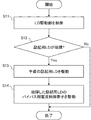
各励起LDモジュール30の内蔵PD32の出力は、電流/電圧変換され、加算回路13に向けて出力される。加算回路13によって計算される2つの励起用LD31-1及び31-2のトータル出力が一定となるように、APC制御部14は、LD駆動部15を制御する(ステップS11)。
The output of the built-in PD 32 of each excitation LD module 30 is subjected to current / voltage conversion and output to the adder circuit 13. The APC control unit 14 controls the LD drive unit 15 so that the total output of the two excitation LDs 31-1 and 31-2 calculated by the adder circuit 13 is constant (step S11).
現用のLD31(31-1及び31-2)が故障していない(出力が低下していない)場合(ステップS12でNo)、このフローは終了とする。
If the current LD 31 (31-1 and 31-2) has not failed (the output has not decreased) (No in step S12), this flow ends.
現用の励起用LD31(31-1又は31-2)が故障して出力が低下した場合(ステップS12でYes)、論理回路11は、予備となる励起用LD31-3が駆動されるように、バイパス用電流制御素子12-3を制御する(ステップS13)。具体的には、論理回路11は、バイパス用電流制御素子12-3にバイパスされていた電流値が小さくなるように制御し、励起用LD31-3が発光するのに十分な電流が励起用LD31-3に対して供給されるように制御する。このとき、APC制御部14は、励起LDモジュール30のトータル出力が一定になるように制御する。
When the current excitation LD 31 (31-1 or 31-2) fails and the output decreases (Yes in step S12), the logic circuit 11 is configured so that the spare excitation LD 31-3 is driven. The bypass current control element 12-3 is controlled (step S13). Specifically, the logic circuit 11 controls the current value bypassed by the bypass current control element 12-3 to be small, and a current sufficient for the excitation LD 31-3 to emit light is generated. -3. At this time, the APC control unit 14 performs control so that the total output of the excitation LD module 30 is constant.
そして、論理回路11は、故障した励起用LD31(31-1又は31-2)に並列接続されているバイパス用電流制御素子12(12-1又は12-2)を動作させる制御を行う(ステップS14)。具体的には、論理回路11は、故障した励起用LD31に並列に接続されたバイパス用電流制御素子12にバイパスする電流値を増大させる制御を行う。この際、故障した励起用LD31に供給されていた電流がバイパス用電流制御素子12にバイパスされ、故障した励起用LD31は停止する。その結果、現用の励起用LD31のいずれか1つが故障した場合であっても、励起用LD31のトータル出力は一定に制御される。
Then, the logic circuit 11 performs control to operate the bypass current control element 12 (12-1 or 12-2) connected in parallel to the failed excitation LD 31 (31-1 or 31-2) (step S1). S14). Specifically, the logic circuit 11 performs control to increase the current value bypassed to the bypass current control element 12 connected in parallel to the failed excitation LD 31. At this time, the current supplied to the failed excitation LD 31 is bypassed by the bypass current control element 12, and the failed excitation LD 31 stops. As a result, even if any one of the current excitation LDs 31 fails, the total output of the excitation LD 31 is controlled to be constant.
以上が、本実施形態に係る励起用LD駆動回路10の動作についての説明である。なお、本発明の範囲は、上述の動作に限定されない。励起用LDの光出力をモニターし、モニターした光出力値の変動に基づいて励起用LDの故障を検知し、予備の励起用LDを動作させるフローであれば、本発明の範囲に含まれるものである。
The above is the description of the operation of the excitation LD drive circuit 10 according to the present embodiment. The scope of the present invention is not limited to the above-described operation. Any flow that monitors the optical output of the excitation LD, detects a failure of the excitation LD based on the variation in the monitored optical output value, and operates the spare excitation LD is included in the scope of the present invention. It is.
以上のように、本発明の第1の実施形態に係る励起用LD駆動回路では、現用の励起用LDが故障した場合に予備の励起用LDを起動するとともに、故障した励起用LDを停止させることによって、光直接増幅装置の出力が変化しないことを特徴とする。その結果、本実施形態に係る励起用LD駆動回路を搭載した光直接増幅装置、さらにはその光直接増幅装置を設置した光信号伝送システムの信頼性を向上させることが可能となる。
As described above, in the excitation LD drive circuit according to the first embodiment of the present invention, when the current excitation LD fails, the spare excitation LD is started and the failed excitation LD is stopped. Thus, the output of the optical direct amplifier is not changed. As a result, it is possible to improve the reliability of the optical direct amplifying device equipped with the pumping LD drive circuit according to the present embodiment, and further the optical signal transmission system provided with the optical direct amplifying device.
本発明の第1の実施形態に係る励起用LD駆動回路は、特に、設置後に修理することが困難であるような海底ケーブルシステムなどに設置する光直接増幅装置の励起用LD駆動回路として有用である。
The excitation LD drive circuit according to the first embodiment of the present invention is particularly useful as an excitation LD drive circuit for an optical direct amplifying apparatus installed in a submarine cable system or the like that is difficult to repair after installation. is there.
(第2の実施形態)
次に、図4を用いて本発明の第2の実施形態に係る光直接増幅装置1について説明する。 (Second Embodiment)
Next, an optical direct amplification device 1 according to a second embodiment of the present invention will be described with reference to FIG.
次に、図4を用いて本発明の第2の実施形態に係る光直接増幅装置1について説明する。 (Second Embodiment)
Next, an optical direct amplification device 1 according to a second embodiment of the present invention will be described with reference to FIG.
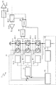
本実施形態に係る光直接増幅装置1は、LD駆動回路10、励起LDモジュール30、偏波合成カプラ40、3dBカプラ50、WDMカプラ60、光アンプ70を備える(WDM:Wavelength Division Multiplexing)。
The optical direct amplifying apparatus 1 according to the present embodiment includes an LD driving circuit 10, a pumping LD module 30, a polarization combining coupler 40, a 3 dB coupler 50, a WDM coupler 60, and an optical amplifier 70 (WDM: Wavelength Division Multiplexing).
励起用LD駆動回路10及び励起LDモジュール30は、第1の実施形態と同様であるため、説明は省略する。
Since the excitation LD drive circuit 10 and the excitation LD module 30 are the same as those in the first embodiment, description thereof is omitted.
偏波合成カプラ40は、現用の励起用LD31からの光出力を入力し、入力した光出力を合波する。偏波合成カプラ40によって合波された光信号は、3dBカプラ50に対して出力される。
The polarization beam combiner 40 receives the optical output from the current pumping LD 31 and multiplexes the input optical outputs. The optical signal combined by the polarization beam combiner 40 is output to the 3 dB coupler 50.
なお、現用の励起用LD31の一つが故障した場合、偏波合成カプラ40の合波出力は半分、すなわち励起用LD31一つ分となる。
When one of the current pumping LDs 31 breaks down, the combined output of the polarization combining coupler 40 is half, that is, one pumping LD 31.
3dBカプラ50は、偏波合成カプラ40によって合波された光出力を上り/下りの伝送路に向けて分岐する分岐カプラである。3dBカプラ50によって分岐された光信号は、それぞれ励起用LD31一個分の強度となる。すなわち、WDMカプラ60-1及び60-2に対しては、それぞれ励起用LD31一個分の強度の光信号が出力される。
The 3 dB coupler 50 is a branching coupler that branches the optical output combined by the polarization beam combining coupler 40 toward the upstream / downstream transmission path. Each of the optical signals branched by the 3 dB coupler 50 has an intensity equivalent to one excitation LD 31. In other words, the WDM couplers 60-1 and 60-2 each output an optical signal having the intensity of one excitation LD 31.
なお、現用の励起用LD31の一つが故障した場合、3dBカプラ50には、予備の励起用LD31-3からの光出力も入力される。そのため、現用の励起用LD31が故障していない場合と同様に、WDMカプラ60-1及び60-2に対しては、それぞれ励起用LD31一個分の強度の光信号が出力される。
When one of the current pumping LDs 31 fails, the 3 dB coupler 50 also receives the optical output from the spare pumping LD 31-3. Therefore, as in the case where the current pumping LD 31 is not out of order, an optical signal having an intensity equivalent to one pumping LD 31 is output to each of the WDM couplers 60-1 and 60-2.
WDMカプラ60(60-1、60-2)は、3dBカプラ50の光出力を入力して合・分波し、光アンプ70に対して分波した光を出力する波長分割多重方式カプラである。
The WDM couplers 60 (60-1 and 60-2) are wavelength division multiplexing couplers that input the optical output of the 3 dB coupler 50, combine and demultiplex, and output the demultiplexed light to the optical amplifier 70. .
光アンプ70(70-1、70-2)は、WDMカプラ60からの光信号を入力し、上り/下りの伝送路内に光信号を出力する光直接増幅器である。例えば、光アンプ70としては、石英ファイバーに3価のエルビウムなどの希土類イオンを添加した光ファイバーを用いることができる。
The optical amplifiers 70 (70-1 and 70-2) are optical direct amplifiers that receive the optical signal from the WDM coupler 60 and output the optical signal in the upstream / downstream transmission path. For example, as the optical amplifier 70, an optical fiber in which rare earth ions such as trivalent erbium are added to quartz fiber can be used.
本実施形態によれば、現用の励起用LD31の一つが故障したとしても、光アンプ70の出力が低下することはない。そのため、光アンプ70へ入力される励起LD強度は、常に励起用LD31一個分の出力に等しくなる。
According to the present embodiment, even if one of the current pumping LDs 31 breaks down, the output of the optical amplifier 70 does not decrease. For this reason, the excitation LD intensity input to the optical amplifier 70 is always equal to the output of one excitation LD 31.
以上が、本発明の第2の実施形態に係る光直接増幅装置1の構成についての説明である。なお、図4に示した実施形態の構成は一例であって、本発明の範囲を限定するものではない。
The above is the description of the configuration of the optical direct amplification device 1 according to the second embodiment of the present invention. The configuration of the embodiment shown in FIG. 4 is an example, and does not limit the scope of the present invention.
(動作)
次に、図5を用いて、本発明の第2の実施形態に係る光直接増幅装置1の動作について説明する。なお、本実施形態においても、第1の実施形態と同様に、3つの励起LDモジュール30のうち2つ(30-1、30-2)を現用として駆動するものとする。また、予備となる励起LDモジュール30-3は、初期状態では駆動されていないものとする。 (Operation)
Next, the operation of the optical direct amplification device 1 according to the second embodiment of the present invention will be described with reference to FIG. In this embodiment as well, as in the first embodiment, two (30-1 and 30-2) of the threeexcitation LD modules 30 are driven as active. Further, it is assumed that the preliminary excitation LD module 30-3 is not driven in the initial state.
次に、図5を用いて、本発明の第2の実施形態に係る光直接増幅装置1の動作について説明する。なお、本実施形態においても、第1の実施形態と同様に、3つの励起LDモジュール30のうち2つ(30-1、30-2)を現用として駆動するものとする。また、予備となる励起LDモジュール30-3は、初期状態では駆動されていないものとする。 (Operation)
Next, the operation of the optical direct amplification device 1 according to the second embodiment of the present invention will be described with reference to FIG. In this embodiment as well, as in the first embodiment, two (30-1 and 30-2) of the three
各励起LDモジュール30の内蔵PD32の出力は、電流/電圧変換され、加算回路13に向けて出力される。APC制御部14は、加算回路13において2つの励起用LD31-1及び31-2のトータル出力が一定となるようにLD駆動部15を制御する(ステップS21)。
The output of the built-in PD 32 of each excitation LD module 30 is subjected to current / voltage conversion and output to the adder circuit 13. The APC control unit 14 controls the LD driving unit 15 in the adding circuit 13 so that the total output of the two excitation LDs 31-1 and 31-2 is constant (step S21).
まず、現用の励起用LD31が故障していない場合(ステップS22でNo)について説明する。
First, a case where the current excitation LD 31 has not failed (No in step S22) will be described.
現用の励起用LD31(31-1又は31-2)が故障していない場合(ステップS22でNo)、偏波合成カプラ40は、励起用LD31-1及び31-2の光出力を合波し、3dBカプラ50に出力する(ステップS23)。
If the current pumping LD 31 (31-1 or 31-2) has not failed (No in step S22), the polarization beam combiner 40 multiplexes the optical outputs of the pumping LDs 31-1 and 31-2. This is output to the 3 dB coupler 50 (step S23).
3dBカプラ50は、偏波合成カプラ40の光出力を入力し、WDMカプラ60・光アンプ70を介して、上り/下りの伝送路に向けて分岐させた光信号を出力する(ステップS24)。
The 3 dB coupler 50 receives the optical output of the polarization beam combining coupler 40, and outputs an optical signal branched toward the upstream / downstream transmission path via the WDM coupler 60 and the optical amplifier 70 (step S24).
次に、現用の励起用LD31-1又は31-2のいずれかが故障した場合(ステップS22でYes)について説明する。
Next, a case where either the current excitation LD 31-1 or 31-2 has failed (Yes in step S22) will be described.
一方、現用の励起用LD31(31-1又は31-2)が故障して出力が低下した場合(ステップS22でYes)、論理回路11は、予備となる励起用LD31-3を駆動するようにバイパス用制御素子12-3を制御する(ステップS25)。すなわち、論理回路11は、バイパス用制御素子12-3にバイパスしていた電流値を小さくし、励起用LD31-3が発光するのに十分な電流を励起用LD31-3に対して供給する制御を行う。このとき、APC制御部14は、励起LDモジュール30のトータル出力が一定になるように制御する。
On the other hand, when the current pumping LD 31 (31-1 or 31-2) fails and the output decreases (Yes in step S22), the logic circuit 11 drives the spare pumping LD 31-3. The bypass control element 12-3 is controlled (step S25). That is, the logic circuit 11 performs control to reduce the current value bypassed to the bypass control element 12-3 and to supply the excitation LD 31-3 with a current sufficient for the excitation LD 31-3 to emit light. I do. At this time, the APC control unit 14 performs control so that the total output of the excitation LD module 30 is constant.
そして、論理回路11は、故障した励起用LD31(31-1又は31-2)に並列接続されているバイパス用電流制御素子12(12-1又は12-2)に電流をバイパスする制御を行う(ステップS26)。具体的には、論理回路11は、バイパス用電流制御素子12に電流がバイパスされるような制御を実行する。その結果、故障した現用の励起用LD31は動作を停止する。
Then, the logic circuit 11 performs control to bypass current to the bypass current control element 12 (12-1 or 12-2) connected in parallel to the failed excitation LD 31 (31-1 or 31-2). (Step S26). Specifically, the logic circuit 11 performs control such that current is bypassed to the bypass current control element 12. As a result, the malfunctioning excitation LD 31 stops operating.
ステップS25及びS26の動作によって、現用の励起用LD31のいずれか1つが故障した場合であっても、励起用LD31のトータル出力は一定に制御される。
The operation of steps S25 and S26 controls the total output of the excitation LD 31 to be constant even when any one of the current excitation LDs 31 breaks down.
偏波合成カプラ40は、現用の励起用LD31のうち、故障していない方の励起用LD31からの光出力を入力し、入力した光出力を合・分波する(ステップS27)。
The polarization beam combiner 40 receives the optical output from the pumping LD 31 that is not out of the current pumping LDs 31, and multiplexes / demultiplexes the input optical output (step S27).
3dBカプラ50は、偏波合成カプラ40の光出力を入力するとともに、予備の励起用LD31-3の光出力を入力し、2つの光出力を合・分波する(ステップS28)。
The 3 dB coupler 50 receives the optical output of the polarization combining coupler 40 and also receives the optical output of the spare excitation LD 31-3, and multiplexes / demultiplexes the two optical outputs (step S28).
3dBカプラ50は、WDMカプラ60・光アンプ70を介して、上り/下りの伝送路に向けて光信号を出力する(ステップS29)。
The 3 dB coupler 50 outputs an optical signal toward the upstream / downstream transmission path via the WDM coupler 60 and the optical amplifier 70 (step S29).
以上が、本実施形態に係る光直接増幅装置1の動作についての説明である。なお、本発明の範囲は、上述の動作に限定されない。
The above is the description of the operation of the optical direct amplification device 1 according to the present embodiment. The scope of the present invention is not limited to the above-described operation.
本実施形態によれば、現用の励起用LD31の2つが動作している場合、励起用LD31の光出力は、偏波合成カプラ40にて合波された後、3dBカプラ50において上り/下りの伝送路に向けて分波される。この場合、それぞれの伝送路の光アンプ70に入力される励起LD強度は、励起用LD31一つ分の出力に等しい。
According to the present embodiment, when two of the current pumping LDs 31 are operating, the optical output of the pumping LD 31 is multiplexed by the polarization beam combining coupler 40 and then the up / down signal is output by the 3 dB coupler 50. It is demultiplexed toward the transmission line. In this case, the excitation LD intensity input to the optical amplifier 70 of each transmission line is equal to the output of one excitation LD 31.
また、現用の励起用LD31のうち一つが故障した場合、偏波合成カプラ40の合波出力の半分、すなわち励起用LD31一つ分の光出力が3dBカプラ50に入力される。しかしながら、他方の入力として、予備の励起用LD31-3の出力が入力されるため、光アンプ70に入力される励起LD強度は、励起用LD31一つ分の出力に等しくなる。
When one of the current pumping LDs 31 fails, half of the combined output of the polarization combining coupler 40, that is, the optical output for one pumping LD 31 is input to the 3 dB coupler 50. However, since the output of the spare excitation LD 31-3 is input as the other input, the excitation LD intensity input to the optical amplifier 70 is equal to the output of one excitation LD 31.
以上のように、本実施形態の光直接増幅装置1によれば、現用の励起用LD31が故障した場合であっても、光アンプ70の出力が低下することはない。
As described above, according to the optical direct amplifying device 1 of the present embodiment, the output of the optical amplifier 70 does not decrease even when the current pumping LD 31 fails.
(一般的な光直接増幅装置)
ここで、図6を用いて、一般的な構成の励起用LD駆動回路101を備える光直接増幅装置100について説明する。なお、第1及び第2の実施形態と同様の構成については、同じ符号を付す。 (General optical direct amplifier)
Here, with reference to FIG. 6, the opticaldirect amplifying apparatus 100 including the excitation LD drive circuit 101 having a general configuration will be described. In addition, the same code | symbol is attached | subjected about the structure similar to 1st and 2nd embodiment.
ここで、図6を用いて、一般的な構成の励起用LD駆動回路101を備える光直接増幅装置100について説明する。なお、第1及び第2の実施形態と同様の構成については、同じ符号を付す。 (General optical direct amplifier)
Here, with reference to FIG. 6, the optical
図6の励起用LD駆動回路101は、現用の励起用LD31(31-1、31-2)のみを搭載・駆動する構成である。
The excitation LD drive circuit 101 in FIG. 6 is configured to mount and drive only the current excitation LD 31 (31-1, 31-2).
励起用LD駆動回路101は、定電流源部110と、2つのAPC制御部114(114-1、114-2)と、2つのLD駆動部115(115-1、115-2)と、を備えている。
The excitation LD drive circuit 101 includes a constant current source unit 110, two APC control units 114 (114-1, 114-2), and two LD drive units 115 (115-1, 115-2). I have.
定電流源部110は、励起用LD31(31-1、31-2)と直列に接続され、励起用LD31に一定電流を供給する。
The constant current source unit 110 is connected in series with the excitation LD 31 (31-1, 31-2) and supplies a constant current to the excitation LD 31.
APC制御部114(114-1、114-2)は、それぞれの励起LDモジュール30(30-1、30-2)が含む励起用LD31(31-1、31-2)の光出力を検知する内蔵PD32(32-1、32-2)の出力を入力する。APC制御部114は、内蔵PD32の出力に応じて、LD駆動部115を制御する。
The APC control unit 114 (114-1, 114-2) detects the optical output of the excitation LD 31 (31-1, 31-2) included in each excitation LD module 30 (30-1, 30-2). The output of the built-in PD 32 (32-1, 32-2) is input. The APC control unit 114 controls the LD driving unit 115 according to the output of the built-in PD 32.
LD駆動部115は、それぞれのAPC制御部114の制御に応じて、励起用LD31を駆動する。
The LD driving unit 115 drives the excitation LD 31 in accordance with the control of each APC control unit 114.
3dBカプラ50は、励起用LD31の光出力を合波し、上り/下りの伝送路にあるWDMカプラ60(60-1、60-2)に向けて光信号を出力する。
The 3 dB coupler 50 combines the optical outputs of the pumping LDs 31 and outputs optical signals to the WDM couplers 60 (60-1 and 60-2) in the upstream / downstream transmission path.
WDMカプラ60(60-1、60-2)は、WDMカプラ60(60-1、60-2)の出力を入力し、光アンプ70(70-1、70-2)に対して出力する。
The WDM coupler 60 (60-1, 60-2) receives the output of the WDM coupler 60 (60-1, 60-2) and outputs it to the optical amplifier 70 (70-1, 70-2).
光アンプ70(70-1、70-2)は、WDMカプラ60(60-1、60-2)の出力を入力して増幅後、上り/下りの伝送路に増幅した光信号を出力する。
The optical amplifier 70 (70-1, 70-2) receives the output of the WDM coupler 60 (60-1, 60-2), amplifies it, and then outputs the amplified optical signal to the upstream / downstream transmission path.
このような一般的な構成の光直接増幅装置100において励起用LD31が故障した場合、トータルの励起LD強度は半分になる。すなわち、3dBカプラ50に入力される光出力が低下するため、光アンプ70の出力が下がるという課題が生じる。
When the pumping LD 31 fails in the optical direct amplification device 100 having such a general configuration, the total pumping LD intensity is halved. That is, since the optical output input to the 3 dB coupler 50 is reduced, the output of the optical amplifier 70 is reduced.
例えば、励起光強度一定制御方式を採用すれば、故障モードによる出力低下は数中継後に回復する。そのため、励起用LDのいずれかが故障したとしても、システム的には大きな問題には至らない。しかしながら、励起光強度一定制御方式を採用すると、信頼性の高い励起用LDを使用する必要があるため、光直増幅装置を含めた伝送路システムのコストが増大するという課題がある。
For example, if a constant excitation light intensity control method is adopted, the output drop due to the failure mode is recovered after several relays. Therefore, even if one of the excitation LDs fails, there is no major problem in the system. However, when the constant pumping light intensity control method is adopted, it is necessary to use a highly reliable pumping LD, and there is a problem that the cost of the transmission line system including the optical direct amplifying device increases.
それに対し、本実施形態に係る励起用LD駆動回路を用いた光直接増幅装置によれば、一般的な励起用LDを使用したとしても、励起用LDが故障した場合には予備の励起用LDを駆動させるため、光直接増幅装置の出力が低下することはない。
On the other hand, according to the optical direct amplifying device using the excitation LD drive circuit according to the present embodiment, even if a general excitation LD is used, if the excitation LD fails, a spare excitation LD Therefore, the output of the optical direct amplifying device does not decrease.
また、一般的な励起用LD駆動回路では、それぞれの励起用LDに対してLD駆動回路を設ける必要があったのに対し、本発明の実施形態によれば、単一のLD駆動回路で動作させることが可能となる。すなわち、本発明の実施形態によれば、一般的な励起用LD駆動回路と比較して回路・装置の構成が簡略化される。
Further, in a general excitation LD drive circuit, it is necessary to provide an LD drive circuit for each excitation LD. However, according to the embodiment of the present invention, an operation is performed with a single LD drive circuit. It becomes possible to make it. That is, according to the embodiment of the present invention, the configuration of the circuit / device is simplified as compared with a general excitation LD drive circuit.
(第3の実施形態)
次に、図7を用いて第3の実施形態に係る励起用LD駆動回路20について説明する。 (Third embodiment)
Next, an excitationLD drive circuit 20 according to the third embodiment will be described with reference to FIG.
次に、図7を用いて第3の実施形態に係る励起用LD駆動回路20について説明する。 (Third embodiment)
Next, an excitation
第3の実施形態に係る励起用LD駆動回路20は、第1の実施形態に係る励起用LD駆動回路10と基本的には同じ構成となる。異なる点は、現用の励起用LD31(31-1、31-2)に加え、予備となる励起用LD31(31-n)を複数含むLDモジュールを制御する点にある。その他の点に関しては、第1の実施形態と同様であるため、詳細な説明は省略する。
The excitation LD drive circuit 20 according to the third embodiment has basically the same configuration as the excitation LD drive circuit 10 according to the first embodiment. The difference is that, in addition to the current excitation LD 31 (31-1, 31-2), an LD module including a plurality of spare excitation LDs 31 (31-n) is controlled. Since other points are the same as those in the first embodiment, detailed description thereof is omitted.
現用の励起用LD31のいずれかが故障した場合、論理回路11は、いずれかの予備の励起用LD31-nを選択し、第1の実施形態と同様に選択された予備の励起用LD31-nが駆動されるようにバイパス用電流制御素子12を制御する。なお、論理回路11には、複数の予備の励起LDモジュール30に接続されたバイパス用電流制御素子12のうち、バイパス用電流制御素子12-nのみが接続しているように図示している。実際には、全ての予備の励起LDモジュール30に接続されたバイパス用電流制御素子12が論理回路11に接続されている。
When any of the current excitation LDs 31 fails, the logic circuit 11 selects any of the spare excitation LDs 31-n and selects the spare excitation LD 31-n selected in the same manner as in the first embodiment. The bypass current control element 12 is controlled so as to be driven. The logic circuit 11 is illustrated so that only the bypass current control element 12-n among the bypass current control elements 12 connected to the plurality of spare excitation LD modules 30 is connected. Actually, the bypass current control elements 12 connected to all the spare excitation LD modules 30 are connected to the logic circuit 11.
ここで、駆動された予備の励起用LD31-nは、故障しなかった方の現用の励起用LD31と合わせて、新たなる現用の励起用LD31として動作する。そのため、動作中の新たなる現用の励起用LD31のうちいずれかが故障した場合、別の予備の励起用LD31-nを駆動することができる。
Here, the driven spare excitation LD 31-n operates as a new working excitation LD 31 together with the working excitation LD 31 that has not failed. Therefore, when one of the new working excitation LDs 31 in operation fails, another spare excitation LD 31-n can be driven.
以上のように、第3の実施形態に係る励起用LD駆動回路20によれば、予備の励起用LD31-nを複数搭載しているため、さらにシステムの信頼性が高くなる。
As described above, according to the excitation LD drive circuit 20 according to the third embodiment, since a plurality of spare excitation LDs 31-n are mounted, the reliability of the system is further increased.
(第4の実施形態)
次に、図8を用いて第4の実施形態に係る光直接増幅装置2について説明する。 (Fourth embodiment)
Next, the opticaldirect amplifying device 2 according to the fourth embodiment will be described with reference to FIG.
次に、図8を用いて第4の実施形態に係る光直接増幅装置2について説明する。 (Fourth embodiment)
Next, the optical
本発明の第4の実施形態に係る光直接増幅装置2は、第3の実施形態に係る励起用LD駆動回路20と、励起LDモジュール30と、偏波合成カプラ40と、3dBカプラ50と、WDMカプラ60と、光アンプ70と、を備える。なお、励起用LD駆動回路20及び励起LDモジュール30(30-1、30-2、・・・、30-n、・・・)以外の構成は、第2の実施形態と同様であるため、同一の構成・動作については詳細な説明を省略する。
An optical direct amplifying device 2 according to the fourth embodiment of the present invention includes a pumping LD drive circuit 20, a pumping LD module 30, a polarization beam combining coupler 40, a 3 dB coupler 50, and the like according to the third embodiment. A WDM coupler 60 and an optical amplifier 70 are provided. The configurations other than the excitation LD drive circuit 20 and the excitation LD module 30 (30-1, 30-2,..., 30-n,...) Are the same as those in the second embodiment. Detailed description of the same configuration and operation is omitted.
なお、図8においては、3dBカプラ50への入力は、予備の励起用LD31-nのみに接続されているように図示されているが、実際には全ての予備の励起用LD31に接続されている。
In FIG. 8, the input to the 3 dB coupler 50 is illustrated as being connected only to the spare excitation LD 31-n, but in reality, it is connected to all the spare excitation LDs 31. Yes.
第4の実施形態に係る光直接増幅装置2によれば、いずれかの現用の励起用LD31が故障した場合、第2の実施形態に係る光直接増幅装置1と同様に、予備の励起用LD31-nが駆動される。予備の励起用LD31-nからの光出力は、3dBカプラ50に入力されるため、第2の実施形態と同様に光アンプ70の出力が低下することはない。
According to the optical direct amplifying device 2 according to the fourth embodiment, when any of the current pumping LDs 31 breaks down, as in the optical direct amplifying device 1 according to the second embodiment, the spare pumping LD 31 is used. -N is driven. Since the optical output from the spare pumping LD 31-n is input to the 3 dB coupler 50, the output of the optical amplifier 70 does not decrease as in the second embodiment.
また、第4の実施形態に係る光直接増幅装置2によれば、一度励起用LD31が故障した後に、再度別の励起用LD31が故障した場合であっても、予備の励起用LD31を駆動させることによって、光アンプ70の出力を一定とすることができる。そのため、本実施形態に係る光直接増幅装置2を用いた光信号伝送システム全体の信頼性を向上させることができる。
Further, according to the optical direct amplifying device 2 according to the fourth embodiment, after the pumping LD 31 once fails, the spare pumping LD 31 is driven even if another pumping LD 31 fails again. As a result, the output of the optical amplifier 70 can be made constant. Therefore, the reliability of the entire optical signal transmission system using the optical direct amplification device 2 according to the present embodiment can be improved.
(第5の実施形態)
次に、図9を用いて本発明の第5の実施形態に係る光信号伝送システム200について説明する。 (Fifth embodiment)
Next, an opticalsignal transmission system 200 according to a fifth embodiment of the present invention will be described with reference to FIG.
次に、図9を用いて本発明の第5の実施形態に係る光信号伝送システム200について説明する。 (Fifth embodiment)
Next, an optical
本発明の第5の実施形態に係る光信号伝送システム200は、光直接増幅装置201と、光送信装置202と、光受信装置203と、伝送路204と、を備える。なお、光直接増幅装置201は、第2または第4の実施形態に係る光直接増幅装置1または2と同様の構成・機能を有するものであり、例えば光中継器などの内部に含まれる構成としてもよい。また、図9においては、本実施形態に係る光信号伝送システム200に必要となる構成のみを図示しているため、実際に光通信システムとして構成する具体的な装置・機器等は省略している。
An optical signal transmission system 200 according to the fifth embodiment of the present invention includes an optical direct amplification device 201, an optical transmission device 202, an optical reception device 203, and a transmission path 204. The optical direct amplifying device 201 has the same configuration and function as the optical direct amplifying device 1 or 2 according to the second or fourth embodiment. For example, the optical direct amplifying device 201 is included in an optical repeater or the like. Also good. In FIG. 9, only the configuration necessary for the optical signal transmission system 200 according to the present embodiment is illustrated, and thus specific devices and devices that are actually configured as an optical communication system are omitted. .
光送信装置202は、インターネットなどの外部の通信ネットワークと接続され、通信ネットワークから入力した電気信号を光信号に変換し、変換した光信号を光受信装置203に向けて伝送路204に出力する。
The optical transmitter 202 is connected to an external communication network such as the Internet, converts an electrical signal input from the communication network into an optical signal, and outputs the converted optical signal to the transmission line 204 toward the optical receiver 203.
光受信装置203は、伝送路204から光信号を受信し、受信した光信号を電気信号に変換して、外部の通信ネットワークに向けて電気信号を出力する。
The optical receiver 203 receives an optical signal from the transmission path 204, converts the received optical signal into an electrical signal, and outputs the electrical signal to an external communication network.
伝送路204は、光送信装置202と光受信装置203との間に敷設され、光信号を伝搬する。伝送路204は、例えば石英などを主成分とする光ファイバーで構成される。なお、光ファイバーとしては、プラスチック製のものを用いてもよい。通常、光ファイバーは、プラスチックや金属などを含む保護部材で被覆されて敷設される。
The transmission line 204 is laid between the optical transmitter 202 and the optical receiver 203 and propagates an optical signal. The transmission path 204 is composed of an optical fiber whose main component is, for example, quartz. The optical fiber may be made of plastic. Usually, an optical fiber is laid by being covered with a protective member containing plastic or metal.
光直接増幅装置201は、伝送路204上に設置され、伝送路204中で損失した光信号の波形を補償する。なお、光直接増幅装置201は、伝送路204上に複数設置してもよい。また、光直接増幅器200の前後にアイソレータを挿入すれば、伝送路204中を逆行する光信号を除去できるため、より好適である。
The optical direct amplifier 201 is installed on the transmission line 204 and compensates for the waveform of the optical signal lost in the transmission line 204. A plurality of optical direct amplifiers 201 may be installed on the transmission line 204. Further, it is more preferable to insert isolators before and after the optical direct amplifier 200 because an optical signal traveling backward in the transmission path 204 can be removed.
以上のような構成の光信号伝送システム200とすれば、光直接増幅装置201内部の励起用LD31が故障した場合、故障した励起用LD31をバイパスさせ、予備の励起用LD31を駆動することによって、一定の光出力が安定して得られる。
With the optical signal transmission system 200 configured as described above, when the pumping LD 31 inside the optical direct amplifying device 201 fails, the faulty pumping LD31 is bypassed and the spare pumping LD31 is driven. A constant light output can be obtained stably.
本実施形態の光信号伝送システム200は、例えば海底ケーブルシステムのように、伝送路204の敷設後に故障した励起用LD31を直接修理することが困難な場合であっても、励起用LD31が自己修復される。そのため、本実施形態の光信号伝送システム200を適用すれば、信頼性の高いシステムを構成することができる。また、本実施形態の光信号伝送システム200は、一般的な光信号伝送システムと比較しても、励起光強度一定制御方式などで用いられる信頼性の高い励起用LDを使用する必要がないため、装置コストを低減することが可能となる。
In the optical signal transmission system 200 of this embodiment, even if it is difficult to directly repair the pumping LD 31 that has failed after the transmission line 204 is laid, such as a submarine cable system, the pumping LD 31 is self-healing. Is done. Therefore, by applying the optical signal transmission system 200 of this embodiment, a highly reliable system can be configured. Further, the optical signal transmission system 200 of the present embodiment does not need to use a highly reliable pumping LD used in a pumping light intensity constant control method or the like, as compared with a general optical signal transmission system. It becomes possible to reduce the apparatus cost.
以上のように、本発明の実施形態によれば、励起用LDが故障した場合に、予備の励起用LDを起動させる。その結果、励起用LDのトータルの強度に変化がなく、結果として光直接増幅装置からの出力が変化しないという第1の効果が得られる。
As described above, according to the embodiment of the present invention, when the excitation LD fails, the spare excitation LD is activated. As a result, there is no change in the total intensity of the excitation LD, and as a result, the first effect that the output from the optical direct amplification device does not change is obtained.
また、本発明の実施形態によれば、励起用LDが3段直列接続の構成にもかかわらず、現用の励起用LDが動作中は2段分の電圧配分で駆動可能となる。その結果、一般的な構成のLD駆動回路で使用している電圧配分をそのまま使えるというという第2の効果が得られる。
Further, according to the embodiment of the present invention, it is possible to drive the current excitation LD with a voltage distribution of two stages while the current excitation LD is in operation, despite the configuration in which the excitation LD is connected in series in three stages. As a result, it is possible to obtain a second effect that the voltage distribution used in the LD driving circuit having a general configuration can be used as it is.
さらに、本発明の実施形態によれば、予備の励起用LDの搭載により装置としての信頼度が増すため、励起LDモジュールへ配分する故障率を高く設定することが可能となる。その結果、励起用LDの購入価格を下げ、光直接増幅装置及び光信号伝送システムの装置・システム価格を低減することができるという第3の効果が得られる。
Furthermore, according to the embodiment of the present invention, since the reliability of the apparatus is increased by mounting the spare excitation LD, it is possible to set a high failure rate to be allocated to the excitation LD module. As a result, it is possible to obtain a third effect that the purchase price of the pumping LD can be reduced, and the apparatus / system price of the optical direct amplifier and the optical signal transmission system can be reduced.
以上、実施形態を参照して本発明を説明してきたが、本発明は上記実施形態に限定されるものではない。本発明の構成や詳細には、本発明のスコープ内で当業者が理解し得る様々な変更をすることができる。
Although the present invention has been described above with reference to the embodiments, the present invention is not limited to the above embodiments. Various changes that can be understood by those skilled in the art can be made to the configuration and details of the present invention within the scope of the present invention.
この出願は、2013年6月24日に出願された日本出願特願2013-131698を基礎とする優先権を主張し、その開示の全てをここに取り込む。
This application claims priority based on Japanese Patent Application No. 2013-131698 filed on June 24, 2013, the entire disclosure of which is incorporated herein.
1、2 光直接増幅装置
3 駆動手段
4 電流経路制御手段
5 電流制御手段
6 レーザーダイオード制御手段
10、20 励起用LD駆動回路
11 論理回路
12 バイパス用電流制御素子
13 加算回路
14 APC制御部
15 LD駆動部
30 励起LDモジュール
31 励起用LD
32 内蔵PD
40 偏波合成カプラ
50 3dBカプラ
60 WDMカプラ
70 光アンプ
100 光直接増幅装置
101 励起用LD駆動回路
110 定電流源部
114 APC制御部
115 LD駆動部
200 光信号伝送システム
201 光直接増幅装置
202 光送信装置
203 光受信装置
204 伝送路 DESCRIPTION OFSYMBOLS 1, 2 Direct optical amplifier 3 Drive means 4 Current path control means 5 Current control means 6 Laser diode control means 10, 20 Excitation LD drive circuit 11 Logic circuit 12 Bypass current control element 13 Adder circuit 14 APC control part 15 LD Drive unit 30 Excitation LD module 31 Excitation LD
32 Built-in PD
DESCRIPTION OFSYMBOLS 40 Polarization combining coupler 50 3 dB coupler 60 WDM coupler 70 Optical amplifier 100 Optical direct amplification device 101 Pumping LD drive circuit 110 Constant current source unit 114 APC control unit 115 LD drive unit 200 Optical signal transmission system 201 Optical direct amplification device 202 Light Transmitter 203 Optical receiver 204 Transmission path
3 駆動手段
4 電流経路制御手段
5 電流制御手段
6 レーザーダイオード制御手段
10、20 励起用LD駆動回路
11 論理回路
12 バイパス用電流制御素子
13 加算回路
14 APC制御部
15 LD駆動部
30 励起LDモジュール
31 励起用LD
32 内蔵PD
40 偏波合成カプラ
50 3dBカプラ
60 WDMカプラ
70 光アンプ
100 光直接増幅装置
101 励起用LD駆動回路
110 定電流源部
114 APC制御部
115 LD駆動部
200 光信号伝送システム
201 光直接増幅装置
202 光送信装置
203 光受信装置
204 伝送路 DESCRIPTION OF
32 Built-in PD
DESCRIPTION OF
Claims (10)
- 2つの電源間に直列に接続された複数のレーザーダイオードの出力状態に応じて、所定の前記レーザーダイオードに対して駆動の制御をする駆動手段を備えることを特徴とするレーザーダイオード駆動装置。 A laser diode drive device comprising drive means for controlling drive of a predetermined laser diode according to the output state of a plurality of laser diodes connected in series between two power supplies.
- 前記駆動手段は、
個々の前記レーザーダイオードの出力に相当する信号を入力とし、入力された前記信号に応じて個々の前記レーザーダイオードに供給される電流を制御する電流制御手段と、
個々の前記レーザーダイオードの出力に相当する前記信号を入力とし、入力された前記信号に応じて前記電流制御手段を制御する電流経路制御手段とを備えることを特徴とする請求項1に記載のレーザーダイオード駆動装置。 The driving means includes
Current control means for receiving a signal corresponding to an output of each of the laser diodes and controlling a current supplied to each of the laser diodes according to the input signals;
2. The laser according to claim 1, further comprising: a current path control unit configured to input the signal corresponding to an output of each of the laser diodes and control the current control unit according to the input signal. Diode drive device. - 前記駆動手段は、
個々の前記レーザーダイオードの出力に相当する前記信号を入力とし、入力された前記信号に応じて前記電源間に供給される電流を制御するレーザーダイオード制御手段を含むことを特徴とする請求項1又は2に記載のレーザーダイオード駆動装置。 The driving means includes
2. The laser diode control means according to claim 1, further comprising: a laser diode control unit configured to input the signals corresponding to the outputs of the individual laser diodes and control a current supplied between the power sources in accordance with the input signals. 3. A laser diode driving device according to 2. - 前記レーザーダイオード制御手段は、
前記電源間に供給される電流を制御して複数の前記レーザーダイオードを駆動するレーザーダイオード駆動手段と、
個々の前記レーザーダイオードの出力に相当する前記信号を入力とし、入力された個々の前記レーザーダイオードに対応する前記信号を加算して合計出力を計算する加算手段と、
前記加算手段によって計算された前記合計出力が一定となるように前記駆動手段を制御する出力制御手段とを備え、
前記電流制御手段は、
個々の前記レーザーダイオードに対して並列に接続され、前記駆動手段によって前記レーザーダイオードに供給される電流を制御する電流制御素子によって構成され、
前記電流経路制御手段は、
個々の前記レーザーダイオードの出力に相当する前記信号を入力とし、入力された前記信号に応じて個々の前記レーザーダイオードに対応する前記電流制御素子を個別に動作させる論理回路によって構成されることを特徴とする請求項1乃至3のいずれか一項に記載のレーザーダイオード駆動装置。 The laser diode control means includes
A laser diode driving means for driving a plurality of the laser diodes by controlling a current supplied between the power sources;
Adding means for inputting the signals corresponding to the outputs of the individual laser diodes and adding the signals corresponding to the input individual laser diodes to calculate a total output;
Output control means for controlling the drive means so that the total output calculated by the addition means is constant,
The current control means includes
Each of the laser diodes is connected in parallel, and is constituted by a current control element that controls a current supplied to the laser diode by the driving means,
The current path control means includes
It is configured by a logic circuit that receives the signal corresponding to the output of each of the laser diodes as an input and individually operates the current control elements corresponding to the individual laser diodes according to the input signal. The laser diode driving device according to any one of claims 1 to 3. - 前記レーザーダイオード駆動手段は、
複数の予備の前記レーザーダイオードに対して駆動の制御をすることを特徴とする請求項1乃至4のいずれか一項に記載のレーザーダイオード駆動装置。 The laser diode driving means includes
5. The laser diode driving apparatus according to claim 1, wherein driving of a plurality of spare laser diodes is controlled. 6. - 前記レーザーダイオード駆動手段は、
現用の前記レーザーダイオードのうち少なくとも1つを予備の前記レーザーダイオードに切り替える場合、現用の前記レーザーダイオードのうち少なくとも1つを停止させ、複数の予備の前記レーザーダイオードのうち少なくとも1つを現用の前記レーザーダイオードとして駆動させることを特徴とする請求項5に記載のレーザーダイオード駆動装置。 The laser diode driving means includes
When switching at least one of the working laser diodes to the spare laser diode, at least one of the working laser diodes is stopped and at least one of the plurality of spare laser diodes is used as the working laser diode. 6. The laser diode driving device according to claim 5, wherein the laser diode driving device is driven as a laser diode. - 請求項1乃至6のいずれか一項に記載のレーザーダイオード駆動装置を備えた光直接増幅装置であって、
前記レーザーダイオードと、前記レーザーダイオードの光出力をモニターする光ダイオードとを有する複数のレーザーダイオードモジュールと、
現用の前記レーザーダイオードモジュールからの光出力を入力して合波する偏波合成カプラと、
予備の前記レーザーダイオードモジュール及び前記偏波合成カプラからの光出力を入力して分岐する分岐カプラと、
前記分岐カプラからの光出力を入力して合・分波する波長分割多重方式カプラと、
前記波長分割多重方式カプラの光出力を入力して増幅する光直接増幅器とを備えることを特徴とする光直接増幅装置。 An optical direct amplifying device comprising the laser diode driving device according to any one of claims 1 to 6,
A plurality of laser diode modules having the laser diode and a photodiode for monitoring the light output of the laser diode;
A polarization combiner that inputs and multiplexes the optical output from the laser diode module in use;
A branching coupler for branching an optical output from the laser diode module and the polarization combining coupler,
A wavelength division multiplexing coupler that inputs and outputs the optical output from the branch coupler;
An optical direct amplifier comprising: an optical direct amplifier for inputting and amplifying the optical output of the wavelength division multiplexing coupler. - 電気信号を光信号に変換して送出する光送信装置と、
前記光信号を伝搬する伝送路と、
前記伝送路を介して送信された前記光信号を受信して電気信号に変換する光受信装置と、
前記伝送路上に設けられた少なくとも1つの請求項7に記載の光直接増幅装置とを備えることを特徴とする光信号伝送システム。 An optical transmission device that converts an electrical signal into an optical signal and transmits the optical signal;
A transmission path for propagating the optical signal;
An optical receiver that receives the optical signal transmitted through the transmission path and converts it into an electrical signal; and
An optical signal transmission system comprising: at least one optical direct amplifying device according to claim 7 provided on the transmission path. - 2つの電源間に直列に接続された複数のレーザーダイオードの出力状態に応じて、所定の前記レーザーダイオードに対して駆動の制御をすることを特徴とするレーザーダイオード駆動方法。 A laser diode driving method characterized in that the driving of a predetermined laser diode is controlled according to the output state of a plurality of laser diodes connected in series between two power supplies.
- 個々の前記レーザーダイオードの出力に相当する信号を入力とし、入力された前記信号に応答して個々の前記レーザーダイオードに供給される電流を制御し、
個々の前記レーザーダイオードの出力に相当する前記信号を入力とし、入力された前記信号に応じて、前記電流制御素子を制御することを特徴とする請求項9に記載のレーザーダイオード駆動方法。 A signal corresponding to the output of each of the laser diodes is input, and the current supplied to each of the laser diodes in response to the input signal is controlled.
10. The laser diode driving method according to claim 9, wherein the signals corresponding to the outputs of the individual laser diodes are input, and the current control element is controlled according to the input signals. 11.
Applications Claiming Priority (2)
| Application Number | Priority Date | Filing Date | Title |
|---|---|---|---|
| JP2013131698 | 2013-06-24 | ||
| JP2013-131698 | 2013-06-24 |
Publications (1)
| Publication Number | Publication Date |
|---|---|
| WO2014208048A1 true WO2014208048A1 (en) | 2014-12-31 |
Family
ID=52141415
Family Applications (1)
| Application Number | Title | Priority Date | Filing Date |
|---|---|---|---|
| PCT/JP2014/003245 WO2014208048A1 (en) | 2013-06-24 | 2014-06-17 | Laser diode driver, direct light amplification device, light signal transmission system and laser diode driving method |
Country Status (1)
| Country | Link |
|---|---|
| WO (1) | WO2014208048A1 (en) |
Cited By (9)
| Publication number | Priority date | Publication date | Assignee | Title |
|---|---|---|---|---|
| WO2015115301A1 (en) * | 2014-01-30 | 2015-08-06 | 三菱電機株式会社 | Beam coupling device and output recovery method for beam coupling device |
| WO2018168696A1 (en) | 2017-03-17 | 2018-09-20 | 日本電気株式会社 | Optical undersea cable system and optical undersea relay device |
| JP2020068312A (en) * | 2018-10-25 | 2020-04-30 | パナソニックIpマネジメント株式会社 | Laser device |
| JP2021022593A (en) * | 2019-07-24 | 2021-02-18 | パナソニックIpマネジメント株式会社 | Laser processing device |
| US20220006259A1 (en) * | 2018-11-16 | 2022-01-06 | Sony Semiconductor Solutions Corporation | Detection circuit, driving circuit, and light emitting device |
| US20220006258A1 (en) * | 2018-11-27 | 2022-01-06 | Sony Semiconductor Solutions Corporation | Drive device and light emitting device |
| WO2022207377A1 (en) * | 2021-03-30 | 2022-10-06 | Signify Holding B.V. | A laser diodes lighting circuit |
| WO2023188086A1 (en) * | 2022-03-30 | 2023-10-05 | 日本電気株式会社 | Optical repeater and optical communication system |
| US11996673B2 (en) * | 2018-11-27 | 2024-05-28 | Sony Semiconductor Solutions Corporation | Drive device and light emitting device |
Citations (11)
| Publication number | Priority date | Publication date | Assignee | Title |
|---|---|---|---|---|
| JPH043029A (en) * | 1990-04-20 | 1992-01-08 | Fujitsu Ltd | Method for driving pumping light source for optical amplification |
| JPH05252116A (en) * | 1992-03-06 | 1993-09-28 | Fujitsu Ltd | Optical amplifier |
| JPH06338647A (en) * | 1993-05-31 | 1994-12-06 | Fujitsu Ltd | Drive circuit for light-emitting element and optical amplification relay using same |
| JPH10284789A (en) * | 1997-04-08 | 1998-10-23 | Nec Corp | Laser diode drive circuit |
| JPH11121849A (en) * | 1997-10-17 | 1999-04-30 | Fujitsu Ltd | Optical amplifier in optical communication device |
| JP2001007768A (en) * | 1999-04-23 | 2001-01-12 | Fujitsu Ltd | Wavelength characteristic control method of optical transmission power by raman amplification, wavelength multiplex optical communication system using the same, and light amplifier |
| JP2001044557A (en) * | 1999-08-04 | 2001-02-16 | Mitsubishi Electric Corp | Optical fiber amplifier and excited light generation circuit |
| JP2005057036A (en) * | 2003-08-04 | 2005-03-03 | Laserfront Technologies Inc | Fault detection method of laser diode, semiconductor laser equipment and semiconductor laser excitation solid-state laser equipment |
| JP2005065173A (en) * | 2003-08-20 | 2005-03-10 | Matsushita Electric Ind Co Ltd | Reserve light source switching apparatus |
| JP2007104064A (en) * | 2005-09-30 | 2007-04-19 | Nippon Telegr & Teleph Corp <Ntt> | Optical communication system and semiconductor optical amplifier unit |
| US20110176201A1 (en) * | 2008-10-06 | 2011-07-21 | Cesnet, Zajmove Sdruzeni Pravnickych Osob | Modular set of devices for optical amplification of signal by raman fiber amplifier |
-
2014
- 2014-06-17 WO PCT/JP2014/003245 patent/WO2014208048A1/en active Application Filing
Patent Citations (11)
| Publication number | Priority date | Publication date | Assignee | Title |
|---|---|---|---|---|
| JPH043029A (en) * | 1990-04-20 | 1992-01-08 | Fujitsu Ltd | Method for driving pumping light source for optical amplification |
| JPH05252116A (en) * | 1992-03-06 | 1993-09-28 | Fujitsu Ltd | Optical amplifier |
| JPH06338647A (en) * | 1993-05-31 | 1994-12-06 | Fujitsu Ltd | Drive circuit for light-emitting element and optical amplification relay using same |
| JPH10284789A (en) * | 1997-04-08 | 1998-10-23 | Nec Corp | Laser diode drive circuit |
| JPH11121849A (en) * | 1997-10-17 | 1999-04-30 | Fujitsu Ltd | Optical amplifier in optical communication device |
| JP2001007768A (en) * | 1999-04-23 | 2001-01-12 | Fujitsu Ltd | Wavelength characteristic control method of optical transmission power by raman amplification, wavelength multiplex optical communication system using the same, and light amplifier |
| JP2001044557A (en) * | 1999-08-04 | 2001-02-16 | Mitsubishi Electric Corp | Optical fiber amplifier and excited light generation circuit |
| JP2005057036A (en) * | 2003-08-04 | 2005-03-03 | Laserfront Technologies Inc | Fault detection method of laser diode, semiconductor laser equipment and semiconductor laser excitation solid-state laser equipment |
| JP2005065173A (en) * | 2003-08-20 | 2005-03-10 | Matsushita Electric Ind Co Ltd | Reserve light source switching apparatus |
| JP2007104064A (en) * | 2005-09-30 | 2007-04-19 | Nippon Telegr & Teleph Corp <Ntt> | Optical communication system and semiconductor optical amplifier unit |
| US20110176201A1 (en) * | 2008-10-06 | 2011-07-21 | Cesnet, Zajmove Sdruzeni Pravnickych Osob | Modular set of devices for optical amplification of signal by raman fiber amplifier |
Cited By (15)
| Publication number | Priority date | Publication date | Assignee | Title |
|---|---|---|---|---|
| JPWO2015115301A1 (en) * | 2014-01-30 | 2017-03-23 | 三菱電機株式会社 | Beam combiner and output recovery method of beam combiner |
| WO2015115301A1 (en) * | 2014-01-30 | 2015-08-06 | 三菱電機株式会社 | Beam coupling device and output recovery method for beam coupling device |
| US11223427B2 (en) | 2017-03-17 | 2022-01-11 | Nec Corporation | Optical submarine cable system and optical submarine relay apparatus |
| WO2018168696A1 (en) | 2017-03-17 | 2018-09-20 | 日本電気株式会社 | Optical undersea cable system and optical undersea relay device |
| EP3598668A4 (en) * | 2017-03-17 | 2020-03-18 | Nec Corporation | Optical undersea cable system and optical undersea relay device |
| JP2020068312A (en) * | 2018-10-25 | 2020-04-30 | パナソニックIpマネジメント株式会社 | Laser device |
| JP7199034B2 (en) | 2018-10-25 | 2023-01-05 | パナソニックIpマネジメント株式会社 | laser device |
| US20220006259A1 (en) * | 2018-11-16 | 2022-01-06 | Sony Semiconductor Solutions Corporation | Detection circuit, driving circuit, and light emitting device |
| US11962124B2 (en) * | 2018-11-16 | 2024-04-16 | Sony Semiconductor Solutions Corporation | Detection circuit, driving circuit, and light emitting device |
| US20220006258A1 (en) * | 2018-11-27 | 2022-01-06 | Sony Semiconductor Solutions Corporation | Drive device and light emitting device |
| US11996673B2 (en) * | 2018-11-27 | 2024-05-28 | Sony Semiconductor Solutions Corporation | Drive device and light emitting device |
| JP2021022593A (en) * | 2019-07-24 | 2021-02-18 | パナソニックIpマネジメント株式会社 | Laser processing device |
| JP7312956B2 (en) | 2019-07-24 | 2023-07-24 | パナソニックIpマネジメント株式会社 | Laser processing equipment |
| WO2022207377A1 (en) * | 2021-03-30 | 2022-10-06 | Signify Holding B.V. | A laser diodes lighting circuit |
| WO2023188086A1 (en) * | 2022-03-30 | 2023-10-05 | 日本電気株式会社 | Optical repeater and optical communication system |
Similar Documents
| Publication | Publication Date | Title |
|---|---|---|
| WO2014208048A1 (en) | Laser diode driver, direct light amplification device, light signal transmission system and laser diode driving method | |
| US9444219B2 (en) | Repeater, excitation light supply device used for the same, and excitation light supply method | |
| JP4973491B2 (en) | Optical transmission apparatus and optical communication system | |
| WO2012144585A1 (en) | Diverging device with oadm function and wavelength division multiplexing optical network system and method therefor | |
| JPH1012954A (en) | Optical amplifier | |
| WO2018097075A1 (en) | Optical communication device and device that supplies excitation beam for light amplification | |
| US20190348812A1 (en) | Optical communication device, and device supplying excitation light for optical amplification | |
| US7917030B2 (en) | Fiber optic communication system with automatic line shutdown/power reduction | |
| JP4541574B2 (en) | Optical repeater transmission system and optical repeater transmission method | |
| US20070291351A1 (en) | Method, apparatus and system for cost effective optical transmission with fast raman tilt transient control | |
| CN110383717B (en) | Optical submarine cable system and optical submarine repeater | |
| WO2014141684A1 (en) | Optical amplifier and method for controlling same | |
| US8509615B2 (en) | Optical amplifier | |
| JP2004069831A (en) | Optical transmission system and method for amplifying light in optical transmission system | |
| JP2001223646A (en) | Optical amplification repeater and optical transmitter using the same | |
| JP2004242114A (en) | Optical amplification relay transmission system | |
| US8325413B2 (en) | Method and apparatus for controlling an output of an optical amplifier | |
| US20040114933A1 (en) | Optical switch and optical network | |
| JP4695713B2 (en) | Raman amplifier and optical transmission system using the same | |
| JP2010200361A (en) | Optical relay transmission system and optical relay transmission method | |
| JP4266040B2 (en) | Remote pumping wavelength division multiplexing optical transmission system | |
| JP3940926B2 (en) | Wavelength multiplexed optical amplifier | |
| US20210306076A1 (en) | Undersea repeater and light-amplifying method | |
| JP4184377B2 (en) | Remote pumping wavelength division multiplexing optical transmission system | |
| JP2004048071A (en) | Multiple wavelength optical amplifier |
Legal Events
| Date | Code | Title | Description |
|---|---|---|---|
| 121 | Ep: the epo has been informed by wipo that ep was designated in this application |
Ref document number: 14818433 Country of ref document: EP Kind code of ref document: A1 |
|
| NENP | Non-entry into the national phase |
Ref country code: DE |
|
| 122 | Ep: pct application non-entry in european phase |
Ref document number: 14818433 Country of ref document: EP Kind code of ref document: A1 |
|
| NENP | Non-entry into the national phase |
Ref country code: JP |