WO2014181569A1 - アンテナ装置 - Google Patents
アンテナ装置 Download PDFInfo
- Publication number
- WO2014181569A1 WO2014181569A1 PCT/JP2014/055350 JP2014055350W WO2014181569A1 WO 2014181569 A1 WO2014181569 A1 WO 2014181569A1 JP 2014055350 W JP2014055350 W JP 2014055350W WO 2014181569 A1 WO2014181569 A1 WO 2014181569A1
- Authority
- WO
- WIPO (PCT)
- Prior art keywords
- frequency band
- resonance circuit
- low frequency
- resonance
- variable
- Prior art date
Links
Images


Classifications
-
- H—ELECTRICITY
- H01—ELECTRIC ELEMENTS
- H01Q—ANTENNAS, i.e. RADIO AERIALS
- H01Q5/00—Arrangements for simultaneous operation of antennas on two or more different wavebands, e.g. dual-band or multi-band arrangements
- H01Q5/30—Arrangements for providing operation on different wavebands
- H01Q5/307—Individual or coupled radiating elements, each element being fed in an unspecified way
- H01Q5/314—Individual or coupled radiating elements, each element being fed in an unspecified way using frequency dependent circuits or components, e.g. trap circuits or capacitors
- H01Q5/328—Individual or coupled radiating elements, each element being fed in an unspecified way using frequency dependent circuits or components, e.g. trap circuits or capacitors between a radiating element and ground
-
- H—ELECTRICITY
- H01—ELECTRIC ELEMENTS
- H01Q—ANTENNAS, i.e. RADIO AERIALS
- H01Q1/00—Details of, or arrangements associated with, antennas
- H01Q1/12—Supports; Mounting means
- H01Q1/22—Supports; Mounting means by structural association with other equipment or articles
- H01Q1/24—Supports; Mounting means by structural association with other equipment or articles with receiving set
- H01Q1/241—Supports; Mounting means by structural association with other equipment or articles with receiving set used in mobile communications, e.g. GSM
- H01Q1/242—Supports; Mounting means by structural association with other equipment or articles with receiving set used in mobile communications, e.g. GSM specially adapted for hand-held use
- H01Q1/243—Supports; Mounting means by structural association with other equipment or articles with receiving set used in mobile communications, e.g. GSM specially adapted for hand-held use with built-in antennas
-
- H—ELECTRICITY
- H01—ELECTRIC ELEMENTS
- H01Q—ANTENNAS, i.e. RADIO AERIALS
- H01Q5/00—Arrangements for simultaneous operation of antennas on two or more different wavebands, e.g. dual-band or multi-band arrangements
- H01Q5/30—Arrangements for providing operation on different wavebands
- H01Q5/307—Individual or coupled radiating elements, each element being fed in an unspecified way
- H01Q5/314—Individual or coupled radiating elements, each element being fed in an unspecified way using frequency dependent circuits or components, e.g. trap circuits or capacitors
- H01Q5/335—Individual or coupled radiating elements, each element being fed in an unspecified way using frequency dependent circuits or components, e.g. trap circuits or capacitors at the feed, e.g. for impedance matching
-
- H—ELECTRICITY
- H01—ELECTRIC ELEMENTS
- H01Q—ANTENNAS, i.e. RADIO AERIALS
- H01Q5/00—Arrangements for simultaneous operation of antennas on two or more different wavebands, e.g. dual-band or multi-band arrangements
- H01Q5/30—Arrangements for providing operation on different wavebands
- H01Q5/307—Individual or coupled radiating elements, each element being fed in an unspecified way
- H01Q5/342—Individual or coupled radiating elements, each element being fed in an unspecified way for different propagation modes
- H01Q5/357—Individual or coupled radiating elements, each element being fed in an unspecified way for different propagation modes using a single feed point
- H01Q5/364—Creating multiple current paths
- H01Q5/371—Branching current paths
-
- H—ELECTRICITY
- H03—ELECTRONIC CIRCUITRY
- H03H—IMPEDANCE NETWORKS, e.g. RESONANT CIRCUITS; RESONATORS
- H03H7/00—Multiple-port networks comprising only passive electrical elements as network components
- H03H7/38—Impedance-matching networks
- H03H7/40—Automatic matching of load impedance to source impedance
Definitions
- the present invention relates to an antenna device that operates in at least two frequency bands on the low frequency side and a high frequency band having a higher frequency.
- Patent Document 1 discloses a multiband antenna device. This antenna device has a reactance variable part and a matching part. The reactance variable unit is connected in series to the radiating element, and the matching unit is shunt-connected between the feeding circuit and the reactance variable unit. Both the reactance variable section and the matching section are configured by a parallel resonant circuit of an inductor and a capacitor.
- Impedance matching is performed by the matching unit.
- the radiating element in one band selected from a plurality of operating bands (bands) by changing the resonance frequency of the reactance variable unit.
- the return loss of the radiating element becomes large, and it is difficult to perform an efficient operation.
- the resonance frequency of the reactance variable unit is changed in order to switch the low frequency band. And that influence reaches the high frequency band. Thereby, the impedance matching in a high frequency band may collapse.
- An object of the present invention is to provide an antenna device capable of continuing operation in a high frequency band even when a low frequency band is switched.
- a radiating element operating in a first low frequency band, a second low frequency band higher than the first low frequency band, and a high frequency band higher than the second low frequency band;
- a ground conductor ;
- a variable resonance circuit inserted between a feeding point of the radiating element and the ground conductor and capable of switching between at least two first resonance characteristics and second resonance characteristics;
- the variable resonance circuit When the variable resonance circuit is in an open state where it is not inserted between the feeding point and the ground conductor, the input impedance of the radiating element is lower than 50 ⁇ in the first low frequency band and is capacitive.
- variable resonance circuit When the variable resonance circuit exhibits the first resonance characteristic, the variable resonance circuit is inductive in the first low frequency band, and the impedance of the variable resonance circuit in the high frequency band is the first resonance frequency. Higher than the impedance of the variable resonant circuit in the low frequency band of When the variable resonance circuit exhibits the second resonance characteristic, the variable resonance circuit is capacitive in the second low frequency band, and the impedance of the variable resonance circuit in the high frequency band is the second resonance frequency. An antenna device higher than the impedance of the variable resonance circuit in the low frequency band is provided.
- variable resonance circuit When the variable resonance circuit exhibits the first resonance characteristic, impedance matching is improved in the first low frequency band. When the variable resonance circuit exhibits the second resonance characteristic, impedance matching is improved in the second low frequency band. In any state, the impedance matching state in the high frequency band can be maintained.
- the input impedance of the radiating element when the variable resonance circuit exhibits the first resonance characteristic is 50 ⁇ than the input impedance of the radiating element in the open state.
- the input impedance of the radiating element when the variable resonant circuit exhibits the second resonance characteristic is 50 ⁇ than the input impedance of the radiating element in the open state. It is preferable to have a close configuration.
- the return loss of the radiating element in the high frequency band is greater than the return loss of the radiating element in the first low frequency band and the second low frequency band.
- a small configuration is preferable.
- the impedance matching be taken without inserting the variable resonance circuit.
- the first low frequency band ranges from 704 MHz to 787 MHz
- the second low frequency band ranges from 824 MHz to 960 MHz
- the high frequency band ranges from 1710 MHz to 2690 MHz. It is a range.
- the variable resonance circuit is A first resonance circuit exhibiting the first resonance characteristic; A second resonance circuit exhibiting the second resonance characteristic; A switch that switches between a state in which the first resonance circuit is inserted and a state in which the second resonance circuit is inserted between a feeding point of the radiating element and the ground conductor; Is possible.
- One of the first resonance circuit and the second resonance circuit is constituted by an LC series resonance circuit, and the other is constituted by an LC series resonance circuit or an LC parallel resonance circuit.
- the variable resonance circuit includes an inductor and a variable capacitor connected in series with each other, and the first resonance characteristic and the second resonance characteristic are switched by changing the capacitance of the variable capacitor. It is also possible.
- a sensor for detecting an approach of an object that affects a radiation characteristic of the radiation element It is good also as a structure which has a control circuit which changes the capacitance of the said variable capacitor based on the detection result of the said sensor.
- a configuration having a matching transformer inserted between the radiating element and the feeding point may be employed.
- variable resonance circuit When the variable resonance circuit exhibits the first resonance characteristic, impedance matching is improved in the first low frequency band. When the variable resonance circuit exhibits the second resonance characteristic, impedance matching is improved in the second low frequency band. In any state, the impedance matching state in the high frequency band can be maintained.
- FIGS. 1A is an equivalent circuit diagram of the antenna device to be evaluated, and FIGS. 1B and 1C are a graph and an admittance chart showing measurement results of the frequency characteristics of the return loss of the antenna device of FIG. 1A, respectively.
- 2A is an equivalent circuit diagram of the antenna device to be evaluated, and FIGS. 2B and 2C are a graph and an admittance chart showing measurement results of frequency characteristics of the return loss of the antenna device of FIG. 2A, respectively.
- 3A is an equivalent circuit diagram of the antenna device to be evaluated, and FIGS. 3B and 3C are a graph and an admittance chart showing measurement results of the frequency characteristics of the return loss of the antenna device of FIG. 3A, respectively.
- 4A is an equivalent circuit diagram of the antenna device to be evaluated, and FIGS.
- FIG. 4B and 4C are a graph and an admittance chart showing measurement results of the frequency characteristics of the return loss of the antenna device of FIG. 4A, respectively.
- FIG. 5A is an equivalent circuit diagram of the antenna device to be evaluated
- FIGS. 5B and 5C are a graph and an admittance chart showing measurement results of the frequency characteristics of the return loss of the antenna device of FIG. 5A, respectively.
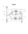
- 6A is an equivalent circuit diagram of the antenna device according to the first embodiment
- FIGS. 6B and 6C are equivalent circuit diagrams of an LC series resonance circuit and an LC parallel resonance circuit applied to the variable resonance circuit, respectively. These are a Smith chart which shows the input impedance of the antenna apparatus by Example 1.
- FIG. 7A to 7D are graphs showing examples of resonance characteristics of the variable resonance circuit.
- FIG. 8 is a perspective view of the antenna device according to the first embodiment.
- FIG. 9 is a plan view of a variable resonance circuit of the antenna device according to the first embodiment.
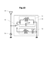
- FIG. 10 is an equivalent circuit diagram of the antenna device according to the second embodiment.
- FIG. 11A and FIG. 11B are a graph and an admittance chart showing the simulation results of the frequency characteristics of the return loss in the state where the variable resonance circuit is not inserted, respectively.
- FIG. 12 is an equivalent circuit diagram of the antenna device according to the second embodiment in a state where the first resonance circuit is shunt-connected.
- 13A and 13B are a graph and an admittance chart showing simulation results of the frequency characteristics of the return loss in the state shown in FIG. 12, respectively.
- FIG. 12 is an equivalent circuit diagram of the antenna device according to the second embodiment in a state where the first resonance circuit is shunt-connected.
- 13A and 13B are a graph and an admittance chart showing simulation results of the frequency characteristics of the return loss in the state shown in FIG
- FIG. 14 is an equivalent circuit diagram of the antenna device according to the second embodiment in a state where the second resonance circuit is shunt-connected.
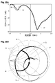
- FIG. 15A and FIG. 15B are a graph and an admittance chart showing simulation results of the frequency characteristics of the return loss in the state shown in FIG.
- FIG. 16A is an equivalent circuit diagram of the antenna device according to the third embodiment
- FIG. 16B is an antenna device equivalent circuit diagram according to a modification of the third embodiment.
- FIG. 17 is an equivalent circuit diagram of the antenna device according to the third embodiment in a state where the first resonance circuit is shunt-connected.
- 18A and 18B are a graph and a admittance chart showing the simulation result of the frequency characteristics of the return loss in the state shown in FIG. 17, respectively.
- FIG. 17 is an equivalent circuit diagram of the antenna device according to the third embodiment in a state where the first resonance circuit is shunt-connected.
- 18A and 18B are a graph and a admittance chart showing the simulation result of the frequency characteristics of the return
- FIG. 19 is an equivalent circuit diagram of the antenna device according to the fourth embodiment.
- FIG. 20 is an equivalent circuit diagram of the antenna device according to the fifth embodiment.
- FIG. 21A is an equivalent circuit diagram of an antenna device according to a reference example, and FIGS. 21B and 21C are a graph and an admittance chart showing simulation results of frequency characteristics of the return loss of the antenna device shown in FIG. 21A, respectively.
- 22A is an equivalent circuit diagram of the antenna device according to the reference example, and FIGS. 22B and 22C are a graph and an admittance chart showing the simulation result of the frequency characteristics of the return loss of the antenna device shown in FIG. 22A, respectively.
- 23A is an equivalent circuit diagram of an antenna device according to a reference example, and FIGS.
- FIGS. 23B and 23C are a graph and an admittance chart showing simulation results of frequency characteristics of return loss of the antenna device shown in FIG. 23A, respectively.
- 24A is an equivalent circuit diagram of the antenna device according to the fifth embodiment in a state where the variable resonance circuit is not shunt-connected
- FIGS. 24B and 24C are graphs of the frequency characteristics of the return loss of the antenna device shown in FIG. 24A, respectively. It is the graph which shows a simulation result, and an admittance chart.
- 25A is an equivalent circuit diagram of the antenna device according to the fifth embodiment in a state where the variable resonance circuit is an inductance.
- FIGS. 25B and 25C are simulation results of the frequency characteristics of the return loss of the antenna device shown in FIG. 25A, respectively.
- FIG. 26A is an equivalent circuit diagram of the antenna device according to the fifth embodiment in a state where the variable resonance circuit is an inductance.
- FIGS. 26B and 26C are simulation results of the frequency characteristics of the return loss of the antenna device shown in FIG. 26A, respectively. It is the graph which shows, and an admittance chart.
- the multiband antenna device in order to evaluate the influence of the switching of the band in the low frequency band on the high frequency band, various antenna devices were manufactured and the antenna characteristics were measured. Hereinafter, the results of this evaluation experiment will be described before describing the examples.
- FIG. 1A shows an equivalent circuit diagram of the antenna device to be evaluated.
- High frequency power is supplied from the power feeding circuit 31 to the radiating element 30.
- a branched monopole antenna was employed as the radiating element 30 as the radiating element 30, a branched monopole antenna was employed. This branched monopole antenna is designed so that matching can be achieved without a matching circuit in a high frequency band.
- FIG. 1B shows the measurement result of the frequency characteristics of the return loss of the radiating element 30.
- the horizontal axis represents frequency in the unit “MHz”, and the vertical axis represents return loss.
- One scale on the vertical axis corresponds to 5 dB.
- the numbers with circles shown in FIG. 1B indicate the lower limit frequency and the upper limit frequency of the operating frequency band.
- Point 1 and point 2 indicate the frequencies 704 MHz and 784 MHz, respectively, and correspond to the lower limit frequency and the upper limit frequency of the band including the band 17 and the band 13.
- Points 3 and 4 indicate 824 MHz and 960 MHz, respectively, and correspond to the lower limit frequency and the upper limit frequency of the band including band 5 and band 8.
- Points 5 and 6 indicate frequencies 1710 MHz and 2170 MHz, respectively, and correspond to the lower limit frequency and the upper limit frequency of the band including band 1 and band 3.
- a band from 704 MHz to 784 MHz including the band 17 and the band 13 is referred to as a “first low frequency band”, and a band from 824 MHz to 960 MHz including the band 5 and the band 8 is referred to as a “second frequency band”.
- the band from 1710 MHz to 2170 MHz including band 1 and band 3 is referred to as a “high frequency band”. It can be seen that the return loss is small and matching is achieved in the high frequency band.
- FIG. 1C shows a locus on the admittance chart of the input impedance of the radiating element 30.
- a constant conductance circle 32 and a constant susceptance circle 33 are drawn.
- the upper half region of the admittance chart corresponds to inductive impedance, and the lower half corresponds to capacitive impedance.
- a constant resistance circle 34 of 50 ⁇ is shown.
- the inside of the constant resistance circle 34 corresponds to an input impedance larger than 50 ⁇ , and the outside of the constant resistance circle 34 corresponds to an input impedance smaller than 50 ⁇ .
- the input impedance in the first low frequency band 35 is smaller than 50 ⁇ and is capacitive.
- the input impedance in the second low frequency band 36 is less than 50 ⁇ and is inductive.
- the locus of input impedance in the high frequency band is located near the center of the admittance chart. That is, impedance matching is taken in the high frequency band.
- a shunt inductor 40 is connected between the feeding point 38 of the radiating element 30 and the ground.
- the shunt inductor 40 has an inductance of 6.8 nH.
- FIG. 2B shows the measurement result of the frequency characteristics of the return loss of the radiating element 30 shown in FIG. 2A
- FIG. 2C shows the locus on the admittance chart of the input impedance of the radiating element 30 shown in FIG. 2A.
- the return loss in the high frequency band 37 is larger than that when the shunt inductor 40 is not connected, but is kept at a sufficiently small value. For this reason, even if the shunt inductor 40 is connected, the operation in the high frequency band 37 is possible. This is because the impedance of the shunt inductor 40 becomes sufficiently large in the high frequency band 37.
- a shunt capacitor 41 is connected between the feeding point 38 of the radiating element 30 and the ground.
- the capacitance of the shunt capacitor 41 is 2 pF.
- FIG. 3B shows the measurement result of the frequency characteristics of the return loss of the radiating element 30 shown in FIG. 3A
- FIG. 3C shows the locus on the admittance chart of the input impedance of the radiating element 30 shown in FIG. 3A.
- the impedance of the shunt capacitor 41 approaches zero. That is, the state is almost the same as the state where the feeding point 38 is grounded. For this reason, in the high frequency band 37, the input impedance of the radiation element 30 becomes remarkably small (in the admittance chart, a point indicating the input impedance approaches the outer peripheral line). Since impedance matching in the high frequency band 37 is lost, the return loss increases as shown in FIG. 3B.
- the antenna apparatus shown in FIGS. 2A to 2C was operable in both the first low frequency band 35 and the high frequency band 37.
- the antenna apparatus shown in FIGS. 3A to 3C can operate in the second low frequency band 36 but is difficult to operate in the high frequency band 37.
- the LC series resonance circuit 42 is shunt-connected between the feeding point 38 of the radiating element 30 and the ground.
- the inductance of the LC series resonant circuit 42 is 18 nH, and the capacitance is 3.2 pF.
- the LC series resonance circuit 42 is equivalent to an inductance of 6.8 nH at about 740 MHz which is the center frequency of the first low frequency band 35. That is, at 740 MHz, the antenna device of FIG. 4A is equivalent to the antenna device of FIG. 2A.
- the reactance of the LC series resonance circuit 42 is larger than the reactance at 740 MHz in a frequency band higher than 740 MHz.
- FIG. 4B shows the measurement result of the frequency characteristics of the return loss of the radiating element 30 shown in FIG. 4A
- FIG. 4C shows the locus on the admittance chart of the input impedance of the radiating element 30 shown in FIG. 4A. Since the LC series resonance circuit 42 shunt-connected to the feeding point 38 of the radiating element 30 exhibits inductive impedance at a frequency higher than the first low frequency band 35, the point indicating the input impedance at each frequency is As indicated by the arrow, the susceptance moves along the constant conductance circle 32 in the direction of decreasing. For this reason, the input impedance in the first low frequency band 35 approaches 50 ⁇ (approaches the center of the admittance chart). Thereby, as shown in FIG. 4B, the return loss in the first low frequency band 35 is reduced.
- the impedance of the LC series resonance circuit 42 is larger than the impedance of the shunt inductor 40 shown in FIG. 2A. For this reason, the impedance matching collapse in the high frequency band 37 is lighter than that of the antenna apparatus shown in FIG. 2A. For this reason, a sufficiently small return loss is maintained in the high frequency band 37.
- the shunt inductor 40 FIG. 2A
- the LC series resonance circuit 42 By replacing the shunt inductor 40 (FIG. 2A) with the LC series resonance circuit 42, the deterioration of the antenna characteristics in the high frequency band 37 can be reduced.
- an LC series resonance circuit 43 is shunt-connected between the feeding point 38 of the radiating element 30 and the ground.
- the inductance of the LC series resonance circuit 43 is 18 nH, and the capacitance is 0.8 pF.
- the LC series resonance circuit 43 exhibits a capacitance of 2 pF at about 880 MHz which is the center frequency of the second low frequency band 36. That is, at 880 MHz, the antenna device of FIG. 5A is equivalent to the antenna device of FIG. 3A.
- the impedance of the LC series resonance circuit 43 becomes inductive in a frequency range higher than the resonance frequency 1326 MHz.
- FIG. 5B shows the measurement result of the frequency characteristics of the return loss of the radiating element 30 shown in FIG. 5A
- FIG. 5C shows the locus on the admittance chart of the input impedance of the radiating element 30 shown in FIG. 5A. Since the LC series resonance circuit 43 shunt-connected to the feeding point 38 of the radiating element 30 exhibits capacitive impedance in the second low frequency band 36, the point indicating the input impedance at each frequency is in the constant conductance circle 32. Along the direction along which the susceptance increases. For this reason, the input impedance in the second low frequency band 36 approaches 50 ⁇ (approaches the center of the admittance chart). Thereby, as shown in FIG. 5B, the return loss in the second low frequency band 36 is reduced.
- the impedance of the shunt capacitor 41 of the antenna device of FIG. 3A approaches 0, but the LC series resonance circuit 43 of the antenna device of FIG. 5A exhibits inductive impedance at a frequency equal to or higher than the resonance frequency. As the value increases, the impedance increases. In the high frequency band 37, the LC series resonance circuit 43 exhibits a sufficiently large impedance, so that the matching condition in the high frequency band 37 is not significantly broken. For this reason, the antenna apparatus shown in FIG. 5A can also operate in the high frequency band 37.
- the operating frequency band of the antenna device is switched between the first low frequency band 35 and the second low frequency band 36. In either case of switching to the first low frequency band 35 or the second low frequency band 36, the operation in the high frequency band is possible.
- FIG. 6A shows an equivalent circuit diagram of the antenna device according to the first embodiment.
- the feeding circuit 31 supplies high-frequency power to the feeding point 38 of the radiating element 30.
- This antenna device is designed to operate in a first low frequency band (for example, 704 MHz to 784 MHz), a second low frequency band (824 MHz to 960 MHz), and a high frequency band (1710 MHz to 2170 MHz).
- a variable resonance circuit 50 is inserted (shunted) between the feeding point 38 and the ground.
- the variable resonance circuit 50 can switch the resonance characteristics between at least two first resonance characteristics and second resonance characteristics.
- the variable resonance circuit 50 includes a first resonance circuit 51 that exhibits first resonance characteristics, a second resonance circuit 52 that exhibits second resonance characteristics, and a switch 53.
- the switch 53 for example, a single pole double throw switch (SPDT switch) is used. The switch 53 switches between a state in which the first resonance circuit 51 is inserted and a state in which the second resonance circuit 52 is inserted between the feeding point 38 and the ground.
- SPDT switch single pole double throw switch
- One of the first resonance circuit 51 and the second resonance circuit 52 is configured by the LC series resonance circuit shown in FIG. 6B, and the other is the LC series resonance circuit shown in FIG. 6B or the LC parallel resonance shown in FIG. 6C. It consists of a circuit.
- the input impedance of the radiating element 30 will be described with reference to the Smith chart (impedance chart) shown in FIG. 6D.
- the input impedance of the radiating element 30 is lower than 50 ⁇ in the first low frequency band 35 and is capacitive. That is, the point indicating the input impedance of the radiating element 30 is located outside the 50 ⁇ constant resistance circle 56 and in the lower half of the Smith chart. For example, the point indicating the input impedance of the radiating element 30 in the first low-frequency band 35 is located in the region 57 shown in FIG. 6D.
- the input impedance of the radiating element 30 When the variable resonance circuit 50 is in an open state where it is not inserted between the feeding point 38 and the ground, the input impedance of the radiating element 30 is lower than 50 ⁇ in the second low frequency band 36 and is capacitive. That is, the point indicating the input impedance of the radiating element 30 is located outside the 50 ⁇ constant resistance circle 56 and in the upper half region of the Smith chart. For example, the point indicating the input impedance of the radiating element 30 in the second low frequency band 36 is located in the region 58 shown in FIG. 6D.
- the input impedance of the radiating element 30 is closer to 50 ⁇ than the input impedance in the first low frequency band 35 and the second low frequency band 36.
- the point indicating the input impedance in the high frequency band 37 of the radiating element 30 is located in a region closer to the center 55 of the Smith chart than the regions 57 and 58 illustrated in FIG. 6D.
- the point indicating the input impedance in the high frequency band 37 is located in a region 59 including the center 55.
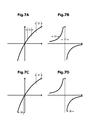
- FIG. 7A and 7B show an example of the resonance characteristics of the first resonance circuit 51 (FIG. 6A).
- the horizontal axis represents frequency, the vertical axis represents reactance, and the origin corresponds to the resonance frequency.
- the resonance characteristics shown in FIG. 7A are realized by an LC series resonance circuit (FIG. 6B), and the resonance characteristics shown in FIG. 7B are realized by an LC parallel resonance circuit (FIG. 6C).
- the first resonant circuit 51 exhibits inductive impedance in the first low frequency band 35 and exhibits higher impedance in the high frequency band 37 than the impedance in the first low frequency band 35.
- the input impedance of the radiating element 30 approaches the center 55 from the region 57 (FIG. 6D). For this reason, impedance matching can be improved in the first low frequency band 35. In the high frequency band 37, since the first resonance circuit 51 exhibits a large impedance, the impedance matching state is maintained.
- the resonance frequency is lower than the first low frequency band 35 as shown in FIG. 7A.
- the impedance in the high frequency band 37 is always higher than the impedance in the first low frequency band 35.
- the resonance frequency is higher than that of the first low frequency band 35 as shown in FIG. 7B.
- the impedance gradually approaches 0 ⁇ as the frequency increases.
- the first frequency is set so that the resonance frequency is located in the vicinity of the high frequency band 37 or inside the high frequency band 37.
- a resonant circuit 51 is designed.
- FIG. 7C shows an example of the resonance characteristics of the second resonance circuit 52.
- the horizontal axis represents frequency, the vertical axis represents reactance, and the origin corresponds to the resonance frequency.
- the resonance characteristics shown in FIG. 7C are realized by an LC series resonance circuit (FIG. 6B).
- the second resonant circuit 52 exhibits capacitive impedance in the second low frequency band 36 and exhibits higher impedance in the high frequency band 37 than in the second low frequency band 36.
- the input impedance of the radiating element 30 approaches the center 55 from the region 58 (FIG. 6D). For this reason, impedance matching can be improved in the second low frequency band 36. In the high frequency band 37, since the second resonance circuit 52 exhibits a large impedance, the impedance matching state is maintained.
- FIG. 7D shows the resonance characteristics of the LC parallel resonance circuit.
- the resonant frequency In order for the LC parallel resonant circuit to be capacitive in the second low frequency band 36, the resonant frequency must be lower than that of the second low frequency band 36. At this time, in the frequency band higher than the second low frequency band 36, the impedance of the LC parallel resonant circuit approaches 0 ⁇ than the impedance in the second low frequency band 36. For this reason, in the high frequency band 37, the condition that the impedance is higher than the impedance in the second low frequency band 36 cannot be satisfied. Therefore, the second resonance circuit 52 cannot be configured with an LC parallel resonance circuit.
- the antenna device when the first resonance circuit 51 is selected by the switch 53, the antenna device is in a state where impedance matching is achieved in the first low frequency band 35 and the high frequency band 37.
- the antenna device When the second resonance circuit 52 is selected by the switch 53, the antenna device is in a state where impedance matching is achieved in the second low frequency band 36 and the high frequency band 37.
- FIG. 8 shows a schematic perspective view of the antenna device according to the first embodiment.
- This antenna device is mounted on, for example, a portable wireless terminal.
- the radiating element 30 is disposed in the vicinity of one edge of the rectangular ground conductor 60.
- a substrate for forming the ground conductor 60 for example, a dielectric substrate such as glass epoxy is used. Conductive films are formed on both surfaces of the dielectric substrate, and the conductive films on both surfaces are connected to each other through a plurality of through holes formed in the dielectric substrate.
- This conductive film constitutes the ground conductor 60.
- ABS resin is used for the dielectric carrier for forming the radiating element 30.
- the radiation element 30 includes a high-frequency radiation element 30A and a low-frequency radiation element 30B.
- the radiating element 30 has a branched monopole antenna structure.
- another antenna that operates in a plurality of bands of a low frequency band and a high frequency band may be used.
- a variable resonance circuit 50 is disposed in the vicinity of the feeding point 38 of the radiating element 30.
- the low-frequency radiating element 30B is preferably extended in a direction away from the ground conductor 60, and the length thereof is preferably 1 ⁇ 4 of the wavelength of the operating frequency.
- the low-frequency radiating element 30 ⁇ / b> B is often disposed along one edge of the ground conductor 60.
- the stray capacitance between the low-frequency radiating element 30B and the ground conductor 60 increases. For this reason, input impedance becomes small in a low frequency band, and it becomes difficult to perform impedance matching without a matching circuit.
- the high-frequency radiating element 30A is shorter than the low-frequency radiating element 30B, it is easy to obtain impedance matching without a matching circuit.
- impedance matching is performed in the first low frequency band or the second low frequency band by shunt connection of the variable resonance circuit 50.
- impedance matching is performed without a matching circuit.
- FIG. 9 shows a plan view of the variable resonance circuit 50.
- the feed point 38 of the radiating element 30 is connected to one of the first resonance circuit 51 and the second resonance circuit 52 by a switch 53 (FIG. 6A).
- the first transmission line 61 connects the first resonance circuit 51 and the ground point 65.
- the second transmission line 62 connects the second resonance circuit 52 and the ground point 65.
- the ground point 65 is connected to a conductive film (ground conductor) on the back surface through a through hole formed in the dielectric substrate.
- the second transmission line 62 connected to the second resonance circuit 52 has a structure equivalent to an open stub.
- the first transmission line 61 connected to the first resonance circuit 51 has a structure equivalent to an open stub.
- these stub-like patterns extend from the ground point 65, the antenna characteristics are not easily affected by unnecessary resonance caused by the stub-like patterns.
- variable resonance circuit 50 is arranged between the vicinity of the feeding point 38 having a relatively low potential compared to the middle of the radiating element 30 in the length direction and the ground. For this reason, it is possible to prevent an excessively high voltage from being applied to the inductor, capacitor, switch, and the like that constitute the variable resonance circuit 50.
- FIG. 10 shows an equivalent circuit diagram of the antenna device according to the second embodiment.
- the first resonance circuit 51 (FIG. 6A) according to the first embodiment is configured by a parallel resonance circuit of a 6.7 nH inductor and a 1.2 pF capacitor
- the second resonance circuit 52 ( FIG. 6A) is composed of a series resonant circuit of an 18 nH inductor and a 0.8 pF capacitor.
- FIG. 11A shows a simulation result of the frequency characteristics of the return loss of the radiating element 30 when the variable resonance circuit 50 is not inserted between the feeding point 38 and the ground.
- the impedance is not matched when the variable resonance circuit 50 (FIG. 10) is not inserted, so that the return loss is large.
- the high frequency band 37 since impedance matching is achieved even when the variable resonance circuit 50 (FIG. 10) is not inserted, the return loss is sufficiently small.
- FIG. 11B shows a locus on the admittance chart of the input impedance of the radiating element 30 in the open state.
- Points 1 and 2 indicate the lower limit value and the upper limit value of the frequency of the first low frequency band 35, respectively.
- Points 3 and 4 indicate the lower limit value and the upper limit value of the frequency of the second low frequency band 36, respectively.
- Points 5 and 6 indicate a lower limit value and an upper limit value of the frequency of the high frequency band 37, respectively.
- the input impedance of the radiating element 30 is greater than 50 ⁇ and is capacitive.
- the input impedance of the radiating element 30 is simply referred to as “input impedance”.
- the input impedance in the second low frequency band 36 is less than 50 ⁇ and is inductive.
- the input impedance in the high frequency band 37 is closer to 50 ⁇ (center of the admittance chart) than the input impedance in the first low frequency band 35 and the second low frequency band 36.
- the point corresponding to the input impedance moves on the admittance chart along the constant conductance circle 32 in a direction in which the susceptance decreases, as indicated by an arrow 71. Thereby, the input impedance in the first low frequency band 35 can be brought close to 50 ⁇ .
- the point corresponding to the input impedance moves on the admittance chart along the constant conductance circle 32 in the direction of increasing the susceptance as indicated by an arrow 72.
- the input impedance in the second low frequency band 36 can be close to 50 ⁇ .
- the simulation result of the return loss when the first resonance circuit 51 is inserted between the feeding point 38 and the ground by the switch 53, and the locus of the input impedance on the admittance chart are shown in FIGS. 13A and 13B, respectively.
- the first resonance circuit 51 exhibits inductive impedance in the first low frequency band 35.
- the point indicating the input impedance in the first low frequency band 35 moves in the direction of the arrow 71. That is, the input impedance approaches 50 ⁇ . Since the impedance matching of the radiating element 30 is improved in the first low frequency band 35, the return loss in the first low frequency band 35 is reduced.
- the impedance of the first resonance circuit 51 is sufficiently high in the high frequency band 37, so that the impedance matching state in the high frequency band is maintained.
- the second resonant circuit 52 exhibits capacitive impedance in the second low frequency band 36.
- the point indicating the input impedance in the second low frequency band 36 moves in the direction of the arrow 72. That is, the input impedance approaches 50 ⁇ . Since the impedance matching of the radiating element 30 is improved in the second low frequency band 36, the return loss in the second low frequency band 36 is reduced.
- the impedance of the second resonance circuit 52 is sufficiently high in the high frequency band 37, so that the impedance matching state in the high frequency band is maintained.
- FIG. 16A shows an equivalent circuit diagram of the antenna device according to the third embodiment.
- the first resonant circuit 51 (FIG. 6A) according to the first embodiment is configured by a series resonant circuit including an 18 nH inductor and a 3.8 pF capacitor.
- the second resonance circuit 52 (FIG. 6A) includes a series resonance circuit of an 18 nH inductor and a 0.8 pF capacitor.
- one of the first resonant circuit 51 and the second resonant circuit 52 is configured by an LC series resonant circuit, and the other is configured by an LC parallel resonant circuit. It consists of a series resonant circuit.
- an 18 nH inductor may be shared by the first resonance circuit 51 and the second resonance circuit 52 to switch between a 0.8 pF capacitor and a 3.8 pF capacitor.
- FIG. 17 the simulation result of the return loss when the first resonance circuit 51 is shunt-connected to the feeding point 38 by the switch 53, and the locus of the input impedance on the admittance chart are shown in FIG. 18A and FIG. 18B, respectively. Shown in The first resonance circuit 51 exhibits inductive impedance in the first low frequency band 35.
- the point indicating the input impedance in the first low frequency band 35 approaches the center of the admittance chart, that is, 50 ⁇ . Since impedance matching is improved in the first low frequency band 35, the return loss is reduced in the first low frequency band 35 as shown in FIG. 18A. Further, in the high frequency band 37, the first resonant circuit 51 exhibits a large impedance, so that the impedance matching condition is hardly affected. For this reason, a state in which impedance matching is achieved in the high frequency band 37 is maintained.
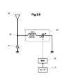
- FIG. 19 shows an equivalent circuit diagram of the antenna device according to the fourth embodiment.
- the variable resonance circuit 50 is configured by a series resonance circuit of a fixed inductor and a variable capacitor. By changing the capacitance of the variable capacitor, the resonance characteristic of the variable resonance circuit can be switched between the first resonance characteristic and the second resonance characteristic.
- the inductance of the fixed inductor is 18 nH, for example.
- the capacitance of the variable capacitor is adjusted to 3.8 pF, the same state as when the first resonance circuit 51 (FIG. 17) of the third embodiment is shunt-connected to the feeding point 38 is realized.
- the capacitance of the variable capacitor is adjusted to 0.8 pF, the same state as that in which the second resonance circuit 52 (FIG. 17) of the third embodiment is shunt-connected to the feeding point 38 is realized.
- the antenna device further includes a sensor 75 and a control circuit 76.
- the sensor 75 detects the approach of an object that affects the radiation characteristics of the radiating element 30, such as a human body or a conductor.
- the detection result by the sensor 75 is given to the control circuit 76.
- the control circuit 76 changes the capacitance of the variable capacitor based on the detection result of the sensor 75. Thereby, it is possible to compensate for the collapse of the impedance matching state due to the approach of the human body or the conductor and maintain the matching state.
- FIG. 20 shows an equivalent circuit diagram of the antenna device according to the fifth embodiment.
- a matching transformer 77 is inserted between the feeding point 38 and the radiating element 30.
- Other configurations are the same as those of the antenna device according to the first embodiment shown in FIG. 6A.
- the antenna device according to the reference example will be described with reference to FIGS. 21A to 23C.
- FIG. 21A shows an equivalent circuit diagram of the antenna device with no matching circuit inserted.
- High frequency power is supplied from the power feeding circuit 31 to the radiating element 30.
- FIGS. 21B and 21C show the simulation results of the frequency characteristics of the return loss of the radiating element 30 shown in FIG. 21A and the locus of the input impedance on the admittance chart. Since no matching circuit is inserted, impedance matching is not achieved in the first low frequency band 35 and the second low frequency band 36. That is, as shown in FIG. 21B, the return loss is large, and as shown in FIG. 21C, the point indicating the input impedance is located in a region far from the center of the admittance chart. Although not shown in FIGS. 21B and 21C, impedance matching is taken in the high frequency band 37 (for example, FIG. 11A).
- FIG. 22A the simulation result of the return loss when the 5.1 nH shunt inductor is inserted and the locus of the input impedance in the admittance chart are shown in FIG. 22B and FIG. 22C, respectively.
- Impedance matching is improved in the first low frequency band 35 by inserting a 5.1 nH shunt inductor.
- the return loss in the vicinity of 787 MHz which is the upper limit value of the frequency of the first low frequency band 35 is larger than the return loss in the vicinity of 704 MHz which is the lower limit value. That is, it cannot be said that a sufficiently low return loss is obtained in the entire first low frequency band 35.
- FIG. 23A the simulation result of the return loss when a 6 pF shunt capacitor is inserted and the locus of the input impedance in the admittance chart are shown in FIG. 23B and FIG. 23C, respectively.
- Impedance matching is improved in the second low frequency band 36 by inserting a 6 pF shunt capacitor.
- the return loss in the vicinity of 824 MHz that is the lower limit value of the frequency of the second low frequency band 36 is larger than the return loss in the vicinity of 960 MHz that is the upper limit value. That is, it cannot be said that a sufficiently low return loss is obtained in the entire second low frequency band 36.
- the vicinity of the upper limit value of the frequency of the first low-frequency band 35 and the second low-frequency band, which are difficult to improve impedance matching with only the shunt inductor and the shunt capacitor, are described. Even in the vicinity of the lower limit of 36 frequencies, the impedance matching can be sufficiently improved.
- the operation and effect of the antenna device according to the fifth embodiment will be described with reference to FIGS. 24A to 26C.
- FIG. 24A the simulation results of the return loss when the variable resonance circuit 50 is not inserted between the feeding point 38 and the ground, and the locus of the input impedance in the admittance chart are shown in FIGS. 24B and 24C, respectively. Show.
- the broken line shown in FIG. 24C indicates the locus of input impedance when the radiating element 30 side is viewed from the feeding point 38 when the variable resonance circuit 50 is not inserted between the feeding point 38 and the ground.
- the inductance connected to the radiating element 30 is 60 nH
- the inductance connected to the feeding point 38 is 120 nH. That is, the transformer ratio is 1: 2. Since the variable resonance circuit 50 is not inserted, impedance matching is not achieved in the first low frequency band 35 and the second low frequency band 36.
- the locus of the input impedance when the radiating element 30 is viewed from the feeding point 38 moves to the right on the admittance chart.
- FIG. 25A the simulation results of the return loss when an 11 nH inductor (shunt inductor) is connected to the position of the variable resonance circuit 50 and the locus of the input impedance on the admittance chart are shown in FIGS. 25B and 25C, respectively. Show. Impedance matching is improved in the first low frequency band 35.
- the point 2 corresponding to the upper limit value of the frequency of the first low frequency band 35 is moved to the right on the admittance chart by connecting the matching transformer, and further, the constant conductance circle 32 is connected by connecting the shunt inductor. Along the direction of decreasing susceptance. Therefore, the input impedance in the vicinity of the upper limit value of the frequency of the first low frequency band 35 can be made sufficiently close to 50 ⁇ .
- FIG. 26A the simulation result of the return loss when a 3.5 pF capacitor (shunt capacitor) is connected to the position of the variable resonance circuit 50, and the locus of the input impedance on the admittance chart are shown in FIG. 26B and FIG. Shown in 26C. Impedance matching is improved in the second low frequency band 36.
- the point 3 corresponding to the lower limit value of the frequency of the second low frequency band 36 moves to the right on the admittance chart by connecting a matching transformer, and further, by connecting a shunt capacitor, a constant conductance circle 32 is obtained.
- the input impedance in the vicinity of the lower limit value of the frequency of the second low frequency band 36 can be made sufficiently close to 50 ⁇ .
Landscapes
- Engineering & Computer Science (AREA)
- Computer Networks & Wireless Communication (AREA)
- Details Of Aerials (AREA)
Abstract
放射素子の給電点と、グランド導体との間に可変共振回路が挿入されている。可変共振回路が挿入されていないとき、放射素子の入力インピーダンスが、第1の低周波数帯において50Ωより低く、かつ容量性であり、第2の低周波数帯において50Ωより低く、かつ誘導性であり、高周波数帯において、50Ωに近い値である。可変共振回路が第1の共振特性を示すとき、可変共振回路は、第1の低周波数帯において誘導性であり、高周波数帯におけるインピーダンスは、第1の低周波数帯におけるインピーダンスよりも高い。可変共振回路が第2の共振特性を示すとき、可変共振回路は、第2の低周波数帯において容量性であり、高周波数帯におけるインピーダンスは、第2の低周波数帯におけるインピーダンスよりも高い。
Description
本発明は、低周波数側の少なくとも2つの周波数帯と、それよりも周波数の高い高周波数帯とで動作するアンテナ装置に関する。
特許文献1に、マルチバンド対応のアンテナ装置が開示されている。このアンテナ装置は、リアクタンス可変部とマッチング部とを有する。リアクタンス可変部は、放射素子に直列接続され、マッチング部は、給電回路とリアクタンス可変部との間にシャント接続されている。リアクタンス可変部及びマッチング部は、ともにインダクタとキャパシタとの並列共振回路で構成される。
リアクタンス可変部の共振周波数を変化させることにより、複数のバンドに対応させることができる。マッチング部によってインピーダンスマッチングが行われる。
リアクタンス可変部の共振周波数を変化させることによって、複数の動作帯域(バンド)から選択された1つのバンドで放射素子を動作させることが可能である。この場合、選択された動作対象のバンド以外のバンドにおいては、放射素子のリターンロスが大きくなり、効率的な動作を行うことが困難である。例えば、低周波数帯の複数のバンドから選択された1つのバンドと、高周波数帯のバンドとの両方で動作させたい場合、低周波数帯のバンドを切り替えるためにリアクタンス可変部の共振周波数を変化させると、その影響が高周波数帯に及んでしまう。これにより、高周波数帯でのインピーダンス整合が崩れてしまう場合がある。
本発明の目的は、低周波数帯のバンドを切り替えても、高周波数帯での動作を継続することが可能なアンテナ装置を提供することである。
本発明の一観点によると、
第1の低周波数帯、前記第1の低周波数帯より高い第2の低周波数帯、及び前記第2の低周波数帯より高い高周波数帯で動作する放射素子と、
グランド導体と、
前記放射素子の給電点と、前記グランド導体との間に挿入され、少なくとも2つの第1の共振特性と第2の共振特性とを切り替えることができる可変共振回路と、
前記可変共振回路が前記給電点と前記グランド導体との間に挿入されていない開放状態のとき、前記放射素子の入力インピーダンスが、前記第1の低周波数帯において50Ωより低く、かつ容量性であり、前記第2の低周波数帯において50Ωより低く、かつ誘導性であり、前記高周波数帯において、前記第1の低周波数帯及び前記第2の低周波数帯における入力インピーダンスよりも50Ωに近く、
前記可変共振回路が前記第1の共振特性を示すとき、前記可変共振回路は、前記第1の低周波数帯において誘導性であり、前記高周波数帯における前記可変共振回路のインピーダンスは、前記第1の低周波数帯における前記可変共振回路のインピーダンスよりも高く、
前記可変共振回路が前記第2の共振特性を示すとき、前記可変共振回路は、前記第2の低周波数帯において容量性であり、前記高周波数帯における前記可変共振回路のインピーダンスは、前記第2の低周波数帯における前記可変共振回路のインピーダンスよりも高いアンテナ装置が提供される。
可変共振回路が第1の共振特性を示すとき、第1の低周波数帯でインピーダンスマッチングが改善する。可変共振回路が第2の共振特性を示すとき、第2の低周波数帯でインピーダンスマッチングが改善する。いずれの状態においても、高周波数帯におけるインピーダンスマッチング状態を維持することができる。
前記第1の低周波数帯において、前記可変共振回路が前記第1の共振特性を示しているときの前記放射素子の入力インピーダンスが、前記開放状態のときの前記放射素子の入力インピーダンスよりも50Ωに近く、
前記第2の低周波数帯において、前記可変共振回路が前記第2の共振特性を示しているときの前記放射素子の入力インピーダンスが、前記開放状態のときの前記放射素子の入力インピーダンスよりも50Ωに近い構成とすることが好ましい。
前記第2の低周波数帯において、前記可変共振回路が前記第2の共振特性を示しているときの前記放射素子の入力インピーダンスが、前記開放状態のときの前記放射素子の入力インピーダンスよりも50Ωに近い構成とすることが好ましい。
これにより、第1の低周波数帯または第2の低周波数帯において、十分なインピーダンスマッチングをとることができる。
前記給電点と前記グランドとが前記開放状態のとき、前記高周波数帯における前記放射素子のリターンロスが、前記第1の低周波数帯及び前記第2の低周波数帯における前記放射素子のリターンロスより小さい構成とすることが好ましい。
すなわち、高周波数帯においては、可変共振回路を挿入しない状態でインピーダンスマッチングがとれていることが好ましい。
一例として、前記第1の低周波数帯は、704MHzから787MHzまでの範囲であり、前記第2の低周波数帯は、824MHzから960MHzまでの範囲であり、前記高周波数帯は、1710MHzから2690MHzまでの範囲である。
前記可変共振回路が、
前記第1の共振特性を示す第1の共振回路と、
前記第2の共振特性を示す第2の共振回路と、
前記放射素子の給電点と前記グランド導体との間に、前記第1の共振回路が挿入された状態と、前記第2の共振回路が挿入された状態とを切り替えるスイッチと
を含む構成とすることが可能である。
前記第1の共振回路及び前記第2の共振回路の一方はLC直列共振回路で構成され、他方は、LC直列共振回路またはLC並列共振回路で構成される。
前記第1の共振特性を示す第1の共振回路と、
前記第2の共振特性を示す第2の共振回路と、
前記放射素子の給電点と前記グランド導体との間に、前記第1の共振回路が挿入された状態と、前記第2の共振回路が挿入された状態とを切り替えるスイッチと
を含む構成とすることが可能である。
前記第1の共振回路及び前記第2の共振回路の一方はLC直列共振回路で構成され、他方は、LC直列共振回路またはLC並列共振回路で構成される。
前記可変共振回路が、相互に直列に接続されたインダクタと可変キャパシタとを含み、前記可変キャパシタのキャパシタンスを変動させることにより、前記第1の共振特性と前記第2の共振特性とが切り換えられる構成とすることも可能である。
さらに、
前記放射素子の放射特性に影響を与える物体の接近を検出するセンサと、
前記センサの検出結果に基づいて、前記可変キャパシタのキャパシタンスを変化させる制御回路と
を有する構成としてもよい。
前記放射素子の放射特性に影響を与える物体の接近を検出するセンサと、
前記センサの検出結果に基づいて、前記可変キャパシタのキャパシタンスを変化させる制御回路と
を有する構成としてもよい。
さらに、前記放射素子と前記給電点との間に挿入されたマッチングトランスを有する構成としてもよい。
可変共振回路が第1の共振特性を示すとき、第1の低周波数帯でインピーダンスマッチングが改善する。可変共振回路が第2の共振特性を示すとき、第2の低周波数帯でインピーダンスマッチングが改善する。いずれの状態においても、高周波数帯におけるインピーダンスマッチング状態を維持することができる。
マルチバンド対応アンテナ装置において、低周波数帯でのバンドの切り換えが高周波数帯に与える影響を評価するために、種々のアンテナ装置を作製し、アンテナ特性を測定した。以下、実施例について説明する前に、この評価実験の結果について説明する。
図1Aに、評価対象のアンテナ装置の等価回路図を示す。給電回路31から放射素子30に高周波電力が供給される。放射素子30として、分岐モノポールアンテナを採用した。この分岐モノポールアンテナは、高周波数帯において整合回路なしでマッチングがとれるように設計されている。
図1Bに、放射素子30のリターンロスの周波数特性の測定結果を示す。横軸は周波数を単位「MHz」で表し、縦軸はリターンロスを表す。縦軸のひと目盛が5dBに相当する。図1Bに示した丸付きの数字は、動作周波数帯域の下限周波数と上限周波数とを示す。点1及び点2が、それぞれ周波数704MHz及び784MHzを示し、バンド17とバンド13とを含む帯域の下限周波数及び上限周波数に相当する。点3及び点4が、それぞれ824MHz及び960MHzを示し、バンド5とバンド8とを含む帯域の下限周波数及び上限周波数に相当する。点5及び点6が、それぞれ周波数1710MHz及び2170MHzを示し、バンド1とバンド3とを含む帯域の下限周波数及び上限周波数に相当する。
本明細書において、バンド17とバンド13とを含む704MHzから784MHzまでの帯域を「第1の低周波数帯」といい、バンド5とバンド8とを含む824MHzから960MHzまでの帯域を「第2の低周波数帯」といい、バンド1とバンド3とを含む1710MHzから2170MHzまでの帯域を「高周波数帯」ということとする。高周波数帯でリターンロスが小さく、マッチングがとれていることがわかる。
図1Cに、放射素子30の入力インピーダンスのアドミタンスチャート上における軌跡を示す。定コンダクタンス円32及び定サセプタンス円33が描かれている。アドミタンスチャートの上半分の領域が誘導性のインピーダンス、下半分が容量性のインピーダンスに対応する。なお、参考のために、50Ωの定抵抗円34を示している。定抵抗円34の内部が、50Ωより大きな入力インピーダンスに対応し、定抵抗円34の外部が、50Ωより小さな入力インピーダンスに対応する。
第1の低周波数帯35における入力インピーダンスは、50Ωより小さく、かつ容量性である。第2の低周波数帯36における入力インピーダンスは、50Ωより小さく、かつ誘導性である。高周波数帯における入力インピーダンスの軌跡は、アドミタンスチャートの中心近傍に位置する。すなわち、高周波数帯においてインピーダンスマッチングがとれている。
図2Aに示したアンテナ装置においては、放射素子30の給電点38とグランドとの間に、シャントインダクタ40が接続されている。一例として、シャントインダクタ40のインダクタンスは6.8nHである。
図2Bに、図2Aに示した放射素子30のリターンロスの周波数特性の測定結果を示し、図2Cに、図2Aに示した放射素子30の入力インピーダンスのアドミタンスチャート上における軌跡を示す。放射素子30の給電点38にシャントインダクタ40を接続すると、各周波数における入力インピーダンスを示す点が、矢印で示すように、定コンダクタンス円32に沿ってサセプタンスが減少する方向移動する。このため、第1の低周波数帯35における入力インピーダンスが50Ωに近づく(アドミタンスチャートの中心に近づく。)。これにより、図2Bに示したように、第1の低周波数帯35におけるリターンロスが低下する。
高周波数帯37におけるリターンロスは、シャントインダクタ40を接続していない場合に比べると大きいが、十分小さな値に保たれている。このため、シャントインダクタ40を接続しても、高周波数帯37における動作が可能である。これは、高周波数帯37においてシャントインダクタ40のインピーダンスが十分大きくなるためである。
図3Aに示したアンテナ装置においては、放射素子30の給電点38とグランドとの間に、シャントキャパシタ41が接続されている。一例として、シャントキャパシタ41のキャパシタンスは2pFである。
図3Bに、図3Aに示した放射素子30のリターンロスの周波数特性の測定結果を示し、図3Cに、図3Aに示した放射素子30の入力インピーダンスのアドミタンスチャート上における軌跡を示す。放射素子30の給電点38にシャントキャパシタ41を接続すると、各周波数における入力インピーダンスを示す点が、矢印で示すように、定コンダクタンス円32に沿ってサセプタンスが増加する方向に移動する。このため、第2の低周波数帯36における入力インピーダンスが50Ωに近づく(アドミタンスチャートの中心に近づく。)。これにより、図3Bに示したように、第2の低周波数帯36におけるリターンロスが低下する。
高周波数帯37において、シャントキャパシタ41のインピーダンスが0に近づく。すなわち、給電点38が接地された状態とほぼ同等の状態になる。このため、高周波数帯37において、放射素子30の入力インピーダンスが著しく小さくなる(アドミタンスチャートにおいて、入力インピーダンスを示す点が外周線に近づく。)。高周波数帯37におけるインピーダンスマッチングが崩れてしまうため、図3Bに示したようにリターンロスが大きくなってしまう。
図2A~図2Cに示したアンテナ装置は、第1の低周波数帯35及び高周波数帯37の両方で動作可能であった。これに対し、図3A~図3Cに示したアンテナ装置は、第2の低周波数帯36で動作可能であるが、高周波数帯37では動作困難である。
図4Aに示したアンテナ装置においては、放射素子30の給電点38とグランドとの間に、LC直列共振回路42がシャント接続されている。一例として、LC直列共振回路42のインダクタンスは18nHであり、キャパシタンスは3.2pFである。このLC直列共振回路42は、第1の低周波数帯35の中心周波数である約740MHzにおいて、6.8nHのインダクタンスと等価である。すなわち、740MHzにおいて、図4Aのアンテナ装置は、図2Aのアンテナ装置と等価である。LC直列共振回路42のリアクタンスは、740MHzより高い周波数帯において、740MHzにおけるリアクタンスより大きくなる。
図4Bに、図4Aに示した放射素子30のリターンロスの周波数特性の測定結果を示し、図4Cに、図4Aに示した放射素子30の入力インピーダンスのアドミタンスチャート上における軌跡を示す。放射素子30の給電点38にシャント接続されたLC直列共振回路42が、第1の低周波数帯35よりも高い周波数において、誘導性のインピーダンスを示すため、各周波数における入力インピーダンスを示す点が、矢印で示すように、定コンダクタンス円32に沿ってサセプタンスが減少する方向に移動する。このため、第1の低周波数帯35における入力インピーダンスが50Ωに近づく(アドミタンスチャートの中心に近づく。)。これにより、図4Bに示したように、第1の低周波数帯35におけるリターンロスが低下する。
高周波数帯37において、LC直列共振回路42のインピーダンスが、図2Aに示したシャントインダクタ40のインピーダンスよりも大きい。このため、高周波数帯37におけるインピーダンスマッチングの崩れが、図2Aに示したアンテナ装置に比べて軽微である。このため、高周波数帯37において、十分小さなリターンロスが維持されている。このように、シャントインダクタ40(図2A)に代えて、LC直列共振回路42を挿入することにより、高周波数帯37におけるアンテナ特性の劣化を軽減することができる。
図5Aに示したアンテナ装置においては、放射素子30の給電点38とグランドとの間に、LC直列共振回路43がシャント接続されている。一例として、LC直列共振回路43のインダクタンスは18nHであり、キャパシタンスは0.8pFである。このLC直列共振回路43は、第2の低周波数帯36の中心周波数である約880MHzにおいて、2pFのキャパシタンスを示す。すなわち、880MHzにおいて、図5Aのアンテナ装置は、図3Aのアンテナ装置と等価である。また、LC直列共振回路43は、その共振周波数1326MHzより高い周波数域においては、LC直列共振回路43のインピーダンスは誘導性になる。
図5Bに、図5Aに示した放射素子30のリターンロスの周波数特性の測定結果を示し、図5Cに、図5Aに示した放射素子30の入力インピーダンスのアドミタンスチャート上における軌跡を示す。放射素子30の給電点38にシャント接続されたLC直列共振回路43が、第2の低周波数帯36において容量性のインピーダンスを示すため、各周波数における入力インピーダンスを示す点が、定コンダクタンス円32に沿ってサセプタンスが増加する方向に移動する。このため、第2の低周波数帯36における入力インピーダンスが50Ωに近づく(アドミタンスチャートの中心に近づく。)。これにより、図5Bに示したように、第2の低周波数帯36におけるリターンロスが低下する。
高周波数帯37において、図3Aのアンテナ装置のシャントキャパシタ41のインピーダンスは0に近づくが、図5Aのアンテナ装置のLC直列共振回路43は、共振周波数以上の周波数で誘導性のインピーダンスを示し、周波数が高くなるにしたがってインピーダンスが高くなる。高周波数帯37において、LC直列共振回路43が十分大きなインピーダンスを示すため、高周波数帯37におけるマッチング条件の崩れが軽微である。このため、図5Aに示したアンテナ装置は、高周波数帯37においても動作可能である。
以下に説明する実施例では、アンテナ装置の動作周波数帯が、第1の低周波数帯35と第2の低周波数帯36とで切り替えられる。第1の低周波数帯35及び第2の低周波数帯36のどちらに切り替えた場合でも、高周波数帯での動作が可能である。
[実施例1]
図6Aに、実施例1によるアンテナ装置の等価回路図を示す。給電回路31が、放射素子30の給電点38に高周波電力を供給する。このアンテナ装置は、第1の低周波数帯(例えば、704MHz~784MHz)、第2の低周波数帯(824MHz~960MHz)、及び高周波数帯(1710MHz~2170MHz)で動作するように設計されている。給電点38とグランドとの間に、可変共振回路50が挿入(シャント接続)されている。
図6Aに、実施例1によるアンテナ装置の等価回路図を示す。給電回路31が、放射素子30の給電点38に高周波電力を供給する。このアンテナ装置は、第1の低周波数帯(例えば、704MHz~784MHz)、第2の低周波数帯(824MHz~960MHz)、及び高周波数帯(1710MHz~2170MHz)で動作するように設計されている。給電点38とグランドとの間に、可変共振回路50が挿入(シャント接続)されている。
可変共振回路50は、共振特性を、少なくとも2つの第1の共振特性と第2の共振特性との間で切り替えることができる。例えば、可変共振回路50は、第1の共振特性を示す第1の共振回路51、第2の共振特性を示す第2の共振回路52、及びスイッチ53を含む。スイッチ53には、例えば単極双投スイッチ(SPDTスイッチ)が用いられる。スイッチ53は、給電点38とグランドとの間に、第1の共振回路51が挿入された状態と、第2の共振回路52が挿入された状態とを切り替える。
第1の共振回路51及び第2の共振回路52の一方は図6Bに示したLC直列共振回路で構成され、他方は、図6Bに示したLC直列共振回路または図6Cに示したLC並列共振回路で構成されている。
図6Dに示したスミスチャート(インピーダンスチャート)を参照して、放射素子30の入力インピーダンスについて説明する。可変共振回路50が給電点38とグランドとの間に挿入されていない開放状態のとき、放射素子30の入力インピーダンスが、第1の低周波数帯35において50Ωより低く、かつ容量性である。すなわち、放射素子30の入力インピーダンスを示す点は、50Ωの定抵抗円56よりも外側で、かつスミスチャートの下半分の領域に位置する。例えば、放射素子30の、第1の低周波数帯35における入力インピーダンスを示す点は、図6Dに示した領域57の中に位置する。
可変共振回路50が給電点38とグランドとの間に挿入されていない開放状態のとき、放射素子30の入力インピーダンスが、第2の低周波数帯36において50Ωより低く、かつ容量性である。すなわち、放射素子30の入力インピーダンスを示す点は、50Ωの定抵抗円56よりも外側で、かつスミスチャートの上半分の領域に位置する。例えば、放射素子30の、第2の低周波数帯36における入力インピーダンスを示す点は、図6Dに示した領域58の中に位置する。
高周波数帯37において、放射素子30の入力インピーダンスは、第1の低周波数帯35及び第2の低周波数帯36における入力インピーダンスよりも50Ωに近い。具体的には、放射素子30の、高周波数帯37における入力インピーダンスを示す点は、図6Dに示した領域57、58よりもスミスチャートの中心55に近い領域に位置する。例えば、高周波数帯37における入力インピーダンスを示す点は、中心55を内包する領域59の中に位置する。
図7A及び図7Bに、第1の共振回路51(図6A)の共振特性の一例を示す。横軸は周波数を表し、縦軸はリアクタンスを表し、原点が共振周波数に対応する。図7Aに示した共振特性は、LC直列共振回路(図6B)で実現され、図7Bに示した共振特性は、LC並列共振回路(図6C)で実現される。第1の共振回路51は、第1の低周波数帯35において、誘導性のインピーダンスを示し、高周波数帯37において、第1の低周波数帯35におけるインピーダンスより高いインピーダンスを示す。
第1の低周波数帯35において誘導性を示す第1の共振回路51が、給電点38にシャント接続されると、放射素子30の入力インピーダンスが領域57(図6D)から中心55に近づく。このため、第1の低周波数帯35においてインピーダンスマッチングを改善することができる。高周波数帯37においては、第1の共振回路51が大きなインピーダンスを示すため、インピーダンスマッチング状態が維持される。
第1の共振回路51がLC直列共振回路で構成される場合には、図7Aに示したように、共振周波数が第1の低周波数帯35よりも低くなる。この場合、高周波数帯37におけるインピーダンスは、常に第1の低周波数帯35におけるインピーダンスより高くなる。
第1の共振回路51がLC並列共振回路で構成される場合には、図7Bに示したように、共振周波数が、第1の低周波数帯35よりも高くなる。周波数が共振周波数より高い領域では、周波数が高くなるにしたがって、インピーダンスが0Ωに漸近する。高周波数帯37におけるインピーダンスを、第1の低周波数帯35におけるインピーダンスより大きくするために、共振周波数が、高周波数帯37の近傍、または高周波数帯37の内側に位置するように、第1の共振回路51が設計される。
図7Cに、第2の共振回路52の共振特性の一例を示す。横軸は周波数を表し、縦軸はリアクタンスを表し、原点が共振周波数に対応する。図7Cに示した共振特性は、LC直列共振回路(図6B)で実現される。第2の共振回路52は、第2の低周波数帯36において容量性のインピーダンスを示し、高周波数帯37において、第2の低周波数帯36におけるインピーダンスより高いインピーダンスを示す。
第2の低周波数帯36において容量性を示す第2の共振回路52が、給電点38にシャント接続されると、放射素子30の入力インピーダンスが領域58(図6D)から中心55に近づく。このため、第2の低周波数帯36においてインピーダンスマッチングを改善することができる。高周波数帯37においては、第2の共振回路52が大きなインピーダンスを示すため、インピーダンスマッチング状態が維持される。
図7Dに、LC並列共振回路の共振特性を示す。LC並列共振回路が第2の低周波数帯36において容量性を示すためには、共振周波数を第2の低周波数帯36よりも低くしなければならない。このとき、第2の低周波数帯36よりも高い周波数帯において、LC並列共振回路のインピーダンスが、第2の低周波数帯36におけるインピーダンスより0Ωに近づく。このため、高周波数帯37において、第2の低周波数帯36におけるインピーダンスより高いインピーダンスを示すという条件を満たすことができない。従って、第2の共振回路52を、LC並列共振回路で構成することができない。
上述のように、スイッチ53により第1の共振回路51が選択されたとき、アンテナ装置は、第1の低周波数帯35及び高周波数帯37において、インピーダンスマッチングがとれた状態になる。スイッチ53により第2の共振回路52が選択されたとき、アンテナ装置は、第2の低周波数帯36及び高周波数帯37において、インピーダンスマッチングがとれた状態になる。
図8に、実施例1によるアンテナ装置の概略斜視図を示す。このアンテナ装置は、例えば携帯無線端末に搭載される。長方形のグランド導体60の1つの縁の近傍に放射素子30が配置される。グランド導体60を形成するための基板として、例えばガラスエポキシ等の誘電体基板が用いられる。誘電体基板の両面に導電膜が形成されており、誘電体基板に形成された複数のスルーホールを介して、両面の導電膜が相互に接続されている。この導電膜がグランド導体60を構成する。放射素子30を形成するための誘電体キャリアには、例えばABS樹脂が用いられる。
放射素子30は、高周波用放射素子30Aと低周波用放射素子30Bとを含む。図8に示された例では、放射素子30が分岐モノポ-ルアンテナ構造を有する。なお、分岐モノポールアンテナに代えて、低周波数帯と高周波数帯との複数バンドで動作する他のアンテナを用いてもよい。例えば、低周波数帯で単共振が生じ、高周波数帯で複共振が生じる無給電素子付きアンテナを用いることも可能である。放射素子30の給電点38の近傍に、可変共振回路50が配置されている。
理想的には、低周波用放射素子30Bを、グランド導体60から遠ざかる方向に引き伸ばし、その長さを動作周波数の波長の1/4にすることが好ましい。ところが、携帯無線端末の小型化等の要請から、低周波用放射素子30Bをグランド導体60から遠ざかる方向に引き延ばすことが困難である。このため、低周波用放射素子30Bは、グランド導体60の一つの縁に沿って配置されることが多い。
低周波用放射素子30Bをグランド導体60の縁に沿わせると、低周波用放射素子30Bとグランド導体60との間の浮遊容量が大きくなる。このため、低周波数帯において入力インピーダンスが小さくなり、整合回路無しでインピーダンスマッチングをとることが困難になる。これに対し、高周波用放射素子30Aは、低周波用放射素子30Bより短いため、整合回路無しでインピーダンスマッチングをとることが容易である。
実施例1においては、可変共振回路50をシャント接続することにより、第1の低周波数帯または第2の低周波数帯においてインピーダンスマッチングがとられる。高周波数帯においては、整合回路無しでインピーダンスマッチングがとられている。特に、グランド導体60から、低周波用放射素子30Bの最遠端までの距離が、動作周波数の波長に比べて短いほど、実施例1による構成を採用することの顕著な効果が得られる。
図9に、可変共振回路50の平面図を示す。放射素子30の給電点38が、スイッチ53(図6A)により、第1の共振回路51及び第2の共振回路52の一方に接続される。第1の伝送線路61が、第1の共振回路51と接地点65とを接続する。第2の伝送線路62が、第2の共振回路52と接地点65とを接続する。接地点65は、誘電体基板に形成されたスルーホールを介して、背面の導電膜(グランド導体)に接続されている。
第1の共振回路51が給電点38に接続されているとき、第2の共振回路52に接続されている第2の伝送線路62がオープンスタブと同等の構造を有する。同様に、第2の共振回路52が給電点38に接続されているとき、第1の共振回路51に接続されている第1の伝送線路61がオープンスタブと同等の構造を有する。ところが、これらのスタブ状のパターンは、接地点65から伸びているため、アンテナ特性が、スタブ状パターンに起因する不要共振等による影響を受けにくい。
可変共振回路50が、放射素子30の長さ方向の途中に比べて比較的電位の低い給電点38の近傍と、グランドとの間に配置される。このため、可変共振回路50を構成するインダクタ、キャパシタ、スイッチ等に、過度に高い電圧が印加されることを防止できる。
[実施例2]
図10に、実施例2によるアンテナ装置の等価回路図を示す。実施例2においては、実施例1による第1の共振回路51(図6A)が、6.7nHのインダクタと、1.2pFのキャパシタとの並列共振回路で構成され、第2の共振回路52(図6A)が、18nHのインダクタと0.8pFのキャパシタとの直列共振回路で構成される。
図10に、実施例2によるアンテナ装置の等価回路図を示す。実施例2においては、実施例1による第1の共振回路51(図6A)が、6.7nHのインダクタと、1.2pFのキャパシタとの並列共振回路で構成され、第2の共振回路52(図6A)が、18nHのインダクタと0.8pFのキャパシタとの直列共振回路で構成される。
図11Aに、給電点38とグランドとの間に、可変共振回路50が挿入されていない開放状態のときにおける放射素子30のリターンロスの周波数特性のシミュレーション結果を示す。第1の低周波数帯35及び第2の低周波数帯36においては、可変共振回路50(図10)が挿入されていない状態でインピーダンスマッチングがとれていないため、リターンロスが大きい。高周波数帯37においては、可変共振回路50(図10)が挿入されていない状態でもインピーダンスマッチングがとれているため、リターンロスが十分小さい。
図11Bに、開放状態のときの放射素子30の入力インピーダンスのアドミタンスチャート上における軌跡を示す。点1と点2が、それぞれ第1の低周波数帯35の周波数の下限値及び上限値を示す。点3と点4が、それぞれ第2の低周波数帯36の周波数の下限値及び上限値を示す。点5と点6が、それぞれ高周波数帯37の周波数の下限値及び上限値を示す。第1の低周波数帯35において、放射素子30の入力インピーダンスは50Ωより大きく、かつ容量性である。以下、放射素子30の入力インピーダンスを、単に「入力インピーダンス」という。第2の低周波数帯36における入力インピーダンスは50Ωより小さく、かつ誘導性である。高周波数帯37における入力インピーダンスは、第1の低周波数帯35及び第2の低周波数帯36における入力インピーダンスよりも50Ω(アドミタンスチャートの中心)に近い。
給電点38(図10)にシャントインダクタンスを挿入すると、アドミタンスチャート上において、入力インピーダンスに対応する点が矢印71で示すように、定コンダクタンス円32に沿ってサセプタンスが減少する方向に移動する。これにより、第1の低周波数帯35における入力インピーダンスを50Ωに近づけることができる。
給電点38(図10)にシャントキャパシタンスを挿入すると、アドミタンスチャート上において、入力インピーダンスに対応する点が矢印72で示すように、定コンダクタンス円32に沿ってサセプタンスが増加する方向に移動する。これにより、第2の低周波数帯36における入力インピーダンスを50Ωに近づけることができる。
図12に示すように、スイッチ53によって第1の共振回路51が給電点38とグランドとの間に挿入された状態のときのリターンロスのシミュレーション結果、及びアドミタンスチャート上における入力インピーダンスの軌跡を、それぞれ図13A及び図13Bに示す。第1の共振回路51は、第1の低周波数帯35において誘導性のインピーダンスを示す。このため、図13Bに示すように、第1の低周波数帯35における入力インピーダンスを示す点が、矢印71の方向に移動する。すなわち、入力インピーダンスが50Ωに近づく。第1の低周波数帯35において放射素子30のインピーダンスマッチングが改善するため、第1の低周波数帯35におけるリターンロスが小さくなる。
第1の共振回路51がシャント接続されても、第1の共振回路51のインピーダンスが高周波数帯37において十分高いため、高周波数帯におけるインピーダンスマッチングがとれた状態が維持される。
図14に示すように、スイッチ53によって第2の共振回路52が給電点38とグランドとの間に挿入された状態のときのリターンロスのシミュレーション結果、及びアドミタンスチャート上における入力インピーダンスの軌跡を、それぞれ図15A及び図15Bに示す。第2の共振回路52は、第2の低周波数帯36において容量性のインピーダンスを示す。このため、図15Bに示すように、第2の低周波数帯36における入力インピーダンスを示す点が、矢印72の方向に移動する。すなわち、入力インピーダンスが50Ωに近づく。第2の低周波数帯36において放射素子30のインピーダンスマッチングが改善するため、第2の低周波数帯36におけるリターンロスが小さくなる。
第2の共振回路52がシャント接続されても、第2の共振回路52のインピーダンスが高周波数帯37において十分高いため、高周波数帯におけるインピーダンスマッチングがとれた状態が維持される。
[実施例3]
図16Aに、実施例3によるアンテナ装置の等価回路図を示す。実施例3においては、実施例1による第1の共振回路51(図6A)が、18nHのインダクタと、3.8pFのキャパシタとの直列共振回路で構成される。第2の共振回路52(図6A)は、実施例2の第2の共振回路52(図10)と同様に、18nHのインダクタと0.8pFのキャパシタとの直列共振回路で構成される。実施例2では、第1の共振回路51及び第2の共振回路52の一方がLC直列共振回路で構成され、他方がLC並列共振回路で構成されていたが、実施例3では、両者がLC直列共振回路で構成されている。
図16Aに、実施例3によるアンテナ装置の等価回路図を示す。実施例3においては、実施例1による第1の共振回路51(図6A)が、18nHのインダクタと、3.8pFのキャパシタとの直列共振回路で構成される。第2の共振回路52(図6A)は、実施例2の第2の共振回路52(図10)と同様に、18nHのインダクタと0.8pFのキャパシタとの直列共振回路で構成される。実施例2では、第1の共振回路51及び第2の共振回路52の一方がLC直列共振回路で構成され、他方がLC並列共振回路で構成されていたが、実施例3では、両者がLC直列共振回路で構成されている。
図16Bに示すように、18nHのインダクタを第1の共振回路51と第2の共振回路52とで共用し、0.8pFのキャパシタと3.8pFのキャパシタとを切り替える構成としてもよい。
図17に示すように、スイッチ53によって第1の共振回路51が給電点38にシャント接続されたときのリターンロスのシミュレーション結果、及びアドミタンスチャート上における入力インピーダンスの軌跡を、それぞれ図18A及び図18Bに示す。第1の共振回路51は、第1の低周波数帯35において誘導性のインピーダンスを示す。
図18Bに示すように、第1の低周波数帯35における入力インピーダンスを示す点が、アドミタンスチャートの中心、すなわち50Ωに近づく。第1の低周波数帯35においてインピーダンスマッチングが改善するため、図18Aに示したように、第1の低周波数帯35においてリターンロスが低下している。また、高周波数帯37においては、第1の共振回路51が大きなインピーダンスを示すため、インピーダンスマッチング条件にほとんど影響を与えない。このため、高周波数帯37においてインピーダンスマッチングがとれた状態が維持される。
スイッチ53によって第2の共振回路52(図17)が給電点38にシャント接続された状態は、実施例の図14に示した状態と同一である。このため、図15A及び図15Bに示したように、第2の低周波数帯36において、インピーダンスマッチングが改善され、リターンロスが低下する。
[実施例4]
図19に、実施例4によるアンテナ装置の等価回路図を示す。実施例4においては、可変共振回路50が、固定インダクタと可変キャパシタとの直列共振回路で構成される。可変キャパシタのキャパシタンスを変動させることにより、可変共振回路の共振特性を、第1の共振特性と第2の共振特性との間で切り換えることができる。
図19に、実施例4によるアンテナ装置の等価回路図を示す。実施例4においては、可変共振回路50が、固定インダクタと可変キャパシタとの直列共振回路で構成される。可変キャパシタのキャパシタンスを変動させることにより、可変共振回路の共振特性を、第1の共振特性と第2の共振特性との間で切り換えることができる。
固定インダクタのインダクタンスは、例えば18nHである。可変キャパシタのキャパシタンスを3.8pFに調整すると、実施例3の第1の共振回路51(図17)が給電点38にシャント接続された状態と同一の状態が実現される。可変キャパシタのキャパシタンスを0.8pFに調整すると、実施例3の第2の共振回路52(図17)が給電点38にシャント接続された状態と同一の状態が実現される。
実施例4によるアンテナ装置は、さらにセンサ75及び制御回路76を含む。センサ75は、放射素子30の放射特性に影響を与える物体、例えば人体、導電体等の接近を検出する。センサ75による検出結果が制御回路76に与えられる。制御回路76は、センサ75の検出結果に基づいて、可変キャパシタのキャパシタンスを変化させる。これにより、人体や導電体の接近によるインピーダンスマッチング状態の崩れを補償し、マッチング状態を維持することが可能になる。
[実施例5]
図20に、実施例5によるアンテナ装置の等価回路図を示す。実施例5によるアンテナ装置は、給電点38と放射素子30との間にマッチングトランス77が挿入されている。その他の構成は、図6Aに示した実施例1によるアンテナ装置の構成と同一である。実施例5によるアンテナ装置の動作及び効果を説明する前に、図21A~図23Cを参照して、参考例によるアンテナ装置について説明する。
図20に、実施例5によるアンテナ装置の等価回路図を示す。実施例5によるアンテナ装置は、給電点38と放射素子30との間にマッチングトランス77が挿入されている。その他の構成は、図6Aに示した実施例1によるアンテナ装置の構成と同一である。実施例5によるアンテナ装置の動作及び効果を説明する前に、図21A~図23Cを参照して、参考例によるアンテナ装置について説明する。
図21Aに、整合回路が挿入されていない状態のアンテナ装置の等価回路図を示す。給電回路31から放射素子30に高周波電力が供給される。図21B及び図21Cに、それぞれ図21Aに示した放射素子30のリターンロスの周波数特性のシミュレーション結果、及びアドミタンスチャート上における入力インピーダンスの軌跡を示す。整合回路が挿入されていないため、第1の低周波数帯35及び第2の低周波数帯36においてインピーダンス整合がとれていない。すなわち、図21Bに示したように、リターンロスが大きく、図21Cに示したように、入力インピーダンスを示す点がアドミタンスチャートの中心から遠い領域に位置する。図21B及び図21Cでは表されていないが、高周波数帯37(例えば図11A)においては、インピーダンスマッチングがとれている。
図22Aに示すように、5.1nHのシャントインダクタを挿入したときのリターンロスのシミュレーション結果、及びアドミタンスチャートにおける入力インピーダンスの軌跡を、それぞれ図22B及び図22Cに示す。5.1nHのシャントインダクタを挿入することにより、第1の低周波数帯35においてインピーダンスマッチングが改善される。ところが、第1の低周波数帯35の周波数の上限値である787MHzの近傍におけるリターンロスが、下限値である704MHzの近傍におけるリターンロスに比べて大きいことがわかる。すなわち、第1の低周波数帯35の全域において、十分低いリターンロスが得られているとはいえない。
図22Cに示すように、シャントインダクタを挿入すると、周波数の上限値に対応する点2が、定コンダクタンス円32に沿ってサセプタンスが減少する方向に移動する。図22Cに示した条件では、点2を定コンダクタンス円32に沿ってサセプタンスが減少する方向に移動させたとしても、アドミタンスチャートの中心55に十分近づけることができない。すなわち、第1の低周波数帯35の周波数の上限値近傍において、シャントインダクタのみでは、インピーダンスマッチングを改善することが困難である。
図23Aに示すように、6pFのシャントキャパシタを挿入したときのリターンロスのシミュレーション結果、及びアドミタンスチャートにおける入力インピーダンスの軌跡を、それぞれ図23B及び図23Cに示す。6pFのシャントキャパシタを挿入することにより、第2の低周波数帯36においてインピーダンスマッチングが改善される。ところが、第2の低周波数帯36の周波数の下限値である824MHzの近傍におけるリターンロスが、上限値である960MHzの近傍におけるリターンロスに比べて大きい。すなわち、第2の低周波数帯36の全域において、十分低いリターンロスが得られているとはいえない。
図23Cに示すように、シャントキャパシタを挿入すると、周波数の下限値に対応する点3が、定コンダクタンス円32に沿ってサセプタンスが増加する方向に移動する。図23Cに示した条件では、点3を定コンダクタンス円32に沿ってサセプタンスが増加する方向に移動させたとしても、アドミタンスチャートの中心55に十分近づけることができない。すなわち、第2の低周波数帯36の周波数の下限値近傍において、シャントインダクタのみでは、インピーダンスマッチングを改善することが困難である。
以下に説明する実施例5によるアンテナ装置においては、シャントインダクタやシャントキャパシタのみではインピーダンスマッチングの改善が困難であった第1の低周波数帯35の周波数の上限値近傍、及び第2の低周波数帯36の周波数の下限値近傍においても、インピーダンスマッチングの十分な改善が可能である。図24A~図26Cを参照して、実施例5によるアンテナ装置の動作及び効果について説明する。
図24Aに示すように、給電点38とグランドとの間に可変共振回路50が挿入されていないときのリターンロスのシミュレーション結果、及びアドミタンスチャートにおける入力インピーダンスの軌跡を、それぞれ図24B及び図24Cに示す。図24Cに示した破線は、給電点38とグランドとの間に可変共振回路50が挿入されていない状態のときの、給電点38から放射素子30側を見た入力インピーダンスの軌跡を示している。マッチングトランス77の2つのインダクタンスのうち、放射素子30に接続されたインダクタンスが60nHであり、給電点38に接続されたインダクタンスが120nHである。すなわち、トランス比が1:2である。可変共振回路50が挿入されていないため、第1の低周波数帯35及び第2の低周波数帯36においてインピーダンスマッチングがとれていない。
図24Cに示すように、マッチングトランスを挿入することによって、給電点38から放射素子30を見た入力インピーダンスの軌跡が、アドミタンスチャート上で右方に移動する。
図25Aに示すように、可変共振回路50の位置に11nHのインダクタ(シャントインダクタ)を接続したときのリターンロスのシミュレーション結果、及びアドミタンスチャート上における入力インピーダンスの軌跡を、それぞれ図25B及び図25Cに示す。第1の低周波数帯35においてインピーダンスマッチングが改善されている。
第1の低周波数帯35の周波数の上限値に相当する点2が、マッチングトランスを接続することによってアドミタンスチャート上において右方に移動し、さらに、シャントインダクタを接続することによって、定コンダクタンス円32に沿ってサセプタンスが減少する方向に移動する。このため、第1の低周波数帯35の周波数の上限値の近傍における入力インピーダンスを50Ωに十分近づけることが可能になる。
マッチングトランスを接続していないアンテナ装置のリターンロス(図22B)と、マッチングトランスを接続しているアンテナ装置のリターンロス(図25B)とを比較すると、第1の低周波数帯35の全域において、バランスよく、低いリターンロスが得られていることがわかる。
図26Aに示すように、可変共振回路50の位置に3.5pFのキャパシタ(シャントキャパシタ)を接続したときのリターンロスのシミュレーション結果、及びアドミタンスチャート上における入力インピーダンスの軌跡を、それぞれ図26B及び図26Cに示す。第2の低周波数帯36においてインピーダンスマッチングが改善されている。
第2の低周波数帯36の周波数の下限値に相当する点3が、マッチングトランスを接続することによってアドミタンスチャート上において右方に移動し、さらに、シャントキャパシタを接続することによって、定コンダクタンス円32に沿ってサセプタンスが増加する方向に移動する。このため、第2の低周波数帯36の周波数の下限値の近傍における入力インピーダンスを50Ωに十分近づけることが可能になる。
マッチングトランスを接続していないアンテナ装置のリターンロス(図23B)と、マッチングトランスを接続しているアンテナ装置のリターンロス(図26B)とを比較すると、第2の低周波数帯36の全域において、バランスよく、低いリターンロスが得られていることがわかる。
以上実施例に沿って本発明を説明したが、本発明はこれらに制限されるものではない。例えば、種々の変更、改良、組み合わせ等が可能なことは当業者に自明であろう。
30 放射素子
30A 高周波用放射素子
30B 低周波用放射素子
31 給電回路
32 定コンダクタンス円
33 定サセプタンス円
34 定抵抗円
35 第1の低周波数帯
36 第2の低周波数帯
37 高周波数帯
38 給電点
40 シャントインダクタンス
41 シャントキャパシタンス
42、43 LC直列共振回路
50 可変共振回路
51 第1の共振回路
52 第2の共振回路
53 スイッチ
55 スミスチャートの中心
56 50Ωの定抵抗円
57 第1の低周波数帯における入力インピーダンス領域
58 第2の低周波数帯における入力インピーダンス領域
59 高周波数帯における入力インピーダンス領域
60 グランド導体
61、62 伝送線路
65 接地点
71、72 矢印
75 センサ
76 制御回路
77 マッチングトランス
Claims (8)
- 第1の低周波数帯、前記第1の低周波数帯より高い第2の低周波数帯、及び前記第2の低周波数帯より高い高周波数帯で動作する放射素子と、
グランド導体と、
前記放射素子の給電点と、前記グランド導体との間に挿入され、少なくとも2つの第1の共振特性と第2の共振特性とを切り替えることができる可変共振回路と、
前記可変共振回路が前記給電点と前記グランド導体との間に挿入されていない開放状態のとき、前記放射素子の入力インピーダンスが、前記第1の低周波数帯において50Ωより低く、かつ容量性であり、前記第2の低周波数帯において50Ωより低く、かつ誘導性であり、前記高周波数帯において、前記第1の低周波数帯及び前記第2の低周波数帯における入力インピーダンスよりも50Ωに近く、
前記可変共振回路が前記第1の共振特性を示すとき、前記可変共振回路は、前記第1の低周波数帯において誘導性であり、前記高周波数帯における前記可変共振回路のインピーダンスは、前記第1の低周波数帯における前記可変共振回路のインピーダンスよりも高く、
前記可変共振回路が前記第2の共振特性を示すとき、前記可変共振回路は、前記第2の低周波数帯において容量性であり、前記高周波数帯における前記可変共振回路のインピーダンスは、前記第2の低周波数帯における前記可変共振回路のインピーダンスよりも高いアンテナ装置。 - 前記第1の低周波数帯において、前記可変共振回路が前記第1の共振特性を示しているときの前記放射素子の入力インピーダンスが、前記開放状態のときの前記放射素子の入力インピーダンスよりも50Ωに近く、
前記第2の低周波数帯において、前記可変共振回路が前記第2の共振特性を示しているときの前記放射素子の入力インピーダンスが、前記開放状態のときの前記放射素子の入力インピーダンスよりも50Ωに近い請求項1に記載のアンテナ装置。 - 前記給電点と前記グランド導体とが前記開放状態のとき、前記高周波数帯における前記放射素子のリターンロスが、前記第1の低周波数帯及び前記第2の低周波数帯における前記放射素子のリターンロスより小さい請求項1または2に記載のアンテナ装置。
- 前記第1の低周波数帯は、704MHzから787MHzまでの範囲であり、前記第2の低周波数帯は、824MHzから960MHzまでの範囲であり、前記高周波数帯は、1710MHzから2690MHzまでの範囲である請求項1乃至3のいずれか1項に記載のアンテナ装置。
- 前記可変共振回路は、
前記第1の共振特性を示す第1の共振回路と、
前記第2の共振特性を示す第2の共振回路と、
前記放射素子の前記給電点と前記グランド導体との間に、前記第1の共振回路が挿入された状態と、前記第2の共振回路が挿入された状態とを切り替えるスイッチと
を含み、
前記第1の共振回路及び前記第2の共振回路の一方はLC直列共振回路で構成され、他方は、LC直列共振回路またはLC並列共振回路で構成されている請求項1乃至4のいずれか1項に記載のアンテナ装置。 - 前記可変共振回路は、相互に直列に接続されたインダクタと可変キャパシタとを含み、前記可変キャパシタのキャパシタンスを変動させることにより、前記第1の共振特性と前記第2の共振特性とが切り換えられる請求項1乃至4のいずれか1項に記載のアンテナ装置。
- さらに、
前記放射素子の放射特性に影響を与える物体の接近を検出するセンサと、
前記センサの検出結果に基づいて、前記可変キャパシタのキャパシタンスを変化させる制御回路と
を有する請求項6に記載のアンテナ装置。 - さらに、前記放射素子と前記給電点との間に挿入されたマッチングトランスを有する請求項1乃至7のいずれか1項に記載のアンテナ装置。
Priority Applications (1)
| Application Number | Priority Date | Filing Date | Title |
|---|---|---|---|
| US14/887,411 US9634390B2 (en) | 2013-05-10 | 2015-10-20 | Antenna device |
Applications Claiming Priority (2)
| Application Number | Priority Date | Filing Date | Title |
|---|---|---|---|
| JP2013-100156 | 2013-05-10 | ||
| JP2013100156 | 2013-05-10 |
Related Child Applications (1)
| Application Number | Title | Priority Date | Filing Date |
|---|---|---|---|
| US14/887,411 Continuation US9634390B2 (en) | 2013-05-10 | 2015-10-20 | Antenna device |
Publications (1)
| Publication Number | Publication Date |
|---|---|
| WO2014181569A1 true WO2014181569A1 (ja) | 2014-11-13 |
Family
ID=51867055
Family Applications (1)
| Application Number | Title | Priority Date | Filing Date |
|---|---|---|---|
| PCT/JP2014/055350 WO2014181569A1 (ja) | 2013-05-10 | 2014-03-04 | アンテナ装置 |
Country Status (2)
| Country | Link |
|---|---|
| US (1) | US9634390B2 (ja) |
| WO (1) | WO2014181569A1 (ja) |
Cited By (3)
| Publication number | Priority date | Publication date | Assignee | Title |
|---|---|---|---|---|
| CN109638455A (zh) * | 2018-12-12 | 2019-04-16 | 维沃移动通信有限公司 | 天线结构及通信终端 |
| US10424841B2 (en) | 2015-07-31 | 2019-09-24 | Murata Manufacturing Co., Ltd. | Antenna matching circuit, antenna circuit, front-end circuit, and communication apparatus |
| WO2021090487A1 (ja) * | 2019-11-08 | 2021-05-14 | ソニー株式会社 | 整合回路およびアンテナ装置 |
Families Citing this family (14)
| Publication number | Priority date | Publication date | Assignee | Title |
|---|---|---|---|---|
| JP6212405B2 (ja) * | 2014-02-19 | 2017-10-11 | シャープ株式会社 | 無線機 |
| US10290940B2 (en) * | 2014-03-19 | 2019-05-14 | Futurewei Technologies, Inc. | Broadband switchable antenna |
| WO2016019582A1 (zh) * | 2014-08-08 | 2016-02-11 | 华为技术有限公司 | 天线装置和终端 |
| US10381717B2 (en) * | 2017-03-17 | 2019-08-13 | Nxp B.V. | Automotive antenna |
| US11290084B2 (en) | 2017-05-24 | 2022-03-29 | Anlotek Limited | Apparatus and method for controlling a resonator |
| CN107967026B (zh) * | 2017-11-23 | 2019-10-25 | Oppo广东移动通信有限公司 | 天线组件、终端设备及改善天线辐射性能的方法 |
| WO2020050341A1 (ja) * | 2018-09-07 | 2020-03-12 | 株式会社村田製作所 | アンテナ素子、アンテナモジュールおよび通信装置 |
| US11277110B2 (en) | 2019-09-03 | 2022-03-15 | Anlotek Limited | Fast frequency switching in a resonant high-Q analog filter |
| CN115427911A (zh) | 2019-12-05 | 2022-12-02 | 安乐泰克有限公司 | 在频率合成中使用稳定的可调谐有源反馈模拟滤波器 |
| EP3926828A1 (en) | 2020-06-15 | 2021-12-22 | Anlotek Limited | Tunable bandpass filter with high stability and orthogonal tuning |
| CN112397902B (zh) * | 2020-10-23 | 2023-06-20 | Oppo广东移动通信有限公司 | 一种天线及其阻抗匹配方法、终端 |
| CN114447574A (zh) * | 2020-11-04 | 2022-05-06 | 富泰京精密电子(烟台)有限公司 | 天线结构及具有该天线结构的无线通信装置 |
| US11955942B2 (en) | 2021-02-27 | 2024-04-09 | Anlotek Limited | Active multi-pole filter |
| TWI793867B (zh) * | 2021-11-19 | 2023-02-21 | 啓碁科技股份有限公司 | 通訊裝置 |
Citations (4)
| Publication number | Priority date | Publication date | Assignee | Title |
|---|---|---|---|---|
| JPS63177622A (ja) * | 1986-11-14 | 1988-07-21 | Seiko Epson Corp | アンテナ回路 |
| JP2002076750A (ja) * | 2000-08-24 | 2002-03-15 | Murata Mfg Co Ltd | アンテナ装置およびそれを備えた無線機 |
| WO2011024280A1 (ja) * | 2009-08-27 | 2011-03-03 | 株式会社 東芝 | アンテナ装置及び通信装置 |
| JP2011155626A (ja) * | 2009-12-28 | 2011-08-11 | Fujitsu Ltd | アンテナ装置及び通信装置 |
Family Cites Families (11)
| Publication number | Priority date | Publication date | Assignee | Title |
|---|---|---|---|---|
| EP1280233A4 (en) * | 2000-04-13 | 2004-12-22 | Mitsubishi Electric Corp | ANTENNA ELEMENT AND PORTABLE COMMUNICATION TERMINAL |
| JP2003249811A (ja) * | 2001-12-20 | 2003-09-05 | Murata Mfg Co Ltd | 複共振アンテナ装置 |
| JP4132016B2 (ja) | 2001-12-25 | 2008-08-13 | 松下電器産業株式会社 | 整合回路およびプラズマ処理装置 |
| JP2005311762A (ja) * | 2004-04-22 | 2005-11-04 | Matsushita Electric Ind Co Ltd | 可変整合回路 |
| JP4959956B2 (ja) | 2005-06-07 | 2012-06-27 | 株式会社日立製作所 | アンテナ |
| EP2104178A4 (en) * | 2007-01-19 | 2014-05-28 | Murata Manufacturing Co | ANTENNA MODULE AND WIRELESS COMMUNICATION DEVICE |
| JP2009278192A (ja) * | 2008-05-12 | 2009-11-26 | Sony Ericsson Mobilecommunications Japan Inc | アンテナ装置及び通信端末装置 |
| JP5304890B2 (ja) * | 2009-04-01 | 2013-10-02 | 株式会社村田製作所 | アンテナ整合回路、アンテナ装置及びアンテナ装置の設計方法 |
| CN104953242B (zh) * | 2010-01-19 | 2019-03-26 | 株式会社村田制作所 | 天线装置及通信终端设备 |
| JP4761009B1 (ja) * | 2010-08-11 | 2011-08-31 | 株式会社村田製作所 | 周波数安定化回路、アンテナ装置及び通信端末機器 |
| CN103141031B (zh) * | 2011-02-23 | 2015-05-20 | 株式会社村田制作所 | 阻抗变换电路以及通信终端装置 |
-
2014
- 2014-03-04 WO PCT/JP2014/055350 patent/WO2014181569A1/ja active Application Filing
-
2015
- 2015-10-20 US US14/887,411 patent/US9634390B2/en active Active
Patent Citations (4)
| Publication number | Priority date | Publication date | Assignee | Title |
|---|---|---|---|---|
| JPS63177622A (ja) * | 1986-11-14 | 1988-07-21 | Seiko Epson Corp | アンテナ回路 |
| JP2002076750A (ja) * | 2000-08-24 | 2002-03-15 | Murata Mfg Co Ltd | アンテナ装置およびそれを備えた無線機 |
| WO2011024280A1 (ja) * | 2009-08-27 | 2011-03-03 | 株式会社 東芝 | アンテナ装置及び通信装置 |
| JP2011155626A (ja) * | 2009-12-28 | 2011-08-11 | Fujitsu Ltd | アンテナ装置及び通信装置 |
Cited By (5)
| Publication number | Priority date | Publication date | Assignee | Title |
|---|---|---|---|---|
| US10424841B2 (en) | 2015-07-31 | 2019-09-24 | Murata Manufacturing Co., Ltd. | Antenna matching circuit, antenna circuit, front-end circuit, and communication apparatus |
| CN109638455A (zh) * | 2018-12-12 | 2019-04-16 | 维沃移动通信有限公司 | 天线结构及通信终端 |
| WO2020119349A1 (zh) * | 2018-12-12 | 2020-06-18 | 维沃移动通信有限公司 | 天线结构及通信终端 |
| US11967780B2 (en) | 2018-12-12 | 2024-04-23 | Vivo Mobile Communication Co., Ltd. | Antenna structure and communications terminal |
| WO2021090487A1 (ja) * | 2019-11-08 | 2021-05-14 | ソニー株式会社 | 整合回路およびアンテナ装置 |
Also Published As
| Publication number | Publication date |
|---|---|
| US9634390B2 (en) | 2017-04-25 |
| US20160043468A1 (en) | 2016-02-11 |
Similar Documents
| Publication | Publication Date | Title |
|---|---|---|
| WO2014181569A1 (ja) | アンテナ装置 | |
| US20140306855A1 (en) | Tunable multiband antenna | |
| JP4508190B2 (ja) | アンテナ及び無線通信機 | |
| US9190721B2 (en) | Antenna device | |
| JP6838631B2 (ja) | アンテナ装置および通信端末装置 | |
| JP5790869B2 (ja) | アンテナ装置 | |
| CN105789831A (zh) | 移动终端及其天线结构 | |
| TWI502817B (zh) | 通訊裝置 | |
| US20120032862A1 (en) | Antenna arrangement, dielectric substrate, pcb & device | |
| US9142888B2 (en) | Antenna-device substrate and antenna device | |
| US10348266B2 (en) | Impedance conversion circuit, antenna apparatus, and wireless communication apparatus | |
| JP6015944B2 (ja) | アンテナ装置、通信装置、及び電子機器 | |
| JP5994500B2 (ja) | 結合度調整素子、アンテナ装置および無線通信装置 | |
| US8207895B2 (en) | Shorted monopole antenna | |
| US11862867B2 (en) | Antenna device and communication terminal apparatus | |
| US20150214626A1 (en) | Tunable antenna | |
| US8081128B2 (en) | Antenna device and wireless communication apparatus | |
| JP2014017806A (ja) | アンテナ | |
| TW201347297A (zh) | 無線裝置之天線 | |
| WO2016076120A1 (ja) | アンテナ装置および通信装置 | |
| JP5422587B2 (ja) | アンテナ装置 | |
| KR101931146B1 (ko) | 소형 광대역 안테나 | |
| US10056936B2 (en) | Front end circuit and communication apparatus | |
| US10109909B1 (en) | Antenna with proximity sensor function | |
| WO2014021081A1 (ja) | アンテナ装置 |
Legal Events
| Date | Code | Title | Description |
|---|---|---|---|
| 121 | Ep: the epo has been informed by wipo that ep was designated in this application |
Ref document number: 14795083 Country of ref document: EP Kind code of ref document: A1 |
|
| NENP | Non-entry into the national phase |
Ref country code: DE |
|
| 122 | Ep: pct application non-entry in european phase |
Ref document number: 14795083 Country of ref document: EP Kind code of ref document: A1 |
|
| NENP | Non-entry into the national phase |
Ref country code: JP |