WO2014126132A1 - Optical transmission system, phase compensation method, and optical reception device - Google Patents
Optical transmission system, phase compensation method, and optical reception device Download PDFInfo
- Publication number
- WO2014126132A1 WO2014126132A1 PCT/JP2014/053279 JP2014053279W WO2014126132A1 WO 2014126132 A1 WO2014126132 A1 WO 2014126132A1 JP 2014053279 W JP2014053279 W JP 2014053279W WO 2014126132 A1 WO2014126132 A1 WO 2014126132A1
- Authority
- WO
- WIPO (PCT)
- Prior art keywords
- electric field
- phase
- unit
- signal
- transmission system
- Prior art date
Links
Images


Classifications
-
- H—ELECTRICITY
- H04—ELECTRIC COMMUNICATION TECHNIQUE
- H04B—TRANSMISSION
- H04B10/00—Transmission systems employing electromagnetic waves other than radio-waves, e.g. infrared, visible or ultraviolet light, or employing corpuscular radiation, e.g. quantum communication
- H04B10/60—Receivers
- H04B10/61—Coherent receivers
- H04B10/616—Details of the electronic signal processing in coherent optical receivers
- H04B10/6165—Estimation of the phase of the received optical signal, phase error estimation or phase error correction
-
- H—ELECTRICITY
- H04—ELECTRIC COMMUNICATION TECHNIQUE
- H04B—TRANSMISSION
- H04B10/00—Transmission systems employing electromagnetic waves other than radio-waves, e.g. infrared, visible or ultraviolet light, or employing corpuscular radiation, e.g. quantum communication
- H04B10/25—Arrangements specific to fibre transmission
- H04B10/2507—Arrangements specific to fibre transmission for the reduction or elimination of distortion or dispersion
-
- H—ELECTRICITY
- H04—ELECTRIC COMMUNICATION TECHNIQUE
- H04B—TRANSMISSION
- H04B10/00—Transmission systems employing electromagnetic waves other than radio-waves, e.g. infrared, visible or ultraviolet light, or employing corpuscular radiation, e.g. quantum communication
- H04B10/50—Transmitters
- H04B10/516—Details of coding or modulation
-
- H—ELECTRICITY
- H04—ELECTRIC COMMUNICATION TECHNIQUE
- H04B—TRANSMISSION
- H04B10/00—Transmission systems employing electromagnetic waves other than radio-waves, e.g. infrared, visible or ultraviolet light, or employing corpuscular radiation, e.g. quantum communication
- H04B10/60—Receivers
- H04B10/61—Coherent receivers
-
- H—ELECTRICITY
- H04—ELECTRIC COMMUNICATION TECHNIQUE
- H04J—MULTIPLEX COMMUNICATION
- H04J14/00—Optical multiplex systems
- H04J14/06—Polarisation multiplex systems
-
- H—ELECTRICITY
- H04—ELECTRIC COMMUNICATION TECHNIQUE
- H04L—TRANSMISSION OF DIGITAL INFORMATION, e.g. TELEGRAPHIC COMMUNICATION
- H04L27/00—Modulated-carrier systems
- H04L27/32—Carrier systems characterised by combinations of two or more of the types covered by groups H04L27/02, H04L27/10, H04L27/18 or H04L27/26
- H04L27/34—Amplitude- and phase-modulated carrier systems, e.g. quadrature-amplitude modulated carrier systems
- H04L27/38—Demodulator circuits; Receiver circuits
-
- H—ELECTRICITY
- H04—ELECTRIC COMMUNICATION TECHNIQUE
- H04L—TRANSMISSION OF DIGITAL INFORMATION, e.g. TELEGRAPHIC COMMUNICATION
- H04L27/00—Modulated-carrier systems
- H04L27/0014—Carrier regulation
- H04L2027/0044—Control loops for carrier regulation
- H04L2027/0063—Elements of loops
- H04L2027/0067—Phase error detectors
-
- H—ELECTRICITY
- H04—ELECTRIC COMMUNICATION TECHNIQUE
- H04L—TRANSMISSION OF DIGITAL INFORMATION, e.g. TELEGRAPHIC COMMUNICATION
- H04L27/00—Modulated-carrier systems
- H04L27/0014—Carrier regulation
- H04L2027/0083—Signalling arrangements
- H04L2027/0089—In-band signals
- H04L2027/0093—Intermittant signals
- H04L2027/0095—Intermittant signals in a preamble or similar structure
Definitions
- the present invention relates to an optical transmission system, a phase compensation method, and an optical receiving apparatus that improve communication quality by compensating phase noise generated on a transmission side, a reception side, and a transmission path in an optical transmission system.
- the backbone optical transmission system is required to economically accommodate high-speed client signals and transmit large amounts of information.
- a digital coherent transmission method combining coherent detection and digital signal processing has been studied from the viewpoint of improving frequency utilization efficiency, and high-speed transmission is achieved by wavelength multiplexing using the digital coherent transmission method. Realization of large-capacity information transmission is expected.
- the digital coherent transmission method compensation for waveform deterioration (for example, chromatic dispersion) occurring in a transmission device, a reception device, and an optical fiber transmission line is performed by digital signal processing.
- phase synchronization is established by digital signal processing.
- frequency offset estimation for example, Non-Patent Document 1
- carrier phase synchronization for example, Non-Patent Document 2
- various algorithms are considered in consideration of circuit scale and modulation format. Has been.
- phase synchronization cannot be established due to the frequency shift of the light source between the transmission side and the reception side, the phase fluctuation due to the nonlinear optical effect in the optical fiber transmission line, etc. There has been a problem that communication quality deteriorates due to a decrease. In addition, when an advanced phase compensation algorithm is implemented, there is a problem that the circuit scale increases.
- the present invention has been made in view of such a background, and an optical transmission system and a phase compensation method capable of suppressing an increase in circuit scale and performing phase compensation in accordance with phase fluctuations occurring in an optical fiber transmission line. And an optical receiver.
- the present invention provides a pilot symbol detector that detects a plurality of pilot symbols intermittently inserted in a received complex electric field signal obtained by coherent detection on a received optical signal, and the pilot symbol detection
- An error signal calculation unit that calculates a complex electric field error signal indicating a phase variation in each pilot symbol from the pilot symbol detected by the unit and a predetermined reference symbol; and the complex signal calculated by the error signal calculation unit
- a filtering process is used to estimate the phase variation between the pilot symbols in the received complex electric field signal, and between the pilot symbols estimated by the compensation electric field signal generation unit.
- An optical transmission system comprising a phase noise compensator that performs phase compensation.
- the compensation electric field signal generation unit is a signal obtained by interpolating a signal sequence having a length corresponding to a symbol period between the pilot symbols in the received complex electric field signal between the complex electric field error signals.
- a complex electric field interpolation unit that outputs a sequence; and a low-pass filter that receives the signal sequence output from the complex electric field interpolation unit.
- the complex electric field interpolation unit interpolates the complex electric field error signal or a signal sequence of a complex signal having an amplitude of zero.
- the compensation electric field signal generation unit includes: a low-pass filter that inputs the complex electric field error signal; and a phase variation in a symbol interval between the pilot symbols in the reception complex electric field signal.
- a linear interpolation processing unit that calculates the output by linear interpolation.
- the compensation electric field signal generation unit includes a first amplitude normalization unit that normalizes an amplitude of the complex electric field error signal calculated by the error signal calculation unit, and a complex that indicates the phase variation.
- a second amplitude normalization unit that normalizes the amplitude of the signal, and at least the second amplitude normalization unit.
- the compensation electric field signal generation unit includes a phase difference calculation unit that calculates a phase signal indicating a phase of the complex electric field error signal, and a symbol interval between the pilot symbols in the reception complex electric field signal.
- An interpolating unit for generating a signal sequence in which a complex electric field signal sequence having a length corresponding to is inserted between the phase signals calculated by the phase difference calculating unit, and the signal sequence generated by the interpolating unit are input.
- a low-pass filter; and a phase electric field conversion unit that calculates a phase variation of the symbol period between the pilot symbols in the received complex electric field signal by converting an output of the low-pass filter into a complex signal.
- the interpolation unit interpolates the phase signal or a zero signal sequence.
- the compensation electric field signal generation unit inputs a phase difference calculation unit that calculates a phase signal indicating a phase of the complex electric field error signal and the phase signal calculated by the phase difference calculation unit A low-pass filter, a linear interpolation processing unit that calculates a phase in a symbol interval between the pilot symbols in the received complex electric field signal by linear interpolation with respect to an output of the low-pass filter, and a complex calculation of the phase calculated by the linear interpolation processing unit A phase electric field conversion unit that calculates a phase variation of the symbol interval between the pilot symbols in the received complex electric field signal by converting the signal into a signal.
- a cutoff frequency of the low-pass filter is determined based on an interval at which the pilot symbol is located.
- the compensation electric field signal generation unit divides a low-pass filter that inputs the complex electric field error signal and a symbol interval of the output of the low-pass filter into a predetermined number of symbol intervals.
- a first linear interpolation processing unit that calculates a phase fluctuation of a boundary point of each divided symbol section excluding the output of the low-pass filter by linear interpolation from the output of the low-pass filter; and the output of the low-pass filter
- An amplitude normalization unit that normalizes the amplitude of the complex signal indicating the phase variation of the boundary point including the phase variation from the phase variation of the boundary point after normalization by linear interpolation of the phase variation in the divided symbol section
- a second linear interpolation processing unit to calculate.
- the compensation electric field signal generation unit includes a residual frequency offset estimation unit that inputs the complex electric field error signal, a first low-pass filter that inputs the complex electric field error signal, and the first A low-pass filter and an arithmetic unit that multiplies the output of the residual frequency offset estimator by the output of the low-pass filter, and the residual frequency offset estimator calculates a instantaneous value of the residual frequency offset from the complex electric field error signal.
- the integration unit that integrates the phase value output from the phase conversion unit and the integration value output from the integration unit as a phase value are combined. And a phase field converter for converting the electric field value.
- the residual frequency offset estimation unit includes a coefficient setting unit that multiplies the output of the electric field phase conversion unit by a coefficient according to the interval of the pilot symbols.
- the pilot symbol detection unit includes a synchronization pattern composed of consecutive symbols, pilot symbols inserted into transmission data at intervals of a predetermined number of symbols from the synchronization pattern, and the transmission Receiving a transmission frame including data, detecting a position of the synchronization pattern, detecting a position of the pilot symbol from the detected position of the synchronization pattern, and extracting the pilot symbol And a pilot symbol extraction unit.
- a pseudo random number bit string is used as the synchronization pattern.
- the optical transmission system when there are three or more amplitude levels in the modulation for the synchronization pattern, symbols having amplitude levels other than the maximum amplitude level and the minimum amplitude level are assigned to the synchronization pattern.
- the synchronization pattern is assigned to two symbols having a phase difference of 180 ° in modulation with respect to the synchronization pattern.
- the synchronization pattern detection unit is configured to receive the reception complex electric field signal based on a hard decision result with respect to the differential detection signal obtained by performing differential detection on the reception complex electric field signal.
- the synchronization pattern included in is detected.
- the present invention detects a plurality of pilot symbols intermittently inserted in a received complex electric field signal obtained by coherent detection of a received optical signal in a phase compensation method in an optical transmission system.
- the present invention provides a pilot symbol detector that detects a plurality of pilot symbols intermittently inserted in a received complex electric field signal obtained by coherent detection of a received optical signal, and the pilot An error signal calculation unit that calculates a complex electric field error signal indicating a phase variation in each pilot symbol from the pilot symbol detected by the symbol detection unit and a predetermined reference symbol, and the error signal calculation unit calculates A compensation electric field signal generation unit that estimates the phase variation between the pilot symbols in the received complex electric field signal using filter processing based on the complex electric field error signal, and the pilot symbol estimated by the compensation electric field signal generation unit Based on the phase variation between, the received complex electric field signal A phase noise compensation section that performs phase compensation to an optical receiving device comprising a.
- the filtering process is used.
- the phase fluctuation in the received complex electric field signal can be acquired without performing the phase angle calculation regarding the signal between them or the continuity processing for the phase fluctuation, and the phase compensation can be performed.
- a mapping example of pilot symbols on the complex plane by the symbol mapping unit 123 is shown.
- FIG. 1 is a block diagram illustrating a configuration example of an optical transmission system according to the first embodiment.
- the optical transmission system includes a transmission device 1, an optical fiber transmission line 2, and a reception device 3 that transmit data by a digital coherent transmission method.
- the transmission device 1 generates modulated light including data to be transmitted, and outputs the generated modulated light to the optical fiber transmission line 2.
- the modulated light output from the transmission device 1 propagates through the optical fiber transmission line 2.
- the receiving device 3 receives the modulated light propagated through the optical fiber transmission line 2, and acquires data from the received modulated light.
- the transmission device 1 includes a signal light source 11, a modulation signal generation unit 12, and an optical modulator 13.
- the signal light source 11 generates CW (Continuous Wave) light and outputs the generated CW light to the optical modulator 13.
- the modulation signal generation unit 12 generates a modulation signal including data to be transmitted, pilot symbols, and a synchronization pattern, and outputs the modulation signal to the optical modulator 13.
- the optical modulator 13 modulates CW light based on the modulation signal, generates modulated light, and outputs the modulated light to the optical fiber transmission line 2.
- FIG. 2 is a block diagram illustrating a configuration example of the modulation signal generation unit 12 in the present embodiment.
- the modulation signal generation unit 12 includes a pilot symbol insertion unit 121, a synchronization pattern insertion unit 122, and a symbol mapping unit 123.
- Data to be transmitted is input to pilot symbol insertion section 121.
- Pilot symbol insertion section 121 inserts pilot symbols such that a pilot symbol having a predetermined symbol length is included for each K (K is an integer of 1 or more) symbols in the input data. Pilot symbol insertion section 121 outputs a data string obtained by inserting pilot symbols into data to synchronization pattern insertion section 122.
- the synchronization pattern insertion unit 122 inserts a synchronization pattern composed of a plurality of symbols into the data string output from the pilot symbol insertion unit 121.
- the synchronization pattern insertion unit 122 outputs a data string obtained by inserting the synchronization pattern to the symbol mapping unit 123.
- the symbol mapping unit 123 modulates the data sequence output from the synchronization pattern insertion unit 122 using a predetermined modulation method to generate a modulated signal.
- the symbol mapping unit 123 outputs the generated modulation signal to the optical modulator 13. Note that the order of pilot symbol insertion section 121 and synchronization pattern insertion section 122 may be reversed, and pilot symbols may be inserted after synchronization patterns are inserted. Even in this case, a pilot symbol is included for each K symbol.
- FIG. 3 is a schematic diagram illustrating an example of a frame structure of the modulation signal generated by the modulation signal generation unit 12 in the present embodiment.
- the horizontal axis indicates time (symbol).
- the frame structure of the modulation signal includes a synchronization pattern (TS), data, and pilot symbols (PS).
- TS synchronization pattern
- PS pilot symbols
- the figure shows a case where the symbol length of the pilot symbol is 1.
- the receiving device 3 includes a local light source 31, a polarization multiplexed optical hybrid 32, balance detectors 33a to 33d, analog-digital converters (ADC) 34a to 34d, and a digital signal processing unit 4.
- the local light source 31 generates CW light and outputs the generated CW light to the polarization multiplexed optical hybrid 32.
- the received modulated light and CW light are input to the polarization multiplexed optical hybrid 32.
- the polarization multiplexed optical hybrid 32 detects in-phase and quadrature component optical signals of the modulated light by coherent detection using CW light.
- the polarization multiplexed optical hybrid 32 outputs the detected in-phase and quadrature component optical signals to the balance detectors 33a to 33d.
- the balance detectors 33a to 33d convert the input optical signals into electric signals and output them to the analog / digital converters 34a to 34d.
- the analog-digital converters 34a to 34d digitize the electrical signals input from the balance detectors 33a to 33d.
- the analog-digital converters 34 a to 34 d input the received digital signal obtained by digitization to the digital signal processing unit 4.
- the digital signal processing unit 4 compensates for chromatic dispersion, nonlinear optical effect, polarization mode dispersion received by the modulated light on the optical fiber transmission line 2 with respect to the input received digital signal, and the transmitter 1 and receiver. 3 is compensated for a frequency offset caused by the difference in the light source frequency of the CW light between the light source and the light source.
- FIG. 4 is a block diagram showing a configuration example of the digital signal processing unit 4 in the present embodiment.
- the digital signal processing unit 4 includes a chromatic dispersion compensation unit 41, an adaptive equalizer 42, a frequency offset compensation unit 43, a phase noise compensation unit 44, a carrier phase synchronization unit 45, and a symbol identification unit 46.
- the chromatic dispersion compensator 41 is supplied with received digital signals input to the digital signal processor 4 from the analog-digital converters 34a to 34d.
- the chromatic dispersion compensation unit 41 compensates for signal degradation due to chromatic dispersion in the optical fiber transmission line 2.
- the adaptive equalizer 42 performs X-polarization and Y-polarization separation and polarization-mode dispersion compensation on the signal compensated by the chromatic dispersion compensation unit 41.
- the frequency offset compensator 43 compensates for the frequency offset caused by the light source frequency difference of the CW light between the transmission device 1 and the reception device 3 with respect to the signal compensated by the adaptive equalizer 42.
- the phase noise compensator 44 compensates for the signal compensated by the frequency offset compensator 43 for a residual frequency offset that could not be compensated by the frequency offset compensator 43 and a phase difference caused by phase fluctuations due to nonlinear optical effects.
- the carrier phase synchronization unit 45 performs carrier phase synchronization on the signal compensated by the phase noise compensation unit 44.
- the symbol identification unit 46 performs demodulation corresponding to the modulation scheme used in the symbol mapping unit 123 of the transmission device 1 on the signal that has been subjected to carrier phase synchronization in the carrier phase synchronization unit 45 and transmits the signal from the transmission device 1. Get the data.
- FIG. 5 is a block diagram showing a configuration of the phase noise compensation unit 44 in the present embodiment.
- the phase noise compensation unit 44 includes a pilot symbol detection unit 441, a reference pilot symbol storage unit (reference PS storage unit) 442, an error signal calculation unit 443, a compensation electric field signal generation unit 444, and a phase compensation unit 445.
- a signal (hereinafter referred to as a reception complex electric field signal) input from the frequency offset compensation unit 43 to the phase noise compensation unit 44 is input to the pilot symbol detection unit 441 and the phase compensation unit 445.
- the received complex electric field signal is described separately for the in-phase component XI and the quadrature component XQ of the X polarization.
- the configuration on the Y polarization side is the same.
- the pilot symbol detector 441 detects the position of the pilot symbol included in the input received complex electric field signal, and extracts the pilot symbol included in the received complex electric field signal.
- FIG. 6 is a block diagram showing the configuration of the pilot symbol detector 441 in the present embodiment.
- the pilot symbol detection unit 441 includes a reference synchronization pattern storage unit 4411, a synchronization pattern detection unit 4412, and pilot extraction units (PS extraction units) 4413 and 4414.
- PS extraction units pilot extraction units
- the synchronization pattern detection unit 4412 detects the position of the synchronization pattern included in the reception complex electric field signal, using the cross-correlation between the reference pattern stored in the reference synchronization pattern storage unit 4411 and the input reception complex electric field signal. To do. Synchronization pattern detection section 4412 outputs the detected position of the synchronization pattern to pilot symbol extraction sections 4413 and 4414.
- the pilot symbol extraction unit 4413 receives the in-phase component of the received complex electric field signal and the position of the synchronization pattern detected by the synchronization pattern detection unit 4412.
- the pilot symbol extraction unit 4413 specifies the position of the pilot symbol included in the received complex electric field signal with reference to the position of the synchronization pattern, and extracts the pilot symbol from the received complex electric field signal.
- Pilot symbol extraction section 4413 outputs the extracted pilot symbol (in-phase component) to error signal calculation section 443.
- the pilot symbol extraction unit 4414 receives the orthogonal component of the received complex electric field signal and the position of the synchronization pattern detected by the synchronization pattern detection unit 4412. Similar to pilot symbol extraction section 4413, pilot symbol extraction section 4414 extracts pilot symbols (orthogonal components) and outputs them to error signal calculation section 443.
- the pilot symbol detector 441 extracts a pilot symbol from the received complex electric field signal by having the above configuration.
- phase noise that cannot be compensated by the preceding compensation unit (for example, the frequency offset compensation unit 43) of the phase noise compensation unit 44 remains. This phase noise is due to, for example, noise received by the optical fiber transmission line 2, the transmission device 1, and the reception device 3.
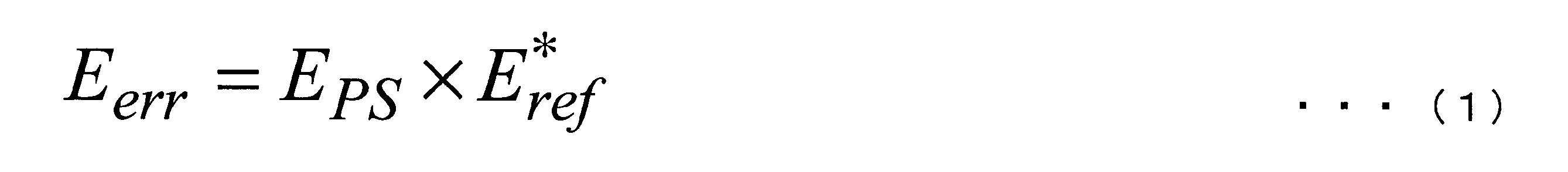
- the reference pilot symbol storage unit 442 stores pilot symbols inserted by the pilot symbol insertion unit 121 of the transmission apparatus 1 as reference symbols. Based on the reference symbol (E ref ) stored in the reference pilot symbol storage unit 442 and the pilot symbol (E PS ) extracted by the pilot symbol detection unit 441, the error signal calculation unit 443 is a complex electric field error signal. Is calculated. The error signal calculation unit 443 outputs the calculated complex electric field error signal to the compensation electric field signal generation unit 444. The calculation of the complex electric field error signal (E err ) is performed using, for example, the following equation (1). Note that E ref * in Equation (1) is a complex conjugate value of the reference symbol (E ref ).
- the compensation electric field signal generation unit 444 estimates phase noise of data between pilot symbols in the received complex electric field signal based on the complex electric field error signal calculated by the error signal calculation unit 443.
- FIG. 7 is a block diagram illustrating a configuration of the compensation electric field signal generation unit 444 in the present embodiment.
- the compensation electric field signal generation unit 444 includes a first amplitude normalization unit 4441, an interpolation processing unit 4442, and a second amplitude normalization unit 4445.
- the amplitude of the complex electric field error signal input to the compensation electric field signal generation unit 444 is the amplitude of the reference symbol (E ref ) of the reference pilot symbol storage unit 442 and the pilot symbol (E PS ) extracted by the pilot symbol detection unit 441.
- the first amplitude normalization unit 4441 detects the amplitude value of the input complex electric field error signal.
- the first amplitude normalization unit 4441 normalizes the complex electric field error signal by multiplying the complex electric field error signal by the reciprocal of the detected amplitude value, and sets the amplitude of the complex electric field error signal to 1.
- the first amplitude normalization unit 4441 outputs the normalized complex electric field error signal to the interpolation processing unit 4442.
- the first amplitude normalization unit 4441 By the normalization performed by the first amplitude normalization unit 4441, the amplitude dependency of reference symbols having different amplitude values can be removed. However, when a pilot symbol having a constant amplitude is inserted in the transmission apparatus 1, the first amplitude normalization unit 4441 may be omitted. In this case, the calculation amount and circuit scale in the compensation electric field signal generation unit 444 can be suppressed.
- the first amplitude normalization unit 4441 since the first amplitude normalization unit 4441 is used for adjusting the amplitude of the complex electric field error signal, it may be other than the above-described calculation, for example, multiplying the reciprocal of the square of the amplitude of the reference symbol (E ref ). Thus, the amplitude of the complex electric field error signal may be normalized so as to be the ratio of the pilot symbol (E PS ) to the reference symbol (E ref ), or when the normalization calculation is not performed, the first amplitude standard The converting unit 4441 may be omitted. In the present embodiment, a case where the amplitude of the complex electric field error signal is normalized to 1 will be described.
- the interpolation processing unit 4442 includes a complex electric field interpolation unit 4443 and a low-pass filter 4444.
- the complex electric field error signal normalized from the first amplitude normalization unit 4441 is input to the complex electric field interpolation unit 4443.
- the complex electric field interpolation unit 4443 duplicates and inserts the value of the complex electric field error signal corresponding to the pilot symbol position close to each symbol position or zero between the input complex electric field error signals. That is, the complex electric field interpolation unit 4443 performs zero padding or replica insertion on a symbol interval between complex electric field error signals existing for each K symbol.
- the complex electric field interpolation unit 4443 inputs a symbol string generated by inserting zeros or duplicate values into symbols between complex electric field error signals, and inputs the low-pass filter 4444.
- FIG. 8 is a diagram illustrating an example of a signal (a symbol string input to the low-pass filter 4444) generated by the complex electric field interpolation unit 4443 in the present embodiment.
- the horizontal axis indicates time (symbol). Symbols are interpolated between complex electric field error signals (E err 1-1, E err 1-2,...) That exist for each K symbol.
- the low-pass filter 4444 performs processing to pass a predetermined frequency component included in the symbol string input from the complex electric field interpolation unit 4443. By this processing, the data part between the complex electric field error signals can be interpolated, and the phase noise of the data part located between the pilot symbols in the received complex electric field signal can be estimated.
- the pilot symbol insertion interval is T [SEC]
- the low-pass filter 4444 sets the cutoff frequency F [Hz] to (1) so that the phase noise of (1 / 2T) [Hz] can be estimated.
- / 2T) A frequency that is less than [Hz] (F ⁇ (1 / 2T)).
- the low-pass filter 4444 inputs the symbol sequence obtained by the above filter processing to the second amplitude normalization unit 4445 as a phase noise sequence.
- the second amplitude normalization unit 4445 normalizes the amplitude of each symbol of the input phase noise series.
- the amplitude normalization performed by the second amplitude normalization unit 4445 is a process of setting the amplitude of each symbol of the input phase noise series to 1.
- the second amplitude normalization unit 4445 inputs the normalized phase noise sequence to the phase compensation unit 445 as a compensation electric field signal.
- FIG. 9 is a block diagram showing a configuration example of the low-pass filter 4444 in the present embodiment.
- K is a pilot symbol interval.
- the figure shows an example in which a symbol of a data portion is interpolated using a low-pass filter (LPF) having M taps.
- LPF low-pass filter
- the operation speed of the preceding stage of the low-pass filter can be reduced to 1 / K, and the circuit scale can be further reduced. it can.
- the phase compensation unit 445 receives the received complex electric field signal tapped before the pilot symbol detection unit 441 and the compensation electric field signal from the second amplitude normalization unit 4445 of the compensation electric field signal generation unit 444.
- the phase compensation unit 445 calculates a complex conjugate value of the compensation electric field signal, and performs complex multiplication on the received complex electric field signal with the calculated complex conjugate value. Thereby, the phase noise of the data part estimated using the pilot symbol can be compensated.
- the phase noise compensation unit 44 in this embodiment can compensate for phase noise by directly calculating the phase angle of the complex electric field error signal by normalization and complex multiplication. Therefore, the phase noise compensation unit 44 has a configuration for calculating the phase angle, for example, a memory (table) that stores the phase angle corresponding to the values of the in-phase component and the quadrature component of the complex electric field error signal, and the memory. There is no need to provide a configuration for reference. Thereby, the configuration of the phase noise compensation unit 44 can be simplified, and the circuit scale can be reduced when the phase noise compensation unit 44 is mounted on a circuit or the like.
- the unwrap process is a process of calculating a target phase angle by limiting the phase difference between the target symbol and the previous symbol so as not to exceed the range of ⁇ ⁇ .
- phase noise compensation unit 44 By using the phase noise compensation unit 44 having the above-described configuration, phase fluctuations occurring in the transmission apparatus 1, the optical fiber transmission line 2, and the reception apparatus 3 are estimated, and phase compensation is performed on the data to thereby achieve phase synchronization. Can be established and communication quality can be improved.
- FIG. 10 is a graph showing quality (Q value) improvement by the phase noise compensation unit 44 of the present embodiment.
- the horizontal axis indicates the residual frequency offset
- the vertical axis indicates the Q value.
- the residual frequency offset indicates the frequency offset remaining in the received complex electric field signal.
- the figure shows the Q values when the processing by the phase noise compensation unit 44 is performed (with phase compensation) and when the processing is not performed (without phase compensation).
- the Q value is lowered when the residual frequency offset exceeds 10 [MHz], whereas the phase compensation is performed to prevent the Q value from being lowered due to the increase of the residual frequency offset.
- the frequency offset tolerance can be improved.
- the interpolation processing unit in the second embodiment performs processing without performing interpolation on the data portion between the complex electric field error signals.
- FIG. 11 is a block diagram illustrating a configuration of the interpolation processing unit 5442 in the second embodiment.
- the interpolation processing unit 5442 includes a low-pass filter 5443 and a linear interpolation processing unit 5444.
- the low-pass filter 5443 receives the complex electric field error signal normalized from the first amplitude normalization unit 4441.
- the low-pass filter 5443 performs processing to pass a predetermined frequency component included in the input complex electric field error signal. By this processing, the complex electric field error signal is averaged.
- the linear interpolation processing unit 5444 calculates the phase noise of the data part by linear interpolation using the complex electric field error signal averaged by the low-pass filter 5443.
- the linear interpolation processing unit 5444 inputs a phase noise sequence including the averaged complex electric field error signal and the calculated phase noise of the data portion to the second amplitude normalization unit 4445.
- FIG. 12 is a diagram illustrating an example of a complex electric field error signal input to the low-pass filter 5443 in the present embodiment.
- the horizontal axis indicates time (symbol).
- the signal input to the low-pass filter 5443 is a signal composed of a complex electric field error signal.
- FIG. 13 is a block diagram illustrating a configuration example of the low-pass filter 5443 in the present embodiment.
- K is a pilot symbol interval.
- This figure shows an example in which an average value is calculated from M complex electric field error signals using a low-pass filter with M taps, and phase noise of the data portion is calculated based on the calculated average value.
- the cut-off frequency F [Hz] of the phase noise estimated by the pilot symbol is sufficiently smaller than 1 / (2T) [Hz] that is the frequency of the phase noise that can be estimated by the pilot symbol
- the low-pass frequency in the first embodiment The tap coefficients of the low-pass filter used as the filter 4444 and the low-pass filter used as the low-pass filter 5443 are substantially equivalent values.
- the circuit scale of the low-pass filter is suppressed to 1 / K and the phase noise interpolation accuracy in the data portion is improved. be able to.
- FIG. 14 is a graph showing the communication quality (Q value) in the first embodiment and the second embodiment.
- the horizontal axis indicates the residual frequency offset
- the vertical axis indicates the Q value.
- the configuration of the low-pass filter used as the low-pass filter 5443 includes a data portion for linear interpolation using the value of the complex electric field error signal and the output of the low-pass filter from the viewpoint of interpolation accuracy and circuit scale in the linear interpolation processing unit 5444. May be used to determine the data portion to be linearly interpolated to further reduce the circuit scale of the low-pass filter.
- FIG. 15 is a block diagram illustrating a configuration of the compensation electric field signal generation unit 644 in the third embodiment.
- the compensation electric field signal generation unit 644 includes a phase difference calculation unit 6441, an interpolation processing unit 6442, and a phase electric field conversion unit 6443.
- the complex electric field error signal calculated by the error signal calculation unit 443 is input to the phase difference calculation unit 6441.
- the phase difference calculator 6441 calculates the phase component of the input complex electric field error signal.
- phase angle corresponding to the combination of the in-phase component value and the quadrature component value is provided in advance, and the in-phase component is orthogonal
- the phase angle corresponding to the component is read out.
- the phase angle may be calculated using the following equation (2) that is an approximate equation of the phase relationship when the phase is sufficiently small.
- J is an imaginary unit.
- the phase difference calculation unit 6441 performs unwrap processing in order to achieve continuity with the phase angle calculated one time before the calculated phase angle ( ⁇ err ). In general unwrap processing, conditional branching occurs because the magnitude of phase change is determined to remove phase uncertainty. This increases the circuit scale. If (2 ⁇ WT ⁇ ) 1 holds when the phase variation to be compensated is W [Hz], the difference between the phase of the complex electric field error signal one time before and the phase of the current complex electric field error signal (Phase difference) is sufficiently small. In this case, the phase difference calculation unit 6441 can be configured as shown in FIG.
- FIG. 16 is a block diagram illustrating a configuration example of the phase difference calculation unit 6441 in the present embodiment.
- the phase difference calculation unit 6441 includes a delay unit 6445, a subtracter 6446, a phase difference calculator 6447, and an adder 6448.
- the complex electric field error signal input to the phase difference calculation unit 6441 is input to the delay unit 6445 and the subtractor 6446.
- the delay unit 6445 delays the input complex electric field error signal by one time, and then outputs the complex electric field error signal to the subtracter 6446 and the adder 6448.
- the subtractor 6446 subtracts the complex electric field error signal output from the delay unit 6445 from the input complex electric field error signal, and outputs the subtraction result to the phase difference calculator 6447.
- the phase difference calculator 6447 calculates the phase by using the expression (2) with the subtraction result output from the subtractor 6446 as E err .
- the phase difference calculator 6447 outputs a complex signal indicating the calculated phase to the adder 6448.
- the adder 6448 adds the complex electric field error signal output from the delay unit 6445 and the complex signal output from the phase difference calculator 6447, and outputs the addition result to the interpolation processing unit 6442.
- the phase difference calculating unit 6441 can realize the calculation of the phase difference and the unwrapping process with the above configuration.
- the interpolation processing unit 6442 has a phase difference corresponding to zero or a pilot symbol position close to the symbol position at a symbol position corresponding to the data portion, which is a symbol between complex electric field error signals corresponding to the pilot symbol position. Insert a value.
- a signal of a symbol string obtained by inserting zero or a phase difference into symbols between phase differences is input to a low-pass filter to estimate phase noise corresponding to the data portion.
- the phase difference is input to the low-pass filter, the average value of the phase difference is calculated, and the phase noise corresponding to the data portion is estimated by linear interpolation.
- the interpolation processing unit 6442 performs the same processing as the interpolation processing unit 4442 in the first embodiment or the interpolation processing unit 5442 in the second embodiment on the phase difference output from the phase difference calculation unit 6441.
- the phase electric field converter 6443 outputs the complex signal obtained by the conversion to the phase compensator 445 as a compensation electric field signal.
- the transmission apparatus 1 intermittently inserts pilot symbols, which are known signals, into the data and transmits the data, and the reception apparatus 3 adds the pilot symbol from the received signal.
- a pilot symbol is extracted, and phase fluctuations occurring in the transmitter 1, the optical fiber transmission line 2, and the receiver 3 are estimated using the difference between the pilot symbol (reference symbol) before transmission and the pilot symbol after transmission.
- Phase compensation is performed on the data.
- the configuration in which the reception device 3 includes the phase noise compensation unit has been described.
- the relay device or the like may include a phase noise compensation unit, or an apparatus that performs phase compensation in the optical transmission system.
- a phase noise compensation unit may be provided.
- FIG. 17 is a block diagram showing a configuration of the compensation electric field signal generation unit 744 in the present embodiment.
- the compensation electric field signal generation unit 744 includes a first amplitude normalization unit 7441 and an interpolation processing unit 7442.
- the interpolation processing unit 7442 includes a low-pass filter 7443, a first linear interpolation processing unit 7444, a second amplitude normalization unit 7445, and a second linear interpolation processing unit 7446.
- the first amplitude normalization unit 7441 and the low-pass filter 7443 are the same as those in the second embodiment, and an averaged complex electric field error signal is output from the low-pass filter 7443.
- the first linear interpolation processing unit 7444 is averaged complex electric field error signal (hereinafter, referred to as E current) and the complex electric field error signal (hereinafter outputted from low-pass filter 7443 just before the E current, E previous previous And a phase interval of the data portion located at the boundary of each interval is calculated by linear interpolation using E previous and E current. .
- FIG. 18 illustrates the calculated position of the phase noise.
- the horizontal axis represents time (symbol).
- the amplitude of the complex signal indicating the calculated phase noise and E previous and E current is normalized by the second amplitude normalization unit 7445.
- the second linear interpolation processing unit 7446 calculates the phase noise of the data portion located in the section by linear interpolation using the standardized E previous , E current , and phase noise.
- E itp1 , E itp2 , and E itp3 are phase noises of data portions located at the boundaries of each section divided for each K / 4 symbol.
- E itp1 , E itp2 , and E itp3 are calculated in the first linear interpolation processing unit 7444 according to , for example, Expression (3), Expression (4), and Expression (5).
- E previous to E itp1 are referred to as the first interval
- E itp1 to E itp2 are referred to as the second interval
- E itp2 to E itp3 are referred to as the third interval
- E itp3 to E current are referred to as the fourth interval.
- the boundary points of each section, E itp1 , E itp2 , E itp3 , E previous , and E current are each normalized by the second amplitude normalization unit 7445.
- the normalized E itp1 , E itp2 , E itp3 , E previous , and E current exist on the unit circumference in the complex plane, as shown in FIG. 19B.
- the second linear interpolation processing unit 7446 calculates the phase noise of the data portion in the first section by linear interpolation using the normalized E previous and E itp1 .
- the calculation of the phase noise of the data portion in the second to fourth sections is the same, and the phase noise of the data portion in the second to fourth sections is calculated by linear interpolation using the boundary points of each section after normalization. .
- the value of the phase noise of the data portion in each section approximates to a unit circle in the complex plane as shown in FIG. 19C. That is, the phase noise sequence including the averaged complex electric field error signal and the phase noise of the data portion is approximately present on the unit circumference, and is the same as in the second embodiment in which all the phase noise sequences are normalized. An effect can be obtained.
- the circuit scale of the second amplitude normalization unit 7445 can be suppressed to (W + 1) / K. it can.
- FIG. 20 is a block diagram illustrating a configuration of the compensation electric field signal generation unit 844 in the present embodiment.
- the compensation electric field signal generation unit 844 includes a first amplitude normalization unit 8441 and an interpolation processing unit 8442.
- the interpolation processing unit 8442 includes a low-pass filter 8443, a first linear interpolation processing unit 8444, a second amplitude normalization unit 8445, a second linear interpolation processing unit 8446, a residual frequency offset estimation unit 8447, a complex conjugate calculation unit 8448, and multiplication.
- the first amplitude normalization unit 8441, the low-pass filter 8443, the first linear interpolation processing unit 8444, the second amplitude normalization unit 8445, and the second linear interpolation processing unit 8446 are the compensation electric field signal generation unit illustrated in FIG. It is the same structure as the corresponding component in 744.
- the residual frequency offset estimation unit 8447 estimates the residual frequency offset from the complex electric field error signal output from the first amplitude normalization unit 8441. With this configuration, it is possible to estimate the residual frequency offset and phase noise separately, improving the estimation accuracy, and designing the bandwidth of the low-pass filter 8443 by paying attention to the fluctuation band of the phase noise. It becomes possible.
- FIG. 21 shows an example of the configuration of the residual frequency offset estimation unit 8447.
- the residual frequency offset estimation unit 8447 only needs to be able to estimate the residual frequency offset from the complex electric field error signal output from the first amplitude normalization unit 8441.
- the residual frequency offset estimation unit 8447 is of a high-order PLL (Phase Locked Loop) type (not shown). A configuration may be taken.
- PLL Phase Locked Loop
- the residual frequency offset estimation unit 8447 includes a slope detection unit 8500 (phase slope detection unit), a low-pass filter 8510, an electric field phase conversion unit 8520, an integration unit 8530, and a phase electric field conversion unit 8540.
- the slope detection unit 8500 includes a delay unit 8501, a complex conjugate calculation unit 8502, a multiplier 8503, and a multiplier 8504.
- the integration unit 8530 includes an adder 8531 and a delay unit 8532.
- the slope detection unit 8500 in FIG. 21 calculates an instantaneous value of the residual frequency offset.
- the complex electric field error signal input to the slope detection unit 8500 is supplied to a delay unit 8501, a multiplier 8503, and a multiplier 8504.
- the delay unit 8501 gives a delay of one time to the input complex electric field error signal, and then outputs the delayed complex electric field error signal to the complex conjugate calculation unit 8502.
- the complex conjugate calculation unit 8502 calculates a complex conjugate value of the input complex electric field error signal, and outputs the calculated complex conjugate value to the multiplier 8503 and the multiplier 8504.
- Multipliers 8503 and 8504 are for the normalized complex electric field error signal input from first amplitude normalization unit 8441 (FIG. 20) and the previous complex electric field error signal output from complex conjugate calculation unit 8502.
- the complex conjugate value is multiplied to calculate the fluctuation amount of the complex electric field in the pilot symbol interval T [sec].
- the calculated fluctuation amount of the complex electric field is input to the low-pass filter 8510 and averaged.
- the bandwidth of the low-pass filter 8510 may be designed based on the bandwidth of time fluctuation of the residual frequency offset and the noise level included in the complex electric field error signal.
- the electric field phase converter 8520 converts the complex electric field value output from the low-pass filter 8510 into a phase value [rad].
- the electric field phase conversion unit 8520 can mitigate arithmetic deterioration of the integration unit 8530 described later.
- the converted phase value is input to integration unit 8530.
- the adder 8531 adds the output of the electric field phase conversion unit 8520 to the output of the previous integration unit 8530 output from the delay unit 8532 in order to integrate the phase values.
- the integration unit 8530 can ensure the continuity of the phase change of the estimated residual frequency offset.
- the output of the electric field phase conversion unit 8520 is processed by a 2 ⁇ [rad] modulo calculation unit (not shown), and the output of the integration unit 8530 is changed from ⁇ to + ⁇ ( Alternatively, it may be limited to 0 to + 2 ⁇ ).
- the integration value output from the integration unit 8530 is input to the phase electric field conversion unit 8540 as a phase value, and is converted again to a complex electric field value. That is, the phase electric field conversion unit 8540 converts the output of the integration unit 8530 into a complex electric field error signal that is an input format to the first linear interpolation processing unit 8444 of the interpolation processing unit 8442.
- the complex electric field error signal output from the residual frequency offset estimation unit 8447 is converted into a complex conjugate value by the complex conjugate calculation unit 8448.
- the multiplier 8449 and the multiplier 8450 multiply the normalized complex electric field error signal output from the first amplitude normalization unit 8441 and the converted complex conjugate value, and the multiplication result is a low-pass filter 8443. To enter. By this multiplication, the residual frequency offset component is removed from the complex electric field error signal input to the low-pass filter 8443.
- the bandwidth of the low-pass filter 8443 at the subsequent stage is set to the bandwidth of the phase noise component. Since the output of the low-pass filter 8443 is only the phase noise estimation value, the output of the low-pass filter 8443 and the output result of the residual frequency offset estimation unit 8447 are multiplied by the multiplier 8451 and the multiplier 8252 to obtain the residual frequency offset.
- a complex electric field error signal including a component and a phase noise component is generated.
- the generated complex electric field error signal is input to the first linear interpolation processing unit 8444. Thereafter, the same processing as in the fourth embodiment is performed.
- FIG. 22 shows a frame structure of a transmission / reception frame in the sixth embodiment.
- the same signals as those shown in FIG. 3 are denoted by the same reference numerals.
- FIG. 23 is a block diagram showing a configuration of the residual frequency offset estimation unit 9447 in the present embodiment.
- the residual frequency offset estimation unit 9447 includes a slope detection unit 9500, a low-pass filter 9510, an electric field phase conversion unit 9520, an integration unit 9530, a phase electric field conversion unit 9540, and a coefficient setting unit 9550.
- the slope detection unit 9500 includes a delay unit 9501, a complex conjugate calculation unit 9502, a multiplier 9503, and a multiplier 9504.
- the integration unit 9530 includes an adder 9531 and a delay unit 9532.
- the components other than the coefficient setting unit 9550 are the same as the corresponding components in the residual frequency offset estimation unit 8447 shown in FIG.
- a synchronization pattern (for example, synchronization pattern TS1) composed of consecutive symbols having the above frame structure includes pilot symbols.
- a pilot symbol having a symbol length of 1 is inserted for each L symbol (PSA-1, PSA-2,..., PSA-n in the figure).
- pilot symbol detection section 441 shown in FIG. 5 detects pilot symbols included in the synchronization pattern and pilot symbols included in the data.
- pilot symbol extraction units 4413 and 4414 in FIG. 6 extract pilot symbols included in the synchronization pattern and pilot symbols included in the data.
- the extracted pilot symbols are input to the compensation electric field signal generation unit 844 in FIG. 20 and are normalized by the first amplitude normalization unit 8441.
- the normalized complex electric field error signal is input to the interpolation processing unit 8442 in FIG.
- the residual frequency offset estimation unit 9447 illustrated in FIG. 23 includes a coefficient setting unit 9550.
- a method for estimating a residual frequency offset only with pilot symbols included in data will be described. If the residual frequency offset is ⁇ [Hz] and the output of the electric field phase conversion unit 9520 for the complex electric field error signal using the pilot symbol included in the data is ⁇ (n) [rad], the relationship with ⁇ is Equation (6) is obtained.
- the pilot symbol insertion interval in the data interval is T [sec], and it is assumed that a pilot symbol is inserted every K symbols.
- the output ⁇ (n) of the electric field phase conversion unit 9520 for the synchronization pattern satisfies Expression (7) in order to convert the residual frequency offset estimated by the pilot symbol included in the data into the residual frequency offset for the synchronization pattern.
- the estimated value of the residual frequency offset with respect to the synchronization pattern is obtained by the coefficient setting unit 9550 shown in FIG. 23 with respect to the output ⁇ (n) of the electric field phase conversion unit 9520 for the complex electric field error signal using the pilot symbol included in the data. , L / K times to obtain a value.
- Residual frequency offset can be compensated for intervals and sync patterns.
- the seventh embodiment a configuration of mapping on the complex plane of the synchronization pattern will be described.
- the synchronization pattern any pattern may be used as long as the receiving apparatus 3 in FIG. 1 can detect the correlation peak when detecting the synchronization pattern in the received digital signal.
- PRBS Pulseudo Random Bit Sequence
- PRBS has a sharp correlation only when the delay becomes zero. Note that PRBS is the same as PN sequence and M sequence.
- FIG. 24 shows a mapping example on the complex plane of the synchronization pattern in the symbol mapping unit 123 in FIG.
- the symbols shown in the figure are those when 16 QAM (QAM: “Quadrature” Amplitude ”Modulation) is adopted as a modulation method.
- the symbol mapping unit 123 maps to the symbol ( ⁇ ) filled in black among the 16 symbols shown in FIG. This is to prevent the synchronization pattern from receiving excessive phase noise compared to the data signal due to noise during transmission and waveform distortion.
- phase noise that may occur during transmission are the non-linear optical effects of self-phase modulation (SPM: Self-Phase Modulation), cross-phase modulation (XPM: Cross-Phase Modulation), and local light (LO: Local Oscillator).
- SPM Self-Phase Modulation
- XPM Cross-Phase Modulation
- LO Local Oscillator
- FIG. 25 is a diagram illustrating a configuration example of a transmission / reception frame including a synchronization pattern in which mapping is performed on the same complex plane.
- BPSK Binary Phase Shift Shift Keying
- the symbol mapping unit 123 in FIG. 2 grasps the position of the pilot symbol inserted by the pilot symbol insertion unit 121 and the position of the synchronization pattern inserted by the synchronization pattern insertion unit 122, and the mapping target is the pilot symbol, synchronization pattern, data
- the symbol to be mapped is selected according to which of the signals. For example, when mapping a synchronization pattern when 64QAM is used as a modulation scheme, the symbol mapping unit 123 selects two symbols from 64 symbols, and the mapping result to the selected symbol becomes a PRBS pattern. Like that. Further, the bit pattern obtained as PRBS may be multiplied by 6 and mapped using 64QAM.
- a convolution circuit that performs a convolution operation can be used to calculate the correlation in the synchronization pattern detection unit 4412 of FIG.
- the input to the convolution circuit is a received digital signal and a known synchronization pattern.
- the time position may be detected by binary identification of the received digital signal and specifying the time position where the digital pattern and the synchronization pattern substantially match. As a result, the circuit scale of the synchronization pattern detection unit 4412 can be reduced.
- differential detection and exclusive OR operation can be used in place of the convolution operation.
- a steady frequency offset component can be removed.
- the phase of the synchronization pattern when the frequency offset occurs is ⁇ ( ⁇ (1) + ⁇ N (1)), ( ⁇ (2) + ⁇ N (2)),..., ( ⁇ (N) + ⁇ N (N)) ⁇ It can be expressed.
- ⁇ N (n + 1) ⁇ N (n) is in the range of ⁇ to + ⁇ , and the time variation of the frequency offset is small.
- ⁇ N (n + 1) ⁇ N (n) has a substantially constant value and can be removed. Therefore, the differential detection component does not have the phase rotation component due to the frequency offset, and only the ⁇ (1),..., ⁇ (N ⁇ 1) components can be extracted.
- FIG. 26 is a block diagram illustrating a configuration example of the synchronization pattern detection unit 1004A at the time of differential detection.
- a configuration will be described in which phase information is used as a synchronization pattern and a modulation scheme having information of two bits or more in one symbol is used.
- As a modulation method in this case for example, there is QPSK (Quadrature Phase Shift Keying) modulation.
- the synchronization pattern detection unit 1004A includes a differential detection unit 1041, an identification unit 1042, and a pattern synchronization unit 1044. Further, a reference synchronization pattern storage unit 1043 corresponding to the reference synchronization pattern storage unit 4411 shown in FIG. 6 is connected to the synchronization pattern detection unit 1004A.
- the differential detection unit 1041 receives an I signal component and a Q signal component that are signals corresponding to the horizontal axis (in-phase component) and the vertical axis (orthogonal component) on the complex plane.
- the differential detection unit 1041 calculates a differential detection signal by time-synchronizing the I signal component and the Q signal component.
- the identification unit 1042 performs determination on the complex plane with respect to the differential detection signal calculated by the differential detection unit 1041, and performs demapping and decoding.
- the identification unit 1042 sequentially outputs signals obtained by decoding.
- the reference synchronization pattern storage unit 1043 stores in advance a reference signal generated based on the synchronization pattern as an expected value of the synchronization pattern.
- the pattern synchronization unit 1044 acquires synchronization position information by performing position synchronization between the synchronization pattern code sequence sequentially output from the identification unit 1042 and the reference signal stored in the reference synchronization pattern storage unit 1043.
- FIG. 27 is a block diagram illustrating a configuration example of the differential detection unit 1041 in the present embodiment.
- the differential detection unit 1041 includes delay units 1411 and 1412, a complex conjugate calculation unit 1413, and a complex multiplication unit 1414.
- the I signal component input to the differential detection unit 1041 is input to the delay unit 1411 and the complex multiplication unit 1414.
- the delay unit 1411 gives a delay of one symbol to the I signal component, and then outputs it to the complex conjugate calculation unit 1413.
- the Q signal component input to the differential detection unit 1041 is input to the delay unit 1412 and the complex multiplication unit 1414.
- the delay unit 1412 gives a delay of one symbol to the Q signal component, and then outputs it to the complex conjugate calculation unit 1413.
- the complex conjugate calculation unit 1413 calculates a complex conjugate signal with respect to a complex signal obtained using the input from the delay unit 1411 as an in-phase component and the input from the delay unit 1412 as a quadrature component.
- the complex conjugate calculator 1413 outputs the calculated complex conjugate signal to the complex multiplier 1414.
- the complex multiplier 1414 multiplies the complex signal composed of the I signal component and the Q signal component by the complex signal calculated by the complex conjugate calculator 1413, and outputs the multiplication result as a differential detection signal.
- the multiplication in the complex multiplier 1414 is expressed by the following equation (9).
- Equation (9) E I (t) corresponds to a complex signal input from the outside to the complex multiplier 1414, and E I (t ⁇ 1) * is input from the complex conjugate calculator 1413 to the complex multiplier 1414.
- E I (t) the amplitude value
- the output of the complex multiplier 1414 is only the phase component.
- amplitude noise occurs due to transmission and the amplitude value deviates from 1
- only the phase information can be obtained by dividing and normalizing the output of the complex multiplier 1414 by the amplitude value of the output.
- Position synchronization between the synchronization pattern code sequence and the reference signal in the pattern synchronization unit 1044 is performed by an exclusive OR operation with the reference signal for the synchronization pattern code sequence output from the identification unit 1042.
- the target of exclusive OR operation with the reference signal in the synchronization pattern code sequence output from the identification unit 1042 is identical with the reference signal, the result of the exclusive OR operation is 0 for the synchronization pattern length.
- the target of exclusive OR operation with the reference signal matches the reference signal, 1 continues for the synchronization pattern length. You can also The same can be realized by providing an inverting circuit for the result of the exclusive OR operation.
- FIG. 28 is a block diagram illustrating a configuration example of a synchronization pattern detection unit 1004B as a modification of the synchronization pattern detection unit in the present embodiment.
- the synchronization pattern detection unit 1004A shown in FIG. 26 the configuration in the case where a modulation scheme having information of 2 bits or more in one symbol is used for the synchronization pattern has been described.
- the synchronization pattern detection unit 1004B has a configuration when a modulation scheme having 1 symbol of 1 bit information is used for a synchronization pattern.
- the modulation method includes BPSK.
- the synchronization pattern detection unit 1004B includes a differential detection unit 1041, an identification unit 1042B, and a pattern synchronization unit 1044B. Further, a reference synchronization pattern storage unit 1043B corresponding to the reference synchronization pattern storage unit 4411 shown in FIG. 6 is connected to the synchronization pattern detection unit 1004B.
- the differential detection unit 1041 has the same configuration as the differential detection unit 1041 shown in FIG.
- the I signal component of the differential detection signal calculated by the differential detection unit 1041 is input to the identification unit 1042B.
- the identification unit 1042B performs determination on the complex plane with respect to the differential detection signal, and performs demapping and decoding.
- the identification unit 1042B sequentially outputs signals obtained by decoding.
- a reference signal generated based on the synchronization pattern is stored in advance as an expected value of the synchronization pattern.
- the pattern synchronization unit 1044B acquires the synchronization position information by performing position synchronization between the synchronization pattern code sequence sequentially output from the identification unit 1042B and the reference signal stored in the reference synchronization pattern storage unit 1043B.
- the I signal component output from the differential detection unit 1041 is input to the identification unit 1042B.
- the output of the identification unit 1042B receives the I signal component or the Q signal component if inversion is allowed.
- the input to the identification unit 1042B may be any.
- FIG. 29A and FIG. 29B are diagrams showing examples of mapping of the synchronization pattern when the data signal is modulated by 32QAM and 64QAM.
- symbols used for synchronization pattern mapping are painted black.
- an example in which the synchronization pattern is mapped as QPSK is shown.
- symbols other than the symbol having the maximum amplitude value and the minimum amplitude value are assigned to the synchronization pattern so that errors are not easily generated. This is because an error is likely to occur in the symbol having the smallest amplitude value due to the influence of noise, and an error is likely to occur in the symbol having the largest amplitude value due to the influence of the nonlinear optical effect.
- mapping shown in FIGS. 29A and 29B is an example, and mapping using symbols different from those shown in FIG. 29A may be performed.
- mapping the synchronization pattern as BPSK two symbols that are 180 ° out of phase are selected from the symbols ( ⁇ ) filled in black.
- the synchronization pattern repeatedly arrives at the cycle of the symbol length of the transmission / reception frame. Therefore, the synchronization position of each frame is averaged to improve detection sensitivity. be able to.
- Other processing may be performed in the same manner as in the first to sixth embodiments.
- a program for realizing the function of each unit (for example, the phase noise compensation unit) in the above embodiment is recorded on a computer-readable recording medium, and the program recorded on the recording medium is read into a computer system. , Processing of each unit (for example, phase compensation) may be performed.
- the “computer system” includes hardware such as an OS (Operating System) and peripheral devices.
- the “computer system” also includes a WWW (World Wide Web) system provided with a homepage providing environment (or display environment).
- “Computer-readable recording medium” means a portable medium such as a flexible disk, a magneto-optical disk, a ROM (Read Only Memory), a CD (Compact Disk) -ROM, or a hard disk built in a computer system.
- the “computer-readable recording medium” means a volatile memory (RAM (Random Access) inside a computer system that becomes a server or a client when a program is transmitted via a network such as the Internet or a communication line such as a telephone line. Memory)) as well as those that hold programs for a certain period of time.
- RAM Random Access
- the program may be transmitted from a computer system storing the program in a storage device or the like to another computer system via a transmission medium or by a transmission wave in the transmission medium.
- the “transmission medium” for transmitting the program refers to a medium having a function of transmitting information, such as a network (communication network) such as the Internet or a communication line (communication line) such as a telephone line.
- the program may be for realizing a part of the functions described above. Further, the program may be a so-called difference file (difference program) that can realize the above-described functions in combination with a program already recorded in the computer system.
- the present invention is applicable to, for example, an optical transmission system. According to the present invention, it is possible to perform phase compensation by acquiring phase fluctuations in a received complex electric field signal without calculating a phase angle related to signals between pilot symbols and performing continuity processing for phase fluctuations. In addition, the circuit scale can be reduced.
- Pilot symbol detection unit 442 ... Reference pilot symbol storage unit 443 ... Error signal calculation units 444, 644, 744, 844 ... Compensation Electric field signal generation unit 445 ... phase compensation units 1004A, 1004B ... synchronization pattern detection 1041... Differential detection units 1042 and 1042B... Identification units 1043 and 1043B... Reference synchronization pattern storage units 1044 and 1044B... Pattern synchronization units 1411 and 1412. Storage unit 4412 ... Synchronization pattern detection units 4413 and 4414 ... Pilot symbol extraction units 4441, 7441 and 8441 ... First amplitude normalization units 4442, 5442, 6442, 7442 and 8442 ... Interpolation processing unit 4443 ...
Landscapes
- Engineering & Computer Science (AREA)
- Computer Networks & Wireless Communication (AREA)
- Signal Processing (AREA)
- Physics & Mathematics (AREA)
- Electromagnetism (AREA)
- Optical Communication System (AREA)
- Digital Transmission Methods That Use Modulated Carrier Waves (AREA)
Abstract
Description
本願は、2013年2月13日に日本へ出願された特願2013-025924号に基づき優先権を主張し、その内容をここに援用する。 The present invention relates to an optical transmission system, a phase compensation method, and an optical receiving apparatus that improve communication quality by compensating phase noise generated on a transmission side, a reception side, and a transmission path in an optical transmission system.
This application claims priority based on Japanese Patent Application No. 2013-025924 for which it applied to Japan on February 13, 2013, and uses the content here.
図1は、第1の実施形態における光伝送システムの構成例を示すブロック図である。光伝送システムは、デジタルコヒーレント伝送方式によるデータの伝送を行う送信装置1、光ファイバ伝送路2、及び、受信装置3を具備している。送信装置1は、送信すべきデータを含む変調光を生成し、生成した変調光を光ファイバ伝送路2に出力する。送信装置1から出力される変調光は、光ファイバ伝送路2を伝播する。受信装置3は、光ファイバ伝送路2を伝播した変調光を受信し、受信した変調光からデータを取得する。 (First embodiment)
FIG. 1 is a block diagram illustrating a configuration example of an optical transmission system according to the first embodiment. The optical transmission system includes a
受信装置3は、局発光源31、偏波多重光ハイブリッド32、バランス検波器33a~33d、アナログデジタル変換器(ADC)34a~34d、及び、デジタル信号処理部4を備えている。局発光源31はCW光を生成し、生成したCW光を偏波多重光ハイブリッド32に出力する。偏波多重光ハイブリッド32には、受信した変調光とCW光とが入力される。偏波多重光ハイブリッド32は、CW光を用いたコヒーレント検波により、変調光の同相成分及び直交成分の光信号を検出する。偏波多重光ハイブリッド32は、検出した同相成分及び直交成分の光信号をバランス検波器33a~33dに出力する。 Returning to FIG. 1, the description of the configuration of the optical transmission system will be continued.
The receiving
参照パイロットシンボル記憶部442には、送信装置1のパイロットシンボル挿入部121により挿入されるパイロットシンボルが参照シンボルとして記憶されている。誤差信号演算部443は、参照パイロットシンボル記憶部442に記憶されている参照シンボル(Eref)と、パイロットシンボル検出部441において抽出されたパイロットシンボル(EPS)とに基づいて、複素電界誤差信号を算出する。誤差信号演算部443は、算出した複素電界誤差信号を補償電界信号生成部444に出力する。複素電界誤差信号(Eerr)の算出は、例えば、次式(1)を用いて行われる。なお、式(1)におけるEref *は参照シンボル(Eref)の複素共役値である。 Returning to FIG. 5, the description of the configuration of the phase
The reference pilot
低域通過フィルタ4444は、複素電界内挿部4443から入力されるシンボル列に含まれる所定の周波数成分を通過させる処理を行う。この処理により、複素電界誤差信号間のデータ部を補間することができ、受信複素電界信号におけるパイロットシンボル間に位置するデータ部分の位相雑音を推定することができる。パイロットシンボルの挿入間隔をT[SEC]としたとき、低域通過フィルタ4444は(1/2T)[Hz]の位相雑音を推定することができるように、カットオフ周波数F[Hz]を(1/2T)[Hz]未満となる周波数(F<(1/2T))とする。低域通過フィルタ4444は、上記のフィルタ処理により得られるシンボル列を位相雑音系列として第2振幅規格化部4445に入力する。 Returning to FIG. 7, the description of the configuration of the compensation electric field
The low-
位相補償部445には、パイロットシンボル検出部441の前でタップされた受信複素電界信号と、補償電界信号生成部444の第2振幅規格化部4445からの補償電界信号が入力される。位相補償部445は、補償電界信号の複素共役値を算出し、算出した複素共役値を受信複素電界信号に対して複素乗算する。これにより、パイロットシンボルを用いて推定された、データ部分の位相雑音を補償することができる。 Returning to FIG. 5, the description of the configuration of the phase
The
第2の実施形態では、補間処理部が第1の実施形態の補間処理部4442と異なる構成について説明する。第2の実施形態における補間処理部では、複素電界誤差信号間のデータ部分に対する内挿を行わずに処理を行う。 (Second Embodiment)
In the second embodiment, a configuration in which the interpolation processing unit is different from the
第3の実施形態では、補償電界信号生成部が第1及び第2の実施形態における補償電界信号生成部と異なる構成について説明する。図15は、第3の実施形態における補償電界信号生成部644の構成を示すブロック図である。補償電界信号生成部644は、位相差演算部6441、補間処理部6442、及び、位相電界変換部6443を有している。誤差信号演算部443において算出された複素電界誤差信号が位相差演算部6441に入力される。位相差演算部6441は、入力される複素電界誤差信号の位相成分を算出する。位相差演算部6441における位相成分の算出は、例えば、同相成分の値と直交成分の値との組み合わせに対応する位相角を記録したルックアップテーブルを予め設け、複素電界誤差信号の同相成分と直交成分とに対応する位相角を読み出すようにする。また、位相が十分に小さいときの位相の関係の近似式である次式(2)を用いて位相角を算出してもよい。なお、jは虚数単位である。 (Third embodiment)
In the third embodiment, a configuration in which the compensation electric field signal generation unit is different from the compensation electric field signal generation unit in the first and second embodiments will be described. FIG. 15 is a block diagram illustrating a configuration of the compensation electric field

補間処理部6442は、パイロットシンボルの位置に対応する複素電界誤差信号間のシンボルであってデータ部分に対応するシンボルの位置に、ゼロ又は当該シンボル位置に近いパイロットシンボルの位置に対応する位相差の値を挿入する。位相差間のシンボルにゼロ又は位相差を挿入して得られるシンボル列の信号を、ローパスフィルタに入力してデータ部に対応する位相雑音を推定する。あるいは、位相差をローパスフィルタに入力して、位相差の平均値を算出し、線形補間によりデータ部に対応する位相雑音を推定する。すなわち、補間処理部6442は、位相差演算部6441が出力する位相差に対して、第1の実施形態における補間処理部4442又は第2実施形態における補間処理部5442と同様の処理を行う。位相電界変換部6443は、補間処理部6442が推定する位相雑音を、単位振幅(振幅=1)を有する同位相の複素信号に変換する。換言すると、位相電界変換部6443は、位相雑音をΘとしたとき、この位相雑音を複素信号(1×exp[jΘ])に変換する。位相電界変換部6443は、変換により得られた複素信号を補償電界信号として位相補償部445に出力する。 Returning to FIG. 15, the description of the configuration of the compensation electric field
The
なお、上記の実施形態では、受信装置3が位相雑音補償部を備える構成について説明したが、中継装置などが位相雑音補償部を備えてもよいし、光伝送システム内で位相補償を行う装置が位相雑音補償部を備えてもよい。 As described above, in the optical transmission system, the
In the above embodiment, the configuration in which the
第4の実施形態では、補償電界信号生成部が第2の実施形態における補償電界信号生成部と異なる構成について説明する。第4の実施形態は、上述した位相雑音系列の規格化を間引いて行う。 (Fourth embodiment)
In the fourth embodiment, a configuration in which the compensation electric field signal generation unit is different from the compensation electric field signal generation unit in the second embodiment will be described. In the fourth embodiment, the above-described normalization of the phase noise sequence is thinned out.
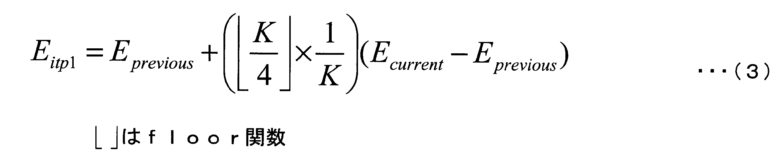
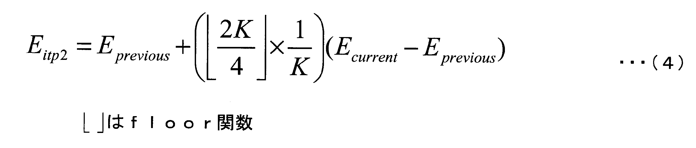
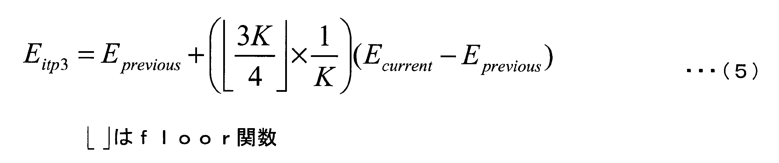
第5の実施形態では、補間処理部が第4の実施形態における補間処理部と異なる構成について説明する。図20は、本実施形態における補償電界信号生成部844の構成を示すブロック図である。補償電界信号生成部844は、第1振幅規格化部8441および補間処理部8442を有する。補間処理部8442は、低域通過フィルタ8443、第1線形補間処理部8444、第2振幅規格化部8445、第2線形補間処理部8446、残留周波数オフセット推定部8447、複素共役演算部8448及び乗算器8449~8452(演算部)を有する。第1振幅規格化部8441、低域通過フィルタ8443、第1線形補間処理部8444、第2振幅規格化部8445及び第2線形補間処理部8446は、図17に示された補償電界信号生成部744中の対応する構成要素と同じ構成である。 (Fifth embodiment)
In the fifth embodiment, a configuration in which an interpolation processing unit is different from the interpolation processing unit in the fourth embodiment will be described. FIG. 20 is a block diagram illustrating a configuration of the compensation electric field
第6の実施形態では、フレーム構造と、残留周波数オフセット推定部とが第5の実施形態と異なる構成について説明する。図22に第6の実施形態における送受信フレームのフレーム構造を示す。なお、図22において、図3に示したものと同じ信号については同一の符号を付している。 (Sixth embodiment)
In the sixth embodiment, a configuration in which the frame structure and the residual frequency offset estimation unit are different from those of the fifth embodiment will be described. FIG. 22 shows a frame structure of a transmission / reception frame in the sixth embodiment. In FIG. 22, the same signals as those shown in FIG. 3 are denoted by the same reference numerals.


第7の実施形態では、同期パターンの複素平面上のマッピングの構成について説明する。
同期パターンとしては、図1における受信装置3が受信デジタル信号における同期パターンを検出する際に相関のピークを検出することができればどのようなパターンを用いてもよい。同期パターンとして用いるパターンの例としては、遅延がゼロになったときのみに相関を有するPRBS(Pseudo Random Bit Sequence;疑似乱数ビット列)を使用することができる。PRBSは遅延がゼロになったときのみに鋭い相関を有する。なお、PRBSはPN系列、M系列と言い換えても同じである。 (Seventh embodiment)
In the seventh embodiment, a configuration of mapping on the complex plane of the synchronization pattern will be described.
As the synchronization pattern, any pattern may be used as long as the receiving
Δθ(n)=(θ(n+1)+ΔθN(n+1))-(θ(n)+ΔθN(n))
=Δθ(n)+(ΔθN(n+1)-ΔθN(n))、
(n=1,2,…,N-1) The phase of the synchronization pattern when the frequency offset occurs is {(θ (1) + ΔθN (1)), (θ (2) + ΔθN (2)),..., (Θ (N) + ΔθN (N))} It can be expressed. The differential detection component Δθ (n) at this time is as follows.
Δθ (n) = (θ (n + 1) + ΔθN (n + 1)) − (θ (n) + ΔθN (n))
= Δθ (n) + (ΔθN (n + 1) −ΔθN (n)),
(N = 1, 2, ..., N-1)
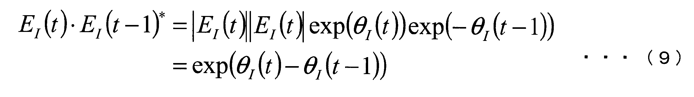
同図に示す構成を用いるメリットとしては、識別部1042Bからパターン同期部1044Bへの出力が1ビットとなるため、パターン同期部1044B及び参照同期パターン記憶部1043Bの回路規模を削減することができる。 In FIG. 28, the I signal component output from the
As an advantage of using the configuration shown in the figure, since the output from the
その他の処理は、第1の実施形態から第6の実施形態と同様に行えばよい。 Once the time position of the synchronization pattern can be detected in the received digital signal, the synchronization pattern repeatedly arrives at the cycle of the symbol length of the transmission / reception frame. Therefore, the synchronization position of each frame is averaged to improve detection sensitivity. be able to.
Other processing may be performed in the same manner as in the first to sixth embodiments.
2…光ファイバ伝送路
3…受信装置
4…デジタル信号処理部
11…信号光源
12…変調信号生成部
13…光変調器
31…局発光源
32…偏波多重光ハイブリッド
33a、33b、33c、33d…バランス検波器
34a、34b、34c、34d…アナログデジタル変換器
41…波長分散補償部
42…適応等化器
43…周波数オフセット補償部
44…位相雑音補償部
45…搬送波位相同期部
46…シンボル識別部
121…パイロットシンボル挿入部
122…同期パターン挿入部
123…シンボルマッピング部
441…パイロットシンボル検出部
442…参照パイロットシンボル記憶部
443…誤差信号演算部
444、644、744、844…補償電界信号生成部
445…位相補償部
1004A、1004B…同期パターン検出部
1041…差動検波部
1042、1042B…識別部
1043、1043B…参照同期パターン記憶部
1044、1044B…パターン同期部
1411、1412…遅延部
1413…複素共役算出部
1414…複素乗算部
4411…参照同期パターン記憶部
4412…同期パターン検出部
4413、4414…パイロットシンボル抽出部
4441、7441、8441…第1振幅規格化部
4442、5442、6442、7442、8442…補間処理部
4443…複素電界内挿部
4444、5443、7443、8443、8510、9510…低域通過フィルタ
4445、7445、8445…第2振幅規格化部
5444、9500…線形補間処理部
6441…位相差演算部
6443、8540、9540…位相電界変換部
6445、8501、8532、9501、9532…遅延器
6446…減算器
6447…位相差算出器
6448、8531、9531…加算器
7444、8444…第1線形補間処理部
7446、8446…第2線形補間処理部
8447、9447…残留周波数オフセット推定部
8448、8502、9502…複素共役演算部
8449、8450、8451、8452、8503、8504、9503、9504…乗算器
8500、9500…スロープ検出部
8520、9520…電界位相変換部
8530、9530…積分部
9550…係数設定部 DESCRIPTION OF
Claims (19)
- 受信した光信号に対するコヒーレント検波により得られる受信複素電界信号に間欠的に挿入された複数のパイロットシンボルを検出するパイロットシンボル検出部と、
前記パイロットシンボル検出部により検出された前記パイロットシンボルと、予め定められた参照シンボルとから、各パイロットシンボルにおける位相変動を示す複素電界誤差信号を算出する誤差信号演算部と、
前記誤差信号演算部が算出した前記複素電界誤差信号に基づき、フィルタ処理を用いて、前記受信複素電界信号における前記パイロットシンボル間の前記位相変動を推定する補償電界信号生成部と、
前記補償電界信号生成部が推定した前記パイロットシンボル間の前記位相変動に基づいて、前記受信複素電界信号に対する位相補償を行う位相雑音補償部と
を備える光伝送システム。 A pilot symbol detector that detects a plurality of pilot symbols intermittently inserted in a received complex electric field signal obtained by coherent detection on a received optical signal;
An error signal calculation unit that calculates a complex electric field error signal indicating a phase variation in each pilot symbol from the pilot symbol detected by the pilot symbol detection unit and a predetermined reference symbol;
Based on the complex electric field error signal calculated by the error signal calculation unit, using a filtering process, a compensation electric field signal generation unit that estimates the phase variation between the pilot symbols in the received complex electric field signal;
An optical transmission system comprising: a phase noise compensation unit that performs phase compensation on the received complex electric field signal based on the phase variation between the pilot symbols estimated by the compensation electric field signal generation unit. - 請求項1に記載の光伝送システムにおいて、
前記補償電界信号生成部は、
前記受信複素電界信号における前記パイロットシンボル間のシンボル区間に対応する長さの信号列を前記複素電界誤差信号間に内挿した信号列を出力する複素電界内挿部と、
前記複素電界内挿部が出力する前記信号列を入力とするローパスフィルタと、
を有する光伝送システム。 The optical transmission system according to claim 1,
The compensation electric field signal generator is
A complex electric field interpolation unit that outputs a signal sequence in which a signal sequence having a length corresponding to a symbol interval between the pilot symbols in the received complex electric field signal is interpolated between the complex electric field error signals;
A low-pass filter that receives the signal sequence output by the complex electric field interpolation unit;
An optical transmission system. - 請求項2に記載の光伝送システムにおいて、
前記複素電界内挿部は、
前記複素電界誤差信号又は振幅がゼロの複素信号の信号列を内挿する
光伝送システム。 The optical transmission system according to claim 2,
The complex electric field interpolation unit is
An optical transmission system for interpolating the complex electric field error signal or a signal sequence of a complex signal having zero amplitude. - 請求項1に記載の光伝送システムにおいて、
前記補償電界信号生成部は、
前記複素電界誤差信号を入力するローパスフィルタと、
前記受信複素電界信号における前記パイロットシンボル間のシンボル区間における位相変動を前記ローパスフィルタの出力の線形補間により算出する線形補間処理部と、
を有する光伝送システム。 The optical transmission system according to claim 1,
The compensation electric field signal generator is
A low-pass filter for inputting the complex electric field error signal;
A linear interpolation processing unit that calculates a phase variation in a symbol interval between the pilot symbols in the received complex electric field signal by linear interpolation of an output of the low-pass filter;
An optical transmission system. - 請求項2から請求項4のいずれか一項に記載の光伝送システムにおいて、
前記補償電界信号生成部は、
前記誤差信号演算部が算出する前記複素電界誤差信号の振幅を規格化する第1振幅規格化部と、
前記位相変動を示す複素信号の振幅を規格化する第2振幅規格化部と、
の内少なくとも前記第2振幅規格化部を更に有する光伝送システム。 In the optical transmission system according to any one of claims 2 to 4,
The compensation electric field signal generator is
A first amplitude normalization unit that normalizes the amplitude of the complex electric field error signal calculated by the error signal calculation unit;
A second amplitude normalization unit that normalizes the amplitude of the complex signal indicating the phase variation;
An optical transmission system further comprising at least the second amplitude normalization unit. - 請求項1に記載の光伝送システムにおいて、
前記補償電界信号生成部は、
前記複素電界誤差信号の位相を示す位相信号を算出する位相差演算部と、
前記受信複素電界信号における前記パイロットシンボル間のシンボル区間に対応する長さの複素電界信号列を、前記位相差演算部が算出した前記位相信号間に挿入した信号列を生成する内挿部と、
前記内挿部が生成する前記信号列を入力するローパスフィルタと、
前記ローパスフィルタの出力を複素信号に変換することにより前記受信複素電界信号における前記パイロットシンボル間の前記シンボル区間の位相変動を算出する位相電界変換部と、
を有する光伝送システム。 The optical transmission system according to claim 1,
The compensation electric field signal generator is
A phase difference calculator that calculates a phase signal indicating the phase of the complex electric field error signal;
An interpolation unit for generating a signal sequence in which a complex electric field signal sequence having a length corresponding to a symbol interval between the pilot symbols in the received complex electric field signal is inserted between the phase signals calculated by the phase difference calculation unit;
A low-pass filter for inputting the signal sequence generated by the interpolation unit;
A phase electric field converter that calculates a phase variation of the symbol interval between the pilot symbols in the received complex electric field signal by converting an output of the low-pass filter into a complex signal;
An optical transmission system. - 請求項6に記載の光伝送システムにおいて、
前記内挿部は、
前記位相信号又はゼロの信号列を内挿する
光伝送システム。 The optical transmission system according to claim 6.
The interpolation part is
An optical transmission system for interpolating the phase signal or zero signal sequence. - 請求項1に記載の光伝送システムにおいて、
前記補償電界信号生成部は、
前記複素電界誤差信号の位相を示す位相信号を算出する位相差演算部と、
前記位相差演算部が算出する前記位相信号を入力するローパスフィルタと、
前記受信複素電界信号における前記パイロットシンボル間のシンボル区間における位相を前記ローパスフィルタの出力に対する線形補間により算出する線形補間処理部と、
前記線形補間処理部が算出する前記位相を複素信号に変換することにより前記受信複素電界信号における前記パイロットシンボル間の前記シンボル区間の位相変動を算出する位相電界変換部と、
を有する光伝送システム。 The optical transmission system according to claim 1,
The compensation electric field signal generator is
A phase difference calculator that calculates a phase signal indicating the phase of the complex electric field error signal;
A low-pass filter for inputting the phase signal calculated by the phase difference calculation unit;
A linear interpolation processing unit that calculates a phase in a symbol interval between the pilot symbols in the received complex electric field signal by linear interpolation with respect to an output of the low-pass filter;
A phase electric field conversion unit for calculating a phase variation of the symbol interval between the pilot symbols in the received complex electric field signal by converting the phase calculated by the linear interpolation processing unit into a complex signal;
An optical transmission system. - 請求項2から請求項8のいずれか一項に記載の光伝送システムにおいて、
前記ローパスフィルタのカットオフ周波数は、
前記パイロットシンボルが位置する間隔に基づいて定められる
光伝送システム。 The optical transmission system according to any one of claims 2 to 8,
The cutoff frequency of the low-pass filter is
An optical transmission system defined based on an interval at which the pilot symbols are located. - 請求項1記載の光伝送システムにおいて、
前記補償電界信号生成部は、
前記複素電界誤差信号を入力するローパスフィルタと、
前記ローパスフィルタの出力のシンボル間隔の区間を、予め定めた個数のシンボル区間に分割し、前記ローパスフィルタの前記出力を除く各分割されたシンボル区間の境界点の位相変動を、前記ローパスフィルタの前記出力から線形補間によって算出する第1線形補間処理部と、
前記ローパスフィルタの前記出力を含む前記境界点の位相変動を示す複素信号の振幅を規格化する振幅規格化部と、
規格化後の前記境界点の位相変動から、前記分割されたシンボル区間内における位相変動を線形補間によって算出する第2線形補間処理部と、
を有する光伝送システム。 The optical transmission system according to claim 1,
The compensation electric field signal generator is
A low-pass filter for inputting the complex electric field error signal;
The interval of the symbol interval of the output of the low-pass filter is divided into a predetermined number of symbol intervals, and the phase variation of the boundary point of each divided symbol interval excluding the output of the low-pass filter is determined by the low-pass filter. A first linear interpolation processing unit that calculates from the output by linear interpolation;
An amplitude normalization unit that normalizes the amplitude of the complex signal indicating the phase fluctuation of the boundary point including the output of the low-pass filter;
A second linear interpolation processing unit that calculates the phase fluctuation in the divided symbol section by linear interpolation from the phase fluctuation of the boundary point after normalization;
An optical transmission system. - 請求項1記載の光伝送システムにおいて、
前記補償電界信号生成部は、
前記複素電界誤差信号を入力する残留周波数オフセット推定部と、
前記複素電界誤差信号を入力する第1のローパスフィルタと、
前記第1のローパスフィルタの入力と出力に前記残留周波数オフセット推定部の出力を乗算する演算部とを備え、
前記残留周波数オフセット推定部は、
前記複素電界誤差信号から残留周波数オフセットの瞬時値を算出する位相スロープ検出部と、
前記位相スロープ検出部の出力値を平均化する第2のローパスフィルタと、
前記第2のローパスフィルタから出力された複素電界値を位相値に変換する電界位相変換部と、
前記電界位相変換部から出力された前記位相値を積分する積分部と、
前記積分部から出力された積分値を位相値として複素電界値に変換する位相電界変換部と
を有する光伝送システム。 The optical transmission system according to claim 1,
The compensation electric field signal generator is
A residual frequency offset estimator for inputting the complex electric field error signal;
A first low-pass filter for inputting the complex electric field error signal;
A calculation unit that multiplies the input and output of the first low-pass filter by the output of the residual frequency offset estimation unit;
The residual frequency offset estimator is
A phase slope detector that calculates an instantaneous value of residual frequency offset from the complex electric field error signal;
A second low-pass filter that averages the output value of the phase slope detector;
An electric field phase converter for converting a complex electric field value output from the second low-pass filter into a phase value;
An integration unit that integrates the phase value output from the electric field phase conversion unit;
An optical transmission system comprising: a phase electric field conversion unit that converts an integrated value output from the integration unit into a complex electric field value as a phase value. - 請求項11記載の光伝送システムにおいて、
前記残留周波数オフセット推定部は、前記パイロットシンボルの間隔に応じて、前記電界位相変換部の出力に係数を乗算する係数設定部を有する光伝送システム。 The optical transmission system according to claim 11.
The residual frequency offset estimation unit is an optical transmission system including a coefficient setting unit that multiplies the output of the electric field phase conversion unit by a coefficient according to the interval of the pilot symbols. - 請求項1に記載の光伝送システムにおいて、
前記パイロットシンボル検出部は、
連続するシンボルからなる同期パターンと、前記同期パターンから予め定められたシンボル数の間隔で送信データに挿入されたパイロットシンボルと、前記送信データとを含む送信フレームを受信して、前記同期パターンの位置を検出する同期パターン検出部と、
検出された前記同期パターンの前記位置から前記パイロットシンボルの位置を検出し、前記パイロットシンボルを抽出するパイロットシンボル抽出部と
を有する光伝送システム。 The optical transmission system according to claim 1,
The pilot symbol detector is
Receiving a transmission frame including a synchronization pattern composed of consecutive symbols, pilot symbols inserted into transmission data at intervals of a predetermined number of symbols from the synchronization pattern, and the position of the synchronization pattern A synchronization pattern detection unit for detecting
An optical transmission system comprising: a pilot symbol extracting unit that detects a position of the pilot symbol from the position of the detected synchronization pattern and extracts the pilot symbol. - 請求項13に記載の光伝送システムにおいて、
前記同期パターンとして疑似乱数ビット列を用いる光伝送システム。 The optical transmission system according to claim 13.
An optical transmission system using a pseudo random number bit string as the synchronization pattern. - 請求項13に記載の光伝送システムにおいて、
前記同期パターンに対する変調において3値以上の振幅レベルが存在する場合、最大の振幅レベル及び最小の振幅レベル以外の振幅レベルのシンボルを前記同期パターンに割り当てる光伝送システム。 The optical transmission system according to claim 13.
An optical transmission system that assigns symbols of amplitude levels other than the maximum amplitude level and the minimum amplitude level to the synchronization pattern when there are three or more amplitude levels in the modulation for the synchronization pattern. - 請求項13に記載の光伝送システムにおいて、前記同期パターンに対する変調において位相が180°異なる2つのシンボルに前記同期パターンを割り当てる光伝送システム。 14. The optical transmission system according to claim 13, wherein the synchronization pattern is assigned to two symbols that are 180 degrees out of phase in modulation with respect to the synchronization pattern.
- 請求項13に記載の光伝送システムにおいて、
前記同期パターン検出部は、前記受信複素電界信号に対して差動検波を行うことにより得られる差動検波信号に対する硬判定結果に基づいて、前記受信複素電界信号に含まれる前記同期パターンを検出する光伝送システム。 The optical transmission system according to claim 13.
The synchronization pattern detection unit detects the synchronization pattern included in the reception complex electric field signal based on a hard decision result for the differential detection signal obtained by performing differential detection on the reception complex electric field signal. Optical transmission system. - 光伝送システムにおける位相補償方法において、
受信した光信号に対するコヒーレント検波により得られる受信複素電界信号に間欠的に挿入された複数のパイロットシンボルを検出するパイロットシンボル検出ステップと、
前記パイロットシンボル検出ステップにおいて検出された前記パイロットシンボルと、予め定められた参照シンボルとから、各パイロットシンボルにおける位相変動を示す複素電界誤差信号を算出する誤差信号演算ステップと、
前記誤差信号演算ステップにおいて算出した前記複素電界誤差信号に基づき、フィルタ処理を用いて、前記受信複素電界信号における前記パイロットシンボル間の前記位相変動を推定する補償電界信号生成ステップと、
前記補償電界信号生成ステップにおいて推定した前記パイロットシンボル間の前記位相変動に基づいて、前記受信複素電界信号に対する位相補償を行う位相雑音補償ステップと、
を有する位相補償方法。 In a phase compensation method in an optical transmission system,
A pilot symbol detecting step for detecting a plurality of pilot symbols intermittently inserted in a received complex electric field signal obtained by coherent detection on a received optical signal;
An error signal calculation step for calculating a complex electric field error signal indicating a phase variation in each pilot symbol from the pilot symbol detected in the pilot symbol detection step and a predetermined reference symbol;
Based on the complex electric field error signal calculated in the error signal calculation step, using a filtering process, a compensation electric field signal generating step for estimating the phase variation between the pilot symbols in the received complex electric field signal;
A phase noise compensation step for performing phase compensation on the received complex electric field signal based on the phase variation between the pilot symbols estimated in the compensation electric field signal generation step;
A phase compensation method comprising: - 受信した光信号に対するコヒーレント検波により得られる受信複素電界信号に間欠的に挿入された複数のパイロットシンボルを検出するパイロットシンボル検出部と、
前記パイロットシンボル検出部により検出された前記パイロットシンボルと、予め定められた参照シンボルとから、各パイロットシンボルにおける位相変動を示す複素電界誤差信号を算出する誤差信号演算部と、
前記誤差信号演算部が算出した前記複素電界誤差信号に基づき、フィルタ処理を用いて、前記受信複素電界信号における前記パイロットシンボル間の前記位相変動を推定する補償電界信号生成部と、
前記補償電界信号生成部が推定した前記パイロットシンボル間の前記位相変動に基づいて、前記受信複素電界信号に対する位相補償を行う位相雑音補償部と、
を備える光受信装置。 A pilot symbol detector that detects a plurality of pilot symbols intermittently inserted in a received complex electric field signal obtained by coherent detection on a received optical signal;
An error signal calculation unit that calculates a complex electric field error signal indicating a phase variation in each pilot symbol from the pilot symbol detected by the pilot symbol detection unit and a predetermined reference symbol;
Based on the complex electric field error signal calculated by the error signal calculation unit, using a filtering process, a compensation electric field signal generation unit that estimates the phase variation between the pilot symbols in the received complex electric field signal;
A phase noise compensation unit that performs phase compensation on the received complex electric field signal based on the phase variation between the pilot symbols estimated by the compensation electric field signal generation unit;
An optical receiver comprising:
Priority Applications (4)
| Application Number | Priority Date | Filing Date | Title |
|---|---|---|---|
| EP14752142.1A EP2942917B1 (en) | 2013-02-13 | 2014-02-13 | Optical transmission system, phase compensation method, and optical reception device |
| US14/766,635 US10038507B2 (en) | 2013-02-13 | 2014-02-13 | Optical transmission system, phase compensation method, and optical reception apparatus |
| CN201480008298.9A CN104969524B (en) | 2013-02-13 | 2014-02-13 | Optical transmission system, phase compensating method and optical receiver apparatus |
| JP2015500275A JP6075902B2 (en) | 2013-02-13 | 2014-02-13 | Optical transmission system, phase compensation method, and optical receiver |
Applications Claiming Priority (2)
| Application Number | Priority Date | Filing Date | Title |
|---|---|---|---|
| JP2013025924 | 2013-02-13 | ||
| JP2013-025924 | 2013-02-13 |
Publications (1)
| Publication Number | Publication Date |
|---|---|
| WO2014126132A1 true WO2014126132A1 (en) | 2014-08-21 |
Family
ID=51354130
Family Applications (1)
| Application Number | Title | Priority Date | Filing Date |
|---|---|---|---|
| PCT/JP2014/053279 WO2014126132A1 (en) | 2013-02-13 | 2014-02-13 | Optical transmission system, phase compensation method, and optical reception device |
Country Status (5)
| Country | Link |
|---|---|
| US (1) | US10038507B2 (en) |
| EP (1) | EP2942917B1 (en) |
| JP (1) | JP6075902B2 (en) |
| CN (1) | CN104969524B (en) |
| WO (1) | WO2014126132A1 (en) |
Cited By (11)
| Publication number | Priority date | Publication date | Assignee | Title |
|---|---|---|---|---|
| JP2015122658A (en) * | 2013-12-24 | 2015-07-02 | 沖電気工業株式会社 | Digital transmitting device, digital receiving device, digital communication system, and synchronization detection method therefor |
| JP6077696B1 (en) * | 2016-03-24 | 2017-02-08 | 日本電信電話株式会社 | Optical transmission system |
| JP2017041666A (en) * | 2015-08-17 | 2017-02-23 | 日本電信電話株式会社 | Phase inversion detection circuit |
| JP6183503B1 (en) * | 2016-06-17 | 2017-08-23 | Nttエレクトロニクス株式会社 | Phase compensation device, phase compensation method, and communication device |
| JP2017158181A (en) * | 2016-02-29 | 2017-09-07 | 富士通株式会社 | Signal transmitter, carrier phase restoration device, and method |
| JP2018042235A (en) * | 2016-09-07 | 2018-03-15 | 富士通株式会社 | Noise intensity detection device, noise intensity detection method, and coherent optical receiver |
| US20190036613A1 (en) * | 2016-06-03 | 2019-01-31 | Ntt Electronics Corporation | Compensation coefficient calculation method |
| JP2019161246A (en) * | 2018-03-07 | 2019-09-19 | 国立大学法人東北大学 | Digital coherent transmission system |
| JP2019198061A (en) * | 2018-05-08 | 2019-11-14 | 富士通株式会社 | Phase noise compensation device and method, receiver |
| WO2021250723A1 (en) * | 2020-06-08 | 2021-12-16 | 日本電信電話株式会社 | Optical reception device and optical reception method |
| CN114070023A (en) * | 2021-11-01 | 2022-02-18 | 许继电源有限公司 | Method and system for synchronizing transmitting side and receiving side of wireless charging and discharging system |
Families Citing this family (30)
| Publication number | Priority date | Publication date | Assignee | Title |
|---|---|---|---|---|
| US10038507B2 (en) * | 2013-02-13 | 2018-07-31 | Nippon Telegraph And Telephone Corporation | Optical transmission system, phase compensation method, and optical reception apparatus |
| EP3793109A1 (en) | 2013-03-13 | 2021-03-17 | Mitsubishi Electric Corporation | Transmission apparatus for suppressing out-of-band interferences |
| JP6458730B2 (en) * | 2013-08-21 | 2019-01-30 | 日本電気株式会社 | Frequency deviation compensation method, frequency deviation compensation method, and program |
| CN105282072B (en) * | 2014-06-30 | 2019-04-30 | 深圳市中兴微电子技术有限公司 | Frequency deviation estimating method and device in optical transport network |
| JP6405833B2 (en) * | 2014-09-25 | 2018-10-17 | 富士通株式会社 | Signal processing apparatus and signal processing method |
| JP2016072696A (en) * | 2014-09-26 | 2016-05-09 | 富士通株式会社 | Distortion compensation device and distortion compensation method |
| US9559786B2 (en) * | 2015-03-17 | 2017-01-31 | Mitsubishi Electric Research Laboratories, Inc. | Pilot-aided coherent receiver for optical communications |
| WO2016161638A1 (en) * | 2015-04-10 | 2016-10-13 | 华为技术有限公司 | Coherent receiver for frequency offset estimation and compensation of coherent light source, method and system |
| CN106161329B (en) * | 2015-04-24 | 2019-07-30 | 富士通株式会社 | Signal processing apparatus, sender unit and receiver |
| US9716603B2 (en) * | 2015-06-08 | 2017-07-25 | Multiphy Ltd. | Framing scheme for continuous optical transmission systems |
| JP2017147622A (en) * | 2016-02-17 | 2017-08-24 | 富士通オプティカルコンポーネンツ株式会社 | Optical transmitter and control method |
| CN107306163B (en) * | 2016-04-22 | 2019-06-28 | 富士通株式会社 | Processing unit, method and the receiver of pilot tone frequency deviation |
| JP6206545B1 (en) * | 2016-06-17 | 2017-10-04 | Nttエレクトロニクス株式会社 | Transmission characteristic compensation apparatus, transmission characteristic compensation method, and communication apparatus |
| CN108023700B (en) * | 2016-11-04 | 2022-08-26 | 中兴通讯股份有限公司 | Pilot frequency parameter feedback and configuration method and device, user terminal and base station |
| US10284303B2 (en) * | 2017-03-17 | 2019-05-07 | Nokia Of America Corporation | Feedforward decision-free pilot-aided phase noise estimation for coherent optical M-QAM systems |
| US10778338B2 (en) * | 2017-04-19 | 2020-09-15 | Mitsubishi Electric Corporation | Optical transmitter, optical receiver, and optical communication system |
| JP2019009647A (en) * | 2017-06-26 | 2019-01-17 | 富士通株式会社 | Transmission device, reception device and estimation method |
| US10476728B2 (en) * | 2017-10-09 | 2019-11-12 | Nec Corporation | Probabilistic shaping for arbitrary modulation formats |
| US10554309B2 (en) * | 2018-01-18 | 2020-02-04 | Mitsubishi Electric Research Laboratories, Inc. | Pilot-aided carrier phase estimation for optical communications |
| JP6627927B1 (en) * | 2018-07-24 | 2020-01-08 | Nttエレクトロニクス株式会社 | Phase fluctuation compensation device, phase fluctuation compensation method, and communication device |
| CN108988954A (en) * | 2018-08-20 | 2018-12-11 | 光梓信息科技(上海)有限公司 | Pulse generation module, optical communication transmitter system and its nonlinear equalization method |
| US10396899B1 (en) * | 2018-08-21 | 2019-08-27 | Fujitsu Limited | Probabilistic constellation shaping using set-partitioned M-QAM |
| EP3672070A1 (en) * | 2018-12-19 | 2020-06-24 | Nxp B.V. | Communications device and method for operating a communications device |
| US10601517B1 (en) * | 2019-01-22 | 2020-03-24 | Fujitsu Limited | Probabilistic shaping on eight-dimensional super-symbols |
| JP7128420B2 (en) * | 2019-02-28 | 2022-08-31 | 日本電信電話株式会社 | Signal processing method, signal processing device and communication system |
| US10903912B2 (en) * | 2019-05-17 | 2021-01-26 | Huawei Technologies Co., Ltd. | Method and apparatus for nonlinear compensation in coherent optical links |
| WO2021240695A1 (en) * | 2020-05-27 | 2021-12-02 | 日本電信電話株式会社 | Optical reception device and clock synchronization method |
| US11394476B2 (en) * | 2020-10-28 | 2022-07-19 | Infinera Corporation | Telecommunication system having a modulation format based upon degradation predictions |
| CN114189410B (en) * | 2021-12-13 | 2024-05-17 | 深圳市日声数码科技有限公司 | Vehicle-mounted digital broadcast audio receiving system |
| CN114337825B (en) * | 2021-12-16 | 2023-06-30 | 成都天奥电子股份有限公司 | Reciprocating variable-frequency optical fiber microwave frequency transmission system and method |
Citations (4)
| Publication number | Priority date | Publication date | Assignee | Title |
|---|---|---|---|---|
| JPH11127208A (en) * | 1997-10-24 | 1999-05-11 | Fujitsu Ltd | Synchronous detection method using pilot symbol and tentative decision data symbol, mobile object communication receiver and interference elimination device |
| JP2002217862A (en) * | 2001-01-19 | 2002-08-02 | Fujitsu General Ltd | Qam-decoding device |
| JP2009141897A (en) * | 2007-12-10 | 2009-06-25 | Nippon Telegr & Teleph Corp <Ntt> | Radio transmission apparatus, radio reception apparatus, radio transmission method, and, radio reception method |
| WO2011140502A1 (en) * | 2010-05-07 | 2011-11-10 | Tyco Electronics Subsea Communications, Llc | Pilot symbol aided carrier phase estimation |
Family Cites Families (31)
| Publication number | Priority date | Publication date | Assignee | Title |
|---|---|---|---|---|
| JPH0371275A (en) * | 1989-08-11 | 1991-03-27 | Hitachi Ltd | Method and device for image transformation |
| JPH118590A (en) * | 1997-04-25 | 1999-01-12 | Oki Electric Ind Co Ltd | Optical transmission system and supervisory and control method therefor |
| JP3022854B1 (en) | 1998-10-23 | 2000-03-21 | 株式会社次世代デジタルテレビジョン放送システム研究所 | Delay profile analyzer and symbol synchronization method |
| US7023928B2 (en) * | 2001-08-06 | 2006-04-04 | Lucent Technologies Inc. | Synchronization of a pilot assisted channel estimation orthogonal frequency division multiplexing system |
| JP4119696B2 (en) * | 2001-08-10 | 2008-07-16 | 松下電器産業株式会社 | Transmitting apparatus, receiving apparatus, and wireless communication method |
| US7548506B2 (en) * | 2001-10-17 | 2009-06-16 | Nortel Networks Limited | System access and synchronization methods for MIMO OFDM communications systems and physical layer packet and preamble design |
| CN1492250A (en) * | 2002-08-16 | 2004-04-28 | �ձ����ŵ绰��ʽ���� | Polarized wave mode chromatic dispersion compensation method and polarized wave mode chromatic dispersion conpensation device |
| US7277517B1 (en) * | 2002-11-15 | 2007-10-02 | 3Com Corporation | Method for achieving symbol alignment to a pre-existing ADSL data exchange |
| CA2470546C (en) * | 2003-06-13 | 2010-08-17 | The Directv Group, Inc. | Method and apparatus for providing carrier synchronization in digital broadcast and interactive systems |
| JP4287777B2 (en) | 2003-09-26 | 2009-07-01 | 日本放送協会 | Transmitting apparatus and receiving apparatus |
| US7539255B2 (en) * | 2004-06-23 | 2009-05-26 | Texas Insturments Incorporated | Using multiple pilot signals for timing error estimation in digital subscriber line communications |
| KR100668663B1 (en) * | 2005-09-30 | 2007-01-12 | 한국전자통신연구원 | Apparatus and method for automatic gain control of mobile station in ofdm system |
| WO2007094608A1 (en) * | 2006-02-14 | 2007-08-23 | Samsung Electronics Co., Ltd. | Channel estimation method and apparatus using linear interpolation scheme in orthogonal frequency division multiplexing system and receiver using the same |
| US7822069B2 (en) * | 2006-05-22 | 2010-10-26 | Qualcomm Incorporated | Phase correction for OFDM and MIMO transmissions |
| JP2008177807A (en) * | 2007-01-18 | 2008-07-31 | Fujitsu Ltd | Transmission line characteristic estimation apparatus, receiver and transmission line characteristic estimation method |
| TWI365650B (en) * | 2008-04-09 | 2012-06-01 | Ind Tech Res Inst | Transmission method of wireless signal and transmitter using the same |
| JP2009302793A (en) * | 2008-06-12 | 2009-12-24 | Mitsubishi Electric Corp | Carrier frequency error detector |
| JP5136236B2 (en) * | 2008-06-19 | 2013-02-06 | 富士通株式会社 | Optical receiver |
| JP4567088B2 (en) * | 2008-09-01 | 2010-10-20 | 三菱電機株式会社 | OFDM signal receiving apparatus and receiving method |
| US8218979B2 (en) * | 2009-06-30 | 2012-07-10 | Alcatel Lucent | System, method and apparatus for coherent optical OFDM |
| WO2011007803A1 (en) * | 2009-07-17 | 2011-01-20 | 日本電信電話株式会社 | Wavelength dispersion amount calculation device, optical signal reception device, optical signal transmission device, and wavelength dispersion amount calculation method |
| US8428537B2 (en) * | 2010-05-26 | 2013-04-23 | Intel Mobile Communications GmbH | Receiver having adjustable channel estimation bandwidth |
| US8971424B2 (en) * | 2010-05-31 | 2015-03-03 | Ceragon Networks Ltd. | Combining pilot-symbol-based phase estimation with data-symbol-based phase estimation |
| US8750441B2 (en) * | 2010-12-20 | 2014-06-10 | Texas Instruments Incorporated | Signal cancellation to reduce phase noise, period jitter, and other contamination in local oscillator, frequency timing, or other timing generators or signal sources |
| WO2012142760A1 (en) * | 2011-04-21 | 2012-10-26 | Huawei Technologies Co., Ltd. | Phase error compensation arrangement and phase error compensation method |
| US8879922B2 (en) * | 2011-10-11 | 2014-11-04 | Alcatel Lucent | System, method and apparatus for high-sensitivity optical detection |
| JP5886984B2 (en) * | 2013-01-25 | 2016-03-16 | 日本電信電話株式会社 | Optical receiver and phase cycle slip reduction method |
| JP6126404B2 (en) | 2013-02-13 | 2017-05-10 | 日本電信電話株式会社 | Transmission / reception system and communication method |
| US10038507B2 (en) * | 2013-02-13 | 2018-07-31 | Nippon Telegraph And Telephone Corporation | Optical transmission system, phase compensation method, and optical reception apparatus |
| US9544061B2 (en) * | 2015-03-04 | 2017-01-10 | Alcatel-Lucent Usa Inc. | Switched optical receiver |
| US9667458B1 (en) * | 2015-06-03 | 2017-05-30 | Qualcomm Incorporated | Feed-forward phase tracking |
-
2014
- 2014-02-13 US US14/766,635 patent/US10038507B2/en active Active
- 2014-02-13 CN CN201480008298.9A patent/CN104969524B/en active Active
- 2014-02-13 EP EP14752142.1A patent/EP2942917B1/en active Active
- 2014-02-13 JP JP2015500275A patent/JP6075902B2/en active Active
- 2014-02-13 WO PCT/JP2014/053279 patent/WO2014126132A1/en active Application Filing
Patent Citations (4)
| Publication number | Priority date | Publication date | Assignee | Title |
|---|---|---|---|---|
| JPH11127208A (en) * | 1997-10-24 | 1999-05-11 | Fujitsu Ltd | Synchronous detection method using pilot symbol and tentative decision data symbol, mobile object communication receiver and interference elimination device |
| JP2002217862A (en) * | 2001-01-19 | 2002-08-02 | Fujitsu General Ltd | Qam-decoding device |
| JP2009141897A (en) * | 2007-12-10 | 2009-06-25 | Nippon Telegr & Teleph Corp <Ntt> | Radio transmission apparatus, radio reception apparatus, radio transmission method, and, radio reception method |
| WO2011140502A1 (en) * | 2010-05-07 | 2011-11-10 | Tyco Electronics Subsea Communications, Llc | Pilot symbol aided carrier phase estimation |
Non-Patent Citations (3)
| Title |
|---|
| A. J. VITERBI ET AL.: "Nonlinear Estimation of PSK-Modulated Carrier Phase with Application to Burst Digital Transmission", IEEE TRANSACTIONS ON INFORMATION THEORY, vol. IT-29, no. 4, July 1983 (1983-07-01), XP000760812, DOI: doi:10.1109/TIT.1983.1056713 |
| T. NAKAGAWA ET AL., NON-DATA-AIDED WIDE-RANGE FREQUENCY OFFSET ESTIMATOR FOR QAM OPTICAL COHERENT RECEIVERS |
| T. NAKAGAWA ET AL.: "Non-data-aided wide-range frequency offset estimator for QAM optical coherent receivers", 2011 OPTICAL FIBER COMMUNICATION CONFERENCE AND EXPOSITION (OFC/ NFOEC) AND THE NATIONAL FIBER OPTIC ENGINEERS CONFERENCE, 2011, pages 1 - 3, XP031946233 * |
Cited By (19)
| Publication number | Priority date | Publication date | Assignee | Title |
|---|---|---|---|---|
| JP2015122658A (en) * | 2013-12-24 | 2015-07-02 | 沖電気工業株式会社 | Digital transmitting device, digital receiving device, digital communication system, and synchronization detection method therefor |
| JP2017041666A (en) * | 2015-08-17 | 2017-02-23 | 日本電信電話株式会社 | Phase inversion detection circuit |
| JP7091025B2 (en) | 2016-02-29 | 2022-06-27 | 富士通株式会社 | Signal transmitter, carrier phase restorer and method |
| JP2017158181A (en) * | 2016-02-29 | 2017-09-07 | 富士通株式会社 | Signal transmitter, carrier phase restoration device, and method |
| JP6077696B1 (en) * | 2016-03-24 | 2017-02-08 | 日本電信電話株式会社 | Optical transmission system |
| JP2017175441A (en) * | 2016-03-24 | 2017-09-28 | 日本電信電話株式会社 | Optical transmission system |
| US20190036613A1 (en) * | 2016-06-03 | 2019-01-31 | Ntt Electronics Corporation | Compensation coefficient calculation method |
| US10396895B2 (en) * | 2016-06-03 | 2019-08-27 | Ntt Electronics Corporation | Compensation coefficient calculation method |
| JP6183503B1 (en) * | 2016-06-17 | 2017-08-23 | Nttエレクトロニクス株式会社 | Phase compensation device, phase compensation method, and communication device |
| JP2017225075A (en) * | 2016-06-17 | 2017-12-21 | Nttエレクトロニクス株式会社 | Phase compensation device, phase compensation method, and communication device |
| WO2017217100A1 (en) * | 2016-06-17 | 2017-12-21 | Nttエレクトロニクス株式会社 | Phase compensation device, phase compensation method and communication apparatus |
| JP2018042235A (en) * | 2016-09-07 | 2018-03-15 | 富士通株式会社 | Noise intensity detection device, noise intensity detection method, and coherent optical receiver |
| JP7038408B2 (en) | 2018-03-07 | 2022-03-18 | 国立大学法人東北大学 | Digital coherent transmission system |
| JP2019161246A (en) * | 2018-03-07 | 2019-09-19 | 国立大学法人東北大学 | Digital coherent transmission system |
| JP2019198061A (en) * | 2018-05-08 | 2019-11-14 | 富士通株式会社 | Phase noise compensation device and method, receiver |
| JP7225902B2 (en) | 2018-05-08 | 2023-02-21 | 富士通株式会社 | PHASE NOISE COMPENSATION APPARATUS AND METHOD, RECEIVER |
| WO2021250723A1 (en) * | 2020-06-08 | 2021-12-16 | 日本電信電話株式会社 | Optical reception device and optical reception method |
| JP7307391B2 (en) | 2020-06-08 | 2023-07-12 | 日本電信電話株式会社 | Optical receiving device and optical receiving method |
| CN114070023A (en) * | 2021-11-01 | 2022-02-18 | 许继电源有限公司 | Method and system for synchronizing transmitting side and receiving side of wireless charging and discharging system |
Also Published As
| Publication number | Publication date |
|---|---|
| US20150372766A1 (en) | 2015-12-24 |
| JP6075902B2 (en) | 2017-02-08 |
| US10038507B2 (en) | 2018-07-31 |
| CN104969524B (en) | 2018-11-30 |
| EP2942917A1 (en) | 2015-11-11 |
| EP2942917B1 (en) | 2018-05-23 |
| EP2942917A4 (en) | 2017-02-15 |
| JPWO2014126132A1 (en) | 2017-02-02 |
| CN104969524A (en) | 2015-10-07 |
Similar Documents
| Publication | Publication Date | Title |
|---|---|---|
| JP6075902B2 (en) | Optical transmission system, phase compensation method, and optical receiver | |
| JP5163454B2 (en) | Frequency offset detection apparatus and detection method used in digital coherent optical receiver | |
| JP5651990B2 (en) | Digital coherent receiver and receiving method | |
| JP5886984B2 (en) | Optical receiver and phase cycle slip reduction method | |
| JP5406989B2 (en) | Optical receiver and optical transmission system | |
| EP1962443B1 (en) | Digital phase estimator, digital phase locked loop and optical coherent receiver | |
| JP5590090B2 (en) | Frequency offset compensation apparatus and method, and optical coherent receiver | |
| US8873968B2 (en) | Optical field receiver, optical multilevel signal receiver, and optical transmission system | |
| JP4893672B2 (en) | Coherent optical communication apparatus and method | |
| JP5136236B2 (en) | Optical receiver | |
| JP2009130935A (en) | Optical coherent receiver, frequency offset estimating apparatus and method for optical coherent receiver | |
| CN102725960A (en) | Method for phase and oscillator frequency estimation | |
| WO2020174656A1 (en) | Reception signal processing device, reception signal processing method, and optical receiver | |
| JPWO2019171587A1 (en) | Optical receiver and optical transceiver system | |
| WO2021240695A1 (en) | Optical reception device and clock synchronization method | |
| JP2014045426A (en) | Clock timing recovery device, clock timing recovery method and digital coherent receiver | |
| US9276674B2 (en) | Estimating phase using test phases and interpolation for modulation formats using multiple sub-carriers | |
| WO2022176005A1 (en) | Optical reception device and frequency offset compensation method | |
| EP2976852B1 (en) | Timing recovery apparatus | |
| EP3866425B1 (en) | Reception device, reception method, and program | |
| US20240178921A1 (en) | Optical receiving apparatus and frequency offset compensation method | |
| Bäuerle et al. | Blind real-time multi-format carrier recovery for flexible optical networks | |
| de Arruda Mello et al. | Carrier Recovery | |
| EP3089383A1 (en) | Method and apparatus for estimating phase of phase-modulated optical signals |
Legal Events
| Date | Code | Title | Description |
|---|---|---|---|
| 121 | Ep: the epo has been informed by wipo that ep was designated in this application |
Ref document number: 14752142 Country of ref document: EP Kind code of ref document: A1 |
|
| ENP | Entry into the national phase |
Ref document number: 2015500275 Country of ref document: JP Kind code of ref document: A |
|
| WWE | Wipo information: entry into national phase |
Ref document number: 2014752142 Country of ref document: EP |
|
| WWE | Wipo information: entry into national phase |
Ref document number: 14766635 Country of ref document: US |
|
| NENP | Non-entry into the national phase |
Ref country code: DE |