WO2014061274A1 - Image sensor and image sensor device - Google Patents
Image sensor and image sensor device Download PDFInfo
- Publication number
- WO2014061274A1 WO2014061274A1 PCT/JP2013/006171 JP2013006171W WO2014061274A1 WO 2014061274 A1 WO2014061274 A1 WO 2014061274A1 JP 2013006171 W JP2013006171 W JP 2013006171W WO 2014061274 A1 WO2014061274 A1 WO 2014061274A1
- Authority
- WO
- WIPO (PCT)
- Prior art keywords
- light
- image sensor
- scanning direction
- main scanning
- read
- Prior art date
Links
- 238000005286 illumination Methods 0.000 claims abstract description 26
- 230000003287 optical effect Effects 0.000 claims description 52
- 238000006243 chemical reaction Methods 0.000 claims description 47
- 238000003384 imaging method Methods 0.000 claims description 9
- 238000000411 transmission spectrum Methods 0.000 claims description 7
- OAICVXFJPJFONN-UHFFFAOYSA-N Phosphorus Chemical compound [P] OAICVXFJPJFONN-UHFFFAOYSA-N 0.000 claims description 2
- 230000005284 excitation Effects 0.000 claims description 2
- 230000001678 irradiating effect Effects 0.000 claims description 2
- 238000000149 argon plasma sintering Methods 0.000 description 31
- 230000005540 biological transmission Effects 0.000 description 21
- 238000010586 diagram Methods 0.000 description 18
- 238000001514 detection method Methods 0.000 description 10
- 230000003595 spectral effect Effects 0.000 description 8
- 238000001228 spectrum Methods 0.000 description 6
- 239000003086 colorant Substances 0.000 description 5
- 230000035945 sensitivity Effects 0.000 description 5
- 239000011521 glass Substances 0.000 description 4
- 238000003491 array Methods 0.000 description 3
- 230000004907 flux Effects 0.000 description 3
- 230000037303 wrinkles Effects 0.000 description 3
- 230000000694 effects Effects 0.000 description 2
- 239000005357 flat glass Substances 0.000 description 2
- 230000002093 peripheral effect Effects 0.000 description 2
- 230000005855 radiation Effects 0.000 description 2
- 230000001360 synchronised effect Effects 0.000 description 2
- 230000006866 deterioration Effects 0.000 description 1
- 238000000295 emission spectrum Methods 0.000 description 1
- 238000004519 manufacturing process Methods 0.000 description 1
- 239000000463 material Substances 0.000 description 1
- 239000002184 metal Substances 0.000 description 1
- 238000000034 method Methods 0.000 description 1
- 239000011347 resin Substances 0.000 description 1
- 229920005989 resin Polymers 0.000 description 1
- 238000011144 upstream manufacturing Methods 0.000 description 1
Images


Classifications
-
- H—ELECTRICITY
- H01—ELECTRIC ELEMENTS
- H01L—SEMICONDUCTOR DEVICES NOT COVERED BY CLASS H10
- H01L27/00—Devices consisting of a plurality of semiconductor or other solid-state components formed in or on a common substrate
- H01L27/14—Devices consisting of a plurality of semiconductor or other solid-state components formed in or on a common substrate including semiconductor components sensitive to infrared radiation, light, electromagnetic radiation of shorter wavelength or corpuscular radiation and specially adapted either for the conversion of the energy of such radiation into electrical energy or for the control of electrical energy by such radiation
- H01L27/144—Devices controlled by radiation
- H01L27/146—Imager structures
- H01L27/14601—Structural or functional details thereof
- H01L27/14625—Optical elements or arrangements associated with the device
- H01L27/14629—Reflectors
-
- G—PHYSICS
- G01—MEASURING; TESTING
- G01J—MEASUREMENT OF INTENSITY, VELOCITY, SPECTRAL CONTENT, POLARISATION, PHASE OR PULSE CHARACTERISTICS OF INFRARED, VISIBLE OR ULTRAVIOLET LIGHT; COLORIMETRY; RADIATION PYROMETRY
- G01J1/00—Photometry, e.g. photographic exposure meter
- G01J1/42—Photometry, e.g. photographic exposure meter using electric radiation detectors
-
- G—PHYSICS
- G03—PHOTOGRAPHY; CINEMATOGRAPHY; ANALOGOUS TECHNIQUES USING WAVES OTHER THAN OPTICAL WAVES; ELECTROGRAPHY; HOLOGRAPHY
- G03B—APPARATUS OR ARRANGEMENTS FOR TAKING PHOTOGRAPHS OR FOR PROJECTING OR VIEWING THEM; APPARATUS OR ARRANGEMENTS EMPLOYING ANALOGOUS TECHNIQUES USING WAVES OTHER THAN OPTICAL WAVES; ACCESSORIES THEREFOR
- G03B27/00—Photographic printing apparatus
- G03B27/32—Projection printing apparatus, e.g. enlarger, copying camera
- G03B27/52—Details
- G03B27/54—Lamp housings; Illuminating means
-
- G—PHYSICS
- G07—CHECKING-DEVICES
- G07D—HANDLING OF COINS OR VALUABLE PAPERS, e.g. TESTING, SORTING BY DENOMINATIONS, COUNTING, DISPENSING, CHANGING OR DEPOSITING
- G07D7/00—Testing specially adapted to determine the identity or genuineness of valuable papers or for segregating those which are unacceptable, e.g. banknotes that are alien to a currency
- G07D7/06—Testing specially adapted to determine the identity or genuineness of valuable papers or for segregating those which are unacceptable, e.g. banknotes that are alien to a currency using wave or particle radiation
- G07D7/12—Visible light, infrared or ultraviolet radiation
- G07D7/121—Apparatus characterised by sensor details
-
- H—ELECTRICITY
- H04—ELECTRIC COMMUNICATION TECHNIQUE
- H04N—PICTORIAL COMMUNICATION, e.g. TELEVISION
- H04N1/00—Scanning, transmission or reproduction of documents or the like, e.g. facsimile transmission; Details thereof
- H04N1/024—Details of scanning heads ; Means for illuminating the original
- H04N1/028—Details of scanning heads ; Means for illuminating the original for picture information pick-up
- H04N1/02815—Means for illuminating the original, not specific to a particular type of pick-up head
- H04N1/0282—Using a single or a few point light sources, e.g. a laser diode
- H04N1/02835—Using a single or a few point light sources, e.g. a laser diode in combination with a light guide, e.g. optical fibre, glass plate
-
- H—ELECTRICITY
- H04—ELECTRIC COMMUNICATION TECHNIQUE
- H04N—PICTORIAL COMMUNICATION, e.g. TELEVISION
- H04N1/00—Scanning, transmission or reproduction of documents or the like, e.g. facsimile transmission; Details thereof
- H04N1/024—Details of scanning heads ; Means for illuminating the original
- H04N1/028—Details of scanning heads ; Means for illuminating the original for picture information pick-up
- H04N1/03—Details of scanning heads ; Means for illuminating the original for picture information pick-up with photodetectors arranged in a substantially linear array
- H04N1/031—Details of scanning heads ; Means for illuminating the original for picture information pick-up with photodetectors arranged in a substantially linear array the photodetectors having a one-to-one and optically positive correspondence with the scanned picture elements, e.g. linear contact sensors
- H04N1/0318—Integral pick-up heads, i.e. self-contained heads whose basic elements are a light-source, a lens array and a photodetector array which are supported by a single-piece frame
-
- H—ELECTRICITY
- H04—ELECTRIC COMMUNICATION TECHNIQUE
- H04N—PICTORIAL COMMUNICATION, e.g. TELEVISION
- H04N1/00—Scanning, transmission or reproduction of documents or the like, e.g. facsimile transmission; Details thereof
- H04N1/04—Scanning arrangements, i.e. arrangements for the displacement of active reading or reproducing elements relative to the original or reproducing medium, or vice versa
- H04N1/12—Scanning arrangements, i.e. arrangements for the displacement of active reading or reproducing elements relative to the original or reproducing medium, or vice versa using the sheet-feed movement or the medium-advance or the drum-rotation movement as the slow scanning component, e.g. arrangements for the main-scanning
- H04N1/121—Feeding arrangements
- H04N1/1215—Feeding using one or more cylindrical platens or rollers in the immediate vicinity of the main scanning line
-
- H—ELECTRICITY
- H04—ELECTRIC COMMUNICATION TECHNIQUE
- H04N—PICTORIAL COMMUNICATION, e.g. TELEVISION
- H04N1/00—Scanning, transmission or reproduction of documents or the like, e.g. facsimile transmission; Details thereof
- H04N1/04—Scanning arrangements, i.e. arrangements for the displacement of active reading or reproducing elements relative to the original or reproducing medium, or vice versa
- H04N1/203—Simultaneous scanning of two or more separate pictures, e.g. two sides of the same sheet
- H04N1/2032—Simultaneous scanning of two or more separate pictures, e.g. two sides of the same sheet of two pictures corresponding to two sides of a single medium
- H04N1/2034—Simultaneous scanning of two or more separate pictures, e.g. two sides of the same sheet of two pictures corresponding to two sides of a single medium at identical corresponding positions, i.e. without time delay between the two image signals
-
- H—ELECTRICITY
- H04—ELECTRIC COMMUNICATION TECHNIQUE
- H04N—PICTORIAL COMMUNICATION, e.g. TELEVISION
- H04N2201/00—Indexing scheme relating to scanning, transmission or reproduction of documents or the like, and to details thereof
- H04N2201/024—Indexing scheme relating to scanning, transmission or reproduction of documents or the like, and to details thereof deleted
- H04N2201/028—Indexing scheme relating to scanning, transmission or reproduction of documents or the like, and to details thereof deleted for picture information pick-up
- H04N2201/03—Indexing scheme relating to scanning, transmission or reproduction of documents or the like, and to details thereof deleted for picture information pick-up deleted
- H04N2201/031—Indexing scheme relating to scanning, transmission or reproduction of documents or the like, and to details thereof deleted for picture information pick-up deleted deleted
- H04N2201/03104—Integral pick-up heads, i.e. self-contained heads whose basic elements are a light source, a lens and a photodetector supported by a single-piece frame
- H04N2201/03108—Components of integral heads
- H04N2201/03112—Light source
-
- H—ELECTRICITY
- H04—ELECTRIC COMMUNICATION TECHNIQUE
- H04N—PICTORIAL COMMUNICATION, e.g. TELEVISION
- H04N2201/00—Indexing scheme relating to scanning, transmission or reproduction of documents or the like, and to details thereof
- H04N2201/024—Indexing scheme relating to scanning, transmission or reproduction of documents or the like, and to details thereof deleted
- H04N2201/028—Indexing scheme relating to scanning, transmission or reproduction of documents or the like, and to details thereof deleted for picture information pick-up
- H04N2201/03—Indexing scheme relating to scanning, transmission or reproduction of documents or the like, and to details thereof deleted for picture information pick-up deleted
- H04N2201/031—Indexing scheme relating to scanning, transmission or reproduction of documents or the like, and to details thereof deleted for picture information pick-up deleted deleted
- H04N2201/03104—Integral pick-up heads, i.e. self-contained heads whose basic elements are a light source, a lens and a photodetector supported by a single-piece frame
- H04N2201/03108—Components of integral heads
- H04N2201/0312—Reflecting element upstream of the scanned picture elements
-
- H—ELECTRICITY
- H04—ELECTRIC COMMUNICATION TECHNIQUE
- H04N—PICTORIAL COMMUNICATION, e.g. TELEVISION
- H04N2201/00—Indexing scheme relating to scanning, transmission or reproduction of documents or the like, and to details thereof
- H04N2201/024—Indexing scheme relating to scanning, transmission or reproduction of documents or the like, and to details thereof deleted
- H04N2201/028—Indexing scheme relating to scanning, transmission or reproduction of documents or the like, and to details thereof deleted for picture information pick-up
- H04N2201/03—Indexing scheme relating to scanning, transmission or reproduction of documents or the like, and to details thereof deleted for picture information pick-up deleted
- H04N2201/031—Indexing scheme relating to scanning, transmission or reproduction of documents or the like, and to details thereof deleted for picture information pick-up deleted deleted
- H04N2201/03104—Integral pick-up heads, i.e. self-contained heads whose basic elements are a light source, a lens and a photodetector supported by a single-piece frame
- H04N2201/03108—Components of integral heads
- H04N2201/03125—Light guide upstream of the scanned picture elements
-
- H—ELECTRICITY
- H04—ELECTRIC COMMUNICATION TECHNIQUE
- H04N—PICTORIAL COMMUNICATION, e.g. TELEVISION
- H04N2201/00—Indexing scheme relating to scanning, transmission or reproduction of documents or the like, and to details thereof
- H04N2201/024—Indexing scheme relating to scanning, transmission or reproduction of documents or the like, and to details thereof deleted
- H04N2201/028—Indexing scheme relating to scanning, transmission or reproduction of documents or the like, and to details thereof deleted for picture information pick-up
- H04N2201/03—Indexing scheme relating to scanning, transmission or reproduction of documents or the like, and to details thereof deleted for picture information pick-up deleted
- H04N2201/031—Indexing scheme relating to scanning, transmission or reproduction of documents or the like, and to details thereof deleted for picture information pick-up deleted deleted
- H04N2201/03104—Integral pick-up heads, i.e. self-contained heads whose basic elements are a light source, a lens and a photodetector supported by a single-piece frame
- H04N2201/03108—Components of integral heads
- H04N2201/03133—Window, i.e. a transparent member mounted in the frame
-
- H—ELECTRICITY
- H04—ELECTRIC COMMUNICATION TECHNIQUE
- H04N—PICTORIAL COMMUNICATION, e.g. TELEVISION
- H04N2201/00—Indexing scheme relating to scanning, transmission or reproduction of documents or the like, and to details thereof
- H04N2201/024—Indexing scheme relating to scanning, transmission or reproduction of documents or the like, and to details thereof deleted
- H04N2201/028—Indexing scheme relating to scanning, transmission or reproduction of documents or the like, and to details thereof deleted for picture information pick-up
- H04N2201/03—Indexing scheme relating to scanning, transmission or reproduction of documents or the like, and to details thereof deleted for picture information pick-up deleted
- H04N2201/031—Indexing scheme relating to scanning, transmission or reproduction of documents or the like, and to details thereof deleted for picture information pick-up deleted deleted
- H04N2201/03104—Integral pick-up heads, i.e. self-contained heads whose basic elements are a light source, a lens and a photodetector supported by a single-piece frame
- H04N2201/03108—Components of integral heads
- H04N2201/03141—Photodetector lens
-
- H—ELECTRICITY
- H04—ELECTRIC COMMUNICATION TECHNIQUE
- H04N—PICTORIAL COMMUNICATION, e.g. TELEVISION
- H04N2201/00—Indexing scheme relating to scanning, transmission or reproduction of documents or the like, and to details thereof
- H04N2201/024—Indexing scheme relating to scanning, transmission or reproduction of documents or the like, and to details thereof deleted
- H04N2201/028—Indexing scheme relating to scanning, transmission or reproduction of documents or the like, and to details thereof deleted for picture information pick-up
- H04N2201/03—Indexing scheme relating to scanning, transmission or reproduction of documents or the like, and to details thereof deleted for picture information pick-up deleted
- H04N2201/031—Indexing scheme relating to scanning, transmission or reproduction of documents or the like, and to details thereof deleted for picture information pick-up deleted deleted
- H04N2201/03104—Integral pick-up heads, i.e. self-contained heads whose basic elements are a light source, a lens and a photodetector supported by a single-piece frame
- H04N2201/03108—Components of integral heads
- H04N2201/03145—Photodetector
Definitions
- the present invention relates to an image sensor and an image sensor device that read an image of a reading target (object to be read) having a portion that reflects light and a portion that transmits light.
- a paper sheet such as a banknote, which is a read object having a portion that reflects light and a portion that transmits light, securities, and the like are read using an optical sensor.
- a paper sheet reading apparatus using an optical sensor performs a reading process by the following operation. First, a plurality of lights having different wavelengths are irradiated onto a paper sheet. Next, the optical information of the paper sheet is detected by reading the reflected light information and the transmitted light information from the reflected light of the irradiated light reflected on the paper sheet. The detected optical information is used to determine the authenticity of paper sheets and the degree of distribution deterioration.
- the optical detection unit that provides such optical information to the reader includes an illumination system that illuminates the paper sheet, an imaging system that forms an image of reflected or transmitted light from the paper sheet, and an electrical signal that indicates the optical information formed. It is composed of photoelectric conversion elements that convert to In recent years, the amount of detection information required for an optical detection unit has been dramatically increased against the background of an increase in demand for banknote discrimination.
- the detection specification is determined by the single-sided information and double-sided information of the object to be read, or the combination of reflected light information and transmitted light information.
- the detection specification is determined by the single-sided information and double-sided information of the object to be read, or the combination of reflected light information and transmitted light information.
- Patent Document 1 discloses an object in which an image sensor including an illumination system, an imaging system, a photoelectric conversion element, and the like for reading reflected light information is arranged on one surface side of an object to be read. ing.
- an image sensor including an illumination system, an imaging system, a photoelectric conversion element, and the like for reading reflected light information is arranged on one surface side of an object to be read.
- irradiation light that coincides with the imaging optical axis of the image sensor (that is, the image sensor disposed on the one surface side of the object to be read)
- a dedicated lighting unit having an axis is arranged.
- the image sensor obtains reflected light information by illuminating the object to be read by its own illumination system and forming an image of the reflected light from the object to be read on the photoelectric conversion element.
- the image sensor transmits light when the dedicated illumination unit illuminates the read object through the read object and the scattered light reaches the photoelectric conversion element via the imaging lens of the image sensor.
- An example devised to obtain optical information is shown.
- a dedicated illumination system corresponding to each is provided, while an imaging system and a photoelectric conversion element are shared. With this configuration, an optical detector having a good space factor and high versatility can be obtained.
- the object of the present invention is to solve the above problems. That is, the reflected light information on both sides of the object to be read and the transmitted light information from both sides of the object to be read are obtained.
- the object is to obtain a sensor device.
- An illumination unit extending in the main scanning direction for irradiating the object to be read, a rod lens array for forming an image of light from the object to be read, and converting the light imaged by the rod lens array into an electrical signal
- a light receiving unit that illuminates the first irradiation region of the object to be read, and the illumination unit is separated from the normal light direction of the object to be read and from the first irradiation region in the sub-scanning direction. Inclined light that is inclined by a predetermined angle from the normal direction of the reading object that irradiates the second irradiation region is irradiated.
- a sensor device can be obtained.
- FIG. 5 is a side sectional view of illumination means according to Embodiments 1 to 4 of the present invention. It is a flexible printed circuit board figure concerning Embodiment 1 and 4 of this invention. It is sectional drawing of the light guide which concerns on Embodiment 1 and 4 of this invention.
- 1 is an overall block diagram according to Embodiment 1 of the present invention. It is a timing diagram of the image sensor which concerns on Embodiment 1 of this invention. It is a timing diagram of the image sensor which concerns on Embodiment 1 of this invention. It is an optical path figure to the transversal direction of the light guide without a cut concerning Embodiment 2 of the present invention.
- It is a figure of the photoelectric conversion element array which consists of 3 rows with the spectral transmission spectrum filter which concerns on Embodiment 4 of this invention.
- the reading target (read object) of the image sensor and the image sensor device is a paper sheet such as a banknote, a securities, a check
- a check will be described as an example.
- the present invention can be implemented if the object has a part that reflects light and a part that transmits light.
- the same reference numerals denote the same or corresponding parts, and detailed descriptions thereof are omitted.
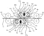
- FIG. 1 is a cross-sectional view of the image sensor device according to the first embodiment.
- reference numeral 17 denotes a paper sheet such as a bill, a security, or a check to be read outside the image sensor device, which has reflected light information and transmitted light information such as a watermark. .
- two image sensors 91a and 91b having the same outer shape and the same structure rotate 180 degrees around the main scanning direction so that the paper sheet 17 is sandwiched from above and below, And each top plate glass 1a and 1b is arrange
- the paper sheet 17 is moved in the left-right direction (see FIG. 1) by a conveyance system using the rollers 20 installed on the upstream side and the downstream side in the conveyance direction through the gap formed by the two top glass plates 1a and 1b. It can be conveyed in the sub-scanning direction). Reading the image on the paper sheet 17 is realized by simultaneously driving and scanning the upper and lower image sensors 91a and 91b while conveying the paper sheet 17 at a constant speed.
- the two image sensors 91a and 91b shown in FIG. 1 have the same external shape and the same structure with respect to the basic configuration. Accordingly, the structure of the lower image sensor 91a in FIG. 1 will be mainly described (hereinafter, the reference numerals in parentheses indicate components of the upper image sensor 91b).
- 1a (1b) is a top plate glass
- 2a (2b) and 3a (3b) are light guides having a circular cross section that illuminates the paper sheet 17 through the glass plate 1a (1b)
- 21a ( 21b), 22a (22b) and 23a (23b) are light scattering devices that reflect and scatter light provided over a part of the outer peripheral surface of the light guides 2a (2b) and 3a (3b) and substantially over the reading width.
- 5a (5b) is a rod lens array for imaging reflected light and transmitted light from the paper sheet 17
- 6a (6b) is a one-dimensional photoelectric conversion element array for converting the imaged light information into an electrical signal
- 7a (7b) is a printed circuit board on which the one-dimensional photoelectric conversion element array is mounted
- 51a (51b) is a signal processing unit mounted on the printed circuit board 7a (7b)
- 8a (8b) is a housing for holding these members.
- FIG. 2 shows a side sectional view of the illumination means according to the first embodiment.
- 9a (9b) and 11a (11b) are flexible printed boards on which light sources (LEDs) are mounted
- 10a (10b) and 12a (12b) are light guides 2a (2b) and 3a (3b), respectively. It is a holder between the flexible printed boards 9a (9b) and 11a (11b) to hold both.
- 3 (a) and 3 (b) the LEDs are mounted on the mounting regions 41a to 44a (41b to 44b) of the flexible printed boards 9a (9b) and 11a (11b), and the optical axis thereof is the light guide 2a (2b).
- the light emission wavelength of the LED is a wavelength range in which the one-dimensional photoelectric conversion element array is sensitive, and one type or a plurality of types of LEDs having different wavelengths are mounted according to the detection specification. Lighting / extinguishing control is performed for each type by the signal processing unit 51a (51b) via 9a (9b) and 11a (11b).
- FIG. 3A shows the flexible printed circuit board 9a (9b).
- FIG. 3B shows the flexible printed board 11a (11b).
- FIG. 3 is a diagram showing a flexible printed circuit board according to Embodiment 1 of the present invention. 2 and 3A (FIG. 3B), the light emitted from the LEDs mounted in the mounting regions 41a to 44a (41b to 44b) of the flexible printed boards 9a (9b) and 11a (11b) Enters the light guides 2a (2b) and 3a (3b) held close to the light source by the holders 10a (11b) and 12a (12b).
- FIG. 4 shows a cross-sectional view of the light guides 2a (2b) and 3a (3b).
- the light scattered by the light scattering portions 21a-23a (21b-23b) is scattered according to the laws of light reflection and refraction.
- FIG. 4A shows the light guide 2a (2b).
- FIG. 4B shows the light guide 3a (3b).
- the light guides 2a and 3a of the lower image sensor 91a are configured such that each light scattering portion 21a and 22a is inclined approximately 45 degrees on the paper sheet 17 and the region 17a on the optical axis of the rod lens array 5a. It is provided at a position where it can be efficiently illuminated at an angle of.
- the light scattering portion 23a provided separately from the light scattering portion 22a defines a region 17b on the optical axis of the rod lens array 5b of the upper image sensor 91b on the paper sheet 17b. It is provided at a position where illumination can be efficiently performed from the normal direction of the paper sheet.
- each of the light scattering portions 21b and 22b has a region 17b on the paper sheet 17 and on the optical axis of the rod lens array 5b at an angle of approximately 45 degrees. It is provided at a position where it can be illuminated efficiently.
- the light scattering portion 23b provided separately from the light scattering portion 22b of the light guide 3b allows the region 17a on the optical axis of the rod lens array 5a of the image sensor 91a on the lower side of the paper sheet 17a. It is provided at a position where illumination can be efficiently performed from the normal direction of the paper sheet.
- the one-dimensional photoelectric conversion element array 6a of the lower image sensor 91a is on the paper sheet 17 illuminated by the light guides 2a and 3a of the lower image sensor 91a.
- the reflected light information from the region 17a and the transmitted light information from the region 17b on the paper sheet 17 illuminated by the light guide 3b of the upper image sensor 91b can be received.
- the one-dimensional photoelectric conversion element array 6b photoelectrically converts the received light, and the electrical information can be output to the outside via the signal processing unit 51a.
- the one-dimensional photoelectric conversion element array 6b of the upper image sensor 91b includes reflected light information from the region 17b on the paper sheet 17 illuminated by the light guides 2b and 3b of the upper image sensor 91b, and The transmitted light information from the region 17a on the paper sheet 17 illuminated by the light guide 3a of the image sensor 91a on the side can be received.
- the one-dimensional photoelectric conversion element array 6b photoelectrically converts the received light, and the electrical information can be output to the outside via the signal processing unit 51b.
- Each one-dimensional photoelectric conversion element array outputs an electrical signal proportional to a convolution integral value of the spectral sensitivity spectrum of each of the one-dimensional photoelectric conversion element arrays and the spectrum of reflection information and transmission information received by each. Since the spectral sensitivity spectrum of the one-dimensional photoelectric conversion element array itself is fixed (by the device), reflection and transmission information of different spectra can be obtained by scanning while switching illuminations having different emission spectra. .
- the area of the light scattering portion is about twice that of the light guides 2a and 2b. Therefore, when the intensity of the light source incident on all of the light guides 2a, 2b, 3a, and 3b is the same, the illuminance at which the light guides 3a and 3b illuminate the regions 17a and 17b on the paper sheet 17 from 45 degrees obliquely, respectively. Is approximately 1 ⁇ 2 of that of the light guides 2a and 2b.
- the intensity of the light source corresponding to the light guides 3a and 3b is set to 2 of the intensity of the light source corresponding to the light guides 2a and 2b.
- the number of LEDs mounted in the mounting areas 41a (41b) and 43a (43b) is set to approximately twice the number of LEDs mounted in the mounting areas 42a (42b) and 44a (44b), or mounted. Correction is possible by setting the drive current of the LEDs mounted in the regions 41a (41b) and 43a (43b) to about twice the drive current of the LEDs mounted in the mounting regions 42a (42b) and 44a (44b). It is.
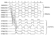
- FIG. 6 shows the operation timing of the image sensor 91a.
- SSIG represents a sub-scanning synchronization signal.
- ONSIG (R1) indicates a lighting signal (reflection color 1).
- ONSIG (R2) and ONSIG (R3) indicate a lighting signal (reflection color 2) and a lighting signal (reflection color 3), respectively.
- ONSIG (T1) indicates a lighting signal (transmission color 1).
- ONSIG (T2) and ONSIG (T3) indicate a lighting signal (transmission color 2) and a lighting signal (transmission color 3), respectively.
- OTSIG (R1) indicates an output signal (reflection color 1).
- OTSIG (R2) and OTSIG (R3) indicate an output signal (reflection color 2) and an output signal (reflection color 3), respectively.
- OTSIG (T1) indicates an output signal (transmission color 1).
- OTSIG (T2) and OTSIG (T3) indicate an output signal (transmission color 2) and an output signal (transmission color 3), respectively.
- the reflected color and transmitted color mean the wavelength of the light source.
- ON2a3a shows a waveform corresponding to the light guides 2a and 3a.
- ON2b3b indicates a waveform corresponding to the light guides 2b and 3b.
- OUT91a shows a waveform corresponding to the output of the image sensor 91a.
- ON and OFF colors are repeatedly turned on in the order of ONSIG (R1), ONSIG (T1), ONSIG (R2), ONSIG (T2), ONSIG (R3), and ONSIG (T3). Therefore, the output signal of the image sensor 91a is output in the order of OTSIG (R1), OTSIG (T1), OTSIG (R2), OTSIG (T2), OTSIG (R3), and OTSIG (T3).
- ONSIG (R1) and ONSIG (T1) will be described in detail with reference to FIG.
- the light guides 2a and 3a of the image sensor 91a are turned on, scattered and reflected by the light scattering part 21a and the light scattering part 22a, and approximately 45 degrees obliquely emitted from the light guides 2a and 3a. Is reflected by the region 17a, received by the photoelectric conversion element array 6a, and output from the image sensor 91a as an output signal of OTSIG (R1).
- the light guides 2b and 3b of the image sensor 91b are turned on according to the ONSIG (T1) lighting signal, scattered and reflected by the light scattering unit 23b, and emitted from the light guides 2a and 3a in the approximately normal direction. Passes through the region 17a, is received by the photoelectric conversion element array 6a, and is simultaneously output from the image sensor 91a as an output signal of OTSIG (T1). The same operation is performed for the reflection colors 2 and 3 and the transmission colors 2 and 3.
- a light source corresponding to the light guides 2a and 3a having a total of three types of single wavelengths and a light source corresponding to the light guides 2b and 3b having a total of three types of single wavelengths are mounted.
- a total of six types of light sources are sequentially turned on and off while being synchronized with the scanning signals, so that the outputs of the one-dimensional photoelectric conversion element array synchronized with the scanning signals and corresponding to the lighting source types are obtained in time series. be able to.
- an output can be obtained at the same timing for the image sensor 91b.
- OUT91b indicates a waveform corresponding to the output of the image sensor 91b.
- the difference in ellipsis between FIG. 6 and FIG. 7 is OUT91a and OUT91b.
- the light guide 2b of the image sensor 91b and 3b is turned off.
- the photoelectric conversion element 6a the predetermined area on the paper sheet 17 is transmitted from the photoelectric conversion element 6b at the same timing when the reflection information corresponding to the illumination wavelength from the predetermined area on the paper sheet 17 is obtained.
- transmission information corresponding to the illumination wavelength from a region that is a fixed distance away from the center is obtained.
- FIG. 5 is an overall block diagram according to Embodiment 1 of the present invention.
- ONSIG indicates a lighting signal.
- MSIG indicates a main scanning direction synchronization signal and a sub-scanning direction synchronization signal.
- the signal processing units 51a and 51b are configured as shown in FIG. 5, and the analog pixel sequential output output from the one-dimensional photoelectric conversion element arrays 6a and 6b is digitally converted by an AD converter, and then the one-dimensional photoelectric conversion element.
- Black correction processing that digitally calculates so that the black output non-uniformity characteristics of the array are uniform and the sensitivity non-uniformity characteristics of the one-dimensional photoelectric conversion element array and the output non-uniformity characteristics of the illumination system and imaging system are uniform.
- the signal is output to the outside through signal processing such as white correction processing for digital calculation.
- the lower image sensor 91a and the upper image sensor 91b are both mounted with LEDs of three different wavelengths. Not limited to this, it is also possible to use different numbers of LEDs on the top and bottom and LEDs with different wavelengths.
- the image sensor (image sensor device) according to the first embodiment uses a pair of opposed image sensors each including a reflective reading light source and a transmissive reading light source in a single housing, thereby enabling a paper sheet.
- the reflected light information and transmitted light information on both sides can be detected, and the light detection unit in the reading apparatus can be downsized without sacrificing the transport quality.
- FIG. 8 is an optical path diagram in the short direction of the light guide without cut according to the second embodiment.
- FIG. 9 is an optical path diagram in the short direction of the light guide according to the second embodiment.
- FIG. 10 is an optical path diagram in the short direction of the light guide without cut according to the second embodiment.
- FIG. 11 is an optical path diagram in the short-side direction of the light guide with two cuts according to the second embodiment.
- FIG. 12 is an optical path diagram in the short direction of the light guide with the cut direction adjusted according to the second embodiment.
- FIG. 13 is an optical path diagram in the short direction of the light guide with the cut direction adjusted according to the second embodiment.
- FIG. 14 is an optical path diagram in a short direction of a light guide body in which a light shielding member is inserted in a cut according to the second embodiment. 8 to 14, the same reference numerals are given to the same or equivalent components as those in FIG. 4, and description thereof is omitted.
- the cross section of the light guide 2 mounted on the housing 8 in Embodiment 1 was circular.
- An embodiment having a different cross-sectional shape is the second embodiment.
- the light scattering portion 21 has a small scattering angle of the light scattering portions 22 and 23 with respect to the diameter of the cross section of one light guide 2 or light guide 3, there is no particular problem.
- the scattering angle is large, the light 15 scattered and reflected from the light scattering portions 22 and 23 is emitted from the light guide 3 and incident at a certain angle with the light beam 14 incident perpendicularly to the paper sheet 17. Are overlapped on the paper sheet 17 and irradiated.
- the amount of illumination light is changed when the distance between the glass plate 1 and the paper sheet 17 changes due to a wrinkle on the paper sheet 17 or flapping during conveyance. Problems that vary greatly occur.
- FIG. 8 shows a case where the scattering angle of the light scattering portion 22 is large, and the light beam 14 and the light beam 15 are overlapped and irradiated onto the paper sheet 17. Therefore, as shown in FIG. 9, the light path 3 extends in the main scanning direction and cuts out (concave portion) 18 to block the optical path that caused the light beam 15 to spread, and the light beam 14 and the light beam 15 overlap each other. Can be prevented. That is, the light guide 3 is configured by two planes in which the side surface viewed from the sub-scanning direction intersects the side surface between the light emitting region of the light beam 14 and the light scattering portion 22 of the light beam 15, and extends in the main scanning direction. An extending cut 18 (recess) is provided.
- the cut 18 is formed by intersecting planar side walls 18 a and 18 b, the side wall 18 a and the side wall 18 b are orthogonal to each other, and the side wall 18 a of the cut 18 is parallel to the optical axis of the light beam 14.
- the light guide 3 is sub-scanned on the side surface between the light emitting region of the light flux 15 and the light scattering portion 23 of the light flux 14.
- a side surface as viewed from the direction includes two planes intersecting each other, and includes a cut 18 (concave portion) extending in the main scanning direction.
- the cut 18 is formed by intersecting planar side walls 18 a and 18 b, and the side wall 18 a and the side wall 18 b are orthogonal to each other, and the side wall 18 a of the cut 18 is parallel to the optical axis of the light beam 15.
- FIG. 10 shows a case where the scattering angles of both the light scattering portions 22 and 23 are large. At this time as well, overlapping of the luminous fluxes 14 and 15 can be prevented by making two notches 18 and 19 extending in the main scanning direction as shown in FIG. That is, the light guide 3 is provided on the side surface between the light emitting region of the light beam 14 and the light scattering portion 22 of the light beam 15 and on the side surface between the light emitting region of the light beam 15 and the light scattering portion 23 of the light beam 14, respectively. It is composed of two planes whose side surfaces viewed from the sub-scanning direction intersect, and has cuts 18 and 19 (concave portions) extending in the main scanning direction.
- the cut 18 is formed by intersecting planar side walls 18 a and 18 b, the side wall 18 a and the side wall 18 b are orthogonal to each other, and the side wall 18 a of the cut 18 is parallel to the optical axis of the light beam 14.
- the cut 19 is formed by intersecting planar side walls 19 a and 19 b, the side wall 19 a and the side wall 19 b are orthogonal to each other, and the side wall 19 a of the cut 19 is parallel to the optical axis of the light beam 15.
- the joint of the mold enters the center of the side surface of the light guide where the light beams 14 and 15 are emitted and the center of the light scattering portions 22 and 23. Therefore, a seam line may enter the light emitting portion of the light guide 3 and part of the light beams 14 and 15 may be refracted. Therefore, as a modified example, as shown in FIG. 12, by changing the angle of one of the cuts 18 and 19 extending in the main scanning direction, the mold comes out in a direction parallel to the light beam 14. You can put a line. That is, the cuts 18 and 19 are formed so that the side wall 18 a of the cut 18 and the side wall 19 b of the cut 19 are parallel to the optical axis of the light beam 14.
- the optical path 14 a is generated, the light beam 14 spreads, and may overlap the light beam 15. Therefore, as shown in FIG. 13, by making an angle with respect to the notches 18 and 19 extending on the side surface of the light guide 3, the refraction direction can be adjusted to prevent the light beams 14 and 15 from overlapping. That is, the notches 18 and 19 are formed so that the side wall 18a and the side wall 18b intersect at an obtuse angle, and the side wall 19a and the side wall 19b intersect at an obtuse angle.
- the cuts 18 and 19 are formed so that the side wall 18 a of the cut 18 and the side wall 19 b of the cut 19 are parallel to the optical axis of the light beam 14.
- the light path may be blocked by installing a light shielding member 13 extending in the main scanning direction with respect to the notches 18 and 19 of the light guide 3.
- the light shielding member 13 is made of a highly reflective material such as white resin or metal, so that the light leaking from the light guide 3 can be returned to the light guide, so that the light is more efficiently fed to the paper.
- the leaves 17 can be irradiated.
- the difference between the first embodiment and the second embodiment is the shape of the light guide.
- the shape of the housing 8 may be changed to provide the function of the light shielding member 13. Details of the image sensor (image sensor device) shown in FIGS. 15 and 16 will be described in the third embodiment.
- FIG. 15 is a cross-sectional view of the image sensor device according to the third embodiment.
- FIG. 16 is a cross-sectional view of the image sensor device according to the third embodiment.
- the same reference numerals are given to the same or equivalent components as in FIG.
- the casing 8 has a light guide 2 in which one light scattering portion 21 is installed. Two types of two light guides 3 installed were mounted. On the other hand, in the third embodiment, two light guides 3 each having two light scattering portions 22 and 23 are mounted.
- FIG. 15 shows a case where two lights emitted from the light guide 3 housed in the housing 8 are emitted in a direction perpendicular to the reflection reading position and the paper sheet 17.
- FIG. 16 shows a case where the radiation direction of one light guide 3 is installed in the reflection reading position and the transmission reading position, and the radiation direction of the other light guide is installed in the reflection reading position and the rod lens array 5 direction.
- the image sensor (image sensor device) according to the first embodiment when the light guide 2 dedicated for reflective reading is mounted as shown in FIG. 1, the light quantity emitted from the light guide 2 and the light guide 3 is used as the light source. It was necessary to adjust the current to flow, lighting time, and the number of installed light sources.
- the image sensor (image sensor device) according to Embodiment 3 since the same light guide 3 is mounted in FIGS. 15 and 16, the rod lens array 5 can be viewed from the left and right without fine adjustment. The same amount of light can be irradiated. Therefore, there is an advantage that the shadow of the read image generated when the paper sheet 17 has irregularities such as wrinkles can be easily suppressed. Moreover, since it is not necessary to create the light guide 2 dedicated for reflection, the cost can be reduced.
- FIG. 17 is an overall block diagram according to the fourth embodiment.
- 18 and 19 are timing diagrams of the image sensor according to the fourth embodiment.
- FIG. 20 is a diagram of a photoelectric conversion element array having three columns having the spectral transmission spectrum filter according to the fourth embodiment. 17 to 20, the same or equivalent components as those in FIGS. 5 to 7 are denoted by the same reference numerals, and the description thereof is omitted.
- a one-dimensional photoelectric conversion element instead of the one-dimensional photoelectric conversion element array according to the first embodiment of the present invention, as shown in FIG. 20, a one-dimensional photoelectric conversion element consisting of three columns in the direction perpendicular to the reading width direction.
- a photoelectric conversion element array having an array is mounted. Since filters having different spectral transmission spectra (here, red, green, and blue, respectively) are formed on the pixel light receiving portions of each column, the photoelectric conversion element array of each column receives optical information received by each column. Of these, only optical information having a corresponding spectral transmission spectrum can be converted into an electrical signal.
- ONSIG indicates a lighting signal as in FIG. 5, FIG. 6, and FIG. MSIG indicates a main scanning direction synchronization signal and a sub-scanning synchronization signal.
- SSIG indicates a sub-scanning synchronization signal.
- ONSIG (R1) indicates a lighting signal (reflection color 1).
- ONSIG (R2) and ONSIG (R3) indicate a lighting signal (reflection color 2) and a lighting signal (reflection color 3), respectively.
- ONSIG (T1) indicates a lighting signal (transmission color 1).
- ONSIG (T2) and ONSIG (T3) indicate a lighting signal (transmission color 2) and a lighting signal (transmission color 3), respectively.
- OTSIG (R1) indicates an output signal (reflection color 1).
- OTSIG (R2) and OTSIG (R3) indicate an output signal (reflection color 2) and an output signal (reflection color 3), respectively.
- OTSIG (T1) indicates an output signal (transmission color 1).
- OTSIG (T2) and OTSIG (T3) indicate an output signal (transmission color 2) and an output signal (transmission color 3), respectively.
- the reflected color and transmitted color mean the wavelength of the light source.
- ON2a3a shows a waveform corresponding to the light guides 2a and 3a.
- ON2b3b indicates a waveform corresponding to the light guides 2b and 3b.
- OUT91a shows a waveform corresponding to the output of the image sensor 91a.
- OUT91b shows a waveform corresponding to the output of the image sensor 91a.
- a plurality of LEDs having different emission wavelengths are mounted as light sources, but their lighting timing is different from that in the first embodiment. That is, in the first embodiment, LEDs having different wavelengths are sequentially turned on and off in chronological order, and output signals corresponding to the respective wavelengths are obtained. On the other hand, in Embodiment 4, LEDs with different wavelengths are lit simultaneously.
- FIG. 18 shows the operation timing of the image sensor 91a.
- LEDs having a total of three types of single wavelengths are mounted as light sources corresponding to the light guides 2a and 3a
- LEDs having a total of three types of single wavelengths are mounted as light sources corresponding to the light guides 2b and 3b.
- Three types of light sources corresponding to the light guides 2a and 3a are turned on at the same time
- three types of light sources corresponding to the light guides 2b and 3b are turned on at the same time, and the former and the latter perform one scanning while synchronizing with the scanning signal. It is controlled so as to be alternately turned on and off every period.
- Each one-dimensional photoelectric conversion element array having different spectral transmission spectra outputs an electrical signal proportional to the convolution integral value of the spectral sensitivity spectrum of the array and the spectrum of reflection information and transmission information received by the array.
- the reflective colors ONSIG (R1), ONSIG (R2), and ONSIG (R3) are turned on simultaneously, and then the transmission colors ONSIG (T1), ONSIG (T2), and ONSIG (T3) are turned on simultaneously. repeat. Therefore, the OTSIG (R1), OTSIG (R2), and OTSIG (R3) are simultaneously output as the output signal of the image sensor 91a, and then OTSIG (T1), OTSIG (T2), and OTSIG (T3) are simultaneously output. . This will be described in detail with reference to FIG.
- the light guides 2a and 3a of the image sensor 91a are turned on and scattered and reflected by the light scattering unit 21a and the light scattering unit 22a.
- the light having an angle of approximately 45 degrees emitted from 2a and 3a is reflected by the region 17a, received by the photoelectric conversion element array 6a, and output as an output signal from OTSIG (R1), OTSIG (R2), and OTSIG (R3). Simultaneous output from 91a.
- the light guides 2b and 3b of the image sensor 91b are turned on in accordance with the ONSIG (T1), ONSIG (T2), and ONSIG (T3) lighting signals, and are scattered and reflected by the light scattering unit 23b.
- the light in the approximately normal direction emitted from 3a passes through the region 17a, is received by the photoelectric conversion element array 6a, and is simultaneously output from the image sensor 91a as output signals of OTSIG (T1), OTSIG (T2), and OTSIG (T3). Is done. As shown in FIG. 19, an output can be obtained at the same timing for the image sensor 91b.
- the photoelectric conversion element 6b is a region away from the predetermined region on the paper sheet 17 by a certain distance at the same timing when the reflection information from the predetermined region on the paper sheet 17 is obtained from the photoelectric conversion element 6a.
- the transmission information from can be obtained.
- the signal processing units 51a and 51b are configured as shown in FIG. 17, and the three kinds of analog pixel sequential outputs output from the photoelectric conversion element arrays 6a and 6b are first multiplexed by the multiplexer unit and then the AD converter.
- Black correction processing that is digitally converted and digitally calculated so that the black output non-uniformity characteristic of each one-dimensional photoelectric conversion element array becomes uniform, and the sensitivity non-uniformity characteristics, illumination system, and imaging that the one-dimensional photoelectric conversion element array has
- the signal is output to the outside through signal processing such as white correction processing for digital calculation so that the output non-uniformity characteristic by the system becomes uniform.
- both the lower image sensor 91a and the upper image sensor 91b are mounted with LEDs of three different wavelengths.
- the types of wavelengths are not limited to this, and different numbers of LEDs may be used in different directions. It is also possible to use LEDs with wavelengths. Instead of a plurality of different LEDs, it is possible to replace them with white LEDs by phosphor excitation.
- a pair of opposed image sensors each including a reflective reading light source and a transmissive reading light source are used in a single housing, thereby allowing a paper sheet to be used.
- the reflected light information and transmitted light information on both sides can be detected, and the light detection unit in the reading apparatus can be downsized without sacrificing the transport quality.
- the pair of image sensors according to the first to fourth embodiments are arranged so as to face each other with an object to be read symmetrically with respect to the main scanning direction as an axis.
- the tilted light of the image sensor (according to the first to fourth embodiments) is reflected by the object to be read, and the normal light of the other image sensor (according to the first to fourth embodiments) is
- the optical axis of the transmitted light that has passed through the reading object is the same.
- the pair of image sensors according to the first to fourth embodiments are arranged to face each other with the object to be read being point-symmetrically about the main scanning direction.
- the first irradiation region of the image sensor (according to the first to fourth embodiments) is opposite to the second irradiation region of the other image sensor (according to the first to fourth embodiments), and the other (embodiment).
- the first irradiation region of the image sensor (according to the first to fourth) is opposite to the second irradiation region of one image sensor (according to the first to fourth embodiments), and the first irradiation region (according to the first to fourth embodiments).
- the tilted light emitted from the irradiation unit of one image sensor is the second one of the image sensor (according to the first to fourth embodiments).
- Reflected light reflected by the irradiated area and the other is combined with the transmitted light transmitted through one of the second irradiation areas of the image sensor (according to Embodiments 1 to 4).
- the rod lens array of the other image sensor forms an image, and the inclined light irradiated from the irradiation unit of the other (according to the first to fourth embodiments)
- the reflected light reflected by the second irradiation region of the image sensor (according to the first to fourth embodiments) and the normal light emitted from the irradiation unit of one image sensor (according to the first to fourth embodiments) are the other.
- the combined light is combined with the transmitted light transmitted through the second irradiation region of the image sensor (according to the first to fourth embodiments).
Abstract
Description
以下、この発明の実施の形態1に係るイメージセンサおよびイメージセンサ装置について説明する。図1は、実施の形態1に係るイメージセンサ装置の断面図である。本発明の実施の形態において、17はイメージセンサ装置の外部にある、読み取られるべき紙幣、有価証券、小切手などの紙葉であって、反射光情報と透かしなどの透過光情報を有するものである。
Hereinafter, an image sensor and an image sensor device according to
以下、実施の形態2に係るイメージセンサおよびイメージセンサ装置について説明する。図8は、実施の形態2に係る切れ込みのない導光体の短手方向への光路図である。図9は、実施の形態2に係る導光体の短手方向への光路図である。図10は、実施の形態2に係る切れ込みのない導光体の短手方向への光路図である。図11は、実施の形態2に係る切れ込みを2つ入れた導光体の短手方向への光路図である。図12は、実施の形態2に係る切れ込みの方向を調整した導光体の短手方向への光路図である。図13は、実施の形態2に係る切れ込みの方向を調整した導光体の短手方向への光路図である。図14は、実施の形態2に係る切れ込みに遮光部材を入れた導光体の短手方向への光路図である。図8から図14において、図4と同一若しくは同等の構成要素には同一符号を付し、その説明を省略する。 Embodiment 2. FIG.
Hereinafter, an image sensor and an image sensor device according to the second embodiment will be described. FIG. 8 is an optical path diagram in the short direction of the light guide without cut according to the second embodiment. FIG. 9 is an optical path diagram in the short direction of the light guide according to the second embodiment. FIG. 10 is an optical path diagram in the short direction of the light guide without cut according to the second embodiment. FIG. 11 is an optical path diagram in the short-side direction of the light guide with two cuts according to the second embodiment. FIG. 12 is an optical path diagram in the short direction of the light guide with the cut direction adjusted according to the second embodiment. FIG. 13 is an optical path diagram in the short direction of the light guide with the cut direction adjusted according to the second embodiment. FIG. 14 is an optical path diagram in a short direction of a light guide body in which a light shielding member is inserted in a cut according to the second embodiment. 8 to 14, the same reference numerals are given to the same or equivalent components as those in FIG. 4, and description thereof is omitted.
以下、この発明の形態3に係るイメージセンサおよびイメージセンサ装置について説明する。図15は、実施の形態3係るイメージセンサ装置の断面図である。図16は、実施の形態3係るイメージセンサ装置の断面図である。図15、図16において、図1と同一若しくは同等の構成要素には同一符号を付し、その説明を省略する。
Hereinafter, an image sensor and an image sensor device according to
以下、この発明の形態4に係るイメージセンサおよびイメージセンサ装置について説明する。図17は、実施の形態4に係る全体ブロック図である。図18、図19は、実施の形態4に係るイメージセンサのタイミング図である。図20は、実施の形態4に係る分光透過スペクトルフィルタを持つ3列からなる光電変換素子アレイの図である。図17から図20において、図5から図7と同一若しくは同等の構成要素には同一符号を付し、その説明を省略する。
Hereinafter, an image sensor and an image sensor device according to
2 導光体
3 導光体
5 ロッドレンズアレイ
6 光電変換素子アレイ
7 プリント基板
8 筐体
9 フレキシブルプリント基板
10 ホルダ
11 フレキシブルプリント基板
12 ホルダ
13 遮光部材
14 光束
14a 光束
15 光束
16 継ぎ目線
17 紙葉
17a 紙葉17の領域
17b 紙葉17の領域
18 切れ込み(凹部)
18a 切れ込み18の側壁
18b 切れ込み18の側壁
19 切れ込み(凹部)
19a 切れ込み19の側壁
19b 切れ込み19の側壁
20 ローラー
21~23 光散乱部(光反射パターン)
41~44 光源実装部
63 青フィルタ付き一次元光電変換素子アレイ
64 緑フィルタ付き一次元光電変換素子アレイ
65 赤フィルタ付き一次元光電変換素子アレイ
51 信号処理部
91 イメージセンサ DESCRIPTION OF
41 to 44 Light
Claims (15)
- 被読取物に光を照射する主走査方向に延在する照明部と、前記被読取物からの光を結像するロッドレンズアレイと、このロッドレンズアレイで結像された光を電気信号に変換する受光部とを備え、
前記照明部は、前記被読取物の第1照射領域を照射する前記被読取物の法線方向からの法線光と前記第1照射領域から副走査方向に離れた第2照射領域を照射する前記被読取物の法線方向から所定の角度だけ傾斜させた傾斜光とを照射するイメージセンサ。 An illumination unit extending in the main scanning direction for irradiating the object to be read, a rod lens array for forming an image of light from the object to be read, and converting the light imaged by the rod lens array into an electrical signal And a light receiving unit that
The illumination unit irradiates normal light from the normal direction of the read object that irradiates the first irradiation area of the read object and a second irradiation area that is separated from the first irradiation area in the sub-scanning direction. An image sensor that irradiates inclined light inclined by a predetermined angle from a normal line direction of the reading object. - 前記照明部は、主走査方向に延在する棒状の導光体と、この導光体の主走査方向の端部に設けられ前記導光体の端部に光を照射する光源と、前記導光体の端部から入射した光を反射及び散乱させて主走査方向へ伝搬させると共に前記導光体の光出射領域から光を出射する主走査方向に2列の反射領域を有する光反射パターンとを備え、
一方の列の前記光反射パターンが前記傾斜光を出射し、他方の列の前記光反射パターンが前記法線光を出射する請求項1に記載のイメージセンサ。 The illumination unit includes a rod-shaped light guide that extends in the main scanning direction, a light source that is provided at an end of the light guide in the main scanning direction, and that irradiates light to the end of the light guide, and the light guide. A light reflection pattern that reflects and scatters light incident from the end of the light body and propagates it in the main scanning direction, and has two rows of reflection areas in the main scanning direction to emit light from the light emitting area of the light guide; With
The image sensor according to claim 1, wherein the light reflection pattern in one row emits the inclined light, and the light reflection pattern in the other row emits the normal light. - 前記導光体は、前記法線光の光出射領域と前記傾斜光の光反射パターンとの間の側面に、副走査方向から見た側面が交差する2つの平面で構成され、主走査方向に延在する凹部を備えた請求項2に記載のイメージセンサ。 The light guide is composed of two planes whose side surfaces viewed from the sub-scanning direction intersect with the side surfaces between the light emitting region of the normal light and the light reflection pattern of the inclined light, and in the main scanning direction. The image sensor according to claim 2, further comprising an extending recess.
- 前記導光体は、前記傾斜光の光出射領域と前記法線光の光反射パターンとの間の側面に、副走査方向から見た側面が交差する2つの平面で構成され、主走査方向に延在する凹部を備えた請求項2に記載のイメージセンサ。 The light guide is composed of two planes whose side surfaces viewed from the sub-scanning direction intersect with the side surfaces between the light emission region of the inclined light and the light reflection pattern of the normal light, and in the main scanning direction. The image sensor according to claim 2, further comprising an extending recess.
- 前記導光体は、前記法線光の光出射領域と前記傾斜光の光反射パターンとの間の側面及び前記傾斜光の光出射領域と前記法線光の光反射パターンとの間の側面に、それぞれ副走査方向から見た側面が交差する2つの平面で構成され、主走査方向に延在する凹部を備えた請求項2に記載のイメージセンサ。 The light guide is disposed on a side surface between the light emitting region of the normal light and the light reflection pattern of the inclined light and on a side surface between the light emitting region of the inclined light and the light reflection pattern of the normal light. The image sensor according to claim 2, further comprising: a concave portion that is configured by two planes intersecting each other when viewed from the sub-scanning direction and extends in the main scanning direction.
- 前記導光体の前記法線光の光出射領域と前記傾斜光の光反射パターンとの間の側面に設けられた主走査方向に延在する凹部の副走査方向から見た側面の一方の平面が、前記法線光の光軸に平行である請求項3又は請求項5に記載のイメージセンサ。 One plane of the side surface seen from the sub-scanning direction of the concave portion extending in the main scanning direction provided on the side surface between the light emitting region of the normal light and the light reflection pattern of the inclined light of the light guide. The image sensor according to claim 3, wherein is parallel to an optical axis of the normal light.
- 前記導光体の前記傾斜光の光出射領域と前記法線光の光反射パターンとの間の側面に設けられた主走査方向に延在する凹部の副走査方向から見た側面の一方の平面が、前記傾斜光の光軸に平行である請求項4又は請求項5に記載のイメージセンサ。 One plane of the side surface seen from the sub-scanning direction of the recess extending in the main scanning direction provided on the side surface between the light emitting region of the inclined light and the light reflection pattern of the normal light of the light guide The image sensor according to claim 4, wherein is parallel to the optical axis of the tilted light.
- 前記導光体の前記法線光の光出射領域と前記傾斜光の光反射パターンとの間の側面に設けられた主走査方向に延在する凹部の副走査方向から見た側面の一方の平面が、前記法線光の光軸に平行であり、前記導光体の前記傾斜光の光出射領域と前記法線光の光反射パターンとの間の側面に設けられた主走査方向に延在する凹部の副走査方向から見た側面の一方の平面が、前記傾斜光の光軸に平行である請求項5に記載のイメージセンサ。 One plane of the side surface seen from the sub-scanning direction of the concave portion extending in the main scanning direction provided on the side surface between the light emitting region of the normal light and the light reflection pattern of the inclined light of the light guide. Is parallel to the optical axis of the normal light and extends in the main scanning direction provided on a side surface between the light emitting region of the inclined light and the light reflection pattern of the normal light of the light guide. The image sensor according to claim 5, wherein one of the side surfaces of the concave portion viewed from the sub-scanning direction is parallel to the optical axis of the inclined light.
- 前記凹部は、交差する平面の交差角度が90度である請求項8に記載のイメージセンサ。 The image sensor according to claim 8, wherein the concave portion has an intersecting angle of 90 degrees with a plane intersecting.
- 前記凹部は、交差する平面の交差角度が鈍角である請求項8に記載のイメージセンサ。 The image sensor according to claim 8, wherein the concave portion has an obtuse angle with respect to an intersecting plane.
- 前記凹部に、遮光部材を配置した請求項9に記載のイメージセンサ。 The image sensor according to claim 9, wherein a light shielding member is disposed in the concave portion.
- 互いに波長の異なる複数の前記光源と、主走査方向に複数列の光電変換素子群を有する前記受光部とを備え、
前記複数列の光電変換素子上には、列毎に互いに異なる透過スペクトルを有するフィルタが形成されるとともに、列単位で光電変換信号を読み出す請求項1から請求項11のいずれかに記載のイメージセンサ。 A plurality of light sources having different wavelengths from each other, and the light receiving unit having a plurality of rows of photoelectric conversion elements in the main scanning direction,
12. The image sensor according to claim 1, wherein filters having different transmission spectra for each column are formed on the plurality of columns of photoelectric conversion elements, and photoelectric conversion signals are read out in units of columns. . - 蛍光体励起による白色光源と、主走査方向に複数列の光電変換素子群を有する前記受光部とを備え、
前記複数列の光電変換素子上には、列毎に互いに異なる透過スペクトルを有するフィルタが形成されるとともに、列単位で光電変換信号を読み出す請求項1から請求項11のいずれかに記載のイメージセンサ。 A white light source by phosphor excitation, and the light receiving unit having a plurality of rows of photoelectric conversion elements in the main scanning direction,
12. The image sensor according to claim 1, wherein filters having different transmission spectra for each column are formed on the plurality of columns of photoelectric conversion elements, and photoelectric conversion signals are read out in units of columns. . - 請求項1から請求項13のいずれかに記載のイメージセンサの対が主走査方向を軸に点対称に被読取物を挟んで対向して配置され、一方のイメージセンサの前記傾斜光が前記被読取物で反射した反射光の光軸と、他方のイメージセンサの前記法線光が前記被読取物を透過した透過光の光軸とが一致しているイメージセンサ装置。 A pair of image sensors according to any one of claims 1 to 13 are arranged to face each other with an object to be read symmetrically with respect to a main scanning direction as an axis, and the inclined light of one image sensor An image sensor device in which an optical axis of reflected light reflected by a reading object coincides with an optical axis of transmitted light obtained by transmitting the normal light of the other image sensor through the object to be read.
- 請求項1から請求項13のいずれかに記載のイメージセンサの対が主走査方向を軸に点対称に被読取物を挟んで対向して配置され、一方のイメージセンサの第1照射領域は他方のイメージセンサの第2照射領域の反対側であり、他方のイメージセンサの第1照射領域は一方のイメージセンサの第2照射領域の反対側であり、一方のイメージセンサのロッドレンズアレイは、一方のイメージセンサの照射部から照射された傾斜光が一方のイメージセンサの第2照射領域で反射された反射光と他方のイメージセンサの照射部から照射された法線光が一方のイメージセンサの第2照射領域を透過してきた透過光との合成光を結像し、他方のイメージセンサのロッドレンズアレイは、他方のイメージセンサの照射部から照射された傾斜光が他方のイメージセンサの第2照射領域で反射された反射光と一方のイメージセンサの照射部から照射された法線光が他方のイメージセンサの第2照射領域を透過してきた透過光との合成光を結像するイメージセンサ装置。 The pair of image sensors according to any one of claims 1 to 13 are arranged to face each other with a reading object in a point symmetry with respect to the main scanning direction, and the first irradiation region of one image sensor is the other. The image sensor is opposite to the second irradiation area of the image sensor, the first irradiation area of the other image sensor is opposite to the second irradiation area of one image sensor, and the rod lens array of one image sensor is The reflected light reflected from the second irradiation area of one image sensor and the normal light emitted from the irradiation part of the other image sensor are the first light of the first image sensor. 2 The combined light with the transmitted light that has passed through the irradiation area is imaged, and the rod lens array of the other image sensor has the inclined light emitted from the irradiation part of the other image sensor. Imaging the combined light of the reflected light reflected by the second irradiation area of the image sensor and the transmitted light transmitted through the second irradiation area of the other image sensor by the normal light emitted from the irradiation part of one image sensor An image sensor device.
Priority Applications (4)
| Application Number | Priority Date | Filing Date | Title |
|---|---|---|---|
| JP2014541953A JP6308947B2 (en) | 2012-10-18 | 2013-10-17 | Image sensor device |
| CN201380054514.9A CN104737525B (en) | 2012-10-18 | 2013-10-17 | Image sensor apparatus |
| EP13847212.1A EP2911379B1 (en) | 2012-10-18 | 2013-10-17 | Image sensor and image sensor device |
| US14/433,739 US9385150B2 (en) | 2012-10-18 | 2013-10-17 | Image sensor device |
Applications Claiming Priority (4)
| Application Number | Priority Date | Filing Date | Title |
|---|---|---|---|
| JP2012231051 | 2012-10-18 | ||
| JP2012-231051 | 2012-10-18 | ||
| JP2013045670 | 2013-03-07 | ||
| JP2013-045670 | 2013-03-07 |
Publications (1)
| Publication Number | Publication Date |
|---|---|
| WO2014061274A1 true WO2014061274A1 (en) | 2014-04-24 |
Family
ID=50487853
Family Applications (1)
| Application Number | Title | Priority Date | Filing Date |
|---|---|---|---|
| PCT/JP2013/006171 WO2014061274A1 (en) | 2012-10-18 | 2013-10-17 | Image sensor and image sensor device |
Country Status (5)
| Country | Link |
|---|---|
| US (1) | US9385150B2 (en) |
| EP (1) | EP2911379B1 (en) |
| JP (2) | JP6308947B2 (en) |
| CN (2) | CN104737525B (en) |
| WO (1) | WO2014061274A1 (en) |
Cited By (10)
| Publication number | Priority date | Publication date | Assignee | Title |
|---|---|---|---|---|
| CN104580806A (en) * | 2015-01-20 | 2015-04-29 | 威海华菱光电股份有限公司 | Image reader |
| WO2015178384A1 (en) * | 2014-05-22 | 2015-11-26 | グローリー株式会社 | Fluorescence/phosphorescence detection device |
| WO2016052749A1 (en) * | 2014-10-03 | 2016-04-07 | グローリー株式会社 | Paper sheet identification device and paper sheet identification method |
| JP2016110303A (en) * | 2014-12-04 | 2016-06-20 | 沖電気工業株式会社 | Paper sheet discrimination device and automatic transaction device including the same |
| JP2016170225A (en) * | 2015-03-11 | 2016-09-23 | 京セラドキュメントソリューションズ株式会社 | Illumination device, image reader including the same, and light guide member |
| JP2018098595A (en) * | 2016-12-12 | 2018-06-21 | ウシオ電機株式会社 | Linear light source device |
| CN109565531A (en) * | 2016-08-08 | 2019-04-02 | 日本电产三协株式会社 | Information read device |
| WO2020008944A1 (en) * | 2018-07-05 | 2020-01-09 | 三菱電機株式会社 | Lighting device and image reading device |
| WO2020129437A1 (en) * | 2018-12-18 | 2020-06-25 | 三菱電機株式会社 | Image reading device |
| JP2021022776A (en) * | 2019-07-25 | 2021-02-18 | キヤノン株式会社 | Image reading device and image forming device |
Families Citing this family (14)
| Publication number | Priority date | Publication date | Assignee | Title |
|---|---|---|---|---|
| DE112013006158B4 (en) | 2012-12-20 | 2023-04-06 | Mitsubishi Electric Corporation | Light guide, light source device and image reading device |
| CN105247582B (en) | 2013-04-30 | 2017-11-28 | 光荣株式会社 | Image capturing device and image acquisition method |
| JP6278761B2 (en) * | 2014-03-11 | 2018-02-14 | キヤノン株式会社 | Reading control apparatus and reading control method |
| WO2015141461A1 (en) * | 2014-03-17 | 2015-09-24 | 三菱電機株式会社 | Lighting apparatus and image reading apparatus |
| CN108989598B (en) * | 2017-05-30 | 2019-12-17 | 精工爱普生株式会社 | scanner and method for producing scanned data |
| WO2019003480A1 (en) | 2017-06-28 | 2019-01-03 | 三菱電機株式会社 | Light guide body and image reading apparatus |
| JP6395988B1 (en) * | 2017-06-28 | 2018-09-26 | 三菱電機株式会社 | Light guide and image reading apparatus |
| JP6972945B2 (en) * | 2017-11-10 | 2021-11-24 | セイコーエプソン株式会社 | Reader, image processing program and image production method |
| WO2019138878A1 (en) * | 2018-01-11 | 2019-07-18 | 三菱電機株式会社 | Capacitance detection device and image reading device |
| DE102018103630A1 (en) * | 2018-02-19 | 2019-08-22 | Bundesdruckerei Gmbh | Device and method for optically examining a security document, in particular a passbook |
| KR101977634B1 (en) * | 2018-09-28 | 2019-08-28 | 주식회사 카스모아이티 | Counterfeit Bill Detection Sensor Module With Diagonal Image Sensors |
| JP7461172B2 (en) * | 2020-03-02 | 2024-04-03 | グローリー株式会社 | Illumination device for image sensors |
| CN113973159A (en) * | 2021-11-24 | 2022-01-25 | 威海华菱光电股份有限公司 | Image scanning system and scanning method |
| JP2023173165A (en) * | 2022-05-25 | 2023-12-07 | 株式会社リコー | Illuminating device and image reading device |
Citations (6)
| Publication number | Priority date | Publication date | Assignee | Title |
|---|---|---|---|---|
| JPH09261409A (en) * | 1996-03-19 | 1997-10-03 | Pfu Ltd | Optical device for color image reader |
| JP2009135914A (en) * | 2007-10-31 | 2009-06-18 | Canon Electronics Inc | Image reading apparatus and control method therefor, as well as, storage medium |
| JP4424360B2 (en) | 2007-02-26 | 2010-03-03 | 三菱電機株式会社 | Image sensor |
| JP2011044336A (en) * | 2009-08-21 | 2011-03-03 | Ushio Inc | Light source device |
| JP2011182370A (en) * | 2010-03-04 | 2011-09-15 | Ushio Inc | Light source device |
| JP2011188231A (en) * | 2010-03-09 | 2011-09-22 | Panasonic Corp | Image reading apparatus |
Family Cites Families (10)
| Publication number | Priority date | Publication date | Assignee | Title |
|---|---|---|---|---|
| JPS60146386A (en) * | 1984-01-11 | 1985-08-02 | 株式会社東芝 | Sheet papers discriminator |
| JP3936438B2 (en) * | 1997-07-31 | 2007-06-27 | ローム株式会社 | Image reading device |
| JP2001320551A (en) * | 2000-05-12 | 2001-11-16 | Canon Inc | Device and method for reading image and computer readable storage medium |
| JP2004326624A (en) * | 2003-04-25 | 2004-11-18 | Aruze Corp | Discrimination sensor |
| JP4522952B2 (en) * | 2006-01-18 | 2010-08-11 | 三菱電機株式会社 | Image reading device |
| JP2007249475A (en) * | 2006-03-15 | 2007-09-27 | Mitsubishi Electric Corp | Image reader and bill reading method |
| JP4396715B2 (en) * | 2007-03-01 | 2010-01-13 | 三菱電機株式会社 | Image sensor |
| CN101809631B (en) * | 2007-09-27 | 2012-07-25 | 光荣株式会社 | Paper sheet processor |
| JP4609531B2 (en) * | 2008-06-11 | 2011-01-12 | 三菱電機株式会社 | Image reading device |
| JP5268667B2 (en) * | 2009-01-16 | 2013-08-21 | ローレル機械株式会社 | Banknote handling machine |
-
2013
- 2013-10-17 WO PCT/JP2013/006171 patent/WO2014061274A1/en active Application Filing
- 2013-10-17 US US14/433,739 patent/US9385150B2/en active Active
- 2013-10-17 CN CN201380054514.9A patent/CN104737525B/en active Active
- 2013-10-17 JP JP2014541953A patent/JP6308947B2/en active Active
- 2013-10-17 EP EP13847212.1A patent/EP2911379B1/en active Active
- 2013-10-17 CN CN201710707028.2A patent/CN107293036B/en active Active
-
2017
- 2017-02-14 JP JP2017024552A patent/JP6628753B2/en active Active
Patent Citations (6)
| Publication number | Priority date | Publication date | Assignee | Title |
|---|---|---|---|---|
| JPH09261409A (en) * | 1996-03-19 | 1997-10-03 | Pfu Ltd | Optical device for color image reader |
| JP4424360B2 (en) | 2007-02-26 | 2010-03-03 | 三菱電機株式会社 | Image sensor |
| JP2009135914A (en) * | 2007-10-31 | 2009-06-18 | Canon Electronics Inc | Image reading apparatus and control method therefor, as well as, storage medium |
| JP2011044336A (en) * | 2009-08-21 | 2011-03-03 | Ushio Inc | Light source device |
| JP2011182370A (en) * | 2010-03-04 | 2011-09-15 | Ushio Inc | Light source device |
| JP2011188231A (en) * | 2010-03-09 | 2011-09-22 | Panasonic Corp | Image reading apparatus |
Cited By (24)
| Publication number | Priority date | Publication date | Assignee | Title |
|---|---|---|---|---|
| CN106463010A (en) * | 2014-05-22 | 2017-02-22 | 光荣株式会社 | Fluorescence/phosphorescence detection device |
| WO2015178384A1 (en) * | 2014-05-22 | 2015-11-26 | グローリー株式会社 | Fluorescence/phosphorescence detection device |
| JP2015222463A (en) * | 2014-05-22 | 2015-12-10 | グローリー株式会社 | Fluorescent light and phosphorescence detection device |
| EP3147873B1 (en) | 2014-05-22 | 2022-09-28 | Glory Ltd. | Fluorescence/phosphorescence detection device |
| WO2016052749A1 (en) * | 2014-10-03 | 2016-04-07 | グローリー株式会社 | Paper sheet identification device and paper sheet identification method |
| JPWO2016052749A1 (en) * | 2014-10-03 | 2017-07-13 | グローリー株式会社 | Paper sheet identification device and paper sheet identification method |
| EP3203449A4 (en) * | 2014-10-03 | 2018-05-30 | Glory Ltd. | Paper sheet identification device and paper sheet identification method |
| JP2016110303A (en) * | 2014-12-04 | 2016-06-20 | 沖電気工業株式会社 | Paper sheet discrimination device and automatic transaction device including the same |
| CN104580806B (en) * | 2015-01-20 | 2018-03-23 | 威海华菱光电股份有限公司 | Cis |
| CN104580806A (en) * | 2015-01-20 | 2015-04-29 | 威海华菱光电股份有限公司 | Image reader |
| JP2016170225A (en) * | 2015-03-11 | 2016-09-23 | 京セラドキュメントソリューションズ株式会社 | Illumination device, image reader including the same, and light guide member |
| CN109565531A (en) * | 2016-08-08 | 2019-04-02 | 日本电产三协株式会社 | Information read device |
| JP2018098595A (en) * | 2016-12-12 | 2018-06-21 | ウシオ電機株式会社 | Linear light source device |
| WO2020008944A1 (en) * | 2018-07-05 | 2020-01-09 | 三菱電機株式会社 | Lighting device and image reading device |
| JPWO2020008944A1 (en) * | 2018-07-05 | 2020-07-09 | 三菱電機株式会社 | Lighting device and image reading device |
| EP3820132A4 (en) * | 2018-07-05 | 2021-07-07 | Mitsubishi Electric Corporation | Lighting device and image reading device |
| US11233917B2 (en) | 2018-07-05 | 2022-01-25 | Mitsubishi Electric Corporation | Lighting device and image reading device |
| DE112019006268T5 (en) | 2018-12-18 | 2021-09-09 | Mitsubishi Electric Corporation | Image reading device |
| JPWO2020129437A1 (en) * | 2018-12-18 | 2021-09-09 | 三菱電機株式会社 | Image reader |
| JP7023383B2 (en) | 2018-12-18 | 2022-02-21 | 三菱電機株式会社 | Image reader |
| WO2020129437A1 (en) * | 2018-12-18 | 2020-06-25 | 三菱電機株式会社 | Image reading device |
| US11750754B2 (en) | 2018-12-18 | 2023-09-05 | Mitsubishi Electric Corporation | Image reading device controlling exposure time by multiple opening and closing operations of electronic shutters |
| JP2021022776A (en) * | 2019-07-25 | 2021-02-18 | キヤノン株式会社 | Image reading device and image forming device |
| JP7346126B2 (en) | 2019-07-25 | 2023-09-19 | キヤノン株式会社 | Image reading device and image forming device |
Also Published As
| Publication number | Publication date |
|---|---|
| CN104737525B (en) | 2017-09-08 |
| EP2911379A4 (en) | 2016-06-01 |
| US20150249104A1 (en) | 2015-09-03 |
| US9385150B2 (en) | 2016-07-05 |
| EP2911379A1 (en) | 2015-08-26 |
| CN107293036A (en) | 2017-10-24 |
| JP6628753B2 (en) | 2020-01-15 |
| JP6308947B2 (en) | 2018-04-11 |
| CN107293036B (en) | 2019-08-30 |
| EP2911379B1 (en) | 2020-02-26 |
| JPWO2014061274A1 (en) | 2016-09-05 |
| CN104737525A (en) | 2015-06-24 |
| JP2017085670A (en) | 2017-05-18 |
Similar Documents
| Publication | Publication Date | Title |
|---|---|---|
| JP6308947B2 (en) | Image sensor device | |
| JP4609531B2 (en) | Image reading device | |
| RU2169393C2 (en) | Device and method for checking sheet material including bank notes and securities | |
| JP5518820B2 (en) | Image sensor unit and image reading apparatus | |
| US7682040B2 (en) | Optical system for creating an illuminated strip | |
| US7635830B2 (en) | Optical system for forming an illuminated pattern on a material in motion and which illuminated pattern is synchronized with a detection device | |
| CN109804238B (en) | Optical inspection device | |
| JP5755144B2 (en) | Work inspection device | |
| JP6579863B2 (en) | Reader and transmission light source unit | |
| RU2318240C2 (en) | Device for checking banknotes | |
| JP5820845B2 (en) | Illumination device, image sensor unit, and paper sheet identification device | |
| JP4805534B2 (en) | Work inspection device | |
| US9894233B2 (en) | Lighting apparatus and image reading apparatus | |
| JP2009133743A (en) | Hologram inspection apparatus | |
| JP7392470B2 (en) | Lighting for inspecting defects in sheet-like objects and defect inspection device for sheet-like objects | |
| JP5100149B2 (en) | Optical fiber illuminator and hologram inspection apparatus provided with the same | |
| JP2016163146A (en) | Device | |
| JP2004355263A (en) | Image detector for paper currency | |
| JP2009145183A (en) | Foreign matter detector, foreign matter detecting method, and paper sheet processor | |
| JPH07283907A (en) | Illuminating optical device |
Legal Events
| Date | Code | Title | Description |
|---|---|---|---|
| 121 | Ep: the epo has been informed by wipo that ep was designated in this application |
Ref document number: 13847212 Country of ref document: EP Kind code of ref document: A1 |
|
| ENP | Entry into the national phase |
Ref document number: 2014541953 Country of ref document: JP Kind code of ref document: A |
|
| WWE | Wipo information: entry into national phase |
Ref document number: 14433739 Country of ref document: US |
|
| WWE | Wipo information: entry into national phase |
Ref document number: 2013847212 Country of ref document: EP |
|
| NENP | Non-entry into the national phase |
Ref country code: DE |