WO2013145311A1 - Rfid tag - Google Patents
Rfid tag Download PDFInfo
- Publication number
- WO2013145311A1 WO2013145311A1 PCT/JP2012/058733 JP2012058733W WO2013145311A1 WO 2013145311 A1 WO2013145311 A1 WO 2013145311A1 JP 2012058733 W JP2012058733 W JP 2012058733W WO 2013145311 A1 WO2013145311 A1 WO 2013145311A1
- Authority
- WO
- WIPO (PCT)
- Prior art keywords
- rfid tag
- antenna
- loop
- substrate
- vias
- Prior art date
Links
Images


Classifications
-
- G—PHYSICS
- G06—COMPUTING; CALCULATING OR COUNTING
- G06K—GRAPHICAL DATA READING; PRESENTATION OF DATA; RECORD CARRIERS; HANDLING RECORD CARRIERS
- G06K19/00—Record carriers for use with machines and with at least a part designed to carry digital markings
- G06K19/06—Record carriers for use with machines and with at least a part designed to carry digital markings characterised by the kind of the digital marking, e.g. shape, nature, code
- G06K19/067—Record carriers with conductive marks, printed circuits or semiconductor circuit elements, e.g. credit or identity cards also with resonating or responding marks without active components
- G06K19/07—Record carriers with conductive marks, printed circuits or semiconductor circuit elements, e.g. credit or identity cards also with resonating or responding marks without active components with integrated circuit chips
- G06K19/077—Constructional details, e.g. mounting of circuits in the carrier
- G06K19/07749—Constructional details, e.g. mounting of circuits in the carrier the record carrier being capable of non-contact communication, e.g. constructional details of the antenna of a non-contact smart card
- G06K19/0775—Constructional details, e.g. mounting of circuits in the carrier the record carrier being capable of non-contact communication, e.g. constructional details of the antenna of a non-contact smart card arrangements for connecting the integrated circuit to the antenna
- G06K19/07754—Constructional details, e.g. mounting of circuits in the carrier the record carrier being capable of non-contact communication, e.g. constructional details of the antenna of a non-contact smart card arrangements for connecting the integrated circuit to the antenna the connection being galvanic
-
- H—ELECTRICITY
- H01—ELECTRIC ELEMENTS
- H01Q—ANTENNAS, i.e. RADIO AERIALS
- H01Q1/00—Details of, or arrangements associated with, antennas
- H01Q1/36—Structural form of radiating elements, e.g. cone, spiral, umbrella; Particular materials used therewith
- H01Q1/38—Structural form of radiating elements, e.g. cone, spiral, umbrella; Particular materials used therewith formed by a conductive layer on an insulating support
-
- G—PHYSICS
- G06—COMPUTING; CALCULATING OR COUNTING
- G06K—GRAPHICAL DATA READING; PRESENTATION OF DATA; RECORD CARRIERS; HANDLING RECORD CARRIERS
- G06K19/00—Record carriers for use with machines and with at least a part designed to carry digital markings
- G06K19/06—Record carriers for use with machines and with at least a part designed to carry digital markings characterised by the kind of the digital marking, e.g. shape, nature, code
- G06K19/067—Record carriers with conductive marks, printed circuits or semiconductor circuit elements, e.g. credit or identity cards also with resonating or responding marks without active components
- G06K19/07—Record carriers with conductive marks, printed circuits or semiconductor circuit elements, e.g. credit or identity cards also with resonating or responding marks without active components with integrated circuit chips
- G06K19/077—Constructional details, e.g. mounting of circuits in the carrier
- G06K19/07749—Constructional details, e.g. mounting of circuits in the carrier the record carrier being capable of non-contact communication, e.g. constructional details of the antenna of a non-contact smart card
- G06K19/07773—Antenna details
- G06K19/07786—Antenna details the antenna being of the HF type, such as a dipole
-
- H—ELECTRICITY
- H01—ELECTRIC ELEMENTS
- H01Q—ANTENNAS, i.e. RADIO AERIALS
- H01Q1/00—Details of, or arrangements associated with, antennas
- H01Q1/12—Supports; Mounting means
- H01Q1/22—Supports; Mounting means by structural association with other equipment or articles
- H01Q1/2208—Supports; Mounting means by structural association with other equipment or articles associated with components used in interrogation type services, i.e. in systems for information exchange between an interrogator/reader and a tag/transponder, e.g. in Radio Frequency Identification [RFID] systems
- H01Q1/2225—Supports; Mounting means by structural association with other equipment or articles associated with components used in interrogation type services, i.e. in systems for information exchange between an interrogator/reader and a tag/transponder, e.g. in Radio Frequency Identification [RFID] systems used in active tags, i.e. provided with its own power source or in passive tags, i.e. deriving power from RF signal
-
- H—ELECTRICITY
- H01—ELECTRIC ELEMENTS
- H01Q—ANTENNAS, i.e. RADIO AERIALS
- H01Q5/00—Arrangements for simultaneous operation of antennas on two or more different wavebands, e.g. dual-band or multi-band arrangements
- H01Q5/30—Arrangements for providing operation on different wavebands
- H01Q5/307—Individual or coupled radiating elements, each element being fed in an unspecified way
- H01Q5/314—Individual or coupled radiating elements, each element being fed in an unspecified way using frequency dependent circuits or components, e.g. trap circuits or capacitors
- H01Q5/321—Individual or coupled radiating elements, each element being fed in an unspecified way using frequency dependent circuits or components, e.g. trap circuits or capacitors within a radiating element or between connected radiating elements
-
- H—ELECTRICITY
- H01—ELECTRIC ELEMENTS
- H01Q—ANTENNAS, i.e. RADIO AERIALS
- H01Q7/00—Loop antennas with a substantially uniform current distribution around the loop and having a directional radiation pattern in a plane perpendicular to the plane of the loop
Definitions
- the present invention relates to an RFID (Radio Frequency Identifier) tag.
- the conventional antenna device has not been sufficiently reduced in cost.
- An RFID tag includes a substrate, a pair of first antenna elements formed on one surface of the substrate, an IC chip connected between the pair of first antenna elements, A second antenna element formed on the other surface of the substrate; and formed between the pair of first antenna elements and the second antenna element; the pair of first antenna elements; the IC chip; A pair of first connection portions that form a first loop with two antenna elements, and the pair of first antenna elements, the IC chip, formed between the pair of first antenna elements and the second antenna element, And the second antenna element and a pair of second connection portions that form a second loop longer than the first loop, The length of flops and the second loop are each shorter than the wavelength at the operating frequency.
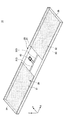
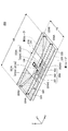
- FIG. 6 is a perspective perspective view showing RFID tags 10 and 10A of Comparative Example 1.
- FIG. 6 is a perspective perspective view showing RFID tags 10 and 10A of Comparative Example 1.
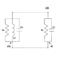
- FIG. 6 is a diagram showing an equivalent circuit of the RFID tag 10 of Comparative Example 1.
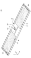
- FIG. 10 is a perspective perspective view showing RFID tags 10B and 10C of Comparative Example 2.
- FIG. 10 is a perspective perspective view showing RFID tags 10B and 10C of Comparative Example 2.
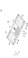
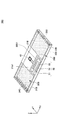
- 1 is a perspective perspective view showing an RFID tag 100 according to Embodiment 1.
- FIG. 2 is a diagram illustrating an equivalent circuit of the RFID tag 100 according to Embodiment 1.
- FIG. 5 is a perspective perspective view showing an RFID tag 200 of a second embodiment.
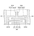
- 6 is an enlarged view showing a capacitor 240 of the RFID tag 200 according to Embodiment 2.
- FIG. 6 is an enlarged view of a capacitor 50 of an RFID tag 10B of Comparative Example 2.
- FIG. 6 is a diagram illustrating an equivalent circuit of the RFID tag 200 according to Embodiment 2.
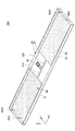
- FIG. 6 is a perspective perspective view showing an RFID tag 300 according to Embodiment 3.
- FIG. 6 is a perspective perspective view showing an RFID tag 400 according to Embodiment 4.
- FIG. 10 is a perspective perspective view showing an RFID tag 500 of a fifth embodiment.
- FIG. 10 is a perspective perspective view showing an RFID tag 600 of a sixth embodiment.
- 1A and 1B are perspective perspective views showing RFID tags 10 and 10A of Comparative Example 1, respectively.
- 1A and 1B an XYZ coordinate system (orthogonal coordinate system) is defined as illustrated.
- the RFID tag 10 of Comparative Example 1 includes a substrate 20, an antenna 30, and an IC (Integrated Circuit) chip 40.
- the substrate 20 may be an insulating substrate, and for example, a FR-4 (Flame Retardant type 4) standard substrate may be used.
- substrate 20 can use what has copper foil formed in the surface 21 and the back surface (surface on the opposite side of the surface 21), for example.
- the antenna 30 includes antenna elements 31 to 35.
- the antenna elements 31 and 32 are formed on the surface 21 of the substrate 20.
- An IC chip 40 is connected between the linear portions 31D and 32D of the antenna elements 31 and 32.
- the antenna elements 31 and 32 are formed, for example, by patterning a copper foil attached to the surface 21 of the substrate 20.
- the antenna element 33 is formed on the back surface (surface opposite to the front surface 21) of the substrate 20.
- a copper foil attached to the back surface of the substrate 20 can be used.
- the antenna element 34 is formed on the side surface of the substrate 20 on the X axis negative direction side, and the antenna element 35 is formed on the side surface of the substrate 20 on the X axis positive direction side.
- the antenna elements 34 and 35 are produced by forming a copper plating layer on the side surface of the substrate 20 by, for example, electroless plating or electrolytic plating.
- the antenna elements 31 to 35 form a loop together with the IC chip 40. That is, the antenna 30 is a loop antenna.
- the IC chip 40 is mounted on the surface 21 of the substrate 20 and is electrically connected to the antenna elements 31 and 32, and stores data representing a unique ID in an internal memory chip.
- the IC chip 40 receives a signal for reading in the RF (Radio-Frequency) band from the reader / writer of the RFID tag 10 via the antenna 30, the IC chip 40 operates with the power of the received signal, and transmits data representing the ID via the antenna 30. send. Thereby, the ID of the RFID tag 10 can be read by the reader / writer.
- RF Radio-Frequency
- the RFID tag 10 of Comparative Example 1 is assumed to be attached to the surface of a metal article, for example, the height of the antenna 30 is gained by the substrate 20 and the antenna 30 is formed in a loop shape. .
- the RFID tag 10 is attached to the surface of a metal article with the antenna element 33 on the bottom surface.
- the RFID tag 10 of the comparative example 1 has the loop-shaped antenna 30 formed around the substrate 20 having a certain height.
- the thickness of the substrate 20 can be reduced to, for example, about 5 mm.
- portions perpendicular to the surface of the metal article are generated. Therefore, when the RFID tag 10 performs communication, the current flowing in the antenna 30 is prevented by a mirror image effect. A mirror image current flows.
- the RFID tag 10 of Comparative Example 1 uses this mirror image effect to improve the radiation characteristics of the antenna 30.
- a plurality of vias 34A and 35A may be provided as in the RFID tag 10A shown in FIG. 1B.
- the antenna elements 31, 32 and the antenna element 33 are connected by ten vias 34A and ten vias 35A.
- the vias 34A and 35A form a copper plating layer by forming a through hole in the substrate 20 by, for example, drilling or laser processing, and performing an electroless plating process and an electrolytic plating process on the inner wall of the through hole. Can be produced.
- ten vias 34A and 35A are formed in order to make the characteristics of the antenna 30 substantially the same as when using the antenna elements 34 and 35 formed of a copper plating layer. This is because 34A and 35A are necessary.
- the number of vias 34A and 35A is not limited to ten and may be larger, but it is necessary to form at least the entire Y-axis direction.
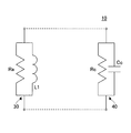
- FIG. 1C is a diagram showing an equivalent circuit of the RFID tag 10 of Comparative Example 1.
- the antenna 30 of the RFID tag 10 can be represented by a resistor Ra and an inductor L1
- the IC chip 40 of the RFID tag 10 can be represented by a resistor Rc and a capacitor Cc. That is, the antenna 30 includes a resistance component and an inductance component
- the IC chip 40 can be represented by a resistance component and a capacitance component.
- the resistor Ra is a resistor having a resistance value Ra
- the inductor L1 is an inductor having an inductance L1.
- the resistor Rc is a resistor having a resistance value Rc
- the capacitor Cc is a capacitor having a capacitance Cc.
- the equivalent circuit of the RFID tag 10A (see FIG. 1B) of Comparative Example 1 is the same as the equivalent circuit of the RFID tag 10 shown in FIG. 1C.
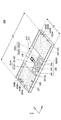
- 2A and 2B are perspective perspective views showing RFID tags 10B and 10C of Comparative Example 2, respectively.
- the same components as those of the RFID tags 10 and 10A of Comparative Example 1 are denoted by the same reference numerals, and the description thereof is omitted.
- the RFID tag 10B of Comparative Example 2 includes a substrate 20B, an antenna 30B, an IC chip 40, and a capacitor 50.
- the substrate 20B is the same substrate as the substrate 20 of Comparative Example 1, but the length in the X-axis direction is shorter than that of the substrate 20.
- the antenna 30B includes antenna elements 31B to 35B.
- the antenna elements 31B and 32B are formed on the surface 21B of the substrate 20B.
- An IC chip 40 is connected between the antenna elements 31B and 32B.
- the antenna 30 ⁇ / b> B is a loop antenna as in the antenna 30 of the first comparative example.
- the antenna elements 31B and 32B are formed, for example, by patterning a copper foil attached to the surface 21B of the substrate 20B.
- As the antenna element 33B for example, a copper foil attached to the back surface of the substrate 20B can be used as it is.
- the antenna elements 34B and 35B are formed by forming a copper plating layer on the side surface of the substrate 20B, for example, by electroless plating or electrolytic plating.
- the antenna elements 31B, 32B, and 33B of the antenna 30B are arranged in the X-axis direction. Is shorter than the antenna elements 31, 32, and 33 of the first comparative example. Note that the length (width) of the antenna elements 31B, 32B, and 33B in the Y-axis direction is the same as the width of the antenna elements 31, 32, and 33 of Comparative Example 1.
- the antenna elements 34B and 35B are the same as the antenna elements 34 and 35 of the first comparative example.
- the IC chip 40 is mounted on the surface 21B of the substrate 20B and connected between the antenna elements 31B and 32B.
- the capacitor 50 is formed on the surface 21B of the substrate 20B between the antenna elements 31B and 32B.
- the capacitor 50 includes pattern portions 51, 52, and 53 that are arranged in parallel to each other.
- the pattern part 52 extends from the extension part 31B1 of the antenna element 31B, and the pattern parts 51 and 53 extend from the extension part 32B1 of the antenna element 32B.
- the pattern units 51, 52, and 53 are arranged in parallel to each other to construct two capacitors in a plan view.
- a capacitor is also constructed in plan view between the pattern portions 51 to 53 and the extending portions 31B1 and 32B1.
- vias 34C and 35C may be included as in the RFID tag 10C shown in FIG. 2B.
- the vias 34C and 35C are the same as the vias 34A and 35A (see FIG. 1B) of the first comparative example.
- FIG. 2C is a diagram showing an equivalent circuit of the RFID tag 10B of Comparative Example 2.
- the antenna 30B of the RFID tag 10B can be represented by a resistor Ra, an inductor L2, and a capacitor Ca.
- the IC chip 40 of the RFID tag 10B can be represented by a resistor Rc and a capacitor Cc. That is, the antenna 30B includes a capacitance component corresponding to the capacitor 50 in addition to the resistance component and the inductance component.
- the capacitor 50 is treated as a capacitance component of the antenna 30B.
- the resistor Ra is a resistor having a resistance value Ra
- the inductor L2 is an inductor having an inductance L2
- the capacitor Ca is a capacitor having a capacitance Ca
- the resistor Rc is a resistor having a resistance value Rc
- the capacitor Cc is a capacitor having a capacitance Cc.
- the lengths (widths) of the antenna elements 31B, 32B, and 33B of Comparative Example 2 in the Y-axis direction are the same as those of the antenna elements 31, 32, and 33 of Comparative Example 1, but the antenna elements 31B, 32B, and 33B are the same. Is shorter than the antenna elements 31, 32, 33.
- the inductance component (L2) of the antenna 30B is smaller than the inductance component (L1) of the antenna 30. This is because the inductance is smaller for the short conductor when the conductor widths are equal.
- the resonance frequency of the RFID tag 10 shown in FIG. 1A and the resonance frequency f of the RFID tag 10B shown in FIG. 2A are obtained by the general formula (1).
- L is the inductance (L1) of the inductor L1 shown in FIG. 1C
- C is the capacitance of the capacitor Cc.
- L is the inductance (L2) of the inductor L2 shown in FIG. 2C
- C is the combined capacitance of the capacitor Ca and the capacitor Cc.
- the inductance L2 is smaller than the inductance L1. Further, since the capacitor Ca and the capacitor Cc are connected in parallel, the combined capacitance of the capacitor Ca and the capacitor Cc is larger than the capacitance of the capacitor Cc.
- the RFID tag 10B of the comparative example 2 is the same as the RFID tag 10 of the comparative example 1 by compensating for the decrease in inductance caused by including the antenna 30B smaller than the antenna 30 of the comparative example 1 by the capacitance of the capacitor 50. It is possible to obtain a resonance frequency of.
- the RFID tag 10B of the comparative example 2 includes the capacitor 50, thereby enabling the antenna 30B to be downsized. As a result, the RFID tag 10B can be downsized in the Y-axis direction.
- the RFID tag 10 of Comparative Example 1 shown in FIG. 1A has a length in the X-axis direction of 65 mm and a width in the Y-axis direction of 17 mm.
- the RFID tag 10B of Comparative Example 2 shown in FIG. 2A has a length in the X-axis direction of 45 mm and a width in the Y-axis direction of 17 mm.
- the RFID tag 10B of the comparative example 2 includes the capacitor 50, so that the length in the X-axis direction is shortened while maintaining the same use frequency as that of the RFID tag 10 of the comparative example 1. I am trying.
- the antennas 30 and 30B of the RFID tags 10 and 10B of Comparative Examples 1 and 2 have high manufacturing costs because the antenna elements 34, 34B, 35, and 35B are formed by plating.
- the antennas 30 and 30B of the RFID tags 10A and 10C of Comparative Examples 1 and 2 have high manufacturing costs because the antenna elements 34A, 34C, 35A, and 35C are constructed with vias.
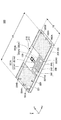
- FIG. 3A is a perspective perspective view showing the RFID tag 100 according to the first embodiment.
- an XYZ coordinate system orthogonal coordinate system
- the RFID tag 100 includes a substrate 110, an antenna 120, and an IC (Integrated Circuit) chip 130.
- the substrate 110 may be an insulating substrate, and for example, a FR-4 (Flame Retardant type 4) standard substrate may be used.
- a substrate having a copper foil formed on the front surface 111 and the back surface (the surface opposite to the front surface 111) can be used.
- a substrate 110 for example, a substrate in which a copper foil is attached to the front and back surfaces of a single insulating layer can be used.
- a prepreg can be used as the insulating layer.
- the prepreg is an insulating layer obtained by impregnating an insulating resin such as epoxy or polyimide into a woven or non-woven fabric such as glass fiber or carbon fiber.
- the insulating resin is preferably a thermosetting resin.
- the substrate 110 can be manufactured by thermocompression bonding of the copper foil and the insulating layer.
- the substrate 110 is not limited to the FR-4 standard substrate, and may be another standard substrate such as FR-5.
- the substrate 110 may be made of a resin such as polycarbonate.
- the antenna 120 includes antenna elements 121 to 123 and vias 124A, 124B, 125A, and 125B.
- the antenna elements 121 and 122 are formed on the surface 111 of the substrate 110.
- the antenna elements 121 and 122 are an example of a pair of first antenna elements.
- the antenna element 121 has an extending part 121A that extends in the X-axis positive direction
- the antenna element 122 has an extending part 122A that extends in the X-axis negative direction.
- An IC chip 130 is connected to the extending portion 121 ⁇ / b> A of the antenna element 121 and the extending portion 122 ⁇ / b> A of the antenna element 122.
- the extending portions 121A and 122A are linear portions 121A1 and 122A1 extending linearly in the X-axis direction from the antenna elements 121 and 122, respectively, and linear portions 121A2 that are bent in the Y-axis positive direction from the ends of the linear portions 121A1 and 122A1. , 122A2, and has an L-shape in plan view.
- Each of the straight portions 121A1 and 122A1 is an example of a straight connection portion.
- the straight portions 121A2 and 122A2 are not necessarily required, and may include only the straight portions 121A1 and 122A1 and have a linear shape in plan view.
- Such antenna elements 121 and 122 are formed, for example, by patterning a copper foil attached to the surface 111 of the substrate 110.
- the antenna element 123 is formed on the back surface (surface opposite to the front surface 111) of the substrate 110.
- the antenna element 123 is an example of a second antenna element.
- a copper foil attached to one surface of the back surface of the substrate 110 can be used as it is.
- the material of the antenna elements 121 to 123 is not limited to copper, and may be a metal other than copper, such as aluminum.
- the vias 124A and 124B are formed at the end of the substrate 110 on the X axis negative direction side (near the end side), and the vias 125A and 125B are the ends of the substrate 110 on the X axis positive direction side (near the end side). Formed.
- the vias 124A, 124B, 125A, 125B are formed by forming a through hole in the substrate 110 by, for example, drilling or laser processing, and performing an electroless plating process and an electrolytic plating process on the inner wall of the through hole. It can be produced by forming a layer.
- the via 124A and the via 125A have the same position in the Y-axis direction. That is, the position where the via 124A is formed between the antenna element 121 and the antenna element 123 in the Y-axis direction (the width direction of the RFID tag 100) is such that the via 125A is located between the antenna element 122 and the antenna element 123 in the Y-axis direction. It is equal to the position formed between.
- the vias 124A and 125A are arranged on the same straight line parallel to the X axis together with the straight portions 121A1 and 122A1.
- the via 124A and the via 125A are an example of a pair of first connection portions.
- the via 124B and the via 125B have the same position in the Y-axis direction. That is, the position where the via 124B is formed between the antenna element 121 and the antenna element 123 in the Y-axis direction (the width direction of the RFID tag 100) is the same as the position of the via 125B between the antenna element 122 and the antenna element 123 in the Y-axis direction. It is equal to the position formed between.
- the vias 124B and 125B are located on the Y axis positive direction side with respect to the straight line including the straight portions 121A1 and 122A1 in the Y axis direction.
- the via 124B and the via 125B are an example of a pair of second connection portions.
- the vias 124B and 125B are formed at corners of the rectangular substrate 110 in plan view.
- the corner portion where the via 124B is formed is a portion slightly inside the vertex 110A on the X axis negative direction side and the Y axis positive direction side of the substrate 110, and is in the vicinity of the vertex 110A.
- the corner where the via 125B is formed is a portion slightly inside the top 110B on the X-axis positive direction side and the Y-axis positive direction side of the substrate 110, and is in the vicinity of the top 110B.
- the vias 124B and 125B cannot be formed on the top portions 110A and 110B of the substrate 110, they are formed at corners slightly inside the top portions 110A and 110B.
- the length of the loop formed by the antenna elements 121 to 123 and the vias 124B and 125B is longer than the length of the loop formed by the antenna elements 121 to 123 and the vias 124A and 125A.
- the loop formed by the antenna elements 121 to 123 and the vias 124A and 125A is an example of the first loop
- the loop formed by the antenna elements 121 to 123 and the vias 124B and 125B is the second loop. It is an example. Forming the vias 124B and 125B at the corners of the substrate 110 is effective for increasing the length of the second loop.
- the antenna 120 including the antenna elements 121 to 123 and the vias 124A, 124B, 125A, and 125B is a loop antenna.
- the length of the antenna 120 may be set according to the frequency used for the wireless communication of the RFID tag 100.
- the effective length of the antenna 120 is a length between a point connected to the IC chip 130 of the extending part 121A and a point connected to the IC chip 130 of the extending part 121B.
- the effective length of the antenna 120 is referred to as a loop length.
- the antenna 120 shown in FIG. 3A is a loop antenna that works as an inductance, unlike a loop antenna that combines two so-called dipole antennas. For this reason, the loop length of the antenna 120 is set shorter than the wavelength ⁇ at the used frequency.
- a loop formed by the antenna elements 121 to 123 and the vias 124A and 125A, a loop formed by the antenna elements 121 to 123 and the vias 124B and 125B ( There is a second loop).
- the loop length of the antenna 120 is set to be shorter than the wavelength ⁇ at the used frequency in both the first loop and the second loop.
- the RFID tag 100 according to Embodiment 1 is different from a so-called loop antenna in which the loop length is set to a length corresponding to one wavelength, by making the loop length of the antenna 120 shorter than the length ( ⁇ ) corresponding to one wavelength.
- the antenna 120 is used as an inductance.
- the current distribution becomes non-uniform in the length direction of the loop because the loop length and the length ( ⁇ ) of one wavelength coincide. This is because in a so-called loop antenna, a standing wave is generated, the current is minimized at the end of the dipole antenna, and the current is maximized at the center of the dipole antenna.
- the current density distribution of the antenna 120 acting as an inductance becomes substantially uniform as a whole in the length direction of the antenna 120. This is because the standing wave does not occur because the length of the antenna 120 is less than the length ( ⁇ ) of one wavelength.
- the loop antenna 120 is different in length from a so-called loop antenna and has a different current distribution.
- the loop length of the antenna 120 may be shorter than the wavelength ⁇ at the use frequency.
- the loop length of the antenna 120 affects the impedance matching between the loop antenna 120 and the IC chip 130.
- the resistance component and the capacitor component of the IC chip 130 also affect.
- the length of the antenna 120 is, for example, 1/3 ( ⁇ / 3) or less of the wavelength ⁇ at the operating frequency. It is preferable to set to. When such a loop length is set, it is possible to match the impedances of the antenna 120 serving as an inductance and the resistance component and capacitor component of the IC chip 130.
- the current density distribution of the antenna 120 becomes substantially uniform as a whole in the length direction of the antenna 120.
- the length of the loop antenna 120 acting as an inductance is set so that the impedances of the loop antenna 120 and the resistance component and capacitor component of the IC chip 130 are matched.
- the loop length of the antenna 120 of the RFID tag 100 of Embodiment 1 is determined by the size of the substrate 110 that holds the antenna 120 and the dielectric constant of the substrate 110.
- the loop length of the antenna 120 may be set according to the frequency used. Further, since 915 MHz is assigned as a typical frequency in the United States and 868 MHz is assigned as a representative frequency in Europe (EU), the loop length of the antenna 120 may be set in accordance with these frequencies.
- the resonance frequency of the RFID tag 100 of Embodiment 1 is 953 MHz.
- the IC chip 130 is mounted on the surface 111 of the substrate 110 and is electrically connected to the antenna elements 121 and 122, and stores data representing a unique ID in an internal memory chip.
- the IC chip 130 receives a signal for reading in the RF (Radio-Frequency) band from the reader / writer of the RFID tag 100 via the antenna 120, the IC chip 130 operates with the power of the received signal, and transmits data representing the ID via the antenna 120. send. Thereby, the ID of the RFID tag 100 can be read by the reader / writer.
- RF Radio-Frequency
- FIG. 3B is a diagram illustrating an equivalent circuit of the RFID tag 100 according to the first embodiment.
- the antenna 120 of the RFID tag 100 can be represented by a resistor Ra and inductors La1 and La2, and the IC chip 130 of the RFID tag 100 can be represented by a resistor Rc and a capacitor Cc.
- the resistor Ra is a resistor having a resistance value Ra
- the inductor La1 is an inductor having an inductance La1
- the inductor La2 is an inductor having an inductance La2.
- the inductance La1 is handled as the inductance of the first loop of the antenna 120
- the inductance La2 is handled as the inductance of the second loop of the antenna 120.
- the resistor Rc is a resistor having a resistance value Rc
- the capacitor Cc is a capacitor having a capacitance Cc.
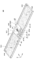
- FIG. 4 is a perspective perspective view showing an RFID tag 10D in which the number of vias 34A and 35A of the RFID tag 10A of Comparative Example 1 is reduced to two.
- the antenna 30 of the RFID tag 10D shown in FIG. 4 includes vias 34A1, 34A2, 35A1, and 35A2.
- the vias 34A1, 34A2, 35A1, and 35A2 are obtained by reducing the ten vias 34A and 35A of the RFID tag 10A of Comparative Example 1 to two.
- the vias 34A1, 34A2, 35A1, and 35A2 have the same positions in the Y-axis direction as the vias 124A, 124B, 125A, and 125B of the RFID tag 100 of the first embodiment.
- the vias 34A1 and 35A1 are formed so as to be positioned on the same straight line as the straight portions 31D and 32D of the antenna elements 31 and 32.
- the vias 34A2 and 35A2 are formed on the Y axis positive direction side with respect to the straight line including the straight portions 31D and 32D.
- the loop including the antenna elements 31, 32, 33 and the vias 34A1, 35A1 is referred to as a first loop
- the loop including the antenna elements 31, 32, 33 and the vias 34A2, 35A2 is referred to as a second loop.
- the length of the second loop is longer than that of the first loop.
- the inductance of the antenna 30 of the RFID tag 10D is larger than the inductance of the antenna 30 of the RFID tag 10A. This is because the number of vias has decreased. If the length is the same, the smaller the conductor is, the larger the inductance is. If the width is the same, the longer the inductance is, the larger the inductance is.
- the inductances of the first loop and the second loop of the antenna 30 of the RFID tag 10D shown in FIG. 4 are La1A and La2A, respectively. Further, the inductance of the antenna 30 of the RFID tag 10A shown in FIG. 1B is L1.
- La2A> La1A> L1 is established between the inductances La1A, La2A, and L1. This is because La2A> La1A is established because the second loop is longer than the first loop, and the number of vias is reduced, so that the antenna 30 of the RFID tag 10D shown in FIG. This is because La1A> L1 is established with the antenna 30 of the RFID tag 10A shown.
- the inductance of the antenna 30 increases, and the resonance frequency expressed by the equation (1) Decreases and resonance occurs at a frequency lower than 953 MHz.
- the loop length of the antenna 120 is shortened and the antenna The inductance of 120 needs to be smaller than the inductance of the antenna 30 of the RFID tag 10A of Comparative Example 1.
- the length in the X-axis direction is 65 mm
- the width in the Y-axis direction is 17 mm.
- the length X1 in the X-axis direction of the RFID tag 100 of Embodiment 1 can be 55 mm, and the width Y1 in the Y-axis direction can be 17 mm.
- FIG. 5 is a diagram illustrating a first loop and a second loop of the RFID tag 100 according to the first embodiment.
- the admittance Yin of the antenna 120 can be expressed by Equation (2). it can.
- Equation (2) since La2> La1, it can be seen from Equation (2) that the admittance Yin of the antenna 120 is more affected by the inductance La1 of the first loop than the inductance La2 of the second loop.
- the resonance frequency of the RFID tag 100 of Embodiment 1 is 953 MHz, and the wavelength ⁇ at 953 MHz is about 300 mm. Since the length of the antenna 120 is shorter than one wavelength, the second loop having a long loop length is used. It is considered that the gain is higher than that of the first loop. This is because the length of the second loop is closer to the length of one wavelength than the length of the first loop.
- the first loop mainly works to determine the resonance frequency f of the antenna 120 (that is, to obtain impedance matching), and the second loop mainly works to determine the gain of the antenna 120. .
- the antenna 120 when the antenna 120 is viewed as a whole, the antenna 120 has inductance due to the combined loop of the first loop and the second loop, but the roles of the first loop and the second loop are different due to the above-described tendency. Can be considered.
- the vias 124A, 124B, and 125A are mainly determined so that the resonance frequency is determined by the vias 124A and 125A included in the first loop and the gain of the antenna 120 is determined by the vias 124B and 125B included in the second loop. , 125B may be determined.
- the antenna 120 is constructed using the vias 124A and 125A that are an example of a pair of first vias and the vias 124B and 125B that are an example of a pair of second vias.
- the cost can be reduced by reducing the number of vias.
- antenna elements 34 and 35 are formed on the entire side surfaces in the X-axis direction of the substrates 20 and 20B by plating.
- the RFID tag 100 of the first embodiment only forms two pairs of vias 124A, 124B, 125A, and 125B, so that the cost can be reduced.
- the RFID tags 10A (see FIG. 1B) and 10C (see FIG. 2B) of Comparative Examples 1 and 2 include 10 vias 34A and 35A along the entire side surface in the X-axis direction of the substrates 20 and 20B. 34C and 35C are formed.
- the RFID tag 100 of the first embodiment only forms two pairs of vias 124A, 124B, 125A, and 125B, so that the cost can be reduced.
- the RFID tag 100 (see FIG. 5) according to the first embodiment can achieve downsizing of the RFID tag 100 as compared with the comparative RFID tag 10D shown in FIG.
- the RFID tag 100 according to Embodiment 1 can have the length X1 in the X-axis direction of 55 mm. This is a value about 20% smaller than the length (65 mm) in the X-axis direction of the comparative RFID tag 10D shown in FIG. That is, a reduction in size of about 20% can be achieved, and a reduction in weight can be achieved thereby.
- the cost reduction can be achieved by downsizing the RFID tag 100 as described above.
- the RFID tag 100 can reduce the material cost by the amount that the substrate 110 and the antenna 120 can be reduced by about 20%, thereby achieving cost reduction.
- the RFID tag 100 according to Embodiment 1 includes a loop antenna 120.
- the reason for including such a loop-shaped antenna 120 is to enable communication even when the RFID tag 100 is attached to the surface of a metal article.
- an RFID tag including a loop antenna has a higher manufacturing cost than a very thin RFID tag in which a dipole antenna and an IC chip are mounted on the surface of a thin sheet substrate.
- the RFID tag 100 including the loop-shaped antenna 120 and reducing the cost.
- an RFID tag including a loop antenna tends to be larger and heavier than a very thin RFID tag in which a dipole antenna and an IC chip are mounted on the surface of a thin sheet substrate.
- the RFID tag 100 that includes the loop-shaped antenna 120 and is reduced in size and weight.
- the RFID tag 100 includes vias 124B and 125B formed at positions offset in the Y-axis direction with respect to the linear portions 121A1 and 121A1 of the antenna 120. Vias 124B and 125B form a second loop.
- Such a second loop has substantially the same length as the loops of the antennas 30 and 30B of the RFID tags 10, 10A, 10B, and 10C of Comparative Examples 1 and 2. This is because the vias 124B and 125B included in the second loop are offset in the Y-axis direction with respect to the straight portions 121A1 and 121A1.
- the RFID tag 100 of Embodiment 1 can obtain substantially the same gain as the RFID tags 10, 10A, 10B, and 10C of Comparative Examples 1 and 2.
- the RFID tag 100 even if the RFID tag 100 according to the first embodiment is attached to the surface of a metal article, the RFID tag 100 has substantially the same communication distance as the RFID tags 10, 10A, 10B, and 10C of Comparative Examples 1 and 2.
- the vias 124A and 125A are arranged on the same straight line parallel to the X axis together with the straight portions 121A1 and 122A1.
- the Q value of the antenna 120 can be lowered and the band of the antenna 120 is widened.
- the RFID tag 100 forms two loops (first loop and second loop) in the antenna 120 using two pairs of vias 124A, 124B, 125A, and 125B. Cost reduction is planned. Also, cost reduction is achieved by downsizing. The conventional RFID tag has not been sufficiently reduced in cost.
- the RFID tag 100 can perform communication even when attached to the surface of a metal article.
- the vias 124A and 125A are arranged on the same straight line parallel to the X axis together with the straight portions 121A1 and 122A1, and the vias 124B and 125B are more in the Y axis direction than the straight line including the straight portions 121A1 and 122A1.
- the form located on the Y axis positive direction side has been described. Accordingly, the second loop including the vias 124B and 125B is made longer than the first loop including the vias 124A and 125A.
- the vias 124A and 125A together with the straight portions 121A1 and 122A1 are on the same straight line parallel to the X axis. It does not need to be arranged.
- the vias 124A and 125A are not positioned on the straight line including the straight portions 121A1 and 122A1, It may be formed at a position shifted in the Y-axis direction.
- FIG. 6A is a perspective perspective view showing the RFID tag 200 of the second embodiment.
- an XYZ coordinate system orthogonal coordinate system
- the same components as those of the RFID tag 100 of Embodiment 1 are denoted by the same reference numerals, and the description thereof is omitted.
- the RFID tag 200 of the second embodiment includes a substrate 210, an antenna 220, an IC chip 130, and a capacitor 240.
- the length X2 in the X-axis direction is shorter than the length X1 (see FIG. 3A) of the RFID tag 100 according to the first embodiment.
- the length X2 is 45 mm as an example. That is, this is the same length as the RFID tag 10B of Comparative Example 2 (see FIG. 2A).
- the length Y2 in the Y-axis direction of the RFID tag 200 of the second embodiment is the same (17 mm) as the length Y1 (see FIG. 3A) of the RFID tag 100 of the first embodiment in the Y-axis direction.
- the substrate 210 may be an insulating substrate like the substrate 110 of the first embodiment, and for example, an FR-4 standard substrate can be used.
- a substrate having a copper foil formed on the front surface 211 and the back surface (the surface opposite to the front surface 211) can be used.
- the length of the substrate 210 in the X-axis direction is equal to the X of the substrate 110 of the first embodiment. It is shorter than the axial length.
- the antenna 220 includes antenna elements 221 to 223 and vias 224A, 224B, 225A, and 225B.
- the antenna elements 221 and 222 are formed on the surface 211 of the substrate 210.
- the antenna elements 221 and 222 are an example of a pair of first antenna elements.
- the antenna element 221 has an extending part 221A that extends in the X-axis positive direction
- the antenna element 222 has an extending part 222A that extends in the X-axis negative direction.
- the IC chip 130 is connected to the extending portion 221 ⁇ / b> A of the antenna element 221 and the extending portion 222 ⁇ / b> A of the antenna element 222.
- the extending portions 221A and 222A are respectively linear portions 221A1 and 222A1 that extend linearly from the antenna elements 221 and 222 in the X-axis direction, and linear portions 221A2 that are bent in the Y-axis positive direction from the ends of the linear portions 221A1 and 222A1.
- 222A2 and has an L shape in plan view.
- the straight portions 221A1 and 222A1 are examples of straight connection portions, respectively.
- the antenna element 223 is formed on the back surface of the substrate 210 (surface opposite to the front surface 211).
- the antenna element 223 is an example of a second antenna element.
- the lengths of the antenna elements 221, 222, and 223 in the X-axis direction are respectively The antenna elements 121, 122, 123 of Embodiment 1 are shorter than the length in the X-axis direction.
- the vias 224A and 224B are formed at the end of the substrate 210 on the X axis negative direction side (near the end side), and the vias 225A and 225B are the ends of the substrate 210 on the X axis positive direction side (near the end side). Formed.
- the via 224A and the via 225A have the same position in the Y-axis direction. That is, the position where the via 224A is formed between the antenna element 221 and the antenna element 223 in the Y-axis direction (the width direction of the RFID tag 200) is such that the via 225A is located between the antenna element 222 and the antenna element 223 in the Y-axis direction. It is equal to the position formed between.
- the vias 224A and 225A are arranged on the same straight line parallel to the X axis together with the straight portions 221A1 and 222A1.
- the via 224A and the via 225A are an example of a pair of first connection portions.
- the via 224B and the via 225B have the same position in the Y-axis direction. That is, the position where the via 224B is formed between the antenna element 221 and the antenna element 223 in the Y-axis direction (the width direction of the RFID tag 200) is such that the via 225B is located between the antenna element 222 and the antenna element 223 in the Y-axis direction. It is equal to the position formed between.
- the vias 224B and 225B are located on the Y axis positive direction side with respect to the straight line including the straight portions 221A1 and 222A1 in the Y axis direction.
- the via 224B and the via 225B are an example of a pair of second connection portions.
- the length of the second loop formed by the antenna elements 221 to 223 and the vias 224B and 225B is longer than the length of the first loop formed by the antenna elements 221 to 223 and the vias 224A and 225A. .
- the antenna 220 including such antenna elements 221 to 223 and vias 224A, 224B, 225A, 225B is a loop antenna.
- the length of the antenna 220 may be set according to the frequency used for the wireless communication of the RFID tag 200.
- the effective length of the antenna 220 is a length between a point connected to the IC chip 130 of the extending part 221A and a point connected to the IC chip 130 of the extending part 221B.
- the resonance frequency of the RFID tag 200 of Embodiment 2 is 953 MHz.
- FIG. 6B is an enlarged view showing the capacitor 240 of the RFID tag 200 of Embodiment 2
- FIG. 6C is an enlarged view of the capacitor 50 of the RFID tag 10B of Comparative Example 2.
- the IC chip 130 is omitted.
- the capacitor 240 is formed on the surface 211 of the substrate 210 between the antenna elements 221 and 222.
- the capacitor 240 has pattern portions 241, 242, and 243 arranged in parallel to each other.
- the pattern portion 242 extends from a branch portion 221A3 that branches from the straight portion 221A1 of the antenna element 221, and the pattern portions 241 and 243 extend from a branch portion 222A3 that branches from the straight portion 222A1 of the antenna element 222. Yes.
- the pattern parts 241, 242, and 243 are arranged in parallel to each other to construct two capacitors in a plan view.
- a capacitor is also constructed between the pattern portions 241 to 243 and the straight portions 221A1 and 222A1 in plan view.
- Such a capacitor 240 is formed simultaneously with the antenna 220 by, for example, patterning a copper foil attached to the surface 211 of the substrate 210.
- the width of the pattern portions 241, 242, and 243 in the Y-axis direction is the pattern portion 51 of the capacitor 50.
- 52 and 53 are narrower than the width in the Y-axis direction.
- the lengths in the X-axis direction of the pattern portions 241, 242, and 243 and the pattern portions 241, 242, and 243 are the same.
- the interval between the Y-axis directions of the pattern portions 241, 242, and 243 is wider than the interval between the Y-axis directions of the pattern portions 51, 52, and 53.
- the capacitance of the capacitor 240 of the second embodiment is smaller than the capacitance of the capacitor 50 of the comparative example 2. This is because the distance between the electrodes of the capacitor 240 is longer than the distance between the electrodes of the capacitor 50 of Comparative Example 2.
- the antenna 220 of the RFID tag 200 of the second embodiment forms two pairs of vias 224A, 224B, 225A, and 225B, so that the RFID tag 10B of the comparative example 2 (like the RFID tag 100 of the first embodiment) ( The inductance is larger than that of the antenna 20B of FIG. 2A).
- the antenna 220 In order to maintain the same resonance frequency as the RFID tag 10B of the comparative example 2 (see FIG. 2A) using the antenna 220 having a large inductance in this way, the antenna is formed by forming the vias 224A, 224B, 225A, and 225B.
- the increase in inductance of 220 needs to be offset by reducing the capacitance of capacitor 240.
- the RFID tag 200 of the second embodiment maintains the same resonance frequency while maintaining the same length in the X-axis direction as the RFID tag 10B of the second comparative example (see FIG. 2A). .
- the IC chip 130 is mounted on the surface 211 of the substrate 210 and is electrically connected to the antenna elements 221 and 222, and stores data representing a unique ID in an internal memory chip.
- the IC chip 130 receives a signal for reading in an RF (Radio-Frequency) band from the reader / writer of the RFID tag 200 via the antenna 220, the IC chip 130 operates with the power of the received signal, and transmits data representing the ID via the antenna 220. send. Thereby, the ID of the RFID tag 200 can be read by the reader / writer.
- RF Radio-Frequency
- FIG. 7A is a diagram showing an equivalent circuit of the RFID tag 200 of the second embodiment.
- the antenna 220 of the RFID tag 200 can be represented by a resistor Ra, an inductor La11, an inductor La21, and a capacitor Ca1, and the IC chip 130 of the RFID tag 200 is composed of a resistor Rc and a capacitor Cc.
- Inductor La11 and inductor La21 represent inductance components of the first loop and the second loop, respectively.
- the antenna 220 includes a capacitance component corresponding to the capacitor 240 in addition to the resistance component and the inductance component.
- the capacitor 240 is treated as the capacitance component of the antenna 220.
- the resistor Ra is a resistor having a resistance value Ra
- the inductor La11 is an inductor having an inductance La11.
- the inductor La21 is an inductor having an inductance La21
- the capacitor Ca1 is a capacitor having a capacitance Ca1. Note that La21> La11.
- the resistor Rc is a resistor having a resistance value Rc
- the capacitor Cc is a capacitor having a capacitance Cc.
- the capacitance of the capacitor Ca1 is smaller than the capacitor Ca of the comparative example 2. That is, Ca> Ca1 is established.
- the inductance (the combined inductance of La11 and La21) of the antenna 220 of the RFID tag 200 of Embodiment 2 is larger than the inductance L2 (see FIG. 2C) of the antenna 20B of Comparative Example 2. This is because the antenna elements 221, 222, and 223 are connected by two pairs of vias 224A, 224B, 225A, and 225B.
- the capacitance of the capacitor Ca1 should be made smaller than that of the capacitor Ca of the comparative example 2.
- the capacitance of the capacitor 240 is made smaller than that of the capacitor 50 of Comparative Example 2.
- FIG. 7B is a diagram illustrating a first loop and a second loop of the RFID tag 200 according to the second embodiment.
- the admittance of the antenna 220 is more influenced by the inductance La11 of the first loop than the inductance La21 of the second loop, as in the first embodiment.
- the resonance frequency of the RFID tag 200 of the second embodiment is 953 MHz, and the wavelength ⁇ at 953 MHz is about 300 mm. Since the length of the antenna 220 is shorter than one wavelength, the second loop having a long loop length is used. It is considered that the gain is higher than that of the first loop. This is because the length of the second loop is closer to the length of one wavelength than the length of the first loop.
- the first loop mainly works to determine the resonance frequency f of the antenna 220 (that is, to obtain impedance matching), and the second loop mainly works to determine the gain of the antenna 220. .
- the antenna 220 when the antenna 220 is viewed as a whole, the antenna 220 has inductance due to the combined loop of the first loop and the second loop, but the roles of the first loop and the second loop are different due to the above-described tendency. Can be considered.
- the vias 224A, 224B, and 225A are mainly determined so that the resonance frequency is determined by the vias 224A and 225A included in the first loop and the gain of the antenna 220 is determined by the vias 224B and 225B included in the second loop.
- the position of 225B may be determined.
- the increase in the inductance of the antenna 220 due to the formation of the vias 224A, 224B, 225A, 225B is adjusted by the capacitance of the capacitor 240.
- the manufacturing tolerance of the pattern portions 241 to 243 is made larger than that of the capacitor 50 of the comparative example 2, thereby reducing the cost of the etching process.
- the second embodiment it is possible to reduce the cost by increasing the manufacturing tolerance of the capacitor 240 while increasing the inductance of the antenna 220 due to the formation of the vias 224A, 224B, 225A, and 225B.
- the illustrated RFID tag 200 can be provided.
- FIG. 8A is a perspective perspective view showing the RFID tag 300 according to the third embodiment.
- the third embodiment is a modification of the second embodiment.
- the same components as those of the RFID tag 200 (see FIG. 6A) of Embodiment 2 are denoted by the same reference numerals, and the description thereof is omitted.
- the RFID tag 300 according to the third embodiment is configured such that, instead of the vias 224A, 224B, 225A, 225B of the RFID tag 200 according to the second embodiment, the connection portions 324A, 324B, 325A and 325B are formed.
- connection portions 324A, 324B, 325A, and 325B are formed instead of the vias 224A, 224B, 225A, and 225B, the inductance of the antenna 220 is increased as compared with the comparative example 2, and thus the manufacturing tolerance is increased.
- the resonance frequency can be adjusted by the capacitor 240.
- connection portions 324A, 324B, 325A, and 325B of the RFID tag 300 of Embodiment 3 have a smaller plating area than the antenna elements 34B and 35B of the RFID tag 10B of Comparative Example 2, the cost can be reduced. Can be planned.
- FIG. 8B is a perspective perspective view showing the RFID tag 400 of the fourth embodiment.
- the fourth embodiment is a modification of the second embodiment.
- the same components as those of the RFID tag 200 of Embodiment 2 are denoted by the same reference numerals, and the description thereof is omitted.
- An RFID tag 400 according to the fourth embodiment is formed by forming vias 224B and vias 403B and vias 402B and 404B on the Y axis positive direction side of the via 224B and via 225B of the RFID tag 200 according to the second embodiment, respectively. It is.
- Vias 401B, 402B, 403B, and 404B are examples of the second connecting portion together with the vias 224B and 225B. That is, the fourth embodiment includes a plurality of pairs of second connection portions. Vias 224B, 225B, 401B, 402B, 403B, 404B, which are a plurality of pairs of second connection portions, are arranged in the short side direction (Y-axis direction) of the substrate 210.
- the vias 401B and 403B and the vias 402B and 404B are formed in the vicinity of the vias 224B and 225B, respectively, it may be considered that the second loop is formed together with the vias 224B and 225B.
- the second loop is a loop that mainly determines the gain of the RFID tag 400
- the gain of the antenna 220 can be increased by increasing the number of vias as compared to the second embodiment.
- FIG. 9A is a perspective perspective view showing the RFID tag 500 of the fifth embodiment.
- the fifth embodiment is a modification of the second embodiment.
- the same components as those of the RFID tag 200 (see FIG. 6A) of the second embodiment are denoted by the same reference numerals, and the description thereof is omitted.
- the RFID tag 500 according to the fifth embodiment is formed by forming a via 501A and a via 502A on the Y axis negative direction side of the via 224A and the via 224B of the RFID tag 200 according to the second embodiment, respectively.
- the vias 501A and 502A form a third loop different from the first loop and the second loop.
- the third loop Since the position in the Y-axis direction is shifted from the straight line portions 221A1 and 222A1, the third loop contributes to an increase in the gain of the antenna 220 as in the second loop.
- vias 501A and 502A may be added to vias 224A, 224B, 225A, and 225B.
- FIG. 9B is a perspective perspective view showing the RFID tag 600 according to the sixth embodiment.
- the sixth embodiment is a modification of the second embodiment.
- the same components as those of the RFID tag 200 (see FIG. 6A) of Embodiment 2 are denoted by the same reference numerals, and the description thereof is omitted.
- the RFID tag 600 of the sixth embodiment is an enlargement of the RFID tag 200 of the second embodiment.
- the positions of the vias 601A and 602A are the same as the vias 224A and 225A of the second embodiment, respectively.
- the RFID tag 600 of the sixth embodiment has a configuration in which the components other than the vias 224A and 225A are enlarged without changing the positions of the vias 224A and 225A in the RFID tag 200 of the second embodiment.
- the vias 601A and 602A correspond to the vias 224A and 225A of the second embodiment.
- the RFID tag 600 according to the sixth embodiment is suitable for applications in which no problem occurs even if the whole is enlarged.
- the number of vias is the same as that of the second embodiment, and the number of vias is significantly smaller than that of the RFID tag 10C of the comparative example 2. Therefore, the cost can be reduced.
- RFID tag 110 Substrate 120 Antenna 121, 122, 123 Antenna element 124A, 124B, 125A, 125B Via 130 IC chip 200 RFID tag 210 Substrate 220 Antenna 240 Capacitor 221, 222, 223 Antenna element 224A, 224B, 225A, 225B Via 241 242 243 Pattern part 300 RFID tag 324A, 324B, 325A, 325B Connection part 400 RFID tag 401B, 402B, 403B, 404B Via 500 RFID tag 501A, 502A Via 600 RFID tag 601A, 602A Via
Landscapes
- Engineering & Computer Science (AREA)
- Microelectronics & Electronic Packaging (AREA)
- Computer Hardware Design (AREA)
- Physics & Mathematics (AREA)
- General Physics & Mathematics (AREA)
- Theoretical Computer Science (AREA)
- Computer Networks & Wireless Communication (AREA)
- Details Of Aerials (AREA)
- Support Of Aerials (AREA)
Abstract
Description
図1A及び図1Bは、それぞれ、比較例1のRFIDタグ10及び10Aを示す斜視透視図である。図1A及び図1Bでは図示するようにXYZ座標系(直交座標系)を定義する。 <Comparative Example 1>
1A and 1B are perspective perspective views showing
図2A及び図2Bは、それぞれ、比較例2のRFIDタグ10B及び10Cを示す斜視透視図である。以下、比較例1のRFIDタグ10及び10Aと同様の構成要素には同一符号を付し、その説明を省略する。 <Comparative example 2>
2A and 2B are perspective perspective views showing
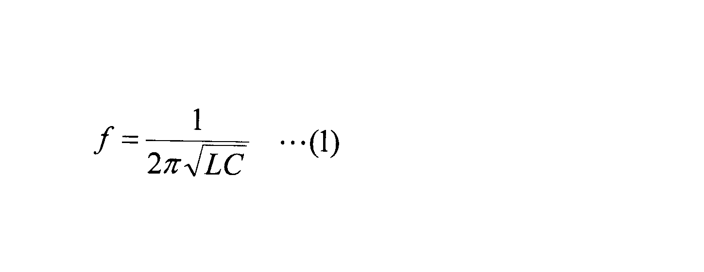
図3Aは、実施の形態1のRFIDタグ100を示す斜視透視図である。図3Aでは、比較例1、2と同様に、図示するようにXYZ座標系(直交座標系)を定義する。 <
FIG. 3A is a perspective perspective view showing the
アンテナ120の第1ループのインダクタンスLa1、第2ループのインダクタンスLa2、アンテナ120の抵抗値Ra、及び使用周波数における角周波数ωを用いると、アンテナ120のアドミタンスYinは、式(2)で表すことができる。 FIG. 5 is a diagram illustrating a first loop and a second loop of the
Using the inductance La1 of the first loop of the
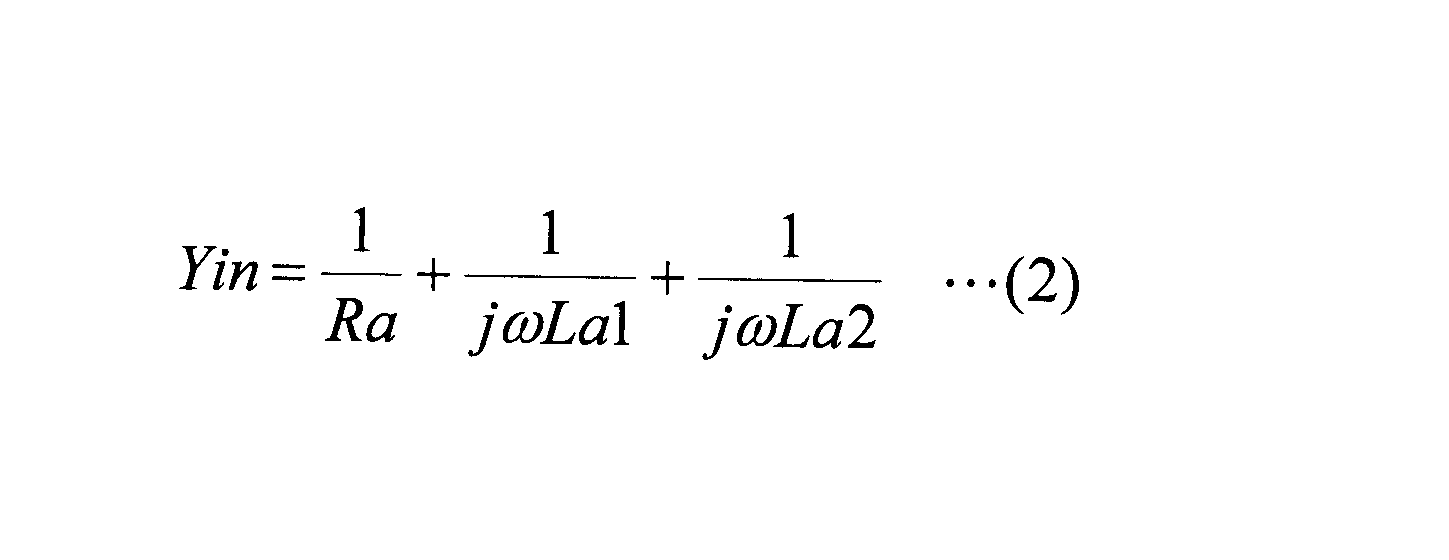
図6Aは、実施の形態2のRFIDタグ200を示す斜視透視図である。図6Aでは、実施の形態1と同様に、図示するようにXYZ座標系(直交座標系)を定義する。また、以下では、実施の形態1のRFIDタグ100の構成要素と同様の構成要素には同一符号を付し、その説明を省略する。 <Embodiment 2>
FIG. 6A is a perspective perspective view showing the
図8Aは、実施の形態3のRFIDタグ300を示す斜視透視図である。実施の形態3は、実施の形態2の変形例である。図8Aにおいて、実施の形態2のRFIDタグ200(図6A参照)と同様の構成要素には同一符号を付し、その説明を省略する。 <Embodiment 3>
FIG. 8A is a perspective perspective view showing the
図8Bは、実施の形態4のRFIDタグ400を示す斜視透視図である。実施の形態4は、実施の形態2の変形例である。図8Bにおいて、実施の形態2のRFIDタグ200(図6A参照)と同様の構成要素には同一符号を付し、その説明を省略する。 <Embodiment 4>
FIG. 8B is a perspective perspective view showing the
図9Aは、実施の形態5のRFIDタグ500を示す斜視透視図である。実施の形態5は、実施の形態2の変形例である。図9Aにおいて、実施の形態2のRFIDタグ200(図6A参照)と同様の構成要素には同一符号を付し、その説明を省略する。 <Embodiment 5>
FIG. 9A is a perspective perspective view showing the
図9Bは、実施の形態6のRFIDタグ600を示す斜視透視図である。実施の形態6は、実施の形態2の変形例である。図9Bにおいて、実施の形態2のRFIDタグ200(図6A参照)と同様の構成要素には同一符号を付し、その説明を省略する。 <Embodiment 6>
FIG. 9B is a perspective perspective view showing the
110 基板
120 アンテナ
121、122、123 アンテナエレメント
124A、124B、125A、125B ビア
130 ICチップ
200 RFIDタグ
210 基板
220 アンテナ
240 キャパシタ
221、222、223 アンテナエレメント
224A、224B、225A、225B ビア
241、242、243 パターン部
300 RFIDタグ
324A、324B、325A、325B 接続部
400 RFIDタグ
401B、402B、403B、404B ビア
500 RFIDタグ
501A、502A ビア
600 RFIDタグ
601A、602A ビア 100
Claims (10)
- 基板と、
前記基板の一方の面に形成される一対の第1アンテナエレメントと、
前記一対の第1アンテナエレメントの間に接続されるICチップと、
前記基板の他方の面に形成される第2アンテナエレメントと、
前記一対の第1アンテナエレメントと前記第2アンテナエレメントとの間に形成され、前記一対の第1アンテナエレメント、前記ICチップ、及び前記第2アンテナエレメントと第1ループを形成する一対の第1接続部と、
前記一対の第1アンテナエレメントと前記第2アンテナエレメントとの間に形成され、前記一対の第1アンテナエレメント、前記ICチップ、及び前記第2アンテナエレメントと前記第1ループよりも長い第2ループを形成する一対の第2接続部と
を含み、
前記第1ループ及び前記第2ループの長さは、それぞれ、使用周波数における波長よりも短い、RFIDタグ。 A substrate,
A pair of first antenna elements formed on one surface of the substrate;
An IC chip connected between the pair of first antenna elements;
A second antenna element formed on the other surface of the substrate;
A pair of first connections formed between the pair of first antenna elements and the second antenna element and forming a first loop with the pair of first antenna elements, the IC chip, and the second antenna element. And
The pair of first antenna elements and the second antenna element are formed between the pair of first antenna elements, the IC chip, and the second antenna element and a second loop longer than the first loop. A pair of second connecting portions to be formed,
Each of the lengths of the first loop and the second loop is an RFID tag shorter than a wavelength at a use frequency. - 前記一対の第1アンテナエレメントは、それぞれ、前記ICチップの端子と接続される直線状の接続部を有し、前記一対の接続部と、前記一対の第1接続部は、一直線上に配列される、請求項1記載のRFIDタグ。 Each of the pair of first antenna elements has a linear connection portion connected to a terminal of the IC chip, and the pair of connection portions and the pair of first connection portions are arranged on a straight line. The RFID tag according to claim 1.
- 前記基板は平面視で矩形状であり、
前記一対の第2接続部は、それぞれ、平面視で前記基板の角部に形成される、請求項1又は2記載のRFIDタグ。 The substrate is rectangular in plan view,
3. The RFID tag according to claim 1, wherein each of the pair of second connection portions is formed at a corner portion of the substrate in a plan view. - 前記一対の第1アンテナエレメントに並列に接続されるキャパシタをさらに含む、請求項1乃至3のいずれか一項記載のRFIDタグ。 The RFID tag according to any one of claims 1 to 3, further comprising a capacitor connected in parallel to the pair of first antenna elements.
- 前記キャパシタは、前記第1アンテナエレメントと同一の導電層をパターニングすることによって形成される、請求項4記載のRFIDタグ。 The RFID tag according to claim 4, wherein the capacitor is formed by patterning the same conductive layer as the first antenna element.
- 前記第2接続部を複数対含む、請求項1乃至4のいずれか一項記載のRFIDタグ。 The RFID tag according to any one of claims 1 to 4, comprising a plurality of pairs of the second connection portions.
- 前記基板は平面視で矩形状であるとともに、前記一対の第1アンテナエレメントは、前記基板の前記一方の面に、前記基板の長手方向に配列されており、
前記複数対の第2接続部は、前記基板の短手方向に配列される、請求項6記載のRFIDタグ。 The substrate is rectangular in plan view, and the pair of first antenna elements are arranged in the longitudinal direction of the substrate on the one surface of the substrate,
The RFID tag according to claim 6, wherein the plurality of pairs of second connection portions are arranged in a short direction of the substrate. - 前記第1接続部及び前記第2接続部は、前記基板を厚さ方向に貫通する貫通孔に形成されるビアである、請求項1乃至7のいずれか一項記載のRFIDタグ。 The RFID tag according to any one of claims 1 to 7, wherein the first connection portion and the second connection portion are vias formed in a through-hole penetrating the substrate in a thickness direction.
- 前記第1接続部及び前記第2接続部は、前記基板の側面に形成される、請求項1乃至7のいずれか一項記載のRFIDタグ。 The RFID tag according to any one of claims 1 to 7, wherein the first connection portion and the second connection portion are formed on a side surface of the substrate.
- 前記第1ループ及び前記第2ループの長さは、それぞれ、使用周波数における波長の1/3以下の長さに設定される、請求項1乃至9のいずれか一項記載のRFIDタグ。 The RFID tag according to any one of claims 1 to 9, wherein the lengths of the first loop and the second loop are each set to a length of 1/3 or less of a wavelength at a use frequency.
Priority Applications (5)
| Application Number | Priority Date | Filing Date | Title |
|---|---|---|---|
| PCT/JP2012/058733 WO2013145311A1 (en) | 2012-03-30 | 2012-03-30 | Rfid tag |
| JP2014507286A JP5867591B2 (en) | 2012-03-30 | 2012-03-30 | RFID tag |
| EP12873036.3A EP2833477A4 (en) | 2012-03-30 | 2012-03-30 | Rfid tag |
| CN201280070854.6A CN104160554B (en) | 2012-03-30 | 2012-03-30 | RFID label tag |
| US14/465,468 US20140361089A1 (en) | 2012-03-30 | 2014-08-21 | Rfid tag |
Applications Claiming Priority (1)
| Application Number | Priority Date | Filing Date | Title |
|---|---|---|---|
| PCT/JP2012/058733 WO2013145311A1 (en) | 2012-03-30 | 2012-03-30 | Rfid tag |
Related Child Applications (1)
| Application Number | Title | Priority Date | Filing Date |
|---|---|---|---|
| US14/465,468 Continuation US20140361089A1 (en) | 2012-03-30 | 2014-08-21 | Rfid tag |
Publications (1)
| Publication Number | Publication Date |
|---|---|
| WO2013145311A1 true WO2013145311A1 (en) | 2013-10-03 |
Family
ID=49258673
Family Applications (1)
| Application Number | Title | Priority Date | Filing Date |
|---|---|---|---|
| PCT/JP2012/058733 WO2013145311A1 (en) | 2012-03-30 | 2012-03-30 | Rfid tag |
Country Status (5)
| Country | Link |
|---|---|
| US (1) | US20140361089A1 (en) |
| EP (1) | EP2833477A4 (en) |
| JP (1) | JP5867591B2 (en) |
| CN (1) | CN104160554B (en) |
| WO (1) | WO2013145311A1 (en) |
Cited By (2)
| Publication number | Priority date | Publication date | Assignee | Title |
|---|---|---|---|---|
| WO2018092583A1 (en) * | 2016-11-15 | 2018-05-24 | 株式会社村田製作所 | Uhf-band rfid tag and uhf-band rfid-tagged article |
| JPWO2018164255A1 (en) * | 2017-03-09 | 2019-03-14 | 株式会社村田製作所 | Wireless communication device |
Families Citing this family (15)
| Publication number | Priority date | Publication date | Assignee | Title |
|---|---|---|---|---|
| USD773442S1 (en) * | 2014-09-26 | 2016-12-06 | Megabyte Limited | RFID tag inlay |
| JP6090549B2 (en) * | 2014-11-27 | 2017-03-08 | 株式会社村田製作所 | RFIC module and RFID tag including the same |
| JP6776847B2 (en) * | 2016-11-24 | 2020-10-28 | 富士通株式会社 | Loop antennas and electronic devices |
| JP2019004266A (en) * | 2017-06-13 | 2019-01-10 | 富士通株式会社 | Antenna device and electronic apparatus |
| DE112018000043T5 (en) * | 2017-07-14 | 2019-05-02 | Murata Manufacturing Co., Ltd. | RFID tag and RFID tag management process |
| US10296821B2 (en) * | 2017-08-17 | 2019-05-21 | Assa Abloy Ab | RFID devices and methods of making the same |
| USD840984S1 (en) * | 2017-10-20 | 2019-02-19 | Avery Dennison Retail Information Services, Llc | RFID inlay |
| BR112020013124A2 (en) * | 2017-12-28 | 2020-12-01 | Avery Dennison Retail Information Services, Llc | rfid tags using multilayer constructions for improved durability |
| JP6610849B1 (en) * | 2018-09-05 | 2019-11-27 | 株式会社村田製作所 | RFIC module, RFID tag and article |
| US11106965B2 (en) * | 2019-08-28 | 2021-08-31 | Electronics And Telecommunications Research Institute | Radio frequency identification tag and manufacturing method thereof |
| JP7021720B2 (en) * | 2019-12-23 | 2022-02-17 | 株式会社村田製作所 | RFIC module and RFID tag |
| US11455883B2 (en) | 2020-06-03 | 2022-09-27 | William P. Alberth, Jr. | Method and apparatus for providing radio-frequency shielding information |
| US11132595B1 (en) | 2020-06-03 | 2021-09-28 | William P. Alberth, Jr. | Method and apparatus for providing radio-frequency shielding information |
| CN114447577A (en) * | 2020-10-30 | 2022-05-06 | 京东方科技集团股份有限公司 | Antenna and antenna system |
| WO2024025466A1 (en) * | 2022-07-27 | 2024-02-01 | Nanyang Technological University | Radio frequency identification tag antenna for metallic objects |
Citations (3)
| Publication number | Priority date | Publication date | Assignee | Title |
|---|---|---|---|---|
| JP2006053833A (en) | 2004-08-13 | 2006-02-23 | Fujitsu Ltd | Rfid tag and its manufacturing method |
| WO2009004666A1 (en) * | 2007-06-29 | 2009-01-08 | Fujitsu Limited | Loop antenna |
| WO2010079830A1 (en) * | 2009-01-09 | 2010-07-15 | 株式会社村田製作所 | Wireless ic device, wireless ic module and wireless ic module manufacturing method |
Family Cites Families (23)
| Publication number | Priority date | Publication date | Assignee | Title |
|---|---|---|---|---|
| US6353406B1 (en) * | 1996-10-17 | 2002-03-05 | R.F. Technologies, Inc. | Dual mode tracking system |
| US7190319B2 (en) * | 2001-10-29 | 2007-03-13 | Forster Ian J | Wave antenna wireless communication device and method |
| US7039135B2 (en) * | 2001-10-11 | 2006-05-02 | D.S.P.C. Technologies Ltd. | Interference reduction using low complexity antenna array |
| US7336243B2 (en) * | 2003-05-29 | 2008-02-26 | Sky Cross, Inc. | Radio frequency identification tag |
| EP1629446A4 (en) * | 2003-06-02 | 2007-07-25 | Univ Pittsburgh | Antenna on a wireless untethered device such as a chip or printed circuit board for harvesting energy from space |
| US7079077B2 (en) * | 2004-02-02 | 2006-07-18 | Southern Methodist University | Methods and apparatus for implementation of an antenna for a wireless communication device |
| US20060232413A1 (en) * | 2005-04-13 | 2006-10-19 | Intermec Ip Corp. | RFID tag with antenna comprising optical code or symbol |
| US7893813B2 (en) * | 2005-07-28 | 2011-02-22 | Intermec Ip Corp. | Automatic data collection device, method and article |
| WO2007013168A1 (en) * | 2005-07-29 | 2007-02-01 | Fujitsu Limited | Rf tag and rf tag manufacturing method |
| US7505008B2 (en) * | 2005-09-26 | 2009-03-17 | Electronics And Telecommunications Research Institute | Electrical loop antenna with unidirectional and uniform current radiation source |
| JP4755921B2 (en) * | 2006-02-24 | 2011-08-24 | 富士通株式会社 | RFID tag |
| JP2008040904A (en) * | 2006-08-08 | 2008-02-21 | Hitachi Ltd | Rfid tag and its reading method |
| WO2007138857A1 (en) * | 2006-06-01 | 2007-12-06 | Murata Manufacturing Co., Ltd. | Radio frequency ic device and composite component for radio frequency ic device |
| JP5057786B2 (en) * | 2006-08-09 | 2012-10-24 | 富士通株式会社 | tag |
| US20080143620A1 (en) * | 2006-12-13 | 2008-06-19 | Ncr Corporation | Increasing the bandwidth of a RFID dipole tag |
| JP5076519B2 (en) * | 2007-01-31 | 2012-11-21 | 富士通株式会社 | tag |
| EP2180432B1 (en) * | 2007-08-13 | 2016-09-14 | Fujitsu Limited | Radio tag and process for producing the same |
| EP2096709B1 (en) * | 2007-12-20 | 2012-04-25 | Murata Manufacturing Co., Ltd. | Radio ic device |
| CN102244989B (en) * | 2010-05-13 | 2013-04-24 | 财团法人工业技术研究院 | Printed circuit board (PCB) with built-in antenna with radio frequency identification tag and manufacturing method thereof |
| TWI421775B (en) * | 2010-05-28 | 2014-01-01 | China Steel Corp | Wireless identification tag with capacitive load |
| CN102298720A (en) * | 2010-06-28 | 2011-12-28 | 上海铁勋智能识别系统有限公司 | Metal-resistant ultrahigh frequency RFID tag composed of multiple layers of antennae |
| JP5459126B2 (en) * | 2010-07-16 | 2014-04-02 | 富士通株式会社 | Antenna sheet, tag, and tag manufacturing method |
| JP5928188B2 (en) * | 2012-06-22 | 2016-06-01 | 富士通株式会社 | Antenna and RFID tag |
-
2012
- 2012-03-30 CN CN201280070854.6A patent/CN104160554B/en not_active Expired - Fee Related
- 2012-03-30 EP EP12873036.3A patent/EP2833477A4/en not_active Withdrawn
- 2012-03-30 JP JP2014507286A patent/JP5867591B2/en not_active Expired - Fee Related
- 2012-03-30 WO PCT/JP2012/058733 patent/WO2013145311A1/en active Application Filing
-
2014
- 2014-08-21 US US14/465,468 patent/US20140361089A1/en not_active Abandoned
Patent Citations (3)
| Publication number | Priority date | Publication date | Assignee | Title |
|---|---|---|---|---|
| JP2006053833A (en) | 2004-08-13 | 2006-02-23 | Fujitsu Ltd | Rfid tag and its manufacturing method |
| WO2009004666A1 (en) * | 2007-06-29 | 2009-01-08 | Fujitsu Limited | Loop antenna |
| WO2010079830A1 (en) * | 2009-01-09 | 2010-07-15 | 株式会社村田製作所 | Wireless ic device, wireless ic module and wireless ic module manufacturing method |
Non-Patent Citations (1)
| Title |
|---|
| See also references of EP2833477A4 |
Cited By (4)
| Publication number | Priority date | Publication date | Assignee | Title |
|---|---|---|---|---|
| WO2018092583A1 (en) * | 2016-11-15 | 2018-05-24 | 株式会社村田製作所 | Uhf-band rfid tag and uhf-band rfid-tagged article |
| JPWO2018092583A1 (en) * | 2016-11-15 | 2019-06-24 | 株式会社村田製作所 | UHF band RFID tag and article with UHF band RFID tag |
| US10719756B2 (en) | 2016-11-15 | 2020-07-21 | Murata Manufacturing Co., Ltd. | UHF band RFID tag and UHF band RFID tagged article |
| JPWO2018164255A1 (en) * | 2017-03-09 | 2019-03-14 | 株式会社村田製作所 | Wireless communication device |
Also Published As
| Publication number | Publication date |
|---|---|
| JPWO2013145311A1 (en) | 2015-08-03 |
| JP5867591B2 (en) | 2016-02-24 |
| US20140361089A1 (en) | 2014-12-11 |
| EP2833477A4 (en) | 2015-03-25 |
| CN104160554A (en) | 2014-11-19 |
| EP2833477A1 (en) | 2015-02-04 |
| CN104160554B (en) | 2016-08-24 |
Similar Documents
| Publication | Publication Date | Title |
|---|---|---|
| JP5867591B2 (en) | RFID tag | |
| US9558440B2 (en) | Wireless IC device | |
| US10396429B2 (en) | Wireless communication device | |
| US8981906B2 (en) | Printed wiring board and wireless communication system | |
| JP6593552B2 (en) | Wireless communication device | |
| US20120098728A1 (en) | Antenna module | |
| JP2014241626A (en) | Electronic apparatus | |
| JP5482964B2 (en) | Wireless IC device and wireless communication terminal | |
| JP2002204121A (en) | Antenna, radio wave transmitting and receiving equipment using the same and method for manufacturing the same | |
| JP2012253699A (en) | Wireless communication device, its manufacturing method, and metal article with wireless communication device | |
| US8944335B2 (en) | Wireless IC device | |
| JP4605318B2 (en) | Antenna and wireless IC device | |
| EP2341578A1 (en) | Chip antenna | |
| JP5376041B2 (en) | Composite printed wiring board and wireless communication system | |
| JP2016213812A (en) | Loop antenna and wireless tag | |
| JP6729843B1 (en) | RFID tag | |
| WO2020240895A1 (en) | Rfid tag | |
| CN118120150A (en) | RFID module | |
| JP6187749B2 (en) | Antenna device |
Legal Events
| Date | Code | Title | Description |
|---|---|---|---|
| 121 | Ep: the epo has been informed by wipo that ep was designated in this application |
Ref document number: 12873036 Country of ref document: EP Kind code of ref document: A1 |
|
| ENP | Entry into the national phase |
Ref document number: 2014507286 Country of ref document: JP Kind code of ref document: A |
|
| REEP | Request for entry into the european phase |
Ref document number: 2012873036 Country of ref document: EP |
|
| WWE | Wipo information: entry into national phase |
Ref document number: 2012873036 Country of ref document: EP |
|
| NENP | Non-entry into the national phase |
Ref country code: DE |