WO2013141015A1 - Euvリソグラフィー用レジスト下層膜形成組成物 - Google Patents
Euvリソグラフィー用レジスト下層膜形成組成物 Download PDFInfo
- Publication number
- WO2013141015A1 WO2013141015A1 PCT/JP2013/055971 JP2013055971W WO2013141015A1 WO 2013141015 A1 WO2013141015 A1 WO 2013141015A1 JP 2013055971 W JP2013055971 W JP 2013055971W WO 2013141015 A1 WO2013141015 A1 WO 2013141015A1
- Authority
- WO
- WIPO (PCT)
- Prior art keywords
- group
- carbon atoms
- underlayer film
- resist underlayer
- formula
- Prior art date
Links
- MEVBAGCIOOTPLF-UHFFFAOYSA-N C(C1OC1)Oc(cc1)cc2c1c(OCC1OC1)ccc2 Chemical compound C(C1OC1)Oc(cc1)cc2c1c(OCC1OC1)ccc2 MEVBAGCIOOTPLF-UHFFFAOYSA-N 0.000 description 1
- GZPRASLJQIBVDP-UHFFFAOYSA-N CC(C)(C(CC1)CCC1OCC1OC1)C(CC1)CCC1OCC1OC1 Chemical compound CC(C)(C(CC1)CCC1OCC1OC1)C(CC1)CCC1OCC1OC1 GZPRASLJQIBVDP-UHFFFAOYSA-N 0.000 description 1
- RZJKZTPKSRPUFJ-UHFFFAOYSA-N CC(C)(C(N1CC2OC2)=O)N(CC2OC2)C1=O Chemical compound CC(C)(C(N1CC2OC2)=O)N(CC2OC2)C1=O RZJKZTPKSRPUFJ-UHFFFAOYSA-N 0.000 description 1
- LCFVJGUPQDGYKZ-UHFFFAOYSA-N CC(C)(c(cc1)ccc1OCC1OC1)c(cc1)ccc1OCC1OC1 Chemical compound CC(C)(c(cc1)ccc1OCC1OC1)c(cc1)ccc1OCC1OC1 LCFVJGUPQDGYKZ-UHFFFAOYSA-N 0.000 description 1
- CGOWZMQMRGKQSK-UHFFFAOYSA-N CCC(CC)(C(N(CC1OC1)C(N1CC2OC2)=O)=O)C1=O Chemical compound CCC(CC)(C(N(CC1OC1)C(N1CC2OC2)=O)=O)C1=O CGOWZMQMRGKQSK-UHFFFAOYSA-N 0.000 description 1
- KQEJGXLRINKCST-UHFFFAOYSA-N CN(C(N(CC1OC1)C(N1CC2OC2)=O)=O)C1=O Chemical compound CN(C(N(CC1OC1)C(N1CC2OC2)=O)=O)C1=O KQEJGXLRINKCST-UHFFFAOYSA-N 0.000 description 1
- XFUOBHWPTSIEOV-UHFFFAOYSA-N O=C(C(CCCC1)C1C(OCC1OC1)=O)OCC1OC1 Chemical compound O=C(C(CCCC1)C1C(OCC1OC1)=O)OCC1OC1 XFUOBHWPTSIEOV-UHFFFAOYSA-N 0.000 description 1
- NEPKLUNSRVEBIX-UHFFFAOYSA-N O=C(c(cc1)ccc1C(OCC1OC1)=O)OCC1OC1 Chemical compound O=C(c(cc1)ccc1C(OCC1OC1)=O)OCC1OC1 NEPKLUNSRVEBIX-UHFFFAOYSA-N 0.000 description 1
- TYBICGAAODLTRN-UHFFFAOYSA-N O=C(c1ccc(cc(cc2)C(OCC3OC3)=O)c2c1)OCC1OC1 Chemical compound O=C(c1ccc(cc(cc2)C(OCC3OC3)=O)c2c1)OCC1OC1 TYBICGAAODLTRN-UHFFFAOYSA-N 0.000 description 1
Classifications
-
- C—CHEMISTRY; METALLURGY
- C08—ORGANIC MACROMOLECULAR COMPOUNDS; THEIR PREPARATION OR CHEMICAL WORKING-UP; COMPOSITIONS BASED THEREON
- C08G—MACROMOLECULAR COMPOUNDS OBTAINED OTHERWISE THAN BY REACTIONS ONLY INVOLVING UNSATURATED CARBON-TO-CARBON BONDS
- C08G59/00—Polycondensates containing more than one epoxy group per molecule; Macromolecules obtained by polymerising compounds containing more than one epoxy group per molecule using curing agents or catalysts which react with the epoxy groups
- C08G59/18—Macromolecules obtained by polymerising compounds containing more than one epoxy group per molecule using curing agents or catalysts which react with the epoxy groups ; e.g. general methods of curing
- C08G59/182—Macromolecules obtained by polymerising compounds containing more than one epoxy group per molecule using curing agents or catalysts which react with the epoxy groups ; e.g. general methods of curing using pre-adducts of epoxy compounds with curing agents
- C08G59/186—Macromolecules obtained by polymerising compounds containing more than one epoxy group per molecule using curing agents or catalysts which react with the epoxy groups ; e.g. general methods of curing using pre-adducts of epoxy compounds with curing agents with acids
-
- G—PHYSICS
- G03—PHOTOGRAPHY; CINEMATOGRAPHY; ANALOGOUS TECHNIQUES USING WAVES OTHER THAN OPTICAL WAVES; ELECTROGRAPHY; HOLOGRAPHY
- G03F—PHOTOMECHANICAL PRODUCTION OF TEXTURED OR PATTERNED SURFACES, e.g. FOR PRINTING, FOR PROCESSING OF SEMICONDUCTOR DEVICES; MATERIALS THEREFOR; ORIGINALS THEREFOR; APPARATUS SPECIALLY ADAPTED THEREFOR
- G03F7/00—Photomechanical, e.g. photolithographic, production of textured or patterned surfaces, e.g. printing surfaces; Materials therefor, e.g. comprising photoresists; Apparatus specially adapted therefor
- G03F7/004—Photosensitive materials
- G03F7/09—Photosensitive materials characterised by structural details, e.g. supports, auxiliary layers
- G03F7/091—Photosensitive materials characterised by structural details, e.g. supports, auxiliary layers characterised by antireflection means or light filtering or absorbing means, e.g. anti-halation, contrast enhancement
Definitions
- the present invention is useful for forming a resist underlayer film between a substrate and a resist film formed thereon in order to obtain a resist pattern having a desired shape in a lithography process in the process of manufacturing a semiconductor device. Relates to the composition.
- the present invention relates to a composition for forming a resist underlayer film suitable for a lithography process using exposure with extreme ultraviolet rays (hereinafter abbreviated as EUV) having a wavelength of 13 nm to 14 nm.
- EUV extreme ultraviolet rays
- EUV lithography is strongly required to improve the output of an EUV exposure light source in an EUV exposure apparatus.
- the output of the exposure light source is low, the exposure time for forming the target resist pattern increases, and the wafer processing time per unit time also increases, which may cause a reduction in production efficiency in the manufacturing process. For this reason, the resist is required to accurately form a desired resist pattern with a lower energy exposure amount.
- the pattern line width to be formed is 32 nm or less, and in order to accurately transfer the resist pattern to the base substrate, Line Width Roughness, which is an index indicating fluctuation of the resist pattern to be formed.
- LWR Line Edge Roughness
- LER Line Edge Roughness
- the formed resist pattern shape is a skirt shape or a shape where adjacent patterns are connected without being separated, or when the formed resist pattern fluctuates in a specific direction, when observed from above the pattern
- the values of LWR and LER increase, which adversely affects the dimensional control of the resist pattern to be formed. Therefore, a resist material used for EUV lithography is strongly required to reduce such fluctuation (roughness) of the resist pattern.
- a resist underlayer film forming composition with reduced outgas generation has been disclosed as a material for forming a resist underlayer film oriented to EUV lithography (Patent Document 1). Also, a resist underlayer film forming composition containing a reaction product of a diglycidyl ester compound and an acid dianhydride is disclosed, although it is not a material specified for EUV exposure (Patent Document 2). However, these resist underlayer film forming compositions do not exemplify resist underlayer film forming compositions obtained by capping the polymer ends, and do not describe the effects of improving the sensitivity and roughness of the resist.
- the resist pattern shape can be suppressed from becoming a trailing shape, and a resist pattern having a desired dimension can be formed with a lower exposure amount. It can be said that the resist sensitivity is improved.
- an object of the present invention is to provide a resist underlayer film forming composition in which the surface state of a resist underlayer film is modified to an acidic state by an EUV lithography process in order to effectively improve resist sensitivity and roughness.
- a first aspect of the present invention is a resist underlayer film forming composition for lithography containing a polymer having an end structure having a structure represented by the following formula (1) and an organic solvent.
- X is a phenyl group, a naphthyl group substituted with at least one selected from the group consisting of a halogen atom, a hydroxy group, and a linear or branched alkoxy group having 1 to 6 carbon atoms, or Represents an anthracenyl group, and v represents 0 or 1.
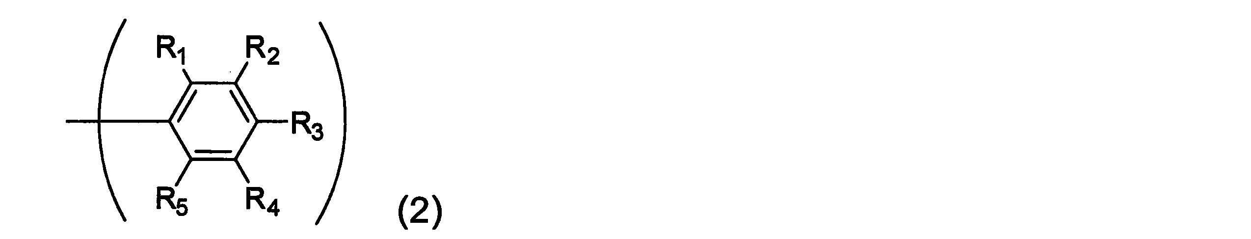
- X in the formula (1) represents, for example, a group represented by the following formula (2).
- R 1 , R 2 , R 3 , R 4 and R 5 are each independently a hydrogen atom, a halogen atom, a hydroxy group, or a linear or branched alkoxy having 1 to 6 carbon atoms) Represents a group.
- the polymer has at least one (for example, one or two) structural units represented by the following formula (3) in the main chain, in addition to having the structure represented by the formula (1) at the terminal. be able to. (Wherein A 1 , A 2 , A 3 , A 4 , A 5 and A 6 each independently represents a hydrogen atom, a methyl group or an ethyl group, Q 1 represents a divalent organic group, m 1 and m 2 represent 0 or 1)
- Q 1 is represented by a divalent organic group represented by the following formula (4), for example.
- Q 2 is an alkylene group having 1 to 10 carbon atoms, an alkenylene group having 2 to 6 carbon atoms, an alicyclic hydrocarbon ring having 3 to 10 carbon atoms, or an aromatic group having 6 to 14 carbon atoms.
- the divalent organic group includes an alkyl group having 1 to 6 carbon atoms, a halogen atom, a hydroxy group, an alkoxy group having 1 to 6 carbon atoms
- the divalent organic group may be substituted with at least one selected from the group consisting of an alkoxycarbonyl group having 2 to 6 carbon atoms, a nitro group, a cyano group, and an alkylthio group having 1 to 6 carbon atoms.
- the hydrocarbon ring includes sulfonyl group, disulfide group, sulfide group, carbonyl group, —C ( ⁇ O) O— group, —O— group, —C (CH 3 ) 2 — group and —C (CF 3 ) 2 —. And may be bonded via a linking group selected from the group consisting of groups, and n 1 and n 2 each independently represents 0 or 1.)
- Q 1 is also represented by a divalent organic group represented by the following formula (5).
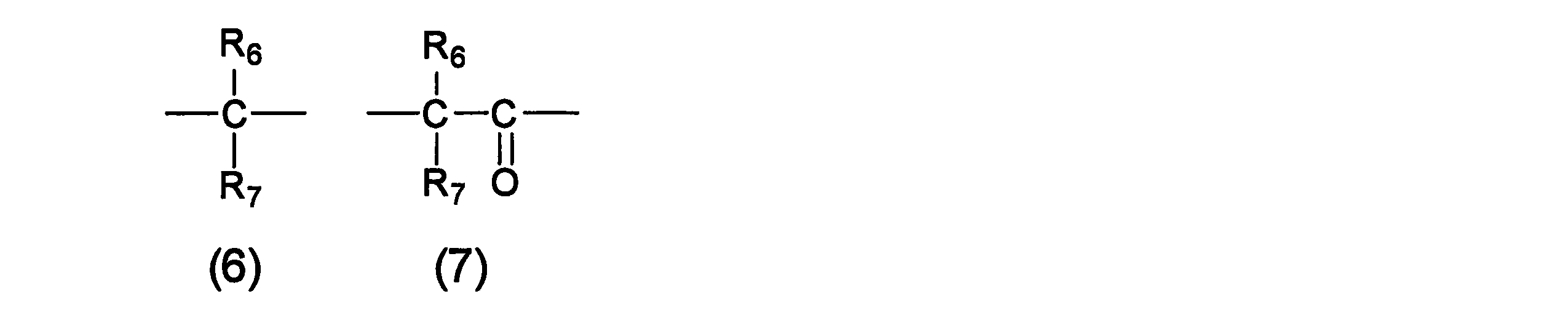
- Y represents a divalent group represented by the following formula (6) or (7).
- R 6 and R 7 each independently represents a hydrogen atom, an alkyl group having 1 to 6 carbon atoms, an alkenyl group having 3 to 6 carbon atoms, a benzyl group or a phenyl group, Substituted with at least one selected from the group consisting of an alkyl group having 1 to 6 carbon atoms, a halogen atom, an alkoxy group having 1 to 6 carbon atoms, a nitro group, a cyano group, and an alkylthio group having 1 to 6 carbon atoms.
- R 6 and R 7 may be bonded to each other to form a ring having 3 to 6 carbon atoms together with the carbon atom bonded to R 6 and R 7 .
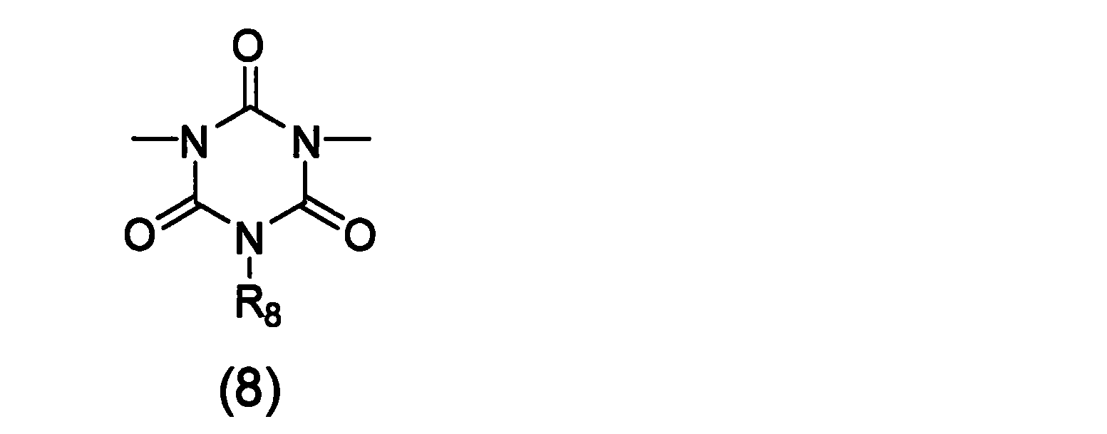
- Q 1 is also represented by a divalent organic group represented by the following formula (8).
- R 8 represents an alkyl group having 1 to 6 carbon atoms, an alkenyl group having 3 to 6 carbon atoms, a benzyl group or a phenyl group, and the phenyl group is an alkyl group having 1 to 6 carbon atoms, (It may be substituted with at least one selected from the group consisting of a halogen atom, an alkoxy group having 1 to 6 carbon atoms, a nitro group, a cyano group, and an alkylthio group having 1 to 6 carbon atoms.)
- Examples of the alkyl group include a methyl group, an ethyl group, and a propyl group.
- Examples of the halogen atom include a fluorine atom, a chlorine atom, a bromine atom, and an iodine atom.
- Examples of the alkoxy group include a methoxy group, ethoxy group, propoxy group, isopropoxy group, butoxy group, isobutoxy group, sec- Examples include butoxy group and tert-butoxy group.
- a fluorine atom and an iodine atom and among these alkoxy groups, a methoxy group is preferable as a substituent because of its excellent EUV absorption ability.
- Examples of the alkylene group include a methylene group, an ethylene group, a propylene group, and a butylene group.
- Examples of the alkenylene group include —CH ⁇ CH— group.
- an allyl group is mentioned, for example.
- Examples of the alicyclic hydrocarbon ring include a cyclopropane ring, a cyclobutane ring, a cyclopentane ring, and a cyclohexane ring.
- Examples of the aromatic hydrocarbon ring include a benzene ring, a naphthalene ring, and an anthracene ring.
- the two alkylene groups, two alkenylene groups, alicyclic hydrocarbon rings or aromatic hydrocarbon rings include a sulfonyl group, a disulfide group, a sulfide group, a carbonyl group, a —C ( ⁇ O) O— group, a —O— group, a —C (CH 3 ) 2 — group, —C ( It may be bonded via a linking group such as a CF 3 ) 2 — group.
- the resist underlayer film forming composition of the first aspect of the present invention may further contain a crosslinking agent and a crosslinking catalyst.
- a resist underlayer film forming composition according to the first aspect of the present invention is applied on a substrate having a film to be processed and baked to form a resist underlayer film.
- the substrate coated with the resist is irradiated with extreme ultraviolet light, then developed to form a resist pattern, and the resist pattern is used as a mask to transfer the pattern onto the substrate by the semiconductor element. It is a method of producing.
- the resist underlayer film forming composition for lithography of the present invention comprises a polymer capped by having the structure represented by the formula (1) at the end. Applying such a resist underlayer film forming composition to an EUV lithography process is effective in reducing the sensitivity and roughness of the resist.
- the resist underlayer film forming composition for lithography of the present invention contains a polymer having a structure represented by the formula (1) at the terminal.
- the weight average molecular weight of the polymer is, for example, 2000 to 50000.
- Examples of the monomer that forms the terminal of the polymer include compounds represented by the following formulas (9-a) to (9-x).
- the polymer is obtained, for example, by reacting a polymer having an epoxy group at a terminal with a monomer that reacts with the epoxy group.
- a monomer that reacts with the epoxy group examples include compounds represented by the above formulas (9-a) to (9-x), that is, 4-fluorobenzoic acid, 4-chlorobenzoic acid, 4-bromobenzoic acid, 4-iodobenzoic acid.
- Examples of the monomer that forms the structural unit represented by the above formula (3) and in which m 1 and m 2 represent 1 include, for example, epoxy groups represented by the following formulas (10-a) to (10-k): A compound having two, That is, diglycidyl 1,4-terephthalate, diglycidyl 2,6-naphthalenedicarboxylate, 1,6-dihydroxynaphthalenediglycidyl, diglycidyl 1,2-cyclohexanedicarboxylate, 2,2-bis (4-hydroxyphenyl) propanedi Glycidyl, 2,2-bis (4-hydroxycyclohexane) propane diglycidyl, 1,4-butanediol diglycidyl, monoallyl isocyanurate diglycidyl, monomethyl isocyanurate diglycidyl, 5,5-diethylbarbiturate diglycidyl, 5,5 -Dimethylhydantoin diglycidyl, but is not limited to these examples.
- Examples of the monomer that forms the structural unit represented by the above formula (3) and in which m 1 and m 2 are 0 are represented by the following formulas (11-a) to (11-s),
- a compound having two carboxyl groups, hydroxyphenyl groups or imide groups, and an acid dianhydride That is, isophthalic acid, 5-hydroxyisophthalic acid, 2,4-dihydroxybenzoic acid, 2,2-bis (4-hydroxyphenyl) sulfone, succinic acid, fumaric acid, tartaric acid, 3,3′-dithiodipropionic acid, 1,4-cyclohexanedicarboxylic acid, cyclobutanoic acid dianhydride, cyclopentanoic acid dianhydride, monoallyl isocyanuric acid, 5,5-diethylbarbituric acid, diglycolic acid, acetone dicarboxylic acid, 2,2'-thiodi Examples include glycolic acid, 4-hydroxybenzoic acid-4-hydroxy
- the number of repeating structural units represented by the formula (3) is, for example, in the range of 10 or more and 10,000 or less.
- Examples of the polymer having at least one type of structural unit represented by the formula (3) and having the structure represented by the formula (1) at the terminal include the following formulas (12-a) to (12-d). ), But is not limited to these examples.
- the polymer having the structural unit represented by the above formula (12-a) and the terminal includes a compound represented by the formula (9-1), a compound represented by the formula (10-h), a formula (11- The compound represented by j) is used as a raw material and polymerized.
- the polymer having a structural unit represented by formula (12-d) and a terminal includes a compound represented by formula (9-r), a compound represented by formula (10-h), a formula (11-j And the compound represented by the above formula) is used as a raw material and polymerized.
- Examples of the organic solvent contained in the resist underlayer film forming composition of the present invention include propylene glycol monomethyl ether (PGME), propylene glycol monomethyl ether acetate (PGMEA), propylene glycol monoethyl ether, propylene glycol monopropyl ether, methyl ethyl ketone, Examples thereof include ethyl lactate, cyclohexanone, ⁇ -butyrolactone, N-methylpyrrolidone, and a mixture of two or more selected from these organic solvents.
- the ratio of the organic solvent with respect to the resist underlayer film forming composition of this invention is 50 to 99.9 mass%, for example.
- the polymer contained in the resist underlayer film forming composition of the present invention is, for example, 0.1% by mass to 50% by mass with respect to the resist underlayer film forming composition.
- the resist underlayer film forming composition of the present invention may contain a crosslinking agent and a crosslinking catalyst that is a compound that promotes a crosslinking reaction.
- the component obtained by removing the organic solvent from the resist underlayer film forming composition of the present invention is defined as a solid content
- the solid content includes an additive such as a polymer and a crosslinking agent and a crosslinking catalyst added as necessary.
- the ratio of the additive is, for example, 0.1% by mass to 50% by mass, preferably 1% by mass to 30% by mass with respect to the solid content of the resist underlayer film forming composition of the present invention.
- crosslinking agent contained as an optional component in the resist underlayer film forming composition of the present invention examples include hexamethoxymethyl melamine, tetramethoxymethyl benzoguanamine, 1,3,4,6-tetrakis (methoxymethyl) glycoluril (POWDERLINK [ 1174), 1,3,4,6-tetrakis (butoxymethyl) glycoluril, 1,3,4,6-tetrakis (hydroxymethyl) glycoluril, 1,3-bis (hydroxymethyl) urea, 1,1,3,3-tetrakis (butoxymethyl) urea and 1,1,3,3-tetrakis (methoxymethyl) urea.
- the content of the cross-linking agent is, for example, 1% by mass to 50% by mass, and preferably 5% by mass to 30% by mass with respect to the polymer.
- Examples of the crosslinking catalyst contained as an optional component in the resist underlayer film forming composition of the present invention include p-toluenesulfonic acid, trifluoromethanesulfonic acid, pyridinium-p-toluenesulfonate, salicylic acid, camphorsulfonic acid, and 5-sulfosalicylic acid.
- Sulfonic acid compounds such as 4-chlorobenzenesulfonic acid, 4-hydroxybenzenesulfonic acid, benzenedisulfonic acid, 1-naphthalenesulfonic acid, citric acid, benzoic acid and hydroxybenzoic acid, and carboxylic acid compounds.
- the content of the crosslinking catalyst is, for example, 0.1% by mass to 50% by mass, and preferably 1% by mass to 30% by mass with respect to the crosslinking agent.
- the substrate used in the method for manufacturing a semiconductor device according to the second aspect of the present invention is typically a silicon wafer, but is an SOI (Silicon on Insulator) substrate, gallium arsenide (GaAs), indium phosphide (A compound semiconductor wafer such as InP) or gallium phosphide (GaP) may be used.
- An insulating film such as a silicon oxide film, a nitrogen-containing silicon oxide film (SiON film), a carbon-containing silicon oxide film (SiOC film), or a fluorine-containing silicon oxide film (SiOF film) is formed on the substrate as a film to be processed. Is formed. In this case, the resist underlayer film is formed on the film to be processed.
- the resist solution used to coat the resist on the resist underlayer film may be either a positive type or a negative type, and a chemically amplified resist sensitive to EUV can be used.
- a developer used for development performed after the EUV irradiation for example, an alkaline developer such as an aqueous solution of tetramethylammonium hydroxide (TMAH) can be used.
- TMAH tetramethylammonium hydroxide
- the weight average molecular weights of the polymers shown in the following Synthesis Examples 1 to 5 in this specification are measurement results by gel permeation chromatography (hereinafter abbreviated as GPC).
- the measurement conditions etc. are as follows using the Tosoh Co., Ltd. product GPC apparatus for a measurement.
- GPC column Shodex (registered trademark) and Asahipak (registered trademark) (Showa Denko KK) Column temperature: 40 ° C Solvent: N, N-dimethylformamide (DMF) Flow rate: 0.6 ml / min Standard sample: Polystyrene (Tosoh Corporation)
- the obtained polymer solution had a weight average molecular weight of 3100 in terms of standard polystyrene.
- the obtained polymer solution had a weight average molecular weight of 5700 in terms of standard polystyrene.
- the obtained polymer solution had a weight average molecular weight of 8,000 in terms of standard polystyrene.
- Example 1 2.50 g of the polymer solution obtained in Synthesis Example 1 above, tetramethoxymethylglycoluril (product name: POWDERLINK [registered trademark] 1174, manufactured by Nippon Cytec Industries Co., Ltd.), p-toluenesulfonic acid monohydrate
- a resist underlayer film forming composition was prepared by mixing 0.01 g, propylene glycol monomethyl ether 19.33 g and propylene glycol monomethyl ether acetate 45.11 g.
- Example 2 2.50 g of the polymer solution obtained in Synthesis Example 2 above, tetramethoxymethylglycoluril (product name: POWDERLINK [registered trademark] 1174, manufactured by Nippon Cytec Industries Co., Ltd.), p-toluenesulfonic acid monohydrate
- a resist underlayer film forming composition was prepared by mixing 0.01 g, propylene glycol monomethyl ether 18.74 g and propylene glycol monomethyl ether acetate 43.74 g.
- Example 3 2.50 g of the polymer solution obtained in Synthesis Example 3 above, tetramethoxymethylglycoluril (product name: POWDERLINK [registered trademark] 1174, manufactured by Nippon Cytec Industries Co., Ltd.), paratoluenesulfonic acid monohydrate
- a resist underlayer film forming composition was prepared by mixing 0.01 g, propylene glycol monomethyl ether 20.57 g and propylene glycol monomethyl ether acetate 48.00 g.
- Example 4 2.50 g of the polymer solution obtained in Synthesis Example 4 above, tetramethoxymethylglycoluril (product name: POWDERLINK [registered trademark] 1174, manufactured by Nippon Cytec Industries Co., Ltd.), paratoluenesulfonic acid monohydrate
- a resist underlayer film forming composition was prepared by mixing 0.01 g, propylene glycol monomethyl ether 20.47 g and propylene glycol monomethyl ether acetate 47.76 g.
- ⁇ Comparative Example 1> 2.50 g of the polymer solution obtained in Synthesis Example 5 above, 0.11 g of tetramethoxymethylglycoluril (product name: POWDERLINK [registered trademark] 1174, manufactured by Nippon Cytec Industries Co., Ltd.), 0.01 g of 5-sulfosalicylic acid, A resist underlayer film forming composition was prepared by mixing 35.70 g of propylene glycol monomethyl ether and 16.19 g of propylene glycol monomethyl ether acetate.
- Each resist underlayer film forming composition prepared in Examples 1 to 4 and Comparative Example 1 of this specification is spin-coated on a silicon wafer so as to have a film thickness of 5 nm and heated at 205 ° C. for 60 seconds. As a result, a resist underlayer film was formed.
- a positive resist solution (methacrylate resin solution) for EUV is spin-coated and heated, and an EUV exposure apparatus (manufactured by EXITETECH, EUV Micro Exposure Lithography Tool, MS-13) is used.
- EUV exposure apparatus 0.35
- Quadropole illumination, ⁇ 0.36 / 0.68.
- PEB After the exposure, PEB was performed, cooled to room temperature on a cooling plate, developed and rinsed, and a resist pattern was formed.
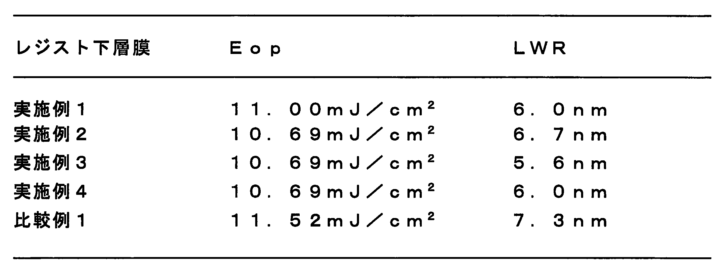
- the evaluation was judged from the optimum exposure dose (Eop) when a line and space of 26 nm was formed, and the LWR value of the pattern by observation from the upper surface of the pattern.
- Eop value the exposure amount when a line and space of 26 nm was formed at the time of optimum focus was defined as the Eop value. Note that the smaller the Eop value, the higher the resist sensitivity, because the desired resist pattern can be formed with less exposure energy.
- LWR For the measurement of LWR, a CD-SEM was used to detect a pattern position two-dimensionally from the top, and the variation in the position was quantified as LWR. Specifically, a line width of 70% of the height from the bottom of the pattern to the top surface of the resist pattern formed in Eop where the 26 nm line and space is formed is set at a plurality of points using a CD-SEM. The length was measured, and 3 ⁇ of those values was taken as the LWR value. Here, ⁇ represents a standard deviation. Note that the smaller the LWR value, the smaller the roughness of the resist to be formed, and the higher the pattern transfer accuracy to the underlying substrate in the manufacturing process.
- the resist underlayer film forming composition when forming a resist underlayer film using the resist underlayer film forming composition of Examples 1 to 4, compared to forming a resist underlayer film using the resist underlayer film forming composition of Comparative Example 1 Since Eop becomes small, the resist underlayer film forming composition can increase the sensitivity of the resist. Further, when the resist underlayer film is formed using the resist underlayer film forming composition of Example 1 to Example 4, the LWR is higher than when the resist underlayer film is formed using the resist underlayer film forming composition of Comparative Example 1. Therefore, the resist underlayer film forming composition can reduce the roughness of the resist pattern to be formed. That is, it was confirmed that the resist underlayer film forming compositions of Examples 1 to 4 showed useful effects for improving resist sensitivity and roughness in the formation of resist patterns.
Landscapes
- Chemical & Material Sciences (AREA)
- Engineering & Computer Science (AREA)
- Chemical Kinetics & Catalysis (AREA)
- Medicinal Chemistry (AREA)
- Polymers & Plastics (AREA)
- Organic Chemistry (AREA)
- Health & Medical Sciences (AREA)
- Architecture (AREA)
- Structural Engineering (AREA)
- Physics & Mathematics (AREA)
- General Physics & Mathematics (AREA)
- Materials For Photolithography (AREA)
- Epoxy Resins (AREA)
- Exposure Of Semiconductors, Excluding Electron Or Ion Beam Exposure (AREA)
Abstract
【課題】 レジスト感度及びレジストパターンのラフネスを改善できるEUV用レジスト下層膜形成組成物を提供する。 【解決手段】 下記式(1)で表される構造を末端に有するポリマー及び有機溶剤を含むリソグラフィー用レジスト下層膜形成組成物。(式中、Xはハロゲン原子、ヒドロキシ基、及び炭素原子数1乃至6の直鎖状又は分岐鎖状のアルコキシ基からなる群から選ばれる少なくも1つで置換されたフェニル基、ナフチル基又はアントラセニル基を表し、vは0又は1を表す。)
Description
本発明は、半導体装置を製造する過程のリソグラフィー工程において、所望の形状のレジストパターンを得るために、基板とその上に形成されるレジスト膜との間にレジスト下層膜を形成するのに有用な組成物に関する。特に、波長13nm乃至14nmの極端紫外線(以下、EUVと略称する。)による露光を用いるリソグラフィー工程に適したレジスト下層膜を形成するための組成物に関するものである。
現在、EUVリソグラフィーは、EUV露光装置におけるEUV露光光源の出力の向上が強く求められている。露光光源の出力が低い場合、目的のレジストパターンを形成するための露光時間が増大することで、単位時間当たりのウエハー処理時間も増大することから、製造工程における生産効率が低下する懸念が生じる。そのため、レジストには、より低いエネルギーの露光量で目的のレジストパターンが精度よく形成されることが要求されている。
低い露光量で目的のレジストパターンを形成させるためには、EUV光がレジストに照射されることで生じる光化学反応がより低いエネルギーで発生し得る必要がある。このように、低い露光量でレジストの光化学反応が生じさせるためには、EUV光に対する高い応答性を有する必要がある。そのため、EUVリソグラフィーにおけるレジスト材料では、このようなレジストの光応答性(感度)を高めることが強く要求されている。
加えて、EUVリソグラフィーの場合、形成されるパターン線幅は32nm以下となり、下地基板へのレジストパターンの転写を精度よく行うためには、形成されるレジストパターンの揺らぎを表す指標であるLine Width Roughness(LWR)及び当該レジストパターンの側壁の揺らぎを表す指標であるLine Edge Roughness(LER)への要求はさらに厳しくなる。形成されたレジストパターン形状が、裾引き形状若しくは隣り合うパターンが分離されずに繋がった形状の場合、又は形成されたレジストパターンが特定方向に対して揺らぎが生じた場合、パターン上方から観察したときのLWR及びLERの値は大きくなり、形成されるレジストパターンの寸法制御に悪影響を与える。そのため、EUVリソグラフィーに使用されるレジスト材料では、このようなレジストパターンの揺らぎ(ラフネス)を低減することが強く要求されている。
これまで、EUVリソグラフィーを指向したレジスト下層膜を形成する材料として、アウトガス発生が低減されたレジスト下層膜形成組成物が開示されている(特許文献1)。また、EUV露光用に特定される材料ではないがジグリシジルエステル化合物と酸二無水物との反応生成物を含むレジスト下層膜形成組成物も開示されている(特許文献2)。しかしながら、これらレジスト下層膜形成組成物ではポリマーの末端をキャッピングして得られるレジスト下層膜形成組成物は例示されておらず、レジストの感度やラフネスを改善する効果については記載されていない。
EUVリソグラフィーにおけるレジスト感度及びラフネスを改善する手法として、レジスト材料に含まれる、樹脂の化学構造又は添加成分の最適化、レジスト形成プロセスにおける露光条件及び現像条件の最適化、などが試みられている。その他、レジストとレジスト下層膜との界面の化学状態をコントロールする手法も挙げられる。すなわち、ポジ型レジストにおいては、レジストとレジスト下層膜の界面の化学状態が塩基状態となる場合、得られるレジストパターン形状が裾引き形状となりやすく、レジストパターンのラフネスも大きくなりやすい。そのため、裾引き形状を補正し、目的寸法のレジストパターンを形成させるためには、より高い露光量を照射する必要があるため、レジスト感度は悪化すると言える。一方、レジストとレジスト下層膜の界面の化学状態が酸性状態となる場合、レジストパターン形状が裾引き形状となることを抑制し、より低い露光量で目的寸法のレジストパターンを形成することができるため、レジスト感度は向上すると言える。
そこで本発明では、レジスト感度及びラフネスを効果的に改善するために、EUVリソグラフィー工程によってレジスト下層膜の表面状態を酸性状態に改質させる、レジスト下層膜形成組成物を提供することを目的とする。
本発明の第一の態様は、下記式(1)で表される構造を末端に有するポリマー及び有機溶剤を含むリソグラフィー用レジスト下層膜形成組成物である。

(式中、Xはハロゲン原子、ヒドロキシ基、及び炭素原子数1乃至6の直鎖状又は分岐鎖状のアルコキシ基からなる群から選ばれる少なくも1つで置換されたフェニル基、ナフチル基又はアントラセニル基を表し、vは0又は1を表す。)
前記式(1)中のXは、例えば下記式(2)で表される基を表す。
(式中、R1、R2、R3、R4及びR5は、それぞれ独立に、水素原子、ハロゲン原子、ヒドロキシ基、又は炭素原子数1乃至6の直鎖状若しくは分岐鎖状のアルコキシ基を表す。)
前記ポリマーは、前記式(1)で表される構造を末端に有する以外に、下記式(3)で表される少なくとも1種(例えば、1種又は2種)の構造単位を主鎖に有することができる。

(式中、A1、A2、A3、A4、A5及びA6は、それぞれ独立に、水素原子、メチル基又はエチル基を表し、Q1は二価の有機基を表し、m1及びm2は0又は1を表す。)
前記式(3)において、Q1は例えば下記式(4)で表される二価の有機基で表される。

(式中、Q2は炭素原子数1乃至10のアルキレン基、炭素原子数2乃至6のアルケニレン基、炭素原子数3乃至10の脂環式炭化水素環又は炭素原子数6乃至14の芳香族炭化水素環を少なくとも1つ有する二価の有機基を表し、前記二価の有機基は、炭素原子数1乃至6のアルキル基、ハロゲン原子、ヒドロキシ基、炭素原子数1乃至6のアルコキシ基、炭素原子数2乃至6のアルコキシカルボニル基、ニトロ基、シアノ基及び炭素原子数1乃至6のアルキルチオ基からなる群から選ばれる少なくとも1つで置換されていてもよく、前記二価の有機基がアルキレン基、アルケニレン基、脂環式炭化水素環又は芳香族炭化水素環を2つ有する場合、該2つのアルキレン基、2つのアルケニレン基、2つの脂環式炭化水素環又は2つの芳香族炭化水素環は、スルホニル基、ジスルフィド基、スルフィド基、カルボニル基,-C(=O)O-基、-O-基、-C(CH3)2-基及び-C(CF3)2-基からなる群から選ばれる連結基を介して結合していてもよく、n1及びn2はそれぞれ独立に0又は1を表す。)
前記式(3)において、Q1は下記式(5)で表される二価の有機基でも表される。

(式中、Yは下記式(6)又は(7)で表される二価の基を表す。)
(式中、R6及びR7はそれぞれ独立に、水素原子、炭素原子数1乃至6のアルキル基、炭素原子数3乃至6のアルケニル基、ベンジル基又はフェニル基を表し、前記フェニル基は、炭素原子数1乃至6のアルキル基、ハロゲン原子、炭素原子数1乃至6のアルコキシ基、ニトロ基、シアノ基及び炭素原子数1乃至6のアルキルチオ基からなる群から選ばれる少なくとも1つで置換されていてもよく、又はR6とR7は互いに結合して、該R6及びR7と結合した炭素原子と共に炭素原子数3乃至6の環を形成していてもよい。)
前記式(3)において、Q1は下記式(8)で表される二価の有機基でも表される。

(式中、R8は炭素原子数1乃至6のアルキル基、炭素原子数3乃至6のアルケニル基、ベンジル基またはフェニル基を表し、前記フェニル基は、炭素原子数1乃至6のアルキル基、ハロゲン原子、炭素原子数1乃至6のアルコキシ基、ニトロ基、シアノ基及び炭素原子数1乃至6のアルキルチオ基からなる群から選ばれる少なくとも1つで置換されていてもよい。)
上記アルキル基としては、例えば、メチル基、エチル基、プロピル基が挙げられる。上記ハロゲン原子としては、例えばフッ素原子、塩素原子、臭素原子、ヨウ素原子が挙げられ、上記アルコキシ基としては、例えばメトキシ基、エトキシ基、プロポキシ基、イソプロポキシ基、ブトキシ基、イソブトキシ基、sec-ブトキシ基、tert-ブトキシ基が挙げられる。これらのハロゲン原子うちフッ素原子及びヨウ素原子、並びにこれらのアルコキシ基のうちメトキシ基は、EUVの吸収能が優れているため、置換基として好ましい。上記アルキレン基としては、例えば、メチレン基、エチレン基、プロピレン基、ブチレン基が挙げられる。上記アルケニレン基としては、例えば-CH=CH-基が挙げられる。上記アルケニル基としては、例えばアリル基が挙げられる。上記脂環式炭化水素環としては、例えば、シクロプロパン環、シクロブタン環、シクロペンタン環、シクロヘキサン環が挙げられる。上記芳香族炭化水素環としては、例えば、ベンゼン環、ナフタレン環、アントラセン環が挙げられる。上記二価の有機基がアルキレン基、アルケニレン基、脂環式炭化水素環又は芳香族炭化水素環を2つ有する場合、当該2つのアルキレン基、2つのアルケニレン基、2つの脂環式炭化水素環又は2つの芳香族炭化水素環は、スルホニル基、ジスルフィド基、スルフィド基、カルボニル基,-C(=O)O-基、-O-基、-C(CH3)2-基、-C(CF3)2-基等の連結基を介して結合していてもよい。
本発明の第一の態様のレジスト下層膜形成組成物は、さらに架橋剤及び架橋触媒を含有してもよい。
本発明の第二の態様は、加工対象膜を有する基板上に、本発明の第一の態様のレジスト下層膜形成組成物を塗布しベークしてレジスト下層膜を形成し、前記レジスト下層膜上にレジストを被覆し、前記レジストで被覆された基板に極端紫外線を照射し、その後現像してレジストパターンを形成し、前記レジストパターンをマスクとしてドライエッチングにより前記基板上にパターンを転写して半導体素子を作製する方法である。
本発明のリソグラフィー用レジスト下層膜形成組成物は、前記式(1)で表される構造を末端に有することによりキャッピングされているポリマーを含有することを特徴とするものである。このようなレジスト下層膜形成組成物をEUVリソグラフィープロセスに適用することは、レジストの感度やラフネスを低減させることに有効である。
本発明のリソグラフィー用レジスト下層膜形成組成物は、前記式(1)で表される構造を末端に有するポリマーを含む。当該ポリマーの重量平均分子量は、例えば2000乃至50000である。
前記ポリマーの末端を形成するモノマーとしては、例えば、下記式(9-a)乃至式(9-x)で表される化合物を挙げることができる。

前記ポリマーは、例えば、末端にエポキシ基を有する重合体と当該エポキシ基に反応するモノマーとを反応させて得られる。このようなモノマーとして、上記式(9-a)乃至式(9-x)で表される化合物、すなわち、4-フルオロ安息香酸、4-クロロ安息香酸、4-ブロモ安息香酸、4-ヨード安息香酸、1-クロロ-4-フルオロ安息香酸、2,4-ジクロロ安息香酸、2,4,6-トリクロロ安息香酸、2,3,4,5,6-ペンタフルオロ安息香酸、4-クロロサリチル酸、3,5-ジクロロサリチル酸、3,5-ジブロモサリチル酸、3,5-ジヨードサリチル酸、テトラクロロ安息香酸無水物、テトラブロモ安息香酸無水物、4-フルオロフェノール、2,4,6-テトラヨードフェノール、4-ヒドロキシ安息香酸、4-メトキシ安息香酸、4-エトキシ安息香酸、4-メトキシフェノール、サリチル酸、3-ヒドロキシ-4-メトキシ安息香酸、3,5-ジメトキシ安息香酸、3,4,5-トリメトキシ安息香酸を例示することができるが、これらの例に限定されるわけではない。これらの化合物の中で好ましくは、4-フルオロ安息香酸、3,5-ジヨードサリチル酸、4-メトキシ安息香酸である。
前記式(3)で表され、m1及びm2が1を表す構造単位を形成するモノマーとしては、例えば、下記式(10-a)乃至式(10-k)で表されるエポキシ基を2つ有する化合物、

すなわち、1,4-テレフタル酸ジグリシジル、2,6-ナフタレンジカルボン酸ジグリシジル、1,6-ジヒドロキシナフタレンジグリシジル、1,2-シクロヘキサンジカルボン酸ジグリシジル、2,2-ビス(4-ヒドロキシフェニル)プロパンジグリシジル、2,2-ビス(4-ヒドロキシシクロヘキサン)プロパンジグリシジル、1,4-ブタンジオールジグリシジル、モノアリルイソシアヌル酸ジグリシジル、モノメチルイソシアヌル酸ジグリシジル、5,5-ジエチルバルビツール酸ジグリシジル、5,5-ジメチルヒダントインジグリシジルが挙げられるが、これらの例に限定されるわけではない。
前記式(3)で表され、m1及びm2が0で表される構造単位を形成するモノマーとしては、例えば、下記式(11-a)乃至式(11-s)で表される、カルボキシル基、ヒドロキシフェニル基又はイミド基を2つ有する化合物、及び酸二無水物、

すなわち、イソフタル酸、5-ヒドロキシイソフタル酸、2,4-ジヒドロキシ安息香酸、2,2-ビス(4-ヒドロキシフェニル)スルホン、コハク酸、フマル酸、酒石酸、3,3’-ジチオジプロピオン酸、1,4-シクロヘキサンジカルボン酸、シクロブタン酸二無水物、シクロペンタン酸二無水物、モノアリルイソシアヌル酸、5,5-ジエチルバルビツール酸、ジグリコール酸、アセトンジカルボン酸、2,2’-チオジグリコール酸、4-ヒドロキシ安息香酸-4-ヒドロキシフェニル、2,2-ビス(4-ヒドロキシフェニル)プロパン、2,2-ビス(4-ヒドロキシフェニル)ヘキサフルオロプロパンが挙げられるが、これらの例に限定されるわけではない。
前記式(3)で表される構造単位の繰り返し数は、例えば10以上10000以下の範囲である。
前記式(3)で表される構造単位を少なくとも1種有し、且つ前記式(1)で表される構造を末端に有するポリマーとしては、下記式(12-a)乃至式(12-d)に例示されるが、これらの例に限定されるわけではない。

上記式(12-a)で表される構造単位及び末端を有するポリマーは、式(9-l)で表される化合物と、式(10-h)で表される化合物と、式(11-j)で表される化合物とを原料に用い、重合させて得られる。式(12-d)で表される構造単位及び末端を有するポリマーは、式(9-r)で表される化合物と、式(10-h)で表される化合物と、式(11-j)で表される化合物とを原料に用い、重合させて得られる。
式(12-a)、式(12-b)、式(12-c)及び式(12-d)のaで表される単位構造とbで表される単位構造とcで表される単位構造のモル比は、a:(b+(c/2))=1:1の関係を満たす。
式(12-a)、式(12-b)、式(12-c)及び式(12-d)に関する前記モル比a:(b+(c/2))=1:1において、bとcのモル比は、b:(c/2)=(1-x):xのように表せる。但し、モル比xは0.01乃至0.8であり、好ましくは0.1乃至0.3である。
本発明のレジスト下層膜形成組成物に含まれる有機溶剤としては、例えば、プロピレングリコールモノメチルエーテル(PGME)、プロピレングリコールモノメチルエーテルアセテート(PGMEA)、プロピレングリコールモノエチルエーテル、プロピレングリコールモノプロピルエーテル、メチルエチルケトン、乳酸エチル、シクロヘキサノン、γ-ブチロラクトン、N-メチルピロリドン、及びこれらの有機溶剤から選択された2種以上の混合物が挙げられる。そして、本発明のレジスト下層膜形成組成物に対する有機溶剤の割合は、例えば50質量%以上99.9質量%以下である。
本発明のレジスト下層膜形成組成物に含まれるポリマーは、当該レジスト下層膜形成組成物に対し例えば0.1質量%乃至50質量%である。
本発明のレジスト下層膜形成組成物は、ポリマー及び有機溶剤の他に、架橋剤、及び架橋反応を促進させる化合物である架橋触媒を含んでもよい。本発明のレジスト下層膜形成組成物から有機溶剤を除いた成分を固形分と定義すると、その固形分はポリマー及び、必要に応じて添加される架橋剤、架橋触媒などの添加物を含む。その添加剤の割合は、本発明のレジスト下層膜形成組成物の固形分に対し、例えば0.1質量%乃至50質量%、好ましくは1質量%乃至30質量%である。
本発明のレジスト下層膜形成組成物に任意成分として含まれる架橋剤としては、例えば、ヘキサメトキシメチルメラミン、テトラメトキシメチルベンゾグアナミン、1,3,4,6-テトラキス(メトキシメチル)グリコールウリル(POWDERLINK〔登録商標〕1174)、1,3,4,6-テトラキス(ブトキシメチル)グリコールウリル、1,3,4,6-テトラキス(ヒドロキシメチル)グリコールウリル、1,3-ビス(ヒドロキシメチル)尿素、1,1,3,3-テトラキス(ブトキシメチル)尿素及び1,1,3,3-テトラキス(メトキシメチル)尿素が挙げられる。上記架橋剤が使用される場合、当該架橋剤の含有割合は、前記ポリマーに対し、例えば1質量%乃至50質量%であり、好ましくは、5質量%乃至30質量%である。
本発明のレジスト下層膜形成組成物に任意成分として含まれる架橋触媒としては、例えば、p-トルエンスルホン酸、トリフルオロメタンスルホン酸、ピリジニウム-p-トルエンスルホネート、サリチル酸、カンファースルホン酸、5-スルホサリチル酸、4-クロロベンゼンスルホン酸、4-ヒドロキシベンゼンスルホン酸、ベンゼンジスルホン酸、1-ナフタレンスルホン酸、クエン酸、安息香酸、ヒドロキシ安息香酸等のスルホン酸化合物及びカルボン酸化合物が挙げられる。上記架橋触媒が使用される場合、当該架橋触媒の含有割合は、前記架橋剤に対し、例えば0.1質量%乃至50質量%であり、好ましくは、1質量%乃至30質量%である。
本発明の第二の態様に係る半導体素子を作製する方法において用いられる基板は、代表的にはシリコンウエハーであるが、SOI(Silicon on Insulator)基板、又は砒化ガリウム(GaAs)、リン化インジウム(InP)、リン化ガリウム(GaP)などの化合物半導体ウエハーを用いてもよい。前記基板上には、加工対象膜として、例えば、酸化珪素膜、窒素含有酸化珪素膜(SiON膜)、炭素含有酸化珪素膜(SiOC膜)、フッ素含有酸化珪素膜(SiOF膜)などの絶縁膜が形成されている。この場合、レジスト下層膜は加工対象膜上に形成される。
本発明の半導体素子を作製する方法において、レジスト下層膜上にレジストを被覆するために用いられるレジスト溶液は、ポジ型、ネガ型いずれでもよく、EUVに感光する化学増幅型レジストを用いることができる。前記EUVの照射後に行われる現像に用いられる現像液として、例えば、テトラメチルアンモニウムヒドロキサイド(TMAH)水溶液のようなアルカリ現像液を用いることができる。
以下、本発明について合成例及び実施例によって具体的に説明する。ただし、本発明は下記合成例及び実施例の記載に限定されるものではない。
本明細書の下記合成例1乃至合成例5に示すポリマーの重量平均分子量は、ゲルパーミエーションクロマトグラフィー(以下、GPCと略称する。)による測定結果である。測定には東ソー(株)製GPC装置を用い、測定条件等は次の通りである。
GPCカラム:Shodex〔登録商標〕・Asahipak〔登録商標〕(昭和電工(株))
カラム温度:40℃
溶媒:N,N-ジメチルホルムアミド(DMF)
流量:0.6ml/分
標準試料:ポリスチレン(東ソー(株))
GPCカラム:Shodex〔登録商標〕・Asahipak〔登録商標〕(昭和電工(株))
カラム温度:40℃
溶媒:N,N-ジメチルホルムアミド(DMF)
流量:0.6ml/分
標準試料:ポリスチレン(東ソー(株))
<合成例1>
モノメチルジグリシジルイソシアヌル酸(製品名:Me-DGIC、四国化成工業(株))12.32g、1,2,3,4-シクロブタンテトラカルボン酸二無水物7.86g、3,5-ジヨードサリチル酸5.51g、ベンジルトリエチルアンモニウムクロライド0.54g及びプロピレングリコールモノメチルエーテル104.89gを混合し、撹拌しながら4時間加熱還流した。得られたポリマー溶液に、陽イオン交換樹脂(製品名:ダウエックス〔登録商標〕550A、ムロマチテクノス(株))26g及び陰イオン交換樹脂(製品名:アンバーライト〔登録商標〕15JWET、オルガノ(株))26gを加えて、室温で4時間イオン交換処理した。GPC分析の結果、得られたポリマー溶液は標準ポリスチレン換算にて重量平均分子量3100であった。
モノメチルジグリシジルイソシアヌル酸(製品名:Me-DGIC、四国化成工業(株))12.32g、1,2,3,4-シクロブタンテトラカルボン酸二無水物7.86g、3,5-ジヨードサリチル酸5.51g、ベンジルトリエチルアンモニウムクロライド0.54g及びプロピレングリコールモノメチルエーテル104.89gを混合し、撹拌しながら4時間加熱還流した。得られたポリマー溶液に、陽イオン交換樹脂(製品名:ダウエックス〔登録商標〕550A、ムロマチテクノス(株))26g及び陰イオン交換樹脂(製品名:アンバーライト〔登録商標〕15JWET、オルガノ(株))26gを加えて、室温で4時間イオン交換処理した。GPC分析の結果、得られたポリマー溶液は標準ポリスチレン換算にて重量平均分子量3100であった。
<合成例2>
モノアリルジグリシジルイソシアヌル酸(製品名:MA-DGIC、四国化成工業(株))4.50g、1,2,3,4-シクロブタンテトラカルボン酸二無水物2.71g、3,5-ジヨードサリチル酸1.90g、ベンジルトリエチルアンモニウムクロライド0.19g及びプロピレングリコールモノメチルエーテル37.18gを混合し、撹拌しながら4時間加熱還流した。得られたポリマー溶液に、陽イオン交換樹脂(製品名:ダウエックス〔登録商標〕550A、ムロマチテクノス(株))9g及び陰イオン交換樹脂(製品名:アンバーライト〔登録商標〕15JWET、オルガノ(株))9gを加えて、室温で4時間イオン交換処理した。GPC分析の結果、得られたポリマー溶液は標準ポリスチレン換算にて重量平均分子量3100であった。
モノアリルジグリシジルイソシアヌル酸(製品名:MA-DGIC、四国化成工業(株))4.50g、1,2,3,4-シクロブタンテトラカルボン酸二無水物2.71g、3,5-ジヨードサリチル酸1.90g、ベンジルトリエチルアンモニウムクロライド0.19g及びプロピレングリコールモノメチルエーテル37.18gを混合し、撹拌しながら4時間加熱還流した。得られたポリマー溶液に、陽イオン交換樹脂(製品名:ダウエックス〔登録商標〕550A、ムロマチテクノス(株))9g及び陰イオン交換樹脂(製品名:アンバーライト〔登録商標〕15JWET、オルガノ(株))9gを加えて、室温で4時間イオン交換処理した。GPC分析の結果、得られたポリマー溶液は標準ポリスチレン換算にて重量平均分子量3100であった。
<合成例3>
モノメチルジグリシジルイソシアヌル酸(製品名:Me-DGIC、四国化成工業(株))4.93g、1,2,3,4-シクロブタンテトラカルボン酸二無水物3.33g、4-フロオロ安息香酸0.53g、ベンジルトリエチルアンモニウムクロライド0.21g及びプロピレングリコールモノメチルエーテル35.99gを混合し、撹拌しながら4時間加熱還流した。得られたポリマー溶液に、陽イオン交換樹脂(製品名:ダウエックス〔登録商標〕550A、ムロマチテクノス(株))26g及び陰イオン交換樹脂(製品名:アンバーライト〔登録商標〕10JWET、オルガノ(株))10gを加えて、室温で4時間イオン交換処理した。GPC分析の結果、得られたポリマー溶液は標準ポリスチレン換算にて重量平均分子量4500であった。
モノメチルジグリシジルイソシアヌル酸(製品名:Me-DGIC、四国化成工業(株))4.93g、1,2,3,4-シクロブタンテトラカルボン酸二無水物3.33g、4-フロオロ安息香酸0.53g、ベンジルトリエチルアンモニウムクロライド0.21g及びプロピレングリコールモノメチルエーテル35.99gを混合し、撹拌しながら4時間加熱還流した。得られたポリマー溶液に、陽イオン交換樹脂(製品名:ダウエックス〔登録商標〕550A、ムロマチテクノス(株))26g及び陰イオン交換樹脂(製品名:アンバーライト〔登録商標〕10JWET、オルガノ(株))10gを加えて、室温で4時間イオン交換処理した。GPC分析の結果、得られたポリマー溶液は標準ポリスチレン換算にて重量平均分子量4500であった。
<合成例4>
モノアリルジグリシジルイソシアヌル酸(製品名:MA-DGIC、四国化成工業(株))5.50g、1,2,3,4-シクロブタンテトラカルボン酸二無水物3.31g、4-メトキシ安息香酸0.91g、ベンジルトリエチルアンモニウムクロライド0.23g及びプロピレングリコールモノメチルエーテル39.77gを混合し、撹拌しながら4時間加熱還流した。得られたポリマー溶液に、陽イオン交換樹脂(製品名:ダウエックス〔登録商標〕550A、ムロマチテクノス(株))10g及び陰イオン交換樹脂(製品名:アンバーライト〔登録商標〕15JWET、オルガノ(株))10gを加えて、室温で4時間イオン交換処理した。GPC分析の結果、得られたポリマー溶液は標準ポリスチレン換算にて重量平均分子量5700であった。
モノアリルジグリシジルイソシアヌル酸(製品名:MA-DGIC、四国化成工業(株))5.50g、1,2,3,4-シクロブタンテトラカルボン酸二無水物3.31g、4-メトキシ安息香酸0.91g、ベンジルトリエチルアンモニウムクロライド0.23g及びプロピレングリコールモノメチルエーテル39.77gを混合し、撹拌しながら4時間加熱還流した。得られたポリマー溶液に、陽イオン交換樹脂(製品名:ダウエックス〔登録商標〕550A、ムロマチテクノス(株))10g及び陰イオン交換樹脂(製品名:アンバーライト〔登録商標〕15JWET、オルガノ(株))10gを加えて、室温で4時間イオン交換処理した。GPC分析の結果、得られたポリマー溶液は標準ポリスチレン換算にて重量平均分子量5700であった。
<合成例5>
モノアリルジグリシジルイソシアヌル酸(製品名:MA-DGIC、四国化成工業(株))13.00g、5,5-ジエチルバルビツール酸8.65g、ベンジルトリエチルアンモニウムクロライド0.53g及びプロピレングリコールモノメチルエーテル88.72gを混合し、撹拌しながら4時間加熱還流した。得られたポリマー溶液に、陽イオン交換樹脂(製品名:ダウエックス〔登録商標〕550A、ムロマチテクノス(株))22g及び陰イオン交換樹脂(製品名:アンバーライト〔登録商標〕15JWET、オルガノ(株))22gを加えて、室温で4時間イオン交換処理した。GPC分析の結果、得られたポリマー溶液は標準ポリスチレン換算にて重量平均分子量8000であった。
モノアリルジグリシジルイソシアヌル酸(製品名:MA-DGIC、四国化成工業(株))13.00g、5,5-ジエチルバルビツール酸8.65g、ベンジルトリエチルアンモニウムクロライド0.53g及びプロピレングリコールモノメチルエーテル88.72gを混合し、撹拌しながら4時間加熱還流した。得られたポリマー溶液に、陽イオン交換樹脂(製品名:ダウエックス〔登録商標〕550A、ムロマチテクノス(株))22g及び陰イオン交換樹脂(製品名:アンバーライト〔登録商標〕15JWET、オルガノ(株))22gを加えて、室温で4時間イオン交換処理した。GPC分析の結果、得られたポリマー溶液は標準ポリスチレン換算にて重量平均分子量8000であった。
<実施例1>
上記合成例1で得られたポリマー溶液2.50g、テトラメトキシメチルグリコールウリル(製品名:POWDERLINK〔登録商標〕1174、日本サイテックインダストリーズ(株)製)0.13g、パラトルエンスルホン酸一水和物0.01g、プロピレングリコールモノメチルエーテル19.33g及びプロピレングリコールモノメチルエーテルアセテート45.11gを混合することで、レジスト下層膜形成組成物を調製した。
上記合成例1で得られたポリマー溶液2.50g、テトラメトキシメチルグリコールウリル(製品名:POWDERLINK〔登録商標〕1174、日本サイテックインダストリーズ(株)製)0.13g、パラトルエンスルホン酸一水和物0.01g、プロピレングリコールモノメチルエーテル19.33g及びプロピレングリコールモノメチルエーテルアセテート45.11gを混合することで、レジスト下層膜形成組成物を調製した。
<実施例2>
上記合成例2で得られたポリマー溶液2.50g、テトラメトキシメチルグリコールウリル(製品名:POWDERLINK〔登録商標〕1174、日本サイテックインダストリーズ(株)製)0.12g、パラトルエンスルホン酸一水和物0.01g、プロピレングリコールモノメチルエーテル18.74g及びプロピレングリコールモノメチルエーテルアセテート43.74gを混合することで、レジスト下層膜形成組成物を調製した。
上記合成例2で得られたポリマー溶液2.50g、テトラメトキシメチルグリコールウリル(製品名:POWDERLINK〔登録商標〕1174、日本サイテックインダストリーズ(株)製)0.12g、パラトルエンスルホン酸一水和物0.01g、プロピレングリコールモノメチルエーテル18.74g及びプロピレングリコールモノメチルエーテルアセテート43.74gを混合することで、レジスト下層膜形成組成物を調製した。
<実施例3>
上記合成例3で得られたポリマー溶液2.50g、テトラメトキシメチルグリコールウリル(製品名:POWDERLINK〔登録商標〕1174、日本サイテックインダストリーズ(株)製)0.14g、パラトルエンスルホン酸一水和物0.01g、プロピレングリコールモノメチルエーテル20.57g及びプロピレングリコールモノメチルエーテルアセテート48.00gを混合することで、レジスト下層膜形成組成物を調製した。
上記合成例3で得られたポリマー溶液2.50g、テトラメトキシメチルグリコールウリル(製品名:POWDERLINK〔登録商標〕1174、日本サイテックインダストリーズ(株)製)0.14g、パラトルエンスルホン酸一水和物0.01g、プロピレングリコールモノメチルエーテル20.57g及びプロピレングリコールモノメチルエーテルアセテート48.00gを混合することで、レジスト下層膜形成組成物を調製した。
<実施例4>
上記合成例4で得られたポリマー溶液2.50g、テトラメトキシメチルグリコールウリル(製品名:POWDERLINK〔登録商標〕1174、日本サイテックインダストリーズ(株)製)0.14g、パラトルエンスルホン酸一水和物0.01g、プロピレングリコールモノメチルエーテル20.47g及びプロピレングリコールモノメチルエーテルアセテート47.76gを混合することで、レジスト下層膜形成組成物を調製した。
上記合成例4で得られたポリマー溶液2.50g、テトラメトキシメチルグリコールウリル(製品名:POWDERLINK〔登録商標〕1174、日本サイテックインダストリーズ(株)製)0.14g、パラトルエンスルホン酸一水和物0.01g、プロピレングリコールモノメチルエーテル20.47g及びプロピレングリコールモノメチルエーテルアセテート47.76gを混合することで、レジスト下層膜形成組成物を調製した。
<比較例1>
上記合成例5で得られたポリマー溶液2.50g、テトラメトキシメチルグリコールウリル(製品名:POWDERLINK〔登録商標〕1174、日本サイテックインダストリーズ(株)製)0.11g、5-スルホサリチル酸0.01g、プロピレングリコールモノメチルエーテル35.70g及びプロピレングリコールモノメチルエーテルアセテート16.19gを混合することで、レジスト下層膜形成組成物を調製した。
上記合成例5で得られたポリマー溶液2.50g、テトラメトキシメチルグリコールウリル(製品名:POWDERLINK〔登録商標〕1174、日本サイテックインダストリーズ(株)製)0.11g、5-スルホサリチル酸0.01g、プロピレングリコールモノメチルエーテル35.70g及びプロピレングリコールモノメチルエーテルアセテート16.19gを混合することで、レジスト下層膜形成組成物を調製した。
(レジストパターンの形成及び評価)
シリコンウエハー上に、本明細書の実施例1乃至実施例4及び比較例1で調製された各レジスト下層膜形成組成物を膜厚5nmとなるようにスピンコートし、205℃で60秒間加熱することにより、レジスト下層膜を形成した。そのレジスト下層膜上に、EUV用ポジ型レジスト溶液(メタクリレート系樹脂溶液)をスピンコートして加熱を行い、EUV露光装置(EXITECH社製、EUV Micro Exposure Lithography Tool、MS-13)を用い、NA=0.35、Quadropole照明、σ=0.36/0.68の条件で露光した。露光後、PEBを行い、クーリングプレート上で室温まで冷却し、現像及びリンス処理をし、レジストパターンを形成した。評価は、26nmのラインアンドスペースが形成される際の最適露光量(Eop)、及びパターン上面からの観察によるパターンのLWR値から判断した。
シリコンウエハー上に、本明細書の実施例1乃至実施例4及び比較例1で調製された各レジスト下層膜形成組成物を膜厚5nmとなるようにスピンコートし、205℃で60秒間加熱することにより、レジスト下層膜を形成した。そのレジスト下層膜上に、EUV用ポジ型レジスト溶液(メタクリレート系樹脂溶液)をスピンコートして加熱を行い、EUV露光装置(EXITECH社製、EUV Micro Exposure Lithography Tool、MS-13)を用い、NA=0.35、Quadropole照明、σ=0.36/0.68の条件で露光した。露光後、PEBを行い、クーリングプレート上で室温まで冷却し、現像及びリンス処理をし、レジストパターンを形成した。評価は、26nmのラインアンドスペースが形成される際の最適露光量(Eop)、及びパターン上面からの観察によるパターンのLWR値から判断した。
Eopの評価は、Critical Dimension Scanning Electron Microscopy(CD-SEM)を用い、最適フォーカス時において26nmのラインアンドスペースが形成される際の露光量をEop値とした。尚、Eop値が小さいほど、少ない露光エネルギーで目的のレジストパターンを形成することができるため、レジスト感度が高くなる。
LWRの測定は、CD-SEMを用い、パターン位置を上部から二次元的に検出し、その位置のばらつきをLWRとして定量化した。具体的には、前記の26nmのラインアンドスペースが形成されるEopにおいて形成されたレジストパターンの、パターン底部から上面までの高さの70%の部位の線幅をCD-SEMを用いて複数ポイント測長し、それらの値の3σをLWR値とした。ここで、σは標準偏差を表す。尚、LWR値が小さいほど、形成されるレジストのラフネスが小さくなり、製造工程における下地基板へのパターン転写精度を高めることができる。
26nmのラインアンドスペースにおけるレジストパターンのEopとLWRの測定結果を下記表1に示す。このEopとLWRはその値が小さいほど好ましい。
[表1]
[表1]
表1より、実施例1乃至実施例4のレジスト下層膜形成組成物を用いてレジスト下層膜を形成した場合、比較例1のレジスト下層膜形成組成物を用いてレジスト下層膜を形成した場合よりもEopが小さくなることから、当該レジスト下層膜形成組成物はレジストの感度を高めることができる。また、実施例1乃至実施例4のレジスト下層膜形成組成物を用いてレジスト下層膜を形成した場合、比較例1のレジスト下層膜形成組成物を用いてレジスト下層膜を形成した場合よりもLWRが小さいことから、当該レジスト下層膜形成組成物は形成されるレジストパターンのラフネスを低減することができる。すなわち、実施例1乃至実施例4のレジスト下層膜形成組成物は、レジストパターンの形成においてレジストの感度及びラフネスを改善するために有用な効果を示すことが確認された。
以上、本発明の実施形態を説明したが、本発明の技術的範囲は上記実施形態に記載された範囲には限定されない。上記実施形態に、多様な変更又は改良を加えることが可能である。
Claims (8)
- 下記式(1)で表される構造を末端に有するポリマー及び有機溶剤を含むリソグラフィー用レジスト下層膜形成組成物。

- 前記式(1)中のXは下記式(2)で表される基を表す請求項1に記載のリソグラフィー用レジスト下層膜形成組成物。

- 前記ポリマーは下記式(3)で表される少なくとも1種の構造単位を主鎖に有する請求項1又は請求項2に記載のリソグラフィー用レジスト下層膜形成組成物。

- 前記式(3)において、Q1は下記式(4)で表される二価の有機基を表す請求項3に記載のリソグラフィー用レジスト下層膜形成組成物。

- 前記式(3)において、Q1は下記式(5)で表される二価の有機基を表す請求項3に記載のリソグラフィー用レジスト下層膜形成組成物。


- 前記式(3)において、Q1は下記式(8)で表される二価の有機基を表す請求項3に記載のリソグラフィー用レジスト下層膜形成組成物。
- さらに架橋剤及び架橋触媒を含む請求項1乃至請求項6のいずれか一項に記載のリソグラフィー用レジスト下層膜形成組成物。
- 加工対象膜を有する基板上に、請求項1乃至請求項7のいずれか一項に記載のレジスト下層膜形成組成物を塗布しベークしてレジスト下層膜を形成し、前記レジスト下層膜上にレジストを被覆し、前記レジストで被覆された基板に極端紫外線を照射し、その後現像してレジストパターンを形成し、前記レジストパターンをマスクとしてドライエッチングにより前記基板上にパターンを転写して半導体素子を作製する方法。
Priority Applications (1)
| Application Number | Priority Date | Filing Date | Title |
|---|---|---|---|
| JP2014506123A JP6083537B2 (ja) | 2012-03-23 | 2013-03-05 | Euvリソグラフィー用レジスト下層膜形成組成物 |
Applications Claiming Priority (2)
| Application Number | Priority Date | Filing Date | Title |
|---|---|---|---|
| JP2012-067599 | 2012-03-23 | ||
| JP2012067599 | 2012-03-23 |
Publications (1)
| Publication Number | Publication Date |
|---|---|
| WO2013141015A1 true WO2013141015A1 (ja) | 2013-09-26 |
Family
ID=49222477
Family Applications (1)
| Application Number | Title | Priority Date | Filing Date |
|---|---|---|---|
| PCT/JP2013/055971 WO2013141015A1 (ja) | 2012-03-23 | 2013-03-05 | Euvリソグラフィー用レジスト下層膜形成組成物 |
Country Status (3)
| Country | Link |
|---|---|
| JP (1) | JP6083537B2 (ja) |
| TW (1) | TWI627508B (ja) |
| WO (1) | WO2013141015A1 (ja) |
Cited By (16)
| Publication number | Priority date | Publication date | Assignee | Title |
|---|---|---|---|---|
| WO2015046149A1 (ja) * | 2013-09-27 | 2015-04-02 | 日産化学工業株式会社 | レジスト下層膜形成組成物及びそれを用いたレジストパターンの形成方法 |
| WO2015163195A1 (ja) * | 2014-04-25 | 2015-10-29 | 日産化学工業株式会社 | レジスト下層膜形成組成物及びそれを用いたレジストパターンの形成方法 |
| WO2019138823A1 (ja) * | 2018-01-09 | 2019-07-18 | Jsr株式会社 | パターニングされた基板の製造方法 |
| US20210003917A1 (en) * | 2019-07-02 | 2021-01-07 | Shin-Etsu Chemical Co., Ltd. | Positive resist composition and patterning process |
| US20210033971A1 (en) * | 2019-08-02 | 2021-02-04 | Shin-Etsu Chemical Co., Ltd. | Positive resist composition and patterning process |
| US20210048747A1 (en) * | 2019-08-14 | 2021-02-18 | Shin-Etsu Chemical Co., Ltd. | Chemically amplified resist composition and patterning process |
| WO2021111976A1 (ja) * | 2019-12-04 | 2021-06-10 | 日産化学株式会社 | ポリマーの製造方法 |
| CN113126432A (zh) * | 2019-12-31 | 2021-07-16 | 罗门哈斯电子材料韩国有限公司 | 用于光致抗蚀剂底层的涂料组合物 |
| WO2022172917A1 (ja) * | 2021-02-09 | 2022-08-18 | 日産化学株式会社 | アリール基で封止された側鎖含有ポリマーを含むレジスト下層膜形成組成物 |
| US11675271B2 (en) | 2020-01-31 | 2023-06-13 | Samsung Sdi Co., Ltd. | Resist underlayer composition, and method of forming patterns using the composition |
| WO2023145703A1 (ja) * | 2022-01-25 | 2023-08-03 | 日産化学株式会社 | 末端封止ポリマーを含むレジスト下層膜形成組成物 |
| US11860540B2 (en) | 2020-05-18 | 2024-01-02 | Shin-Etsu Chemical Co., Ltd. | Positive resist composition and patterning process |
| KR20240009413A (ko) | 2021-05-19 | 2024-01-22 | 제이에스알 가부시끼가이샤 | 반도체 기판의 제조 방법 및 레지스트 하층막 형성용 조성물 |
| KR20240018455A (ko) | 2021-06-07 | 2024-02-13 | 제이에스알 가부시끼가이샤 | 반도체 기판의 제조 방법 및 레지스트 하층막 형성용 조성물 |
| KR20240041932A (ko) | 2021-08-10 | 2024-04-01 | 제이에스알 가부시끼가이샤 | 반도체 기판의 제조 방법 및 레지스트 하층막 형성용 조성물 |
| US11987561B2 (en) | 2020-01-17 | 2024-05-21 | Samsung Sdi Co., Ltd. | Resist underlayer composition, and method of forming patterns using the composition |
Families Citing this family (2)
| Publication number | Priority date | Publication date | Assignee | Title |
|---|---|---|---|---|
| KR102400603B1 (ko) * | 2019-03-29 | 2022-05-19 | 삼성에스디아이 주식회사 | 레지스트 하층막용 조성물 및 이를 이용한 패턴 형성 방법 |
| KR102499391B1 (ko) | 2019-12-31 | 2023-02-10 | 삼성에스디아이 주식회사 | 초박막 형성이 가능한 레지스트 하층막 조성물 |
Citations (7)
| Publication number | Priority date | Publication date | Assignee | Title |
|---|---|---|---|---|
| JP2004250377A (ja) * | 2003-02-20 | 2004-09-09 | Maruzen Petrochem Co Ltd | チオール化合物、共重合体及び共重合体の製造方法 |
| JP2006184471A (ja) * | 2004-12-27 | 2006-07-13 | Sanyo Electric Co Ltd | リソグラフィ用反射防止膜形成組成物及びレジストパターンの形成方法 |
| JP2006343416A (ja) * | 2005-06-07 | 2006-12-21 | Tokyo Ohka Kogyo Co Ltd | 反射防止膜形成用組成物、それを用いた反射防止膜 |
| JP2009175436A (ja) * | 2008-01-24 | 2009-08-06 | Nissan Chem Ind Ltd | バリア性を示すレジスト下層膜の形成用組成物及びレジスト下層膜のバリア性評価方法 |
| WO2010122948A1 (ja) * | 2009-04-21 | 2010-10-28 | 日産化学工業株式会社 | Euvリソグラフィー用レジスト下層膜形成組成物 |
| WO2011074494A1 (ja) * | 2009-12-14 | 2011-06-23 | 日産化学工業株式会社 | レジスト下層膜形成組成物 |
| WO2012124597A1 (ja) * | 2011-03-15 | 2012-09-20 | 日産化学工業株式会社 | レジスト下層膜形成組成物及びそれを用いたレジストパターンの形成方法 |
Family Cites Families (3)
| Publication number | Priority date | Publication date | Assignee | Title |
|---|---|---|---|---|
| KR101189397B1 (ko) * | 2003-10-15 | 2012-10-11 | 브레우어 사이언스 인코포레이션 | 비아-퍼스트 듀얼 다마신 적용예에서 사용되는 현상제에 용해성인 물질 및 상기 물질 사용 방법 |
| JP5333737B2 (ja) * | 2009-02-03 | 2013-11-06 | 日産化学工業株式会社 | レジスト下層膜形成組成物及びそれを用いたレジストパターンの形成方法 |
| US8501383B2 (en) * | 2009-05-20 | 2013-08-06 | Rohm And Haas Electronic Materials Llc | Coating compositions for use with an overcoated photoresist |
-
2013
- 2013-03-05 WO PCT/JP2013/055971 patent/WO2013141015A1/ja active Application Filing
- 2013-03-05 JP JP2014506123A patent/JP6083537B2/ja active Active
- 2013-03-19 TW TW102109627A patent/TWI627508B/zh active
Patent Citations (7)
| Publication number | Priority date | Publication date | Assignee | Title |
|---|---|---|---|---|
| JP2004250377A (ja) * | 2003-02-20 | 2004-09-09 | Maruzen Petrochem Co Ltd | チオール化合物、共重合体及び共重合体の製造方法 |
| JP2006184471A (ja) * | 2004-12-27 | 2006-07-13 | Sanyo Electric Co Ltd | リソグラフィ用反射防止膜形成組成物及びレジストパターンの形成方法 |
| JP2006343416A (ja) * | 2005-06-07 | 2006-12-21 | Tokyo Ohka Kogyo Co Ltd | 反射防止膜形成用組成物、それを用いた反射防止膜 |
| JP2009175436A (ja) * | 2008-01-24 | 2009-08-06 | Nissan Chem Ind Ltd | バリア性を示すレジスト下層膜の形成用組成物及びレジスト下層膜のバリア性評価方法 |
| WO2010122948A1 (ja) * | 2009-04-21 | 2010-10-28 | 日産化学工業株式会社 | Euvリソグラフィー用レジスト下層膜形成組成物 |
| WO2011074494A1 (ja) * | 2009-12-14 | 2011-06-23 | 日産化学工業株式会社 | レジスト下層膜形成組成物 |
| WO2012124597A1 (ja) * | 2011-03-15 | 2012-09-20 | 日産化学工業株式会社 | レジスト下層膜形成組成物及びそれを用いたレジストパターンの形成方法 |
Cited By (28)
| Publication number | Priority date | Publication date | Assignee | Title |
|---|---|---|---|---|
| TWI656167B (zh) * | 2013-09-27 | 2019-04-11 | 日商日產化學工業股份有限公司 | 光阻下層膜形成組成物及使用其之光阻圖型之形成方法 |
| WO2015046149A1 (ja) * | 2013-09-27 | 2015-04-02 | 日産化学工業株式会社 | レジスト下層膜形成組成物及びそれを用いたレジストパターンの形成方法 |
| CN105579909A (zh) * | 2013-09-27 | 2016-05-11 | 日产化学工业株式会社 | 抗蚀剂下层膜形成用组合物和使用其的抗蚀剂图案的形成方法 |
| US9448480B2 (en) | 2013-09-27 | 2016-09-20 | Nissan Chemical Industries, Ltd. | Resist underlayer film formation composition and method for forming resist pattern using the same |
| JPWO2015046149A1 (ja) * | 2013-09-27 | 2017-03-09 | 日産化学工業株式会社 | レジスト下層膜形成組成物及びそれを用いたレジストパターンの形成方法 |
| US9910354B2 (en) | 2014-04-25 | 2018-03-06 | Nissan Chemical Industries, Ltd. | Resist underlayer film-forming composition and method for forming resist pattern using the same |
| JPWO2015163195A1 (ja) * | 2014-04-25 | 2017-04-13 | 日産化学工業株式会社 | レジスト下層膜形成組成物及びそれを用いたレジストパターンの形成方法 |
| WO2015163195A1 (ja) * | 2014-04-25 | 2015-10-29 | 日産化学工業株式会社 | レジスト下層膜形成組成物及びそれを用いたレジストパターンの形成方法 |
| WO2019138823A1 (ja) * | 2018-01-09 | 2019-07-18 | Jsr株式会社 | パターニングされた基板の製造方法 |
| KR20200106499A (ko) * | 2018-01-09 | 2020-09-14 | 제이에스알 가부시끼가이샤 | 패터닝된 기판의 제조 방법 |
| KR102646535B1 (ko) * | 2018-01-09 | 2024-03-13 | 제이에스알 가부시끼가이샤 | 패터닝된 기판의 제조 방법 |
| US11567406B2 (en) * | 2019-07-02 | 2023-01-31 | Shin-Etsu Chemical Co., Ltd. | Positive resist composition and patterning process |
| US20210003917A1 (en) * | 2019-07-02 | 2021-01-07 | Shin-Etsu Chemical Co., Ltd. | Positive resist composition and patterning process |
| US20210033971A1 (en) * | 2019-08-02 | 2021-02-04 | Shin-Etsu Chemical Co., Ltd. | Positive resist composition and patterning process |
| US11586110B2 (en) * | 2019-08-02 | 2023-02-21 | Shin-Etsu Chemical Co., Ltd. | Positive resist composition and patterning process |
| US11720018B2 (en) * | 2019-08-14 | 2023-08-08 | Shin-Etsu Chemical Co., Ltd. | Chemically amplified resist composition and patterning process |
| US20210048747A1 (en) * | 2019-08-14 | 2021-02-18 | Shin-Etsu Chemical Co., Ltd. | Chemically amplified resist composition and patterning process |
| CN114746468A (zh) * | 2019-12-04 | 2022-07-12 | 日产化学株式会社 | 聚合物的制造方法 |
| WO2021111976A1 (ja) * | 2019-12-04 | 2021-06-10 | 日産化学株式会社 | ポリマーの製造方法 |
| CN113126432A (zh) * | 2019-12-31 | 2021-07-16 | 罗门哈斯电子材料韩国有限公司 | 用于光致抗蚀剂底层的涂料组合物 |
| US11987561B2 (en) | 2020-01-17 | 2024-05-21 | Samsung Sdi Co., Ltd. | Resist underlayer composition, and method of forming patterns using the composition |
| US11675271B2 (en) | 2020-01-31 | 2023-06-13 | Samsung Sdi Co., Ltd. | Resist underlayer composition, and method of forming patterns using the composition |
| US11860540B2 (en) | 2020-05-18 | 2024-01-02 | Shin-Etsu Chemical Co., Ltd. | Positive resist composition and patterning process |
| WO2022172917A1 (ja) * | 2021-02-09 | 2022-08-18 | 日産化学株式会社 | アリール基で封止された側鎖含有ポリマーを含むレジスト下層膜形成組成物 |
| KR20240009413A (ko) | 2021-05-19 | 2024-01-22 | 제이에스알 가부시끼가이샤 | 반도체 기판의 제조 방법 및 레지스트 하층막 형성용 조성물 |
| KR20240018455A (ko) | 2021-06-07 | 2024-02-13 | 제이에스알 가부시끼가이샤 | 반도체 기판의 제조 방법 및 레지스트 하층막 형성용 조성물 |
| KR20240041932A (ko) | 2021-08-10 | 2024-04-01 | 제이에스알 가부시끼가이샤 | 반도체 기판의 제조 방법 및 레지스트 하층막 형성용 조성물 |
| WO2023145703A1 (ja) * | 2022-01-25 | 2023-08-03 | 日産化学株式会社 | 末端封止ポリマーを含むレジスト下層膜形成組成物 |
Also Published As
| Publication number | Publication date |
|---|---|
| TWI627508B (zh) | 2018-06-21 |
| JPWO2013141015A1 (ja) | 2015-08-03 |
| TW201400987A (zh) | 2014-01-01 |
| JP6083537B2 (ja) | 2017-02-22 |
Similar Documents
| Publication | Publication Date | Title |
|---|---|---|
| JP6083537B2 (ja) | Euvリソグラフィー用レジスト下層膜形成組成物 | |
| KR101805119B1 (ko) | 고밀착성 레지스트 하층막 형성용 조성물 | |
| JP6132105B2 (ja) | レジスト下層膜形成組成物 | |
| JP5382390B2 (ja) | 硫黄原子を含有するレジスト下層膜形成用組成物及びレジストパターンの形成方法 | |
| JP5267819B2 (ja) | レジスト下層膜形成組成物及びそれを用いたレジストパターンの形成方法 | |
| CN101473270B (zh) | 含有具有羟基的缩合系树脂的形成抗蚀剂下层膜的组合物 | |
| CN103415809A (zh) | 形成抗蚀剂下层膜的组合物及使用该组合物的抗蚀剂图案的形成方法 | |
| WO2012067040A1 (ja) | レジスト下層膜形成組成物及びそれを用いたレジストパターンの形成方法 | |
| WO2015046149A1 (ja) | レジスト下層膜形成組成物及びそれを用いたレジストパターンの形成方法 | |
| CN101065708B (zh) | 使用了两层型防反射膜的光致抗蚀剂图形的形成方法 | |
| CN101040221A (zh) | 含有芳香族磺酸酯化合物和光酸发生剂的形成下层防反射膜的组合物 | |
| JP2010078823A (ja) | レジスト下層膜形成組成物及びそれを用いたレジストパターンの形成方法 |
Legal Events
| Date | Code | Title | Description |
|---|---|---|---|
| 121 | Ep: the epo has been informed by wipo that ep was designated in this application |
Ref document number: 13764647 Country of ref document: EP Kind code of ref document: A1 |
|
| ENP | Entry into the national phase |
Ref document number: 2014506123 Country of ref document: JP Kind code of ref document: A |
|
| NENP | Non-entry into the national phase |
Ref country code: DE |
|
| 122 | Ep: pct application non-entry in european phase |
Ref document number: 13764647 Country of ref document: EP Kind code of ref document: A1 |